US8695207B2 - Method for manufacturing an electronic device - Google Patents
Method for manufacturing an electronic deviceDownload PDFInfo
- Publication number
- US8695207B2 US8695207B2US12/995,797US99579709AUS8695207B2US 8695207 B2US8695207 B2US 8695207B2US 99579709 AUS99579709 AUS 99579709AUS 8695207 B2US8695207 B2US 8695207B2
- Authority
- US
- United States
- Prior art keywords
- substrate
- integrated circuit
- layers
- conductive structure
- forming
- Prior art date
- Legal status (The legal status is an assumption and is not a legal conclusion. Google has not performed a legal analysis and makes no representation as to the accuracy of the status listed.)
- Active
Links
Images

Classifications
- H—ELECTRICITY
- H01—ELECTRIC ELEMENTS
- H01L—SEMICONDUCTOR DEVICES NOT COVERED BY CLASS H10
- H01L24/00—Arrangements for connecting or disconnecting semiconductor or solid-state bodies; Methods or apparatus related thereto
- H01L24/01—Means for bonding being attached to, or being formed on, the surface to be connected, e.g. chip-to-package, die-attach, "first-level" interconnects; Manufacturing methods related thereto
- H01L24/18—High density interconnect [HDI] connectors; Manufacturing methods related thereto
- H01L24/19—Manufacturing methods of high density interconnect preforms
- G—PHYSICS
- G06—COMPUTING OR CALCULATING; COUNTING
- G06K—GRAPHICAL DATA READING; PRESENTATION OF DATA; RECORD CARRIERS; HANDLING RECORD CARRIERS
- G06K19/00—Record carriers for use with machines and with at least a part designed to carry digital markings
- G06K19/06—Record carriers for use with machines and with at least a part designed to carry digital markings characterised by the kind of the digital marking, e.g. shape, nature, code
- G06K19/067—Record carriers with conductive marks, printed circuits or semiconductor circuit elements, e.g. credit or identity cards also with resonating or responding marks without active components
- G06K19/07—Record carriers with conductive marks, printed circuits or semiconductor circuit elements, e.g. credit or identity cards also with resonating or responding marks without active components with integrated circuit chips
- G06K19/077—Constructional details, e.g. mounting of circuits in the carrier
- G06K19/07749—Constructional details, e.g. mounting of circuits in the carrier the record carrier being capable of non-contact communication, e.g. constructional details of the antenna of a non-contact smart card
- H—ELECTRICITY
- H01—ELECTRIC ELEMENTS
- H01L—SEMICONDUCTOR DEVICES NOT COVERED BY CLASS H10
- H01L23/00—Details of semiconductor or other solid state devices
- H01L23/48—Arrangements for conducting electric current to or from the solid state body in operation, e.g. leads, terminal arrangements ; Selection of materials therefor
- H01L23/488—Arrangements for conducting electric current to or from the solid state body in operation, e.g. leads, terminal arrangements ; Selection of materials therefor consisting of soldered or bonded constructions
- H01L23/498—Leads, i.e. metallisations or lead-frames on insulating substrates, e.g. chip carriers
- H01L23/49822—Multilayer substrates
- H—ELECTRICITY
- H01—ELECTRIC ELEMENTS
- H01L—SEMICONDUCTOR DEVICES NOT COVERED BY CLASS H10
- H01L23/00—Details of semiconductor or other solid state devices
- H01L23/52—Arrangements for conducting electric current within the device in operation from one component to another, i.e. interconnections, e.g. wires, lead frames
- H01L23/538—Arrangements for conducting electric current within the device in operation from one component to another, i.e. interconnections, e.g. wires, lead frames the interconnection structure between a plurality of semiconductor chips being formed on, or in, insulating substrates
- H01L23/5389—Arrangements for conducting electric current within the device in operation from one component to another, i.e. interconnections, e.g. wires, lead frames the interconnection structure between a plurality of semiconductor chips being formed on, or in, insulating substrates the chips being integrally enclosed by the interconnect and support structures
- H—ELECTRICITY
- H01—ELECTRIC ELEMENTS
- H01L—SEMICONDUCTOR DEVICES NOT COVERED BY CLASS H10
- H01L2224/00—Indexing scheme for arrangements for connecting or disconnecting semiconductor or solid-state bodies and methods related thereto as covered by H01L24/00
- H01L2224/01—Means for bonding being attached to, or being formed on, the surface to be connected, e.g. chip-to-package, die-attach, "first-level" interconnects; Manufacturing methods related thereto
- H01L2224/02—Bonding areas; Manufacturing methods related thereto
- H01L2224/04—Structure, shape, material or disposition of the bonding areas prior to the connecting process
- H01L2224/04105—Bonding areas formed on an encapsulation of the semiconductor or solid-state body, e.g. bonding areas on chip-scale packages
- H—ELECTRICITY
- H01—ELECTRIC ELEMENTS
- H01L—SEMICONDUCTOR DEVICES NOT COVERED BY CLASS H10
- H01L2224/00—Indexing scheme for arrangements for connecting or disconnecting semiconductor or solid-state bodies and methods related thereto as covered by H01L24/00
- H01L2224/01—Means for bonding being attached to, or being formed on, the surface to be connected, e.g. chip-to-package, die-attach, "first-level" interconnects; Manufacturing methods related thereto
- H01L2224/18—High density interconnect [HDI] connectors; Manufacturing methods related thereto
- H01L2224/20—Structure, shape, material or disposition of high density interconnect preforms
- H01L2224/21—Structure, shape, material or disposition of high density interconnect preforms of an individual HDI interconnect
- H01L2224/211—Disposition
- H—ELECTRICITY
- H01—ELECTRIC ELEMENTS
- H01L—SEMICONDUCTOR DEVICES NOT COVERED BY CLASS H10
- H01L2924/00—Indexing scheme for arrangements or methods for connecting or disconnecting semiconductor or solid-state bodies as covered by H01L24/00
- H01L2924/01—Chemical elements
- H01L2924/01033—Arsenic [As]
- H—ELECTRICITY
- H01—ELECTRIC ELEMENTS
- H01L—SEMICONDUCTOR DEVICES NOT COVERED BY CLASS H10
- H01L2924/00—Indexing scheme for arrangements or methods for connecting or disconnecting semiconductor or solid-state bodies as covered by H01L24/00
- H01L2924/01—Chemical elements
- H01L2924/01082—Lead [Pb]
- H—ELECTRICITY
- H01—ELECTRIC ELEMENTS
- H01L—SEMICONDUCTOR DEVICES NOT COVERED BY CLASS H10
- H01L2924/00—Indexing scheme for arrangements or methods for connecting or disconnecting semiconductor or solid-state bodies as covered by H01L24/00
- H01L2924/013—Alloys
- H01L2924/014—Solder alloys
- H—ELECTRICITY
- H01—ELECTRIC ELEMENTS
- H01L—SEMICONDUCTOR DEVICES NOT COVERED BY CLASS H10
- H01L2924/00—Indexing scheme for arrangements or methods for connecting or disconnecting semiconductor or solid-state bodies as covered by H01L24/00
- H01L2924/10—Details of semiconductor or other solid state devices to be connected
- H01L2924/11—Device type
- H01L2924/14—Integrated circuits
- Y—GENERAL TAGGING OF NEW TECHNOLOGICAL DEVELOPMENTS; GENERAL TAGGING OF CROSS-SECTIONAL TECHNOLOGIES SPANNING OVER SEVERAL SECTIONS OF THE IPC; TECHNICAL SUBJECTS COVERED BY FORMER USPC CROSS-REFERENCE ART COLLECTIONS [XRACs] AND DIGESTS
- Y10—TECHNICAL SUBJECTS COVERED BY FORMER USPC
- Y10T—TECHNICAL SUBJECTS COVERED BY FORMER US CLASSIFICATION
- Y10T29/00—Metal working
- Y10T29/49—Method of mechanical manufacture
- Y10T29/49002—Electrical device making
- Y10T29/49016—Antenna or wave energy "plumbing" making
Definitions
- the inventionrelates to a method for manufacturing an electronic device.
- Electronic devices within the scope of the present invention and in particular smartcards for RFID applicationsusually consist of an IC, packaged in a module, which is then connected with an antenna and subsequently integrated into a cardbody.
- the moduleis attached to a substrate foil, in which the insulated wire antenna is embedded and attached by a welding process to the module.
- This substrate foilthen is called an inlay, which, in a separate step, is laminated into the final RFID card.
- the antennaconsists of a structured layer of a conductive material, such as a thin metal foil, conductive ink, a galvanic plated layer etc., and the IC is connected directly to the antenna via, e.g., a flip chip process.
- WO 2007/075352 A2there is disclosed a method for the assembly of electrical devices and in particular for the assembly of RFID interposes and/or devices.
- This known methodincludes heat embedding a chip having bond pads (e.g. bumps) in a substrate and coupling the chip to an antenna element on an upper surface of said substrate.
- bond padse.g. bumps
- the step of providing the antenna structure on a surface of the substrate layer and the step of contacting the antenna structure with the chipare separate, thereby giving rise to procedural inconvenience.
- the assemblyIn order to couple the chip with the antenna structure the assembly is compressed. During compression the bumps of the chip penetrate the substrate to establish contact with the antenna structure on the upper surface of the substrate. During compression, considerable stress is applied to the chip in the region of the bond pads or bumps so that delicate structures of the chip should not be arranged in the region neighbouring the bumps and the chip in general should have a thickness sufficient to offer the necessary strength.
- the actual transponder inlayis not flat, so that additional layers have to be added to compensate for the thickness differences to give a prelam, which then again can be laminated or glued into the final card.
- Structures using modulescurrently result in a minimum thickness of around 300 ⁇ m.
- Structures using direct chip attachreveal the disadvantage that the IC is more or less unprotected during the lamination process, which limits the IC thickness to around 100 ⁇ m in order to give reasonable die strength values.
- additional bumpsare required, which also can be seen as critical for mechanical reliability of the final product, since the stress concentration underneath the bumps is high.
- the method for manufacturing an electronic devicecomprises the steps of
- the method according to the present inventionallows for a process of manufacturing an electronic device and in particular smart cards for RFID applications, in which the application of mechanical stress on the chip during the step of connecting the conductive structure to the contacting surface of the integrated circuit is minimized. Connecting is performed via the hole in the at least one substrate layer, which is formed in the substrate layer prior to the connecting step so that the connecting step itself is not affected by any material displacement and any mechanical stress related thereto.
- the chipSince the chip is not compressed while contacting it with the antenna, the risk of formation of cracks is minimized. Since the chip is not exposed to mechanical stress, it can be designed thinner than those known from the state of the art and essential and, as the case may be, delicate structures of the chip can also be arranged in the region of the contacting surfaces. This allows for a smaller overall design of the chip.
- Forming the conductive structure, e.g. the antenna structure, on a surface of a substrate layer and connecting it to the chip in a single process stepprovides a highly effective and economic process.
- said step of forming a conductive structure on a surface of said at least one substrate layer and of connecting said conductive structure to said contacting surfacecomprises printing said structure with a conductive ink and during said printing filling said hole with ink thereby connecting the conductive structure with the connecting surface.
- said step of forming a conductive structure on a surface of said at least one substrate layercomprises structuring and etching the substrate to form metallic conducting paths.
- said step of connecting said conductive structure to said contacting surfacecomprises applying a conductive paste or a conductive adhesive into the hole, whereby a particularly simple mode of establishing contact between the conductive antenna structure and the contacting surface of the chip is achieved while at the same time safe and durable contacting can be safeguarded.
- said connecting said conductive structure to said contacting surfaceis done by soldering or electro-galvanic deposition.
- said step of forming a holecomprises laser drilling.
- Laser drillingis known as a highly precise and cost effective manner of processing materials as commonly used in the field of the invention.
- said step of forming a holeis performed before the step of arranging said integrated circuit between the two layers of said substrate. In this way, handling is facilitated and the risk of negatively affecting the integrated circuit during the application of laser radiation is minimized.
- said conductive structureforms an antenna, such as an antenna for RFID applications.
- said substrateis made from thermoplastic material.
- said substrate layers with the integrated circuit arranged there betweenare laminated to form an inlay for a smartcard.
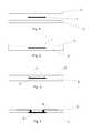
- FIG. 1shows the general arrangement of the substrate layers and the integrated circuit
- FIG. 2shows the substrate layers and the integrated circuit after lamination
- FIG. 3shows the integrated circuit laminated between the layers of the substrate whereby the holes for connecting the integrated circuit with the conductive structure have already been drilled;
- FIG. 4shows the integrated circuit laminated into the substrate with the conductive structure on top of the substrate being contacted with the chip.
- an integrated circuit (IC) 1is arranged between a first substrate layer 2 and a second substrate layer 3 .
- the IC 1can be attached either by using glue or directly to the substrate material by using thermal or ultrasonic processes. This arrangement is then laminated to give the structure as shown in FIG. 2 . Due to the low IC 1 thickness the substrate layers 2 , 3 are nearly parallel and the IC 1 is hermetically sealed and well protected by the substrate layers 2 , 3 .
- holes 4are made in the substrate layer 3 above the contacting surfaces of the IC 1 to give a structure as shown in FIG. 3 .
- the contacting surfaces of the IC 1such as, e.g., bond pads or bumps, are now in open connection to the ambience.
- the conductive structure 5is printed on the surface of the second surface layer 3 with a conductive ink, so that the formation of the conductive structure, e.g. the antenna, and its coupling to the IC 1 via conductive material in the holes 4 are effected in one single process step.
- the conductive structure 5is formed by structuring and etching the substrate 3 and the connection to the IC 1 is achieved by applying a conductive paste or a conductive adhesive in the holes 4 .
- forming the conductive structure 5 on the surface of the second surface layer 3can also be done before drilling the holes or even before lamination.
Landscapes
- Engineering & Computer Science (AREA)
- Computer Hardware Design (AREA)
- Microelectronics & Electronic Packaging (AREA)
- Physics & Mathematics (AREA)
- General Physics & Mathematics (AREA)
- Power Engineering (AREA)
- Condensed Matter Physics & Semiconductors (AREA)
- Theoretical Computer Science (AREA)
- Manufacturing & Machinery (AREA)
- Credit Cards Or The Like (AREA)
- Production Of Multi-Layered Print Wiring Board (AREA)
Abstract
Description
- arranging an integrated circuit between two layers of a substrate, said circuit having at least one contacting surface,
- forming a hole in at least one substrate layer above said at least one contacting surface and
- forming a conductive structure on a surface of said at least one substrate layer facing away from the integrated circuit and connecting said conductive structure to said contacting surface by means of said hole, said steps of forming a conductive structure and of connecting said conductive structure being advantageously performed in a single process step.
Claims (15)
Applications Claiming Priority (4)
| Application Number | Priority Date | Filing Date | Title |
|---|---|---|---|
| EP08104215.2 | 2008-06-02 | ||
| EP08104215 | 2008-06-02 | ||
| EP08104215 | 2008-06-02 | ||
| PCT/IB2009/051964WO2009147546A1 (en) | 2008-06-02 | 2009-05-13 | Method for manufacturing an electronic device |
Publications (2)
| Publication Number | Publication Date |
|---|---|
| US20110189824A1 US20110189824A1 (en) | 2011-08-04 |
| US8695207B2true US8695207B2 (en) | 2014-04-15 |
Family
ID=40957767
Family Applications (1)
| Application Number | Title | Priority Date | Filing Date |
|---|---|---|---|
| US12/995,797ActiveUS8695207B2 (en) | 2008-06-02 | 2009-05-13 | Method for manufacturing an electronic device |
Country Status (4)
| Country | Link |
|---|---|
| US (1) | US8695207B2 (en) |
| EP (1) | EP2286445A1 (en) |
| CN (1) | CN102047402B (en) |
| WO (1) | WO2009147546A1 (en) |
Cited By (1)
| Publication number | Priority date | Publication date | Assignee | Title |
|---|---|---|---|---|
| US20130318778A1 (en)* | 2012-06-01 | 2013-12-05 | Tzuh-Suan Wang | Method for manufacturing antenna structure |
Families Citing this family (6)
| Publication number | Priority date | Publication date | Assignee | Title |
|---|---|---|---|---|
| KR20130016682A (en)* | 2011-08-08 | 2013-02-18 | 에스케이하이닉스 주식회사 | Semiconductor chip having the structure of dual layer, packages having the same, and method of fabricating the semiconductor chip and package |
| DE102011114635A1 (en)* | 2011-10-04 | 2013-04-04 | Smartrac Ip B.V. | Chip card and method for producing a chip card |
| US9167684B2 (en) | 2013-05-24 | 2015-10-20 | Nokia Technologies Oy | Apparatus and method for forming printed circuit board using fluid reservoirs and connected fluid channels |
| CN106624387B (en)* | 2016-12-07 | 2018-08-10 | 诺得卡(上海)微电子有限公司 | A kind of hole punched device for smart card module manufacture |
| EP3797439A4 (en)* | 2018-05-21 | 2022-03-02 | 3M Innovative Properties Company | Ultrathin and flexible devices including circuit dies |
| DE102023120408B4 (en)* | 2023-08-01 | 2025-02-20 | Infineon Technologies Ag | Method for producing a chip card inlay, chip card inlay and chip card |
Citations (24)
| Publication number | Priority date | Publication date | Assignee | Title |
|---|---|---|---|---|
| DE19518936A1 (en) | 1995-05-23 | 1995-12-21 | Christian Dr Ing Philipp | Mounting of component to thermoplastic container wall |
| CA2128947A1 (en) | 1994-07-27 | 1996-01-28 | Jean-Noel Audoux | Process for inserting a microcircuit into the body of an intelligent card and/or memory card, and card comprising a microcircuit thus inserted |
| US5545291A (en)* | 1993-12-17 | 1996-08-13 | The Regents Of The University Of California | Method for fabricating self-assembling microstructures |
| US5800763A (en) | 1994-10-06 | 1998-09-01 | Giesecke & Devrient Gmbh | Method for producing data carriers with embedded elements |
| US5810959A (en) | 1996-02-28 | 1998-09-22 | Kabushiki Kaisha Toshiba | Thermocompressing bonding method and thermocompressing bonding apparatus |
| US5913110A (en)* | 1996-02-26 | 1999-06-15 | Herbst; Richard | Method for producing a plastic material composite component, a plastic material composite component and a mold for injection molding same |
| JP2000113147A (en) | 1998-10-08 | 2000-04-21 | Hitachi Chem Co Ltd | Ic card and its manufacture |
| US6077382A (en) | 1997-05-09 | 2000-06-20 | Citizen Watch Co., Ltd | Mounting method of semiconductor chip |
| US6080668A (en)* | 1996-05-30 | 2000-06-27 | International Business Machines Corporation | Sequential build-up organic chip carrier and method of manufacture |
| EP1014302A1 (en) | 1998-07-08 | 2000-06-28 | Dai Nippon Printing Co., Ltd. | Noncontact ic card and manufacture thereof |
| US6113728A (en) | 1989-03-09 | 2000-09-05 | Hitachi Chemical Company, Ltd. | Process for connecting circuits and adhesive film used therefor |
| US6202931B1 (en) | 1996-06-07 | 2001-03-20 | Schlumberger Systemes | Memory card and method for producing same |
| WO2002049093A1 (en) | 2000-12-11 | 2002-06-20 | Rafsec Oy | A smart label web and a method for its manufacture |
| US20040145874A1 (en) | 2003-01-23 | 2004-07-29 | Stephane Pinel | Method, system, and apparatus for embedding circuits |
| US20050093172A1 (en) | 2003-10-10 | 2005-05-05 | Norihito Tsukahara | Electronic circuit device, and method and apparatus for manufacturing the same |
| WO2005104229A1 (en) | 2004-04-16 | 2005-11-03 | eupec Europäische Gesellschaft für Leistungshalbleiter mbH | Power semiconductor arrangement |
| WO2007075352A2 (en) | 2005-12-21 | 2007-07-05 | Avery Dennison Corporation | Rfid tag film embossing manufacturing techniques |
| US20070158804A1 (en) | 2006-01-10 | 2007-07-12 | Semiconductor Energy Laboratory Co., Ltd. | Semiconductor device, manufacturing method of semiconductor device, and RFID tag |
| US7253735B2 (en)* | 2003-03-24 | 2007-08-07 | Alien Technology Corporation | RFID tags and processes for producing RFID tags |
| US20080217413A1 (en)* | 2006-08-11 | 2008-09-11 | Colin Tanner | Method and apparatus for a contactless smartcard incorporating a mechanical switch |
| US20080297350A1 (en)* | 2005-12-05 | 2008-12-04 | Nec Corporation | Rfid Tag |
| US7504297B2 (en)* | 2006-04-20 | 2009-03-17 | Renesas Technology Corp. | Semiconductor device and a method of manufacturing the same |
| US20090072413A1 (en) | 2007-09-19 | 2009-03-19 | Infineon Technologies Ag | Semiconductor device |
| WO2009147547A1 (en) | 2008-06-02 | 2009-12-10 | Nxp B.V. | Electronic device and method of manufacturing an electronic device |
- 2009
- 2009-05-13EPEP09757898Apatent/EP2286445A1/enactivePending
- 2009-05-13CNCN200980120285.XApatent/CN102047402B/enactiveActive
- 2009-05-13WOPCT/IB2009/051964patent/WO2009147546A1/enactiveApplication Filing
- 2009-05-13USUS12/995,797patent/US8695207B2/enactiveActive
Patent Citations (25)
| Publication number | Priority date | Publication date | Assignee | Title |
|---|---|---|---|---|
| US6113728A (en) | 1989-03-09 | 2000-09-05 | Hitachi Chemical Company, Ltd. | Process for connecting circuits and adhesive film used therefor |
| US5545291A (en)* | 1993-12-17 | 1996-08-13 | The Regents Of The University Of California | Method for fabricating self-assembling microstructures |
| CA2128947A1 (en) | 1994-07-27 | 1996-01-28 | Jean-Noel Audoux | Process for inserting a microcircuit into the body of an intelligent card and/or memory card, and card comprising a microcircuit thus inserted |
| US5800763A (en) | 1994-10-06 | 1998-09-01 | Giesecke & Devrient Gmbh | Method for producing data carriers with embedded elements |
| DE19518936A1 (en) | 1995-05-23 | 1995-12-21 | Christian Dr Ing Philipp | Mounting of component to thermoplastic container wall |
| US5913110A (en)* | 1996-02-26 | 1999-06-15 | Herbst; Richard | Method for producing a plastic material composite component, a plastic material composite component and a mold for injection molding same |
| US5810959A (en) | 1996-02-28 | 1998-09-22 | Kabushiki Kaisha Toshiba | Thermocompressing bonding method and thermocompressing bonding apparatus |
| US6080668A (en)* | 1996-05-30 | 2000-06-27 | International Business Machines Corporation | Sequential build-up organic chip carrier and method of manufacture |
| US6202931B1 (en) | 1996-06-07 | 2001-03-20 | Schlumberger Systemes | Memory card and method for producing same |
| US6077382A (en) | 1997-05-09 | 2000-06-20 | Citizen Watch Co., Ltd | Mounting method of semiconductor chip |
| EP1014302A1 (en) | 1998-07-08 | 2000-06-28 | Dai Nippon Printing Co., Ltd. | Noncontact ic card and manufacture thereof |
| JP2000113147A (en) | 1998-10-08 | 2000-04-21 | Hitachi Chem Co Ltd | Ic card and its manufacture |
| WO2002049093A1 (en) | 2000-12-11 | 2002-06-20 | Rafsec Oy | A smart label web and a method for its manufacture |
| US20040145874A1 (en) | 2003-01-23 | 2004-07-29 | Stephane Pinel | Method, system, and apparatus for embedding circuits |
| US7253735B2 (en)* | 2003-03-24 | 2007-08-07 | Alien Technology Corporation | RFID tags and processes for producing RFID tags |
| US20050093172A1 (en) | 2003-10-10 | 2005-05-05 | Norihito Tsukahara | Electronic circuit device, and method and apparatus for manufacturing the same |
| WO2005104229A1 (en) | 2004-04-16 | 2005-11-03 | eupec Europäische Gesellschaft für Leistungshalbleiter mbH | Power semiconductor arrangement |
| US20070200227A1 (en)* | 2004-04-16 | 2007-08-30 | Thomas Licht | Power semiconductor arrangement |
| US20080297350A1 (en)* | 2005-12-05 | 2008-12-04 | Nec Corporation | Rfid Tag |
| WO2007075352A2 (en) | 2005-12-21 | 2007-07-05 | Avery Dennison Corporation | Rfid tag film embossing manufacturing techniques |
| US20070158804A1 (en) | 2006-01-10 | 2007-07-12 | Semiconductor Energy Laboratory Co., Ltd. | Semiconductor device, manufacturing method of semiconductor device, and RFID tag |
| US7504297B2 (en)* | 2006-04-20 | 2009-03-17 | Renesas Technology Corp. | Semiconductor device and a method of manufacturing the same |
| US20080217413A1 (en)* | 2006-08-11 | 2008-09-11 | Colin Tanner | Method and apparatus for a contactless smartcard incorporating a mechanical switch |
| US20090072413A1 (en) | 2007-09-19 | 2009-03-19 | Infineon Technologies Ag | Semiconductor device |
| WO2009147547A1 (en) | 2008-06-02 | 2009-12-10 | Nxp B.V. | Electronic device and method of manufacturing an electronic device |
Non-Patent Citations (2)
| Title |
|---|
| "Etch.", Merriam-Webster.com. 2013. https://www.merriam-webster.com (Apr. 5, 2013).* |
| "Substrate" OED.com. 2012. http://oed.com/view/Entry/193100?rskey=WKs4NJ&result=l&isAdvanced=false#eid (Aug. 15, 2012).* |
Cited By (2)
| Publication number | Priority date | Publication date | Assignee | Title |
|---|---|---|---|---|
| US20130318778A1 (en)* | 2012-06-01 | 2013-12-05 | Tzuh-Suan Wang | Method for manufacturing antenna structure |
| US9112265B2 (en)* | 2012-06-01 | 2015-08-18 | Wistron Neweb Corporation | Method for manufacturing antenna structure |
Also Published As
| Publication number | Publication date |
|---|---|
| WO2009147546A1 (en) | 2009-12-10 |
| EP2286445A1 (en) | 2011-02-23 |
| CN102047402A (en) | 2011-05-04 |
| CN102047402B (en) | 2017-11-03 |
| US20110189824A1 (en) | 2011-08-04 |
Similar Documents
| Publication | Publication Date | Title |
|---|---|---|
| US9773201B2 (en) | Electronic interface apparatus and method and system for manufacturing same | |
| US8695207B2 (en) | Method for manufacturing an electronic device | |
| KR102069334B1 (en) | Method for producing a circuit for a chip card module and circuit for a chip card module | |
| US11222861B2 (en) | Dual-interface IC card module | |
| US7777317B2 (en) | Card and manufacturing method | |
| US10366320B2 (en) | Dual-interface IC card | |
| JP2004310619A (en) | Method for manufacturing ic card | |
| US20110073357A1 (en) | Electronic device and method of manufacturing an electronic device | |
| CN105512715A (en) | Chip card module arrangement, chip card arrangement and method for producing a chip card arrangement | |
| JP4579924B2 (en) | Production method of card having dual interface and microcircuit card obtained by the same method | |
| CN109583552B (en) | Method for manufacturing portable data carrier and data carrier body | |
| US10395158B2 (en) | Method for making an anti-crack electronic device | |
| CN100468450C (en) | Method for mounting electronic devices on substrates | |
| US20220068789A1 (en) | Package, method for forming a package, carrier tape, chip card and method for forming a carrier tape | |
| JP4952266B2 (en) | Dual interface IC card and its manufacturing method, contact / non-contact IC module | |
| KR100769204B1 (en) | Semiconductor package and manufacturing method | |
| WO2021255490A1 (en) | A method of forming a smart card, a prelam body, and a smart card | |
| MX2008012339A (en) | Methods for attaching a flip chip integrated circuit assembly to a substrate. | |
| JP2008235838A (en) | Semiconductor device, manufacturing method thereof, mounting method thereof, and IC card using the same | |
| JP5024190B2 (en) | IC module manufacturing method | |
| JP2000269254A (en) | Semiconductor package and manufacturing method thereof |
Legal Events
| Date | Code | Title | Description |
|---|---|---|---|
| AS | Assignment | Owner name:NXP B.V., NETHERLANDS Free format text:ASSIGNMENT OF ASSIGNORS INTEREST;ASSIGNOR:ZENZ, CHRISTIAN;REEL/FRAME:026143/0203 Effective date:20110404 | |
| STCF | Information on status: patent grant | Free format text:PATENTED CASE | |
| AS | Assignment | Owner name:MORGAN STANLEY SENIOR FUNDING, INC., MARYLAND Free format text:SECURITY AGREEMENT SUPPLEMENT;ASSIGNOR:NXP B.V.;REEL/FRAME:038017/0058 Effective date:20160218 | |
| AS | Assignment | Owner name:MORGAN STANLEY SENIOR FUNDING, INC., MARYLAND Free format text:CORRECTIVE ASSIGNMENT TO CORRECT THE REMOVE APPLICATION 12092129 PREVIOUSLY RECORDED ON REEL 038017 FRAME 0058. ASSIGNOR(S) HEREBY CONFIRMS THE SECURITY AGREEMENT SUPPLEMENT;ASSIGNOR:NXP B.V.;REEL/FRAME:039361/0212 Effective date:20160218 | |
| AS | Assignment | Owner name:MORGAN STANLEY SENIOR FUNDING, INC., MARYLAND Free format text:CORRECTIVE ASSIGNMENT TO CORRECT THE REMOVE APPLICATION 12681366 PREVIOUSLY RECORDED ON REEL 038017 FRAME 0058. ASSIGNOR(S) HEREBY CONFIRMS THE SECURITY AGREEMENT SUPPLEMENT;ASSIGNOR:NXP B.V.;REEL/FRAME:042985/0001 Effective date:20160218 Owner name:MORGAN STANLEY SENIOR FUNDING, INC., MARYLAND Free format text:CORRECTIVE ASSIGNMENT TO CORRECT THE REMOVE APPLICATION 12681366 PREVIOUSLY RECORDED ON REEL 039361 FRAME 0212. ASSIGNOR(S) HEREBY CONFIRMS THE SECURITY AGREEMENT SUPPLEMENT;ASSIGNOR:NXP B.V.;REEL/FRAME:042762/0145 Effective date:20160218 | |
| MAFP | Maintenance fee payment | Free format text:PAYMENT OF MAINTENANCE FEE, 4TH YEAR, LARGE ENTITY (ORIGINAL EVENT CODE: M1551) Year of fee payment:4 | |
| AS | Assignment | Owner name:NXP B.V., NETHERLANDS Free format text:RELEASE BY SECURED PARTY;ASSIGNOR:MORGAN STANLEY SENIOR FUNDING, INC.;REEL/FRAME:050745/0001 Effective date:20190903 | |
| AS | Assignment | Owner name:MORGAN STANLEY SENIOR FUNDING, INC., MARYLAND Free format text:CORRECTIVE ASSIGNMENT TO CORRECT THE REMOVE APPLICATION 12298143 PREVIOUSLY RECORDED ON REEL 042762 FRAME 0145. ASSIGNOR(S) HEREBY CONFIRMS THE SECURITY AGREEMENT SUPPLEMENT;ASSIGNOR:NXP B.V.;REEL/FRAME:051145/0184 Effective date:20160218 Owner name:MORGAN STANLEY SENIOR FUNDING, INC., MARYLAND Free format text:CORRECTIVE ASSIGNMENT TO CORRECT THE REMOVE APPLICATION 12298143 PREVIOUSLY RECORDED ON REEL 039361 FRAME 0212. ASSIGNOR(S) HEREBY CONFIRMS THE SECURITY AGREEMENT SUPPLEMENT;ASSIGNOR:NXP B.V.;REEL/FRAME:051029/0387 Effective date:20160218 Owner name:MORGAN STANLEY SENIOR FUNDING, INC., MARYLAND Free format text:CORRECTIVE ASSIGNMENT TO CORRECT THE REMOVE APPLICATION 12298143 PREVIOUSLY RECORDED ON REEL 042985 FRAME 0001. ASSIGNOR(S) HEREBY CONFIRMS THE SECURITY AGREEMENT SUPPLEMENT;ASSIGNOR:NXP B.V.;REEL/FRAME:051029/0001 Effective date:20160218 Owner name:MORGAN STANLEY SENIOR FUNDING, INC., MARYLAND Free format text:CORRECTIVE ASSIGNMENT TO CORRECT THE REMOVE APPLICATION12298143 PREVIOUSLY RECORDED ON REEL 042762 FRAME 0145. ASSIGNOR(S) HEREBY CONFIRMS THE SECURITY AGREEMENT SUPPLEMENT;ASSIGNOR:NXP B.V.;REEL/FRAME:051145/0184 Effective date:20160218 Owner name:MORGAN STANLEY SENIOR FUNDING, INC., MARYLAND Free format text:CORRECTIVE ASSIGNMENT TO CORRECT THE REMOVE APPLICATION 12298143 PREVIOUSLY RECORDED ON REEL 038017 FRAME 0058. ASSIGNOR(S) HEREBY CONFIRMS THE SECURITY AGREEMENT SUPPLEMENT;ASSIGNOR:NXP B.V.;REEL/FRAME:051030/0001 Effective date:20160218 Owner name:MORGAN STANLEY SENIOR FUNDING, INC., MARYLAND Free format text:CORRECTIVE ASSIGNMENT TO CORRECT THE REMOVE APPLICATION12298143 PREVIOUSLY RECORDED ON REEL 039361 FRAME 0212. ASSIGNOR(S) HEREBY CONFIRMS THE SECURITY AGREEMENT SUPPLEMENT;ASSIGNOR:NXP B.V.;REEL/FRAME:051029/0387 Effective date:20160218 Owner name:MORGAN STANLEY SENIOR FUNDING, INC., MARYLAND Free format text:CORRECTIVE ASSIGNMENT TO CORRECT THE REMOVE APPLICATION12298143 PREVIOUSLY RECORDED ON REEL 042985 FRAME 0001. ASSIGNOR(S) HEREBY CONFIRMS THE SECURITY AGREEMENT SUPPLEMENT;ASSIGNOR:NXP B.V.;REEL/FRAME:051029/0001 Effective date:20160218 | |
| MAFP | Maintenance fee payment | Free format text:PAYMENT OF MAINTENANCE FEE, 8TH YEAR, LARGE ENTITY (ORIGINAL EVENT CODE: M1552); ENTITY STATUS OF PATENT OWNER: LARGE ENTITY Year of fee payment:8 |