US8694854B1 - Read threshold setting based on soft readout statistics - Google Patents
Read threshold setting based on soft readout statisticsDownload PDFInfo
- Publication number
- US8694854B1 US8694854B1US13/195,852US201113195852AUS8694854B1US 8694854 B1US8694854 B1US 8694854B1US 201113195852 AUS201113195852 AUS 201113195852AUS 8694854 B1US8694854 B1US 8694854B1
- Authority
- US
- United States
- Prior art keywords
- read
- memory cells
- output values
- data
- thresholds
- Prior art date
- Legal status (The legal status is an assumption and is not a legal conclusion. Google has not performed a legal analysis and makes no representation as to the accuracy of the status listed.)
- Active, expires
Links
- 238000000034methodMethods0.000claimsabstractdescription86
- 238000013500data storageMethods0.000claimsabstractdescription22
- 238000009826distributionMethods0.000claimsdescription48
- 238000000926separation methodMethods0.000claimsdescription26
- 238000013507mappingMethods0.000claimsdescription23
- 238000012937correctionMethods0.000claimsdescription14
- 230000001186cumulative effectEffects0.000claimsdescription4
- 238000005315distribution functionMethods0.000claimsdescription4
- 230000001419dependent effectEffects0.000claims1
- 230000008569processEffects0.000description18
- 238000004891communicationMethods0.000description14
- 238000012360testing methodMethods0.000description5
- 230000006870functionEffects0.000description4
- 206010011906DeathDiseases0.000description2
- 230000006978adaptationEffects0.000description2
- 238000003491arrayMethods0.000description2
- 230000008859changeEffects0.000description2
- 230000001351cycling effectEffects0.000description2
- 230000006735deficitEffects0.000description2
- 238000010586diagramMethods0.000description2
- 230000008901benefitEffects0.000description1
- 230000001413cellular effectEffects0.000description1
- 238000006243chemical reactionMethods0.000description1
- 230000007423decreaseEffects0.000description1
- 238000001514detection methodMethods0.000description1
- 230000000694effectsEffects0.000description1
- 230000014759maintenance of locationEffects0.000description1
- 238000012986modificationMethods0.000description1
- 230000004048modificationEffects0.000description1
- 150000004767nitridesChemical class0.000description1
- 230000003287optical effectEffects0.000description1
- 239000004065semiconductorSubstances0.000description1
- 238000012163sequencing techniqueMethods0.000description1
- 239000007787solidSubstances0.000description1
Images


Classifications
- G—PHYSICS
- G11—INFORMATION STORAGE
- G11C—STATIC STORES
- G11C29/00—Checking stores for correct operation ; Subsequent repair; Testing stores during standby or offline operation
- G11C29/52—Protection of memory contents; Detection of errors in memory contents
- G—PHYSICS
- G11—INFORMATION STORAGE
- G11C—STATIC STORES
- G11C11/00—Digital stores characterised by the use of particular electric or magnetic storage elements; Storage elements therefor
- G11C11/56—Digital stores characterised by the use of particular electric or magnetic storage elements; Storage elements therefor using storage elements with more than two stable states represented by steps, e.g. of voltage, current, phase, frequency
- G11C11/5621—Digital stores characterised by the use of particular electric or magnetic storage elements; Storage elements therefor using storage elements with more than two stable states represented by steps, e.g. of voltage, current, phase, frequency using charge storage in a floating gate
- G11C11/5642—Sensing or reading circuits; Data output circuits
- G—PHYSICS
- G11—INFORMATION STORAGE
- G11C—STATIC STORES
- G11C11/00—Digital stores characterised by the use of particular electric or magnetic storage elements; Storage elements therefor
- G11C11/56—Digital stores characterised by the use of particular electric or magnetic storage elements; Storage elements therefor using storage elements with more than two stable states represented by steps, e.g. of voltage, current, phase, frequency
- G11C11/5685—Digital stores characterised by the use of particular electric or magnetic storage elements; Storage elements therefor using storage elements with more than two stable states represented by steps, e.g. of voltage, current, phase, frequency using storage elements comprising metal oxide memory material, e.g. perovskites
- G—PHYSICS
- G11—INFORMATION STORAGE
- G11C—STATIC STORES
- G11C29/00—Checking stores for correct operation ; Subsequent repair; Testing stores during standby or offline operation
- G11C29/02—Detection or location of defective auxiliary circuits, e.g. defective refresh counters
- G11C29/021—Detection or location of defective auxiliary circuits, e.g. defective refresh counters in voltage or current generators
- G—PHYSICS
- G11—INFORMATION STORAGE
- G11C—STATIC STORES
- G11C29/00—Checking stores for correct operation ; Subsequent repair; Testing stores during standby or offline operation
- G11C29/02—Detection or location of defective auxiliary circuits, e.g. defective refresh counters
- G11C29/028—Detection or location of defective auxiliary circuits, e.g. defective refresh counters with adaption or trimming of parameters
Definitions
- the present inventionrelates generally to memory devices, and particularly to methods and systems for setting read thresholds in non-volatile memory devices.
- Analog memory cellssuch as Flash memory cells
- Flash memory cellsare typically read by comparing the analog cell values to one or more read thresholds.
- Various techniques for setting and adjusting read thresholdsare known in the art. For example, U.S. Pat. No. 5,657,332, whose disclosure is incorporated herein by reference, describes methods for recovering from hard errors in a solid-state memory system.
- a memory systemincludes an array of memory cells, each cell capable of having its threshold voltage programmed or erased to an intended level.
- An error checking schemeis provided for each of a plurality of groups of cells for identifying read errors therein.
- a read reference levelis adjusted before each read operation on the individual group of cells containing read errors, each time the read reference level being displaced a predetermined step from a reference level for normal read, until the error checking means no longer indicates read errors.
- the drifted threshold voltage of each cell associated with a read erroris re-written to its intended level.
- a set of operating reference cellsis established to be used in operating cells in a Non-Volatile Memory (NVM) block or array. At least a subset of cells of the NVM block or array may be read using each of two or more sets of test reference cells, where each set of test reference cells may generate or otherwise provide reference voltages at least slightly offset from each other set of test reference cells. For each set of test reference cells used to read at least a subset of the NVM block, a read error rate may be calculated or otherwise determined. A set of test reference cells associated with a relatively low read error rate may be selected as the set of operating reference cells to be used in operating other cells, outside the subset of cells, in the NVM block or array.
- U.S. Patent Application Publication 2010/0091535whose disclosure is incorporated herein by reference, describes various techniques for adjusting read thresholds of analog memory cells.
- datais encoded with an Error Correction Code (ECC) before it is stored in the memory cells.
- ECCError Correction Code
- the ECCis decoded in order to correct read errors.
- the direction of the errori.e., the programming level with which the read storage value was erroneously associated before applying ECC correction, is determined.
- Information regarding directions of corrected errorsis used for adjusting the read thresholds.
- a method for data storageincludes storing data in analog memory cells by programming the memory cells with respective analog input values. After storing the data, respective analog output values are read from the memory cells using multiple read thresholds, which define multiple ranges of the analog output values. Respective numbers of read errors in the data, corresponding to the analog output values falling in the ranges, are assessed. The stored data is recovered based on respective numbers of the read errors assessed in the ranges.
- recovering the stored dataincludes adjusting at least one of the read thresholds based on the respective numbers of the read errors, and retrieving the data from the memory cells using the adjusted read thresholds.
- adjusting the read thresholdsincludes adapting the read thresholds based on the numbers of the read errors assessed in a first group of the memory cells, and retrieving the data includes reading the data from a second group of the memory cells using the adapted read thresholds.
- adjusting the read thresholdsincludes adapting the read thresholds based on the numbers of the read errors assessed in given group of the memory cells, and retrieving the data includes reading the data from the given group of the memory cells using the adapted read thresholds.
- adjusting the read thresholdsincludes moving the multiple read thresholds while preserving separations between the read thresholds.
- adjusting the read thresholdsincludes modifying one or more separations between the read thresholds.
- the methodincludes holding a mapping that defines multiple sets of the read thresholds depending on one or more parameters related to the analog output values, and adjusting the read thresholds includes estimating the parameters based on the read analog output values, and obtaining the read thresholds from the mapping using the estimated parameters.
- adjusting the read thresholdsincludes modeling readout of the data using a communication channel model, and adapting the read thresholds so as to maximize a capacity of the communication channel model.
- the read thresholdsinclude at least a hard threshold and two soft thresholds on opposite sides of the hard threshold, and the ranges include at least a first range between the hard threshold and one of the soft thresholds, and a second range between the hard threshold and the other of the soft thresholds.
- storing the dataincludes programming each memory cell to a respective one of multiple programming levels, and reading the analog output values includes positioning the multiple read thresholds in a boundary region between a given pair of the programming levels.
- recovering the stored dataincludes computing soft decoding metrics based on the respective numbers of the read errors, and decoding an Error Correction Code (ECC) that encodes the stored data using the soft decoding metrics.
- ECCError Correction Code
- Recovering the stored datamay include computing the soft decoding metrics over a first group of the memory cells, and decoding the ECC that encodes the data stored in a second group of the memory cells.
- storing the dataincludes encoding the data with an Error Correction Code (ECC), and assessing the numbers of the read errors includes correcting the read errors using the ECC and determining a respective count of the read errors in each range that were corrected by the ECC.
- ECCError Correction Code
- storing the dataincludes programming each memory cell to a respective one of multiple programming levels, and the analog output values corresponding to at least one of the programming levels are distributed in accordance with a non-Gaussian distribution.
- a data storage apparatusincluding an interface and circuitry.
- the interfaceis configured to communicate with a memory including analog memory cells.
- the circuitryis configured to store data in the analog memory cells of the memory by programming the memory cells with respective analog input values, to read, after storing the data, respective analog output values from the memory cells using multiple read thresholds that define multiple ranges of the analog output values, to assess a respective number of read errors in the data corresponding to the analog output values falling in each of the ranges, and to adjust at least one of the read thresholds based on respective numbers of the read errors assessed in the ranges.
- a data storage apparatusincluding a memory and circuitry.
- the memoryincludes analog memory cells.
- the circuitryis configured to store data in the analog memory cells of the memory by programming the memory cells with respective analog input values, to read, after storing the data, respective analog output values from the memory cells using multiple read thresholds that define multiple ranges of the analog output values, to assess a respective number of read errors in the data corresponding to the analog output values falling in each of the ranges, and to adjust at least one of the read thresholds based on respective numbers of the read errors assessed in the ranges.
- a method for data storageincludes storing data in analog memory cells by programming the memory cells with respective analog input values. Multiple read thresholds are set for reading respective analog output values from the memory cells. the read thresholds define multiple ranges of the analog output values and are set such that a respective number of the analog output values occurring in each range matches a respective value. The stored data is retrieved by reading the analog output values from the memory cells using the multiple read thresholds.
- setting the read thresholdsincludes estimating one or more Cumulative Distribution Functions (CDFs) of the analog output values, and setting the read thresholds based on the estimated CDFs.
- the methodincludes holding a mapping that defines multiple sets of the read thresholds depending on one or more parameters related to the analog output values, and setting the read thresholds includes estimating the parameters based on the read analog output values, and obtaining the read thresholds from the mapping using the estimated parameters.
- setting the read thresholdsincludes modeling readout of the data using a communication channel model, and adapting the read thresholds so as to maximize a capacity of the communication channel model.
- a data storage apparatusincluding an interface and circuitry.
- the interfaceis configured to communicate with a memory including analog memory cells.
- the circuitryis configured to store data in the analog memory cells by programming the memory cells with respective analog input values, to set multiple read thresholds for reading respective analog output values from the memory cells, wherein the read thresholds define multiple ranges of the analog output values and are set such that a respective number of the analog output values occurring in each range matches a respective value, and to retrieve the stored data by reading the analog output values from the memory cells using the multiple read thresholds.
- a data storage apparatusincluding a memory and circuitry.
- the memoryincludes analog memory cells.
- the circuitryis configured to store data in the analog memory cells by programming the memory cells with respective analog input values, to set multiple read thresholds for reading respective analog output values from the memory cells, wherein the read thresholds define multiple ranges of the analog output values and are set such that a respective number of the analog output values occurring in each range matches a respective value, and to retrieve the stored data by reading the analog output values from the memory cells using the multiple read thresholds.
- a method for data storageincluding holding a mapping that defines multiple sets of read thresholds for reading analog memory cells depending on one or more parameters related to analog values read from the memory cells.
- Datais stored in a group of the analog memory cells by programming the memory cells in the group with respective analog input values. After storing the data, respective analog output values are read from the memory cells in the group and the parameters are estimated based on the read analog output values.
- the read thresholdsare set for subsequent readout operations based on the mapping using the estimated parameters.
- the parametersinclude a variance of a distribution of at least some of the analog output values, a width of the distribution and/or a distance between distributions of subsets of the analog output values.
- a data storage apparatusincluding an interface and circuitry.
- the interfaceis configured to communicate with a memory including analog memory cells.
- the circuitryis configured to hold a mapping that defines multiple sets of read thresholds for reading analog memory cells depending on one or more parameters related to analog values read from the memory cells, to store data in a group of the analog memory cells by programming the memory cells in the group with respective analog input values, to read, after storing the data, respective analog output values from the memory cells in the group and to estimate the parameters based on the read analog output values, and to set the read thresholds for subsequent readout operations based on the mapping using the estimated parameters.
- a data storage apparatusincluding a memory and circuitry.
- the memoryincludes analog memory cells.
- the circuitryis configured to hold a mapping that defines multiple sets of read thresholds for reading analog memory cells depending on one or more parameters related to analog values read from the memory cells, to store data in a group of the analog memory cells by programming the memory cells in the group with respective analog input values, to read, after storing the data, respective analog output values from the memory cells in the group and to estimate the parameters based on the read analog output values, and to set the read thresholds for subsequent readout operations based on the mapping using the estimated parameters.
- a method for data storageincluding storing data in analog memory cells by programming the memory cells with respective analog input values. After storing the data, respective analog output values are read from the memory cells using multiple read thresholds. Readout of the data is modeled using a communication channel model, and the read thresholds are adapted so as to maximize a capacity of the communication channel model.
- a data storage apparatusincluding an interface and circuitry.
- the interfaceis configured to communicate with a memory including analog memory cells.
- the circuitryis configured to store data in the analog memory cells by programming the memory cells with respective analog input values, to read, after storing the data, respective analog output values from the memory cells using multiple read thresholds, to model readout of the data using a communication channel model, and to adapt the read thresholds so as to maximize a capacity of the communication channel model.
- a data storage apparatusincluding a memory and circuitry.
- the memoryincludes analog memory cells.
- the circuitryis configured to store data in the analog memory cells by programming the memory cells with respective analog input values, to read, after storing the data, respective analog output values from the memory cells using multiple read thresholds, to model readout of the data using a communication channel model, and to adapt the read thresholds so as to maximize a capacity of the communication channel model.
- FIG. 1is a block diagram that schematically illustrates a memory system, in accordance with an embodiment of the present invention
- FIG. 2is a graph showing threshold voltage distributions and read thresholds in a group of analog memory cells, in accordance with an embodiment of the present invention.
- FIG. 3is a flow chart that schematically illustrates a method for adjusting read thresholds, in accordance with an embodiment of the present invention.
- datais stored in analog memory cells by programming the memory cells to respective analog input values that represent the stored bit values.
- Datais retrieved by comparing respective analog output values of the memory cells to one or more read thresholds.
- each bit valuecorresponds to a respective programming level that is represented by a certain region of analog output values.
- the relation between the analog output value of a given memory cell and the read thresholdsis indicative of the memory cell's programming level, and thus of the data stored in that memory cell.
- Analog output valuesmay drift over time and may be subject to various types of impairments. Thus, proper setting and adaptation of the read thresholds is important for maintaining low read error probability.
- Embodiments of the present inventionthat are described herein provide improved methods and systems for setting read thresholds used for reading analog memory cells.
- the disclosed techniquesare based on reading the memory cells using multiple read thresholds.
- the multiple read thresholdsare typically all positioned in a boundary region between a given pair of programming levels. Positioning of the read thresholds defines multiple ranges of output values between the thresholds.
- each rangethe number of read errors in the data corresponding to the analog output values falling in the range is assessed.
- the number of memory cells whose output value falls in the range even though their stored data corresponds to a different rangeis assessed separately for each range.
- One or more of the read thresholdsare adjusted based on the numbers of read errors assessed for the different output value ranges.
- the stored datais encoded with an Error Correction Code (ECC), and the numbers of errors for the different ranges are obtained from the ECC decoding process.
- ECCError Correction Code
- the disclosed techniquesare able to focus on subsets of the read errors that are meaningful for threshold setting. As such, the disclosed techniques perform well under a wide variety of real-life output value distributions, such as various non-Gaussian distributions.
- One example of such a distributionis caused by “stuck bits,” i.e., memory cells whose output values remain fixed and do not respond to programming.
- Some embodimentsuse hard ECC decoding and others use soft decoding.
- the assessed numbers of errors for the different output value rangesare used to improve initial soft decoding metrics (e.g., Log Likelihood Ratios LLRs) used for soft ECC decoding.
- initial soft decoding metricse.g., Log Likelihood Ratios LLRs
- multiple sets of read thresholdsare stored in a Look-Up Table (LUT), and the appropriate set is chosen based on the read output values.
- Other disclosed techniquesadjust the read thresholds such that the absolute number of output values falling in each range of output values matches a respective target number.
- the data readout processis modeled in terms of a communication channel, and the read thresholds are adapted so as to maximize the channel capacity.
- FIG. 1is a block diagram that schematically illustrates a memory system 20 , in accordance with an embodiment of the present invention.
- System 20can be used in various host systems and devices, such as in computing devices, cellular phones or other communication terminals, removable memory modules (sometimes referred to as “Flash drives”), Solid State Disks (SSD), digital cameras, music and other media players and/or any other system or device in which data is stored and retrieved.
- flash drivessometimes referred to as “Flash drives”
- SSDSolid State Disks
- Digital camerasmusic and other media players and/or any other system or device in which data is stored and retrieved.
- System 20comprises a memory device 24 , which stores data in a memory cell array 28 .
- the memory arraycomprises multiple analog memory cells 32 that are arranged in word lines 34 .
- analog memory cellis used to describe any memory cell that holds a continuous, analog value of a physical parameter, such as an electrical voltage or charge.
- Array 32may comprise solid-state analog memory cells of any kind, such as, for example, NAND, NOR and Charge Trap Flash (CTF) Flash cells, phase change RAM (PRAM, also referred to as Phase Change Memory—PCM), Nitride Read Only Memory (NROM), Ferroelectric RAM (FRAM), magnetic RAM (MRAM) and/or Dynamic RAM (DRAM) cells.
- PCMphase change RAM
- NROMNitride Read Only Memory
- FRAMFerroelectric RAM
- MRAMmagnetic RAM
- DRAMDynamic RAM
- analog valuesstorage values or analog storage values.
- analog values written to the memory cellsare referred to herein as input analog values, and the analog values read from the memory cells are referred to as analog output values.
- System 20stores data in the analog memory cells by programming the cells to assume respective memory states, which are also referred to as programming states or programming levels.
- the programming levelsare selected from a finite set of possible levels, and each level corresponds to a certain nominal storage value.
- a 2 bit/cell MLCcan be programmed to assume one of four possible programming levels by writing one of four possible nominal storage values into the cell.
- the techniques described hereinmainly address storage densities of a non-integer number of bits per memory cell, i.e., a number of programming levels per cell that is not an integer power of two.
- Memory device 24comprises a reading/writing (R/W) unit 36 , which converts data for storage in the memory device to analog storage values and writes them into memory cells 32 .
- the R/W unitdoes not perform the conversion, but is provided with voltage samples, i.e., with the storage values for storage in the cells.
- R/W unit 36converts the storage values of memory cells into digital samples having a resolution of one or more bits. Data is typically written to and read from the memory cells in groups that are referred to as pages.
- the R/W unitcan erase a group of cells 32 by applying one or more negative erasure pulses to the cells.
- Memory controller 40comprises an interface 44 for communicating with memory device 24 , and a processor 48 .
- the disclosed techniquescan be carried out by memory controller 40 , by R/W unit 36 , or both.
- memory controller 40 and R/W unit 36are referred to collectively as circuitry that carries out the disclosed techniques.
- Memory controller 40communicates with a host 52 , for accepting data for storage in the memory device and for outputting data retrieved from the memory device.
- Memory controller 40may be implemented in hardware, e.g., using one or more Application-Specific Integrated Circuits (ASICs) or Field-Programmable Gate Arrays (FPGAs).
- ASICsApplication-Specific Integrated Circuits
- FPGAsField-Programmable Gate Arrays
- the memory controllermay comprise a microprocessor that runs suitable software, or a combination of hardware and software elements.
- FIG. 1is an example system configuration, which is shown purely for the sake of conceptual clarity. Any other suitable memory system configuration can also be used.
- memory controller 40may control multiple memory devices 24 . Elements that are not necessary for understanding the principles of the present invention, such as various interfaces, addressing circuits, timing and sequencing circuits and debugging circuits, have been omitted from the figure for clarity.
- memory device 24 and memory controller 40are implemented as two separate Integrated Circuits (ICs).
- the memory device and the memory controllermay be integrated on separate semiconductor dies in a single Multi-Chip Package (MCP) or System on Chip (SoC), and may be interconnected by an internal bus.
- MCPMulti-Chip Package
- SoCSystem on Chip
- some or all of the memory controller circuitrymay reside on the same die on which the memory array is disposed.
- some or all of the functionality of memory controller 40can be implemented in software and carried out by a processor or other element of the host system.
- host 52 and memory controller 40may be fabricated on the same die, or on separate dies in the same device package.
- memory controller 40comprises a general-purpose processor, which is programmed in software to carry out the functions described herein.
- the softwaremay be downloaded to the processor in electronic form, over a network, for example, or it may, alternatively or additionally, be provided and/or stored on non-transitory tangible media, such as magnetic, optical, or electronic memory.
- memory cells 32are arranged in multiple rows and columns, and each memory cell comprises a floating-gate transistor.
- the gates of the transistors in each roware connected by word lines 34
- the sources of the transistors in each columnare connected by bit lines.
- the term “row”is used in the conventional sense to mean a group of memory cells that are fed by a common word line
- the term “column”means a group of memory cells fed by a common bit line.
- the terms “row” and “column”do not connote a certain physical orientation of the memory cells relative to the memory device.
- the memory arrayis typically divided into multiple memory pages, i.e., groups of memory cells that are programmed and read simultaneously.
- memory pagesare sub-divided into sectors. Pages may be mapped to word lines in various manners. Each word line may store one or more pages. A given page may be stored in all the memory cells of a word line, or in a subset of the memory cells (e.g., the odd-order or even-order memory cells).
- Erasing of cellsis usually carried out in blocks that contain multiple pages.
- Typical memory devicesmay comprise thousands of erasure blocks.
- each erasure blockis on the order of 32 word lines, each comprising several tens of thousands of cells. Each word line of such a device is often partitioned into four pages (odd/even order cells, least/most significant bit of the cells).
- Three-bit-per cell devices having 32 word lines per erasure blockwould have 192 pages per erasure block, and four-bit-per-cell devices would have 256 pages per block.
- Other block sizes and configurationscan also be used.
- Some memory devicescomprise two or more separate memory cell arrays, often referred to as planes. Since each plane has a certain “busy” period between successive write operations, data can be written alternately to the different planes in order to increase programming speed.
- memory controller 40reads a group of memory cells 32 , e.g., a word line or part of a word line, using multiple read thresholds.
- the memory controllerdecodes the stored data based on the read results, i.e., based on where each cell output value falls relative to the read thresholds.
- the memory controllersets and adjusts the positions of the read thresholds using methods that are described below.
- the description that followsrefers to a specific embodiment involving two programming levels and three read thresholds.
- the disclosed techniquesare in no way limited to this embodiment, and can be generalized in a straightforward manner to any desired number of programming levels and read thresholds.
- the description that followsrefers to the disclosed techniques as being carried out by memory controller 40 . In alternative embodiments, however, these techniques can be carried out by R/W unit 36 in the memory device, or jointly by the R/W unit and the memory controller.
- FIG. 2is a graph showing threshold voltage distributions and read thresholds in a group of analog memory cells, in accordance with an embodiment of the present invention.
- the memory cellsare programmed to two programming levels corresponding to “1” and “0” bit values, respectively.
- the threshold voltages (V TH ) of the memory cells programmed with “1”are distributed in accordance with a distribution 60 A
- the threshold voltages of the memory cells programmed with “0”are distributed in accordance with a distribution 60 B.
- the threshold voltage distributionsare not necessarily Gaussian or even symmetric, and are not necessarily similar to one another.
- the memory cellsare not necessarily divided evenly between the programming levels.
- the stored datais encoded prior to storage with an Error Correction Code (ECC), such as a Bose-Chaudhuri-Hocquenghem (BCH) code, a Low-Density Parity Check (LDPC) code or any other suitable ECC.
- ECCError Correction Code
- the memory controllerdecodes the ECC in a hard decoding process, i.e., based on a binary input for each bit.
- the memory controllerdecodes the ECC in a soft decoding process, based on soft decoding metrics (e.g., Log Likelihood Ratios—LLRs) that are computed for the bits.
- soft decoding metricse.g., Log Likelihood Ratios—LLRs
- Memory controller 40retrieves the data from the group of memory cells by setting (using R/W unit 36 ) one or more read thresholds, and comparing the threshold voltages of the memory cells to the read thresholds.
- memory controller 40sets a total of three thresholds—A hard threshold 64 and two soft thresholds 68 A and 68 B on opposite sides of the hard threshold. All three thresholds are positioned in the boundary region between the two programming levels in question.
- memory controller 40adjusts the position of hard threshold 64 using the following process:
- the memory controllerreads the memory cells using all three read thresholds (hard threshold 64 and soft thresholds 68 A and 68 B).
- the three thresholdsdefine two finite ranges (intervals) 72 A and 72 B of threshold voltages that fall between the thresholds. For each of the two ranges (intervals 72 A and 72 B), the memory controller assesses the number of read errors occurring in the range.
- a shaded region 76 Acorresponds to the memory cells that belong to distribution 60 B and whose V TH falls between thresholds 64 and 68 A.
- the area of region 76 Ais indicative of the number of read errors occurring in interval 72 A.
- a shaded region 76 Bcorresponds to the memory cells belonging to distribution 60 A and whose V TH falls between thresholds 64 and 68 B. The area of region 76 A is thus indicative of the number of read errors occurring in interval 72 B.
- memory controller 40adjusts the position of hard threshold 64 based on the number of read errors falling in intervals 72 A and 72 B. Typically, the memory controller adjusts thresholds 64 so as to equalize these two numbers. In other words, if the number of read errors in interval 72 A is greater than the number or read errors in interval 72 B, the memory controller decreases threshold 64 (i.e., moves it to the left). If the number of read errors in interval 72 A is smaller than the number or read errors in interval 72 B, the memory controller increases threshold 64 . Soft thresholds 68 A and 68 B are typically adjusted together with threshold 64 , so as to maintain the separations between the thresholds.
- the numbers of read errorsare used for deciding on the direction in which the threshold is to be adjusted, but the amount of adjustment is set regardless of these numbers (e.g., at fixed or predefined increments).
- the memory controllersets the size of the adjustment based on the numbers of read errors, e.g., based on the ratio between the numbers.
- the thresholdis adjusted based on the numbers of errors that occur in close proximity to the threshold. This choice is in contrast to basing the adjustment on the total numbers of read errors (the total number of memory cells in distribution 60 A whose V TH falls above threshold 64 , and the total number of memory cells in distribution 60 B whose V TH falls below threshold 64 ). As a result, the threshold adjustment process is not sensitive to the actual shapes of distributions 60 A and 60 B.
- the V TH distributionis approximately Gaussian, and therefore the direction and size of the read threshold adjustment can be computed with high accuracy and reliability.
- a number of memory cellsare stuck at certain threshold voltages regardless of programming. These stuck threshold voltages are, with high probability, not in the vicinity of hard threshold 64 . This phenomenon is sometimes referred to as “stuck cells” or “stuck bits.” Such stuck memory cells typically distort the shapes of the V TH distributions and cause them to deviate from Gaussian. Therefore, the correct adjustment of threshold 64 is by equalizing the total number of read errors while ignoring the “stuck cells.”
- the disclosed techniqueovercomes the distorting effect of stuck memory cells, since it considers only the read errors that occur in proximity to the hard read threshold.
- Memory controller 40may assess the numbers of read errors in the various V TH ranges (e.g., in intervals 72 A and 72 B) using any suitable method.
- the ECC decoding process in the memory controlleris able to output the number of corrected read errors (“0” to “1”, and “1” to “0”) for each interval separately.
- any other suitable methodcan be used for assessing the numbers of read errors in the various V TH ranges.
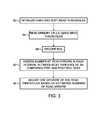
- FIG. 3is a flow chart that schematically illustrates a method for adjusting read thresholds, in accordance with an embodiment of the present invention.
- the methodbegins with memory controller 40 initializing hard threshold 64 and soft thresholds 68 A and 68 B to some initial positions, at an initialization step 80 .
- the memory controllerthen reads a group of memory cells using the three read thresholds, at a readout step 84 .
- the memory controllerdecodes the ECC, at an ECC decoding step 88 .
- ECC decodingmay be hard (i.e., based on the read results of threshold 64 ) or soft (i.e., based on the read results of thresholds 64 , 68 A and 68 B).
- Memory controller 40then assesses the number of read errors for each of intervals 72 A and 72 B between the read thresholds, at an error assessment step 92 .
- the memory controllermay compare the data before and after ECC correction, or accept from the ECC decoding process a respective count of the corrected errors for each interval.
- the memory controllerassesses the number of “0” ⁇ “1” errors in interval 72 A, and the number of “1” ⁇ “0” errors in interval 72 B.
- the memory controlleradjusts one or more of the read thresholds based on the numbers of read errors assessed for the different intervals, at a threshold adjustment step 96 .
- the memory controllerassesses the number of errors based on outputs from the ECC decoding process following successful ECC decoding. In practice, however, ECC decoding may sometimes fail. In such cases, the memory controller may attempt ECC decoding on another group of memory cells (either in the same word line or in a different word line), estimate the read threshold positions on that group, and use the resulting read threshold for reading the memory cells for which ECC decoding has failed.
- the disclosed techniquescan be used for adapting the read thresholds and performing data readout using the adapted read thresholds on the same group of memory cells, or for adapting the read thresholds on one group of memory cells and performing data readout using the adapted read thresholds on a different group of memory cells.
- FIGS. 2 and 3 aboverefers to a readout scheme that differentiates between two programming levels using three read thresholds that define a total of four output value intervals: two finite intervals 72 A and 72 B, an infinite interval below threshold 68 A and an infinite interval above threshold 68 B.
- the disclosed techniqueadapts the read thresholds based on the number of errors occurring in the two finite intervals 72 A and 72 B.
- the disclosed techniquecan be used with any desired number of read thresholds and intervals, such as a scheme that uses five read thresholds defining a total of six intervals.
- the memory controllermay set the separations of the soft thresholds from the hard threshold (i.e., the sizes of intervals 72 A and 72 B) based on any suitable criterion.
- the separationsare fixed and predetermined.
- the memory controllersets the separations based on the V TH distributions, e.g., based on the Cumulative Distribution Function (CDF) of the V TH distributions.
- CDFCumulative Distribution Function
- the memory controllersets the separation of a given soft threshold such that a predefined percentage of the memory cells will have V TH that falls between this soft threshold and the hard threshold.
- the memory controllermay adapt the size of intervals 72 A and 72 B in accordance with such a criterion.
- the separation between the hard threshold and a soft thresholdtypically changes according to the quality of the memory media (e.g., from start-of-life to end-of-life).
- the memory controllersets the read thresholds such that the absolute number of memory cells in intervals 72 A and 72 B will match a pre-defined target number. These techniques are particularly useful when ECC decoding fails and the actual numbers of errors are unknown. In some of these embodiments, the memory controller may set the read thresholds without prior knowledge of the V TH distribution CDF, by explicitly setting the number of memory cells in the intervals.
- the CDFcan be used to decide how many cells should be included in intervals 72 A and 72 B such that most of the read errors will occur in the intervals.
- the memory controllersets the numbers of memory cells in intervals 72 A and 72 B according to the CDF, and the read thresholds are set to meet these numbers during data readout. This setting can be performed without a need to know where the errors occur, e.g., without a need for successful ECC decoding.
- the memory controllermay hold a set of multiple CDFs, for example CDFs typical of start-of-life and end-of-life conditions, CDFs typical of cycling at various levels, CDFs typical of combined cycling and retention, or any other suitable CDFs.
- the memory controllermay choose the appropriate CDF from the set using side information (e.g. the number of programming and erasure cycles applied to the memory cells).
- the memory controllermay estimate which CDF to use based on the data (e.g. according to the width or standard deviation of the V TH distribution), or apply a worst-case CDF in all cases.
- memory controller 40decodes the ECC in a soft decoding process.
- each read bitis assigned a respective soft metric, and the memory controller decodes the ECC based on the soft metrics.
- Each soft metricindicates the confidence of the respective bit being “1” or “0”.
- the embodiments described hereinrefer mainly to LLRs, but the disclosed techniques can be used with any other suitable kind of soft metrics.
- the memory controllerassigns the soft metric to a given read bit depending on the interval in which the corresponding output value (V TH ) falls.
- the memory controllertypically assigns high soft metrics to the memory cells as follows:
- memory controller 40adjusts the separation between the read thresholds (e.g., the distance between the hard threshold and each of the soft thresholds) based on the number of read errors assessed for each interval. In the embodiment of FIG. 2 , for example, it is typically desirable that most of the read errors will occur within intervals 72 A and 72 B, and only few errors would occur outside these intervals. This sort of setting would yield high-performance soft decoding.
- memory controller 40adjusts the separation between hard threshold 64 and soft threshold 68 A so that most of the read errors will occur within interval 72 A.
- the memory controllermay check this condition, for example, by comparing the number of errors within interval 72 A to the total number of read errors occurring below threshold 64 .
- a similar processmay be carried out for threshold 68 B and interval 72 B, or jointly for both thresholds 68 A and 68 B.
- the memory controllermay use additional soft read thresholds and additional ranges (not shown in FIG. 2 ) in order to assess the number of errors falling outside intervals 72 A and 72 B.
- the memory controllermay use any suitable criterion for adjusting the separation between a given soft threshold and the hard threshold, based on the number of read errors occurring in the V TH interval between these thresholds (e.g., adapt the size of interval 72 A based on the number of errors occurring in this interval).
- the memory controlleradapts the separation such that the number of errors in the interval reaches a desired value.
- the memory controllermay adapt the separation such that a ratio between the number of errors and the number of memory cells in the interval reaches a desired value. This condition is substantially equivalent to setting a constant LLR for the memory cells in the interval.
- the memory controllerholds a mapping, e.g., Look-Up Table (LUT), of definitions of optimal read threshold positions that are calculated using the disclosed techniques.
- the tableis addressed by the distance between the programming level V TH distributions and by the variance of the V TH distribution.
- the LUTcan be accessed by the distance between the programming level V TH distributions, the variance of the V TH distribution, the width of the V TH distribution (i.e., the size of the interval containing X % of the analog values belonging to the distribution, e.g., 99.9%), any suitable combination of these parameters and/or any other suitable parameter of the analog values.
- the memory controllerestimates the distance between levels and the distribution variance, and accesses the LUT with these values to obtain the optimal read threshold setting.
- the LUTis typically prepared in advance based on an assumed V TH distribution model, which depends on a relatively small number of V TH parameters (such as the V TH distribution variance and distance between programming levels).
- V TH parametersare estimated from the read data and used for accessing the LUT to estimate the thresholds.
- the LUTholds only the separations between the read thresholds, and the hard threshold is estimated using other methods.
- the memory controllermay use the variance of the V TH distribution as input to the LUT, in order to obtain the separation between the hard threshold and the soft thresholds (without having to count the number of read errors or the absolute number of memory cells per interval).
- the memory controllermay start with an initial threshold separation, count the number of errors or absolute number of cells per interval, and use the LUT to obtain the optimal threshold separation.
- the memory controllermay adapt the read threshold positions based on the definitions in the LUT, and in particular the separation between read thresholds, in any other suitable manner.
- the memory controllermay hold any suitable kind of mapping that defines multiple sets of read threshold values depending on one or more parameters related to the analog output values (e.g., V TH ) read from the memory cells.
- the mappingmay comprise, for example, an analytical function.
- the mappingmay define the read thresholds in various ways. For example, the mapping may give the absolute positions of the read thresholds, or the separations between them. In the latter case, the absolute position of at least one of the read thresholds may be calculated using other suitable methods.
- the threshold setting problemcan be modeled in terms of maximizing communication channel capacity.
- the memoryis modeled as a communication channel:
- the input to the channelcorresponds to the bits programmed into a memory cell
- the channel outputcorresponds to the analog output values (e.g., V TH ) of the memory cell, quantized according to the read thresholds.
- V THanalog output values
- the channel outputcomprises one of four possible intervals in which the memory cell V TH may fall.
- the channel capacitycan be calculated.
- Capacityis typically calculated as a function of the positions (or separation) of the read thresholds, and the position that maximizes capacity is chosen.
- the channel in questionhas two inputs (read bit value being “1” or “0”) and four outputs (cell output value falling below threshold 68 A, between thresholds 68 A and 64 , between thresholds 64 and 68 B, or above threshold 68 B).
- the channel capacitycan be computed as a function of the soft threshold positions.
- the memory controlleradapts the read threshold positions so as to maximize the channel capacity.
- the memory controllermay set the separation such that the resulting capacity will be maximized, without having to count the number of errors or the absolute number of cells per interval.
- the memory controllermay try several read threshold separations (or read threshold positions), count the number of errors (or absolute number of cells) per interval, and deduce the read threshold positions that maximize channel capacity based on this information. Further alternatively, the memory controller may adapt the read threshold positions based on maximizing channel capacity in any other suitable manner.
- memory controller 40may carry out a readout process that combines soft decoding and cancellation of interference from neighboring memory cells. Processes of this sort are described, for example, in U.S. Patent Application Publication 2009/0024905, whose disclosure is incorporated herein by reference. For example, the memory controller may read neighboring cells, estimate their impact on a certain target cell, and compensate for this impact when recovering the data from the target cell.
- any of the techniques described hereine.g., the techniques that set the read thresholds based on the number of read errors or the number of memory cells per interval, may take into account the interference coefficients when determining the read threshold positions.
- the interference coefficientmay be estimated from the read data, or they may be known in advance.
- the number of read errors per interval(which are used for estimating the read thresholds) can be defined as the total number of errors, e.g., as counted by comparing the correct data with the original data, as read with the hard threshold.
- the number of read errors per intervalcan be defined as the number of read errors after the interference is taken into account. In other words, if the interference cancellation process changes the hard bit value of a given memory cell, then the changed bit value can be used as reference and not the original bit read with the hard threshold.
- each bitis assigned an initial LLR (or other soft metric) that indicates the confidence of this bit being “0” or “1”.
- the memory controllerassigns for each soft interval a predefined initial LLR value.
- the initial LLRs that maximize the probability of successful decodingmay vary according to the V TH distribution.
- the memory controllercan adjust the initial LLRs based on the numbers of read errors assessed for the various V TH intervals to improve the initial LLRs to be used in subsequent read operations. For example, after successful ECC decoding, the memory controller may compute an “empirical LLR” for each V TH interval.
- the empirical LLR of a given V TH intervalindicates, based on past results, the empirical probability of a cell whose V TH falls in this interval being “1” or “0”.
- memory controller 40computes the empirical LLR of a given V TH interval based on the number of correct bits and the number of errors occurring in that interval. These numbers are typically obtained from the ECC decoding process.
- the empirical LLRscan be used as initial LLRs in subsequent readout operations, so as to improve decoding performance.
Landscapes
- Engineering & Computer Science (AREA)
- Computer Hardware Design (AREA)
- Chemical & Material Sciences (AREA)
- Materials Engineering (AREA)
- Read Only Memory (AREA)
Abstract
Description
| Cell VTH location | Assigned LLR | ||
| In | “1” with small confidence | ||
| In | “0” with small confidence | ||
| Below read | “1” with high confidence | ||
| (below | |||
| Above | “0” with high confidence | ||
| (above | |||
Claims (39)
Priority Applications (1)
| Application Number | Priority Date | Filing Date | Title |
|---|---|---|---|
| US13/195,852US8694854B1 (en) | 2010-08-17 | 2011-08-02 | Read threshold setting based on soft readout statistics |
Applications Claiming Priority (2)
| Application Number | Priority Date | Filing Date | Title |
|---|---|---|---|
| US37437710P | 2010-08-17 | 2010-08-17 | |
| US13/195,852US8694854B1 (en) | 2010-08-17 | 2011-08-02 | Read threshold setting based on soft readout statistics |
Publications (1)
| Publication Number | Publication Date |
|---|---|
| US8694854B1true US8694854B1 (en) | 2014-04-08 |
Family
ID=50391971
Family Applications (1)
| Application Number | Title | Priority Date | Filing Date |
|---|---|---|---|
| US13/195,852Active2032-02-20US8694854B1 (en) | 2010-08-17 | 2011-08-02 | Read threshold setting based on soft readout statistics |
Country Status (1)
| Country | Link |
|---|---|
| US (1) | US8694854B1 (en) |
Cited By (67)
| Publication number | Priority date | Publication date | Assignee | Title |
|---|---|---|---|---|
| US20140157086A1 (en)* | 2012-11-30 | 2014-06-05 | Sandisk Technologies Inc. | Storage and retrieval of shaped data |
| US20140365836A1 (en)* | 2013-06-11 | 2014-12-11 | Sandisk Enterprise Ip Llc | Device and Method for Resolving an LM Flag Issue |
| US20150100847A1 (en)* | 2013-10-08 | 2015-04-09 | Apple Inc. | Recovery from programming failure in non-volatile memory |
| US9058289B2 (en) | 2011-11-07 | 2015-06-16 | Sandisk Enterprise Ip Llc | Soft information generation for memory systems |
| US9136877B1 (en) | 2013-03-15 | 2015-09-15 | Sandisk Enterprise Ip Llc | Syndrome layered decoding for LDPC codes |
| US9152556B2 (en) | 2007-12-27 | 2015-10-06 | Sandisk Enterprise Ip Llc | Metadata rebuild in a flash memory controller following a loss of power |
| US9235509B1 (en) | 2013-08-26 | 2016-01-12 | Sandisk Enterprise Ip Llc | Write amplification reduction by delaying read access to data written during garbage collection |
| US9235245B2 (en) | 2013-12-04 | 2016-01-12 | Sandisk Enterprise Ip Llc | Startup performance and power isolation |
| US9236886B1 (en) | 2013-03-15 | 2016-01-12 | Sandisk Enterprise Ip Llc | Universal and reconfigurable QC-LDPC encoder |
| US9239751B1 (en) | 2012-12-27 | 2016-01-19 | Sandisk Enterprise Ip Llc | Compressing data from multiple reads for error control management in memory systems |
| US9244763B1 (en) | 2013-03-15 | 2016-01-26 | Sandisk Enterprise Ip Llc | System and method for updating a reading threshold voltage based on symbol transition information |
| US9244785B2 (en) | 2013-11-13 | 2016-01-26 | Sandisk Enterprise Ip Llc | Simulated power failure and data hardening |
| US9263156B2 (en) | 2013-11-07 | 2016-02-16 | Sandisk Enterprise Ip Llc | System and method for adjusting trip points within a storage device |
| WO2016043858A1 (en)* | 2014-09-18 | 2016-03-24 | Intel Corporation | Apparatus and method for mapping binary to ternary and its reverse |
| US9298608B2 (en) | 2013-10-18 | 2016-03-29 | Sandisk Enterprise Ip Llc | Biasing for wear leveling in storage systems |
| US9323607B2 (en) | 2014-04-29 | 2016-04-26 | Seagate Technology Llc | Data recovery once ECC fails to correct the data |
| US9367246B2 (en) | 2013-03-15 | 2016-06-14 | Sandisk Technologies Inc. | Performance optimization of data transfer for soft information generation |
| KR20160074292A (en)* | 2014-12-18 | 2016-06-28 | 에스케이하이닉스 주식회사 | Operating method of memory system |
| US9384126B1 (en) | 2013-07-25 | 2016-07-05 | Sandisk Technologies Inc. | Methods and systems to avoid false negative results in bloom filters implemented in non-volatile data storage systems |
| US9390814B2 (en) | 2014-03-19 | 2016-07-12 | Sandisk Technologies Llc | Fault detection and prediction for data storage elements |
| US9390021B2 (en) | 2014-03-31 | 2016-07-12 | Sandisk Technologies Llc | Efficient cache utilization in a tiered data structure |
| US20160225458A1 (en)* | 2013-01-14 | 2016-08-04 | Samsung Electronics Co., Ltd. | Flash memory, flash memory system and operating method of the same |
| US9436831B2 (en) | 2013-10-30 | 2016-09-06 | Sandisk Technologies Llc | Secure erase in a memory device |
| US9443601B2 (en) | 2014-09-08 | 2016-09-13 | Sandisk Technologies Llc | Holdup capacitor energy harvesting |
| US9442662B2 (en) | 2013-10-18 | 2016-09-13 | Sandisk Technologies Llc | Device and method for managing die groups |
| US9448876B2 (en) | 2014-03-19 | 2016-09-20 | Sandisk Technologies Llc | Fault detection and prediction in storage devices |
| US9454420B1 (en) | 2012-12-31 | 2016-09-27 | Sandisk Technologies Llc | Method and system of reading threshold voltage equalization |
| US9454448B2 (en) | 2014-03-19 | 2016-09-27 | Sandisk Technologies Llc | Fault testing in storage devices |
| US9501398B2 (en) | 2012-12-26 | 2016-11-22 | Sandisk Technologies Llc | Persistent storage device with NVRAM for staging writes |
| US9520197B2 (en) | 2013-11-22 | 2016-12-13 | Sandisk Technologies Llc | Adaptive erase of a storage device |
| US9520162B2 (en) | 2013-11-27 | 2016-12-13 | Sandisk Technologies Llc | DIMM device controller supervisor |
| US9524235B1 (en) | 2013-07-25 | 2016-12-20 | Sandisk Technologies Llc | Local hash value generation in non-volatile data storage systems |
| US9575683B2 (en) | 2012-11-30 | 2017-02-21 | Sandisk Technologies Llc | Processing shaped data |
| US9582058B2 (en) | 2013-11-29 | 2017-02-28 | Sandisk Technologies Llc | Power inrush management of storage devices |
| US9612948B2 (en) | 2012-12-27 | 2017-04-04 | Sandisk Technologies Llc | Reads and writes between a contiguous data block and noncontiguous sets of logical address blocks in a persistent storage device |
| US9626399B2 (en) | 2014-03-31 | 2017-04-18 | Sandisk Technologies Llc | Conditional updates for reducing frequency of data modification operations |
| US9626400B2 (en) | 2014-03-31 | 2017-04-18 | Sandisk Technologies Llc | Compaction of information in tiered data structure |
| US9639463B1 (en) | 2013-08-26 | 2017-05-02 | Sandisk Technologies Llc | Heuristic aware garbage collection scheme in storage systems |
| US20170123899A1 (en)* | 2015-10-28 | 2017-05-04 | Avago Technologies General Ip (Singapore) Pte. Ltd. | Systems and Methods for Efficient Soft Data Based Flash Memory Data Recovery |
| US20170123891A1 (en)* | 2014-06-23 | 2017-05-04 | Seagate Technology Llc | Write mapping to mitigate hard errors via soft-decision decoding |
| US9652381B2 (en) | 2014-06-19 | 2017-05-16 | Sandisk Technologies Llc | Sub-block garbage collection |
| US9697075B2 (en) | 2015-09-08 | 2017-07-04 | Apple Inc. | Efficient search for optimal read thresholds in flash memory |
| US9697267B2 (en) | 2014-04-03 | 2017-07-04 | Sandisk Technologies Llc | Methods and systems for performing efficient snapshots in tiered data structures |
| US9699263B1 (en) | 2012-08-17 | 2017-07-04 | Sandisk Technologies Llc. | Automatic read and write acceleration of data accessed by virtual machines |
| US9703816B2 (en) | 2013-11-19 | 2017-07-11 | Sandisk Technologies Llc | Method and system for forward reference logging in a persistent datastore |
| US9703636B2 (en) | 2014-03-01 | 2017-07-11 | Sandisk Technologies Llc | Firmware reversion trigger and control |
| US9703491B2 (en) | 2014-05-30 | 2017-07-11 | Sandisk Technologies Llc | Using history of unaligned writes to cache data and avoid read-modify-writes in a non-volatile storage device |
| US9779818B2 (en) | 2015-07-09 | 2017-10-03 | Apple Inc. | Adaptation of high-order read thresholds |
| US9870830B1 (en) | 2013-03-14 | 2018-01-16 | Sandisk Technologies Llc | Optimal multilevel sensing for reading data from a storage medium |
| US20180159560A1 (en)* | 2016-12-06 | 2018-06-07 | Sandisk Technologies Llc | Ecc and read adjustment based on dynamic memory error model estimation |
| US20180159559A1 (en)* | 2016-12-06 | 2018-06-07 | Western Digital Technologies, Inc. | Ecc adjustment based on dynamic error information |
| US10114557B2 (en) | 2014-05-30 | 2018-10-30 | Sandisk Technologies Llc | Identification of hot regions to enhance performance and endurance of a non-volatile storage device |
| US10146448B2 (en) | 2014-05-30 | 2018-12-04 | Sandisk Technologies Llc | Using history of I/O sequences to trigger cached read ahead in a non-volatile storage device |
| US10162748B2 (en) | 2014-05-30 | 2018-12-25 | Sandisk Technologies Llc | Prioritizing garbage collection and block allocation based on I/O history for logical address regions |
| US10204006B2 (en) | 2015-10-28 | 2019-02-12 | Avago Technologies International Sales Pte. Limited | Systems and methods for side data based soft data flash memory access |
| US10374639B2 (en) | 2016-12-06 | 2019-08-06 | Western Digital Technologies, Inc. | Adaptive bit-flipping decoder based on dynamic error information |
| US10372613B2 (en) | 2014-05-30 | 2019-08-06 | Sandisk Technologies Llc | Using sub-region I/O history to cache repeatedly accessed sub-regions in a non-volatile storage device |
| US10388394B2 (en) | 2017-07-25 | 2019-08-20 | Apple Inc. | Syndrome weight based evaluation of memory cells performance using multiple sense operations |
| US10656840B2 (en) | 2014-05-30 | 2020-05-19 | Sandisk Technologies Llc | Real-time I/O pattern recognition to enhance performance and endurance of a storage device |
| US10656842B2 (en) | 2014-05-30 | 2020-05-19 | Sandisk Technologies Llc | Using history of I/O sizes and I/O sequences to trigger coalesced writes in a non-volatile storage device |
| US20200174681A1 (en)* | 2018-12-04 | 2020-06-04 | Micron Technology, Inc. | Selective relocation of data of a subset of a data block based on distribution of reliability statistics |
| WO2021118658A1 (en)* | 2019-12-09 | 2021-06-17 | Siemens Industry Software Inc. | Memory built-in self-test with automated multiple step reference trimming |
| US11238952B2 (en)* | 2019-12-20 | 2022-02-01 | SK Hynix Inc. | Memory system, memory controller, and method of operating memory system |
| US11556416B2 (en) | 2021-05-05 | 2023-01-17 | Apple Inc. | Controlling memory readout reliability and throughput by adjusting distance between read thresholds |
| US11847342B2 (en) | 2021-07-28 | 2023-12-19 | Apple Inc. | Efficient transfer of hard data and confidence levels in reading a nonvolatile memory |
| US11887684B2 (en) | 2020-10-30 | 2024-01-30 | Samsung Electronics Co., Ltd. | Storage device including nonvolatile memory device, operating method of storage device, and operating method of electronic device including nonvolatile memory device |
| US12367945B2 (en)* | 2022-03-03 | 2025-07-22 | SK Hynix Inc. | Memory and memory system with both long and short sub word lines connected to same row |
Citations (527)
| Publication number | Priority date | Publication date | Assignee | Title |
|---|---|---|---|---|
| US3668632A (en) | 1969-02-13 | 1972-06-06 | Ibm | Fast decode character error detection and correction system |
| US3668631A (en) | 1969-02-13 | 1972-06-06 | Ibm | Error detection and correction system with statistically optimized data recovery |
| US4058851A (en) | 1976-10-18 | 1977-11-15 | Sperry Rand Corporation | Conditional bypass of error correction for dual memory access time selection |
| US4394763A (en) | 1979-08-31 | 1983-07-19 | Fujitsu Limited | Error-correcting system |
| US4413339A (en) | 1981-06-24 | 1983-11-01 | Digital Equipment Corporation | Multiple error detecting and correcting system employing Reed-Solomon codes |
| US4556961A (en) | 1981-05-26 | 1985-12-03 | Tokyo Shibaura Denki Kabushiki Kaisha | Semiconductor memory with delay means to reduce peak currents |
| US4558431A (en) | 1982-12-10 | 1985-12-10 | Nec Corporation | Memory system for storing analog information |
| US4608687A (en) | 1983-09-13 | 1986-08-26 | International Business Machines Corporation | Bit steering apparatus and method for correcting errors in stored data, storing the address of the corrected data and using the address to maintain a correct data condition |
| US4654847A (en) | 1984-12-28 | 1987-03-31 | International Business Machines | Apparatus for automatically correcting erroneous data and for storing the corrected data in a common pool alternate memory array |
| US4661929A (en) | 1983-12-23 | 1987-04-28 | Hitachi, Ltd. | Semiconductor memory having multiple level storage structure |
| US4768171A (en) | 1984-06-20 | 1988-08-30 | Nec Corporation | Memory circuit having a plurality of cell arrays |
| US4811285A (en) | 1984-04-02 | 1989-03-07 | The Board Of Trustees Of The Leland Stanford Junior University | Analog storage integrated circuit |
| US4899342A (en) | 1988-02-01 | 1990-02-06 | Thinking Machines Corporation | Method and apparatus for operating multi-unit array of memories |
| US4910706A (en) | 1972-09-11 | 1990-03-20 | Hyatt Gilbert P | Analog memory for storing digital information |
| US4993029A (en) | 1989-03-13 | 1991-02-12 | International Business Machines Corporation | Method and apparatus for randomizing data in a direct access storage device |
| US5056089A (en) | 1988-02-08 | 1991-10-08 | Mitsubishi Denki Kabushiki Kaisha | Memory device |
| US5077722A (en) | 1989-01-06 | 1991-12-31 | Convex Computer Corporation | Disk drive insertion and removal interlock |
| US5126808A (en) | 1989-10-23 | 1992-06-30 | Advanced Micro Devices, Inc. | Flash EEPROM array with paged erase architecture |
| US5163021A (en) | 1989-04-13 | 1992-11-10 | Sundisk Corporation | Multi-state EEprom read and write circuits and techniques |
| US5172338A (en) | 1989-04-13 | 1992-12-15 | Sundisk Corporation | Multi-state EEprom read and write circuits and techniques |
| US5182558A (en) | 1991-10-25 | 1993-01-26 | Halliburton Geophysical Services, Inc. | System for generating correction signals for use in forming low distortion analog signals |
| US5182752A (en) | 1990-06-29 | 1993-01-26 | Digital Equipment Corporation | Method and apparatus for transferring data between a data bus and a data storage device |
| US5191584A (en) | 1991-02-20 | 1993-03-02 | Micropolis Corporation | Mass storage array with efficient parity calculation |
| US5200959A (en) | 1989-10-17 | 1993-04-06 | Sundisk Corporation | Device and method for defect handling in semi-conductor memory |
| US5237535A (en) | 1991-10-09 | 1993-08-17 | Intel Corporation | Method of repairing overerased cells in a flash memory |
| US5272669A (en) | 1991-02-20 | 1993-12-21 | Sundisk Corporation | Method and structure for programming floating gate memory cells |
| US5276649A (en) | 1989-03-16 | 1994-01-04 | Mitsubishi Denki Kabushiki Kaisha | Dynamic-type semiconductor memory device having staggered activation of column groups |
| US5287469A (en) | 1988-12-27 | 1994-02-15 | Nec Corporation | Electrically erasable and programmable non-volatile memory (EEPROM), wherein write pulses can be interrupted by subsequently received read requests |
| US5365484A (en) | 1993-08-23 | 1994-11-15 | Advanced Micro Devices, Inc. | Independent array grounds for flash EEPROM array with paged erase architechture |
| US5388064A (en) | 1991-11-26 | 1995-02-07 | Information Storage Devices, Inc. | Programmable non-volatile analog voltage source devices and methods |
| US5416782A (en) | 1992-10-30 | 1995-05-16 | Intel Corporation | Method and apparatus for improving data failure rate testing for memory arrays |
| US5416646A (en) | 1992-11-12 | 1995-05-16 | Kabushiki Kaisha Toshiba | Data recording and reproducing apparatus having read/write circuit with programmable parameter means |
| US5446854A (en) | 1993-10-20 | 1995-08-29 | Sun Microsystems, Inc. | Virtual memory computer apparatus and address translation mechanism employing hashing scheme and page frame descriptor that support multiple page sizes |
| US5450424A (en) | 1992-07-27 | 1995-09-12 | Mitsubishi Denki Kabushiki Kaisha | Semiconductor memory device with error checking and correcting function |
| US5469444A (en) | 1991-03-12 | 1995-11-21 | Kabushiki Kaisha Toshiba | Electrically erasable and programmable non-volatile memory system with write-verify controller using two reference levels |
| US5473753A (en) | 1992-10-30 | 1995-12-05 | Intel Corporation | Method of managing defects in flash disk memories |
| US5479170A (en) | 1992-10-16 | 1995-12-26 | California Institute Of Technology | Method and apparatus for long-term multi-valued storage in dynamic analog memory |
| WO1996010256A1 (en) | 1994-09-29 | 1996-04-04 | Intel Corporation | Sensing state of a memory by variable gate voltage |
| US5519831A (en) | 1991-06-12 | 1996-05-21 | Intel Corporation | Non-volatile disk cache |
| US5532962A (en) | 1992-05-20 | 1996-07-02 | Sandisk Corporation | Soft errors handling in EEPROM devices |
| US5533190A (en) | 1994-12-21 | 1996-07-02 | At&T Global Information Solutions Company | Method for maintaining parity-data consistency in a disk array |
| US5541886A (en) | 1994-12-27 | 1996-07-30 | Intel Corporation | Method and apparatus for storing control information in multi-bit non-volatile memory arrays |
| US5600677A (en) | 1994-07-08 | 1997-02-04 | Zenith Electronics Corporation | Trellis coded modulation system for digital television signal |
| US5638320A (en) | 1994-11-02 | 1997-06-10 | Invoice Technology, Inc. | High resolution analog storage EPROM and flash EPROM |
| US5657332A (en) | 1992-05-20 | 1997-08-12 | Sandisk Corporation | Soft errors handling in EEPROM devices |
| US5675540A (en) | 1996-01-22 | 1997-10-07 | Micron Quantum Devices, Inc. | Non-volatile memory system having internal data verification test mode |
| US5682352A (en) | 1996-02-08 | 1997-10-28 | Invoice Technology, Inc. | Digital testing of analog memory devices |
| US5687114A (en) | 1995-10-06 | 1997-11-11 | Agate Semiconductor, Inc. | Integrated circuit for storage and retrieval of multiple digital bits per nonvolatile memory cell |
| US5696717A (en) | 1995-10-16 | 1997-12-09 | Samsung Electronics Co., Ltd. | Nonvolatile integrated circuit memory devices having adjustable erase/program threshold voltage verification capability |
| US5726934A (en) | 1996-04-09 | 1998-03-10 | Information Storage Devices, Inc. | Method and apparatus for analog reading values stored in floating gate structures |
| US5726649A (en) | 1994-09-05 | 1998-03-10 | Yamaha Corporation | Control device suitable for use in an apparatus for reproducing video, audio and accompanying characters |
| US5742752A (en) | 1995-12-29 | 1998-04-21 | Symbios Logic Inc. | Method for performing a RAID stripe write operation using a drive XOR command set |
| US5748534A (en) | 1996-03-26 | 1998-05-05 | Invox Technology | Feedback loop for reading threshold voltage |
| US5748533A (en) | 1996-03-26 | 1998-05-05 | Invoice Technology, Inc. | Read circuit which uses a coarse-to-fine search when reading the threshold voltage of a memory cell |
| US5751637A (en) | 1995-06-07 | 1998-05-12 | Macronix International Co., Ltd. | Automatic programming algorithm for page mode flash memory with variable programming pulse height and pulse width |
| US5761402A (en) | 1993-03-08 | 1998-06-02 | Hitachi, Ltd. | Array type disk system updating redundant data asynchronously with data access |
| WO1998028745A1 (en) | 1996-12-20 | 1998-07-02 | Intel Corporation | Nonvolatile writeable memory with fast programming capability |
| US5798966A (en) | 1997-03-31 | 1998-08-25 | Intel Corporation | Flash memory VDS compensation techiques to reduce programming variability |
| US5799200A (en) | 1995-09-28 | 1998-08-25 | Emc Corporation | Power failure responsive apparatus and method having a shadow dram, a flash ROM, an auxiliary battery, and a controller |
| US5801985A (en) | 1995-07-28 | 1998-09-01 | Micron Technology, Inc. | Memory system having programmable control parameters |
| US5838832A (en) | 1995-04-03 | 1998-11-17 | Iterated Systems, Inc. | Method and system for representing a data set with a data transforming function and data mask |
| US5860106A (en) | 1995-07-13 | 1999-01-12 | Intel Corporation | Method and apparatus for dynamically adjusting power/performance characteristics of a memory subsystem |
| US5867429A (en) | 1997-11-19 | 1999-02-02 | Sandisk Corporation | High density non-volatile flash memory without adverse effects of electric field coupling between adjacent floating gates |
| US5867428A (en) | 1996-07-09 | 1999-02-02 | Hitachi, Ltd. | Nonvolatile memory system semiconductor memory and writing method |
| US5867114A (en) | 1996-02-29 | 1999-02-02 | Mitel Corporation | Method and apparatus for performing data compression |
| US5877986A (en) | 1989-04-13 | 1999-03-02 | Sandisk Corporation | Multi-state Flash EEprom system on a card that includes defective cell substitution |
| US5889937A (en) | 1996-06-27 | 1999-03-30 | Nec Corporation | Hard disk apparatus capable of transforming logical addresses of apparatus diagnosis cylinders to HDD-by-HDD physical addresses |
| US5901089A (en) | 1996-04-30 | 1999-05-04 | Agate Semiconductor, Inc. | Stabilization circuits and techniques for storage and retrieval of single or multiple digital bits per memory cell |
| US5909449A (en) | 1997-09-08 | 1999-06-01 | Invox Technology | Multibit-per-cell non-volatile memory with error detection and correction |
| US5912906A (en) | 1997-06-23 | 1999-06-15 | Sun Microsystems, Inc. | Method and apparatus for recovering from correctable ECC errors |
| US5930167A (en) | 1997-07-30 | 1999-07-27 | Sandisk Corporation | Multi-state non-volatile flash memory capable of being its own two state write cache |
| US5937424A (en) | 1996-09-20 | 1999-08-10 | Intel Corporation | Method and apparatus for suspending the writing of a nonvolatile semiconductor memory with program suspend command |
| US5942004A (en) | 1994-10-31 | 1999-08-24 | Stmicroelectronics, S.R.L. | Device and a method for storing data and corresponding error-correction information |
| US5946716A (en) | 1996-05-30 | 1999-08-31 | Hewlett-Packard Company | Sectored virtual memory management system and translation look-aside buffer (TLB) for the same |
| US5969986A (en) | 1998-06-23 | 1999-10-19 | Invox Technology | High-bandwidth read and write architectures for non-volatile memories |
| US5995417A (en) | 1998-10-20 | 1999-11-30 | Advanced Micro Devices, Inc. | Scheme for page erase and erase verify in a non-volatile memory array |
| US6009014A (en) | 1998-06-03 | 1999-12-28 | Advanced Micro Devices, Inc. | Erase verify scheme for NAND flash |
| US6009016A (en) | 1996-07-09 | 1999-12-28 | Hitachi, Ltd. | Nonvolatile memory system semiconductor memory and writing method |
| US6034891A (en) | 1997-12-01 | 2000-03-07 | Micron Technology, Inc. | Multi-state flash memory defect management |
| US6040993A (en) | 1998-02-23 | 2000-03-21 | Macronix International Co., Ltd. | Method for programming an analog/multi-level flash EEPROM |
| US6041430A (en) | 1997-11-03 | 2000-03-21 | Sun Microsystems, Inc. | Error detection and correction code for data and check code fields |
| US6073204A (en) | 1997-04-23 | 2000-06-06 | Micron Technology, Inc. | Memory system having flexible architecture and method |
| US6101614A (en) | 1994-05-24 | 2000-08-08 | Intel Corporation | Method and apparatus for automatically scrubbing ECC errors in memory via hardware |
| US6128237A (en) | 1998-04-10 | 2000-10-03 | Micron Technology, Inc. | Method and apparatus for enhancing the performance of semiconductor memory devices |
| US6134631A (en) | 1996-08-19 | 2000-10-17 | Hyundai Electronics America, Inc. | Non-volatile memory with embedded programmable controller |
| US6134140A (en) | 1997-05-14 | 2000-10-17 | Kabushiki Kaisha Toshiba | Nonvolatile semiconductor memory device with soft-programming to adjust erased state of memory cells |
| US6141261A (en) | 1999-12-31 | 2000-10-31 | Patti; Robert | DRAM that stores multiple bits per storage cell |
| US6166962A (en) | 1999-06-24 | 2000-12-26 | Amic Technology, Inc. | Circuit and method for conditioning flash memory array |
| US6169691B1 (en) | 1998-09-15 | 2001-01-02 | Stmicroelectronics S.R.L. | Method for maintaining the memory content of non-volatile memory cells |
| US6178466B1 (en) | 1998-06-12 | 2001-01-23 | Unisys Corporation | System for maximizing bandpass on an interface directly coupling two units where the interface has independently operative data and address interconnections, and computer sysem employing same. |
| US6185134B1 (en) | 1998-12-10 | 2001-02-06 | Kabushiki Kaisha Toshiba | Flash memory control method, flash memory system using the control method and flash memory device using the control method |
| US6209113B1 (en) | 1996-10-18 | 2001-03-27 | Micron Technology, Inc. | Method and apparatus for performing error correction on data read from a multistate memory |
| US6212654B1 (en) | 1997-07-22 | 2001-04-03 | Lucent Technologies Inc. | Coded modulation for digital storage in analog memory devices |
| US6219447B1 (en) | 1997-02-21 | 2001-04-17 | Samsung Electronics Co., Ltd. | Method and circuit for extracting histogram and cumulative distribution function for image enhancement apparatus |
| US6219276B1 (en) | 2000-02-25 | 2001-04-17 | Advanced Micro Devices, Inc. | Multilevel cell programming |
| US6222762B1 (en) | 1992-01-14 | 2001-04-24 | Sandisk Corporation | Multi-state memory |
| US6230233B1 (en) | 1991-09-13 | 2001-05-08 | Sandisk Corporation | Wear leveling techniques for flash EEPROM systems |
| US6240458B1 (en) | 1998-12-22 | 2001-05-29 | Unisys Corporation | System and method for programmably controlling data transfer request rates between data sources and destinations in a data processing system |
| US20010006479A1 (en) | 1999-12-28 | 2001-07-05 | Tamio Ikehashi | Read circuit of nonvolatile semiconductor memory |
| US6259627B1 (en) | 2000-01-27 | 2001-07-10 | Multi Level Memory Technology | Read and write operations using constant row line voltage and variable column line load |
| US6279069B1 (en) | 1996-12-26 | 2001-08-21 | Intel Corporation | Interface for flash EEPROM memory arrays |
| US6278632B1 (en) | 1996-10-24 | 2001-08-21 | Micron Technology, Inc. | Method and circuitry for performing analog over-program and under-program detection for a multistate memory cell |
| US6288944B1 (en) | 1999-08-16 | 2001-09-11 | Fujitsu Limited | NAND type nonvolatile memory with improved erase-verify operations |
| US6292394B1 (en) | 2000-06-29 | 2001-09-18 | Saifun Semiconductors Ltd. | Method for programming of a semiconductor memory cell |
| US6301151B1 (en) | 2000-08-09 | 2001-10-09 | Information Storage Devices, Inc. | Adaptive programming method and apparatus for flash memory analog storage |
| US6304486B1 (en) | 1999-12-20 | 2001-10-16 | Fujitsu Limited | Sensing time control device and method |
| US6314044B1 (en) | 1997-10-02 | 2001-11-06 | Hitachi, Ltd. | Semiconductor integrated circuit device |
| US6345004B1 (en) | 2000-07-21 | 2002-02-05 | Mitsubishi Denki Kabushiki Kaisha | Repair analysis circuit for redundancy, redundant repairing method, and semiconductor device |
| US6360346B1 (en) | 1997-08-27 | 2002-03-19 | Sony Corporation | Storage unit, method of checking storage unit, reading and writing method |
| US6363008B1 (en) | 2000-02-17 | 2002-03-26 | Multi Level Memory Technology | Multi-bit-cell non-volatile memory with maximized data capacity |
| US20020038440A1 (en) | 1998-04-20 | 2002-03-28 | Moti Barkan | Digital data representation for multi-bit data storage and transmission |
| US6366496B1 (en) | 1999-08-03 | 2002-04-02 | Stmicroelectronics S.R.L. | Method for programming multi-level non-volatile memories by controlling the gate voltage |
| US20020056064A1 (en) | 2000-06-05 | 2002-05-09 | Tycom (Us) Inc. | Method and apparatus for enhanced forward error correction in network |
| US6396742B1 (en) | 2000-07-28 | 2002-05-28 | Silicon Storage Technology, Inc. | Testing of multilevel semiconductor memory |
| US6405323B1 (en) | 1999-03-30 | 2002-06-11 | Silicon Storage Technology, Inc. | Defect management for interface to electrically-erasable programmable read-only memory |
| US6405342B1 (en) | 1999-09-10 | 2002-06-11 | Western Digital Technologies, Inc. | Disk drive employing a multiple-input sequence detector responsive to reliability metrics to improve a retry operation |
| US6418060B1 (en) | 2002-01-03 | 2002-07-09 | Ememory Technology Inc. | Method of programming and erasing non-volatile memory cells |
| US6442585B1 (en) | 1997-11-26 | 2002-08-27 | Compaq Computer Corporation | Method for scheduling contexts based on statistics of memory system interactions in a computer system |
| US20020118574A1 (en) | 2001-02-26 | 2002-08-29 | Geoffrey Gongwer | Non-volatile memory with improved programming and method therefor |
| US6445602B1 (en) | 1998-10-28 | 2002-09-03 | Nucore Technology Inc. | Structure and method for correction of defective analog data in a nonvolatile semiconductor memory |
| US20020133684A1 (en) | 2001-01-17 | 2002-09-19 | Honeywell International, Inc. | Enhanced memory module architecture |
| US6456528B1 (en) | 2001-09-17 | 2002-09-24 | Sandisk Corporation | Selective operation of a multi-state non-volatile memory system in a binary mode |
| US6467062B1 (en) | 1997-12-10 | 2002-10-15 | Mordecai Barkan | Digital data (multi-bit) storage with discrete analog memory cells |
| US6466476B1 (en) | 2001-01-18 | 2002-10-15 | Multi Level Memory Technology | Data coding for multi-bit-per-cell memories having variable numbers of bits per memory cell |
| US6469931B1 (en) | 2001-01-04 | 2002-10-22 | M-Systems Flash Disk Pioneers Ltd. | Method for increasing information content in a computer memory |
| US20020166091A1 (en) | 2000-06-05 | 2002-11-07 | Kidorf Howard D. | Concatenated forward error correction decoder |
| US6480948B1 (en) | 1999-06-24 | 2002-11-12 | Cirrus Logic, Inc. | Configurable system memory map |
| US20020174295A1 (en) | 2001-01-29 | 2002-11-21 | Ulrich Thomas R. | Enhanced file system failure tolerance |
| US6490236B1 (en) | 2000-04-04 | 2002-12-03 | Hitachi, Ltd. | Method and apparatus for optical disk device |
| WO2002100112A1 (en) | 2001-06-03 | 2002-12-12 | Seelive Ltd. | System and method for rapid video compression |
| US20020196510A1 (en) | 2001-04-04 | 2002-12-26 | Hietala Vincent Mark | Method and system for decoding multilevel signals |
| US20030002348A1 (en) | 2001-06-27 | 2003-01-02 | Sandisk Corporation | Operating techniques for reducing effects of coupling between storage elements of a non-volatile memory operated in multiple data states |
| US6525952B2 (en) | 1999-07-28 | 2003-02-25 | Sony Corporation | Recording system, data recording apparatus, memory apparatus, and data recording method |
| US6532556B1 (en) | 2000-01-27 | 2003-03-11 | Multi Level Memory Technology | Data management for multi-bit-per-cell memories |
| US6538922B1 (en) | 2000-09-27 | 2003-03-25 | Sandisk Corporation | Writable tracking cells |
| US6553510B1 (en) | 1999-09-02 | 2003-04-22 | Micron Technology, Inc. | Memory device including redundancy routine for correcting random errors |
| US6560152B1 (en) | 2001-11-02 | 2003-05-06 | Sandisk Corporation | Non-volatile memory with temperature-compensated data read |
| US20030103400A1 (en) | 1999-01-14 | 2003-06-05 | Hieu Van Tran | Multistage autozero sensing for a multilevel non-volatile memory integrated circuit system |
| US6577539B2 (en) | 1993-08-27 | 2003-06-10 | Kabushiki Kaisha Toshiba | Non-volatile semiconductor memory device with programming voltage generating system and data programming method |
| US6584012B2 (en) | 1991-02-08 | 2003-06-24 | Btg International Inc. | Electrically alterable non-volatile memory with N-bits per cell |
| US20030161183A1 (en) | 1999-01-14 | 2003-08-28 | Tran Hieu Van | Digital multilevel non-volatile memory system |
| US6615307B1 (en) | 2000-05-10 | 2003-09-02 | Micron Technology, Inc. | Flash with consistent latency for read operations |
| US6621739B2 (en) | 2002-01-18 | 2003-09-16 | Sandisk Corporation | Reducing the effects of noise in non-volatile memories through multiple reads |
| US20030189856A1 (en) | 2002-04-04 | 2003-10-09 | Samsung Electronics Co., Ltd. | Multi-level flash memory with temperature compensation |
| US6640326B1 (en) | 1999-06-28 | 2003-10-28 | Hewlett-Packard Development Company, L.C. | Data set recovery by codeword overlay |
| US6643169B2 (en) | 2001-09-18 | 2003-11-04 | Intel Corporation | Variable level memory |
| US6646913B2 (en) | 2000-10-13 | 2003-11-11 | Stmicroelectronics S.R.L. | Method for storing and reading data in a multilevel nonvolatile memory |
| WO2003100791A1 (en) | 2002-05-20 | 2003-12-04 | Sandisk Corporation | Increasing the effectiveness of error correction codes and operating multi-level memory systems by using information about the quality of the stored data |
| US6678192B2 (en) | 2001-11-02 | 2004-01-13 | Sandisk Corporation | Error management for writable tracking storage units |
| US6687155B2 (en) | 2001-01-11 | 2004-02-03 | Oki Electric Industry Co., Ltd. | Analog storage semiconductor memory that uses plural write voltages and plural read voltages having different voltage levels |
| US6708257B2 (en) | 1999-07-12 | 2004-03-16 | Koninklijke Philips Electronics N.V. | Buffering system bus for external-memory access |
| US6707748B2 (en) | 2002-05-07 | 2004-03-16 | Ritek Corporation | Back up power embodied non-volatile memory device |
| US20040057265A1 (en) | 2002-07-11 | 2004-03-25 | Stmicroelectronics Sa | Method of controlling an electronic non-volatile memory and associated device |
| US20040057285A1 (en) | 2002-09-24 | 2004-03-25 | Sandisk Corporation | Non-volatile memory and method with reduced neighboring field errors |
| US6717847B2 (en) | 2001-09-17 | 2004-04-06 | Sandisk Corporation | Selective operation of a multi-state non-volatile memory system in a binary mode |
| US20040083334A1 (en) | 2002-10-28 | 2004-04-29 | Sandisk Corporation | Method and apparatus for managing the integrity of data in non-volatile memory system |
| US20040083333A1 (en) | 2002-10-28 | 2004-04-29 | Sandisk Corporation | Hybrid implementation for error correction codes within a non-volatile memory system |
| US6731557B2 (en) | 2001-06-21 | 2004-05-04 | Stmicroelectronics S.R.L. | Method of refreshing an electrically erasable and programmable non-volatile memory |
| US6732250B2 (en) | 2001-07-31 | 2004-05-04 | Sun Microsystems, Inc. | Multiple address translations |
| US20040105311A1 (en) | 1998-10-23 | 2004-06-03 | Raul-Adrian Cernea | Non-volatile memory with improved sensing and method therefor |
| US20040114437A1 (en) | 2002-12-13 | 2004-06-17 | Li Chi Nan Brian | Compaction scheme in NVM |
| US6757193B2 (en) | 2001-05-31 | 2004-06-29 | Macronix International Co., Ltd. | Coding method of multi-level memory cell |
| US6774808B1 (en) | 2000-05-17 | 2004-08-10 | Dell Products L.P. | Electromechanical lock for components |
| US20040160842A1 (en) | 2003-02-19 | 2004-08-19 | Renesas Technology Corp. | Semiconductor memory device suppressing peak current |
| US6781877B2 (en) | 2002-09-06 | 2004-08-24 | Sandisk Corporation | Techniques for reducing effects of coupling between storage elements of adjacent rows of memory cells |
| US6804805B2 (en) | 2000-06-27 | 2004-10-12 | Seagate Technology Llc | Method and apparatus for encoding with unequal protection in magnetic recording channels having concatenated error correction codes |
| US6807101B2 (en) | 2002-03-06 | 2004-10-19 | Renesas Technology Corp. | Semiconductor memory device |
| US6809964B2 (en) | 2001-08-30 | 2004-10-26 | Micron Technology, Inc. | Nonvolatile semiconductor memory device capable of transferring data internally without using an external bus |
| US20040223371A1 (en) | 2003-05-08 | 2004-11-11 | Micron Technology, Inc. | NAND flash memory with improved read and verification threshold uniformity |
| US6819592B2 (en) | 2001-03-29 | 2004-11-16 | Kabushiki Kaisha Toshiba | Semiconductor memory |
| US6829167B2 (en) | 2002-12-12 | 2004-12-07 | Sandisk Corporation | Error recovery for nonvolatile memory |
| US20050007802A1 (en) | 2003-04-11 | 2005-01-13 | Gerpheide George E. | Zero drift analog memory cell, array and method of operation |
| US6845052B1 (en) | 2003-05-30 | 2005-01-18 | Macronix International Co., Ltd. | Dual reference cell sensing scheme for non-volatile memory |
| US20050013165A1 (en) | 2003-06-17 | 2005-01-20 | Amir Ban | Flash memories with adaptive reference voltages |
| US6851018B2 (en) | 2002-03-27 | 2005-02-01 | Hewlett-Packard Development Company, L.P. | Exchanging operation parameters between a data storage device and a controller |
| US6851081B2 (en) | 2000-07-27 | 2005-02-01 | Nec Electronics Corporation | Semiconductor memory device having ECC type error recovery circuit |
| US20050024941A1 (en) | 2003-07-30 | 2005-02-03 | M-Systems Flash Disk Pioneers, Ltd. | Method of archiving data |
| US20050024978A1 (en) | 2003-07-30 | 2005-02-03 | M-Systems Flash Disk Pioneers Ltd. | Method and system for optimizing reliability and performance of programming data in non-volatile memory devices |
| US20050030788A1 (en) | 2003-08-04 | 2005-02-10 | Parkinson Ward D. | Analog phase change memory |
| US6870773B2 (en) | 2001-02-20 | 2005-03-22 | Kabushiki Kaisha Toshiba | Data writing method for semiconductor memory device and semiconductor memory device |
| US6879520B2 (en) | 2003-04-22 | 2005-04-12 | Kabushiki Kaisha Toshiba | Non-volatile semiconductor memory device and electric device with the same |
| US6882567B1 (en) | 2002-12-06 | 2005-04-19 | Multi Level Memory Technology | Parallel programming of multiple-bit-per-cell memory cells on a continuous word line |
| US20050086574A1 (en) | 2003-10-16 | 2005-04-21 | Fackenthal Richard E. | Error correction for multi-level cell memory with overwrite capability |
| US20050121436A1 (en) | 2003-12-03 | 2005-06-09 | Fuji Photo Film Co., Ltd. | Heating method for a band-shaped body and heating apparatus for a band-shaped body |
| US6907497B2 (en) | 2001-12-20 | 2005-06-14 | Kabushiki Kaisha Toshiba | Non-volatile semiconductor memory device |
| US20050144361A1 (en) | 2003-12-30 | 2005-06-30 | Gonzalez Carlos J. | Adaptive mode switching of flash memory address mapping based on host usage characteristics |
| US20050157555A1 (en) | 2004-01-21 | 2005-07-21 | Tsuyoshi Ono | Nonvolatile semiconductor memory device |
| US20050162913A1 (en) | 2004-01-26 | 2005-07-28 | Jian Chen | Method of reading NAND memory to compensate for coupling between storage elements |
| US20050169051A1 (en) | 2003-10-23 | 2005-08-04 | Khalid Shahzad B. | Writable tracking cells |
| US6930925B2 (en) | 2003-10-14 | 2005-08-16 | Atmel Corporation | Suspend-resume programming method for flash memory |
| US6934188B2 (en) | 2002-07-19 | 2005-08-23 | Micron Technology, Inc. | Non-volatile memory erase circuitry |
| US6937511B2 (en) | 2004-01-27 | 2005-08-30 | Macronix International Co., Ltd. | Circuit and method for programming charge storage memory cells |
| US20050189649A1 (en) | 2003-05-20 | 2005-09-01 | Fujitsu Limited | LSI package, LSI element testing method, and semiconductor device manufacturing method |
| US20050213393A1 (en) | 2004-03-14 | 2005-09-29 | M-Systems Flash Disk Pioneers, Ltd. | States encoding in multi-bit flash cells for optimizing error rate |
| US20050224853A1 (en) | 2003-03-19 | 2005-10-13 | Narumi Ohkawa | Semiconductor device, manufacturing process thereof and imaging device |
| US20050240745A1 (en) | 2003-12-18 | 2005-10-27 | Sundar Iyer | High speed memory control and I/O processor system |
| US20050243626A1 (en) | 2004-04-29 | 2005-11-03 | M-Systems Flash Disk Pioneers Ltd. | Refreshing data stored in a flash memory |
| US6963505B2 (en) | 2002-10-29 | 2005-11-08 | Aifun Semiconductors Ltd. | Method circuit and system for determining a reference voltage |
| US6972993B2 (en) | 2000-12-28 | 2005-12-06 | Sandisk Corporation | Method and structure for efficient data verification operation for non-volatile memories |
| EP1434236B1 (en) | 1999-04-23 | 2005-12-28 | Oki Electric Industry Co. Ltd., Legal & Intellectual Property Division | Semiconductor memory device generating accurate internal reference voltage |
| US20060004952A1 (en) | 2004-02-15 | 2006-01-05 | M-Systems Flash Disk Pioneers, Ltd. | Method of managing a multi-bit-cell flash memory |
| US6988175B2 (en) | 2003-06-30 | 2006-01-17 | M-Systems Flash Disk Pioneers Ltd. | Flash memory management method that is resistant to data corruption by power loss |
| US6992932B2 (en) | 2002-10-29 | 2006-01-31 | Saifun Semiconductors Ltd | Method circuit and system for read error detection in a non-volatile memory array |
| US20060028877A1 (en) | 2004-08-05 | 2006-02-09 | M-Systems Flash Disk Pioneers Ltd. | Different numbers of bits per cell in non-volatile memory devices |
| US20060028875A1 (en) | 2004-07-26 | 2006-02-09 | M-Systems Flash Disk Pioneers, Ltd. | Drift compensation in a flash memory |
| US7002843B2 (en) | 2004-01-27 | 2006-02-21 | Sandisk Corporation | Variable current sinking for coarse/fine programming of non-volatile memory |
| US7012835B2 (en) | 2003-10-03 | 2006-03-14 | Sandisk Corporation | Flash memory data correction and scrub techniques |
| US7020017B2 (en) | 2004-04-06 | 2006-03-28 | Sandisk Corporation | Variable programming of non-volatile memory |
| US7023735B2 (en) | 2003-06-17 | 2006-04-04 | Ramot At Tel-Aviv University Ltd. | Methods of increasing the reliability of a flash memory |
| US7031214B2 (en) | 1999-01-14 | 2006-04-18 | Silicon Storage Technology, Inc. | Digital multilevel memory system having multistage autozero sensing |
| US7031216B2 (en) | 2003-12-15 | 2006-04-18 | Hynix Semiconductor Inc. | Refresh controller with low peak current |
| US7031210B2 (en) | 2003-11-18 | 2006-04-18 | Hynix Semiconductor Inc. | Method of measuring threshold voltage for a NAND flash memory device |
| US7039846B2 (en) | 2000-04-04 | 2006-05-02 | Comtech Telecommunications Corp. | Enhanced turbo product code decoder system utilizing a codeword organization method |
| US7042766B1 (en) | 2004-07-22 | 2006-05-09 | Spansion, Llc | Method of programming a flash memory device using multilevel charge storage |
| US20060101193A1 (en) | 2004-11-08 | 2006-05-11 | M-Systems Flash Disk Pioneers, Ltd. | States encoding in multi-bit flash cells for optimizing error rate |
| US20060106972A1 (en) | 2004-11-15 | 2006-05-18 | Gorobets Sergey A | Cyclic flash memory wear leveling |
| US20060107136A1 (en) | 2002-12-05 | 2006-05-18 | Gongwer Geoffrey S | Smart verify for multi-state memories |
| US7054199B2 (en) | 2004-02-26 | 2006-05-30 | Samsung Electronics Co., Ltd. | Multi level flash memory device and program method |
| US7057958B2 (en) | 2003-09-30 | 2006-06-06 | Sandisk Corporation | Method and system for temperature compensation for memory cells with temperature-dependent behavior |
| US20060129750A1 (en) | 2004-12-15 | 2006-06-15 | Samsung Electronics Co., Ltd. | Method and apparatus for storing multimedia data in nonvolatile storage device in units of blocks |
| US7065147B2 (en) | 2000-07-12 | 2006-06-20 | Texas Instruments Incorporated | System and method of data communication using turbo trellis coded modulation combined with constellation shaping with or without precoding |
| US20060133141A1 (en) | 2004-12-22 | 2006-06-22 | Gorobets Sergey A | Erased sector detection mechanisms |
| US7068539B2 (en) | 2004-01-27 | 2006-06-27 | Sandisk Corporation | Charge packet metering for coarse/fine programming of non-volatile memory |
| US7071849B2 (en) | 2004-04-04 | 2006-07-04 | Guobiao Zhang | Fractional-Bit Systems |
| US20060156189A1 (en) | 2004-12-21 | 2006-07-13 | Andrew Tomlin | Method for copying data in reprogrammable non-volatile memory |
| US7079555B2 (en) | 1993-03-09 | 2006-07-18 | Pulse Communications, Inc. | Integrated digital loop carrier system with virtual tributary mapper circuit |
| US20060179334A1 (en) | 2005-02-09 | 2006-08-10 | International Business Machines Corporation | Dynamic power management via DIMM read operation limiter |
| US20060190699A1 (en) | 2005-01-19 | 2006-08-24 | Samsung Electronics Co., Ltd. | Method, medium, and apparatus transforming addresses of discs in a disc drive |
| US7102924B2 (en) | 2002-01-18 | 2006-09-05 | Sandisk Corporation | Techniques of recovering data from memory cells affected by field coupling with adjacent memory cells |
| US20060203546A1 (en) | 2005-03-14 | 2006-09-14 | M-Systems Flash Disk Pioneers, Ltd. | Method of achieving wear leveling in flash memory using relative grades |
| US7113432B2 (en) | 2000-09-14 | 2006-09-26 | Sandisk Corporation | Compressed event counting technique and application to a flash memory system |
| US20060218359A1 (en) | 2005-03-22 | 2006-09-28 | Sigmatel, Inc. | Method and system for managing multi-plane memory devices |
| US20060221714A1 (en) | 2005-04-05 | 2006-10-05 | Yan Li | Read operation for non-volatile storage that includes compensation for coupling |
| US20060221705A1 (en) | 2005-03-31 | 2006-10-05 | Hemink Gerrit J | Soft programming non-volatile memory utilizing individual verification and additional soft programming of subsets of memory cells |
| US20060221692A1 (en) | 2005-04-05 | 2006-10-05 | Jian Chen | Compensating for coupling during read operations on non-volatile memory |
| US20060239077A1 (en) | 2005-04-20 | 2006-10-26 | Park Ki-Tae | NAND Flash Memory Device Having Dummy Memory cells and Methods of Operating Same |
| US7130210B2 (en) | 2005-01-13 | 2006-10-31 | Spansion Llc | Multi-level ONO flash program algorithm for threshold width control |
| US20060256891A1 (en) | 2001-12-07 | 2006-11-16 | Applied Microcircuits Corporation | System for five-level non-causal channel equalization |
| US20060256620A1 (en) | 2005-05-11 | 2006-11-16 | Micron Technology, Inc. | Programming memory devices |
| US20060256626A1 (en) | 1998-06-30 | 2006-11-16 | Werner Carl W | Integrated Circuit with Analog or Multilevel Storage Cells and User-Selectable Sampling Frequency |
| US7139198B2 (en) | 2004-01-27 | 2006-11-21 | Sandisk Corporation | Efficient verification for coarse/fine programming of non-volatile memory |
| US20060271748A1 (en) | 2005-05-31 | 2006-11-30 | Intel Corporation | Partial page scheme for memory technologies |
| US7151692B2 (en) | 2004-01-27 | 2006-12-19 | Macronix International Co., Ltd. | Operation scheme for programming charge trapping non-volatile memory |
| US20060285392A1 (en) | 2005-06-15 | 2006-12-21 | Micron Technology, Inc. | Selective slow programming convergence in a flash memory device |
| US20060285396A1 (en) | 2005-06-17 | 2006-12-21 | Micron Technology, Inc. | Program method with optimized voltage level for flash memory |
| US7158058B1 (en) | 2002-12-09 | 2007-01-02 | Marvell International Ltd. | Method and apparatus for generating a seed set in a data dependent seed selector |
| US20070006013A1 (en) | 2000-12-22 | 2007-01-04 | Simpletech, Inc. | Solid-state memory device with protection against power failure |
| US20070019481A1 (en) | 2005-07-19 | 2007-01-25 | Park Chul W | Semiconductor memories with block-dedicated programmable latency register |
| US7170802B2 (en) | 2003-12-31 | 2007-01-30 | Sandisk Corporation | Flexible and area efficient column redundancy for non-volatile memories |
| US7173859B2 (en) | 2004-11-16 | 2007-02-06 | Sandisk Corporation | Faster programming of higher level states in multi-level cell flash memory |
| US20070033581A1 (en) | 2005-08-02 | 2007-02-08 | Andrew Tomlin | Situation sensitive memory performance |
| US7177199B2 (en) | 2003-10-20 | 2007-02-13 | Sandisk Corporation | Behavior based programming of non-volatile memory |
| US7177200B2 (en) | 2004-02-10 | 2007-02-13 | Msystems Ltd. | Two-phase programming of a flash memory |
| US7184338B2 (en) | 2004-08-30 | 2007-02-27 | Spansion Llc | Semiconductor device, semiconductor device testing method, and programming method |
| US20070047314A1 (en) | 2005-08-31 | 2007-03-01 | Micron Technology, Inc. | Programming method for NAND EEPROM |
| US20070050536A1 (en) | 2005-09-01 | 2007-03-01 | Cypress Semiconductor Corporation | Flash drive fast wear leveling |
| US7187195B2 (en) | 2004-11-15 | 2007-03-06 | Hynix Semiconductor Inc. | Parallel compression test circuit of memory device |
| US7190614B2 (en) | 2004-06-17 | 2007-03-13 | Macronix International Co., Ltd. | Operation scheme for programming charge trapping non-volatile memory |
| US20070058446A1 (en) | 2005-09-15 | 2007-03-15 | Hynix Semiconductor Inc. | Erase and Program Method of Flash Memory Device for Increasing Program Speed of Flash Memory Device |
| US20070061502A1 (en) | 2005-09-09 | 2007-03-15 | M-Systems Flash Disk Pioneers Ltd. | Flash memory storage system and method |
| US7193898B2 (en) | 2005-06-20 | 2007-03-20 | Sandisk Corporation | Compensation currents in non-volatile memory read operations |
| US7193921B2 (en) | 2004-06-25 | 2007-03-20 | Samsung Electronics, Co., Ltd. | Cascade wake-up circuit preventing power noise in memory device |
| US20070067667A1 (en) | 2005-09-22 | 2007-03-22 | Fujitsu Limited | Write back method for RAID apparatus |
| US7197594B2 (en) | 2003-09-23 | 2007-03-27 | Infineon Technologies Flash Gmbh & Co. Kg | Circuit, system and method for encoding data to be stored on a non-volatile memory array |
| US7196644B1 (en) | 2004-07-01 | 2007-03-27 | Seagate Technology Llc | Decoupling of analog input and digital output |
| US7196933B2 (en) | 2004-12-10 | 2007-03-27 | Kabushiki Kaisha Toshiba | High-speed verifiable semiconductor memory device |
| US20070074093A1 (en) | 2005-09-26 | 2007-03-29 | M-Systems Flash Disk Pioneers Ltd. | NAND flash memory controller exporting and NAND interface |
| US7200062B2 (en) | 2004-08-31 | 2007-04-03 | Micron Technology, Inc. | Method and system for reducing the peak current in refreshing dynamic random access memory devices |
| US20070086239A1 (en) | 2005-10-17 | 2007-04-19 | M-Systems Flash Disk Pioneers, Ltd. | Probabilistic error correction in multi-bit-per-cell flash memory |
| US20070089034A1 (en) | 2005-10-13 | 2007-04-19 | M-Systems Flash Disk Pioneers, Ltd. | Method of error correction in MBC flash memory |
| US20070086260A1 (en) | 2005-10-13 | 2007-04-19 | Sinclair Alan W | Method of storing transformed units of data in a memory system having fixed sized storage blocks |
| US7210077B2 (en) | 2004-01-29 | 2007-04-24 | Hewlett-Packard Development Company, L.P. | System and method for configuring a solid-state storage device with error correction coding |
| US20070091677A1 (en) | 2005-10-25 | 2007-04-26 | M-Systems Flash Disk Pioneers Ltd. | Method for recovering from errors in flash memory |
| US20070091694A1 (en) | 2005-10-25 | 2007-04-26 | Samsung Electronics Co., Ltd. | Flash memory device capable of improving reliability |
| WO2007046084A2 (en) | 2005-10-17 | 2007-04-26 | Ramot At Tel-Aviv University Ltd. | Probabilistic error correction in multi-bit-per-cell flash memory |
| US20070104211A1 (en) | 2005-11-10 | 2007-05-10 | Broadcom Corporation | Interleaved processing of dropped packets in a network device |
| US20070103978A1 (en) | 2005-11-08 | 2007-05-10 | Conley Kevin M | Memory with retargetable memory cell redundancy |
| US7221592B2 (en) | 2005-02-25 | 2007-05-22 | Micron Technology, Inc. | Multiple level programming in a non-volatile memory device |
| US20070118713A1 (en) | 2005-11-22 | 2007-05-24 | Guterman Daniel C | Memory system for legacy hosts |
| US20070115726A1 (en) | 2002-10-29 | 2007-05-24 | Guy Cohen | Method, system and circuit for programing a non-volatile memory array |
| US7231474B1 (en) | 2004-06-01 | 2007-06-12 | Advanced Micro Devices, Inc. | Serial interface having a read temperature command |
| US7231562B2 (en) | 2003-01-11 | 2007-06-12 | Infineon Technologies Ag | Memory module, test system and method for testing one or a plurality of memory modules |
| US20070143531A1 (en) | 2005-12-15 | 2007-06-21 | Atri Sunil R | Power loss recovery for bit alterable memory |
| US20070143378A1 (en) | 2005-12-21 | 2007-06-21 | Gorobets Sergey A | Non-volatile memories with adaptive file handling in a directly mapped file storage system |
| US20070159889A1 (en) | 2006-01-12 | 2007-07-12 | Dong-Ku Kang | Programming method for flash memory capable of compensating reduction of read margin between states due to hot temperature stress |
| US20070159907A1 (en) | 2006-01-09 | 2007-07-12 | Pan-Suk Kwak | Multi-chip package reducing peak power-up current |
| US20070159892A1 (en) | 2006-01-12 | 2007-07-12 | Dong-Ku Kang | Programming method for flash memory capable of compensating reduction of read margin between states due to high temperature stress |
| US20070168837A1 (en) | 2006-01-18 | 2007-07-19 | M-Systems Flash Disk Pioneers Ltd. | Method for implementing error-correction codes in flash memory |
| US20070171714A1 (en) | 2006-01-20 | 2007-07-26 | Marvell International Ltd. | Flash memory with coding and signal processing |
| US7254763B2 (en) | 2004-09-01 | 2007-08-07 | Agere Systems Inc. | Built-in self test for memory arrays using error correction coding |
| US7254690B2 (en) | 2003-06-02 | 2007-08-07 | S. Aqua Semiconductor Llc | Pipelined semiconductor memories and systems |
| US20070183210A1 (en) | 2006-02-01 | 2007-08-09 | Choi Ki-Hwan | Program method of flash memory capable of compensating read margin reduced due to charge loss |
| US7257027B2 (en) | 2005-06-30 | 2007-08-14 | Hynix Semiconductor Inc. | Non-volatile memory device, and multi-page program, read and copyback program method thereof |
| US20070189073A1 (en) | 2006-02-16 | 2007-08-16 | Micron Technology, Inc. | Programming method to reduce gate coupling interference for non-volatile memory |
| US20070195602A1 (en) | 2004-12-23 | 2007-08-23 | Yupin Fong | Reducing floating gate to floating gate coupling effect |
| US7266026B2 (en) | 2002-08-29 | 2007-09-04 | Sandisk Corporation | Symbol frequency leveling in a storage system |
| US7266069B2 (en) | 2004-02-06 | 2007-09-04 | Via Technologies, Inc., | Method and apparatus for retry calculation in an optical disk device |
| US20070208904A1 (en) | 2006-03-03 | 2007-09-06 | Wu-Han Hsieh | Wear leveling method and apparatus for nonvolatile memory |
| US20070206426A1 (en) | 2006-03-03 | 2007-09-06 | Nima Mokhlesi | System for performing read operation on non-volatile storage with compensation for coupling |
| US7272757B2 (en) | 2004-04-30 | 2007-09-18 | Infineon Technologies Ag | Method for testing a memory chip and test arrangement |
| US7274611B2 (en) | 2001-12-12 | 2007-09-25 | Micron Technology, Inc. | Method and architecture to calibrate read operations in synchronous flash memory |
| US20070226599A1 (en) | 2006-03-23 | 2007-09-27 | Broadcom Corporation, A California Corporation | Symbol by symbol map detection for signals corrupted by colored and/or signal dependent noise |
| US7277355B2 (en) | 2005-08-26 | 2007-10-02 | Micron Technology, Inc. | Method and apparatus for generating temperature-compensated read and verify operations in flash memories |
| US7280398B1 (en) | 2006-08-31 | 2007-10-09 | Micron Technology, Inc. | System and memory for sequential multi-plane page memory operations |
| US7280415B2 (en) | 2005-07-25 | 2007-10-09 | Samsung Electronics Co., Ltd. | Flash memory device and method of repairing defects and trimming voltages |
| US7280409B2 (en) | 2005-04-01 | 2007-10-09 | Matsushita Electric Industrial Co., Ltd. | Non-volatile memory device with threshold voltage control function |
| US20070236990A1 (en) | 2006-03-28 | 2007-10-11 | Micron Technology, Inc. | Programming method to reduce word line to word line breakdown for NAND flash |
| US7289344B2 (en) | 2005-11-10 | 2007-10-30 | Sandisk Corporation | Reverse coupling effect with timing information for non-volatile memory |
| US20070253249A1 (en) | 2006-04-26 | 2007-11-01 | Sang-Gu Kang | Multi-bit nonvolatile memory device and related programming method |
| US20070256620A1 (en) | 2005-11-30 | 2007-11-08 | Autotether, Inc. | Sailboat safety system for a person falling overboard |
| US20070266232A1 (en) | 2006-05-09 | 2007-11-15 | Stephane Rodgers | Method and System For Command Interface Protection To Achieve a Secure Interface |
| US20070263455A1 (en) | 2006-05-15 | 2007-11-15 | Apple Inc. | Iterative Memory Cell Charging Based on Reference Cell Value |
| WO2007132458A2 (en) | 2006-05-12 | 2007-11-22 | Anobit Technologies Ltd. | Memory device programming using combined shaping and linear spreading |
| WO2007132453A2 (en) | 2006-05-12 | 2007-11-22 | Anobit Technologies Ltd. | Distortion estimation and cancellation in memory devices |
| WO2007132452A2 (en) | 2006-05-12 | 2007-11-22 | Anobit Technologies | Reducing programming error in memory devices |
| WO2007132456A2 (en) | 2006-05-12 | 2007-11-22 | Anobit Technologies Ltd. | Memory device with adaptive capacity |
| WO2007132457A2 (en) | 2006-05-12 | 2007-11-22 | Anobit Technologies Ltd. | Combined distortion estimation and error correction coding for memory devices |
| US20070271424A1 (en) | 2006-05-16 | 2007-11-22 | Samsung Electronics Co., Ltd. | Memory module, a memory system including a memory controller and a memory module and methods thereof |
| US7301817B2 (en) | 2005-10-27 | 2007-11-27 | Sandisk Corporation | Method for programming of multi-state non-volatile memory using smart verify |
| US20070280000A1 (en) | 2004-11-12 | 2007-12-06 | Kabushiki Kaisha Toshiba | Method of writing data to a semiconductor memory device |
| US7308525B2 (en) | 2005-01-10 | 2007-12-11 | Sandisk Il Ltd. | Method of managing a multi-bit cell flash memory with improved reliablility and performance |
| US7310272B1 (en) | 2006-06-02 | 2007-12-18 | Sandisk Corporation | System for performing data pattern sensitivity compensation using different voltage |
| US7310271B2 (en) | 2005-04-11 | 2007-12-18 | Hynix Semiconductor Inc. | Program-verify method of non-volatile memory device |
| US7310347B2 (en) | 2004-03-14 | 2007-12-18 | Sandisk, Il Ltd. | States encoding in multi-bit flash cells |
| US7310255B2 (en) | 2005-12-29 | 2007-12-18 | Sandisk Corporation | Non-volatile memory with improved program-verify operations |
| US20070291571A1 (en) | 2006-06-08 | 2007-12-20 | Intel Corporation | Increasing the battery life of a mobile computing system in a reduced power state through memory compression |
| WO2007146010A2 (en) | 2006-06-06 | 2007-12-21 | Micron Technology, Inc. | Programming a non-volatile memory device |
| US7312727B1 (en) | 2002-12-04 | 2007-12-25 | Marvell International Ltd. | Methods and apparatus for improving minimum hamming weights of a sequence |
| US20070297234A1 (en) | 2003-09-17 | 2007-12-27 | Raul-Adrian Cernea | Non-Volatile Memory And Method With Bit Line To Bit Line Coupled Compensation |
| US20080010395A1 (en) | 2006-07-06 | 2008-01-10 | Nokia Corporation | Performance optimization in solid-state media |
| US7321509B2 (en) | 2005-04-05 | 2008-01-22 | Sandisk Corporation | Compensating for coupling in non-volatile storage |
| US7328384B1 (en) | 2005-09-29 | 2008-02-05 | Xilinx, Inc. | Method and apparatus using device defects as an identifier |
| US20080043535A1 (en) | 2006-08-18 | 2008-02-21 | Micron Technology, Inc. | Method and system for minimizing number of programming pulses used to program rows of non-volatile memory cells |
| US20080049504A1 (en) | 2004-05-19 | 2008-02-28 | Matsushita Electric Industrial Co., Ltd. | Memory Control Circuit, Nonvolatile Storage Apparatus, and Memory Control Method |
| US20080049506A1 (en) | 2005-12-29 | 2008-02-28 | Guterman Daniel C | Alternate Row-Based Reading and Writing for Non-Volatile Memory |
| US20080052446A1 (en) | 2006-08-28 | 2008-02-28 | Sandisk Il Ltd. | Logical super block mapping for NAND flash memory |
| WO2008026203A2 (en) | 2006-08-27 | 2008-03-06 | Anobit Technologies | Estimation of non-linear distortion in memory devices |
| US7342831B2 (en) | 2006-06-16 | 2008-03-11 | Sandisk Corporation | System for operating non-volatile memory using temperature compensation of voltages of unselected word lines and select gates |
| US7343330B1 (en) | 2001-06-26 | 2008-03-11 | Boesjes Eimar M | Systems and methods for acquisition, evaluation, inventory, distribution, and/or re-sale of pre-owned recorded data products |
| US7345928B2 (en) | 2004-12-14 | 2008-03-18 | Sandisk Corporation | Data recovery methods in multi-state memory after program fail |
| US7349263B2 (en) | 2005-06-27 | 2008-03-25 | Samsung Electronics Co., Ltd. | Circuit and method for adaptive incremental step-pulse programming in a flash memory device |
| US20080080243A1 (en) | 2006-09-29 | 2008-04-03 | Kabushiki Kaisha Toshiba | Semiconductor memory device |
| US20080082730A1 (en) | 2006-10-03 | 2008-04-03 | Samsung Electronics Co., Ltd. | Multi-chip flash memory device and copy-back method thereof |
| US20080089123A1 (en) | 2006-09-06 | 2008-04-17 | Dong-Hyuk Chae | Method for Programming a Multi-Level Non-Volatile Memory Device |
| US7363420B2 (en) | 2003-12-15 | 2008-04-22 | Nortel Networks Limited | Method and file structures for managing data on a flash disk |
| US7365671B1 (en) | 2006-10-10 | 2008-04-29 | Seagate Technology Llc | Communication channel with undersampled interpolative timing recovery |
| US20080104309A1 (en) | 2006-10-30 | 2008-05-01 | Cheon Won-Moon | Flash memory device with multi-level cells and method of writing data therein |
| WO2008053473A2 (en) | 2006-10-30 | 2008-05-08 | Anobit Technologies Ltd. | Memory cell readout using successive approximation |
| US20080109590A1 (en) | 2006-11-03 | 2008-05-08 | Samsung Electronics Co., Ltd. | Flash memory system and garbage collection method thereof |
| WO2008053472A2 (en) | 2006-10-30 | 2008-05-08 | Anobit Technologies Ltd. | Reading memory cells using multiple thresholds |
| US20080115017A1 (en) | 2006-10-31 | 2008-05-15 | Jacobson Michael B | Detection and correction of block-level data corruption in fault-tolerant data-storage systems |
| US20080126686A1 (en) | 2006-11-28 | 2008-05-29 | Anobit Technologies Ltd. | Memory power and performance management |
| US20080123420A1 (en) | 2006-11-03 | 2008-05-29 | Yigal Brandman | Nonvolatile Memory With Variable Read Threshold |
| US20080123426A1 (en) | 2006-11-02 | 2008-05-29 | Lutze Jeffrey W | Non-volatile memory using multiple boosting modes for reduced program disturb |
| US20080130341A1 (en) | 2006-12-03 | 2008-06-05 | Anobit Technologies Ltd. | Adaptive programming of analog memory |
| WO2008068747A2 (en) | 2006-12-03 | 2008-06-12 | Anobit Technologies Ltd. | Automatic defect management in memory devices |
| US7388781B2 (en) | 2006-03-06 | 2008-06-17 | Sandisk Il Ltd. | Multi-bit-per-cell flash memory device with non-bijective mapping |
| US20080148115A1 (en) | 2006-12-17 | 2008-06-19 | Anobit Technologies Ltd. | High-speed programming of memory devices |
| US20080151618A1 (en) | 2006-12-24 | 2008-06-26 | Sandisk Il Ltd. | Flash memory device and system with randomizing for suppressing errors |
| US20080151667A1 (en) | 2006-12-21 | 2008-06-26 | Semiconductor Manufacturing International ( Shanghai) Corporation | Method for Decreasing Program Disturb in Memory Cells |
| US20080158958A1 (en) | 2006-12-17 | 2008-07-03 | Anobit Technologies Ltd. | Memory device with reduced reading |
| WO2008077284A1 (en) | 2006-12-27 | 2008-07-03 | Intel Corporation | Initiative wear leveling for non-volatile memory |
| WO2008083131A2 (en) | 2006-12-27 | 2008-07-10 | Sandisk Corporation | Method for programming with initial programming voltage based on trial |
| US7405974B2 (en) | 2003-05-20 | 2008-07-29 | Sharp Kabushiki Kaisha | Semiconductor memory device, page buffer resource assigning method and circuit therefor, computer system and mobile electronic device |
| US20080181001A1 (en) | 2007-01-24 | 2008-07-31 | Anobit Technologies | Memory device with negative thresholds |
| US7409623B2 (en) | 2004-11-04 | 2008-08-05 | Sigmatel, Inc. | System and method of reading non-volatile computer memory |
| US7409473B2 (en) | 2004-12-21 | 2008-08-05 | Sandisk Corporation | Off-chip data relocation |
| US7408810B2 (en) | 2006-02-22 | 2008-08-05 | Micron Technology, Inc. | Minimizing effects of program disturb in a memory device |
| US20080198654A1 (en) | 2005-07-25 | 2008-08-21 | Kabushiki Kaisha Toshiba | Semiconductor memory device |
| WO2008099958A1 (en) | 2007-02-14 | 2008-08-21 | Kabushiki Kaisha Toshiba | Method of writing data into semiconductor memory and memory controller |
| US20080209304A1 (en) | 2005-05-09 | 2008-08-28 | International Business Machines Corporation | Convolution-Encoded RAID with Trellis-Decode-Rebuild |
| US20080209116A1 (en) | 2006-05-23 | 2008-08-28 | Jason Caulkins | Multi-Processor Flash Memory Storage Device and Management System |
| US7420847B2 (en) | 2004-12-14 | 2008-09-02 | Sandisk Corporation | Multi-state memory having data recovery after program fail |
| US20080215798A1 (en) | 2006-12-24 | 2008-09-04 | Sandisk Il Ltd. | Randomizing for suppressing errors in a flash memory |
| US20080219050A1 (en) | 2007-01-24 | 2008-09-11 | Anobit Technologies Ltd. | Reduction of back pattern dependency effects in memory devices |
| WO2008111058A2 (en) | 2007-03-12 | 2008-09-18 | Anobit Technologies Ltd. | Adaptive estimation of memory cell read thresholds |
| US20080239812A1 (en) | 2007-03-30 | 2008-10-02 | Kabushiki Kaisha Toshiba | Nonvolatile semiconductor memory system |
| US20080239093A1 (en) | 2001-02-07 | 2008-10-02 | Lightsurf Technologies, Inc. | Digital Camera Device Providing Improved Methodology for Rapidly Taking Successive Pictures |
| US7434111B2 (en) | 2004-11-05 | 2008-10-07 | Kabushiki Kaisha Toshiba | Non-volatile memory system having a pseudo pass function |
| US7433231B2 (en) | 2006-04-26 | 2008-10-07 | Micron Technology, Inc. | Multiple select gates with non-volatile memory cells |
| US7433697B2 (en) | 2003-10-24 | 2008-10-07 | Broadcom Corporation | Synchronized UWB piconets for Simultaneously Operating Piconet performance |
| WO2008124760A2 (en) | 2007-04-10 | 2008-10-16 | Sandisk Corporation | Non-volatile memory and method for predictive programming |
| US7440324B2 (en) | 2006-12-29 | 2008-10-21 | Sandisk Corporation | Apparatus with alternating read mode |
| US7440331B2 (en) | 2006-06-01 | 2008-10-21 | Sandisk Corporation | Verify operation for non-volatile storage using different voltages |
| US20080263262A1 (en) | 2007-04-22 | 2008-10-23 | Anobit Technologies Ltd. | Command interface for memory devices |
| US20080263676A1 (en) | 2007-04-17 | 2008-10-23 | Samsung Electronics Co., Ltd. | System and method for protecting data information stored in storage |
| US20080270730A1 (en) | 2007-04-30 | 2008-10-30 | Sandisk Il Ltd. | Method for efficient storage of metadata in flash memory |
| US7447970B2 (en) | 2004-06-16 | 2008-11-04 | Seagate Technology, Inc. | Soft-decision decoding using selective bit flipping |
| US7450421B2 (en) | 2006-06-02 | 2008-11-11 | Sandisk Corporation | Data pattern sensitivity compensation using different voltage |
| US20080282106A1 (en) | 2007-05-12 | 2008-11-13 | Anobit Technologies Ltd | Data storage with incremental redundancy |
| US20080288714A1 (en) | 2007-05-15 | 2008-11-20 | Sandisk Il Ltd | File storage in a computer system with diverse storage media |
| WO2008139441A2 (en) | 2007-05-12 | 2008-11-20 | Anobit Technologies Ltd. | Memory device with internal signal processing unit |
| US7457897B1 (en) | 2004-03-17 | 2008-11-25 | Suoer Talent Electronics, Inc. | PCI express-compatible controller and interface for flash memory |
| US7457163B2 (en) | 2006-06-01 | 2008-11-25 | Sandisk Corporation | System for verifying non-volatile storage using different voltages |
| US7460412B2 (en) | 2006-07-31 | 2008-12-02 | Samsung Electronics Co., Ltd. | Flash memory device and erasing method thereof |
| US7460410B2 (en) | 2005-09-01 | 2008-12-02 | Panasonic Corporation | Nonvolatile semiconductor memory device and programming or erasing method therefor |
| US7466592B2 (en) | 2003-09-12 | 2008-12-16 | Renesas Technology Corp. | Semiconductor memory device |
| US7469049B1 (en) | 2003-03-04 | 2008-12-23 | Marvell International Ltd. | Data dependent scrambler with reduced overhead |
| US7471581B2 (en) | 1999-01-14 | 2008-12-30 | Silicon Storage Technology, Inc. | Wide dynamic range and high speed voltage mode sensing for a multilevel digital non-volatile memory |
| US20090013233A1 (en) | 2007-07-06 | 2009-01-08 | Micron Technology, Inc. | Error recovery storage along a nand-flash string |
| US7483319B2 (en) | 2005-02-25 | 2009-01-27 | Brown Terry C | Method and system for reducing volatile memory DRAM power budget |
| US7487394B2 (en) | 2004-11-19 | 2009-02-03 | International Business Machines Corporation | Recovering from abnormal interruption of a parity update operation in a disk array system |
| US7487329B2 (en) | 2005-06-06 | 2009-02-03 | International Business Machines Corporation | Page replacement policy for systems having multiple page sizes |
| US20090034337A1 (en) | 2007-08-01 | 2009-02-05 | Seiichi Aritome | Method, apparatus, and system for improved read operation in memory |
| US20090043951A1 (en) | 2007-08-06 | 2009-02-12 | Anobit Technologies Ltd. | Programming schemes for multi-level analog memory cells |
| US20090043831A1 (en) | 2007-08-11 | 2009-02-12 | Mcm Portfolio Llc | Smart Solid State Drive And Method For Handling Critical Files |
| US7492641B2 (en) | 2005-06-22 | 2009-02-17 | Kabushiki Kaisha Toshiba | Non-volatile semiconductor memory device |
| US20090049234A1 (en) | 2007-08-14 | 2009-02-19 | Samsung Electronics Co., Ltd. | Solid state memory (ssm), computer system including an ssm, and method of operating an ssm |
| US20090073762A1 (en) | 2007-08-30 | 2009-03-19 | Samsung Electronics Co., Ltd. | Methods of operating multi-bit flash memory devices and related systems |
| US7508710B2 (en) | 2006-11-13 | 2009-03-24 | Sandisk Corporation | Operating non-volatile memory with boost structures |
| WO2009037697A2 (en) | 2007-09-20 | 2009-03-26 | Densbits Technologies Ltd. | Improved systems and methods for determining logical values of coupled flash memory cells |
| WO2009038961A2 (en) | 2007-09-17 | 2009-03-26 | Sandisk Corporation | Nonvolatile memory and method for compensating during programming for perturbing charges of neighboring cells |
| WO2009037691A2 (en) | 2007-09-19 | 2009-03-26 | Anobit Technologies | Programming orders for reducing distortion in arrays of multi-level analog memory cells |
| US20090086542A1 (en) | 2007-09-28 | 2009-04-02 | Dana Lee | High Voltage Generation and Control in Source-Side Injection Programming of Non-Volatile Memory |
| US20090089484A1 (en) | 2007-09-28 | 2009-04-02 | Phison Electronics Corp. | Data protection method for power failure and controller using the same |
| US20090091979A1 (en) | 2007-10-08 | 2009-04-09 | Anobit Technologies | Reliable data storage in analog memory cells in the presence of temperature variations |
| US20090094930A1 (en) | 2006-05-10 | 2009-04-16 | Artur Schwoerer | Wooden Lattice Girder for Construction |
| WO2009050703A2 (en) | 2007-10-19 | 2009-04-23 | Anobit Technologies | Data storage in analog memory cell arrays having erase failures |
| US20090106485A1 (en) | 2007-10-19 | 2009-04-23 | Anobit Technologies Ltd. | Reading analog memory cells using built-in multi-threshold commands |
| US7526711B2 (en) | 2004-10-14 | 2009-04-28 | Nec Electronics Corporation | Decoding method and device for repeatedly decoding first and second encoded data |
| WO2009053961A2 (en) | 2007-10-25 | 2009-04-30 | Densbits Technologies Ltd. | Systems and methods for multiple coding rates in flash devices |
| WO2009053962A2 (en) | 2007-10-22 | 2009-04-30 | Densbits Technologies Ltd. | Systems and methods for averaging error rates in non-volatile devices and storage systems |
| US20090112949A1 (en) | 2007-10-31 | 2009-04-30 | Microsoft Corporation | Compressed storage management |
| WO2009053963A2 (en) | 2007-10-22 | 2009-04-30 | Densbits Technologies Ltd. | Methods for adaptively programming flash memory devices and flash memory systems incorporating same |
| US20090132755A1 (en) | 2007-11-21 | 2009-05-21 | Micron Technology, Inc. | Fault-tolerant non-volatile integrated circuit memory |
| WO2009063450A2 (en) | 2007-11-13 | 2009-05-22 | Anobit Technologies | Optimized selection of memory units in multi-unit memory devices |
| US7539062B2 (en) | 2006-12-20 | 2009-05-26 | Micron Technology, Inc. | Interleaved memory program and verify method, device and system |
| US7539061B2 (en) | 2006-05-10 | 2009-05-26 | Hynix Semiconductor Inc. | Method of programming flash memory device |
| US20090144600A1 (en) | 2007-11-30 | 2009-06-04 | Anobit Technologies Ltd | Efficient re-read operations from memory devices |
| WO2009072103A2 (en) | 2007-12-05 | 2009-06-11 | Densbits Technologies Ltd. | Flash memory apparatus and methods using a plurality of decoding stages including optional use of concatenated bch codes and/or designation of 'first below' cells |
| WO2009072104A2 (en) | 2007-12-05 | 2009-06-11 | Densbits Technologies Ltd. | Flash memory device with physical cell value deterioration accommodation and methods useful in conjunction therewith |
| WO2009072105A2 (en) | 2007-12-05 | 2009-06-11 | Densbits Technologies Ltd. | A low power chien-search based bch/rs decoding system for flash memory, mobile communications devices and other applications |
| US20090150894A1 (en) | 2007-12-10 | 2009-06-11 | Ming Huang | Nonvolatile memory (NVM) based solid-state disk (SSD) system for scaling and quality of service (QoS) by parallelizing command execution |
| US20090157964A1 (en) | 2007-12-16 | 2009-06-18 | Anobit Technologies Ltd. | Efficient data storage in multi-plane memory devices |
| WO2009074978A2 (en) | 2007-12-12 | 2009-06-18 | Densbits Technologies Ltd. | Systems and methods for error correction and decoding on multi-level physical media |
| WO2009074979A2 (en) | 2007-12-12 | 2009-06-18 | Densbits Technologies Ltd. | Chien-search system employing a clock-gating scheme to save power for error correction decoder and other applications |
| US20090158126A1 (en) | 2007-12-12 | 2009-06-18 | Anobit Technologies Ltd | Efficient interference cancellation in analog memory cell arrays |
| US20090157950A1 (en) | 2007-12-14 | 2009-06-18 | Robert David Selinger | NAND flash module replacement for DRAM module |
| US7551492B2 (en) | 2006-03-29 | 2009-06-23 | Mosaid Technologies, Inc. | Non-volatile semiconductor memory with page erase |
| WO2009078006A2 (en) | 2007-12-18 | 2009-06-25 | Densbits Technologies Ltd. | Apparatus for coding at a plurality of rates in multi-level flash memory systems, and methods useful in conjunction therewith |
| US20090172257A1 (en) | 2007-12-27 | 2009-07-02 | Pliant Technology, Inc | System and method for performing host initiated mass storage commands using a hierarchy of data structures |
| US20090168524A1 (en) | 2007-12-27 | 2009-07-02 | Anobit Technologies Ltd. | Wear level estimation in analog memory cells |
| US7558839B1 (en) | 2004-12-14 | 2009-07-07 | Netapp, Inc. | Read-after-write verification for improved write-once-read-many data storage |
| US7568135B2 (en) | 2006-05-15 | 2009-07-28 | Apple Inc. | Use of alternative value in cell detection |
| US20090193184A1 (en) | 2003-12-02 | 2009-07-30 | Super Talent Electronics Inc. | Hybrid 2-Level Mapping Tables for Hybrid Block- and Page-Mode Flash-Memory System |
| US7570520B2 (en) | 2006-12-27 | 2009-08-04 | Sandisk Corporation | Non-volatile storage system with initial programming voltage based on trial |
| WO2009095902A2 (en) | 2008-01-31 | 2009-08-06 | Densbits Technologies Ltd. | Systems and methods for handling immediate data errors in flash memory |
| US20090199074A1 (en) | 2008-02-05 | 2009-08-06 | Anobit Technologies Ltd. | Parameter estimation based on error correction code parity check equations |
| US7574555B2 (en) | 2005-03-18 | 2009-08-11 | Emc Corporation | Memory system having daisy chained memory controllers |
| US20090204872A1 (en) | 2003-12-02 | 2009-08-13 | Super Talent Electronics Inc. | Command Queuing Smart Storage Transfer Manager for Striping Data to Raw-NAND Flash Modules |
| US20090204824A1 (en) | 2007-12-31 | 2009-08-13 | Lin Jason T | System, method and memory device providing data scrambling compatible with on-chip copy operation |
| US20090213653A1 (en) | 2008-02-21 | 2009-08-27 | Anobit Technologies Ltd | Programming of analog memory cells using a single programming pulse per state transition |
| US20090213654A1 (en) | 2008-02-24 | 2009-08-27 | Anobit Technologies Ltd | Programming analog memory cells for reduced variance after retention |
| US20090228761A1 (en) | 2008-03-07 | 2009-09-10 | Anobit Technologies Ltd | Efficient readout from analog memory cells using data compression |
| US20090225595A1 (en) | 2006-09-13 | 2009-09-10 | Mosaid Technologies Incorporated | Flash multi-level threshold distribution scheme |
| US7590002B2 (en) | 2006-12-29 | 2009-09-15 | Sandisk Corporation | Resistance sensing and compensation for non-volatile storage |
| US7594093B1 (en) | 2006-10-12 | 2009-09-22 | Foundry Networks, Inc. | Virtual memory mapping for efficient memory usage |
| US20090240872A1 (en) | 2008-03-18 | 2009-09-24 | Anobit Technologies Ltd | Memory device with multiple-accuracy read commands |
| US7596707B1 (en) | 2005-05-06 | 2009-09-29 | Sun Microsystems, Inc. | System and method for efficient power throttling in multiprocessor chip |
| US20090265509A1 (en) | 2007-01-22 | 2009-10-22 | Micron Technology, Inc. | Memory system and method having volatile and non-volatile memory devices at same hierarchical level |
| US7609787B2 (en) | 2002-10-01 | 2009-10-27 | Tdf | Reception of a signal modulated according to a multilevel coding technique |
| US7613043B2 (en) | 2006-05-15 | 2009-11-03 | Apple Inc. | Shifting reference values to account for voltage sag |
| US7616498B2 (en) | 2006-12-29 | 2009-11-10 | Sandisk Corporation | Non-volatile storage system with resistance sensing and compensation |
| US7619918B2 (en) | 2006-12-29 | 2009-11-17 | Intel Corporation | Apparatus, method, and system for flash memory |
| US20090300227A1 (en) | 2008-05-27 | 2009-12-03 | Sandisk Il Ltd. | Method of monitoring host activity |
| US7633802B2 (en) | 2006-06-22 | 2009-12-15 | Sandisk Corporation | Non-real time reprogramming of non-volatile memory to achieve tighter distribution of threshold voltages |
| US7633798B2 (en) | 2007-11-21 | 2009-12-15 | Micron Technology, Inc. | M+N bit programming and M+L bit read for M bit memory cells |
| US7639532B2 (en) | 2007-10-10 | 2009-12-29 | Micron Technology, Inc. | Non-equal threshold voltage ranges in MLC NAND |
| US20090323412A1 (en) | 2008-06-30 | 2009-12-31 | Nima Mokhlesi | Read disturb mitigation in non-volatile memory |
| US20090327608A1 (en) | 2008-06-26 | 2009-12-31 | Eschmann Michael K | Accelerated resume from hibernation in a cached disk system |
| US7644347B2 (en) | 2005-09-30 | 2010-01-05 | Intel Corporation | Silent data corruption mitigation using error correction code with embedded signaling fault detection |
| US20100017650A1 (en) | 2008-07-19 | 2010-01-21 | Nanostar Corporation, U.S.A | Non-volatile memory data storage system with reliability management |
| US7656734B2 (en) | 2007-06-29 | 2010-02-02 | Sandisk 3D Llc | Methods and apparatus for extending the effective thermal operating range of a memory |
| US7661000B2 (en) | 2004-12-07 | 2010-02-09 | Sony Corporation | Information processing device, information recording medium and information processing method, and computer program |
| US7661054B2 (en) | 2005-09-30 | 2010-02-09 | Intel Corporation | Methods and arrangements to remap degraded storage blocks |
| US7660183B2 (en) | 2005-08-01 | 2010-02-09 | Rambus Inc. | Low power memory device |
| US20100034022A1 (en) | 2008-08-08 | 2010-02-11 | Deepanshu Dutta | Compensating for coupling during read operations in non-volatile storage |
| US7665007B2 (en) | 2004-06-30 | 2010-02-16 | Seagate Technology, Llc | Retrial and reread methods and apparatus for recording channels |
| US20100057976A1 (en) | 2008-08-26 | 2010-03-04 | Menahem Lasser | Multiple performance mode memory system |
| US20100061151A1 (en) | 2008-09-11 | 2010-03-11 | Toru Miwa | Multi-pass programming for memory with reduced data storage requirement |
| US7680987B1 (en) | 2006-03-29 | 2010-03-16 | Emc Corporation | Sub-page-granular cache coherency using shared virtual memory mechanism |
| US20100082883A1 (en) | 2008-10-01 | 2010-04-01 | Ming-Dar Chen | Hybrid density memory system and control method thereof |
| US20100083247A1 (en) | 2008-09-26 | 2010-04-01 | Netapp, Inc. | System And Method Of Providing Multiple Virtual Machines With Shared Access To Non-Volatile Solid-State Memory Using RDMA |
| US20100110580A1 (en) | 2008-10-31 | 2010-05-06 | Kabushiki Kaisha Toshiba | Magnetic disk device |
| US20100124088A1 (en) | 2008-11-16 | 2010-05-20 | Anobit Technologies Ltd | Storage at m bits/cell density in n bits/cell analog memory cell devices, m>n |
| US20100131697A1 (en) | 2008-11-23 | 2010-05-27 | Sandisk Il Ltd. | Methods for tag-grouping of blocks in storage devices |
| US7733712B1 (en) | 2008-05-20 | 2010-06-08 | Siliconsystems, Inc. | Storage subsystem with embedded circuit for protecting against anomalies in power signal from host |
| US20100142277A1 (en) | 2008-12-08 | 2010-06-10 | Yang Chang Won | Page buffer circuit, nonvolatile memory device including the page buffer circuit, and method of operating the nonvolatile memory device |
| US7742351B2 (en) | 2006-06-30 | 2010-06-22 | Semiconductor Energy Laboratory Co., Ltd. | Semiconductor device and electronic device |
| US20100157675A1 (en) | 2007-09-19 | 2010-06-24 | Anobit Technologies Ltd | Programming orders for reducing distortion in arrays of multi-level analog memory cells |
| US20100169743A1 (en) | 2008-12-31 | 2010-07-01 | Andrew Wayne Vogan | Error correction in a solid state disk |
| US20100169547A1 (en) | 2008-12-25 | 2010-07-01 | Silicon Motion, Inc. | Method for preventing data loss during solder reflow process and memory device using the same |
| US20100165689A1 (en) | 2008-12-31 | 2010-07-01 | Anobit Technologies Ltd | Rejuvenation of analog memory cells |
| US20100174847A1 (en) | 2009-01-05 | 2010-07-08 | Alexander Paley | Non-Volatile Memory and Method With Write Cache Partition Management Methods |
| US7761624B2 (en) | 2006-09-28 | 2010-07-20 | Virident Systems, Inc. | Systems and apparatus for main memory with non-volatile type memory modules, and related technologies |
| US20100211803A1 (en) | 2005-01-25 | 2010-08-19 | Ternarylogic Llc | Multi-Valued Scrambling and Descrambling of Digital Data on Optical Disks and Other Storage Media |
| US20100220509A1 (en) | 2009-03-01 | 2010-09-02 | Anobit Technologies Ltd | Selective Activation of Programming Schemes in Analog Memory Cell Arrays |
| US7797609B2 (en) | 2004-08-19 | 2010-09-14 | Unisys Corporation | Apparatus and method for merging data blocks with error correction code protection |
| US20100250836A1 (en) | 2009-03-25 | 2010-09-30 | Anobit Technologies Ltd | Use of Host System Resources by Memory Controller |
| US7810017B2 (en) | 2006-03-20 | 2010-10-05 | Micron Technology, Inc. | Variable sector-count ECC |
| US20100287217A1 (en) | 2009-04-08 | 2010-11-11 | Google Inc. | Host control of background garbage collection in a data storage device |
| US7869273B2 (en) | 2007-09-04 | 2011-01-11 | Sandisk Corporation | Reducing the impact of interference during programming |
| US20110010489A1 (en) | 2009-07-09 | 2011-01-13 | Phison Electronics Corp. | Logical block management method for a flash memory and control circuit storage system using the same |
| US7885119B2 (en) | 2006-07-20 | 2011-02-08 | Sandisk Corporation | Compensating for coupling during programming |
| WO2011024015A1 (en) | 2009-08-25 | 2011-03-03 | Sandisk Il Ltd. | Restoring data into a flash storage device |
| US7904783B2 (en) | 2006-09-28 | 2011-03-08 | Sandisk Corporation | Soft-input soft-output decoder for nonvolatile memory |
| US20110060969A1 (en) | 2006-01-20 | 2011-03-10 | Marvell International Ltd. | Method and system for error correction in flash memory |
| US20110066793A1 (en) | 2009-09-15 | 2011-03-17 | Gregory Burd | Implementing RAID In Solid State Memory |
| US20110075482A1 (en) | 2009-09-29 | 2011-03-31 | Zac Shepard | Maintaining integrity of preloaded content in non-volatile memory during surface mounting |
| US7924613B1 (en) | 2008-08-05 | 2011-04-12 | Anobit Technologies Ltd. | Data storage in analog memory cells with protection against programming interruption |
| US7925936B1 (en) | 2007-07-13 | 2011-04-12 | Anobit Technologies Ltd. | Memory device with non-uniform programming levels |
| US7930515B2 (en) | 2008-07-29 | 2011-04-19 | International Business Machines Corporation | Virtual memory management |
| US7928497B2 (en) | 2006-09-20 | 2011-04-19 | Kabushiki Kaisha Toshiba | Nonvolatile semiconductor memory and manufacturing method thereof |
| US7929549B1 (en) | 2006-03-06 | 2011-04-19 | Advanced Micro Devices, Inc. | Method and apparatus for scrambling data for control of high-speed bidirectional signaling |
| US20110107049A1 (en) | 2009-11-02 | 2011-05-05 | Samsung Electronics Co., Ltd. | Method and apparatus adapted to prevent code data from being lost in solder reflow |
| US7945825B2 (en) | 2007-11-25 | 2011-05-17 | Spansion Isreal, Ltd | Recovery while programming non-volatile memory (NVM) |
| US20110149657A1 (en) | 2008-07-01 | 2011-06-23 | Haratsch Erich F | Methods and Apparatus for Write-Side Intercell Interference Mitigation in Flash Memories |
| US7995388B1 (en)* | 2008-08-05 | 2011-08-09 | Anobit Technologies Ltd. | Data storage using modified voltages |
| US8000135B1 (en) | 2008-09-14 | 2011-08-16 | Anobit Technologies Ltd. | Estimation of memory cell read thresholds by sampling inside programming level distribution intervals |
| US8000141B1 (en) | 2007-10-19 | 2011-08-16 | Anobit Technologies Ltd. | Compensation for voltage drifts in analog memory cells |
| US20110199823A1 (en) | 2009-08-31 | 2011-08-18 | Sandisk Il Ltd. | Preloading data into a flash storage device |
| US8014094B1 (en) | 2009-08-31 | 2011-09-06 | Western Digital Technologies, Inc. | Disk drive expediting defect scan when quality metric exceeds a more stringent threshold |
| US8037380B2 (en) | 2008-07-08 | 2011-10-11 | International Business Machines Corporation | Verifying data integrity of a non-volatile memory system during data caching process |
| US8040744B2 (en) | 2009-01-05 | 2011-10-18 | Sandisk Technologies Inc. | Spare block management of non-volatile memories |
| US8065583B2 (en) | 2007-07-06 | 2011-11-22 | Micron Technology, Inc. | Data storage with an outer block code and a stream-based inner code |
| US20110302354A1 (en) | 2010-06-02 | 2011-12-08 | Conexant Systems, Inc. | Systems and methods for reliable multi-level cell flash storage |
| US8438471B2 (en)* | 2009-07-13 | 2013-05-07 | John R Thorpe | System for speeding up web site use using task workflow templates for filtration and extraction |
- 2011
- 2011-08-02USUS13/195,852patent/US8694854B1/enactiveActive
Patent Citations (621)
| Publication number | Priority date | Publication date | Assignee | Title |
|---|---|---|---|---|
| US3668631A (en) | 1969-02-13 | 1972-06-06 | Ibm | Error detection and correction system with statistically optimized data recovery |
| US3668632A (en) | 1969-02-13 | 1972-06-06 | Ibm | Fast decode character error detection and correction system |
| US4910706A (en) | 1972-09-11 | 1990-03-20 | Hyatt Gilbert P | Analog memory for storing digital information |
| US4058851A (en) | 1976-10-18 | 1977-11-15 | Sperry Rand Corporation | Conditional bypass of error correction for dual memory access time selection |
| US4112502A (en) | 1976-10-18 | 1978-09-05 | Sperry Rand Corporation | Conditional bypass of error correction for dual memory access time selection |
| US4394763A (en) | 1979-08-31 | 1983-07-19 | Fujitsu Limited | Error-correcting system |
| US4556961A (en) | 1981-05-26 | 1985-12-03 | Tokyo Shibaura Denki Kabushiki Kaisha | Semiconductor memory with delay means to reduce peak currents |
| US4413339A (en) | 1981-06-24 | 1983-11-01 | Digital Equipment Corporation | Multiple error detecting and correcting system employing Reed-Solomon codes |
| US4558431A (en) | 1982-12-10 | 1985-12-10 | Nec Corporation | Memory system for storing analog information |
| US4608687A (en) | 1983-09-13 | 1986-08-26 | International Business Machines Corporation | Bit steering apparatus and method for correcting errors in stored data, storing the address of the corrected data and using the address to maintain a correct data condition |
| US4661929A (en) | 1983-12-23 | 1987-04-28 | Hitachi, Ltd. | Semiconductor memory having multiple level storage structure |
| US4811285A (en) | 1984-04-02 | 1989-03-07 | The Board Of Trustees Of The Leland Stanford Junior University | Analog storage integrated circuit |
| US4768171A (en) | 1984-06-20 | 1988-08-30 | Nec Corporation | Memory circuit having a plurality of cell arrays |
| US4654847A (en) | 1984-12-28 | 1987-03-31 | International Business Machines | Apparatus for automatically correcting erroneous data and for storing the corrected data in a common pool alternate memory array |
| US4899342A (en) | 1988-02-01 | 1990-02-06 | Thinking Machines Corporation | Method and apparatus for operating multi-unit array of memories |
| US5056089A (en) | 1988-02-08 | 1991-10-08 | Mitsubishi Denki Kabushiki Kaisha | Memory device |
| US5287469A (en) | 1988-12-27 | 1994-02-15 | Nec Corporation | Electrically erasable and programmable non-volatile memory (EEPROM), wherein write pulses can be interrupted by subsequently received read requests |
| US5077722A (en) | 1989-01-06 | 1991-12-31 | Convex Computer Corporation | Disk drive insertion and removal interlock |
| US4993029A (en) | 1989-03-13 | 1991-02-12 | International Business Machines Corporation | Method and apparatus for randomizing data in a direct access storage device |
| US5276649A (en) | 1989-03-16 | 1994-01-04 | Mitsubishi Denki Kabushiki Kaisha | Dynamic-type semiconductor memory device having staggered activation of column groups |
| US5163021A (en) | 1989-04-13 | 1992-11-10 | Sundisk Corporation | Multi-state EEprom read and write circuits and techniques |
| US5172338B1 (en) | 1989-04-13 | 1997-07-08 | Sandisk Corp | Multi-state eeprom read and write circuits and techniques |
| US5877986A (en) | 1989-04-13 | 1999-03-02 | Sandisk Corporation | Multi-state Flash EEprom system on a card that includes defective cell substitution |
| US5991517A (en) | 1989-04-13 | 1999-11-23 | Sandisk Corporation | Flash EEprom system with cell by cell programming verification |
| US5172338A (en) | 1989-04-13 | 1992-12-15 | Sundisk Corporation | Multi-state EEprom read and write circuits and techniques |
| US5200959A (en) | 1989-10-17 | 1993-04-06 | Sundisk Corporation | Device and method for defect handling in semi-conductor memory |
| US5126808A (en) | 1989-10-23 | 1992-06-30 | Advanced Micro Devices, Inc. | Flash EEPROM array with paged erase architecture |
| US5182752A (en) | 1990-06-29 | 1993-01-26 | Digital Equipment Corporation | Method and apparatus for transferring data between a data bus and a data storage device |
| US6584012B2 (en) | 1991-02-08 | 2003-06-24 | Btg International Inc. | Electrically alterable non-volatile memory with N-bits per cell |
| US5272669A (en) | 1991-02-20 | 1993-12-21 | Sundisk Corporation | Method and structure for programming floating gate memory cells |
| US5191584A (en) | 1991-02-20 | 1993-03-02 | Micropolis Corporation | Mass storage array with efficient parity calculation |
| US5469444A (en) | 1991-03-12 | 1995-11-21 | Kabushiki Kaisha Toshiba | Electrically erasable and programmable non-volatile memory system with write-verify controller using two reference levels |
| US5519831A (en) | 1991-06-12 | 1996-05-21 | Intel Corporation | Non-volatile disk cache |
| US6230233B1 (en) | 1991-09-13 | 2001-05-08 | Sandisk Corporation | Wear leveling techniques for flash EEPROM systems |
| US5237535A (en) | 1991-10-09 | 1993-08-17 | Intel Corporation | Method of repairing overerased cells in a flash memory |
| US5182558A (en) | 1991-10-25 | 1993-01-26 | Halliburton Geophysical Services, Inc. | System for generating correction signals for use in forming low distortion analog signals |
| US5388064A (en) | 1991-11-26 | 1995-02-07 | Information Storage Devices, Inc. | Programmable non-volatile analog voltage source devices and methods |
| US6275419B1 (en) | 1992-01-14 | 2001-08-14 | Sandisk Corporation | Multi-state memory |
| US6856546B2 (en) | 1992-01-14 | 2005-02-15 | Sandisk Corporation | Multi-state memory |
| US6317363B1 (en) | 1992-01-14 | 2001-11-13 | Sandisk Corporation | Multi-state memory |
| US6222762B1 (en) | 1992-01-14 | 2001-04-24 | Sandisk Corporation | Multi-state memory |
| US6317364B1 (en) | 1992-01-14 | 2001-11-13 | Sandisk Corporation | Multi-state memory |
| US5657332A (en) | 1992-05-20 | 1997-08-12 | Sandisk Corporation | Soft errors handling in EEPROM devices |
| US5532962A (en) | 1992-05-20 | 1996-07-02 | Sandisk Corporation | Soft errors handling in EEPROM devices |
| US5450424A (en) | 1992-07-27 | 1995-09-12 | Mitsubishi Denki Kabushiki Kaisha | Semiconductor memory device with error checking and correcting function |
| US5479170A (en) | 1992-10-16 | 1995-12-26 | California Institute Of Technology | Method and apparatus for long-term multi-valued storage in dynamic analog memory |
| US5416782A (en) | 1992-10-30 | 1995-05-16 | Intel Corporation | Method and apparatus for improving data failure rate testing for memory arrays |
| US5473753A (en) | 1992-10-30 | 1995-12-05 | Intel Corporation | Method of managing defects in flash disk memories |
| US5416646A (en) | 1992-11-12 | 1995-05-16 | Kabushiki Kaisha Toshiba | Data recording and reproducing apparatus having read/write circuit with programmable parameter means |
| US5761402A (en) | 1993-03-08 | 1998-06-02 | Hitachi, Ltd. | Array type disk system updating redundant data asynchronously with data access |
| US7079555B2 (en) | 1993-03-09 | 2006-07-18 | Pulse Communications, Inc. | Integrated digital loop carrier system with virtual tributary mapper circuit |
| US5365484A (en) | 1993-08-23 | 1994-11-15 | Advanced Micro Devices, Inc. | Independent array grounds for flash EEPROM array with paged erase architechture |
| US6577539B2 (en) | 1993-08-27 | 2003-06-10 | Kabushiki Kaisha Toshiba | Non-volatile semiconductor memory device with programming voltage generating system and data programming method |
| US6738293B1 (en) | 1993-08-27 | 2004-05-18 | Kabushiki Kaisha Toshiba | Non-volatile semiconductor memory device and data programming method |
| US5446854A (en) | 1993-10-20 | 1995-08-29 | Sun Microsystems, Inc. | Virtual memory computer apparatus and address translation mechanism employing hashing scheme and page frame descriptor that support multiple page sizes |
| US6101614A (en) | 1994-05-24 | 2000-08-08 | Intel Corporation | Method and apparatus for automatically scrubbing ECC errors in memory via hardware |
| US5600677A (en) | 1994-07-08 | 1997-02-04 | Zenith Electronics Corporation | Trellis coded modulation system for digital television signal |
| US5726649A (en) | 1994-09-05 | 1998-03-10 | Yamaha Corporation | Control device suitable for use in an apparatus for reproducing video, audio and accompanying characters |
| US5508958A (en) | 1994-09-29 | 1996-04-16 | Intel Corporation | Method and apparatus for sensing the state of floating gate memory cells by applying a variable gate voltage |
| EP0783754B1 (en) | 1994-09-29 | 2001-07-11 | Intel Corporation | Sensing state of a memory by variable gate voltage |
| WO1996010256A1 (en) | 1994-09-29 | 1996-04-04 | Intel Corporation | Sensing state of a memory by variable gate voltage |
| US5942004A (en) | 1994-10-31 | 1999-08-24 | Stmicroelectronics, S.R.L. | Device and a method for storing data and corresponding error-correction information |
| US5638320A (en) | 1994-11-02 | 1997-06-10 | Invoice Technology, Inc. | High resolution analog storage EPROM and flash EPROM |
| US5533190A (en) | 1994-12-21 | 1996-07-02 | At&T Global Information Solutions Company | Method for maintaining parity-data consistency in a disk array |
| US5541886A (en) | 1994-12-27 | 1996-07-30 | Intel Corporation | Method and apparatus for storing control information in multi-bit non-volatile memory arrays |
| US5838832A (en) | 1995-04-03 | 1998-11-17 | Iterated Systems, Inc. | Method and system for representing a data set with a data transforming function and data mask |
| US5751637A (en) | 1995-06-07 | 1998-05-12 | Macronix International Co., Ltd. | Automatic programming algorithm for page mode flash memory with variable programming pulse height and pulse width |
| US5860106A (en) | 1995-07-13 | 1999-01-12 | Intel Corporation | Method and apparatus for dynamically adjusting power/performance characteristics of a memory subsystem |
| US5801985A (en) | 1995-07-28 | 1998-09-01 | Micron Technology, Inc. | Memory system having programmable control parameters |
| US5799200A (en) | 1995-09-28 | 1998-08-25 | Emc Corporation | Power failure responsive apparatus and method having a shadow dram, a flash ROM, an auxiliary battery, and a controller |
| US5687114A (en) | 1995-10-06 | 1997-11-11 | Agate Semiconductor, Inc. | Integrated circuit for storage and retrieval of multiple digital bits per nonvolatile memory cell |
| US5696717A (en) | 1995-10-16 | 1997-12-09 | Samsung Electronics Co., Ltd. | Nonvolatile integrated circuit memory devices having adjustable erase/program threshold voltage verification capability |
| US5742752A (en) | 1995-12-29 | 1998-04-21 | Symbios Logic Inc. | Method for performing a RAID stripe write operation using a drive XOR command set |
| US5675540A (en) | 1996-01-22 | 1997-10-07 | Micron Quantum Devices, Inc. | Non-volatile memory system having internal data verification test mode |
| US5682352A (en) | 1996-02-08 | 1997-10-28 | Invoice Technology, Inc. | Digital testing of analog memory devices |
| US5867114A (en) | 1996-02-29 | 1999-02-02 | Mitel Corporation | Method and apparatus for performing data compression |
| US5748534A (en) | 1996-03-26 | 1998-05-05 | Invox Technology | Feedback loop for reading threshold voltage |
| US5748533A (en) | 1996-03-26 | 1998-05-05 | Invoice Technology, Inc. | Read circuit which uses a coarse-to-fine search when reading the threshold voltage of a memory cell |
| US5726934A (en) | 1996-04-09 | 1998-03-10 | Information Storage Devices, Inc. | Method and apparatus for analog reading values stored in floating gate structures |
| US6363454B1 (en) | 1996-04-23 | 2002-03-26 | Micron Technology, Inc. | Memory system having flexible architecture and method |
| US5901089A (en) | 1996-04-30 | 1999-05-04 | Agate Semiconductor, Inc. | Stabilization circuits and techniques for storage and retrieval of single or multiple digital bits per memory cell |
| US5946716A (en) | 1996-05-30 | 1999-08-31 | Hewlett-Packard Company | Sectored virtual memory management system and translation look-aside buffer (TLB) for the same |
| US5889937A (en) | 1996-06-27 | 1999-03-30 | Nec Corporation | Hard disk apparatus capable of transforming logical addresses of apparatus diagnosis cylinders to HDD-by-HDD physical addresses |
| US6567311B2 (en) | 1996-07-09 | 2003-05-20 | Hitachi, Ltd. | Nonvolatile memory system, semiconductor memory, and writing method |
| US6009016A (en) | 1996-07-09 | 1999-12-28 | Hitachi, Ltd. | Nonvolatile memory system semiconductor memory and writing method |
| US5867428A (en) | 1996-07-09 | 1999-02-02 | Hitachi, Ltd. | Nonvolatile memory system semiconductor memory and writing method |
| US6873552B2 (en) | 1996-07-09 | 2005-03-29 | Renesas Technology Corp. | Nonvolatile memory system, semiconductor memory, and writing method |
| US7072222B2 (en) | 1996-07-09 | 2006-07-04 | Renesas Technology Corp. | Nonvolatile memory system, semiconductor memory and writing method |
| US6385092B1 (en) | 1996-07-09 | 2002-05-07 | Hitachi, Ltd. | Nonvolatile memory system, semiconductor memory, and writing method |
| US6392932B1 (en) | 1996-07-09 | 2002-05-21 | Tatsuya Ishii | Nonvolatile memory system, semiconductor memory, and writing method |
| US6452838B1 (en) | 1996-07-09 | 2002-09-17 | Hitachi, Ltd. | Nonvolatile memory system, semiconductor memory and writing method |
| US7145805B2 (en) | 1996-07-09 | 2006-12-05 | Renesas Technology Corp. | Nonvolatile memory system, semiconductor memory, and writing method |
| US5982668A (en) | 1996-07-09 | 1999-11-09 | Hitachi, Ltd. | Nonvolatile memory system, semiconductor memory and writing method |
| US7283399B2 (en) | 1996-07-09 | 2007-10-16 | Renesas Technology Corp. | Nonvolatile memory system, semiconductor memory, and writing method |
| US7405979B2 (en) | 1996-07-09 | 2008-07-29 | Renesas Technology Corp. | Nonvolatile memory system, semiconductor memory, and writing method |
| US6157573A (en) | 1996-07-09 | 2000-12-05 | Hitachi, Ltd. | Nonvolatile memory system, semiconductor memory, and writing method |
| US6023425A (en) | 1996-07-09 | 2000-02-08 | Hitachi, Ltd. | Nonvolatile memory system, semiconductor memory, and writing method |
| US6683811B2 (en) | 1996-07-09 | 2004-01-27 | Hitachi, Ltd. | Nonvolatile memory system, semiconductor memory, and writing method |
| US6134631A (en) | 1996-08-19 | 2000-10-17 | Hyundai Electronics America, Inc. | Non-volatile memory with embedded programmable controller |
| US5937424A (en) | 1996-09-20 | 1999-08-10 | Intel Corporation | Method and apparatus for suspending the writing of a nonvolatile semiconductor memory with program suspend command |
| US6209113B1 (en) | 1996-10-18 | 2001-03-27 | Micron Technology, Inc. | Method and apparatus for performing error correction on data read from a multistate memory |
| US6278632B1 (en) | 1996-10-24 | 2001-08-21 | Micron Technology, Inc. | Method and circuitry for performing analog over-program and under-program detection for a multistate memory cell |
| WO1998028745A1 (en) | 1996-12-20 | 1998-07-02 | Intel Corporation | Nonvolatile writeable memory with fast programming capability |
| US6279069B1 (en) | 1996-12-26 | 2001-08-21 | Intel Corporation | Interface for flash EEPROM memory arrays |
| US6219447B1 (en) | 1997-02-21 | 2001-04-17 | Samsung Electronics Co., Ltd. | Method and circuit for extracting histogram and cumulative distribution function for image enhancement apparatus |
| US5798966A (en) | 1997-03-31 | 1998-08-25 | Intel Corporation | Flash memory VDS compensation techiques to reduce programming variability |
| US6073204A (en) | 1997-04-23 | 2000-06-06 | Micron Technology, Inc. | Memory system having flexible architecture and method |
| US6134140A (en) | 1997-05-14 | 2000-10-17 | Kabushiki Kaisha Toshiba | Nonvolatile semiconductor memory device with soft-programming to adjust erased state of memory cells |
| US20010002172A1 (en) | 1997-05-14 | 2001-05-31 | Tomoharu Tanaka | Nonvolatile semiconductor memory device |
| US6549464B2 (en) | 1997-05-14 | 2003-04-15 | Kabushiki Kaisha Toshiba | Nonvolatile semiconductor memory device |
| US5912906A (en) | 1997-06-23 | 1999-06-15 | Sun Microsystems, Inc. | Method and apparatus for recovering from correctable ECC errors |
| US6212654B1 (en) | 1997-07-22 | 2001-04-03 | Lucent Technologies Inc. | Coded modulation for digital storage in analog memory devices |
| US5930167A (en) | 1997-07-30 | 1999-07-27 | Sandisk Corporation | Multi-state non-volatile flash memory capable of being its own two state write cache |
| US6862218B2 (en) | 1997-08-07 | 2005-03-01 | Sandisk Corporation | Multi-state memory |
| US7088615B2 (en) | 1997-08-07 | 2006-08-08 | Sandisk Corporation | Multi-state memory |
| US7187592B2 (en) | 1997-08-07 | 2007-03-06 | Sandisk Corporation | Multi-state memory |
| US6894926B2 (en) | 1997-08-07 | 2005-05-17 | Sandisk Corporation | Multi-state memory |
| US6360346B1 (en) | 1997-08-27 | 2002-03-19 | Sony Corporation | Storage unit, method of checking storage unit, reading and writing method |
| US6151246A (en) | 1997-09-08 | 2000-11-21 | Sandisk Corporation | Multi-bit-per-cell flash EEPROM memory with refresh |
| US7170781B2 (en) | 1997-09-08 | 2007-01-30 | Sandisk Corporation | Multi-bit-per-cell flash EEPROM memory with refresh |
| US6307776B1 (en) | 1997-09-08 | 2001-10-23 | Sandisk Corporation | Multi-bit-per-cell flash EEPROM memory with refresh |
| US7397697B2 (en) | 1997-09-08 | 2008-07-08 | Sandisk Corporation | Multi-bit-per-cell flash EEPROM memory with refresh |
| US5909449A (en) | 1997-09-08 | 1999-06-01 | Invox Technology | Multibit-per-cell non-volatile memory with error detection and correction |
| US6314044B1 (en) | 1997-10-02 | 2001-11-06 | Hitachi, Ltd. | Semiconductor integrated circuit device |
| US6041430A (en) | 1997-11-03 | 2000-03-21 | Sun Microsystems, Inc. | Error detection and correction code for data and check code fields |
| US5867429A (en) | 1997-11-19 | 1999-02-02 | Sandisk Corporation | High density non-volatile flash memory without adverse effects of electric field coupling between adjacent floating gates |
| US6442585B1 (en) | 1997-11-26 | 2002-08-27 | Compaq Computer Corporation | Method for scheduling contexts based on statistics of memory system interactions in a computer system |
| US6034891A (en) | 1997-12-01 | 2000-03-07 | Micron Technology, Inc. | Multi-state flash memory defect management |
| US6134143A (en) | 1997-12-01 | 2000-10-17 | Micron Technology, Inc. | Multi-state flash memory defect management |
| US6467062B1 (en) | 1997-12-10 | 2002-10-15 | Mordecai Barkan | Digital data (multi-bit) storage with discrete analog memory cells |
| US6040993A (en) | 1998-02-23 | 2000-03-21 | Macronix International Co., Ltd. | Method for programming an analog/multi-level flash EEPROM |
| US6128237A (en) | 1998-04-10 | 2000-10-03 | Micron Technology, Inc. | Method and apparatus for enhancing the performance of semiconductor memory devices |
| US20020038440A1 (en) | 1998-04-20 | 2002-03-28 | Moti Barkan | Digital data representation for multi-bit data storage and transmission |
| US6397364B1 (en) | 1998-04-20 | 2002-05-28 | Mordecai Barkan | Digital data representation for multi-bit data storage and transmission |
| US6009014A (en) | 1998-06-03 | 1999-12-28 | Advanced Micro Devices, Inc. | Erase verify scheme for NAND flash |
| US6178466B1 (en) | 1998-06-12 | 2001-01-23 | Unisys Corporation | System for maximizing bandpass on an interface directly coupling two units where the interface has independently operative data and address interconnections, and computer sysem employing same. |
| US5969986A (en) | 1998-06-23 | 1999-10-19 | Invox Technology | High-bandwidth read and write architectures for non-volatile memories |
| US20060256626A1 (en) | 1998-06-30 | 2006-11-16 | Werner Carl W | Integrated Circuit with Analog or Multilevel Storage Cells and User-Selectable Sampling Frequency |
| US6169691B1 (en) | 1998-09-15 | 2001-01-02 | Stmicroelectronics S.R.L. | Method for maintaining the memory content of non-volatile memory cells |
| US5995417A (en) | 1998-10-20 | 1999-11-30 | Advanced Micro Devices, Inc. | Scheme for page erase and erase verify in a non-volatile memory array |
| US20040105311A1 (en) | 1998-10-23 | 2004-06-03 | Raul-Adrian Cernea | Non-volatile memory with improved sensing and method therefor |
| US6445602B1 (en) | 1998-10-28 | 2002-09-03 | Nucore Technology Inc. | Structure and method for correction of defective analog data in a nonvolatile semiconductor memory |
| US6185134B1 (en) | 1998-12-10 | 2001-02-06 | Kabushiki Kaisha Toshiba | Flash memory control method, flash memory system using the control method and flash memory device using the control method |
| US6240458B1 (en) | 1998-12-22 | 2001-05-29 | Unisys Corporation | System and method for programmably controlling data transfer request rates between data sources and destinations in a data processing system |
| US20030161183A1 (en) | 1999-01-14 | 2003-08-28 | Tran Hieu Van | Digital multilevel non-volatile memory system |
| US7471581B2 (en) | 1999-01-14 | 2008-12-30 | Silicon Storage Technology, Inc. | Wide dynamic range and high speed voltage mode sensing for a multilevel digital non-volatile memory |
| US7031214B2 (en) | 1999-01-14 | 2006-04-18 | Silicon Storage Technology, Inc. | Digital multilevel memory system having multistage autozero sensing |
| US20030103400A1 (en) | 1999-01-14 | 2003-06-05 | Hieu Van Tran | Multistage autozero sensing for a multilevel non-volatile memory integrated circuit system |
| US6405323B1 (en) | 1999-03-30 | 2002-06-11 | Silicon Storage Technology, Inc. | Defect management for interface to electrically-erasable programmable read-only memory |
| EP1434236B1 (en) | 1999-04-23 | 2005-12-28 | Oki Electric Industry Co. Ltd., Legal & Intellectual Property Division | Semiconductor memory device generating accurate internal reference voltage |
| US6480948B1 (en) | 1999-06-24 | 2002-11-12 | Cirrus Logic, Inc. | Configurable system memory map |
| US6166962A (en) | 1999-06-24 | 2000-12-26 | Amic Technology, Inc. | Circuit and method for conditioning flash memory array |
| US6640326B1 (en) | 1999-06-28 | 2003-10-28 | Hewlett-Packard Development Company, L.C. | Data set recovery by codeword overlay |
| US6708257B2 (en) | 1999-07-12 | 2004-03-16 | Koninklijke Philips Electronics N.V. | Buffering system bus for external-memory access |
| US6525952B2 (en) | 1999-07-28 | 2003-02-25 | Sony Corporation | Recording system, data recording apparatus, memory apparatus, and data recording method |
| US6366496B1 (en) | 1999-08-03 | 2002-04-02 | Stmicroelectronics S.R.L. | Method for programming multi-level non-volatile memories by controlling the gate voltage |
| US6288944B1 (en) | 1999-08-16 | 2001-09-11 | Fujitsu Limited | NAND type nonvolatile memory with improved erase-verify operations |
| US6553510B1 (en) | 1999-09-02 | 2003-04-22 | Micron Technology, Inc. | Memory device including redundancy routine for correcting random errors |
| US6405342B1 (en) | 1999-09-10 | 2002-06-11 | Western Digital Technologies, Inc. | Disk drive employing a multiple-input sequence detector responsive to reliability metrics to improve a retry operation |
| US6304486B1 (en) | 1999-12-20 | 2001-10-16 | Fujitsu Limited | Sensing time control device and method |
| US20010006479A1 (en) | 1999-12-28 | 2001-07-05 | Tamio Ikehashi | Read circuit of nonvolatile semiconductor memory |
| US6141261A (en) | 1999-12-31 | 2000-10-31 | Patti; Robert | DRAM that stores multiple bits per storage cell |
| US6259627B1 (en) | 2000-01-27 | 2001-07-10 | Multi Level Memory Technology | Read and write operations using constant row line voltage and variable column line load |
| US6532556B1 (en) | 2000-01-27 | 2003-03-11 | Multi Level Memory Technology | Data management for multi-bit-per-cell memories |
| US6558967B1 (en) | 2000-02-17 | 2003-05-06 | Multi Level Memory Technology | Multi-bit-per-cell memory system with numbers of bits per cell set by testing of memory units |
| US6363008B1 (en) | 2000-02-17 | 2002-03-26 | Multi Level Memory Technology | Multi-bit-cell non-volatile memory with maximized data capacity |
| US6219276B1 (en) | 2000-02-25 | 2001-04-17 | Advanced Micro Devices, Inc. | Multilevel cell programming |
| US6490236B1 (en) | 2000-04-04 | 2002-12-03 | Hitachi, Ltd. | Method and apparatus for optical disk device |
| US7039846B2 (en) | 2000-04-04 | 2006-05-02 | Comtech Telecommunications Corp. | Enhanced turbo product code decoder system utilizing a codeword organization method |
| US6615307B1 (en) | 2000-05-10 | 2003-09-02 | Micron Technology, Inc. | Flash with consistent latency for read operations |
| US6774808B1 (en) | 2000-05-17 | 2004-08-10 | Dell Products L.P. | Electromechanical lock for components |
| US20020056064A1 (en) | 2000-06-05 | 2002-05-09 | Tycom (Us) Inc. | Method and apparatus for enhanced forward error correction in network |
| US20020166091A1 (en) | 2000-06-05 | 2002-11-07 | Kidorf Howard D. | Concatenated forward error correction decoder |
| US6804805B2 (en) | 2000-06-27 | 2004-10-12 | Seagate Technology Llc | Method and apparatus for encoding with unequal protection in magnetic recording channels having concatenated error correction codes |
| US6292394B1 (en) | 2000-06-29 | 2001-09-18 | Saifun Semiconductors Ltd. | Method for programming of a semiconductor memory cell |
| US7065147B2 (en) | 2000-07-12 | 2006-06-20 | Texas Instruments Incorporated | System and method of data communication using turbo trellis coded modulation combined with constellation shaping with or without precoding |
| US6345004B1 (en) | 2000-07-21 | 2002-02-05 | Mitsubishi Denki Kabushiki Kaisha | Repair analysis circuit for redundancy, redundant repairing method, and semiconductor device |
| US6851081B2 (en) | 2000-07-27 | 2005-02-01 | Nec Electronics Corporation | Semiconductor memory device having ECC type error recovery circuit |
| US6396742B1 (en) | 2000-07-28 | 2002-05-28 | Silicon Storage Technology, Inc. | Testing of multilevel semiconductor memory |
| US6301151B1 (en) | 2000-08-09 | 2001-10-09 | Information Storage Devices, Inc. | Adaptive programming method and apparatus for flash memory analog storage |
| US7113432B2 (en) | 2000-09-14 | 2006-09-26 | Sandisk Corporation | Compressed event counting technique and application to a flash memory system |
| US6714449B2 (en) | 2000-09-27 | 2004-03-30 | Sandisk Corporation | Sense amplifier suitable for analogue voltage levels |
| US6538922B1 (en) | 2000-09-27 | 2003-03-25 | Sandisk Corporation | Writable tracking cells |
| US6646913B2 (en) | 2000-10-13 | 2003-11-11 | Stmicroelectronics S.R.L. | Method for storing and reading data in a multilevel nonvolatile memory |
| US20070006013A1 (en) | 2000-12-22 | 2007-01-04 | Simpletech, Inc. | Solid-state memory device with protection against power failure |
| US6972993B2 (en) | 2000-12-28 | 2005-12-06 | Sandisk Corporation | Method and structure for efficient data verification operation for non-volatile memories |
| US6469931B1 (en) | 2001-01-04 | 2002-10-22 | M-Systems Flash Disk Pioneers Ltd. | Method for increasing information content in a computer memory |
| US6687155B2 (en) | 2001-01-11 | 2004-02-03 | Oki Electric Industry Co., Ltd. | Analog storage semiconductor memory that uses plural write voltages and plural read voltages having different voltage levels |
| US20020133684A1 (en) | 2001-01-17 | 2002-09-19 | Honeywell International, Inc. | Enhanced memory module architecture |
| US6466476B1 (en) | 2001-01-18 | 2002-10-15 | Multi Level Memory Technology | Data coding for multi-bit-per-cell memories having variable numbers of bits per memory cell |
| US20020174295A1 (en) | 2001-01-29 | 2002-11-21 | Ulrich Thomas R. | Enhanced file system failure tolerance |
| US20080239093A1 (en) | 2001-02-07 | 2008-10-02 | Lightsurf Technologies, Inc. | Digital Camera Device Providing Improved Methodology for Rapidly Taking Successive Pictures |
| US6870773B2 (en) | 2001-02-20 | 2005-03-22 | Kabushiki Kaisha Toshiba | Data writing method for semiconductor memory device and semiconductor memory device |
| US6958938B2 (en) | 2001-02-20 | 2005-10-25 | Kabushiki Kaisha Toshiba | Data writing method for semiconductor memory device and semiconductor memory device |
| US20020118574A1 (en) | 2001-02-26 | 2002-08-29 | Geoffrey Gongwer | Non-volatile memory with improved programming and method therefor |
| US7006379B2 (en) | 2001-03-29 | 2006-02-28 | Kabushiki Kaisha Toshiba | Semiconductor memory |
| US6819592B2 (en) | 2001-03-29 | 2004-11-16 | Kabushiki Kaisha Toshiba | Semiconductor memory |
| US6925009B2 (en) | 2001-03-29 | 2005-08-02 | Kabushiki Kaisha Toshiba | Semiconductor memory |
| US20020196510A1 (en) | 2001-04-04 | 2002-12-26 | Hietala Vincent Mark | Method and system for decoding multilevel signals |
| US6757193B2 (en) | 2001-05-31 | 2004-06-29 | Macronix International Co., Ltd. | Coding method of multi-level memory cell |
| WO2002100112A1 (en) | 2001-06-03 | 2002-12-12 | Seelive Ltd. | System and method for rapid video compression |
| US6731557B2 (en) | 2001-06-21 | 2004-05-04 | Stmicroelectronics S.R.L. | Method of refreshing an electrically erasable and programmable non-volatile memory |
| US7343330B1 (en) | 2001-06-26 | 2008-03-11 | Boesjes Eimar M | Systems and methods for acquisition, evaluation, inventory, distribution, and/or re-sale of pre-owned recorded data products |
| US6522580B2 (en) | 2001-06-27 | 2003-02-18 | Sandisk Corporation | Operating techniques for reducing effects of coupling between storage elements of a non-volatile memory operated in multiple data states |
| US7224613B2 (en) | 2001-06-27 | 2007-05-29 | Sandisk Corporation | Operating techniques for reducing effects of coupling between storage elements of a non-volatile memory operated in multiple data states |
| US6807095B2 (en) | 2001-06-27 | 2004-10-19 | Sandisk Corporation | Multi-state nonvolatile memory capable of reducing effects of coupling between storage elements |
| US20030002348A1 (en) | 2001-06-27 | 2003-01-02 | Sandisk Corporation | Operating techniques for reducing effects of coupling between storage elements of a non-volatile memory operated in multiple data states |
| US6732250B2 (en) | 2001-07-31 | 2004-05-04 | Sun Microsystems, Inc. | Multiple address translations |
| US6809964B2 (en) | 2001-08-30 | 2004-10-26 | Micron Technology, Inc. | Nonvolatile semiconductor memory device capable of transferring data internally without using an external bus |
| US7177184B2 (en) | 2001-09-17 | 2007-02-13 | Sandisk Corporation | Selective operation of a multi-state non-volatile memory system in a binary mode |
| US6717847B2 (en) | 2001-09-17 | 2004-04-06 | Sandisk Corporation | Selective operation of a multi-state non-volatile memory system in a binary mode |
| US6456528B1 (en) | 2001-09-17 | 2002-09-24 | Sandisk Corporation | Selective operation of a multi-state non-volatile memory system in a binary mode |
| US6870767B2 (en) | 2001-09-18 | 2005-03-22 | Intel Corporation | Variable level memory |
| US6643169B2 (en) | 2001-09-18 | 2003-11-04 | Intel Corporation | Variable level memory |
| US6678192B2 (en) | 2001-11-02 | 2004-01-13 | Sandisk Corporation | Error management for writable tracking storage units |
| US6560152B1 (en) | 2001-11-02 | 2003-05-06 | Sandisk Corporation | Non-volatile memory with temperature-compensated data read |
| US20060256891A1 (en) | 2001-12-07 | 2006-11-16 | Applied Microcircuits Corporation | System for five-level non-causal channel equalization |
| US7274611B2 (en) | 2001-12-12 | 2007-09-25 | Micron Technology, Inc. | Method and architecture to calibrate read operations in synchronous flash memory |
| US6907497B2 (en) | 2001-12-20 | 2005-06-14 | Kabushiki Kaisha Toshiba | Non-volatile semiconductor memory device |
| US6418060B1 (en) | 2002-01-03 | 2002-07-09 | Ememory Technology Inc. | Method of programming and erasing non-volatile memory cells |
| US7848149B2 (en) | 2002-01-18 | 2010-12-07 | Sandisk Corporation | Reducing the effects of noise in non-volatile memories through multiple reads |
| US6621739B2 (en) | 2002-01-18 | 2003-09-16 | Sandisk Corporation | Reducing the effects of noise in non-volatile memories through multiple reads |
| US7102924B2 (en) | 2002-01-18 | 2006-09-05 | Sandisk Corporation | Techniques of recovering data from memory cells affected by field coupling with adjacent memory cells |
| US7177195B2 (en) | 2002-01-18 | 2007-02-13 | Sandisk Corporation | Reducing the effects of noise in non-volatile memories through multiple reads |
| US6807101B2 (en) | 2002-03-06 | 2004-10-19 | Renesas Technology Corp. | Semiconductor memory device |
| US6851018B2 (en) | 2002-03-27 | 2005-02-01 | Hewlett-Packard Development Company, L.P. | Exchanging operation parameters between a data storage device and a controller |
| US20030189856A1 (en) | 2002-04-04 | 2003-10-09 | Samsung Electronics Co., Ltd. | Multi-level flash memory with temperature compensation |
| US6707748B2 (en) | 2002-05-07 | 2004-03-16 | Ritek Corporation | Back up power embodied non-volatile memory device |
| WO2003100791A1 (en) | 2002-05-20 | 2003-12-04 | Sandisk Corporation | Increasing the effectiveness of error correction codes and operating multi-level memory systems by using information about the quality of the stored data |
| US6751766B2 (en) | 2002-05-20 | 2004-06-15 | Sandisk Corporation | Increasing the effectiveness of error correction codes and operating multi-level memory systems by using information about the quality of the stored data |
| US20040057265A1 (en) | 2002-07-11 | 2004-03-25 | Stmicroelectronics Sa | Method of controlling an electronic non-volatile memory and associated device |
| US6934188B2 (en) | 2002-07-19 | 2005-08-23 | Micron Technology, Inc. | Non-volatile memory erase circuitry |
| US7266026B2 (en) | 2002-08-29 | 2007-09-04 | Sandisk Corporation | Symbol frequency leveling in a storage system |
| US6781877B2 (en) | 2002-09-06 | 2004-08-24 | Sandisk Corporation | Techniques for reducing effects of coupling between storage elements of adjacent rows of memory cells |
| US20040057285A1 (en) | 2002-09-24 | 2004-03-25 | Sandisk Corporation | Non-volatile memory and method with reduced neighboring field errors |
| US7609787B2 (en) | 2002-10-01 | 2009-10-27 | Tdf | Reception of a signal modulated according to a multilevel coding technique |
| US20040083334A1 (en) | 2002-10-28 | 2004-04-29 | Sandisk Corporation | Method and apparatus for managing the integrity of data in non-volatile memory system |
| US20040083333A1 (en) | 2002-10-28 | 2004-04-29 | Sandisk Corporation | Hybrid implementation for error correction codes within a non-volatile memory system |
| US6963505B2 (en) | 2002-10-29 | 2005-11-08 | Aifun Semiconductors Ltd. | Method circuit and system for determining a reference voltage |
| US6992932B2 (en) | 2002-10-29 | 2006-01-31 | Saifun Semiconductors Ltd | Method circuit and system for read error detection in a non-volatile memory array |
| US20070115726A1 (en) | 2002-10-29 | 2007-05-24 | Guy Cohen | Method, system and circuit for programing a non-volatile memory array |
| US7312727B1 (en) | 2002-12-04 | 2007-12-25 | Marvell International Ltd. | Methods and apparatus for improving minimum hamming weights of a sequence |
| US7243275B2 (en) | 2002-12-05 | 2007-07-10 | Sandisk Corporation | Smart verify for multi-state memories |
| US20060107136A1 (en) | 2002-12-05 | 2006-05-18 | Gongwer Geoffrey S | Smart verify for multi-state memories |
| US7139192B1 (en) | 2002-12-06 | 2006-11-21 | Samsung Electronics Co., Ltd. | Programming of multi-level memory cells on a continuous word line |
| US6882567B1 (en) | 2002-12-06 | 2005-04-19 | Multi Level Memory Technology | Parallel programming of multiple-bit-per-cell memory cells on a continuous word line |
| US7054193B1 (en) | 2002-12-06 | 2006-05-30 | Samsung Electronics Co., Ltd. | Non-uniform programming pulse width for writing of multi-bit-per-cell memories |
| US7158058B1 (en) | 2002-12-09 | 2007-01-02 | Marvell International Ltd. | Method and apparatus for generating a seed set in a data dependent seed selector |
| US6829167B2 (en) | 2002-12-12 | 2004-12-07 | Sandisk Corporation | Error recovery for nonvolatile memory |
| US7099194B2 (en) | 2002-12-12 | 2006-08-29 | Sandisk Corporation | Error recovery for nonvolatile memory |
| US20040114437A1 (en) | 2002-12-13 | 2004-06-17 | Li Chi Nan Brian | Compaction scheme in NVM |
| US7231562B2 (en) | 2003-01-11 | 2007-06-12 | Infineon Technologies Ag | Memory module, test system and method for testing one or a plurality of memory modules |
| US20040160842A1 (en) | 2003-02-19 | 2004-08-19 | Renesas Technology Corp. | Semiconductor memory device suppressing peak current |
| US7469049B1 (en) | 2003-03-04 | 2008-12-23 | Marvell International Ltd. | Data dependent scrambler with reduced overhead |
| EP1605509A1 (en) | 2003-03-19 | 2005-12-14 | Fujitsu Limited | Semiconductor device, process for producing the same and imaging device |
| US20050224853A1 (en) | 2003-03-19 | 2005-10-13 | Narumi Ohkawa | Semiconductor device, manufacturing process thereof and imaging device |
| US20050007802A1 (en) | 2003-04-11 | 2005-01-13 | Gerpheide George E. | Zero drift analog memory cell, array and method of operation |
| US6879520B2 (en) | 2003-04-22 | 2005-04-12 | Kabushiki Kaisha Toshiba | Non-volatile semiconductor memory device and electric device with the same |
| US6999344B2 (en) | 2003-04-22 | 2006-02-14 | Kabushiki Kaisha Toshiba | Non-volatile semiconductor memory device and electric device with the same |
| US20060239081A1 (en) | 2003-05-08 | 2006-10-26 | Micron Technology, Inc. | NAND flash memory with read and verification threshold uniformity |
| US20040223371A1 (en) | 2003-05-08 | 2004-11-11 | Micron Technology, Inc. | NAND flash memory with improved read and verification threshold uniformity |
| US20050189649A1 (en) | 2003-05-20 | 2005-09-01 | Fujitsu Limited | LSI package, LSI element testing method, and semiconductor device manufacturing method |
| US7405974B2 (en) | 2003-05-20 | 2008-07-29 | Sharp Kabushiki Kaisha | Semiconductor memory device, page buffer resource assigning method and circuit therefor, computer system and mobile electronic device |
| US6845052B1 (en) | 2003-05-30 | 2005-01-18 | Macronix International Co., Ltd. | Dual reference cell sensing scheme for non-volatile memory |
| US7254690B2 (en) | 2003-06-02 | 2007-08-07 | S. Aqua Semiconductor Llc | Pipelined semiconductor memories and systems |
| US20050013165A1 (en) | 2003-06-17 | 2005-01-20 | Amir Ban | Flash memories with adaptive reference voltages |
| US7023735B2 (en) | 2003-06-17 | 2006-04-04 | Ramot At Tel-Aviv University Ltd. | Methods of increasing the reliability of a flash memory |
| US6988175B2 (en) | 2003-06-30 | 2006-01-17 | M-Systems Flash Disk Pioneers Ltd. | Flash memory management method that is resistant to data corruption by power loss |
| US7437498B2 (en) | 2003-07-30 | 2008-10-14 | San Disk Il, Ltd | Method and system for optimizing reliability and performance of programming data in non-volatile memory devices |
| US20050024978A1 (en) | 2003-07-30 | 2005-02-03 | M-Systems Flash Disk Pioneers Ltd. | Method and system for optimizing reliability and performance of programming data in non-volatile memory devices |
| US20050024941A1 (en) | 2003-07-30 | 2005-02-03 | M-Systems Flash Disk Pioneers, Ltd. | Method of archiving data |
| US20050030788A1 (en) | 2003-08-04 | 2005-02-10 | Parkinson Ward D. | Analog phase change memory |
| US7466592B2 (en) | 2003-09-12 | 2008-12-16 | Renesas Technology Corp. | Semiconductor memory device |
| US20070297234A1 (en) | 2003-09-17 | 2007-12-27 | Raul-Adrian Cernea | Non-Volatile Memory And Method With Bit Line To Bit Line Coupled Compensation |
| US7197594B2 (en) | 2003-09-23 | 2007-03-27 | Infineon Technologies Flash Gmbh & Co. Kg | Circuit, system and method for encoding data to be stored on a non-volatile memory array |
| US7057958B2 (en) | 2003-09-30 | 2006-06-06 | Sandisk Corporation | Method and system for temperature compensation for memory cells with temperature-dependent behavior |
| US7012835B2 (en) | 2003-10-03 | 2006-03-14 | Sandisk Corporation | Flash memory data correction and scrub techniques |
| US6930925B2 (en) | 2003-10-14 | 2005-08-16 | Atmel Corporation | Suspend-resume programming method for flash memory |
| US7356755B2 (en) | 2003-10-16 | 2008-04-08 | Intel Corporation | Error correction for multi-level cell memory with overwrite capability |
| US20050086574A1 (en) | 2003-10-16 | 2005-04-21 | Fackenthal Richard E. | Error correction for multi-level cell memory with overwrite capability |
| US7177199B2 (en) | 2003-10-20 | 2007-02-13 | Sandisk Corporation | Behavior based programming of non-volatile memory |
| US7301807B2 (en) | 2003-10-23 | 2007-11-27 | Sandisk Corporation | Writable tracking cells |
| US20050169051A1 (en) | 2003-10-23 | 2005-08-04 | Khalid Shahzad B. | Writable tracking cells |
| US7433697B2 (en) | 2003-10-24 | 2008-10-07 | Broadcom Corporation | Synchronized UWB piconets for Simultaneously Operating Piconet performance |
| US7031210B2 (en) | 2003-11-18 | 2006-04-18 | Hynix Semiconductor Inc. | Method of measuring threshold voltage for a NAND flash memory device |
| US20090193184A1 (en) | 2003-12-02 | 2009-07-30 | Super Talent Electronics Inc. | Hybrid 2-Level Mapping Tables for Hybrid Block- and Page-Mode Flash-Memory System |
| US20090204872A1 (en) | 2003-12-02 | 2009-08-13 | Super Talent Electronics Inc. | Command Queuing Smart Storage Transfer Manager for Striping Data to Raw-NAND Flash Modules |
| US20050121436A1 (en) | 2003-12-03 | 2005-06-09 | Fuji Photo Film Co., Ltd. | Heating method for a band-shaped body and heating apparatus for a band-shaped body |
| US7363420B2 (en) | 2003-12-15 | 2008-04-22 | Nortel Networks Limited | Method and file structures for managing data on a flash disk |
| US7031216B2 (en) | 2003-12-15 | 2006-04-18 | Hynix Semiconductor Inc. | Refresh controller with low peak current |
| US20050240745A1 (en) | 2003-12-18 | 2005-10-27 | Sundar Iyer | High speed memory control and I/O processor system |
| US20050144361A1 (en) | 2003-12-30 | 2005-06-30 | Gonzalez Carlos J. | Adaptive mode switching of flash memory address mapping based on host usage characteristics |
| US7170802B2 (en) | 2003-12-31 | 2007-01-30 | Sandisk Corporation | Flexible and area efficient column redundancy for non-volatile memories |
| US20050157555A1 (en) | 2004-01-21 | 2005-07-21 | Tsuyoshi Ono | Nonvolatile semiconductor memory device |
| US20050162913A1 (en) | 2004-01-26 | 2005-07-28 | Jian Chen | Method of reading NAND memory to compensate for coupling between storage elements |
| US6937511B2 (en) | 2004-01-27 | 2005-08-30 | Macronix International Co., Ltd. | Circuit and method for programming charge storage memory cells |
| US7151692B2 (en) | 2004-01-27 | 2006-12-19 | Macronix International Co., Ltd. | Operation scheme for programming charge trapping non-volatile memory |
| US7002843B2 (en) | 2004-01-27 | 2006-02-21 | Sandisk Corporation | Variable current sinking for coarse/fine programming of non-volatile memory |
| US7139198B2 (en) | 2004-01-27 | 2006-11-21 | Sandisk Corporation | Efficient verification for coarse/fine programming of non-volatile memory |
| US7068539B2 (en) | 2004-01-27 | 2006-06-27 | Sandisk Corporation | Charge packet metering for coarse/fine programming of non-volatile memory |
| US7210077B2 (en) | 2004-01-29 | 2007-04-24 | Hewlett-Packard Development Company, L.P. | System and method for configuring a solid-state storage device with error correction coding |
| US7266069B2 (en) | 2004-02-06 | 2007-09-04 | Via Technologies, Inc., | Method and apparatus for retry calculation in an optical disk device |
| US7177200B2 (en) | 2004-02-10 | 2007-02-13 | Msystems Ltd. | Two-phase programming of a flash memory |
| US20060004952A1 (en) | 2004-02-15 | 2006-01-05 | M-Systems Flash Disk Pioneers, Ltd. | Method of managing a multi-bit-cell flash memory |
| US7054199B2 (en) | 2004-02-26 | 2006-05-30 | Samsung Electronics Co., Ltd. | Multi level flash memory device and program method |
| US7310347B2 (en) | 2004-03-14 | 2007-12-18 | Sandisk, Il Ltd. | States encoding in multi-bit flash cells |
| US20050213393A1 (en) | 2004-03-14 | 2005-09-29 | M-Systems Flash Disk Pioneers, Ltd. | States encoding in multi-bit flash cells for optimizing error rate |
| US20080104312A1 (en) | 2004-03-14 | 2008-05-01 | Sandisk Il Ltd. | States encoding in multi-bit flash cells for optimizing error rate |
| US7457897B1 (en) | 2004-03-17 | 2008-11-25 | Suoer Talent Electronics, Inc. | PCI express-compatible controller and interface for flash memory |
| US7071849B2 (en) | 2004-04-04 | 2006-07-04 | Guobiao Zhang | Fractional-Bit Systems |
| US7259987B2 (en) | 2004-04-06 | 2007-08-21 | Sandisk Corporation | Systems for variable programming of non-volatile memory |
| US7020017B2 (en) | 2004-04-06 | 2006-03-28 | Sandisk Corporation | Variable programming of non-volatile memory |
| US20050243626A1 (en) | 2004-04-29 | 2005-11-03 | M-Systems Flash Disk Pioneers Ltd. | Refreshing data stored in a flash memory |
| US7272757B2 (en) | 2004-04-30 | 2007-09-18 | Infineon Technologies Ag | Method for testing a memory chip and test arrangement |
| US20080049504A1 (en) | 2004-05-19 | 2008-02-28 | Matsushita Electric Industrial Co., Ltd. | Memory Control Circuit, Nonvolatile Storage Apparatus, and Memory Control Method |
| US7231474B1 (en) | 2004-06-01 | 2007-06-12 | Advanced Micro Devices, Inc. | Serial interface having a read temperature command |
| US7447970B2 (en) | 2004-06-16 | 2008-11-04 | Seagate Technology, Inc. | Soft-decision decoding using selective bit flipping |
| US7190614B2 (en) | 2004-06-17 | 2007-03-13 | Macronix International Co., Ltd. | Operation scheme for programming charge trapping non-volatile memory |
| US7193921B2 (en) | 2004-06-25 | 2007-03-20 | Samsung Electronics, Co., Ltd. | Cascade wake-up circuit preventing power noise in memory device |
| US7665007B2 (en) | 2004-06-30 | 2010-02-16 | Seagate Technology, Llc | Retrial and reread methods and apparatus for recording channels |
| US7196644B1 (en) | 2004-07-01 | 2007-03-27 | Seagate Technology Llc | Decoupling of analog input and digital output |
| US7042766B1 (en) | 2004-07-22 | 2006-05-09 | Spansion, Llc | Method of programming a flash memory device using multilevel charge storage |
| US20060028875A1 (en) | 2004-07-26 | 2006-02-09 | M-Systems Flash Disk Pioneers, Ltd. | Drift compensation in a flash memory |
| US20060028877A1 (en) | 2004-08-05 | 2006-02-09 | M-Systems Flash Disk Pioneers Ltd. | Different numbers of bits per cell in non-volatile memory devices |
| US7797609B2 (en) | 2004-08-19 | 2010-09-14 | Unisys Corporation | Apparatus and method for merging data blocks with error correction code protection |
| US7184338B2 (en) | 2004-08-30 | 2007-02-27 | Spansion Llc | Semiconductor device, semiconductor device testing method, and programming method |
| US7200062B2 (en) | 2004-08-31 | 2007-04-03 | Micron Technology, Inc. | Method and system for reducing the peak current in refreshing dynamic random access memory devices |
| US7254763B2 (en) | 2004-09-01 | 2007-08-07 | Agere Systems Inc. | Built-in self test for memory arrays using error correction coding |
| US7526711B2 (en) | 2004-10-14 | 2009-04-28 | Nec Electronics Corporation | Decoding method and device for repeatedly decoding first and second encoded data |
| US7409623B2 (en) | 2004-11-04 | 2008-08-05 | Sigmatel, Inc. | System and method of reading non-volatile computer memory |
| US7434111B2 (en) | 2004-11-05 | 2008-10-07 | Kabushiki Kaisha Toshiba | Non-volatile memory system having a pseudo pass function |
| US20060101193A1 (en) | 2004-11-08 | 2006-05-11 | M-Systems Flash Disk Pioneers, Ltd. | States encoding in multi-bit flash cells for optimizing error rate |
| US20070280000A1 (en) | 2004-11-12 | 2007-12-06 | Kabushiki Kaisha Toshiba | Method of writing data to a semiconductor memory device |
| US7441067B2 (en) | 2004-11-15 | 2008-10-21 | Sandisk Corporation | Cyclic flash memory wear leveling |
| US20060106972A1 (en) | 2004-11-15 | 2006-05-18 | Gorobets Sergey A | Cyclic flash memory wear leveling |
| US7187195B2 (en) | 2004-11-15 | 2007-03-06 | Hynix Semiconductor Inc. | Parallel compression test circuit of memory device |
| US7173859B2 (en) | 2004-11-16 | 2007-02-06 | Sandisk Corporation | Faster programming of higher level states in multi-level cell flash memory |
| US7487394B2 (en) | 2004-11-19 | 2009-02-03 | International Business Machines Corporation | Recovering from abnormal interruption of a parity update operation in a disk array system |
| US7661000B2 (en) | 2004-12-07 | 2010-02-09 | Sony Corporation | Information processing device, information recording medium and information processing method, and computer program |
| US7310269B2 (en) | 2004-12-10 | 2007-12-18 | Kabushiki Kaisha Toshiba | High-speed verifiable semiconductor memory device |
| US7196933B2 (en) | 2004-12-10 | 2007-03-27 | Kabushiki Kaisha Toshiba | High-speed verifiable semiconductor memory device |
| US7558839B1 (en) | 2004-12-14 | 2009-07-07 | Netapp, Inc. | Read-after-write verification for improved write-once-read-many data storage |
| US7420847B2 (en) | 2004-12-14 | 2008-09-02 | Sandisk Corporation | Multi-state memory having data recovery after program fail |
| US7345928B2 (en) | 2004-12-14 | 2008-03-18 | Sandisk Corporation | Data recovery methods in multi-state memory after program fail |
| US20060129750A1 (en) | 2004-12-15 | 2006-06-15 | Samsung Electronics Co., Ltd. | Method and apparatus for storing multimedia data in nonvolatile storage device in units of blocks |
| US7409473B2 (en) | 2004-12-21 | 2008-08-05 | Sandisk Corporation | Off-chip data relocation |
| US20060156189A1 (en) | 2004-12-21 | 2006-07-13 | Andrew Tomlin | Method for copying data in reprogrammable non-volatile memory |
| US20060133141A1 (en) | 2004-12-22 | 2006-06-22 | Gorobets Sergey A | Erased sector detection mechanisms |
| US20070195602A1 (en) | 2004-12-23 | 2007-08-23 | Yupin Fong | Reducing floating gate to floating gate coupling effect |
| US7308525B2 (en) | 2005-01-10 | 2007-12-11 | Sandisk Il Ltd. | Method of managing a multi-bit cell flash memory with improved reliablility and performance |
| US7130210B2 (en) | 2005-01-13 | 2006-10-31 | Spansion Llc | Multi-level ONO flash program algorithm for threshold width control |
| US20060190699A1 (en) | 2005-01-19 | 2006-08-24 | Samsung Electronics Co., Ltd. | Method, medium, and apparatus transforming addresses of discs in a disc drive |
| US20100211803A1 (en) | 2005-01-25 | 2010-08-19 | Ternarylogic Llc | Multi-Valued Scrambling and Descrambling of Digital Data on Optical Disks and Other Storage Media |
| US20060179334A1 (en) | 2005-02-09 | 2006-08-10 | International Business Machines Corporation | Dynamic power management via DIMM read operation limiter |
| US7483319B2 (en) | 2005-02-25 | 2009-01-27 | Brown Terry C | Method and system for reducing volatile memory DRAM power budget |
| US7221592B2 (en) | 2005-02-25 | 2007-05-22 | Micron Technology, Inc. | Multiple level programming in a non-volatile memory device |
| US20060203546A1 (en) | 2005-03-14 | 2006-09-14 | M-Systems Flash Disk Pioneers, Ltd. | Method of achieving wear leveling in flash memory using relative grades |
| US7574555B2 (en) | 2005-03-18 | 2009-08-11 | Emc Corporation | Memory system having daisy chained memory controllers |
| US20060218359A1 (en) | 2005-03-22 | 2006-09-28 | Sigmatel, Inc. | Method and system for managing multi-plane memory devices |
| US20060221705A1 (en) | 2005-03-31 | 2006-10-05 | Hemink Gerrit J | Soft programming non-volatile memory utilizing individual verification and additional soft programming of subsets of memory cells |
| US7408804B2 (en) | 2005-03-31 | 2008-08-05 | Sandisk Corporation | Systems for soft programming non-volatile memory utilizing individual verification and additional soft programming of subsets of memory cells |
| US7280409B2 (en) | 2005-04-01 | 2007-10-09 | Matsushita Electric Industrial Co., Ltd. | Non-volatile memory device with threshold voltage control function |
| US20070109845A1 (en) | 2005-04-05 | 2007-05-17 | Jian Chen | Compensating for coupling during read operations of non-volatile memory |
| US7321509B2 (en) | 2005-04-05 | 2008-01-22 | Sandisk Corporation | Compensating for coupling in non-volatile storage |
| US20060221714A1 (en) | 2005-04-05 | 2006-10-05 | Yan Li | Read operation for non-volatile storage that includes compensation for coupling |
| US20070109849A1 (en) | 2005-04-05 | 2007-05-17 | Jian Chen | Compensating for coupling during read operations of non-volatile memory |
| US20070103986A1 (en) | 2005-04-05 | 2007-05-10 | Jian Chen | Compensating for coupling during read operations of non-volatile memory |
| US20060221692A1 (en) | 2005-04-05 | 2006-10-05 | Jian Chen | Compensating for coupling during read operations on non-volatile memory |
| US7196928B2 (en) | 2005-04-05 | 2007-03-27 | Sandisk Corporation | Compensating for coupling during read operations of non-volatile memory |
| US7310271B2 (en) | 2005-04-11 | 2007-12-18 | Hynix Semiconductor Inc. | Program-verify method of non-volatile memory device |
| US20060239077A1 (en) | 2005-04-20 | 2006-10-26 | Park Ki-Tae | NAND Flash Memory Device Having Dummy Memory cells and Methods of Operating Same |
| US7596707B1 (en) | 2005-05-06 | 2009-09-29 | Sun Microsystems, Inc. | System and method for efficient power throttling in multiprocessor chip |
| US20080209304A1 (en) | 2005-05-09 | 2008-08-28 | International Business Machines Corporation | Convolution-Encoded RAID with Trellis-Decode-Rebuild |
| US7269066B2 (en) | 2005-05-11 | 2007-09-11 | Micron Technology, Inc. | Programming memory devices |
| US20060256620A1 (en) | 2005-05-11 | 2006-11-16 | Micron Technology, Inc. | Programming memory devices |
| US20070047326A1 (en) | 2005-05-11 | 2007-03-01 | Micron Technology, Inc. | Programming memory devices |
| US7345924B2 (en) | 2005-05-11 | 2008-03-18 | Micron Technology, Inc. | Programming memory devices |
| US20060271748A1 (en) | 2005-05-31 | 2006-11-30 | Intel Corporation | Partial page scheme for memory technologies |
| US7487329B2 (en) | 2005-06-06 | 2009-02-03 | International Business Machines Corporation | Page replacement policy for systems having multiple page sizes |
| US20060285392A1 (en) | 2005-06-15 | 2006-12-21 | Micron Technology, Inc. | Selective slow programming convergence in a flash memory device |
| US7453737B2 (en) | 2005-06-17 | 2008-11-18 | Micron Technology, Inc. | Program method with optimized voltage level for flash memory |
| US20060285396A1 (en) | 2005-06-17 | 2006-12-21 | Micron Technology, Inc. | Program method with optimized voltage level for flash memory |
| US7193898B2 (en) | 2005-06-20 | 2007-03-20 | Sandisk Corporation | Compensation currents in non-volatile memory read operations |
| US7492641B2 (en) | 2005-06-22 | 2009-02-17 | Kabushiki Kaisha Toshiba | Non-volatile semiconductor memory device |
| US7349263B2 (en) | 2005-06-27 | 2008-03-25 | Samsung Electronics Co., Ltd. | Circuit and method for adaptive incremental step-pulse programming in a flash memory device |
| US7257027B2 (en) | 2005-06-30 | 2007-08-14 | Hynix Semiconductor Inc. | Non-volatile memory device, and multi-page program, read and copyback program method thereof |
| US20070019481A1 (en) | 2005-07-19 | 2007-01-25 | Park Chul W | Semiconductor memories with block-dedicated programmable latency register |
| US7280415B2 (en) | 2005-07-25 | 2007-10-09 | Samsung Electronics Co., Ltd. | Flash memory device and method of repairing defects and trimming voltages |
| US20080198654A1 (en) | 2005-07-25 | 2008-08-21 | Kabushiki Kaisha Toshiba | Semiconductor memory device |
| US7660183B2 (en) | 2005-08-01 | 2010-02-09 | Rambus Inc. | Low power memory device |
| US20070033581A1 (en) | 2005-08-02 | 2007-02-08 | Andrew Tomlin | Situation sensitive memory performance |
| US20080025121A1 (en) | 2005-08-26 | 2008-01-31 | Micron Technology, Inc. | Method and apparatus for generating temperature-compensated read and verify operations in flash memories |
| US7277355B2 (en) | 2005-08-26 | 2007-10-02 | Micron Technology, Inc. | Method and apparatus for generating temperature-compensated read and verify operations in flash memories |
| US20070047314A1 (en) | 2005-08-31 | 2007-03-01 | Micron Technology, Inc. | Programming method for NAND EEPROM |
| US20070050536A1 (en) | 2005-09-01 | 2007-03-01 | Cypress Semiconductor Corporation | Flash drive fast wear leveling |
| US7460410B2 (en) | 2005-09-01 | 2008-12-02 | Panasonic Corporation | Nonvolatile semiconductor memory device and programming or erasing method therefor |
| US20070061502A1 (en) | 2005-09-09 | 2007-03-15 | M-Systems Flash Disk Pioneers Ltd. | Flash memory storage system and method |
| US20070058446A1 (en) | 2005-09-15 | 2007-03-15 | Hynix Semiconductor Inc. | Erase and Program Method of Flash Memory Device for Increasing Program Speed of Flash Memory Device |
| US20070067667A1 (en) | 2005-09-22 | 2007-03-22 | Fujitsu Limited | Write back method for RAID apparatus |
| US7631245B2 (en) | 2005-09-26 | 2009-12-08 | Sandisk Il Ltd. | NAND flash memory controller exporting a NAND interface |
| US20070074093A1 (en) | 2005-09-26 | 2007-03-29 | M-Systems Flash Disk Pioneers Ltd. | NAND flash memory controller exporting and NAND interface |
| US7328384B1 (en) | 2005-09-29 | 2008-02-05 | Xilinx, Inc. | Method and apparatus using device defects as an identifier |
| US7661054B2 (en) | 2005-09-30 | 2010-02-09 | Intel Corporation | Methods and arrangements to remap degraded storage blocks |
| US7644347B2 (en) | 2005-09-30 | 2010-01-05 | Intel Corporation | Silent data corruption mitigation using error correction code with embedded signaling fault detection |
| US20070089034A1 (en) | 2005-10-13 | 2007-04-19 | M-Systems Flash Disk Pioneers, Ltd. | Method of error correction in MBC flash memory |
| US20070086260A1 (en) | 2005-10-13 | 2007-04-19 | Sinclair Alan W | Method of storing transformed units of data in a memory system having fixed sized storage blocks |
| WO2007046084A2 (en) | 2005-10-17 | 2007-04-26 | Ramot At Tel-Aviv University Ltd. | Probabilistic error correction in multi-bit-per-cell flash memory |
| US20070086239A1 (en) | 2005-10-17 | 2007-04-19 | M-Systems Flash Disk Pioneers, Ltd. | Probabilistic error correction in multi-bit-per-cell flash memory |
| US20070091694A1 (en) | 2005-10-25 | 2007-04-26 | Samsung Electronics Co., Ltd. | Flash memory device capable of improving reliability |
| US20070091677A1 (en) | 2005-10-25 | 2007-04-26 | M-Systems Flash Disk Pioneers Ltd. | Method for recovering from errors in flash memory |
| US7301817B2 (en) | 2005-10-27 | 2007-11-27 | Sandisk Corporation | Method for programming of multi-state non-volatile memory using smart verify |
| US20070103978A1 (en) | 2005-11-08 | 2007-05-10 | Conley Kevin M | Memory with retargetable memory cell redundancy |
| US7289344B2 (en) | 2005-11-10 | 2007-10-30 | Sandisk Corporation | Reverse coupling effect with timing information for non-volatile memory |
| US20070104211A1 (en) | 2005-11-10 | 2007-05-10 | Broadcom Corporation | Interleaved processing of dropped packets in a network device |
| US20070118713A1 (en) | 2005-11-22 | 2007-05-24 | Guterman Daniel C | Memory system for legacy hosts |
| US20070256620A1 (en) | 2005-11-30 | 2007-11-08 | Autotether, Inc. | Sailboat safety system for a person falling overboard |
| US20070143531A1 (en) | 2005-12-15 | 2007-06-21 | Atri Sunil R | Power loss recovery for bit alterable memory |
| US20070143378A1 (en) | 2005-12-21 | 2007-06-21 | Gorobets Sergey A | Non-volatile memories with adaptive file handling in a directly mapped file storage system |
| US7310255B2 (en) | 2005-12-29 | 2007-12-18 | Sandisk Corporation | Non-volatile memory with improved program-verify operations |
| US20080049506A1 (en) | 2005-12-29 | 2008-02-28 | Guterman Daniel C | Alternate Row-Based Reading and Writing for Non-Volatile Memory |
| US20070159907A1 (en) | 2006-01-09 | 2007-07-12 | Pan-Suk Kwak | Multi-chip package reducing peak power-up current |
| US7468907B2 (en) | 2006-01-12 | 2008-12-23 | Samsung Electronics Co., Ltd. | Programming method for flash memory capable of compensating reduction of read margin between states due to hot temperature stress |
| US20070159892A1 (en) | 2006-01-12 | 2007-07-12 | Dong-Ku Kang | Programming method for flash memory capable of compensating reduction of read margin between states due to high temperature stress |
| US20070159889A1 (en) | 2006-01-12 | 2007-07-12 | Dong-Ku Kang | Programming method for flash memory capable of compensating reduction of read margin between states due to hot temperature stress |
| US20070168837A1 (en) | 2006-01-18 | 2007-07-19 | M-Systems Flash Disk Pioneers Ltd. | Method for implementing error-correction codes in flash memory |
| US20110060969A1 (en) | 2006-01-20 | 2011-03-10 | Marvell International Ltd. | Method and system for error correction in flash memory |
| US20070171714A1 (en) | 2006-01-20 | 2007-07-26 | Marvell International Ltd. | Flash memory with coding and signal processing |
| US20070183210A1 (en) | 2006-02-01 | 2007-08-09 | Choi Ki-Hwan | Program method of flash memory capable of compensating read margin reduced due to charge loss |
| US20070189073A1 (en) | 2006-02-16 | 2007-08-16 | Micron Technology, Inc. | Programming method to reduce gate coupling interference for non-volatile memory |
| US7660158B2 (en) | 2006-02-16 | 2010-02-09 | Micron Technology, Inc. | Programming method to reduce gate coupling interference for non-volatile memory |
| US20080253188A1 (en) | 2006-02-16 | 2008-10-16 | Micron Technology, Inc. | Programming method to reduce gate coupling interference for non-volatile memory |
| US20100142268A1 (en) | 2006-02-16 | 2010-06-10 | Micron Technology, Inc. | Programming method to reduce gate coupling interference for non-volatile memory |
| US7408810B2 (en) | 2006-02-22 | 2008-08-05 | Micron Technology, Inc. | Minimizing effects of program disturb in a memory device |
| US20070208904A1 (en) | 2006-03-03 | 2007-09-06 | Wu-Han Hsieh | Wear leveling method and apparatus for nonvolatile memory |
| US20070206426A1 (en) | 2006-03-03 | 2007-09-06 | Nima Mokhlesi | System for performing read operation on non-volatile storage with compensation for coupling |
| US7929549B1 (en) | 2006-03-06 | 2011-04-19 | Advanced Micro Devices, Inc. | Method and apparatus for scrambling data for control of high-speed bidirectional signaling |
| US7388781B2 (en) | 2006-03-06 | 2008-06-17 | Sandisk Il Ltd. | Multi-bit-per-cell flash memory device with non-bijective mapping |
| US7810017B2 (en) | 2006-03-20 | 2010-10-05 | Micron Technology, Inc. | Variable sector-count ECC |
| US20070226599A1 (en) | 2006-03-23 | 2007-09-27 | Broadcom Corporation, A California Corporation | Symbol by symbol map detection for signals corrupted by colored and/or signal dependent noise |
| US20070236990A1 (en) | 2006-03-28 | 2007-10-11 | Micron Technology, Inc. | Programming method to reduce word line to word line breakdown for NAND flash |
| US7680987B1 (en) | 2006-03-29 | 2010-03-16 | Emc Corporation | Sub-page-granular cache coherency using shared virtual memory mechanism |
| US7551492B2 (en) | 2006-03-29 | 2009-06-23 | Mosaid Technologies, Inc. | Non-volatile semiconductor memory with page erase |
| US7433231B2 (en) | 2006-04-26 | 2008-10-07 | Micron Technology, Inc. | Multiple select gates with non-volatile memory cells |
| US20070253249A1 (en) | 2006-04-26 | 2007-11-01 | Sang-Gu Kang | Multi-bit nonvolatile memory device and related programming method |
| US20070266232A1 (en) | 2006-05-09 | 2007-11-15 | Stephane Rodgers | Method and System For Command Interface Protection To Achieve a Secure Interface |
| US20090094930A1 (en) | 2006-05-10 | 2009-04-16 | Artur Schwoerer | Wooden Lattice Girder for Construction |
| US7539061B2 (en) | 2006-05-10 | 2009-05-26 | Hynix Semiconductor Inc. | Method of programming flash memory device |
| US20090024905A1 (en) | 2006-05-12 | 2009-01-22 | Anobit Technologies Ltd. | Combined distortion estimation and error correction coding for memory devices |
| WO2007132457A2 (en) | 2006-05-12 | 2007-11-22 | Anobit Technologies Ltd. | Combined distortion estimation and error correction coding for memory devices |
| WO2007132456A2 (en) | 2006-05-12 | 2007-11-22 | Anobit Technologies Ltd. | Memory device with adaptive capacity |
| WO2007132452A2 (en) | 2006-05-12 | 2007-11-22 | Anobit Technologies | Reducing programming error in memory devices |
| WO2007132453A2 (en) | 2006-05-12 | 2007-11-22 | Anobit Technologies Ltd. | Distortion estimation and cancellation in memory devices |
| US20080198650A1 (en) | 2006-05-12 | 2008-08-21 | Anobit Technologies Ltd. | Distortion Estimation And Cancellation In Memory Devices |
| WO2007132458A2 (en) | 2006-05-12 | 2007-11-22 | Anobit Technologies Ltd. | Memory device programming using combined shaping and linear spreading |
| US7613043B2 (en) | 2006-05-15 | 2009-11-03 | Apple Inc. | Shifting reference values to account for voltage sag |
| US7568135B2 (en) | 2006-05-15 | 2009-07-28 | Apple Inc. | Use of alternative value in cell detection |
| US20070263455A1 (en) | 2006-05-15 | 2007-11-15 | Apple Inc. | Iterative Memory Cell Charging Based on Reference Cell Value |
| US20070271424A1 (en) | 2006-05-16 | 2007-11-22 | Samsung Electronics Co., Ltd. | Memory module, a memory system including a memory controller and a memory module and methods thereof |
| US20080209116A1 (en) | 2006-05-23 | 2008-08-28 | Jason Caulkins | Multi-Processor Flash Memory Storage Device and Management System |
| US7440331B2 (en) | 2006-06-01 | 2008-10-21 | Sandisk Corporation | Verify operation for non-volatile storage using different voltages |
| US7457163B2 (en) | 2006-06-01 | 2008-11-25 | Sandisk Corporation | System for verifying non-volatile storage using different voltages |
| US7310272B1 (en) | 2006-06-02 | 2007-12-18 | Sandisk Corporation | System for performing data pattern sensitivity compensation using different voltage |
| US7450421B2 (en) | 2006-06-02 | 2008-11-11 | Sandisk Corporation | Data pattern sensitivity compensation using different voltage |
| WO2007146010A2 (en) | 2006-06-06 | 2007-12-21 | Micron Technology, Inc. | Programming a non-volatile memory device |
| US20070291571A1 (en) | 2006-06-08 | 2007-12-20 | Intel Corporation | Increasing the battery life of a mobile computing system in a reduced power state through memory compression |
| US7342831B2 (en) | 2006-06-16 | 2008-03-11 | Sandisk Corporation | System for operating non-volatile memory using temperature compensation of voltages of unselected word lines and select gates |
| US7633802B2 (en) | 2006-06-22 | 2009-12-15 | Sandisk Corporation | Non-real time reprogramming of non-volatile memory to achieve tighter distribution of threshold voltages |
| US7742351B2 (en) | 2006-06-30 | 2010-06-22 | Semiconductor Energy Laboratory Co., Ltd. | Semiconductor device and electronic device |
| US20080010395A1 (en) | 2006-07-06 | 2008-01-10 | Nokia Corporation | Performance optimization in solid-state media |
| US7885119B2 (en) | 2006-07-20 | 2011-02-08 | Sandisk Corporation | Compensating for coupling during programming |
| US7460412B2 (en) | 2006-07-31 | 2008-12-02 | Samsung Electronics Co., Ltd. | Flash memory device and erasing method thereof |
| US20080043535A1 (en) | 2006-08-18 | 2008-02-21 | Micron Technology, Inc. | Method and system for minimizing number of programming pulses used to program rows of non-volatile memory cells |
| WO2008026203A2 (en) | 2006-08-27 | 2008-03-06 | Anobit Technologies | Estimation of non-linear distortion in memory devices |
| US20080052446A1 (en) | 2006-08-28 | 2008-02-28 | Sandisk Il Ltd. | Logical super block mapping for NAND flash memory |
| US7280398B1 (en) | 2006-08-31 | 2007-10-09 | Micron Technology, Inc. | System and memory for sequential multi-plane page memory operations |
| US20080055993A1 (en) | 2006-08-31 | 2008-03-06 | Micron Technology, Inc. | System and memory for sequential multi-plane page memory operations |
| US20080089123A1 (en) | 2006-09-06 | 2008-04-17 | Dong-Hyuk Chae | Method for Programming a Multi-Level Non-Volatile Memory Device |
| US20090225595A1 (en) | 2006-09-13 | 2009-09-10 | Mosaid Technologies Incorporated | Flash multi-level threshold distribution scheme |
| US7593259B2 (en) | 2006-09-13 | 2009-09-22 | Mosaid Technologies Incorporated | Flash multi-level threshold distribution scheme |
| US7928497B2 (en) | 2006-09-20 | 2011-04-19 | Kabushiki Kaisha Toshiba | Nonvolatile semiconductor memory and manufacturing method thereof |
| US7761624B2 (en) | 2006-09-28 | 2010-07-20 | Virident Systems, Inc. | Systems and apparatus for main memory with non-volatile type memory modules, and related technologies |
| US7904783B2 (en) | 2006-09-28 | 2011-03-08 | Sandisk Corporation | Soft-input soft-output decoder for nonvolatile memory |
| US20080080243A1 (en) | 2006-09-29 | 2008-04-03 | Kabushiki Kaisha Toshiba | Semiconductor memory device |
| US20080082730A1 (en) | 2006-10-03 | 2008-04-03 | Samsung Electronics Co., Ltd. | Multi-chip flash memory device and copy-back method thereof |
| US7365671B1 (en) | 2006-10-10 | 2008-04-29 | Seagate Technology Llc | Communication channel with undersampled interpolative timing recovery |
| US7594093B1 (en) | 2006-10-12 | 2009-09-22 | Foundry Networks, Inc. | Virtual memory mapping for efficient memory usage |
| WO2008053472A2 (en) | 2006-10-30 | 2008-05-08 | Anobit Technologies Ltd. | Reading memory cells using multiple thresholds |
| US7975192B2 (en)* | 2006-10-30 | 2011-07-05 | Anobit Technologies Ltd. | Reading memory cells using multiple thresholds |
| WO2008053473A2 (en) | 2006-10-30 | 2008-05-08 | Anobit Technologies Ltd. | Memory cell readout using successive approximation |
| US20080104309A1 (en) | 2006-10-30 | 2008-05-01 | Cheon Won-Moon | Flash memory device with multi-level cells and method of writing data therein |
| US20080115017A1 (en) | 2006-10-31 | 2008-05-15 | Jacobson Michael B | Detection and correction of block-level data corruption in fault-tolerant data-storage systems |
| US20080123426A1 (en) | 2006-11-02 | 2008-05-29 | Lutze Jeffrey W | Non-volatile memory using multiple boosting modes for reduced program disturb |
| US7468911B2 (en) | 2006-11-02 | 2008-12-23 | Sandisk Corporation | Non-volatile memory using multiple boosting modes for reduced program disturb |
| US20080123420A1 (en) | 2006-11-03 | 2008-05-29 | Yigal Brandman | Nonvolatile Memory With Variable Read Threshold |
| US7558109B2 (en) | 2006-11-03 | 2009-07-07 | Sandisk Corporation | Nonvolatile memory with variable read threshold |
| US20080109590A1 (en) | 2006-11-03 | 2008-05-08 | Samsung Electronics Co., Ltd. | Flash memory system and garbage collection method thereof |
| US7508710B2 (en) | 2006-11-13 | 2009-03-24 | Sandisk Corporation | Operating non-volatile memory with boost structures |
| US20080126686A1 (en) | 2006-11-28 | 2008-05-29 | Anobit Technologies Ltd. | Memory power and performance management |
| WO2008068747A2 (en) | 2006-12-03 | 2008-06-12 | Anobit Technologies Ltd. | Automatic defect management in memory devices |
| US20080130341A1 (en) | 2006-12-03 | 2008-06-05 | Anobit Technologies Ltd. | Adaptive programming of analog memory |
| US20080148115A1 (en) | 2006-12-17 | 2008-06-19 | Anobit Technologies Ltd. | High-speed programming of memory devices |
| US20080158958A1 (en) | 2006-12-17 | 2008-07-03 | Anobit Technologies Ltd. | Memory device with reduced reading |
| US7539062B2 (en) | 2006-12-20 | 2009-05-26 | Micron Technology, Inc. | Interleaved memory program and verify method, device and system |
| US20080151667A1 (en) | 2006-12-21 | 2008-06-26 | Semiconductor Manufacturing International ( Shanghai) Corporation | Method for Decreasing Program Disturb in Memory Cells |
| US20080151618A1 (en) | 2006-12-24 | 2008-06-26 | Sandisk Il Ltd. | Flash memory device and system with randomizing for suppressing errors |
| US20080215798A1 (en) | 2006-12-24 | 2008-09-04 | Sandisk Il Ltd. | Randomizing for suppressing errors in a flash memory |
| US7570520B2 (en) | 2006-12-27 | 2009-08-04 | Sandisk Corporation | Non-volatile storage system with initial programming voltage based on trial |
| WO2008077284A1 (en) | 2006-12-27 | 2008-07-03 | Intel Corporation | Initiative wear leveling for non-volatile memory |
| WO2008083131A2 (en) | 2006-12-27 | 2008-07-10 | Sandisk Corporation | Method for programming with initial programming voltage based on trial |
| US7590002B2 (en) | 2006-12-29 | 2009-09-15 | Sandisk Corporation | Resistance sensing and compensation for non-volatile storage |
| US7440324B2 (en) | 2006-12-29 | 2008-10-21 | Sandisk Corporation | Apparatus with alternating read mode |
| US7619918B2 (en) | 2006-12-29 | 2009-11-17 | Intel Corporation | Apparatus, method, and system for flash memory |
| US7616498B2 (en) | 2006-12-29 | 2009-11-10 | Sandisk Corporation | Non-volatile storage system with resistance sensing and compensation |
| US20090265509A1 (en) | 2007-01-22 | 2009-10-22 | Micron Technology, Inc. | Memory system and method having volatile and non-volatile memory devices at same hierarchical level |
| US20080181001A1 (en) | 2007-01-24 | 2008-07-31 | Anobit Technologies | Memory device with negative thresholds |
| US20080219050A1 (en) | 2007-01-24 | 2008-09-11 | Anobit Technologies Ltd. | Reduction of back pattern dependency effects in memory devices |
| US20100195390A1 (en) | 2007-01-24 | 2010-08-05 | Anobit Technologies Ltd | Memory device with negative thresholds |
| WO2008099958A1 (en) | 2007-02-14 | 2008-08-21 | Kabushiki Kaisha Toshiba | Method of writing data into semiconductor memory and memory controller |
| WO2008111058A2 (en) | 2007-03-12 | 2008-09-18 | Anobit Technologies Ltd. | Adaptive estimation of memory cell read thresholds |
| US20080239812A1 (en) | 2007-03-30 | 2008-10-02 | Kabushiki Kaisha Toshiba | Nonvolatile semiconductor memory system |
| WO2008124760A2 (en) | 2007-04-10 | 2008-10-16 | Sandisk Corporation | Non-volatile memory and method for predictive programming |
| US20080263676A1 (en) | 2007-04-17 | 2008-10-23 | Samsung Electronics Co., Ltd. | System and method for protecting data information stored in storage |
| US20080263262A1 (en) | 2007-04-22 | 2008-10-23 | Anobit Technologies Ltd. | Command interface for memory devices |
| US20080270730A1 (en) | 2007-04-30 | 2008-10-30 | Sandisk Il Ltd. | Method for efficient storage of metadata in flash memory |
| US20080282106A1 (en) | 2007-05-12 | 2008-11-13 | Anobit Technologies Ltd | Data storage with incremental redundancy |
| US20100131827A1 (en) | 2007-05-12 | 2010-05-27 | Anobit Technologies Ltd | Memory device with internal signap processing unit |
| WO2008139441A2 (en) | 2007-05-12 | 2008-11-20 | Anobit Technologies Ltd. | Memory device with internal signal processing unit |
| US20080288714A1 (en) | 2007-05-15 | 2008-11-20 | Sandisk Il Ltd | File storage in a computer system with diverse storage media |
| US7656734B2 (en) | 2007-06-29 | 2010-02-02 | Sandisk 3D Llc | Methods and apparatus for extending the effective thermal operating range of a memory |
| US8065583B2 (en) | 2007-07-06 | 2011-11-22 | Micron Technology, Inc. | Data storage with an outer block code and a stream-based inner code |
| US20090013233A1 (en) | 2007-07-06 | 2009-01-08 | Micron Technology, Inc. | Error recovery storage along a nand-flash string |
| US7925936B1 (en) | 2007-07-13 | 2011-04-12 | Anobit Technologies Ltd. | Memory device with non-uniform programming levels |
| US20090034337A1 (en) | 2007-08-01 | 2009-02-05 | Seiichi Aritome | Method, apparatus, and system for improved read operation in memory |
| US20090043951A1 (en) | 2007-08-06 | 2009-02-12 | Anobit Technologies Ltd. | Programming schemes for multi-level analog memory cells |
| US20090043831A1 (en) | 2007-08-11 | 2009-02-12 | Mcm Portfolio Llc | Smart Solid State Drive And Method For Handling Critical Files |
| US20090049234A1 (en) | 2007-08-14 | 2009-02-19 | Samsung Electronics Co., Ltd. | Solid state memory (ssm), computer system including an ssm, and method of operating an ssm |
| US20090073762A1 (en) | 2007-08-30 | 2009-03-19 | Samsung Electronics Co., Ltd. | Methods of operating multi-bit flash memory devices and related systems |
| US7869273B2 (en) | 2007-09-04 | 2011-01-11 | Sandisk Corporation | Reducing the impact of interference during programming |
| WO2009038961A2 (en) | 2007-09-17 | 2009-03-26 | Sandisk Corporation | Nonvolatile memory and method for compensating during programming for perturbing charges of neighboring cells |
| WO2009037691A2 (en) | 2007-09-19 | 2009-03-26 | Anobit Technologies | Programming orders for reducing distortion in arrays of multi-level analog memory cells |
| US20100157675A1 (en) | 2007-09-19 | 2010-06-24 | Anobit Technologies Ltd | Programming orders for reducing distortion in arrays of multi-level analog memory cells |
| WO2009037697A2 (en) | 2007-09-20 | 2009-03-26 | Densbits Technologies Ltd. | Improved systems and methods for determining logical values of coupled flash memory cells |
| US20090086542A1 (en) | 2007-09-28 | 2009-04-02 | Dana Lee | High Voltage Generation and Control in Source-Side Injection Programming of Non-Volatile Memory |
| US20090089484A1 (en) | 2007-09-28 | 2009-04-02 | Phison Electronics Corp. | Data protection method for power failure and controller using the same |
| US20090091979A1 (en) | 2007-10-08 | 2009-04-09 | Anobit Technologies | Reliable data storage in analog memory cells in the presence of temperature variations |
| US7639532B2 (en) | 2007-10-10 | 2009-12-29 | Micron Technology, Inc. | Non-equal threshold voltage ranges in MLC NAND |
| US8000141B1 (en) | 2007-10-19 | 2011-08-16 | Anobit Technologies Ltd. | Compensation for voltage drifts in analog memory cells |
| US20100199150A1 (en) | 2007-10-19 | 2010-08-05 | Anobit Technologies Ltd | Data Storage In Analog Memory Cell Arrays Having Erase Failures |
| WO2009050703A2 (en) | 2007-10-19 | 2009-04-23 | Anobit Technologies | Data storage in analog memory cell arrays having erase failures |
| US20090106485A1 (en) | 2007-10-19 | 2009-04-23 | Anobit Technologies Ltd. | Reading analog memory cells using built-in multi-threshold commands |
| WO2009053963A2 (en) | 2007-10-22 | 2009-04-30 | Densbits Technologies Ltd. | Methods for adaptively programming flash memory devices and flash memory systems incorporating same |
| WO2009053962A2 (en) | 2007-10-22 | 2009-04-30 | Densbits Technologies Ltd. | Systems and methods for averaging error rates in non-volatile devices and storage systems |
| WO2009053961A2 (en) | 2007-10-25 | 2009-04-30 | Densbits Technologies Ltd. | Systems and methods for multiple coding rates in flash devices |
| US20090112949A1 (en) | 2007-10-31 | 2009-04-30 | Microsoft Corporation | Compressed storage management |
| US20100220510A1 (en) | 2007-11-13 | 2010-09-02 | Anobit Technologies Ltd | Optimized Selection of Memory Chips in Multi-Chips Memory Devices |
| WO2009063450A2 (en) | 2007-11-13 | 2009-05-22 | Anobit Technologies | Optimized selection of memory units in multi-unit memory devices |
| US7633798B2 (en) | 2007-11-21 | 2009-12-15 | Micron Technology, Inc. | M+N bit programming and M+L bit read for M bit memory cells |
| US20090132755A1 (en) | 2007-11-21 | 2009-05-21 | Micron Technology, Inc. | Fault-tolerant non-volatile integrated circuit memory |
| US7945825B2 (en) | 2007-11-25 | 2011-05-17 | Spansion Isreal, Ltd | Recovery while programming non-volatile memory (NVM) |
| US20090144600A1 (en) | 2007-11-30 | 2009-06-04 | Anobit Technologies Ltd | Efficient re-read operations from memory devices |
| WO2009072105A2 (en) | 2007-12-05 | 2009-06-11 | Densbits Technologies Ltd. | A low power chien-search based bch/rs decoding system for flash memory, mobile communications devices and other applications |
| WO2009072103A2 (en) | 2007-12-05 | 2009-06-11 | Densbits Technologies Ltd. | Flash memory apparatus and methods using a plurality of decoding stages including optional use of concatenated bch codes and/or designation of 'first below' cells |
| WO2009072104A2 (en) | 2007-12-05 | 2009-06-11 | Densbits Technologies Ltd. | Flash memory device with physical cell value deterioration accommodation and methods useful in conjunction therewith |
| WO2009072102A2 (en) | 2007-12-05 | 2009-06-11 | Densbits Technologies Ltd. | System and methods employing mock thresholds to generate actual reading thresholds in flash memory devices |
| WO2009072100A2 (en) | 2007-12-05 | 2009-06-11 | Densbits Technologies Ltd. | Systems and methods for temporarily retiring memory portions |
| WO2009072101A2 (en) | 2007-12-05 | 2009-06-11 | Densbits Technologies Ltd. | Apparatus and methods for generating row-specific reading thresholds in flash memory |
| US20090150894A1 (en) | 2007-12-10 | 2009-06-11 | Ming Huang | Nonvolatile memory (NVM) based solid-state disk (SSD) system for scaling and quality of service (QoS) by parallelizing command execution |
| WO2009074978A2 (en) | 2007-12-12 | 2009-06-18 | Densbits Technologies Ltd. | Systems and methods for error correction and decoding on multi-level physical media |
| WO2009074979A2 (en) | 2007-12-12 | 2009-06-18 | Densbits Technologies Ltd. | Chien-search system employing a clock-gating scheme to save power for error correction decoder and other applications |
| US20090158126A1 (en) | 2007-12-12 | 2009-06-18 | Anobit Technologies Ltd | Efficient interference cancellation in analog memory cell arrays |
| US20090157950A1 (en) | 2007-12-14 | 2009-06-18 | Robert David Selinger | NAND flash module replacement for DRAM module |
| US20090157964A1 (en) | 2007-12-16 | 2009-06-18 | Anobit Technologies Ltd. | Efficient data storage in multi-plane memory devices |
| WO2009078006A2 (en) | 2007-12-18 | 2009-06-25 | Densbits Technologies Ltd. | Apparatus for coding at a plurality of rates in multi-level flash memory systems, and methods useful in conjunction therewith |
| US20090172257A1 (en) | 2007-12-27 | 2009-07-02 | Pliant Technology, Inc | System and method for performing host initiated mass storage commands using a hierarchy of data structures |
| US20090172261A1 (en) | 2007-12-27 | 2009-07-02 | Pliant Technology, Inc. | Multiprocessor storage controller |
| US20090168524A1 (en) | 2007-12-27 | 2009-07-02 | Anobit Technologies Ltd. | Wear level estimation in analog memory cells |
| US7978516B2 (en) | 2007-12-27 | 2011-07-12 | Pliant Technology, Inc. | Flash memory controller having reduced pinout |
| US20090204824A1 (en) | 2007-12-31 | 2009-08-13 | Lin Jason T | System, method and memory device providing data scrambling compatible with on-chip copy operation |
| WO2009095902A2 (en) | 2008-01-31 | 2009-08-06 | Densbits Technologies Ltd. | Systems and methods for handling immediate data errors in flash memory |
| US20090199074A1 (en) | 2008-02-05 | 2009-08-06 | Anobit Technologies Ltd. | Parameter estimation based on error correction code parity check equations |
| US20090213653A1 (en) | 2008-02-21 | 2009-08-27 | Anobit Technologies Ltd | Programming of analog memory cells using a single programming pulse per state transition |
| US20090213654A1 (en) | 2008-02-24 | 2009-08-27 | Anobit Technologies Ltd | Programming analog memory cells for reduced variance after retention |
| US20090228761A1 (en) | 2008-03-07 | 2009-09-10 | Anobit Technologies Ltd | Efficient readout from analog memory cells using data compression |
| US20090240872A1 (en) | 2008-03-18 | 2009-09-24 | Anobit Technologies Ltd | Memory device with multiple-accuracy read commands |
| US7733712B1 (en) | 2008-05-20 | 2010-06-08 | Siliconsystems, Inc. | Storage subsystem with embedded circuit for protecting against anomalies in power signal from host |
| US20090300227A1 (en) | 2008-05-27 | 2009-12-03 | Sandisk Il Ltd. | Method of monitoring host activity |
| US20090327608A1 (en) | 2008-06-26 | 2009-12-31 | Eschmann Michael K | Accelerated resume from hibernation in a cached disk system |
| US20090323412A1 (en) | 2008-06-30 | 2009-12-31 | Nima Mokhlesi | Read disturb mitigation in non-volatile memory |
| US20110149657A1 (en) | 2008-07-01 | 2011-06-23 | Haratsch Erich F | Methods and Apparatus for Write-Side Intercell Interference Mitigation in Flash Memories |
| US8037380B2 (en) | 2008-07-08 | 2011-10-11 | International Business Machines Corporation | Verifying data integrity of a non-volatile memory system during data caching process |
| US20100017650A1 (en) | 2008-07-19 | 2010-01-21 | Nanostar Corporation, U.S.A | Non-volatile memory data storage system with reliability management |
| US7930515B2 (en) | 2008-07-29 | 2011-04-19 | International Business Machines Corporation | Virtual memory management |
| US7995388B1 (en)* | 2008-08-05 | 2011-08-09 | Anobit Technologies Ltd. | Data storage using modified voltages |
| US7924613B1 (en) | 2008-08-05 | 2011-04-12 | Anobit Technologies Ltd. | Data storage in analog memory cells with protection against programming interruption |
| US20100034022A1 (en) | 2008-08-08 | 2010-02-11 | Deepanshu Dutta | Compensating for coupling during read operations in non-volatile storage |
| US20100057976A1 (en) | 2008-08-26 | 2010-03-04 | Menahem Lasser | Multiple performance mode memory system |
| US20100061151A1 (en) | 2008-09-11 | 2010-03-11 | Toru Miwa | Multi-pass programming for memory with reduced data storage requirement |
| US8000135B1 (en) | 2008-09-14 | 2011-08-16 | Anobit Technologies Ltd. | Estimation of memory cell read thresholds by sampling inside programming level distribution intervals |
| US20100083247A1 (en) | 2008-09-26 | 2010-04-01 | Netapp, Inc. | System And Method Of Providing Multiple Virtual Machines With Shared Access To Non-Volatile Solid-State Memory Using RDMA |
| US20100082883A1 (en) | 2008-10-01 | 2010-04-01 | Ming-Dar Chen | Hybrid density memory system and control method thereof |
| US20100110580A1 (en) | 2008-10-31 | 2010-05-06 | Kabushiki Kaisha Toshiba | Magnetic disk device |
| US20100124088A1 (en) | 2008-11-16 | 2010-05-20 | Anobit Technologies Ltd | Storage at m bits/cell density in n bits/cell analog memory cell devices, m>n |
| US20100131697A1 (en) | 2008-11-23 | 2010-05-27 | Sandisk Il Ltd. | Methods for tag-grouping of blocks in storage devices |
| US20100142277A1 (en) | 2008-12-08 | 2010-06-10 | Yang Chang Won | Page buffer circuit, nonvolatile memory device including the page buffer circuit, and method of operating the nonvolatile memory device |
| US20100169547A1 (en) | 2008-12-25 | 2010-07-01 | Silicon Motion, Inc. | Method for preventing data loss during solder reflow process and memory device using the same |
| US20100169743A1 (en) | 2008-12-31 | 2010-07-01 | Andrew Wayne Vogan | Error correction in a solid state disk |
| US20100165689A1 (en) | 2008-12-31 | 2010-07-01 | Anobit Technologies Ltd | Rejuvenation of analog memory cells |
| US8040744B2 (en) | 2009-01-05 | 2011-10-18 | Sandisk Technologies Inc. | Spare block management of non-volatile memories |
| US20100174847A1 (en) | 2009-01-05 | 2010-07-08 | Alexander Paley | Non-Volatile Memory and Method With Write Cache Partition Management Methods |
| US20100220509A1 (en) | 2009-03-01 | 2010-09-02 | Anobit Technologies Ltd | Selective Activation of Programming Schemes in Analog Memory Cell Arrays |
| US20100250836A1 (en) | 2009-03-25 | 2010-09-30 | Anobit Technologies Ltd | Use of Host System Resources by Memory Controller |
| US20100287217A1 (en) | 2009-04-08 | 2010-11-11 | Google Inc. | Host control of background garbage collection in a data storage device |
| US20110010489A1 (en) | 2009-07-09 | 2011-01-13 | Phison Electronics Corp. | Logical block management method for a flash memory and control circuit storage system using the same |
| US8438471B2 (en)* | 2009-07-13 | 2013-05-07 | John R Thorpe | System for speeding up web site use using task workflow templates for filtration and extraction |
| WO2011024015A1 (en) | 2009-08-25 | 2011-03-03 | Sandisk Il Ltd. | Restoring data into a flash storage device |
| US20110199823A1 (en) | 2009-08-31 | 2011-08-18 | Sandisk Il Ltd. | Preloading data into a flash storage device |
| US8014094B1 (en) | 2009-08-31 | 2011-09-06 | Western Digital Technologies, Inc. | Disk drive expediting defect scan when quality metric exceeds a more stringent threshold |
| US20110066793A1 (en) | 2009-09-15 | 2011-03-17 | Gregory Burd | Implementing RAID In Solid State Memory |
| US20110075482A1 (en) | 2009-09-29 | 2011-03-31 | Zac Shepard | Maintaining integrity of preloaded content in non-volatile memory during surface mounting |
| US20110107049A1 (en) | 2009-11-02 | 2011-05-05 | Samsung Electronics Co., Ltd. | Method and apparatus adapted to prevent code data from being lost in solder reflow |
| US20110302354A1 (en) | 2010-06-02 | 2011-12-08 | Conexant Systems, Inc. | Systems and methods for reliable multi-level cell flash storage |
Non-Patent Citations (148)
| Title |
|---|
| Agrell et al., "Closest Point Search in Lattices", IEEE Transactions on Information Theory, vol. 48, No. 8, pp. 2201-2214, Aug. 2002. |
| Ankolekar et al., "Multibit Error-Correction Methods for Latency-Constrained Flash Memory Systems", IEEE Transactions on Device and Materials Reliability, vol. 10, No. 1, pp. 33-39, Mar. 2010. |
| Berman et al., "Mitigating Inter-Cell Coupling Effects in MLC NAND Flash via Constrained Coding", Flash Memory Summit, Santa Clara, USA, Aug. 19, 2010. |
| Bez et al., "Introduction to Flash memory", Proceedings of the IEEE, vol. 91, No. 4, pp. 489-502, Apr. 2003. |
| Blahut, R.E., "Theory and Practice of Error Control Codes," Addison-Wesley, May, 1984, section 3.2, pp. 47-48. |
| Budilovsky et al., "Prototyping a High-Performance Low-Cost Solid-State Disk", SYSTOR-The 4th Annual International Systems and Storage Conference, Haifa, Israel, May 30-Jun. 1, 2011. |
| Chang, L., "Hybrid Solid State Disks: Combining Heterogeneous NAND Flash in Large SSDs", ASPDAC, Jan. 2008. |
| Chinese Application # 200780026181.3 Official Action dated Apr. 8, 2011. |
| Chinese Patent Application # 200780026094.8 Official Action dated Feb. 2, 2012. |
| Chinese Patent Application # 200780026181.3 Official Action dated Mar. 7, 2012. |
| Chinese Patent Application # 200780040493.X Official Action dated Jun. 15, 2011. |
| Cho et al., "Multi-Level NAND Flash Memory with Non-Uniform Threshold Voltage Distribution," IEEE International Solid-State Circuits Conference (ISSCC), San Francisco, CA, Feb. 5-7, 2001, pp. 28-29 and 424. |
| Compaq et al., "Universal Serial Bus Specification", revision 2.0, Apr. 27, 2000. |
| Conway et al., "Sphere Packings, Lattices and Groups", 3rd edition, chapter 4, pp. 94-135, Springer, New York, US 1998. |
| Databahn(TM), "Flash memory controller IP", Denali Software, Inc., 1994 https://www.denali.com/en/products/databahn-flash.jsp. |
| Databahn™, "Flash memory controller IP", Denali Software, Inc., 1994 https://www.denali.com/en/products/databahn-flash.jsp. |
| Datalight, Inc., "FlashFX Pro 3.1 High Performance Flash Manager for Rapid Development of Reliable Products", Nov. 16, 2006. |
| Duann, N., Silicon Motion Presentation "SLC & MLC Hybrid", Flash Memory Summit, Santa Clara, USA, Aug. 2008. |
| Eitan et al., "Can NROM, a 2-bit, Trapping Storage NVM Cell, Give a Real Challenge to Floating Gate Cells?", Proceedings of the 1999 International Conference on Solid State Devices and Materials (SSDM), p. 522-524, Tokyo, Japan 1999. |
| Eitan et al., "Multilevel Flash Cells and their Trade-Offs", Proceedings of the 1996 IEEE International Electron Devices Meeting (IEDM), pp. 169-172, New York, USA 1996. |
| Engh et al., "A self adaptive programming method with 5 mV accuracy for multi-level storage in FLASH", pp. 115-118, Proceedings of the IEEE 2002 Custom Integrated Circuits Conference, May 12-15, 2002. |
| Engineering Windows 7, "Support and Q&A for Solid-State Drives", e7blog, May 5, 2009. |
| Goodman et al., "On-Chip ECC for Multi-Level Random Access Memories," Proceedings of the IEEE/CAM Information Theory Workshop, Ithaca, USA, Jun. 25-29, 1989. |
| Gotou, H., "An Experimental Confirmation of Automatic Threshold Voltage Convergence in a Flash Memory Using Alternating Word-Line Voltage Pulses", IEEE Electron Device Letters, vol. 18, No. 10, pp. 503-505, Oct. 1997. |
| Han et al., "An Intelligent Garbage Collection Algorithm for Flash Memory Storages", Computational Science and Its Applications-ICCSA 2006, vol. 3980/2006, pp. 1019-1027, Springer Berlin / Heidelberg, Germany, May 11, 2006. |
| Han et al., "CATA: A Garbage Collection Scheme for Flash Memory File Systems", Ubiquitous Intelligence and Computing, vol. 4159/2006, p. 103-112, Springer Berlin / Heidelberg, Aug. 25, 2006. |
| Hong et al., "NAND Flash-based Disk Cache Using SLC/MLC Combined Flash Memory", 2010 International Workshop on Storage Network Architecture and Parallel I/Os, pp. 21-30, USA, May 3, 2010. |
| Horstein, "On the Design of Signals for Sequential and Nonsequential Detection Systems with Feedback," IEEE Transactions on Information Theory IT-12:4 (Oct. 1966), pp. 448-455. |
| How to Resolve Bad Super Block: Magic Number Wrong "in BSD", Free Online Articles Director Article Base, posted Sep. 5, 2009. |
| Huffman, A., "Non-Volatile Memory Host Controller Interface (NVMHCI)", Specification 1.0, Apr. 14, 2008. |
| International Application PCT/IL2007/000575 Search Report dated May 30, 2008. |
| International Application PCT/IL2007/000576 Search Report dated Jul. 7, 2008. |
| International Application PCT/IL2007/000579 Search report dated Jul. 3, 2008. |
| International Application PCT/IL2007/000580 Search Report dated Sep. 11, 2008. |
| International Application PCT/IL2007/000581 Search Report dated Aug. 25, 2008. |
| International Application PCT/IL2007/001059 Search report dated Aug. 7, 2008. |
| International Application PCT/IL2007/001315 search report dated Aug. 7, 2008. |
| International Application PCT/IL2007/001316 Search report dated Jul. 22, 2008. |
| International Application PCT/IL2007/001488 Search report dated Jun. 20, 2008. |
| International Application PCT/IL2008/000329 Search report dated Nov. 25, 2008. |
| International Application PCT/IL2008/000519 Search report dated Nov. 20, 2008. |
| International Application PCT/IL2008/001188 Search Report dated Jan. 28, 2009. |
| International Application PCT/IL2008/001356 Search Report dated Feb. 3, 2009. |
| International Application PCT/IL2008/001446 Search report dated Feb. 20, 2009. |
| Jedec Standard JESD84-C44, "Embedded MultiMediaCard (eMMC) Mechanical Standard, with Optional Reset Signal", Jedec Solid State Technology Association, USA, Jul. 2009. |
| Jedec, "UFS Specification", version 0.1, Nov. 11, 2009. |
| Jung et al., in "A 117 mm.sup.2 3.3V Only 128 Mb Multilevel NAND Flash Memory for Mass Storage Applications," IEEE Journal of Solid State Circuits, (11:31), Nov. 1996, pp. 1575-1583. |
| Kang et al., "A Superblock-based Flash Translation Layer for NAND Flash Memory", Proceedings of the 6th ACM & IEEE International Conference on Embedded Software, pp. 161-170, Seoul, Korea, Oct. 22-26, 2006. |
| Kawaguchi et al. 1995. A flash-memory based file system. In Proceedings of the USENIX 1995 Technical Conference , New Orleans, Louisiana. 155-164. |
| Kim et al., "Future Memory Technology including Emerging New Memories", Proceedings of the 24th International Conference on Microelectronics (MIEL), vol. 1, pp. 377-384, Nis, Serbia and Montenegro, May 16-19, 2004. |
| Kim et al., "Multi-bit Error Tolerant Caches Using Two-Dimensional Error Coding", Proceedings of the 40th Annual ACM/IEEE International Symposium on Microarchitecture (MICRO-40), Chicago, USA, Dec. 1-5, 2007. |
| Lee et al., "Effects of Floating Gate Interference on NAND Flash Memory Cell Operation", IEEE Electron Device Letters, vol. 23, No. 5, pp. 264-266, May 2002. |
| Maayan et al., "A 512 Mb NROM Flash Data Storage Memory with 8 Mb/s Data Rate", Proceedings of the 2002 IEEE International Solid-State circuits Conference (ISSCC 2002), pp. 100-101, San Francisco, USA, Feb. 3-7, 2002. |
| Micron Technology Inc., "Memory Management in NAND Flash Arrays", Technical Note, year 2005. |
| Mielke et al., "Recovery Effects in the Distributed Cycling of Flash Memories", IEEE 44th Annual International Reliability Physics Symposium, pp. 29-35, San Jose, USA, Mar. 2006. |
| NUMONYX, "M25PE16: 16-Mbit, page-erasable serial flash memory with byte-alterability, 75 MHz SPI bus, standard pinout", Apr. 2008. |
| NVM Express Protocol, "NVM Express", Revision 1.0b, Jul. 12, 2011. |
| Onfi, "Open NAND Flash Interface Specification," revision 1.0, Dec. 28, 2006. |
| Panchbhai et al., "Improving Reliability of NAND Based Flash Memory Using Hybrid SLC/MLC Device", Project Proposal for CSci 8980-Advanced Storage Systems, University of Minnesota, USA, Spring 2009. |
| Park et al., "Sub-Grouped Superblock Management for High-Performance Flash Storages", IEICE Electronics Express, vol. 6, No. 6, pp. 297-303, Mar. 25, 2009. |
| Phison Electronics Corporation, "PS8000 Controller Specification (for SD Card)", revision 1.2, Document No. S-07018, Mar. 28, 2007. |
| SAS Protocol, "Information Technology-Serial Attached SCSI-2 (SAS-2)", INCITS document T10/1760-D, revision 15a, Feb. 22, 2009. |
| SCSI Protocol, "Information Technology-SCSI Architecture Model-5 (SAM-5)", INCITS document T10/2104-D, revision 01, Jan. 28, 2009. |
| SD Group and SD Card Association, "SD Specifications Part 1 Physical Layer Specification", version 3.01, draft 1.00, Nov. 9, 2009. |
| Serial ATA International Organization, "Serial ATA Revision 3.0 Specification", Jun. 2, 2009. |
| Shalvi, et al., "Signal Codes," Proceedings of the 2003 IEEE Information Theory Workshop (ITW'2003), Paris, France, Mar. 31-Apr. 4, 2003. |
| Shiozaki, A., "Adaptive Type-II Hybrid Broadcast ARQ System", IEEE Transactions on Communications, vol. 44, Issue 4, pp. 420-422, Apr. 1996. |
| ST Microelectronics, "Bad Block Management in NAND Flash Memories", Application note AN-1819, Geneva, Switzerland, May 2004. |
| ST Microelectronics, "Wear Leveling in Single Level Cell NAND Flash Memories," Application note AN-1822 Geneva, Switzerland, Feb. 2007. |
| Suh et al., "A 3.3V 32Mb NAND Flash Memory with Incremental Step Pulse Programming Scheme", IEEE Journal of Solid-State Circuits, vol. 30, No. 11, pp. 1149-1156, Nov. 1995. |
| Super User Forums, "SD Card Failure, can't read superblock", posted Aug. 8, 2010. |
| Takeuchi et al., "A Double Level VTH Select Gate Array Architecture for Multi-Level Nand Flash Memories", Digest of Technical Papers, 1995 Symposium on VLSI Circuits, pp. 69-70, Jun. 8-10, 1995. |
| Takeuchi et al., "A Multipage Cell Architecture for High-Speed Programming Multilevel NAND Flash Memories", IEEE Journal of Solid State Circuits, vol. 33, No. 8, Aug. 1998. |
| U.S. Appl. No. 11/945,575 Official Action dated Aug. 24, 2010. |
| U.S. Appl. No. 11/949,135 Official Action dated Oct. 2, 2009. |
| U.S. Appl. No. 11/957,970 Official Action dated May 20, 2010. |
| U.S. Appl. No. 11/995,801 Official Action dated Oct. 15, 2010. |
| U.S. Appl. No. 11/995,812 Office Action dated Oct. 28, 2011. |
| U.S. Appl. No. 11/995,813 Official Action dated Jun. 16, 2011. |
| U.S. Appl. No. 11/995,814 Official Action dated Dec. 17, 2010. |
| U.S. Appl. No. 12/019,011 Official Action dated Nov. 20, 2009. |
| U.S. Appl. No. 12/037,487 Office Action dated Jan. 3, 2012. |
| U.S. Appl. No. 12/037,487 Official Action dated Oct. 3, 2011. |
| U.S. Appl. No. 12/045,520 Official Action dated Nov. 16, 2010. |
| U.S. Appl. No. 12/063,544 Office Action dated Dec. 14, 2011. |
| U.S. Appl. No. 12/119,069 Office Action dated Nov. 14, 2011. |
| U.S. Appl. No. 12/171,797 Official Action dated Aug. 25, 2010. |
| U.S. Appl. No. 12/178,318 Official Action dated May 31, 2011. |
| U.S. Appl. No. 12/186,867 Office Action dated Jan. 17, 2012. |
| U.S. Appl. No. 12/251,471 Official Action dated Jan. 3, 2011. |
| U.S. Appl. No. 12/323,544 Office Action dated Dec. 13, 2011. |
| U.S. Appl. No. 12/323,544 Official Action dated Mar. 9, 2012. |
| U.S. Appl. No. 12/332,368 Office Action dated Nov. 10, 2011. |
| U.S. Appl. No. 12/332,370 Official Action dated Mar. 8, 2012. |
| U.S. Appl. No. 12/344,233 Official Action dated Jun. 24, 2011. |
| U.S. Appl. No. 12/388,528 Official Action dated Nov. 29, 2010. |
| U.S. Appl. No. 12/405,275 Official Action dated Jul. 29, 2011. |
| U.S. Appl. No. 12/497,707 Official Action dated Sep. 15, 2010. |
| U.S. Appl. No. 12/522,175 Official Action dated Mar. 27, 2012. |
| U.S. Appl. No. 12/534,893, filed Aug. 4, 2009. |
| U.S. Appl. No. 12/534,898 Official Action dated Mar. 23, 2011. |
| U.S. Appl. No. 12/551,567 Office Action dated Oct. 27, 2011. |
| U.S. Appl. No. 12/551,567, filed Sep. 1, 2009. |
| U.S. Appl. No. 12/551,583, filed Sep. 1, 2009. |
| U.S. Appl. No. 12/579,430, filed Oct. 15, 2009. |
| U.S. Appl. No. 12/579,432 Official Action dated Feb. 29, 2012. |
| U.S. Appl. No. 12/579,432, filed Oct. 15, 2009. |
| U.S. Appl. No. 12/607,078, filed Oct. 28, 2009. |
| U.S. Appl. No. 12/607,085 Official Action dated Mar. 28, 2012. |
| U.S. Appl. No. 12/607,085, filed Oct. 28, 2009. |
| U.S. Appl. No. 12/618,732 Office Action dated Nov. 4, 2011. |
| U.S. Appl. No. 12/649,358, filed Dec. 30, 2009. |
| U.S. Appl. No. 12/649,360 Official Action dated Aug. 9, 2011. |
| U.S. Appl. No. 12/649,360, filed Dec. 30, 2009. |
| U.S. Appl. No. 12/649,382 Office Action dated Jan. 6, 2012. |
| U.S. Appl. No. 12/688,883, filed Jan. 17, 2010. |
| U.S. Appl. No. 12/728,296, filed Mar. 22, 2010. |
| U.S. Appl. No. 12/758,003, filed Apr. 11, 2010. |
| U.S. Appl. No. 12/822,207, filed Jun. 24, 2010. |
| U.S. Appl. No. 12/880,101, filed Sep. 12, 2010. |
| U.S. Appl. No. 12/890,724, filed Sep. 27, 2010. |
| U.S. Appl. No. 12/963,649, filed Dec. 9, 2010. |
| U.S. Appl. No. 12/987,174, filed Jan. 10, 2011. |
| U.S. Appl. No. 12/987,175, filed Jan. 10, 2011. |
| U.S. Appl. No. 13/021,754, filed Feb. 6, 2011. |
| U.S. Appl. No. 13/047,822, filed Mar. 15, 2011. |
| U.S. Appl. No. 13/069,406, filed Mar. 23, 2011. |
| U.S. Appl. No. 13/088,361, filed Apr. 17, 2011. |
| U.S. Appl. No. 13/114,049 Official Action dated Sep 12, 2011. |
| U.S. Appl. No. 13/114,049, filed May 24, 2011. |
| U.S. Appl. No. 13/170,202, filed Jun. 28, 2011. |
| U.S. Appl. No. 13/171,467, filed Jun. 29, 2011. |
| U.S. Appl. No. 13/176,761, filed Jul. 6, 2011. |
| U.S. Appl. No. 13/192,495, filed Jul. 28, 2011. |
| U.S. Appl. No. 13/192,501, filed Jul. 28, 2011. |
| U.S. Appl. No. 13/192,504, filed Jul. 28, 2011. |
| U.S. Appl. No. 13/214,257, filed Aug. 22, 2011. |
| U.S. Appl. No. 13/231,963, filed Sep. 14, 2011. |
| U.S. Appl. No. 13/239,408, filed Sep. 22, 2011. |
| U.S. Appl. No. 13/239,411, filed Sep. 22, 2011. |
| U.S. Appl. No. 13/284,909, filed Oct. 30, 2011. |
| U.S. Appl. No. 13/284,913, filed Oct. 30, 2011. |
| U.S. Appl. No. 13/338,335, filed Dec. 28, 2011. |
| U.S. Appl. No. 13/355,536, filed Jan. 22, 2012. |
| UBUNTU Forums, "Memory Stick Failed IO Superblock", posted Nov. 11, 2009. |
| US 7,161,836, Jan. 2007, Wan et al. (withdrawn). |
| Wei, L., "Trellis-Coded Modulation With Multidimensional Constellations", IEEE Transactions on Information Theory, vol. IT-33, No. 4, pp. 483-501, Jul. 1987. |
| Wu et al., "eNVy: A non-Volatile, Main Memory Storage System", Proceedings of the 6th International Conference on Architectural support for programming languages and operating systems, pp. 86-87, San Jose, USA, 1994. |
Cited By (88)
| Publication number | Priority date | Publication date | Assignee | Title |
|---|---|---|---|---|
| US9483210B2 (en) | 2007-12-27 | 2016-11-01 | Sandisk Technologies Llc | Flash storage controller execute loop |
| US9239783B2 (en) | 2007-12-27 | 2016-01-19 | Sandisk Enterprise Ip Llc | Multiprocessor storage controller |
| US9152556B2 (en) | 2007-12-27 | 2015-10-06 | Sandisk Enterprise Ip Llc | Metadata rebuild in a flash memory controller following a loss of power |
| US9448743B2 (en) | 2007-12-27 | 2016-09-20 | Sandisk Technologies Llc | Mass storage controller volatile memory containing metadata related to flash memory storage |
| US9158677B2 (en) | 2007-12-27 | 2015-10-13 | Sandisk Enterprise Ip Llc | Flash storage controller execute loop |
| US9058289B2 (en) | 2011-11-07 | 2015-06-16 | Sandisk Enterprise Ip Llc | Soft information generation for memory systems |
| US9699263B1 (en) | 2012-08-17 | 2017-07-04 | Sandisk Technologies Llc. | Automatic read and write acceleration of data accessed by virtual machines |
| US20140157086A1 (en)* | 2012-11-30 | 2014-06-05 | Sandisk Technologies Inc. | Storage and retrieval of shaped data |
| US9135155B2 (en)* | 2012-11-30 | 2015-09-15 | Sandisk Technologies Inc. | Storage and retrieval of shaped data |
| US9575683B2 (en) | 2012-11-30 | 2017-02-21 | Sandisk Technologies Llc | Processing shaped data |
| US9501398B2 (en) | 2012-12-26 | 2016-11-22 | Sandisk Technologies Llc | Persistent storage device with NVRAM for staging writes |
| US9612948B2 (en) | 2012-12-27 | 2017-04-04 | Sandisk Technologies Llc | Reads and writes between a contiguous data block and noncontiguous sets of logical address blocks in a persistent storage device |
| US9239751B1 (en) | 2012-12-27 | 2016-01-19 | Sandisk Enterprise Ip Llc | Compressing data from multiple reads for error control management in memory systems |
| US9454420B1 (en) | 2012-12-31 | 2016-09-27 | Sandisk Technologies Llc | Method and system of reading threshold voltage equalization |
| US20160225458A1 (en)* | 2013-01-14 | 2016-08-04 | Samsung Electronics Co., Ltd. | Flash memory, flash memory system and operating method of the same |
| US9812213B2 (en)* | 2013-01-14 | 2017-11-07 | Samsung Electronics Co., Ltd. | Flash memory, flash memory system and operating method of the same |
| US9870830B1 (en) | 2013-03-14 | 2018-01-16 | Sandisk Technologies Llc | Optimal multilevel sensing for reading data from a storage medium |
| US9367246B2 (en) | 2013-03-15 | 2016-06-14 | Sandisk Technologies Inc. | Performance optimization of data transfer for soft information generation |
| US9244763B1 (en) | 2013-03-15 | 2016-01-26 | Sandisk Enterprise Ip Llc | System and method for updating a reading threshold voltage based on symbol transition information |
| US9136877B1 (en) | 2013-03-15 | 2015-09-15 | Sandisk Enterprise Ip Llc | Syndrome layered decoding for LDPC codes |
| US9236886B1 (en) | 2013-03-15 | 2016-01-12 | Sandisk Enterprise Ip Llc | Universal and reconfigurable QC-LDPC encoder |
| US20140365836A1 (en)* | 2013-06-11 | 2014-12-11 | Sandisk Enterprise Ip Llc | Device and Method for Resolving an LM Flag Issue |
| US9159437B2 (en)* | 2013-06-11 | 2015-10-13 | Sandisk Enterprise IP LLC. | Device and method for resolving an LM flag issue |
| US9384126B1 (en) | 2013-07-25 | 2016-07-05 | Sandisk Technologies Inc. | Methods and systems to avoid false negative results in bloom filters implemented in non-volatile data storage systems |
| US9524235B1 (en) | 2013-07-25 | 2016-12-20 | Sandisk Technologies Llc | Local hash value generation in non-volatile data storage systems |
| US9361221B1 (en) | 2013-08-26 | 2016-06-07 | Sandisk Technologies Inc. | Write amplification reduction through reliable writes during garbage collection |
| US9639463B1 (en) | 2013-08-26 | 2017-05-02 | Sandisk Technologies Llc | Heuristic aware garbage collection scheme in storage systems |
| US9235509B1 (en) | 2013-08-26 | 2016-01-12 | Sandisk Enterprise Ip Llc | Write amplification reduction by delaying read access to data written during garbage collection |
| US20150100847A1 (en)* | 2013-10-08 | 2015-04-09 | Apple Inc. | Recovery from programming failure in non-volatile memory |
| US10073634B2 (en) | 2013-10-08 | 2018-09-11 | Apple Inc. | Recovery from programming failure in non-volatile memory |
| US9135113B2 (en)* | 2013-10-08 | 2015-09-15 | Apple Inc. | Recovery from programming failure in non-volatile memory |
| US9298608B2 (en) | 2013-10-18 | 2016-03-29 | Sandisk Enterprise Ip Llc | Biasing for wear leveling in storage systems |
| US9442662B2 (en) | 2013-10-18 | 2016-09-13 | Sandisk Technologies Llc | Device and method for managing die groups |
| US9436831B2 (en) | 2013-10-30 | 2016-09-06 | Sandisk Technologies Llc | Secure erase in a memory device |
| US9263156B2 (en) | 2013-11-07 | 2016-02-16 | Sandisk Enterprise Ip Llc | System and method for adjusting trip points within a storage device |
| US9244785B2 (en) | 2013-11-13 | 2016-01-26 | Sandisk Enterprise Ip Llc | Simulated power failure and data hardening |
| US9703816B2 (en) | 2013-11-19 | 2017-07-11 | Sandisk Technologies Llc | Method and system for forward reference logging in a persistent datastore |
| US9520197B2 (en) | 2013-11-22 | 2016-12-13 | Sandisk Technologies Llc | Adaptive erase of a storage device |
| US9520162B2 (en) | 2013-11-27 | 2016-12-13 | Sandisk Technologies Llc | DIMM device controller supervisor |
| US9582058B2 (en) | 2013-11-29 | 2017-02-28 | Sandisk Technologies Llc | Power inrush management of storage devices |
| US9235245B2 (en) | 2013-12-04 | 2016-01-12 | Sandisk Enterprise Ip Llc | Startup performance and power isolation |
| US9703636B2 (en) | 2014-03-01 | 2017-07-11 | Sandisk Technologies Llc | Firmware reversion trigger and control |
| US9454448B2 (en) | 2014-03-19 | 2016-09-27 | Sandisk Technologies Llc | Fault testing in storage devices |
| US9448876B2 (en) | 2014-03-19 | 2016-09-20 | Sandisk Technologies Llc | Fault detection and prediction in storage devices |
| US9390814B2 (en) | 2014-03-19 | 2016-07-12 | Sandisk Technologies Llc | Fault detection and prediction for data storage elements |
| US9626399B2 (en) | 2014-03-31 | 2017-04-18 | Sandisk Technologies Llc | Conditional updates for reducing frequency of data modification operations |
| US9390021B2 (en) | 2014-03-31 | 2016-07-12 | Sandisk Technologies Llc | Efficient cache utilization in a tiered data structure |
| US9626400B2 (en) | 2014-03-31 | 2017-04-18 | Sandisk Technologies Llc | Compaction of information in tiered data structure |
| US9697267B2 (en) | 2014-04-03 | 2017-07-04 | Sandisk Technologies Llc | Methods and systems for performing efficient snapshots in tiered data structures |
| US9323607B2 (en) | 2014-04-29 | 2016-04-26 | Seagate Technology Llc | Data recovery once ECC fails to correct the data |
| US10146448B2 (en) | 2014-05-30 | 2018-12-04 | Sandisk Technologies Llc | Using history of I/O sequences to trigger cached read ahead in a non-volatile storage device |
| US10162748B2 (en) | 2014-05-30 | 2018-12-25 | Sandisk Technologies Llc | Prioritizing garbage collection and block allocation based on I/O history for logical address regions |
| US9703491B2 (en) | 2014-05-30 | 2017-07-11 | Sandisk Technologies Llc | Using history of unaligned writes to cache data and avoid read-modify-writes in a non-volatile storage device |
| US10372613B2 (en) | 2014-05-30 | 2019-08-06 | Sandisk Technologies Llc | Using sub-region I/O history to cache repeatedly accessed sub-regions in a non-volatile storage device |
| US10114557B2 (en) | 2014-05-30 | 2018-10-30 | Sandisk Technologies Llc | Identification of hot regions to enhance performance and endurance of a non-volatile storage device |
| US10656842B2 (en) | 2014-05-30 | 2020-05-19 | Sandisk Technologies Llc | Using history of I/O sizes and I/O sequences to trigger coalesced writes in a non-volatile storage device |
| US10656840B2 (en) | 2014-05-30 | 2020-05-19 | Sandisk Technologies Llc | Real-time I/O pattern recognition to enhance performance and endurance of a storage device |
| US9652381B2 (en) | 2014-06-19 | 2017-05-16 | Sandisk Technologies Llc | Sub-block garbage collection |
| US20170123891A1 (en)* | 2014-06-23 | 2017-05-04 | Seagate Technology Llc | Write mapping to mitigate hard errors via soft-decision decoding |
| US9990247B2 (en)* | 2014-06-23 | 2018-06-05 | Seagate Technology Llc | Write mapping to mitigate hard errors via soft-decision decoding |
| US9443601B2 (en) | 2014-09-08 | 2016-09-13 | Sandisk Technologies Llc | Holdup capacitor energy harvesting |
| US10454495B2 (en) | 2014-09-18 | 2019-10-22 | Intel Corporation | Apparatus and method for mapping binary to ternary and its reverse |
| WO2016043858A1 (en)* | 2014-09-18 | 2016-03-24 | Intel Corporation | Apparatus and method for mapping binary to ternary and its reverse |
| KR20160074292A (en)* | 2014-12-18 | 2016-06-28 | 에스케이하이닉스 주식회사 | Operating method of memory system |
| US9779818B2 (en) | 2015-07-09 | 2017-10-03 | Apple Inc. | Adaptation of high-order read thresholds |
| US9697075B2 (en) | 2015-09-08 | 2017-07-04 | Apple Inc. | Efficient search for optimal read thresholds in flash memory |
| US10108489B2 (en)* | 2015-10-28 | 2018-10-23 | Avago Technologies General Ip (Singapore) Pte. Ltd. | Systems and methods for efficient soft data based flash memory data recovery |
| US20170123899A1 (en)* | 2015-10-28 | 2017-05-04 | Avago Technologies General Ip (Singapore) Pte. Ltd. | Systems and Methods for Efficient Soft Data Based Flash Memory Data Recovery |
| US10204006B2 (en) | 2015-10-28 | 2019-02-12 | Avago Technologies International Sales Pte. Limited | Systems and methods for side data based soft data flash memory access |
| US10158380B2 (en)* | 2016-12-06 | 2018-12-18 | Sandisk Technologies Llc | ECC and read adjustment based on dynamic memory error model estimation |
| US10284233B2 (en)* | 2016-12-06 | 2019-05-07 | Western Digital Technologies, Inc. | ECC adjustment based on dynamic error information |
| CN108153608A (en)* | 2016-12-06 | 2018-06-12 | 桑迪士克科技有限责任公司 | Error correcting code and reading based on the estimation of dynamic memory error model adjust |
| US20180159559A1 (en)* | 2016-12-06 | 2018-06-07 | Western Digital Technologies, Inc. | Ecc adjustment based on dynamic error information |
| US20180159560A1 (en)* | 2016-12-06 | 2018-06-07 | Sandisk Technologies Llc | Ecc and read adjustment based on dynamic memory error model estimation |
| US10374639B2 (en) | 2016-12-06 | 2019-08-06 | Western Digital Technologies, Inc. | Adaptive bit-flipping decoder based on dynamic error information |
| US10388394B2 (en) | 2017-07-25 | 2019-08-20 | Apple Inc. | Syndrome weight based evaluation of memory cells performance using multiple sense operations |
| US20220391104A1 (en)* | 2018-12-04 | 2022-12-08 | Micron Technology, Inc. | Selective relocation of data of a subset of a data block based on distribution of reliability statistics |
| US20200174681A1 (en)* | 2018-12-04 | 2020-06-04 | Micron Technology, Inc. | Selective relocation of data of a subset of a data block based on distribution of reliability statistics |
| US10956053B2 (en)* | 2018-12-04 | 2021-03-23 | Micron Technology, Inc. | Selective relocation of data of a subset of a data block based on distribution of reliability statistics |
| US11740805B2 (en)* | 2018-12-04 | 2023-08-29 | Micron Technology, Inc. | Selective relocation of data of a subset of a data block based on distribution of reliability statistics |
| US11379122B2 (en)* | 2018-12-04 | 2022-07-05 | Micron Technology, Inc. | Selective relocation of data of a subset of a data block based on distribution of reliability statistics |
| WO2021118658A1 (en)* | 2019-12-09 | 2021-06-17 | Siemens Industry Software Inc. | Memory built-in self-test with automated multiple step reference trimming |
| US12009044B2 (en) | 2019-12-09 | 2024-06-11 | Siemens Industry Software Inc. | Memory built-in self-test with automated multiple step reference trimming |
| US11238952B2 (en)* | 2019-12-20 | 2022-02-01 | SK Hynix Inc. | Memory system, memory controller, and method of operating memory system |
| US11887684B2 (en) | 2020-10-30 | 2024-01-30 | Samsung Electronics Co., Ltd. | Storage device including nonvolatile memory device, operating method of storage device, and operating method of electronic device including nonvolatile memory device |
| US11556416B2 (en) | 2021-05-05 | 2023-01-17 | Apple Inc. | Controlling memory readout reliability and throughput by adjusting distance between read thresholds |
| US11847342B2 (en) | 2021-07-28 | 2023-12-19 | Apple Inc. | Efficient transfer of hard data and confidence levels in reading a nonvolatile memory |
| US12367945B2 (en)* | 2022-03-03 | 2025-07-22 | SK Hynix Inc. | Memory and memory system with both long and short sub word lines connected to same row |
Similar Documents
| Publication | Publication Date | Title |
|---|---|---|
| US8694854B1 (en) | Read threshold setting based on soft readout statistics | |
| US10438683B2 (en) | Classifying memory cells to multiple impairment profiles based on readout bit-flip counts | |
| US8830746B2 (en) | Optimized threshold search in analog memory cells using separator pages of the same type as read pages | |
| US10388394B2 (en) | Syndrome weight based evaluation of memory cells performance using multiple sense operations | |
| US9230639B2 (en) | SNR estimation in analog memory cells | |
| US8773904B2 (en) | Optimized threshold search in analog memory cells | |
| US9159407B2 (en) | Soft readout from analog memory cells in the presence of read threshold errors | |
| US8839075B2 (en) | Interference-aware assignment of programming levels in analog memory cells | |
| WO2008111058A2 (en) | Adaptive estimation of memory cell read thresholds | |
| US9594615B2 (en) | Estimating flash quality using selective error emphasis | |
| US10998920B1 (en) | Overcoming saturated syndrome condition in estimating number of readout errors | |
| US11630722B2 (en) | Method and system for decoding data based on association of first memory location and second memory location | |
| US11874736B2 (en) | Calculating soft metrics depending on threshold voltages of memory cells in multiple neighbor word lines | |
| US8773905B1 (en) | Identifying and mitigating restricted sampling voltage ranges in analog memory cells | |
| US9021334B2 (en) | Calculation of analog memory cell readout parameters using code words stored over multiple memory dies | |
| US9779818B2 (en) | Adaptation of high-order read thresholds | |
| US9378809B1 (en) | Relaxing verification conditions in memory programming and erasure operations | |
| US9530516B2 (en) | Readout of interfering memory cells using estimated interference to other memory cells | |
| US20240006015A1 (en) | Tracking of read voltages while reading memory cells | |
| US12148496B2 (en) | Readout from memory cells subjected to perturbations in threshold voltage distributions | |
| US12158806B1 (en) | Efficient estimation of threshold voltage distributions in a nonvolatile memory | |
| US11621048B2 (en) | Positioning read thresholds in a nonvolatile memory based on successful decoding |
Legal Events
| Date | Code | Title | Description |
|---|---|---|---|
| AS | Assignment | Owner name:ANOBIT TECHNOLOGIES LTD., ISRAEL Free format text:ASSIGNMENT OF ASSIGNORS INTEREST;ASSIGNORS:DAR, RONEN;GURGI, EYAL;ANHOLT, MICHA;AND OTHERS;SIGNING DATES FROM 20110731 TO 20110801;REEL/FRAME:026683/0581 | |
| AS | Assignment | Owner name:APPLE INC., CALIFORNIA Free format text:ASSIGNMENT OF ASSIGNORS INTEREST;ASSIGNOR:ANOBIT TECHNOLOGIES LTD.;REEL/FRAME:028399/0733 Effective date:20120601 | |
| FEPP | Fee payment procedure | Free format text:PAYOR NUMBER ASSIGNED (ORIGINAL EVENT CODE: ASPN); ENTITY STATUS OF PATENT OWNER: LARGE ENTITY | |
| STCF | Information on status: patent grant | Free format text:PATENTED CASE | |
| CC | Certificate of correction | ||
| MAFP | Maintenance fee payment | Free format text:PAYMENT OF MAINTENANCE FEE, 4TH YEAR, LARGE ENTITY (ORIGINAL EVENT CODE: M1551) Year of fee payment:4 | |
| MAFP | Maintenance fee payment | Free format text:PAYMENT OF MAINTENANCE FEE, 8TH YEAR, LARGE ENTITY (ORIGINAL EVENT CODE: M1552); ENTITY STATUS OF PATENT OWNER: LARGE ENTITY Year of fee payment:8 |