US8692799B1 - Single layer multi-touch capacitive sensor - Google Patents
Single layer multi-touch capacitive sensorDownload PDFInfo
- Publication number
- US8692799B1 US8692799B1US13/339,822US201113339822AUS8692799B1US 8692799 B1US8692799 B1US 8692799B1US 201113339822 AUS201113339822 AUS 201113339822AUS 8692799 B1US8692799 B1US 8692799B1
- Authority
- US
- United States
- Prior art keywords
- conductive traces
- conductive
- traces
- trace
- sub
- Prior art date
- Legal status (The legal status is an assumption and is not a legal conclusion. Google has not performed a legal analysis and makes no representation as to the accuracy of the status listed.)
- Expired - Fee Related, expires
Links
Images


Classifications
- G—PHYSICS
- G06—COMPUTING OR CALCULATING; COUNTING
- G06F—ELECTRIC DIGITAL DATA PROCESSING
- G06F3/00—Input arrangements for transferring data to be processed into a form capable of being handled by the computer; Output arrangements for transferring data from processing unit to output unit, e.g. interface arrangements
- G06F3/01—Input arrangements or combined input and output arrangements for interaction between user and computer
- G06F3/03—Arrangements for converting the position or the displacement of a member into a coded form
- G06F3/041—Digitisers, e.g. for touch screens or touch pads, characterised by the transducing means
- G06F3/044—Digitisers, e.g. for touch screens or touch pads, characterised by the transducing means by capacitive means
- G06F3/0443—Digitisers, e.g. for touch screens or touch pads, characterised by the transducing means by capacitive means using a single layer of sensing electrodes
- G—PHYSICS
- G06—COMPUTING OR CALCULATING; COUNTING
- G06F—ELECTRIC DIGITAL DATA PROCESSING
- G06F3/00—Input arrangements for transferring data to be processed into a form capable of being handled by the computer; Output arrangements for transferring data from processing unit to output unit, e.g. interface arrangements
- G06F3/01—Input arrangements or combined input and output arrangements for interaction between user and computer
- G06F3/03—Arrangements for converting the position or the displacement of a member into a coded form
- G06F3/041—Digitisers, e.g. for touch screens or touch pads, characterised by the transducing means
- G06F3/0416—Control or interface arrangements specially adapted for digitisers
- G06F3/04166—Details of scanning methods, e.g. sampling time, grouping of sub areas or time sharing with display driving
- G—PHYSICS
- G06—COMPUTING OR CALCULATING; COUNTING
- G06F—ELECTRIC DIGITAL DATA PROCESSING
- G06F3/00—Input arrangements for transferring data to be processed into a form capable of being handled by the computer; Output arrangements for transferring data from processing unit to output unit, e.g. interface arrangements
- G06F3/01—Input arrangements or combined input and output arrangements for interaction between user and computer
- G06F3/03—Arrangements for converting the position or the displacement of a member into a coded form
- G06F3/041—Digitisers, e.g. for touch screens or touch pads, characterised by the transducing means
- G06F3/044—Digitisers, e.g. for touch screens or touch pads, characterised by the transducing means by capacitive means
- G06F3/0448—Details of the electrode shape, e.g. for enhancing the detection of touches, for generating specific electric field shapes, for enhancing display quality
Definitions
- This disclosurerelates to the field of capacitive sensors, in particular, single layer multi-touch capacitive sensors.
- Capacitive touch sensorsmay be used to replace mechanical buttons, knobs and other similar mechanical user interface controls.
- the use of a capacitive sensorallows for the elimination of complicated mechanical switches and buttons, providing reliable operation under harsh conditions.
- capacitive sensorsare widely used in modern customer applications, providing new user interface options in existing products.
- Capacitive touch sensorscan be arranged in the form of a sensor array for a touch-sensing surface. When a conductive object, such as a finger, comes in contact or close proximity with the touch-sensing surface, the capacitance of one or more capacitive touch sensors changes. The capacitance changes of the capacitive touch sensors can be measured by an electrical circuit. The electrical circuit converts the measured capacitances of the capacitive touch sensors into digital values.
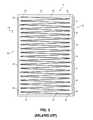
- FIG. 1is a plan view illustrating an embodiment of a touchpad structure
- FIGS. 2-4are plans views illustrating alternative embodiments of touchpad structures.
- FIG. 5is a block diagram illustrating an embodiment of an electronic system having a processing device for detecting a presence of a conductive object.
- FIG. 1illustrates an example of a touchpad structure (or capacitive sensor array) 10 with interleaved conductive traces, or capacitive sensing elements, spaced from each other across a touchpad surface 12 (e.g., a substrate).
- the touchpad structure 10includes pairs of conductive traces 14 - 26 , with each of the pairs including a first conductive trace 28 and a second conductive trace 30 .
- the pairs of conductive traces 14 - 26are arranged in a series of rows, with each row substantially extending along an x-axis of the structure 10 , while the rows are aligned (or stacked) along a y-axis of the structure 10 .
- the first and second conductive tracesare substantially co-planar and made of, for example, indium tin oxide (ITO).
- ITOindium tin oxide
- each of the conductive traces 28 and 30may be connected to a corresponding capacitive sensing pin, and may be implemented within an electronic system as described below.
- each of the conductive traces 28 and 30includes multiple sub-traces (or fingers or members) 32 that extend towards and interleaved with the sub-traces 32 of the other conductive trace within the same pair of conductive traces.
- the sub-traces 32are tapered in such a way that the width of the sub-traces 32 of the first conductive traces 28 is decreased as the sub-traces 32 extend from a first edge (or side) 34 of the structure 10 to a second edge 36 of the structure 10 .
- width of the sub-traces 32 of the second conductive traces 30is decreased as the sub-traces 32 extend from the second edge 36 of the structure 10 to the first edge 34 of the structure 10 .
- the overall width of the first conductive traces 28decreases from the first edge 34 of the structure 10 (or at a first end of the trace 28 ) to the second edge of the structure 10 (or at a second end of the trace 28 ), while the overall width of the second conductive traces 30 decreases from the second edge 36 of the structure 10 (or at a first end of the trace 30 ) to the first edge of the structure 10 (or at a second end of the trace 30 ).
- the capacitance between the conductive traces 28 and 30 and groundvaries and can be detected.
- the two-dimensional position of a stylus or a finger on the touchpad structure 10may be detected by comparing the capacitance variation of each conductive trace 28 and 30 within each pair 14 - 26 , as well as comparing the capacitance variation of the traces 28 and 30 within each pair 14 - 26 to the conductive traces in neighboring pairs.
- a position coordinate along the x-axismay be determined by comparing the capacitance variation between the first conductive trace 28 and the second conductive trace 30 within each of the pairs 14 - 26 of conductive traces. As the object is positioned closer to the first edge 34 of the structure 10 , the capacitance variation of the first conductive trace(s) 28 is increasingly greater than that of the second conductive trace(s) 30 , and vice versa.
- a position coordinate along the y-axismay be determined by comparing the capacitance variation of the traces 28 or 30 in a first pair of traces to the neighboring trace(s) 28 and 30 in an adjacent pair of traces. For example, the determination of the y-axis coordinate may include comparing the capacitance variation of the second trace 30 in conductive trace pair 16 with that of the first trace 28 in conductive trace pair 18 .
- the capacitance variation for the various conductive traces 28 and 30was performed by sequentially scanning all of the first conductive traces 28 (e.g., starting with the first conductive trace 28 in pair 14 and ending with the first conductive trace 28 in pair 26 ), and then sequentially scanning all of the second conductive traces 30 .
- the objectis placed on the touchpad structure 10 (i.e., a “touchdown” event) after the first conductive trace 28 has been scanned for a given pair of traces, but before the second conductive trace 30 for that same pair has been scanned.
- the first conductive trace 28will indicate no signal (or capacitance variation)
- the second conductive trace 30will indicate a signal due to the object.
- an x-axis position at the second edge 36 of the structure 10may be reported, regardless of the actual object location.
- a similar errormay also result when the object is removed from the structure 10 (i.e., a “liftoff” event) after the first conductive trace 28 has been scanned, but before the second conductive trace is scanned. In such an event, an x-axis position at the first edge 34 of the structure 10 may be reported, regardless of actual object location.
- the scanning of the conductive traces 28 and 30is performed in an alternating manner. That is, within each scan cycle, at least some of the second conductive traces 30 are scanned before the scanning of all of the first conductive traces 28 has been completed, and vice versa.
- both conductive traces 28 and 30 in a pair of conductive tracesare scanned before the conductive traces 28 and 30 in the next pair is scanned.
- the first conductive trace 28 in conductive trace pair 14is first scanned, and then the second conductive trace 30 in conductive trace pair 14 is scanned. This process is then sequentially repeated for the remaining conductive trace pairs 16 - 26 .
- a touch “de-bounce”is added. That is, after the first scanning cycle in which an object is detected, no coordinate is reported. Instead, another scanning cycle is conducted immediately. The data from this second scan is then used to determine the initial touchdown coordinate.
- the peak, combined signal strength from the first and second conductive traces 28 and 30 within each pair of conductive traces 14 - 26is monitored.
- a threshold amounte.g., a predetermined percentage of the peak signal strength
- the touch threshold applied to signals on the top and bottom sensor rowsmay be increased when compared to that of the other rows (i.e., signals from the conductive traces at the interior or central portion of the structure 10 ). This reduces the chance that an object covering just one sub-trace 32 of the top most or bottom most conductive trace will lead to a touch being reported.
- sensitivity to a touchis not uniform across conventional touchpad structures, such as that shown in FIG. 1 .
- Prior art implementationssuffer some touch sensitivity variation depending on whether the object is centered over a row (or a column) or between rows.
- the objectwhen an object is in contact near the first edge 34 of the structure 10 , the object causes a relatively strong signal on the first conductive traces 28 that it covers but not on the second conductive traces 30 , and vice versa.
- an object near the central portion of the structure 10will cause a signal on both the first and second conductive traces 28 and 30 .
- the magnitude of this signalis less than the peak sensor signal observed when the object is placed near the first or second edges 34 and 36 since the total signal caused by the finger is split among the left and right sensors. Therefore, if the sensor with the largest signal is used to determine the presence of a touch, the panel will be less sensitive near the vertical center line than near the left or right edges. In this case, a compromise may be used to allow enough sensitivity near the vertical center of the panel without being too sensitive near the left and right edges.
- the peak sensor signal value added to the sensor signal value from the other conductive trace within the same pair of conductive tracesmay be used.
- the conductive trace with the peak valueis the first conductive trace 28 in conductive trace pair 20
- that signal valuemay be added to the signal value of the second conductive trace 30 in conductive trace pair 20 .
- the resultis a total signal strength that is nearly constant across any given row which results in a more uniform touch sensitivity. It should be understood that such a method may be used with traditional single electrode or multi-electrode sensor structures, including those utilizing mutual capacitance sensing.
- the signalis divided between the first conductive trace 28 in pair 16 and the first conductive trace 28 in pair 18 .
- the signal thresholdin order to detect the presence of the object using a single, peak signal, the signal threshold must be lowered in order to overcome a lower signal-to-noise ratio (SNR), which may increase the likelihood of a false object detection. This is particularly true in application where the object is considerably smaller than the sensor elements, such as when a stylus is used.
- SNRsignal-to-noise ratio
- the peak sensor signal value added to the sensor signal value from the adjacent rows of conductive tracesmay be used.
- the conductive trace with the peak valueis the first conductive trace 28 in conductive trace pair 20
- that signal valuemay be added to the signal value of the first conductive trace 28 in conductive trace pairs 18 and 22 .
- the resultis a total signal strength that is nearly constant across any given set of rows which results in a more uniform touch sensitivity.
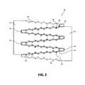
- FIGS. 2 , 3 , and 4illustrate portions of touchpad structures 40 according to other embodiments of the present invention.
- the embodiment shown in FIGS. 2-4includes first conductive traces 42 and second conductive traces 44 that are configured in a manner similar to the “backgammon” structure.
- the first and second conductive traces 42 and 44includes sub-traces 46 .
- the first and second conductive traces 42 and 46also include series of sub-trace protrusions 48 that extend from the sub-traces 46 thereof into the sub-traces of the other conductive trace.
- the sub-trace protrusions 48 on the sub-traces 46 of the first conductive traceextend into the sub-traces 46 of the second conductive trace 44 , and vice versa.
- the sub-trace protrusions 48 of the first conductive trace 42are insulated from the second conductive trace 44 by an insulating material (not specifically shown), while being electrically connected to the first conductive trace 42 .
- the sub-trace protrusions 48 of the second conductive trace 44are insulated from the first conductive trace 42 , while being electrically connected to the second conductive trace 44 .
- the sub-trace protrusions 48are made of the same material, and are integral with, the respective conductive traces.
- the sub-trace protrusions 48 shown in FIG. 2are substantially linear, while those in FIG. 3 are in the shapes of a triangle.
- the sub-trace protrusions 48are thin metal traces (e.g., having widths of, for example, 4 micrometers ( ⁇ m)).
- the effect of the sub-trace protrusions 48is to reduce the size of the “dead zone” in the middle of the thick end of the sub-traces 46 .
- the ideais that even if the touch area is wholly within the thick end of a triangle, the non-linear edge of each triangle will reduce or eliminate the size of the “dead zone” in which the a touch fails to cause a substantial difference in coupling between triangles when a touch occurs within the “dead zone.”
- a method for operating a capacitive sensing deviceis provided.
- a substrate having a plurality of pairs of conductive traces formed thereonis provided.
- Each of the plurality of pairs of conductive tracesincludes a first conductive trace having at least one sub-trace and a second conductive trace having at least one sub-trace.
- At least one sub-trace of the first conductive traceis interleaved with at least one sub-trace of the second conductive trace.
- Each sub-trace of the first and second conductive traceshas a variable width from a first end to a second end thereof.
- a capacitance variation of a plurality of the first conductive traces and a plurality of the second conductive tracesis measured.
- the capacitance variation of at least some of the second conductive tracesis measured before the capacitance variation for all of the plurality of first conductive traces is measured.
- a position coordinate in a two-dimensional coordinate system on the capacitive sensing deviceis determined based on the measuring a capacitance variation of a plurality of the first conductive traces and a plurality of the second conductive traces.
- a capacitive sensing devicein another embodiment, includes a capacitive sensing array and a processing device.
- the capacitive sensing arrayincludes a substrate and a plurality of pairs of conductive traces formed on the substrate.
- Each of the plurality of pairs of conductive tracesincludes a first conductive trace having at least one sub-trace and a second conductive trace having at least one sub-trace.
- At least one sub-trace of the first conductive traceis interleaved with at least one sub-race of the second conductive trace.
- Each sub-trace of the first and second conductive traceshas a variable width from a first end to a second end thereof.
- the processing deviceis coupled to the capacitive sensing array.
- the processing deviceis configured to measure a capacitance variation of a plurality of the first conductive traces and a plurality of the second conductive traces.
- the capacitance variation of at least some of the second conductive tracesis measured before the capacitance variation for all of the plurality of first conductive traces is measured.
- the processing deviceis also configured to determine position coordinate in a two-dimensional coordinate system on the capacitive sensing device based on the measuring a capacitance variation of a plurality of the first conductive traces and a plurality of the second conductive traces.
- a method for operating a capacitive sensing deviceis provided.
- a substrate having a plurality of pairs of conductive traces formed thereonis provided.
- the plurality of pairs of conductive tracesare arranged in a plurality of rows.
- Each of the plurality of pairs of conductive tracesincludes a first conductive trace having at least one sub-trace and a second conductive trace having at least one sub-trace.
- at least one sub-trace of the first conductive traceis interleaved with at least one sub-trace of the second conductive trace.
- Each sub-trace of the first and second conductive traceshas a variable width from a first end to a second end thereof and are substantially aligned with the plurality of rows.
- a capacitance variation of a plurality of the first conductive traces and a plurality of the second conductive tracesis measured.
- the capacitance variation of at least some of the second conductive tracesis measured before the capacitance variation for all of the plurality of first conductive traces is measured.
- the presence of an object relative to the substrateis determined based on the measuring a capacitance variation of a plurality of the first conductive traces and a plurality of the second conductive traces.
- FIG. 5illustrates a block diagram of one embodiment of an electronic system having a processing device for detecting a presence of a conductive object according to an embodiment of the present invention.
- the electronic system 100includes a processing device 110 , a touch-sensor pad 120 , a touch-sensor slider 130 , touch-sensor buttons 140 , a host processor 150 , an embedded controller 160 , and non-capacitance sensor elements 170 .
- the processing device 110may include analog and/or digital general purpose input/output (“GPIO”) ports 107 .
- the GPIO ports 107may be programmable and may be coupled to a Programmable Interconnect and Logic (“PIL”), which acts as an interconnect between the GPIO ports 107 and a digital block array of the processing device 110 .
- PILProgrammable Interconnect and Logic
- the digital block arraymay be configured to implement a variety of digital logic circuits (e.g., DACs, digital filters, or digital control systems) using, in one embodiment, configurable user modules (“UMs”).
- the digital block arraymay be coupled to a system bus.
- the processing device 110may also include memory, such as random access memory (“RAM”) 105 and program flash 104 .
- the RAM 105may be static RAM (“SRAM”), and the program flash 104 may be a non-volatile storage, which may be used to store firmware (e.g., control algorithms executable by processing core 102 to implement operations described herein).
- the processing device 110may also include a memory controller unit (“MCU”) 103 coupled to memory and the processing core 102 .
- MCUmemory controller unit
- the processing device 110may also include an analog block array.
- the analog block arrayis also coupled to the system bus.
- the analog block arrayalso may be configured to implement a variety of analog circuits (e.g., ADCs or analog filters) using, in one embodiment, configurable UMs.
- the analog block arraymay also be coupled to the GPIO 107 .
- the capacitance sensing circuit 101may be integrated into the processing device 110 .
- the capacitance sensing circuit 101may include analog I/O for coupling to an external component, such as the touch-sensor pad 120 , the touch-sensor slider 130 , the touch-sensor buttons 140 , and/or other devices.
- the capacitance sensing circuit 101 and the processing device 110are described in more detail below.
- the sensing devicemay be a touch screen, a touch-sensor slider 130 , or touch-sensor buttons 140 (e.g., capacitance sensing buttons). In one embodiment, these sensing devices may include one or more capacitive sensors.
- the operations described hereinare not limited to notebook pointer operations, but can include other operations, such as lighting control (dimmer), volume control, graphic equalizer control, speed control, or other control operations requiring gradual or discrete adjustments. It should also be noted that these embodiments of capacitive sensing implementations may be used in conjunction with non-capacitive sensing elements, including but not limited to pick buttons, sliders (ex. display brightness and contrast), scroll-wheels, multi-media control (ex. volume, track advance, etc) handwriting recognition and numeric keypad operation.
- the electronic system 100includes a touch-sensor pad 120 coupled to the processing device 110 via bus 121 .
- the touch-sensor pad 120may include a multi-dimension sensor array.
- the multi-dimension sensor arrayincludes multiple sensor elements, organized as rows and columns, such as the sensor arrays described above and shown in FIGS. 1 , 2 , 3 , and 4 .
- the electronic system 100includes a touch-sensor slider 130 coupled to the processing device 110 via bus 131 .
- the touch-sensor slider 130may include a single-dimension sensor array.
- the single-dimension sensor arrayincludes multiple sensor elements, organized as rows, or alternatively, as columns.
- the electronic system 100includes touch-sensor buttons 140 coupled to the processing device 110 via bus 141 .
- the touch-sensor buttons 140may include a single-dimension or multi-dimension sensor array.
- the single- or multi-dimension sensor arraymay include multiple sensor elements.
- the sensor elementsmay be coupled together to detect a presence of a conductive object over the entire surface of the sensing device.
- the touch-sensor buttons 140may have a single sensor element to detect the presence of the conductive object.
- the touch-sensor buttons 140may include a capacitive sensor element.
- the capacitive sensor elementsmay be used as non-contact sensor elements. These sensor elements, when protected by an insulating layer, offer resistance to severe environments.
- the electronic system 100may include any combination of one or more of the touch-sensor pad 120 , the touch-sensor slider 130 , and/or the touch-sensor button 140 .
- the electronic system 100may also include non-capacitance sensor elements 170 coupled to the processing device 110 via bus 171 .
- the non-capacitance sensor elements 170may include buttons, light emitting diodes (“LEDs”), and other user interface devices, such as a mouse, a keyboard, or other functional keys that do not require capacitance sensing.
- buses 171 , 141 , 131 , and 121may be a single bus. Alternatively, these buses may be configured into any combination of one or more separate buses.
- the processing device 110may include internal oscillator/clocks 106 and a communication block (“COM”) 108 .
- the oscillator/clocks 106provides clock signals to one or more of the components of the processing device 110 .
- the communication block 108may be used to communicate with an external component, such as a host processor 150 , via host interface (“I/F”) line 151 .
- the processing block 110may also be coupled to embedded controller 160 to communicate with the external components, such as host 150 .
- the processing device 110is configured to communicate with the embedded controller 160 or the host 150 to send and/or receive data.
- the processing device 110may reside on a common carrier substrate such as, for example, an integrated circuit (“IC”) die substrate, a multi-chip module substrate, or the like.
- the components of the processing device 110may be one or more separate integrated circuits and/or discrete components.
- the processing device 110may be a Programmable System on a Chip (“PSoCTM”) processing device, manufactured by Cypress Semiconductor Corporation, San Jose, Calif.
- the processing device 110may be one or more other processing devices known by those of ordinary skill in the art, such as a microprocessor or central processing unit, a controller, special-purpose processor, digital signal processor (“DSP”), an application specific integrated circuit (“ASIC”), a field programmable gate array (“FPGA”), or the like.
- DSPdigital signal processor
- ASICapplication specific integrated circuit
- FPGAfield programmable gate array
- processing device 110may also be done in the host.
- the capacitance sensing circuit 101may be integrated into the IC of the processing device 110 , or alternatively, in a separate IC. Alternatively, descriptions of the capacitance sensing circuit 101 may be generated and compiled for incorporation into other integrated circuits. For example, behavioral level code describing the capacitance sensing circuit 101 , or portions thereof, may be generated using a hardware descriptive language, such as VHDL or Verilog, and stored to a machine-accessible medium (e.g., CD-ROM, hard disk, floppy disk, etc.). Furthermore, the behavioral level code can be compiled into register transfer level (“RTL”) code, a netlist, or even a circuit layout and stored to a machine-accessible medium. The behavioral level code, the RTL code, the netlist, and the circuit layout all represent various levels of abstraction to describe the capacitance sensing circuit 101 .
- a hardware descriptive languagesuch as VHDL or Verilog
- the components of the electronic system 100may include all the components described above. Alternatively, the electronic system 100 may include only some of the components described above.
- the electronic system 100may be used in a notebook computer.
- the electronic system 100may be used in other applications, such as a mobile handset, a personal data assistant (“PDA”), a keyboard, a television, a remote control, a monitor, a handheld multi-media device, a handheld video player, a handheld gaming device, or a control panel.
- PDApersonal data assistant
- the conductive object in this caseis a finger
- this techniquemay be applied to any conductive object, for example, a conductive door switch, position sensor, or conductive pen in a stylus tracking system.
Landscapes
- Engineering & Computer Science (AREA)
- General Engineering & Computer Science (AREA)
- Theoretical Computer Science (AREA)
- Human Computer Interaction (AREA)
- Physics & Mathematics (AREA)
- General Physics & Mathematics (AREA)
- Quality & Reliability (AREA)
- Position Input By Displaying (AREA)
Abstract
Description
Claims (20)
Priority Applications (1)
| Application Number | Priority Date | Filing Date | Title |
|---|---|---|---|
| US13/339,822US8692799B1 (en) | 2011-07-05 | 2011-12-29 | Single layer multi-touch capacitive sensor |
Applications Claiming Priority (2)
| Application Number | Priority Date | Filing Date | Title |
|---|---|---|---|
| US201161504471P | 2011-07-05 | 2011-07-05 | |
| US13/339,822US8692799B1 (en) | 2011-07-05 | 2011-12-29 | Single layer multi-touch capacitive sensor |
Publications (1)
| Publication Number | Publication Date |
|---|---|
| US8692799B1true US8692799B1 (en) | 2014-04-08 |
Family
ID=50391827
Family Applications (1)
| Application Number | Title | Priority Date | Filing Date |
|---|---|---|---|
| US13/339,822Expired - Fee RelatedUS8692799B1 (en) | 2011-07-05 | 2011-12-29 | Single layer multi-touch capacitive sensor |
Country Status (1)
| Country | Link |
|---|---|
| US (1) | US8692799B1 (en) |
Cited By (11)
| Publication number | Priority date | Publication date | Assignee | Title |
|---|---|---|---|---|
| US20140078074A1 (en)* | 2012-09-20 | 2014-03-20 | Samsung Electro-Mechanics Co., Ltd. | Touch panel |
| US8873743B1 (en) | 2006-05-18 | 2014-10-28 | Cypress Semiconductor Corporation | Tapered capsense structure |
| US20150061704A1 (en)* | 2013-08-30 | 2015-03-05 | Mstar Semiconductor, Inc. | Sensing method and sensing apparatus for sensing electrode cluster |
| US20150193047A1 (en)* | 2013-09-10 | 2015-07-09 | Cypress Semiconductor Corporation | Interleaving sense elements of a capacitive-sense array |
| US9612265B1 (en) | 2011-09-23 | 2017-04-04 | Cypress Semiconductor Corporation | Methods and apparatus to detect a conductive object |
| WO2018044957A1 (en)* | 2016-08-30 | 2018-03-08 | Tactual Labs Co. | Capacitive sensor |
| US10043960B2 (en)* | 2011-11-15 | 2018-08-07 | Cree, Inc. | Light emitting diode (LED) packages and related methods |
| US10054396B2 (en)* | 2013-11-18 | 2018-08-21 | Richard George Hovsepian | Flush switch for handgun accessory |
| US10228808B2 (en)* | 2009-10-26 | 2019-03-12 | Atmel Corporation | Sense electrode design |
| US10372325B2 (en) | 2014-10-16 | 2019-08-06 | Huawei Technologies Co., Ltd. | Electromyographic based touch interaction processing method, device, and system |
| US10876817B2 (en)* | 2013-11-18 | 2020-12-29 | Richard George Hovsepian | Handgun laser sight with passive switch |
Citations (37)
| Publication number | Priority date | Publication date | Assignee | Title |
|---|---|---|---|---|
| US4087625A (en) | 1976-12-29 | 1978-05-02 | International Business Machines Corporation | Capacitive two dimensional tablet with single conductive layer |
| US4264903A (en) | 1978-06-12 | 1981-04-28 | General Electric Company | Capacitive touch control and display |
| US4622437A (en) | 1984-11-29 | 1986-11-11 | Interaction Systems, Inc. | Method and apparatus for improved electronic touch mapping |
| US4659874A (en) | 1985-09-23 | 1987-04-21 | Sanders Associates, Inc. | X-Y position sensor |
| US4680430A (en) | 1984-02-29 | 1987-07-14 | Fujitsu Limited | Coordinate detecting apparatus |
| US4705919A (en) | 1985-02-21 | 1987-11-10 | Dhawan Satish K | Electrostatic pattern-coupled digitizer |
| US4952757A (en) | 1989-11-15 | 1990-08-28 | Summagraphics Corporation | Low-power electromagnetic digitizer tablet |
| US4999462A (en) | 1989-10-06 | 1991-03-12 | Summagraphics Corporation | Position determining and digitizing method and device |
| US5305017A (en) | 1989-08-16 | 1994-04-19 | Gerpheide George E | Methods and apparatus for data input |
| US5856937A (en) | 1996-11-22 | 1999-01-05 | Ma Laboratories, Inc. | Processor module with dual-bank SRAM cache having shared capacitors and R-C elements integrated into the module substrate |
| US5869790A (en) | 1995-08-16 | 1999-02-09 | Alps Electric Co., Ltd. | Coordinate input apparatus having orthogonal electrodes on opposite surfaces of a dielectric substrate and through-hole connections and manufacturing method thereof |
| US6147680A (en) | 1997-06-03 | 2000-11-14 | Koa T&T Corporation | Touchpad with interleaved traces |
| US6188391B1 (en) | 1998-07-09 | 2001-02-13 | Synaptics, Inc. | Two-layer capacitive touchpad and method of making same |
| US6222522B1 (en) | 1998-09-18 | 2001-04-24 | Interval Research Corporation | Baton and X, Y, Z, position sensor |
| US6239790B1 (en)* | 1996-08-05 | 2001-05-29 | Interlink Electronics | Force sensing semiconductive touchpad |
| US6297811B1 (en) | 1999-06-02 | 2001-10-02 | Elo Touchsystems, Inc. | Projective capacitive touchscreen |
| US6353200B2 (en) | 1998-05-04 | 2002-03-05 | Inocon Technologie Gesellschaft M.B.H. | Method for the partial fusion of objects |
| US6380931B1 (en) | 1992-06-08 | 2002-04-30 | Synaptics Incorporated | Object position detector with edge motion feature and gesture recognition |
| US20040239650A1 (en) | 2003-06-02 | 2004-12-02 | Mackey Bob Lee | Sensor patterns for a capacitive sensing apparatus |
| US6879930B2 (en) | 2001-03-30 | 2005-04-12 | Microsoft Corporation | Capacitance touch slider |
| US6888538B2 (en) | 1994-05-14 | 2005-05-03 | Synaptics (Uk) Limited | Position sensor |
| US20060097991A1 (en) | 2004-05-06 | 2006-05-11 | Apple Computer, Inc. | Multipoint touchscreen |
| US20060278444A1 (en) | 2003-06-14 | 2006-12-14 | Binstead Ronald P | Touch technology |
| US20070247443A1 (en) | 2006-04-25 | 2007-10-25 | Harald Philipp | Hybrid Capacitive Touch Screen Element |
| US20070257894A1 (en) | 2006-05-05 | 2007-11-08 | Harald Philipp | Touch Screen Element |
| US20070271399A1 (en)* | 2006-05-18 | 2007-11-22 | Cypress Semiconductor Corporation | Tapered capsense structure |
| US7368921B2 (en)* | 2006-02-10 | 2008-05-06 | Milliken & Company | Printed capacitive sensor |
| US7382139B2 (en) | 2004-06-03 | 2008-06-03 | Synaptics Incorporated | One layer capacitive sensing apparatus having varying width sensing elements |
| US7436395B2 (en)* | 2004-02-17 | 2008-10-14 | Elan Microelectronics Corporation | Simplified capacitive touchpad and method thereof |
| US7548073B2 (en) | 2006-01-30 | 2009-06-16 | Synaptics Incorporated | Capacitive sensing apparatus designs |
| US7609125B2 (en)* | 2006-10-13 | 2009-10-27 | Avago Technologies Enterprise IP (Singapore) Pte. Ltd. | System, device and method for reducing cross-talk in differential signal conductor pairs |
| US7876309B2 (en) | 2006-05-18 | 2011-01-25 | Cypress Semiconductor Corporation | Toothed slider |
| US20110210935A1 (en)* | 2010-03-01 | 2011-09-01 | Cando Corporation | Sensory structure of capacitive touch panel and capacitive touch panel having the same |
| US20110242001A1 (en)* | 2010-03-30 | 2011-10-06 | Flextronics Ap, Llc | Simplified Mechanical Design for an Acoustic Touch Screen |
| US20120046887A1 (en)* | 2006-07-31 | 2012-02-23 | Xiaoping Jiang | Two-pin coupling slider |
| US20120313880A1 (en)* | 2008-02-28 | 2012-12-13 | 3M Innovative Properties Company | Touch screen sensor with low visibility conductors |
| US8373664B2 (en)* | 2006-12-18 | 2013-02-12 | Cypress Semiconductor Corporation | Two circuit board touch-sensor device |
- 2011
- 2011-12-29USUS13/339,822patent/US8692799B1/ennot_activeExpired - Fee Related
Patent Citations (42)
| Publication number | Priority date | Publication date | Assignee | Title |
|---|---|---|---|---|
| US4087625A (en) | 1976-12-29 | 1978-05-02 | International Business Machines Corporation | Capacitive two dimensional tablet with single conductive layer |
| US4264903A (en) | 1978-06-12 | 1981-04-28 | General Electric Company | Capacitive touch control and display |
| US4680430A (en) | 1984-02-29 | 1987-07-14 | Fujitsu Limited | Coordinate detecting apparatus |
| US4622437A (en) | 1984-11-29 | 1986-11-11 | Interaction Systems, Inc. | Method and apparatus for improved electronic touch mapping |
| US4705919A (en) | 1985-02-21 | 1987-11-10 | Dhawan Satish K | Electrostatic pattern-coupled digitizer |
| US4659874A (en) | 1985-09-23 | 1987-04-21 | Sanders Associates, Inc. | X-Y position sensor |
| US5305017A (en) | 1989-08-16 | 1994-04-19 | Gerpheide George E | Methods and apparatus for data input |
| US4999462A (en) | 1989-10-06 | 1991-03-12 | Summagraphics Corporation | Position determining and digitizing method and device |
| US4952757A (en) | 1989-11-15 | 1990-08-28 | Summagraphics Corporation | Low-power electromagnetic digitizer tablet |
| US6380931B1 (en) | 1992-06-08 | 2002-04-30 | Synaptics Incorporated | Object position detector with edge motion feature and gesture recognition |
| US6888538B2 (en) | 1994-05-14 | 2005-05-03 | Synaptics (Uk) Limited | Position sensor |
| US5869790A (en) | 1995-08-16 | 1999-02-09 | Alps Electric Co., Ltd. | Coordinate input apparatus having orthogonal electrodes on opposite surfaces of a dielectric substrate and through-hole connections and manufacturing method thereof |
| US6239790B1 (en)* | 1996-08-05 | 2001-05-29 | Interlink Electronics | Force sensing semiconductive touchpad |
| US5856937A (en) | 1996-11-22 | 1999-01-05 | Ma Laboratories, Inc. | Processor module with dual-bank SRAM cache having shared capacitors and R-C elements integrated into the module substrate |
| US6147680A (en) | 1997-06-03 | 2000-11-14 | Koa T&T Corporation | Touchpad with interleaved traces |
| US6353200B2 (en) | 1998-05-04 | 2002-03-05 | Inocon Technologie Gesellschaft M.B.H. | Method for the partial fusion of objects |
| US6188391B1 (en) | 1998-07-09 | 2001-02-13 | Synaptics, Inc. | Two-layer capacitive touchpad and method of making same |
| US6222522B1 (en) | 1998-09-18 | 2001-04-24 | Interval Research Corporation | Baton and X, Y, Z, position sensor |
| US6297811B1 (en) | 1999-06-02 | 2001-10-02 | Elo Touchsystems, Inc. | Projective capacitive touchscreen |
| US6879930B2 (en) | 2001-03-30 | 2005-04-12 | Microsoft Corporation | Capacitance touch slider |
| US7129935B2 (en) | 2003-06-02 | 2006-10-31 | Synaptics Incorporated | Sensor patterns for a capacitive sensing apparatus |
| US20040239650A1 (en) | 2003-06-02 | 2004-12-02 | Mackey Bob Lee | Sensor patterns for a capacitive sensing apparatus |
| US20060278444A1 (en) | 2003-06-14 | 2006-12-14 | Binstead Ronald P | Touch technology |
| US7436395B2 (en)* | 2004-02-17 | 2008-10-14 | Elan Microelectronics Corporation | Simplified capacitive touchpad and method thereof |
| US20060097991A1 (en) | 2004-05-06 | 2006-05-11 | Apple Computer, Inc. | Multipoint touchscreen |
| US7663607B2 (en) | 2004-05-06 | 2010-02-16 | Apple Inc. | Multipoint touchscreen |
| US7382139B2 (en) | 2004-06-03 | 2008-06-03 | Synaptics Incorporated | One layer capacitive sensing apparatus having varying width sensing elements |
| US7548073B2 (en) | 2006-01-30 | 2009-06-16 | Synaptics Incorporated | Capacitive sensing apparatus designs |
| US7368921B2 (en)* | 2006-02-10 | 2008-05-06 | Milliken & Company | Printed capacitive sensor |
| US20070247443A1 (en) | 2006-04-25 | 2007-10-25 | Harald Philipp | Hybrid Capacitive Touch Screen Element |
| US20100271330A1 (en)* | 2006-05-05 | 2010-10-28 | Atmel Corporation | Touch screen element |
| US20070257894A1 (en) | 2006-05-05 | 2007-11-08 | Harald Philipp | Touch Screen Element |
| US20070271399A1 (en)* | 2006-05-18 | 2007-11-22 | Cypress Semiconductor Corporation | Tapered capsense structure |
| US7876309B2 (en) | 2006-05-18 | 2011-01-25 | Cypress Semiconductor Corporation | Toothed slider |
| US8121283B2 (en)* | 2006-05-18 | 2012-02-21 | Cypress Semiconductor Corporation | Tapered capacitive sensing structure |
| US20120043141A1 (en) | 2006-05-18 | 2012-02-23 | Cypress Semiconductor Corporation | Toothed Slider |
| US20120046887A1 (en)* | 2006-07-31 | 2012-02-23 | Xiaoping Jiang | Two-pin coupling slider |
| US7609125B2 (en)* | 2006-10-13 | 2009-10-27 | Avago Technologies Enterprise IP (Singapore) Pte. Ltd. | System, device and method for reducing cross-talk in differential signal conductor pairs |
| US8373664B2 (en)* | 2006-12-18 | 2013-02-12 | Cypress Semiconductor Corporation | Two circuit board touch-sensor device |
| US20120313880A1 (en)* | 2008-02-28 | 2012-12-13 | 3M Innovative Properties Company | Touch screen sensor with low visibility conductors |
| US20110210935A1 (en)* | 2010-03-01 | 2011-09-01 | Cando Corporation | Sensory structure of capacitive touch panel and capacitive touch panel having the same |
| US20110242001A1 (en)* | 2010-03-30 | 2011-10-06 | Flextronics Ap, Llc | Simplified Mechanical Design for an Acoustic Touch Screen |
Non-Patent Citations (25)
| Title |
|---|
| Chapweske, Adam; "The PS/2 Mouse Interface," PS/2 Mouse Interfacing, 2001, retrieved on May 18, 2006; 11 pages. |
| Cypress Semiconductor Corporation, "CY8C21x34 Data Sheet," CSR User Module, CSR V.1.0; Oct. 6, 2005; 36 pages. |
| Hal Philipp, "Charge Transfer Sensing", Spread Spectrum Sensor Technology Blazes New Applications, 1997, 9 pages. |
| U.S. Appl. No. 11/437,507: "Tapered Capacitive Sensing Structure" Tao Peng et al., filed May 18, 2006; 50 pages. |
| U.S. Appl. No. 11/437,518: "Toothed Slider" Jiang XiaoPing et al., filed May 18, 2006; 45 pages. |
| U.S. Appl. No. 13/012,750: "Toothed Slider," Jiang XiaoPing, filed Jan. 24, 2011; 46 pages. |
| USPTO Advisory Action for U.S. Appl. No. 11/437,507 dated Jul. 12, 2010; 2 pages. |
| USPTO Final Rejection for U.S. Appl. No. 11/437,507 dated Apr. 15, 2010; 5 pages. |
| USPTO Final Rejection for U.S. Appl. No. 11/437,507 dated Nov. 14, 2008; 8 pages. |
| USPTO Final Rejection for U.S. Appl. No. 13/012,750 dated Jan. 23, 2013; 14 pages. |
| USPTO Non Final Rejection for U.S. Appl. No. 13/304,301 dated Sep. 26, 2013; 7 pages. |
| USPTO Non-Final Rejection for U.S. Appl. No. 11/437,507 dated Apr. 8, 2008; 5 pages. |
| USPTO Non-Final Rejection for U.S. Appl. No. 11/437,507 dated Feb. 23, 2009; 9 pages. |
| USPTO Non-Final Rejection for U.S. Appl. No. 11/437,507 dated Jun. 28, 2011; 5 pages. |
| USPTO Non-Final Rejection for U.S. Appl. No. 11/437,507 dated Oct. 29, 2009; 5 pages. |
| USPTO Non-Final Rejection for U.S. Appl. No. 11/437,507 dated Sep. 23, 2010; 6 pages. |
| USPTO Non-Final Rejection for U.S. Appl. No. 11/437,518 dated Aug. 18, 2009; 10 pages. |
| USPTO Non-Final Rejection for U.S. Appl. No. 13/012,750 dated Sep. 11, 2012; 13 pages. |
| USPTO Notice of Allowance for U.S. Appl. No. 11/437,507 dated Dec. 23, 2011; 7 pages. |
| USPTO Notice of Allowance for U.S. Appl. No. 11/437,507 dated Mar. 14, 2011; 7 pages. |
| USPTO Notice of Allowance for U.S. Appl. No. 11/437,507 dated May 2, 2011; 5 pages. |
| USPTO Notice of Allowance for U.S. Appl. No. 11/437,518 dated Feb. 23, 2010; 6 pages. |
| USPTO Notice of Allowance for U.S. Appl. No. 11/437,518 dated Sep. 17, 2010; 4 pages. |
| USPTO Notice of Allowance for U.S. Appl. No. 13/012,750 dated Mar. 14, 2013; 5 pages. |
| USPTO Requirement for Restriction/Election for U.S. Appl. No. 11/437,518 dated Apr. 21, 2009; 6 pages. |
Cited By (18)
| Publication number | Priority date | Publication date | Assignee | Title |
|---|---|---|---|---|
| US8873743B1 (en) | 2006-05-18 | 2014-10-28 | Cypress Semiconductor Corporation | Tapered capsense structure |
| US10795523B2 (en) | 2009-10-26 | 2020-10-06 | Neodrón Limited | Sense electrode design |
| US10338759B1 (en) | 2009-10-26 | 2019-07-02 | Neodrón Limited | Sense electrode design |
| US10228808B2 (en)* | 2009-10-26 | 2019-03-12 | Atmel Corporation | Sense electrode design |
| US9612265B1 (en) | 2011-09-23 | 2017-04-04 | Cypress Semiconductor Corporation | Methods and apparatus to detect a conductive object |
| US10043960B2 (en)* | 2011-11-15 | 2018-08-07 | Cree, Inc. | Light emitting diode (LED) packages and related methods |
| US20140078074A1 (en)* | 2012-09-20 | 2014-03-20 | Samsung Electro-Mechanics Co., Ltd. | Touch panel |
| US9489084B2 (en)* | 2013-08-30 | 2016-11-08 | Mstar Semiconductor, Inc. | Sensing method and sensing apparatus for sensing electrode cluster |
| US20150061704A1 (en)* | 2013-08-30 | 2015-03-05 | Mstar Semiconductor, Inc. | Sensing method and sensing apparatus for sensing electrode cluster |
| US9563318B2 (en)* | 2013-09-10 | 2017-02-07 | Monterey Research, Llc | Interleaving conductive elements of a capacitive-sense array |
| US20150193047A1 (en)* | 2013-09-10 | 2015-07-09 | Cypress Semiconductor Corporation | Interleaving sense elements of a capacitive-sense array |
| US10054396B2 (en)* | 2013-11-18 | 2018-08-21 | Richard George Hovsepian | Flush switch for handgun accessory |
| US20180347944A1 (en)* | 2013-11-18 | 2018-12-06 | Richard George Hovsepian | Flush Switch for Handgun Accessory |
| US10876817B2 (en)* | 2013-11-18 | 2020-12-29 | Richard George Hovsepian | Handgun laser sight with passive switch |
| US10372325B2 (en) | 2014-10-16 | 2019-08-06 | Huawei Technologies Co., Ltd. | Electromyographic based touch interaction processing method, device, and system |
| WO2018044957A1 (en)* | 2016-08-30 | 2018-03-08 | Tactual Labs Co. | Capacitive sensor |
| US10386975B2 (en) | 2016-08-30 | 2019-08-20 | Tactual Labs Co. | Capacitive sensor |
| US10503331B2 (en) | 2016-08-30 | 2019-12-10 | Tactual Labs Co. | Single sided capacitive sensor |
Similar Documents
| Publication | Publication Date | Title |
|---|---|---|
| US8692799B1 (en) | Single layer multi-touch capacitive sensor | |
| US11995250B2 (en) | Active stylus and capacitive position detection system having touch object detecting mode and stylus detecting mode | |
| US9684418B1 (en) | Self and mutual capacitance measurement in a touch screen | |
| US8982097B1 (en) | Water rejection and wet finger tracking algorithms for truetouch panels and self capacitance touch sensors | |
| US9116581B2 (en) | Edge accuracy in a capacitive sense array | |
| US9563318B2 (en) | Interleaving conductive elements of a capacitive-sense array | |
| US8773386B2 (en) | Methods and apparatus to scan a targeted portion of an input device to detect a presence | |
| US8988086B1 (en) | Capacitive sensor array with pattern variation | |
| US9151790B1 (en) | Sensor pattern with inactive electrodes in transmit (TX) layer for mutual capacitance | |
| US20160004361A1 (en) | Barrier Electrode Driven By An Excitation Signal | |
| US9594462B2 (en) | Uniform signals from non-uniform patterns of electrodes | |
| KR101780296B1 (en) | Mutual capacitance sensing array | |
| US8970796B2 (en) | Field-line repeater (FLR) structure of a sense array | |
| US10613695B2 (en) | Integrated touch sensing and force sensing in a touch detection device | |
| US8593431B1 (en) | Edge positioning accuracy in a mutual capacitive sense array | |
| US8903679B2 (en) | Accuracy in a capacitive sense array | |
| US9507454B1 (en) | Enhanced linearity of gestures on a touch-sensitive surface | |
| KR20140075679A (en) | Improved edge accuracy in a capacitive sense array | |
| US12443293B2 (en) | Stylus detection system having touch object detecting mode and stylus detecting mode |
Legal Events
| Date | Code | Title | Description |
|---|---|---|---|
| AS | Assignment | Owner name:CYPRESS SEMICONDUCTOR CORPORATION, CALIFORNIA Free format text:ASSIGNMENT OF ASSIGNORS INTEREST;ASSIGNORS:LANDRY, GREGORY;KOLOKOWSKY, STEVE;WRIGHT, DAVID G.;REEL/FRAME:027459/0693 Effective date:20111222 | |
| AS | Assignment | Owner name:MORGAN STANLEY SENIOR FUNDING, INC., NEW YORK Free format text:PATENT SECURITY AGREEMENT;ASSIGNOR:CYPRESS SEMICONDUCTOR CORPORATION;REEL/FRAME:028863/0870 Effective date:20120822 | |
| AS | Assignment | Owner name:MORGAN STANLEY SENIOR FUNDING, INC., NEW YORK Free format text:SECURITY INTEREST;ASSIGNORS:CYPRESS SEMICONDUCTOR CORPORATION;SPANSION LLC;REEL/FRAME:035240/0429 Effective date:20150312 | |
| AS | Assignment | Owner name:CYPRESS SEMICONDUCTOR CORPORATION, CALIFORNIA Free format text:PARTIAL RELEASE OF SECURITY INTEREST IN PATENTS;ASSIGNOR:MORGAN STANLEY SENIOR FUNDING, INC., AS COLLATERAL AGENT;REEL/FRAME:039708/0001 Effective date:20160811 Owner name:SPANSION LLC, CALIFORNIA Free format text:PARTIAL RELEASE OF SECURITY INTEREST IN PATENTS;ASSIGNOR:MORGAN STANLEY SENIOR FUNDING, INC., AS COLLATERAL AGENT;REEL/FRAME:039708/0001 Effective date:20160811 | |
| FEPP | Fee payment procedure | Free format text:PAYOR NUMBER ASSIGNED (ORIGINAL EVENT CODE: ASPN); ENTITY STATUS OF PATENT OWNER: LARGE ENTITY | |
| AS | Assignment | Owner name:MONTEREY RESEARCH, LLC, CALIFORNIA Free format text:ASSIGNMENT OF ASSIGNORS INTEREST;ASSIGNOR:CYPRESS SEMICONDUCTOR CORPORATION;REEL/FRAME:040911/0238 Effective date:20160811 | |
| FEPP | Fee payment procedure | Free format text:MAINTENANCE FEE REMINDER MAILED (ORIGINAL EVENT CODE: REM.) | |
| LAPS | Lapse for failure to pay maintenance fees | Free format text:PATENT EXPIRED FOR FAILURE TO PAY MAINTENANCE FEES (ORIGINAL EVENT CODE: EXP.) | |
| STCH | Information on status: patent discontinuation | Free format text:PATENT EXPIRED DUE TO NONPAYMENT OF MAINTENANCE FEES UNDER 37 CFR 1.362 | |
| FP | Lapsed due to failure to pay maintenance fee | Effective date:20180408 | |
| AS | Assignment | Owner name:MORGAN STANLEY SENIOR FUNDING, INC., NEW YORK Free format text:CORRECTIVE ASSIGNMENT TO CORRECT THE 8647899 PREVIOUSLY RECORDED ON REEL 035240 FRAME 0429. ASSIGNOR(S) HEREBY CONFIRMS THE SECURITY INTERST;ASSIGNORS:CYPRESS SEMICONDUCTOR CORPORATION;SPANSION LLC;REEL/FRAME:058002/0470 Effective date:20150312 |