US8692261B2 - Light emitting device grown on a relaxed layer - Google Patents
Light emitting device grown on a relaxed layerDownload PDFInfo
- Publication number
- US8692261B2 US8692261B2US12/783,197US78319710AUS8692261B2US 8692261 B2US8692261 B2US 8692261B2US 78319710 AUS78319710 AUS 78319710AUS 8692261 B2US8692261 B2US 8692261B2
- Authority
- US
- United States
- Prior art keywords
- semiconductor layer
- layer
- lattice constant
- light emitting
- semiconductor
- Prior art date
- Legal status (The legal status is an assumption and is not a legal conclusion. Google has not performed a legal analysis and makes no representation as to the accuracy of the status listed.)
- Active, expires
Links
Images


Classifications
- H—ELECTRICITY
- H10—SEMICONDUCTOR DEVICES; ELECTRIC SOLID-STATE DEVICES NOT OTHERWISE PROVIDED FOR
- H10H—INORGANIC LIGHT-EMITTING SEMICONDUCTOR DEVICES HAVING POTENTIAL BARRIERS
- H10H20/00—Individual inorganic light-emitting semiconductor devices having potential barriers, e.g. light-emitting diodes [LED]
- H10H20/01—Manufacture or treatment
- H10H20/011—Manufacture or treatment of bodies, e.g. forming semiconductor layers
- H10H20/013—Manufacture or treatment of bodies, e.g. forming semiconductor layers having light-emitting regions comprising only Group III-V materials
- H10H20/0137—Manufacture or treatment of bodies, e.g. forming semiconductor layers having light-emitting regions comprising only Group III-V materials the light-emitting regions comprising nitride materials
- H—ELECTRICITY
- H10—SEMICONDUCTOR DEVICES; ELECTRIC SOLID-STATE DEVICES NOT OTHERWISE PROVIDED FOR
- H10H—INORGANIC LIGHT-EMITTING SEMICONDUCTOR DEVICES HAVING POTENTIAL BARRIERS
- H10H20/00—Individual inorganic light-emitting semiconductor devices having potential barriers, e.g. light-emitting diodes [LED]
- H10H20/01—Manufacture or treatment
- H10H20/011—Manufacture or treatment of bodies, e.g. forming semiconductor layers
- H10H20/018—Bonding of wafers
- H—ELECTRICITY
- H10—SEMICONDUCTOR DEVICES; ELECTRIC SOLID-STATE DEVICES NOT OTHERWISE PROVIDED FOR
- H10H—INORGANIC LIGHT-EMITTING SEMICONDUCTOR DEVICES HAVING POTENTIAL BARRIERS
- H10H20/00—Individual inorganic light-emitting semiconductor devices having potential barriers, e.g. light-emitting diodes [LED]
- H10H20/80—Constructional details
- H10H20/81—Bodies
- H10H20/815—Bodies having stress relaxation structures, e.g. buffer layers
- H—ELECTRICITY
- H10—SEMICONDUCTOR DEVICES; ELECTRIC SOLID-STATE DEVICES NOT OTHERWISE PROVIDED FOR
- H10H—INORGANIC LIGHT-EMITTING SEMICONDUCTOR DEVICES HAVING POTENTIAL BARRIERS
- H10H20/00—Individual inorganic light-emitting semiconductor devices having potential barriers, e.g. light-emitting diodes [LED]
- H10H20/80—Constructional details
- H10H20/81—Bodies
- H10H20/822—Materials of the light-emitting regions
- H10H20/824—Materials of the light-emitting regions comprising only Group III-V materials, e.g. GaP
- H10H20/825—Materials of the light-emitting regions comprising only Group III-V materials, e.g. GaP containing nitrogen, e.g. GaN
- H—ELECTRICITY
- H01—ELECTRIC ELEMENTS
- H01L—SEMICONDUCTOR DEVICES NOT COVERED BY CLASS H10
- H01L21/00—Processes or apparatus adapted for the manufacture or treatment of semiconductor or solid state devices or of parts thereof
- H01L21/02—Manufacture or treatment of semiconductor devices or of parts thereof
- H01L21/02104—Forming layers
- H01L21/02365—Forming inorganic semiconducting materials on a substrate
- H01L21/02436—Intermediate layers between substrates and deposited layers
- H01L21/02439—Materials
- H01L21/02455—Group 13/15 materials
- H01L21/02458—Nitrides
- H—ELECTRICITY
- H01—ELECTRIC ELEMENTS
- H01L—SEMICONDUCTOR DEVICES NOT COVERED BY CLASS H10
- H01L21/00—Processes or apparatus adapted for the manufacture or treatment of semiconductor or solid state devices or of parts thereof
- H01L21/02—Manufacture or treatment of semiconductor devices or of parts thereof
- H01L21/02104—Forming layers
- H01L21/02365—Forming inorganic semiconducting materials on a substrate
- H01L21/02436—Intermediate layers between substrates and deposited layers
- H01L21/02494—Structure
- H01L21/02496—Layer structure
- H01L21/02505—Layer structure consisting of more than two layers
- H—ELECTRICITY
- H01—ELECTRIC ELEMENTS
- H01L—SEMICONDUCTOR DEVICES NOT COVERED BY CLASS H10
- H01L2924/00—Indexing scheme for arrangements or methods for connecting or disconnecting semiconductor or solid-state bodies as covered by H01L24/00
- H01L2924/0001—Technical content checked by a classifier
- H01L2924/0002—Not covered by any one of groups H01L24/00, H01L24/00 and H01L2224/00
Definitions
- the present inventionrelates to a semiconductor light emitting device grown on a semiconductor layer that is at least partially relaxed.
- LEDslight emitting diodes
- RCLEDsresonant cavity light emitting diodes
- VCSELsvertical cavity laser diodes
- edge emitting lasersare among the most efficient light sources currently available.
- Materials systems currently of interest in the manufacture of high-brightness light emitting devices capable of operation across the visible spectruminclude Group III-V semiconductors, particularly binary, ternary, and quaternary alloys of gallium, aluminum, indium, and nitrogen, also referred to as III-nitride materials.
- III-nitride light emitting devicesare fabricated by epitaxially growing a stack of semiconductor layers of different compositions and dopant concentrations on a sapphire, silicon carbide, III-nitride, or other suitable substrate by metal-organic chemical vapor deposition (MOCVD), molecular beam epitaxy (MBE), or other epitaxial techniques.
- MOCVDmetal-organic chemical vapor deposition
- MBEmolecular beam epitaxy
- the stackoften includes one or more n-type layers doped with, for example, Si, formed over the substrate, one or more light emitting layers in an active region formed over the n-type layer or layers, and one or more p-type layers doped with, for example, Mg, formed over the active region. Electrical contacts are formed on the n- and p-type regions.
- an “in-plane” lattice constantrefers to the actual lattice constant of a layer within the device
- a “bulk” lattice constantrefers to the lattice constant of relaxed, free-standing material of a given composition.
- the amount of strain in a layeris defined as
- the first structure grown on the substrateis generally a GaN template layer with an in-plane a-lattice constant of about 3.189 ⁇ or less.
- the GaN templateserves as a lattice constant template for the light emitting region in that it sets the lattice constant for all the strained device layers grown above the template layer, including the InGaN light emitting layer. Since the bulk lattice constant of InGaN is larger than the in-plane lattice constant of the conventional GaN template, the light emitting layer is compressively strained when grown over a conventional GaN template.
- a light emitting layer configured to emit light of about 450 nmmay have a composition In 0.16 Ga 0.84 N, a composition with a bulk lattice constant of 3.242 ⁇ , as compared to the lattice constant of GaN, 3.189 ⁇ .
- the InN composition in the light emitting layerincreases, as in devices designed to emit light at longer wavelengths, the compressive strain in the light emitting layer also increases.
- FIG. 1illustrates the epitaxial structure of an LED described in more detail in U.S. Pat. No. 7,547,908.
- a conventional low temperature nucleation layer 22is grown directly on the surface of a sapphire substrate 20 .
- Nucleation layer 22is typically a low quality, non-single crystal layer such as an amorphous, polycrystalline, or cubic phase GaN layer grown to a thickness of, for example, up to 500 ⁇ , at a temperature between 400 and 750° C.
- a second low temperature layer 26is grown above nucleation layer 22 .
- Low temperature layer 26may be a low quality, non-single crystal layer such as an amorphous, polycrystalline, or cubic phase III-nitride layer grown to a thickness of up to 500 ⁇ at a temperature between 400 and 750° C.
- Low temperature layer 26may be InGaN, such that low temperature layer 26 increases the lattice constant of device layers 10 including an InGaN light emitting layer beyond the range of lattice constants achievable with conventional nucleation structures such as a conventional GaN template.
- low temperature layer 26is AlGaN or AlInGaN, such that low temperature layer 26 decreases the lattice constant established by nucleation layer 22 in order to decrease the tensile strain in the AlGaN light emitting region of a UV device.
- the light emitting active layers of such devicesmay be, for example, AlGaN or AlInGaN.
- a devicein some embodiments of the invention, includes a first semiconductor layer, a second semiconductor layer, a third semiconductor layer, and a semiconductor structure comprising a III-nitride light emitting layer disposed between an n-type region and a p-type region.
- the second semiconductor layeris disposed between the first semiconductor layer and the third semiconductor layer.
- the third semiconductor layeris disposed between the second semiconductor layer and the light emitting layer.
- the difference between the in-plane lattice constant of the first semiconductor layer and the bulk lattice constant of the third semiconductor layeris no more than 1%.
- the difference between the in-plane lattice constant of the first semiconductor layer and the bulk lattice constant of the second semiconductor layeris at least 1%.
- the third semiconductor layeris at least partially relaxed.
- a methodcomprises growing a first semiconductor layer, growing a second semiconductor layer, growing a third semiconductor layer, and growing a semiconductor structure comprising a III-nitride light emitting layer disposed between an n-type region and a p-type region.
- the second semiconductor layeris disposed between the first semiconductor layer and the third semiconductor layer.
- the third semiconductor layeris disposed between the second semiconductor layer and the light emitting layer.
- the difference between an in-plane lattice constant of the first semiconductor layer and a bulk lattice constant of the third semiconductor layeris no more than 1%.
- the difference between an in-plane lattice constant of the first semiconductor layer and a bulk lattice constant of the second semiconductor layeris at least 1%.
- the third semiconductor layeris at least partially relaxed.
- the difference between the in-plane lattice constant of the first semiconductor layer and the bulk lattice constant of the second semiconductor layeris sufficiently large that the second semiconductor layer at least partially relaxes.
- the difference between the bulk lattice constant of the third semiconductor layer and the in-plane lattice constant of the first semiconductor layeris sufficiently small that the third semiconductor layer at least partially relaxes when grown on the second semiconductor layer.
- the in-plane lattice constant of the third semiconductor layermay therefore be larger than the in-plane lattice constant of conventional growth templates.
- a light emitting layermay be grown over the third semiconductor layer with less strain than a light emitting layer grown over a conventional growth template, which may improve the performance of the device.
- FIG. 1illustrates a prior art III-nitride epitaxial structure grown on a sapphire substrate.
- FIG. 2illustrates a III-nitride epitaxial structure including a relaxed layer grown on a GaN layer.
- FIG. 3illustrates a III-nitride epitaxial structure including a relaxed layer grown directly on a growth substrate.
- FIG. 4illustrates a thin film flip chip device.
- FIG. 5illustrates a device with contacts formed on the same side of the device.
- FIG. 6illustrates a vertical injection device
- a III-nitride deviceincludes two layers, a lattice mismatched layer and a relaxed layer grown on the lattice mismatched layer.
- the lattice mismatched layeris selected to have an extremely high lattice mismatch to the relaxed layer. The mismatch forces the relaxed layer to relax.
- the relaxed layermay be one of the device layers, though it need not be.
- the semiconductor deviceis a III-nitride LED that emits visible or UV light
- embodiments of the inventionmay be included in other semiconductor optoelectronic or electronic devices besides LEDs, such as laser diodes, field effect transistors, and detectors, and devices fabricated in other materials systems such as AlGaInP, AlGaInAs, and AlGaInAsP.
- FIG. 2illustrates an epitaxial structure grown on a growth substrate 20 according to embodiments of the invention.
- a first layer 30is grown on substrate 20 , which may be, for example, SiC, Al 2 O 3 , Si, a composite substrate, or any other suitable substrate.
- the first layer 30may be, for example, GaN, InGaN, AlN, AlGaN, or AlInGaN and may be n-type, p-type, or not intentionally doped.
- electrical contact to the n-type region of the device layers 10is established by a metal contact formed on the first layer 30 .
- first layer 30is doped with an n-type dopant to a dopant concentration suitable for a contact layer.
- a lattice mismatched layer 32is grown on first layer 30 .
- Lattice mismatched layer 32is selected to have a bulk lattice constant that is different from the layer grown over lattice mismatched layer 32 , which is all or part of n-type region 34 in the structure illustrated in FIG. 2 .
- the difference between the bulk lattice constants of the lattice mismatched layer 32 and the layer grown directly over itis at least 2% in some embodiments and at least 1% in some embodiments.
- Lattice mismatched layer 32has a bulk lattice constant less than 3.18 ⁇ , less than 3.17 ⁇ in some embodiments, less than 3.16 ⁇ in some embodiments, and less than 3.15 ⁇ in some embodiments.
- lattice mismatched layer 32may be AlN, which has a bulk lattice constant of 3.11 ⁇ , or AlGaN with an AlN composition of at least 30%, which has a bulk lattice constant of no more than 3.165 ⁇ .
- the layer grown directly on lattice mismatched layer 32may be GaN, which has a bulk lattice constant of 3.189 ⁇ ; InGaN, which has a bulk lattice constant greater than that of GaN; or AlInGaN.
- An InGaN layer grown directly on lattice mismatched layer 32has an InN composition greater than 0 and up to 10% in some embodiments, between 1% and 6% in some embodiments, and 3% in some embodiments.
- AlNhas a bulk lattice constant of 3.111 ⁇
- InNhas a bulk lattice constant of 3.533 ⁇
- GaNhas a bulk lattice constant of 3.189 ⁇ .
- the lattice mismatched layer 32has a thickness greater than 10 nm in some embodiments, between 10 nm and 500 nm in some embodiments, between 20 nm and 200 nm in some embodiments, and between 50 nm and 100 nm in some embodiments.
- the lattice mismatched layermay remain in the device or it may be removed.
- the lattice mismatched layer 32may be doped, for example in embodiments where it remains in the device and is disposed between the light emitting region and the n-type layer on which the metal contact is formed. In embodiments where light is extracted from the device through the lattice mismatched layer, an absorbing lattice mismatched layer may be made as thin as possible.
- the lattice mismatch between lattice mismatched layer 32 and the layer grown directly on the lattice mismatched layeris so great that the layer grown directly on the lattice mismatched layer is unable to align with the lattice of the lattice mismatched layer.
- the initial portion of the layer grown directly on lattice mismatched layer 32includes a large number of defects, then the layer partially or fully relaxes.
- the growth conditionsmay be selected such that the layer relaxes over a relatively small thickness. The thickness over which the layer grown directly on the lattice mismatched layer relaxes (i.e.
- the defect-rich region thicknessis less than 500 nm in some embodiments, less than 200 nm in some embodiments, and less than 100 nm in some embodiments.
- the thickness over which this layer relaxes in some embodimentsis kept as thin as possible, to reduce alloy decomposition for example in the case of a ternary layer, and to limit the feature size of surface roughness to the scale of the thickness necessary for relaxation.
- the layer grown directly on the lattice mismatched layermay have an in-plane lattice constant greater than 3.19 ⁇ in some embodiments and greater than 3.2 ⁇ in some embodiments.
- the difference between the in-plane lattice constant of first layer 30 and the bulk lattice constant of lattice mismatched layer 32is at least 1%. In some embodiments, the difference between the in-plane lattice constant of first layer 30 and the bulk lattice constant of the layer grown over lattice mismatched layer 32 is no more than 1%. In some embodiments, the difference between the bulk lattice constant of the layer grown over the lattice mismatched layer and the in-plane lattice constant of the first layer 30 is sufficiently small that the layer grown over the lattice mismatched layer 32 would not substantially relax if grown directly on the first layer 30 .
- lattice mismatched layer 32which is heavily lattice-mismatched to both first layer 30 and the layer grown over the lattice mismatched layer, between first layer 30 and the layer grown over the lattice mismatched layer, may result in full or partial relaxation of both the lattice mismatched layer 32 and the layer grown over it.
- the device layers 10are grown over the lattice mismatched layer 32 .
- the device layers 10include a light emitting or active region 36 sandwiched between n- and p-type regions 34 and 38 .
- N-type region 34is typically grown first and may include multiple layers of different compositions and dopant concentration including, for example, preparation layers such as buffer layers or nucleation layers, which may be n-type or not intentionally doped, layers to facilitate later removal of the growth substrate, and n- or even p-type device layers designed for particular optical or electrical properties desirable for the light emitting region to efficiently emit light.
- Light emitting or active region 36is grown over the n-type region 34 .
- suitable light emitting regionsinclude a single thick or thin light emitting layer, or a multiple quantum well light emitting region including multiple thin or thick quantum well light emitting layers separated by barrier layers.
- P-type region 38is grown over the light emitting region.
- the p-type regionmay include multiple layers of different composition, thickness, and dopant concentration, including layers that are not intentionally doped, or n-type layers.
- FIG. 3illustrates an epitaxial structure according to embodiments of the invention including a lattice mismatched layer 32 grown directly on a growth substrate 20 .
- the layer grown directly on the lattice mismatched layeris part of n-type region 34 of device layers 10 .
- the layer 35 grown directly on the lattice mismatched layer 32is separate from the n-type region 34 of device layers 10 .
- the lattice mismatched layer 32 and layer 35 grown directly on the lattice mismatched layermay have the same properties as described above in reference to FIG. 2 .
- FIGS. 4 , 5 , and 6illustrate devices including at least part of one of the epitaxial structures described above in reference to FIGS. 2 and 3 .
- n-type layer on which the n-contact is formedmay be, for example, n-type region 34 , first layer 30 of FIG. 2 , or layer 35 of FIG. 3 .
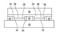
- P-contacts 44are formed on one or more remaining portions of p-type region 38 and n-contacts 42 are formed on one or more exposed portions of an n-type layer (n-type region 34 in FIG. 4 ).
- multiple n-contact regionsare interposed by p-contact regions.
- a single n-contact region and a single p-contact regionare formed.
- the p-contact 44 and n-contact 42are formed on the same side of the device.
- the contactsare generally reflective and the device is generally mounted such that light is extracted through the top surface of the device, n-type region 34 as shown in FIG. 4 .
- the deviceis mounted to a mount 40 through interconnects (not shown) between n- and p-contacts 42 and 44 and mount 40 .
- the interconnectsmay be gold-gold interconnects and the device may be attached to the mount by thermosonic bonding, or the interconnects may be solder and the device may be attached to the mount by reflow soldering.
- the growth substratemay be removed by a technique appropriate to the growth substrate, such as laser lift-off, etching, or a mechanical process such as grinding or chemical mechanical polishing.
- the semiconductor structureincludes a sacrificial semiconductor layer, which is implanted with an implant species such as H + that facilitates later separation of the semiconductor structure from the growth substrate.
- the semiconductor structureis separated from the growth substrate by activating the implanted species, for example by heating which causes the implanted area to expand and split the sacrificial layer.
- Implanting a sacrificial layer and separating a semiconductor structure from a growth substrate by activating the implant speciesis described in more detail in US Patent Application Publication 2005/0026394 and U.S. Pat. No. 5,374,564, which are incorporated herein by reference.
- the epitaxial substratemay be thinned, for example by photoelectrochemical etching.
- all or part of the epitaxial structure between substrate 20 and n-type region 34 illustrated in FIGS. 2 and 3is removed during thinning
- the top surface of the epitaxial structure remaining after thinningmay be textured to improve light extraction, for example by roughening or by patterning the surface with, for example, a lattice or photonic crystal structure.
- growth substrate 20 of FIGS. 2 and 3remains part of the device.
- a structure 46 known in the art, such as a wavelength converting element, a dichroic filter, or a lensmay be formed over the epitaxial structure. Light is extracted from the device through structure 46 .
- the device illustrated in FIG. 5light is extracted from the device through the top surface of the epitaxial structure, i.e. the surface on which the n- and p-contacts 42 and 44 are formed.
- the device layers 10are grown over a lattice mismatched layer 32 as described above.
- a rough p-type surfacemay be formed.
- the top portion of p-type region 38may be grown under conditions that form a rough surface
- a separate, rough p-type layer 48may be grown over p-type region 38
- a smooth surface of a p-type layermay be etched or roughened after growth, for example by photoelectrochemical etching.
- a layer of a transparent, conductive material 50 such as a transparent, conductive oxideis formed over the rough p-type surface.
- transparent conductive material 50may be indium tin oxide, zinc oxide, or ruthenium oxide.
- a portion of the p-type structure and light emitting region 36are removed to expose an n-type layer.
- N-contact 42is formed on the exposed n-type layer.
- P-contact 44is formed on a portion of the transparent, conductive material 50 .
- Material 50spreads current laterally through the p-type region 38 .
- N- and p-contacts 42 and 44may be limited in extent or made transparent.
- the devicemay be mounted such that light is extracted through the surface of transparent material 50 .
- FIG. 6illustrates a vertical injection LED.
- a p-contact 44is formed on the surface of p-type region 38 and the epitaxial structure is attached to a mount 52 through p-contact 44 . All or a portion of growth substrate 20 may be removed to expose the surface of an n-type region.
- An n-contact 42is formed on the surface exposed by removing the substrate, or on another exposed n-type surface, such as a side surface of an n-type region. As illustrated in FIG. 6 , n-contact 42 is formed on one side of the semiconductor structure, and a p-contact 44 is formed on the other side of the semiconductor structure. Electrical contact to the n-contact may be made with a wire bond 54 as illustrated in FIG. 6 or a metal bridge. The extent of the n-contact 42 may be limited as illustrated in FIG. 6 such that light may be extracted from the top of the device.
- a structureis included in the device to increase light extraction from the device, for example by increasing scattering.
- a surface of the epitaxial structuremay be roughened.
- scatteringis caused by a photonic crystal or lattice embedded in or formed on the surface of the III-nitride structure.
- changes in the optical index of refractionare provided in a periodic manner, at a spacing that is near the wavelength of light emitted by the light emitting region in the material.
- the parameters of the periodic index changesuch as the period and amplitude, may be selected to increase the amount of light extracted into a desired emission pattern.
- the size and spacing of a lattice or photonic crystalmay be selected to maximize the amount of light extracted in a direction normal to a top surface of the semiconductor structure. Selecting the parameters for and forming a photonic crystal are described in more detail in U.S. Pat. Nos. 7,642,108, 7,442,965, 7,442,964, 7,294,862, 7,279,718, 7,012,279, and 6,956,247, all of which are incorporated herein by reference.
- One or more wavelength converting materialsmay be disposed over the device to create white light or monochromatic light of other colors. Unconverted light emitted by the LED may be part of the final spectrum of light, though it need not be. Examples of common combinations include a blue-emitting LED combined with a yellow-emitting phosphor, a blue-emitting LED combined with green- and red-emitting phosphors, a UV-emitting LED combined with blue- and yellow-emitting phosphors, and a UV-emitting LED combined with blue-, green-, and red-emitting phosphors. Wavelength converting materials emitting other colors of light may be added to tailor the spectrum of light emitted from the device.
- wavelength converting materialsmay be mixed in a single wavelength converting layer or formed as discrete layers.
- suitable wavelength converting structuresinclude pre-formed ceramic phosphor layers that are glued or bonded to the LED, or a powder phosphor disposed in an organic encapsulant that is electrophoretically deposited, stenciled, screen printed, sprayed, sedimented, evaporated, sputtered, or otherwise dispensed over the LED.
Landscapes
- Engineering & Computer Science (AREA)
- Physics & Mathematics (AREA)
- Condensed Matter Physics & Semiconductors (AREA)
- General Physics & Mathematics (AREA)
- Manufacturing & Machinery (AREA)
- Computer Hardware Design (AREA)
- Microelectronics & Electronic Packaging (AREA)
- Power Engineering (AREA)
- Led Devices (AREA)
Abstract
Description
Claims (13)
Priority Applications (9)
| Application Number | Priority Date | Filing Date | Title |
|---|---|---|---|
| US12/783,197US8692261B2 (en) | 2010-05-19 | 2010-05-19 | Light emitting device grown on a relaxed layer |
| KR1020127033053AKR20130108512A (en) | 2010-05-19 | 2011-04-21 | Iii-nitride light-emitting device grown on a relaxed layer |
| CN201180024730.XACN102884643B (en) | 2010-05-19 | 2011-04-21 | The group III-nitride light-emitting device of growth on flabby sheaf |
| PCT/IB2011/051754WO2011148273A1 (en) | 2010-05-19 | 2011-04-21 | Iii-nitride light-emitting device grown on a relaxed layer |
| JP2013510695AJP2013526781A (en) | 2010-05-19 | 2011-04-21 | III-nitride light-emitting devices grown on relaxation layers |
| KR1020187002404AKR102147587B1 (en) | 2010-05-19 | 2011-04-21 | Ⅲ-nitride light-emitting device grown on a relaxed layer |
| EP11723656AEP2572386A1 (en) | 2010-05-19 | 2011-04-21 | Iii-nitride light-emitting device grown on a relaxed layer |
| TW100114332ATWI595683B (en) | 2010-05-19 | 2011-04-25 | Light emitting device and method of manufacturing same |
| US14/178,983US8945975B2 (en) | 2010-05-19 | 2014-02-12 | Light emitting device grown on a relaxed layer |
Applications Claiming Priority (1)
| Application Number | Priority Date | Filing Date | Title |
|---|---|---|---|
| US12/783,197US8692261B2 (en) | 2010-05-19 | 2010-05-19 | Light emitting device grown on a relaxed layer |
Related Child Applications (1)
| Application Number | Title | Priority Date | Filing Date |
|---|---|---|---|
| US14/178,983ContinuationUS8945975B2 (en) | 2010-05-19 | 2014-02-12 | Light emitting device grown on a relaxed layer |
Publications (2)
| Publication Number | Publication Date |
|---|---|
| US20110284890A1 US20110284890A1 (en) | 2011-11-24 |
| US8692261B2true US8692261B2 (en) | 2014-04-08 |
Family
ID=44318131
Family Applications (2)
| Application Number | Title | Priority Date | Filing Date |
|---|---|---|---|
| US12/783,197Active2031-02-08US8692261B2 (en) | 2010-05-19 | 2010-05-19 | Light emitting device grown on a relaxed layer |
| US14/178,983ActiveUS8945975B2 (en) | 2010-05-19 | 2014-02-12 | Light emitting device grown on a relaxed layer |
Family Applications After (1)
| Application Number | Title | Priority Date | Filing Date |
|---|---|---|---|
| US14/178,983ActiveUS8945975B2 (en) | 2010-05-19 | 2014-02-12 | Light emitting device grown on a relaxed layer |
Country Status (7)
| Country | Link |
|---|---|
| US (2) | US8692261B2 (en) |
| EP (1) | EP2572386A1 (en) |
| JP (1) | JP2013526781A (en) |
| KR (2) | KR20130108512A (en) |
| CN (1) | CN102884643B (en) |
| TW (1) | TWI595683B (en) |
| WO (1) | WO2011148273A1 (en) |
Families Citing this family (6)
| Publication number | Priority date | Publication date | Assignee | Title |
|---|---|---|---|---|
| JP5545269B2 (en)* | 2011-05-19 | 2014-07-09 | 豊田合成株式会社 | Group III nitride semiconductor light-emitting device and method for manufacturing the same |
| WO2013126458A1 (en)* | 2012-02-24 | 2013-08-29 | Skyworks Solutions, Inc. | Improved structures, devices and methods releated to copper interconnects for compound semiconductors |
| WO2014110195A1 (en)* | 2013-01-09 | 2014-07-17 | Sensor Electronic Technology, Inc. | Light emitting heterostructure with partially relaxed semiconductor layer |
| US9960315B2 (en) | 2013-01-09 | 2018-05-01 | Sensor Electronic Technology, Inc. | Light emitting heterostructure with partially relaxed semiconductor layer |
| KR102354184B1 (en) | 2018-03-06 | 2022-01-21 | 주식회사 엘지에너지솔루션 | Apparatus for aligning unit cell and method for manufacturing electrode assembly thereby |
| GB2586862B (en)* | 2019-09-06 | 2021-12-15 | Plessey Semiconductors Ltd | LED precursor incorporating strain relaxing structure |
Citations (15)
| Publication number | Priority date | Publication date | Assignee | Title |
|---|---|---|---|---|
| EP0977279A2 (en) | 1998-07-31 | 2000-02-02 | Xerox Corporation | AlGalnN LED and laser diode structures |
| US6495867B1 (en) | 2000-07-26 | 2002-12-17 | Axt, Inc. | InGaN/AlGaN/GaN multilayer buffer for growth of GaN on sapphire |
| US20040087055A1 (en)* | 2001-05-09 | 2004-05-06 | Nsc-Nanosemiconductor Gmbh | Semiconductor device and method of making same |
| US6956247B1 (en) | 2004-05-26 | 2005-10-18 | Lumileds Lighting U.S., Llc | Semiconductor light emitting device including photonic band gap material and luminescent material |
| US7012279B2 (en) | 2003-10-21 | 2006-03-14 | Lumileds Lighting U.S., Llc | Photonic crystal light emitting device |
| US20070096130A1 (en) | 2005-06-09 | 2007-05-03 | Philips Lumileds Lighting Company, Llc | LED Assembly Having Maximum Metal Support for Laser Lift-Off of Growth Substrate |
| WO2007096405A1 (en) | 2006-02-23 | 2007-08-30 | Azzurro Semiconductors Ag | Nitride semiconductor component and method for the production thereof |
| US7279718B2 (en) | 2002-01-28 | 2007-10-09 | Philips Lumileds Lighting Company, Llc | LED including photonic crystal structure |
| US20080149946A1 (en)* | 2006-12-22 | 2008-06-26 | Philips Lumileds Lighting Company, Llc | Semiconductor Light Emitting Device Configured To Emit Multiple Wavelengths Of Light |
| US20080149961A1 (en)* | 2006-12-22 | 2008-06-26 | Philips Lumileds Lighting Company, Llc | III-Nitride Light Emitting Devices Grown on Templates to Reduce Strain |
| US7442964B2 (en) | 2004-08-04 | 2008-10-28 | Philips Lumileds Lighting Company, Llc | Photonic crystal light emitting device with multiple lattices |
| US7442965B2 (en) | 2004-03-19 | 2008-10-28 | Philips Lumileds Lighting Company, Llc | Photonic crystal light emitting device |
| US20090267091A1 (en) | 2005-09-15 | 2009-10-29 | Yoshitaka Kinoshita | Semiconductor light emitting device |
| US20100072516A1 (en)* | 2008-09-25 | 2010-03-25 | Satoshi Tamura | Nitride semiconductor device |
| WO2010041657A1 (en) | 2008-10-07 | 2010-04-15 | 住友電気工業株式会社 | Gallium nitride semiconductor light-emitting element and method for producing the same, gallium nitride light-emitting diode, epitaxial wafer, and method for producing gallium nitride light-emitting diode |
Family Cites Families (4)
| Publication number | Priority date | Publication date | Assignee | Title |
|---|---|---|---|---|
| FR2681472B1 (en) | 1991-09-18 | 1993-10-29 | Commissariat Energie Atomique | PROCESS FOR PRODUCING THIN FILMS OF SEMICONDUCTOR MATERIAL. |
| FR2817394B1 (en) | 2000-11-27 | 2003-10-31 | Soitec Silicon On Insulator | METHOD FOR MANUFACTURING A SUBSTRATE, IN PARTICULAR FOR OPTICS, ELECTRONICS OR OPTOELECTRONICS AND SUBSTRATE OBTAINED THEREBY |
| CN100483666C (en)* | 2003-01-07 | 2009-04-29 | S.O.I.Tec绝缘体上硅技术公司 | Recycling of a wafer comprising a multi-layer structure after taking-off a thin layer |
| US7928448B2 (en)* | 2007-12-04 | 2011-04-19 | Philips Lumileds Lighting Company, Llc | III-nitride light emitting device including porous semiconductor layer |
- 2010
- 2010-05-19USUS12/783,197patent/US8692261B2/enactiveActive
- 2011
- 2011-04-21CNCN201180024730.XApatent/CN102884643B/enactiveActive
- 2011-04-21JPJP2013510695Apatent/JP2013526781A/ennot_activeWithdrawn
- 2011-04-21WOPCT/IB2011/051754patent/WO2011148273A1/enactiveApplication Filing
- 2011-04-21EPEP11723656Apatent/EP2572386A1/ennot_activeWithdrawn
- 2011-04-21KRKR1020127033053Apatent/KR20130108512A/ennot_activeCeased
- 2011-04-21KRKR1020187002404Apatent/KR102147587B1/enactiveActive
- 2011-04-25TWTW100114332Apatent/TWI595683B/enactive
- 2014
- 2014-02-12USUS14/178,983patent/US8945975B2/enactiveActive
Patent Citations (19)
| Publication number | Priority date | Publication date | Assignee | Title |
|---|---|---|---|---|
| EP0977279A2 (en) | 1998-07-31 | 2000-02-02 | Xerox Corporation | AlGalnN LED and laser diode structures |
| US6495867B1 (en) | 2000-07-26 | 2002-12-17 | Axt, Inc. | InGaN/AlGaN/GaN multilayer buffer for growth of GaN on sapphire |
| US20040087055A1 (en)* | 2001-05-09 | 2004-05-06 | Nsc-Nanosemiconductor Gmbh | Semiconductor device and method of making same |
| US7279718B2 (en) | 2002-01-28 | 2007-10-09 | Philips Lumileds Lighting Company, Llc | LED including photonic crystal structure |
| US7642108B2 (en) | 2002-01-28 | 2010-01-05 | Philips Lumileds Lighting Company, Llc | LED including photonic crystal structure |
| US7294862B2 (en) | 2003-10-21 | 2007-11-13 | Philips Lumileds Lighting Company, Llc | Photonic crystal light emitting device |
| US7012279B2 (en) | 2003-10-21 | 2006-03-14 | Lumileds Lighting U.S., Llc | Photonic crystal light emitting device |
| US7442965B2 (en) | 2004-03-19 | 2008-10-28 | Philips Lumileds Lighting Company, Llc | Photonic crystal light emitting device |
| US6956247B1 (en) | 2004-05-26 | 2005-10-18 | Lumileds Lighting U.S., Llc | Semiconductor light emitting device including photonic band gap material and luminescent material |
| US7442964B2 (en) | 2004-08-04 | 2008-10-28 | Philips Lumileds Lighting Company, Llc | Photonic crystal light emitting device with multiple lattices |
| US20070096130A1 (en) | 2005-06-09 | 2007-05-03 | Philips Lumileds Lighting Company, Llc | LED Assembly Having Maximum Metal Support for Laser Lift-Off of Growth Substrate |
| US20090267091A1 (en) | 2005-09-15 | 2009-10-29 | Yoshitaka Kinoshita | Semiconductor light emitting device |
| WO2007096405A1 (en) | 2006-02-23 | 2007-08-30 | Azzurro Semiconductors Ag | Nitride semiconductor component and method for the production thereof |
| US20080149946A1 (en)* | 2006-12-22 | 2008-06-26 | Philips Lumileds Lighting Company, Llc | Semiconductor Light Emitting Device Configured To Emit Multiple Wavelengths Of Light |
| US20080149961A1 (en)* | 2006-12-22 | 2008-06-26 | Philips Lumileds Lighting Company, Llc | III-Nitride Light Emitting Devices Grown on Templates to Reduce Strain |
| US7547908B2 (en) | 2006-12-22 | 2009-06-16 | Philips Lumilieds Lighting Co, Llc | III-nitride light emitting devices grown on templates to reduce strain |
| US20100072516A1 (en)* | 2008-09-25 | 2010-03-25 | Satoshi Tamura | Nitride semiconductor device |
| WO2010041657A1 (en) | 2008-10-07 | 2010-04-15 | 住友電気工業株式会社 | Gallium nitride semiconductor light-emitting element and method for producing the same, gallium nitride light-emitting diode, epitaxial wafer, and method for producing gallium nitride light-emitting diode |
| US20110182311A1 (en) | 2008-10-07 | 2011-07-28 | Sumitomo Electric Industries, Ltd. | Gallium nitride based semiconductor light-emitting device and method for fabricating the same, gallium nitride based light-emitting diode, epitaxial wafer, and method for fabricating gallium nitride light-emitting diode |
Non-Patent Citations (3)
| Title |
|---|
| A. Dadgar et al, Bright, Crack-Free InGaN/GaN Light Emitters on Si(111), Phys. Stat. Sol. (a) 192, No. 2, pp. 308-313, 2002. |
| Ke et al., Application of Nanosphere Lithography to LED Surface Texturing and to the Fabrication of Nanorod LED Arrays, IEEE Journal of Selected Topics in Quantum Electronics, vol. 15, No. 4, Jul./Aug. 2009, pp. 1242-1247.* |
| Lin et al., "High-efficiency InGaN-based light-emitting diodes with nanoporous GaN:Mg structure," Appl. Phys. Lett. 88, 083121 (2006).* |
Also Published As
| Publication number | Publication date |
|---|---|
| KR20180026474A (en) | 2018-03-12 |
| TW201201406A (en) | 2012-01-01 |
| US20110284890A1 (en) | 2011-11-24 |
| CN102884643A (en) | 2013-01-16 |
| US8945975B2 (en) | 2015-02-03 |
| KR20130108512A (en) | 2013-10-04 |
| TWI595683B (en) | 2017-08-11 |
| JP2013526781A (en) | 2013-06-24 |
| US20140162389A1 (en) | 2014-06-12 |
| CN102884643B (en) | 2016-04-13 |
| WO2011148273A1 (en) | 2011-12-01 |
| EP2572386A1 (en) | 2013-03-27 |
| KR102147587B1 (en) | 2020-08-25 |
Similar Documents
| Publication | Publication Date | Title |
|---|---|---|
| US8106403B2 (en) | III-nitride light emitting device incorporation boron | |
| US9991414B2 (en) | Method of forming a composite substrate | |
| US20090032828A1 (en) | III-Nitride Device Grown on Edge-Dislocation Template | |
| US8945975B2 (en) | Light emitting device grown on a relaxed layer | |
| US8536022B2 (en) | Method of growing composite substrate using a relaxed strained layer | |
| US9012250B2 (en) | Controlling pit formation in a III-nitride device |
Legal Events
| Date | Code | Title | Description |
|---|---|---|---|
| AS | Assignment | Owner name:PHILIPS LUMILEDS LIGHTING COMPANY, LLC, CALIFORNIA Free format text:ASSIGNMENT OF ASSIGNORS INTEREST;ASSIGNORS:KIM, ANDREW Y.;GRILLOT, PATRICK N.;REEL/FRAME:024409/0913 Effective date:20100517 Owner name:KONINKLIJKE PHILIPS ELECTRONICS N V, NETHERLANDS Free format text:ASSIGNMENT OF ASSIGNORS INTEREST;ASSIGNORS:KIM, ANDREW Y.;GRILLOT, PATRICK N.;REEL/FRAME:024409/0913 Effective date:20100517 | |
| STCF | Information on status: patent grant | Free format text:PATENTED CASE | |
| AS | Assignment | Owner name:KONINKLIJKE PHILIPS N.V., NETHERLANDS Free format text:CHANGE OF NAME;ASSIGNOR:KONINKLIJKE PHILIPS ELECTRONICS N.V.;REEL/FRAME:042810/0421 Effective date:20130515 | |
| AS | Assignment | Owner name:LUMILEDS LLC, CALIFORNIA Free format text:ASSIGNMENT OF ASSIGNORS INTEREST;ASSIGNOR:KONINKLIJKE PHILIPS N.V.;REEL/FRAME:042821/0001 Effective date:20170428 Owner name:LUMILEDS LLC, CALIFORNIA Free format text:CHANGE OF NAME;ASSIGNOR:PHILIPS LUMILEDS LIGHTING COMPANY, LLC;REEL/FRAME:042820/0900 Effective date:20150326 | |
| AS | Assignment | Owner name:DEUTSCHE BANK AG NEW YORK BRANCH, AS COLLATERAL AGENT, NEW YORK Free format text:SECURITY INTEREST;ASSIGNOR:LUMILEDS LLC;REEL/FRAME:043108/0001 Effective date:20170630 Owner name:DEUTSCHE BANK AG NEW YORK BRANCH, AS COLLATERAL AG Free format text:SECURITY INTEREST;ASSIGNOR:LUMILEDS LLC;REEL/FRAME:043108/0001 Effective date:20170630 | |
| MAFP | Maintenance fee payment | Free format text:PAYMENT OF MAINTENANCE FEE, 4TH YEAR, LARGE ENTITY (ORIGINAL EVENT CODE: M1551) Year of fee payment:4 | |
| MAFP | Maintenance fee payment | Free format text:PAYMENT OF MAINTENANCE FEE, 8TH YEAR, LARGE ENTITY (ORIGINAL EVENT CODE: M1552); ENTITY STATUS OF PATENT OWNER: LARGE ENTITY Year of fee payment:8 | |
| AS | Assignment | Owner name:SOUND POINT AGENCY LLC, NEW YORK Free format text:SECURITY INTEREST;ASSIGNORS:LUMILEDS LLC;LUMILEDS HOLDING B.V.;REEL/FRAME:062299/0338 Effective date:20221230 | |
| AS | Assignment | Owner name:LUMILEDS HOLDING B.V., NETHERLANDS Free format text:RELEASE BY SECURED PARTY;ASSIGNOR:SOUND POINT AGENCY LLC;REEL/FRAME:070046/0001 Effective date:20240731 Owner name:LUMILEDS LLC, CALIFORNIA Free format text:RELEASE BY SECURED PARTY;ASSIGNOR:SOUND POINT AGENCY LLC;REEL/FRAME:070046/0001 Effective date:20240731 | |
| AS | Assignment | Owner name:LUMILEDS SINGAPORE PTE. LTD., SINGAPORE Free format text:ASSIGNMENT OF ASSIGNORS INTEREST;ASSIGNOR:LUMILEDS LLC;REEL/FRAME:071888/0086 Effective date:20250708 | |
| MAFP | Maintenance fee payment | Free format text:PAYMENT OF MAINTENANCE FEE, 12TH YEAR, LARGE ENTITY (ORIGINAL EVENT CODE: M1553); ENTITY STATUS OF PATENT OWNER: LARGE ENTITY Year of fee payment:12 |