US8687385B2 - Low power converter - Google Patents
Low power converterDownload PDFInfo
- Publication number
- US8687385B2 US8687385B2US12/954,635US95463510AUS8687385B2US 8687385 B2US8687385 B2US 8687385B2US 95463510 AUS95463510 AUS 95463510AUS 8687385 B2US8687385 B2US 8687385B2
- Authority
- US
- United States
- Prior art keywords
- output
- signal
- power
- conversion circuit
- operably coupled
- Prior art date
- Legal status (The legal status is an assumption and is not a legal conclusion. Google has not performed a legal analysis and makes no representation as to the accuracy of the status listed.)
- Active, expires
Links
- 238000006243chemical reactionMethods0.000claimsabstractdescription46
- 239000003990capacitorSubstances0.000claimsdescription14
- 238000004146energy storageMethods0.000claimsdescription6
- 238000012544monitoring processMethods0.000claimsdescription6
- 230000004044responseEffects0.000claimsdescription6
- 238000004891communicationMethods0.000claimsdescription5
- 230000005291magnetic effectEffects0.000claimsdescription3
- 230000003287optical effectEffects0.000claimsdescription2
- 238000003384imaging methodMethods0.000claims1
- 230000008901benefitEffects0.000description5
- 238000000034methodMethods0.000description3
- 230000005540biological transmissionEffects0.000description2
- 238000007792additionMethods0.000description1
- 230000003466anti-cipated effectEffects0.000description1
- 238000003491arrayMethods0.000description1
- 230000008878couplingEffects0.000description1
- 238000010168coupling processMethods0.000description1
- 238000005859coupling reactionMethods0.000description1
- 230000003247decreasing effectEffects0.000description1
- 238000013461designMethods0.000description1
- 238000001514detection methodMethods0.000description1
- 238000010586diagramMethods0.000description1
- 238000004134energy conservationMethods0.000description1
- 230000001939inductive effectEffects0.000description1
- 238000003780insertionMethods0.000description1
- 230000037431insertionEffects0.000description1
- 239000000463materialSubstances0.000description1
- 238000012986modificationMethods0.000description1
- 230000004048modificationEffects0.000description1
- 230000000737periodic effectEffects0.000description1
- 230000009467reductionEffects0.000description1
Images


Classifications
- H—ELECTRICITY
- H02—GENERATION; CONVERSION OR DISTRIBUTION OF ELECTRIC POWER
- H02M—APPARATUS FOR CONVERSION BETWEEN AC AND AC, BETWEEN AC AND DC, OR BETWEEN DC AND DC, AND FOR USE WITH MAINS OR SIMILAR POWER SUPPLY SYSTEMS; CONVERSION OF DC OR AC INPUT POWER INTO SURGE OUTPUT POWER; CONTROL OR REGULATION THEREOF
- H02M3/00—Conversion of DC power input into DC power output
- H02M3/22—Conversion of DC power input into DC power output with intermediate conversion into AC
- H02M3/24—Conversion of DC power input into DC power output with intermediate conversion into AC by static converters
- H02M3/28—Conversion of DC power input into DC power output with intermediate conversion into AC by static converters using discharge tubes with control electrode or semiconductor devices with control electrode to produce the intermediate AC
- H02M3/325—Conversion of DC power input into DC power output with intermediate conversion into AC by static converters using discharge tubes with control electrode or semiconductor devices with control electrode to produce the intermediate AC using devices of a triode or a transistor type requiring continuous application of a control signal
- H02M3/335—Conversion of DC power input into DC power output with intermediate conversion into AC by static converters using discharge tubes with control electrode or semiconductor devices with control electrode to produce the intermediate AC using devices of a triode or a transistor type requiring continuous application of a control signal using semiconductor devices only
- H02M3/33507—Conversion of DC power input into DC power output with intermediate conversion into AC by static converters using discharge tubes with control electrode or semiconductor devices with control electrode to produce the intermediate AC using devices of a triode or a transistor type requiring continuous application of a control signal using semiconductor devices only with automatic control of the output voltage or current, e.g. flyback converters
- H—ELECTRICITY
- H02—GENERATION; CONVERSION OR DISTRIBUTION OF ELECTRIC POWER
- H02M—APPARATUS FOR CONVERSION BETWEEN AC AND AC, BETWEEN AC AND DC, OR BETWEEN DC AND DC, AND FOR USE WITH MAINS OR SIMILAR POWER SUPPLY SYSTEMS; CONVERSION OF DC OR AC INPUT POWER INTO SURGE OUTPUT POWER; CONTROL OR REGULATION THEREOF
- H02M1/00—Details of apparatus for conversion
- H02M1/0003—Details of control, feedback or regulation circuits
- H02M1/0032—Control circuits allowing low power mode operation, e.g. in standby mode
- Y—GENERAL TAGGING OF NEW TECHNOLOGICAL DEVELOPMENTS; GENERAL TAGGING OF CROSS-SECTIONAL TECHNOLOGIES SPANNING OVER SEVERAL SECTIONS OF THE IPC; TECHNICAL SUBJECTS COVERED BY FORMER USPC CROSS-REFERENCE ART COLLECTIONS [XRACs] AND DIGESTS
- Y02—TECHNOLOGIES OR APPLICATIONS FOR MITIGATION OR ADAPTATION AGAINST CLIMATE CHANGE
- Y02B—CLIMATE CHANGE MITIGATION TECHNOLOGIES RELATED TO BUILDINGS, e.g. HOUSING, HOUSE APPLIANCES OR RELATED END-USER APPLICATIONS
- Y02B70/00—Technologies for an efficient end-user side electric power management and consumption
- Y02B70/10—Technologies improving the efficiency by using switched-mode power supplies [SMPS], i.e. efficient power electronics conversion e.g. power factor correction or reduction of losses in power supplies or efficient standby modes
Definitions
- the inventionrelates to the more efficient utilization of energy resources and energy conservation. More particularly, the invention relates to electronic systems for conversion of an alternating current (AC) to a direct current (DC), and to the use of low power converters to power DC devices and/or charge DC energy storage apparatus.
- ACalternating current
- DCdirect current
- the inventionprovides advances in the arts with novel methods and apparatus directed to providing AC/DC converters, adapters, and charging systems with capabilities for detecting load conditions and halting the AC to DC conversion when the load does not require it.
- the systementers into an extremely low power standby mode until output power is needed at the load, and/or until a standby mode power supply residing with the converter is replenished for another low power standby operation cycle.
- an AC/DC converter systemis configured for receiving an AC power input signal and converting the input signal to a DC output signal.
- An enabling circuitis provided for sensing an output parameter and for switching the conversion circuit between an active state and an inactive state in response to the sensed output parameter.
- the system described immediately abovealso includes a power storage device in the enabling circuit for supplying power thereto.
- preferred embodiments of the system of the inventioninclude systems wherein the DC output is operably coupled with portable electronic apparatus.
- a preferred embodiment of an AC to DC converter systemhas an input for receiving an AC input and a conversion circuit for converting the AC input signal to a DC output signal.
- An enabling circuitis adapted to switch the conversion circuit between an active state and an inactive state in response to a load switch.
- an AC to DC converter systemhas an AC power input, a conversion circuit for converting the AC signal to a DC output signal.
- An enabling circuitconfigured to switch the conversion circuit between an active state and an inactive state in response to a sensed parameter or a load switch, is capacitively coupled for receiving power from the AC input.
- the inventionhas advantages including but not limited to one or more of the following; providing efficient AC to DC power conversion at a range of operating levels and/or providing an extremely low power standby mode adaptable to real time load conditions.
- FIG. 1is a simplified schematic drawing of an example of a preferred embodiment of a circuit for sensing real time power requirements for use in AC/DC power conversion systems according to the invention
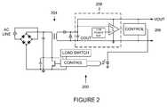
- FIG. 2is a simplified schematic drawing showing an example of another preferred embodiment of low power converter circuitry according to the principles of the invention
- FIG. 3is a simplified schematic drawing illustrating another example of an alternative preferred embodiment of low power converter circuitry according to the invention.
- FIG. 4is a simplified schematic drawing of an example of an alternative preferred embodiment of low power converter circuitry according to the invention.
- FIG. 5is a simplified schematic drawing of an example of a preferred embodiment of a preferred embodiment of low power converter circuitry according to the invention.
- the inventionprovides circuits and systems by which AC to DC adapters and/or chargers may be enabled during periods when a DC load is detected, and by which they may be placed in a low power standby state during periods when it is detected that AC/DC conversion is not required.
- the low power circuits and systems in presently preferred embodimentsalso include capabilities for ensuring that the system has access to sufficient power to operate in standby mode for significant periods of time, preferably including the capability for replenishing energy stored for use in standby mode. Referring primarily to FIG.
- an AC to DC converter circuit 100has an input 102 configured for receiving an AC power input signal and a power conversion circuit 104 , typically including transformers and rectifiers as known in the art, for converting the AC input signal to a DC output signal appropriate for delivery to a DC load at an output node 106 .
- the DC load(s) connected to the output 106may constitute one or more DC-operated circuits and/or battery and/or other DC power storage devices or arrays of such devices.
- an enabling circuit 108Deployed between the power conversion circuit 104 and the output 106 , an enabling circuit 108 is configured to sense one or more output parameter associated with the output 106 , and is further configured for switching the power conversion circuit 104 between an active state and an inactive standby state in response to the sensed output parameter.
- the enabling circuit 108includes a low power, preferably on the order of nano-amps (nA), comparator 110 for sensing the DC output voltage (V OUT ) at the output node 106 .
- a low powerpreferably on the order of nano-amps (nA)
- comparator 110for sensing the DC output voltage (V OUT ) at the output node 106 .
- the enabling circuit 108 comparator 110may alternatively be configured to sense other output parameters such as, for example, current, power, impedance, capacitance, magnetic field(s), or to receive an external signal such as a wireless transmission or timing signal.
- An alternative implementation, for example,may include a comparator configured for monitoring output current instead of output voltage.
- the power conversion circuit 104If sufficient output voltage is available and the output current is below a certain predetermined threshold, then the power conversion circuit 104 is not needed for supplying output current, and is placed in its standby state. When the output voltage drops below a certain predetermined threshold, or when the output current exceeds a certain threshold, the conversion circuitry 104 is again operated in the active state to supply the output current. It is believed that for many applications, monitoring output current without monitoring the output voltage will be sufficient for control of the system 100 .
- the enabling circuit 108is preferably operated using power from an energy storage device provided for that purpose, such as a battery or capacitor, e.g., C OUT in FIG. 1 .
- the comparator 110may be operated using output from the conversion circuitry 104 , and/or from the dedicated storage device, e.g., capacitor C OUT .
- the power conversion circuit 104is activated for converting an AC signal received at the input 102 into a DC signal at the output terminal 106 connected to the detected load (not shown).
- the comparator 110is configured to detect, based on one or more selected parameter(s) reaching selected threshold(s), whether operation of the power conversion circuitry 104 in either an active state or inactive standby state is required.
- the power conversion circuit 104is placed in an inactive standby state. While the power conversion circuit 104 is in the standby state, the comparator 110 is powered by power stored in the enabling circuit 108 , in this example a charge stored on the capacitor C OUT . Since the comparator 110 is preferably configured to operate with extremely low quiescent current, a relatively small sized capacitor C OUT provides significant operating time.
- the power conversion circuitry 104When the voltage on the capacitor C OUT drops below a predetermined threshold level, the power conversion circuitry 104 is activated. During the operation of the power conversion circuit 104 in this active state, the charge on the capacitor C OUT is replenished. When the sensed output parameter, in this example voltage (V OUT ), reaches a predetermined threshold the power conversion circuitry 104 turns off, entering the inactive state, and only the low-power comparator 110 remains on, minimizing the system 100 power consumption.
- V OUTvoltage
- the parameter monitored for making the determination of when to switch the conversion circuitry 204 to or from the active or standby modemay be a signal communicated by a load connected to the output 206 .
- the system 200as illustrated in FIG. 2 , may be configured such that a load connected at the output 206 communicates to the AC/DC converter 204 using a periodic, watchdog type protocol, wireless signal, or other serial/parallel communication.
- the enabling circuit 208receives a signal from the load communicating that power is required to be supplied at the output 206 . Accordingly, the enabling circuit 208 causes the conversion circuit 204 to operate in the active mode.
- the enabling circuit 208When a signal is received indicating that power is not required at the output 206 , the enabling circuit 208 causes the conversion circuit 204 to enter the standby mode and stop consuming and supplying power. The enabling circuit 108 then continues to monitor the output 206 for a signal which would again cause it to place the converter circuit 204 in the active state.
- FIG. 3an alternative implementation of the invention is shown.
- the presence of a load at the output 306is detected by the operation of a switch 302 , preferably located in the adapter plug in typical power converter applications.
- the converter circuit 304is enabled by operation of the enabling circuit 308 .
- the power conversion circuitry 304is placed in its inactive standby state and the enabling circuit 308 is placed in low power mode, drawing its power from an associated power storage device, in this example capacitor C CONTROL .
- the load switch 302can be implemented in a variety of ways as long as communication with the enabling circuit is provided.
- a mechanical switchis used.
- the switchis activated by the completion and/or removal of a physical connection to the output node 306 , e.g., by insertion or removal of a suitable output jack 306 into compatible apparatus.
- a proximity switchsuch as a capacitive, inductive, optical, magnetic, resistive, or infrared sensor activated switch may be used without departure from the invention.
- Additional embodiments of the low power converter of the inventionfurther address the challenge of guaranteeing system startup when the converter system has been idle for an extended period of time.
- the power storage element of the enabling circuite.g., the output capacitor C OUT of FIG. 1
- FIG. 4An alternative embodiment of low power converter circuitry is shown in FIG. 4 .
- a timer 402is coupled to the primary side 404 of the power conversion circuit 404 .
- the system 400may be configured to automatically turn on periodically and convert power in its active state for a brief period of time.
- the output capacitor Cmay be recharged from time to time, ensuring that the system 400 retains sufficient power to continue monitoring the output 406 for detection of demand for DC output requiring the operation of the power conversion circuit 404 in its active mode. It is contemplated that the timer-induced “on” period can be relatively brief, thus the overall amount of power consumed by the forced turn-on remains small.
- additional external signalsmay be used such as wired or wireless communications signals suitable for causing the conversion circuitry 404 to recharge the enabling circuit 408 power source, e.g., storage capacitor C, as shown, or other suitable storage device.
- an alternative embodiment of the low power converter 500has been developed in which capacitive coupling may be used to provide startup power for the enabling circuit 508 .
- the AC signal on the primary side of the conversion circuit 504operates to pump charge across the capacitor C PUMP , providing a start-up voltage for the enabling circuit 508 connected with the secondary side 510 of the conversion circuit 504 .
- a Zener diode Z CLAMP coupled between the enabling circuit 508 and groundis preferably used to limit the voltage sufficiently to protect the circuit 500 from over voltage.
- the size of the capacitor C PUMPmay be selected to limit the power transmission to the secondary side 510 of the conversion circuit 504 , and thus also limit the total power dissipated by the enabling circuit 508 in this configuration.
- the methods and apparatus of the inventionprovide one or more advantages including but not limited to improved efficiency in power supply, AC/DC conversion, and energy storage apparatus charging systems. While the invention has been described with reference to certain illustrative embodiments, those described herein are not intended to be construed in a limiting sense. For example, variations or combinations of steps or materials in the embodiments shown and described may be used in particular cases without departure from the invention. Modifications and combinations of the illustrative embodiments as well as other advantages and embodiments of the invention will be apparent to persons skilled in the arts upon reference to the drawings, description, and claims.
Landscapes
- Engineering & Computer Science (AREA)
- Power Engineering (AREA)
- Charge And Discharge Circuits For Batteries Or The Like (AREA)
- Dc-Dc Converters (AREA)
Abstract
Description
Claims (19)
Priority Applications (5)
| Application Number | Priority Date | Filing Date | Title |
|---|---|---|---|
| US12/954,635US8687385B2 (en) | 2009-11-25 | 2010-11-25 | Low power converter |
| US14/230,645US9214867B2 (en) | 2009-11-25 | 2014-03-31 | Low power converter |
| US14/970,396US9793814B2 (en) | 2009-11-25 | 2015-12-15 | Low power converter |
| US15/729,498US10574297B2 (en) | 2009-11-25 | 2017-10-10 | Multi-use wireless power and data system |
| US16/799,239US11368191B2 (en) | 2009-11-25 | 2020-02-24 | Multi-use wireless power and data system |
Applications Claiming Priority (2)
| Application Number | Priority Date | Filing Date | Title |
|---|---|---|---|
| US26464409P | 2009-11-25 | 2009-11-25 | |
| US12/954,635US8687385B2 (en) | 2009-11-25 | 2010-11-25 | Low power converter |
Related Parent Applications (1)
| Application Number | Title | Priority Date | Filing Date |
|---|---|---|---|
| US14/982,952Continuation-In-PartUS9843314B2 (en) | 2009-11-25 | 2015-12-29 | Pop and click noise reduction |
Related Child Applications (1)
| Application Number | Title | Priority Date | Filing Date |
|---|---|---|---|
| US14/230,645DivisionUS9214867B2 (en) | 2009-11-25 | 2014-03-31 | Low power converter |
Publications (2)
| Publication Number | Publication Date |
|---|---|
| US20110122666A1 US20110122666A1 (en) | 2011-05-26 |
| US8687385B2true US8687385B2 (en) | 2014-04-01 |
Family
ID=44061974
Family Applications (3)
| Application Number | Title | Priority Date | Filing Date |
|---|---|---|---|
| US12/954,635Active2032-05-10US8687385B2 (en) | 2009-11-25 | 2010-11-25 | Low power converter |
| US14/230,645Expired - Fee RelatedUS9214867B2 (en) | 2009-11-25 | 2014-03-31 | Low power converter |
| US14/970,396Expired - Fee RelatedUS9793814B2 (en) | 2009-11-25 | 2015-12-15 | Low power converter |
Family Applications After (2)
| Application Number | Title | Priority Date | Filing Date |
|---|---|---|---|
| US14/230,645Expired - Fee RelatedUS9214867B2 (en) | 2009-11-25 | 2014-03-31 | Low power converter |
| US14/970,396Expired - Fee RelatedUS9793814B2 (en) | 2009-11-25 | 2015-12-15 | Low power converter |
Country Status (1)
| Country | Link |
|---|---|
| US (3) | US8687385B2 (en) |
Cited By (13)
| Publication number | Priority date | Publication date | Assignee | Title |
|---|---|---|---|---|
| US9599660B2 (en) | 2009-02-23 | 2017-03-21 | Triune Ip, Llc | Electrical interconnect status monitoring system |
| US9843314B2 (en) | 2011-07-10 | 2017-12-12 | Triune Systems, LLC | Pop and click noise reduction |
| US9853441B2 (en) | 2011-07-10 | 2017-12-26 | Triune Systems, LLC | Voltage transient protection circuitry |
| US10079090B2 (en) | 2010-12-01 | 2018-09-18 | Triune Systems, LLC | Multiple coil data transmission system |
| US10186897B2 (en) | 2012-02-21 | 2019-01-22 | Triune Ip Llc | Scalable harvesting system and method |
| US10250081B2 (en) | 2012-01-17 | 2019-04-02 | Triune Systems, LLC | Method and system of wireless power transfer foreign object detection |
| USRE47441E1 (en) | 2008-07-21 | 2019-06-18 | Triune Ip Llc | Monitoring method, circuit and system |
| US10348131B2 (en) | 2010-12-01 | 2019-07-09 | Triune Systems, LLC | Couple inductor power transfer system |
| US10396590B2 (en) | 2011-03-22 | 2019-08-27 | Triune Systems, LLC | Variable power energy harvesting system |
| US10574297B2 (en) | 2009-11-25 | 2020-02-25 | Triune Ip, Llc | Multi-use wireless power and data system |
| USRE47900E1 (en) | 2008-07-21 | 2020-03-10 | Triune Ip, Llc | Memory for programming a floating gate using an analog comparison device coupled to a tunneling device |
| US10673489B2 (en) | 2014-03-04 | 2020-06-02 | Triune Ip Llc | Isolation for communication and power |
| US10854378B2 (en) | 2009-02-23 | 2020-12-01 | Triune Ip Llc | Wireless power transmittal |
Families Citing this family (5)
| Publication number | Priority date | Publication date | Assignee | Title |
|---|---|---|---|---|
| US20150026499A1 (en)* | 2013-07-18 | 2015-01-22 | Chih-Ju HUANG | Circuit for changing load operation using temporary power-off means |
| US9685852B2 (en)* | 2015-07-02 | 2017-06-20 | Dynapower Company Llc | Power converter system having active standby mode and method of controlling the same |
| US11381281B2 (en) | 2020-02-04 | 2022-07-05 | Powermat Technologies Ltd. | Fast data transmission for wireless power transfer systems |
| CN112994461A (en)* | 2021-03-26 | 2021-06-18 | 浙江高泰昊能科技有限公司 | DC-DC isolation power supply circuit and working method thereof |
| CN114844367B (en)* | 2022-05-30 | 2024-08-30 | 苏州美思迪赛半导体技术有限公司 | Centralized control system and method for power output adjustment |
Citations (3)
| Publication number | Priority date | Publication date | Assignee | Title |
|---|---|---|---|---|
| US5818707A (en)* | 1995-11-16 | 1998-10-06 | Samsung Electronic, Co., Ltd. | Simplified active power factor correction controller IC |
| US6295217B1 (en)* | 1999-03-26 | 2001-09-25 | Sarnoff Corporation | Low power dissipation power supply and controller |
| US20110305051A1 (en)* | 2010-06-11 | 2011-12-15 | System General Corp. | Start-up circuit with low standby power loss for power converters |
Family Cites Families (7)
| Publication number | Priority date | Publication date | Assignee | Title |
|---|---|---|---|---|
| US6462437B1 (en)* | 1999-11-12 | 2002-10-08 | Koninklijke Philips Electronics N.V. | System and method for alternating standby mode |
| KR100840246B1 (en)* | 2002-01-25 | 2008-06-20 | 페어차일드코리아반도체 주식회사 | Flyback converter |
| DE10228742A1 (en)* | 2002-06-27 | 2004-01-15 | Patent-Treuhand-Gesellschaft für elektrische Glühlampen mbH | Supply circuit, in particular for discharge lamps |
| TWI328149B (en)* | 2006-01-09 | 2010-08-01 | System General Corp | A power converter for activating a pfc circuit with feed-forward voltage compensation |
| JP4775441B2 (en)* | 2006-06-30 | 2011-09-21 | パナソニック電工株式会社 | Switching power supply |
| US7535734B2 (en)* | 2006-10-19 | 2009-05-19 | Heng-Yi Li | High power-factor AC/DC converter with parallel power processing |
| US9164133B2 (en)* | 2012-11-02 | 2015-10-20 | Power Integrations, Inc. | Switched averaging error amplifier |
- 2010
- 2010-11-25USUS12/954,635patent/US8687385B2/enactiveActive
- 2014
- 2014-03-31USUS14/230,645patent/US9214867B2/ennot_activeExpired - Fee Related
- 2015
- 2015-12-15USUS14/970,396patent/US9793814B2/ennot_activeExpired - Fee Related
Patent Citations (3)
| Publication number | Priority date | Publication date | Assignee | Title |
|---|---|---|---|---|
| US5818707A (en)* | 1995-11-16 | 1998-10-06 | Samsung Electronic, Co., Ltd. | Simplified active power factor correction controller IC |
| US6295217B1 (en)* | 1999-03-26 | 2001-09-25 | Sarnoff Corporation | Low power dissipation power supply and controller |
| US20110305051A1 (en)* | 2010-06-11 | 2011-12-15 | System General Corp. | Start-up circuit with low standby power loss for power converters |
Cited By (16)
| Publication number | Priority date | Publication date | Assignee | Title |
|---|---|---|---|---|
| USRE47900E1 (en) | 2008-07-21 | 2020-03-10 | Triune Ip, Llc | Memory for programming a floating gate using an analog comparison device coupled to a tunneling device |
| USRE47441E1 (en) | 2008-07-21 | 2019-06-18 | Triune Ip Llc | Monitoring method, circuit and system |
| US11309126B2 (en) | 2009-02-23 | 2022-04-19 | Triune Systems, LLC | Wireless power transmittal |
| US10854378B2 (en) | 2009-02-23 | 2020-12-01 | Triune Ip Llc | Wireless power transmittal |
| US9599660B2 (en) | 2009-02-23 | 2017-03-21 | Triune Ip, Llc | Electrical interconnect status monitoring system |
| US11368191B2 (en) | 2009-11-25 | 2022-06-21 | Triune Ip, Llc | Multi-use wireless power and data system |
| US10574297B2 (en) | 2009-11-25 | 2020-02-25 | Triune Ip, Llc | Multi-use wireless power and data system |
| US10079090B2 (en) | 2010-12-01 | 2018-09-18 | Triune Systems, LLC | Multiple coil data transmission system |
| US11159053B2 (en) | 2010-12-01 | 2021-10-26 | Triune Systems, LLC | Coupled inductor power transfer system |
| US10348131B2 (en) | 2010-12-01 | 2019-07-09 | Triune Systems, LLC | Couple inductor power transfer system |
| US10396590B2 (en) | 2011-03-22 | 2019-08-27 | Triune Systems, LLC | Variable power energy harvesting system |
| US9853441B2 (en) | 2011-07-10 | 2017-12-26 | Triune Systems, LLC | Voltage transient protection circuitry |
| US9843314B2 (en) | 2011-07-10 | 2017-12-12 | Triune Systems, LLC | Pop and click noise reduction |
| US10250081B2 (en) | 2012-01-17 | 2019-04-02 | Triune Systems, LLC | Method and system of wireless power transfer foreign object detection |
| US10186897B2 (en) | 2012-02-21 | 2019-01-22 | Triune Ip Llc | Scalable harvesting system and method |
| US10673489B2 (en) | 2014-03-04 | 2020-06-02 | Triune Ip Llc | Isolation for communication and power |
Also Published As
| Publication number | Publication date |
|---|---|
| US20160105115A1 (en) | 2016-04-14 |
| US20110122666A1 (en) | 2011-05-26 |
| US9214867B2 (en) | 2015-12-15 |
| US20140211514A1 (en) | 2014-07-31 |
| US9793814B2 (en) | 2017-10-17 |
Similar Documents
| Publication | Publication Date | Title |
|---|---|---|
| US8687385B2 (en) | Low power converter | |
| US9559596B2 (en) | Ultra-low power converter | |
| US7923869B2 (en) | Power adapter | |
| KR101445011B1 (en) | Power converter with reduced power consumption when toggling between sleep and normal modes during device charging | |
| CN201570873U (en) | Device and integrated circuit for achieving intelligent power management of USB port | |
| US7911817B2 (en) | Systems and methods for controlling energy consumption of AC-DC adapters | |
| US9019726B2 (en) | Power converters with quasi-zero power consumption | |
| TWI513168B (en) | Power conversion apparatus | |
| US9577632B2 (en) | Wireless switching circuit | |
| JP2007143397A (en) | Power supply control method, current / voltage conversion circuit, and electronic device | |
| JP4489748B2 (en) | Power supply device and power supply method for electronic device | |
| US20090287947A1 (en) | Circuit and method for ultra-low idle power | |
| CN105075064A (en) | Wireless power transmitting unit, wireless power receiving unit, and control method | |
| TWI633426B (en) | Power supply system and method | |
| KR20110050436A (en) | Load state control power circuit | |
| CN104953682A (en) | Circuit with wireless charging transmitting function and wireless charging receiving function and device thereof | |
| CN103516038A (en) | Power-saving circuit and electronic device | |
| CN218569860U (en) | Wireless charging device | |
| JP2003333747A (en) | Power source device for electronic apparatus and method for controlling the same | |
| US20110187195A1 (en) | Intelligent Low-Consumption Adaptor | |
| CN107515658A (en) | Power supply system and power supply method | |
| KR101266505B1 (en) | Charging device for standby power reduction | |
| Tsai et al. | Using an ultrasound module to reduce the standby power consumption of a PC monitor | |
| MXPA01011485A (en) | Telephone-line based power supply system. | |
| JP2005218149A (en) | Power relay device |
Legal Events
| Date | Code | Title | Description |
|---|---|---|---|
| AS | Assignment | Owner name:TRIUNE IP LLC, TEXAS Free format text:ASSIGNMENT OF ASSIGNORS INTEREST;ASSIGNORS:TEGGATZ, ROSS;SMITH, BRETT;ATRASH, AMER;AND OTHERS;SIGNING DATES FROM 20101115 TO 20101117;REEL/FRAME:025423/0244 | |
| STCF | Information on status: patent grant | Free format text:PATENTED CASE | |
| AS | Assignment | Owner name:HSBC BANK USA, NATIONAL ASSOCIATION, CALIFORNIA Free format text:SECURITY INTEREST;ASSIGNOR:TRIUNE IP, LLC;REEL/FRAME:035732/0326 Effective date:20150513 | |
| FEPP | Fee payment procedure | Free format text:PAT HOLDER NO LONGER CLAIMS SMALL ENTITY STATUS, ENTITY STATUS SET TO UNDISCOUNTED (ORIGINAL EVENT CODE: STOL); ENTITY STATUS OF PATENT OWNER: LARGE ENTITY | |
| AS | Assignment | Owner name:HSBC BANK USA, NATIONAL ASSOCIATION, AS ADMINISTRATIVE AGENT, CALIFORNIA Free format text:SECURITY INTEREST;ASSIGNORS:SEMTECH CORPORATION;SEMTECH NEW YORK CORPORATION;SIERRA MONOLITHICS, INC.;AND OTHERS;SIGNING DATES FROM 20151115 TO 20161115;REEL/FRAME:040646/0799 Owner name:HSBC BANK USA, NATIONAL ASSOCIATION, AS ADMINISTRA Free format text:SECURITY INTEREST;ASSIGNORS:SEMTECH CORPORATION;SEMTECH NEW YORK CORPORATION;SIERRA MONOLITHICS, INC.;AND OTHERS;SIGNING DATES FROM 20151115 TO 20161115;REEL/FRAME:040646/0799 | |
| MAFP | Maintenance fee payment | Free format text:PAYMENT OF MAINTENANCE FEE, 4TH YEAR, LARGE ENTITY (ORIGINAL EVENT CODE: M1551) Year of fee payment:4 | |
| MAFP | Maintenance fee payment | Free format text:PAYMENT OF MAINTENANCE FEE, 8TH YEAR, LARGE ENTITY (ORIGINAL EVENT CODE: M1552); ENTITY STATUS OF PATENT OWNER: LARGE ENTITY Year of fee payment:8 | |
| AS | Assignment | Owner name:JPMORGAN CHASE BANK, N.A., AS SUCCESSOR AGENT, ILLINOIS Free format text:ASSIGNMENT OF PATENT SECURITY INTEREST PREVIOUSLY RECORDED AT REEL/FRAME (040646/0799);ASSIGNOR:HSBC BANK USA, NATIONAL ASSOCIATION, AS RESIGNING AGENT;REEL/FRAME:062781/0544 Effective date:20230210 |