US8685630B2 - Methods of forming a pattern in a material and methods of forming openings in a material to be patterned - Google Patents
Methods of forming a pattern in a material and methods of forming openings in a material to be patternedDownload PDFInfo
- Publication number
- US8685630B2 US8685630B2US13/963,096US201313963096AUS8685630B2US 8685630 B2US8685630 B2US 8685630B2US 201313963096 AUS201313963096 AUS 201313963096AUS 8685630 B2US8685630 B2US 8685630B2
- Authority
- US
- United States
- Prior art keywords
- portions
- apertures
- photoresist
- mask
- openings
- Prior art date
- Legal status (The legal status is an assumption and is not a legal conclusion. Google has not performed a legal analysis and makes no representation as to the accuracy of the status listed.)
- Active
Links
Images


Classifications
- G—PHYSICS
- G03—PHOTOGRAPHY; CINEMATOGRAPHY; ANALOGOUS TECHNIQUES USING WAVES OTHER THAN OPTICAL WAVES; ELECTROGRAPHY; HOLOGRAPHY
- G03F—PHOTOMECHANICAL PRODUCTION OF TEXTURED OR PATTERNED SURFACES, e.g. FOR PRINTING, FOR PROCESSING OF SEMICONDUCTOR DEVICES; MATERIALS THEREFOR; ORIGINALS THEREFOR; APPARATUS SPECIALLY ADAPTED THEREFOR
- G03F7/00—Photomechanical, e.g. photolithographic, production of textured or patterned surfaces, e.g. printing surfaces; Materials therefor, e.g. comprising photoresists; Apparatus specially adapted therefor
- G03F7/20—Exposure; Apparatus therefor
- G03F7/2022—Multi-step exposure, e.g. hybrid; backside exposure; blanket exposure, e.g. for image reversal; edge exposure, e.g. for edge bead removal; corrective exposure
- G—PHYSICS
- G03—PHOTOGRAPHY; CINEMATOGRAPHY; ANALOGOUS TECHNIQUES USING WAVES OTHER THAN OPTICAL WAVES; ELECTROGRAPHY; HOLOGRAPHY
- G03F—PHOTOMECHANICAL PRODUCTION OF TEXTURED OR PATTERNED SURFACES, e.g. FOR PRINTING, FOR PROCESSING OF SEMICONDUCTOR DEVICES; MATERIALS THEREFOR; ORIGINALS THEREFOR; APPARATUS SPECIALLY ADAPTED THEREFOR
- G03F7/00—Photomechanical, e.g. photolithographic, production of textured or patterned surfaces, e.g. printing surfaces; Materials therefor, e.g. comprising photoresists; Apparatus specially adapted therefor
- G03F7/70—Microphotolithographic exposure; Apparatus therefor
- G03F7/70425—Imaging strategies, e.g. for increasing throughput or resolution, printing product fields larger than the image field or compensating lithography- or non-lithography errors, e.g. proximity correction, mix-and-match, stitching or double patterning
- G03F7/70466—Multiple exposures, e.g. combination of fine and coarse exposures, double patterning or multiple exposures for printing a single feature
- H—ELECTRICITY
- H01—ELECTRIC ELEMENTS
- H01L—SEMICONDUCTOR DEVICES NOT COVERED BY CLASS H10
- H01L21/00—Processes or apparatus adapted for the manufacture or treatment of semiconductor or solid state devices or of parts thereof
- H01L21/70—Manufacture or treatment of devices consisting of a plurality of solid state components formed in or on a common substrate or of parts thereof; Manufacture of integrated circuit devices or of parts thereof
- H01L21/71—Manufacture of specific parts of devices defined in group H01L21/70
- H01L21/768—Applying interconnections to be used for carrying current between separate components within a device comprising conductors and dielectrics
- H01L21/76801—Applying interconnections to be used for carrying current between separate components within a device comprising conductors and dielectrics characterised by the formation and the after-treatment of the dielectrics, e.g. smoothing
- H01L21/76802—Applying interconnections to be used for carrying current between separate components within a device comprising conductors and dielectrics characterised by the formation and the after-treatment of the dielectrics, e.g. smoothing by forming openings in dielectrics
- H01L21/76814—Applying interconnections to be used for carrying current between separate components within a device comprising conductors and dielectrics characterised by the formation and the after-treatment of the dielectrics, e.g. smoothing by forming openings in dielectrics post-treatment or after-treatment, e.g. cleaning or removal of oxides on underlying conductors
Definitions
- Embodiments described hereinrelate generally to the fabrication of integrated circuits, and more specifically, at least one embodiment relates to the fabrication of vias in an integrated circuit using multiple exposures.
- DRAMDynamic random access memory
- Photolithographyis a commonly used technique for patterning integrated circuit features, such as conductive lines and vias that may be filled with a conductive material to form a connection.
- One example of a photolithographic method for patterning integrated circuit featuresincludes depositing a photoresist material over a material to be patterned, covering portions of the photoresist material with a mask, exposing the uncovered photoresist material to light, and etching away either the exposed portion, in the case of a positive resist, or the unexposed portion of the photoresist material, in the case of a negative resist.
- the remaining photoresist materialis used as an etch mask for an etching process. In the etching process, portions of the of the material to be etched that are not covered by the photoresist material are removed by, for example, wet or dry chemical etch. After the etch, the remaining photoresist material is dissolved.
- FIGS. 1 through 9illustrate steps in a photolithographic method of forming vias in a substrate using a first mask embodiment according to an embodiment described herein.
- FIG. 10illustrates a mask in accordance with another mask embodiment described herein that may be used in the method described with reference to FIGS. 1-9 .
- FIG. 11illustrates a mask in accordance with another mask embodiment described herein that may be used in the method described with reference to FIGS. 1-9 .
- FIG. 12illustrates a mask in accordance with another mask embodiment described herein that may be used in the method described with reference to FIGS. 1-9 .
- FIG. 13illustrates a mask in accordance with another mask embodiment described herein that may be used in the method described with reference to FIGS. 1-9 .
- substratein the following description refers to any supporting material suitable for fabricating an integrated circuit, typically a semiconductor material, but not necessarily so.
- a substratemay be silicon-based, may include epitaxial layers of silicon supported by a base semiconductor foundation, may be a layer of semiconductor material itself, can be sapphire-based, silicon-on-insulator (SOI), metal, polymer, quartz, or any other materials suitable for supporting an integrated circuit or mask formation.
- SOIsilicon-on-insulator
- metalpolymer
- quartzquartz
- a mask having a patternis used during a first exposure of a photoresist material.
- the maskis shifted and a second exposure of the photoresist is performed.
- the first and second exposuresoverlap to yield a grid of non-exposed areas on the photoresist, which may be removed using a negative develop technique.
- the non-exposed areasmay be etched into vias to be filled with conductive material and used, e.g., as electrical contacts to connect to closely spaced access lines, such as access lines, data/source lines, bit-lines, etc.
- the pattern of vias producedhas the capability to exceed the current resolution of a prior art single exposure treatment.
- the disclosed embodimentsare particularly well suited for application to processor and memory technologies, such as, e.g., dynamic random access memory (DRAM) and other memory devices.
- DRAMdynamic random access memory
- the disclosed embodimentsare also suitable for other integrated circuit structures having closely spaced electrical contacts. It should be understood that the embodiments discussed herein are not limited by the examples described herein and that changes can be made thereto.
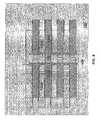
- FIGS. 1-9show steps in a method of making a grid of vias according to an embodiment described herein.
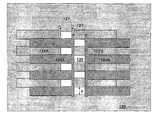
- FIG. 1illustrates a top down view and FIG. 2 shows a cut-away side view along line A-A of a mask 110 arranged over a stack of materials including a substrate 150 , a conductive material 140 layer, such as a metal or a metal silicide, a dielectric material 130 , such as an oxide, and a negative photoresist material 120 , such as SU-8.
- the conductive layer 140may include, for example, a single layer of conductive material or may include a plurality of conductive lines. It should be understood that the materials described for FIGS. 1 and 2 are examples only and the stack could include any number of different materials.
- the mask 110includes a plurality of apertures 112 A, 112 B formed therein.
- an “aperture”can refer to, for example, an opening extending partially or completely through the mask, or any other feature configured to purposefully allow certain radiation, or portions thereof, to pass through the mask.
- Each of the apertures 112 A, 112 Bincludes a plurality of finger apertures 114 joined by a cross-connecting aperture 116 arranged substantially perpendicularly to and at one edge of the finger apertures 114 .
- the apertures 112 A, 112 Beach have four finger apertures 114 .
- the apertures 112 A and 112 Bmay have fewer or a greater number of finger apertures 114 , for example, two, three, five, six, or more.
- the width of the fingers w, the width of the cross-connector aperture c, and the spacing between the apertures smay all be modified as desired.
- the width w of the finger apertures 114is greater than the width z of the portion of the mask 110 separating the finger apertures 114 .
- the shape of the finger apertures 114may be modified to change the shape of the final vias 132 ( FIG. 9 ).
- multiple pairs of corresponding apertures 1312 A, 1312 B, 1314 A, 1314 B, 1316 A, and 1316 Bcan be arranged in a single mask 1310 to form contacts at various locations on a single integrated circuit or on a number of integrated circuits arranged on a same die.
- the pattern shift for the two exposurescan also be used to adjust final via shape and size.
- the photoresist material 120is exposed to radiation, such as light, during a first exposure step.
- First portions 122 A, 122 B of the photoresist material 120 receiving certain radiation through the apertures 112 A, 112 B and areas outside the mask 110are formed into a pattern 121 ( FIG. 4 ) that remains substantially intact after the photoresist material 120 is treated, for example, by a solvent in a later step.
- FIG. 4shows the photoresist material 120 underneath the mask 110 . Areas 125 of the photoresist material 120 not exposed to the radiation will not be removed by a later step.
- the mask 110is shifted relative to the first pattern 121 so that, for example, the apertures 112 A, 112 B in the mask 110 overlap some part of the first portions 122 A, 122 B of the first pattern 121 .
- the mask 110is shifted to the right relative to the first pattern 121 by a distance X and down relative to the first pattern 121 by a distance Y.
- the photoresist material 120is exposed to radiation during a second exposure step.
- Second portions 124 A, 124 B of the photoresist material 120 receiving certain radiation through the apertures 112 A, 112 Bare formed into a second pattern 123 , overlapping the first portions 122 A, 122 B of the first pattern 121 , that remains substantially intact after treatment (e.g., developing).
- the mask 110( FIG. 6 ) is removed over from the photoresist material 120 .
- the unexposed portions 126 of the photoresist material 120 arranged between the first pattern 121 and second pattern 123are removable and form the footprints for the areas to be etched into vias. Due to the shifting of the mask, the height z of the unexposed portions 126 is equal to the distance z separating the horizontal apertures ( FIG. 1 ). Exposure, dose, and illumination will also influence height and width of unexposed regions. Adjustments or variation in the height of the unexposed portions z can be used to modify unexposed dimensions.
- the unexposed portions 126 ( FIG. 7 ) of the photoresist material 120are removed using methods known in the art, such as treating with a solvent, to form openings 128 in the photoresist material 120 to expose the dielectric material 130 .
- the dielectric material 130is then etched using the remaining photoresist material 120 as a mask, such as using either a wet or dry chemical etch to form the vias 132 in the dielectric material 130 and expose the conductive layer 140 .
- the remaining photoresist 120is removed to expose the dielectric material 130 having a plurality of vias 132 formed therein.
- the vias 132may then be filled with conductive material as is known in the art to form electrical connections to portions of the conductive layer 140 .
- the conductive layer 140may be made up of a plurality of closely spaced conductive lines (not shown) to which the conductive material in the vias 132 may be connected. Additional conductive materials or other features may be formed over the electrical connections.
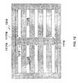
- FIGS. 10 , 11 , and 12each show further embodiments of masks 1010 , 1110 , 1210 , respectively, that may be used in the method described above in FIGS. 1-9 .
- the mask 1010 of FIG. 10includes a number of elongated apertures 1010 A, 1010 B, separated by and extending away from a central solid portion 1016 of the mask 1010 .
- the mask 1110 of FIG. 11includes a number of elongated apertures 1112 A, 1112 B, extending away from a central solid portion 1116 of the mask 1110 , and joined together at one end by a connecting aperture portion 1117 A, 11117 B.
- the mask 1210 of FIG. 12is similar to the mask 1110 of FIG. 11 , except that it also includes a number of protrusions 1218 arranged at the intersection of the apertures 1110 A, 1110 B and the central portion 1116 .
- the limitations imposed on the size of patterns made by photolithographic techniquesmay be overcome and patterns smaller than the minimum pitch for a given mask may be produced.
- the patternsmay then be formed into features such as vias and filled with conductive material to form electrical connections that are smaller than connections that could be produced using a single mask.
Landscapes
- Physics & Mathematics (AREA)
- General Physics & Mathematics (AREA)
- Engineering & Computer Science (AREA)
- Condensed Matter Physics & Semiconductors (AREA)
- Manufacturing & Machinery (AREA)
- Computer Hardware Design (AREA)
- Microelectronics & Electronic Packaging (AREA)
- Power Engineering (AREA)
- Preparing Plates And Mask In Photomechanical Process (AREA)
- Internal Circuitry In Semiconductor Integrated Circuit Devices (AREA)
- Exposure And Positioning Against Photoresist Photosensitive Materials (AREA)
Abstract
Description
Claims (20)
Priority Applications (1)
| Application Number | Priority Date | Filing Date | Title |
|---|---|---|---|
| US13/963,096US8685630B2 (en) | 2010-06-14 | 2013-08-09 | Methods of forming a pattern in a material and methods of forming openings in a material to be patterned |
Applications Claiming Priority (2)
| Application Number | Priority Date | Filing Date | Title |
|---|---|---|---|
| US12/815,181US8512938B2 (en) | 2010-06-14 | 2010-06-14 | Methods of forming a pattern in a material and methods of forming openings in a material to be patterned |
| US13/963,096US8685630B2 (en) | 2010-06-14 | 2013-08-09 | Methods of forming a pattern in a material and methods of forming openings in a material to be patterned |
Related Parent Applications (1)
| Application Number | Title | Priority Date | Filing Date |
|---|---|---|---|
| US12/815,181ContinuationUS8512938B2 (en) | 2010-06-14 | 2010-06-14 | Methods of forming a pattern in a material and methods of forming openings in a material to be patterned |
Publications (2)
| Publication Number | Publication Date |
|---|---|
| US20130323924A1 US20130323924A1 (en) | 2013-12-05 |
| US8685630B2true US8685630B2 (en) | 2014-04-01 |
Family
ID=45096490
Family Applications (2)
| Application Number | Title | Priority Date | Filing Date |
|---|---|---|---|
| US12/815,181Active2031-05-05US8512938B2 (en) | 2010-06-14 | 2010-06-14 | Methods of forming a pattern in a material and methods of forming openings in a material to be patterned |
| US13/963,096ActiveUS8685630B2 (en) | 2010-06-14 | 2013-08-09 | Methods of forming a pattern in a material and methods of forming openings in a material to be patterned |
Family Applications Before (1)
| Application Number | Title | Priority Date | Filing Date |
|---|---|---|---|
| US12/815,181Active2031-05-05US8512938B2 (en) | 2010-06-14 | 2010-06-14 | Methods of forming a pattern in a material and methods of forming openings in a material to be patterned |
Country Status (1)
| Country | Link |
|---|---|
| US (2) | US8512938B2 (en) |
Families Citing this family (3)
| Publication number | Priority date | Publication date | Assignee | Title |
|---|---|---|---|---|
| JP6617067B2 (en) | 2016-03-30 | 2019-12-04 | 日東電工株式会社 | Wiring circuit board and manufacturing method thereof |
| JP6795323B2 (en) | 2016-04-07 | 2020-12-02 | 日東電工株式会社 | Wiring circuit board and its manufacturing method |
| JP6787693B2 (en)* | 2016-06-07 | 2020-11-18 | 日東電工株式会社 | Wiring circuit board manufacturing method |
Citations (8)
| Publication number | Priority date | Publication date | Assignee | Title |
|---|---|---|---|---|
| US6934007B2 (en) | 2002-05-29 | 2005-08-23 | Massachusetts Institute Of Technology | Method for photolithography using multiple illuminations and a single fine feature mask |
| US20060181665A1 (en) | 2003-05-14 | 2006-08-17 | Obayashiseikou Co., Ltd. | High quality and ultra large screen liquid crystal display device and production method thereof |
| US7247574B2 (en) | 2003-01-14 | 2007-07-24 | Asml Masktools B.V. | Method and apparatus for providing optical proximity features to a reticle pattern for deep sub-wavelength optical lithography |
| US20070218673A1 (en) | 2006-03-15 | 2007-09-20 | Hiroko Nakamura | Manufacturing method of semiconductor device, reticle correcting method, and reticle pattern data correcting method |
| US20070238308A1 (en) | 2006-04-07 | 2007-10-11 | Ardavan Niroomand | Simplified pitch doubling process flow |
| US20090142932A1 (en) | 2007-11-29 | 2009-06-04 | Hynix Semiconductor Inc. | Method of forming a hard mask pattern in a semiconductor device |
| US20090258318A1 (en) | 2008-04-11 | 2009-10-15 | Sandisk 3D Llc | Double patterning method |
| US20100035192A1 (en) | 2008-08-06 | 2010-02-11 | Tokyo Ohka Kogyo Co., Ltd. | Method of forming resist pattern |
- 2010
- 2010-06-14USUS12/815,181patent/US8512938B2/enactiveActive
- 2013
- 2013-08-09USUS13/963,096patent/US8685630B2/enactiveActive
Patent Citations (8)
| Publication number | Priority date | Publication date | Assignee | Title |
|---|---|---|---|---|
| US6934007B2 (en) | 2002-05-29 | 2005-08-23 | Massachusetts Institute Of Technology | Method for photolithography using multiple illuminations and a single fine feature mask |
| US7247574B2 (en) | 2003-01-14 | 2007-07-24 | Asml Masktools B.V. | Method and apparatus for providing optical proximity features to a reticle pattern for deep sub-wavelength optical lithography |
| US20060181665A1 (en) | 2003-05-14 | 2006-08-17 | Obayashiseikou Co., Ltd. | High quality and ultra large screen liquid crystal display device and production method thereof |
| US20070218673A1 (en) | 2006-03-15 | 2007-09-20 | Hiroko Nakamura | Manufacturing method of semiconductor device, reticle correcting method, and reticle pattern data correcting method |
| US20070238308A1 (en) | 2006-04-07 | 2007-10-11 | Ardavan Niroomand | Simplified pitch doubling process flow |
| US20090142932A1 (en) | 2007-11-29 | 2009-06-04 | Hynix Semiconductor Inc. | Method of forming a hard mask pattern in a semiconductor device |
| US20090258318A1 (en) | 2008-04-11 | 2009-10-15 | Sandisk 3D Llc | Double patterning method |
| US20100035192A1 (en) | 2008-08-06 | 2010-02-11 | Tokyo Ohka Kogyo Co., Ltd. | Method of forming resist pattern |
Also Published As
| Publication number | Publication date |
|---|---|
| US20130323924A1 (en) | 2013-12-05 |
| US20110305997A1 (en) | 2011-12-15 |
| US8512938B2 (en) | 2013-08-20 |
Similar Documents
| Publication | Publication Date | Title |
|---|---|---|
| US8808971B2 (en) | Method for forming fine patterns of semiconductor device | |
| TWI452628B (en) | Method for fabricating a pattern on a wafer by an exposure process | |
| JP4536314B2 (en) | Semiconductor memory device and manufacturing method of semiconductor memory device | |
| US8685630B2 (en) | Methods of forming a pattern in a material and methods of forming openings in a material to be patterned | |
| US8871407B2 (en) | Patterning mask and method of formation of mask using step double patterning | |
| KR100464860B1 (en) | Method for forming photoresist pattern and method for forming capacitor using the same and capacitor | |
| US10818504B2 (en) | Method for producing a pattern of features by lithography and etching | |
| US6670109B2 (en) | Photolithographic methods of using a single reticle to form overlapping patterns | |
| KR100942074B1 (en) | Method of forming fine pattern of semiconductor device | |
| KR101052929B1 (en) | How to form a pattern on a wafer by exposure process | |
| US20090317979A1 (en) | Method for patterning an active region in a semiconductor device using a space patterning process | |
| US8420453B2 (en) | Method of forming active region structure | |
| US7063921B2 (en) | Photomask, in particular alternating phase shift mask, with compensation structure | |
| US20110171821A1 (en) | Semiconductor Devices and Methods of Manufacturing Thereof | |
| US20070082472A1 (en) | Method of manufacturing contact hole | |
| KR100192928B1 (en) | Open bit line semiconductor device | |
| KR100290588B1 (en) | Method for forming conductive film pattern in semiconductor device | |
| US20040048469A1 (en) | Hole forming by cross-shape image exposure | |
| KR100674898B1 (en) | Manufacturing Method of Semiconductor Memory Device | |
| TW202305872A (en) | Photomask and manufacturing method of interconnect | |
| US20030215752A1 (en) | Device manufacturing method | |
| KR101037539B1 (en) | Semiconductor element and formation method thereof | |
| KR20090069770A (en) | Manufacturing method of phase change memory device having fine contact hole | |
| KR20080000445A (en) | Photo mask for slit type contact and pattern manufacturing method using same | |
| KR19990057885A (en) | Pattern forming mask to prevent spacer collapse |
Legal Events
| Date | Code | Title | Description |
|---|---|---|---|
| FEPP | Fee payment procedure | Free format text:PAYOR NUMBER ASSIGNED (ORIGINAL EVENT CODE: ASPN); ENTITY STATUS OF PATENT OWNER: LARGE ENTITY | |
| STCF | Information on status: patent grant | Free format text:PATENTED CASE | |
| AS | Assignment | Owner name:U.S. BANK NATIONAL ASSOCIATION, AS COLLATERAL AGENT, CALIFORNIA Free format text:SECURITY INTEREST;ASSIGNOR:MICRON TECHNOLOGY, INC.;REEL/FRAME:038669/0001 Effective date:20160426 Owner name:U.S. BANK NATIONAL ASSOCIATION, AS COLLATERAL AGEN Free format text:SECURITY INTEREST;ASSIGNOR:MICRON TECHNOLOGY, INC.;REEL/FRAME:038669/0001 Effective date:20160426 | |
| AS | Assignment | Owner name:MORGAN STANLEY SENIOR FUNDING, INC., AS COLLATERAL AGENT, MARYLAND Free format text:PATENT SECURITY AGREEMENT;ASSIGNOR:MICRON TECHNOLOGY, INC.;REEL/FRAME:038954/0001 Effective date:20160426 Owner name:MORGAN STANLEY SENIOR FUNDING, INC., AS COLLATERAL Free format text:PATENT SECURITY AGREEMENT;ASSIGNOR:MICRON TECHNOLOGY, INC.;REEL/FRAME:038954/0001 Effective date:20160426 | |
| AS | Assignment | Owner name:U.S. BANK NATIONAL ASSOCIATION, AS COLLATERAL AGENT, CALIFORNIA Free format text:CORRECTIVE ASSIGNMENT TO CORRECT THE REPLACE ERRONEOUSLY FILED PATENT #7358718 WITH THE CORRECT PATENT #7358178 PREVIOUSLY RECORDED ON REEL 038669 FRAME 0001. ASSIGNOR(S) HEREBY CONFIRMS THE SECURITY INTEREST;ASSIGNOR:MICRON TECHNOLOGY, INC.;REEL/FRAME:043079/0001 Effective date:20160426 Owner name:U.S. BANK NATIONAL ASSOCIATION, AS COLLATERAL AGEN Free format text:CORRECTIVE ASSIGNMENT TO CORRECT THE REPLACE ERRONEOUSLY FILED PATENT #7358718 WITH THE CORRECT PATENT #7358178 PREVIOUSLY RECORDED ON REEL 038669 FRAME 0001. ASSIGNOR(S) HEREBY CONFIRMS THE SECURITY INTEREST;ASSIGNOR:MICRON TECHNOLOGY, INC.;REEL/FRAME:043079/0001 Effective date:20160426 | |
| MAFP | Maintenance fee payment | Free format text:PAYMENT OF MAINTENANCE FEE, 4TH YEAR, LARGE ENTITY (ORIGINAL EVENT CODE: M1551) Year of fee payment:4 | |
| AS | Assignment | Owner name:JPMORGAN CHASE BANK, N.A., AS COLLATERAL AGENT, ILLINOIS Free format text:SECURITY INTEREST;ASSIGNORS:MICRON TECHNOLOGY, INC.;MICRON SEMICONDUCTOR PRODUCTS, INC.;REEL/FRAME:047540/0001 Effective date:20180703 Owner name:JPMORGAN CHASE BANK, N.A., AS COLLATERAL AGENT, IL Free format text:SECURITY INTEREST;ASSIGNORS:MICRON TECHNOLOGY, INC.;MICRON SEMICONDUCTOR PRODUCTS, INC.;REEL/FRAME:047540/0001 Effective date:20180703 | |
| AS | Assignment | Owner name:MICRON TECHNOLOGY, INC., IDAHO Free format text:RELEASE BY SECURED PARTY;ASSIGNOR:U.S. BANK NATIONAL ASSOCIATION, AS COLLATERAL AGENT;REEL/FRAME:047243/0001 Effective date:20180629 | |
| AS | Assignment | Owner name:MICRON TECHNOLOGY, INC., IDAHO Free format text:RELEASE BY SECURED PARTY;ASSIGNOR:MORGAN STANLEY SENIOR FUNDING, INC., AS COLLATERAL AGENT;REEL/FRAME:050937/0001 Effective date:20190731 | |
| AS | Assignment | Owner name:MICRON TECHNOLOGY, INC., IDAHO Free format text:RELEASE BY SECURED PARTY;ASSIGNOR:JPMORGAN CHASE BANK, N.A., AS COLLATERAL AGENT;REEL/FRAME:051028/0001 Effective date:20190731 Owner name:MICRON SEMICONDUCTOR PRODUCTS, INC., IDAHO Free format text:RELEASE BY SECURED PARTY;ASSIGNOR:JPMORGAN CHASE BANK, N.A., AS COLLATERAL AGENT;REEL/FRAME:051028/0001 Effective date:20190731 | |
| MAFP | Maintenance fee payment | Free format text:PAYMENT OF MAINTENANCE FEE, 8TH YEAR, LARGE ENTITY (ORIGINAL EVENT CODE: M1552); ENTITY STATUS OF PATENT OWNER: LARGE ENTITY Year of fee payment:8 | |
| MAFP | Maintenance fee payment | Free format text:PAYMENT OF MAINTENANCE FEE, 12TH YEAR, LARGE ENTITY (ORIGINAL EVENT CODE: M1553); ENTITY STATUS OF PATENT OWNER: LARGE ENTITY Year of fee payment:12 |