US8685549B2 - Nanocomposites for ultra high density information storage, devices including the same, and methods of making the same - Google Patents
Nanocomposites for ultra high density information storage, devices including the same, and methods of making the sameDownload PDFInfo
- Publication number
- US8685549B2 US8685549B2US12/956,598US95659810AUS8685549B2US 8685549 B2US8685549 B2US 8685549B2US 95659810 AUS95659810 AUS 95659810AUS 8685549 B2US8685549 B2US 8685549B2
- Authority
- US
- United States
- Prior art keywords
- phase
- magnetic
- ordered
- substrate
- crystalline
- Prior art date
- Legal status (The legal status is an assumption and is not a legal conclusion. Google has not performed a legal analysis and makes no representation as to the accuracy of the status listed.)
- Active, expires
Links
- 239000002114nanocompositeSubstances0.000titleclaimsabstractdescription53
- 238000003860storageMethods0.000titleclaimsabstractdescription11
- 238000000034methodMethods0.000titleclaimsdescription94
- 239000000758substrateSubstances0.000claimsabstractdescription112
- 230000005291magnetic effectEffects0.000claimsabstractdescription109
- 239000002086nanomaterialSubstances0.000claimsabstractdescription61
- 239000011159matrix materialSubstances0.000claimsabstractdescription52
- 239000000696magnetic materialSubstances0.000claimsabstractdescription37
- 239000013078crystalSubstances0.000claimsabstractdescription22
- 238000013500data storageMethods0.000claimsabstractdescription14
- 229910001233yttria-stabilized zirconiaInorganic materials0.000claimsdescription58
- 238000000151depositionMethods0.000claimsdescription52
- 238000004544sputter depositionMethods0.000claimsdescription51
- 239000000463materialSubstances0.000claimsdescription26
- 230000008021depositionEffects0.000claimsdescription20
- 238000005229chemical vapour depositionMethods0.000claimsdescription12
- 230000015572biosynthetic processEffects0.000claimsdescription11
- 229910052751metalInorganic materials0.000claimsdescription11
- 239000002184metalSubstances0.000claimsdescription11
- 239000000203mixtureSubstances0.000claimsdescription10
- 238000005137deposition processMethods0.000claimsdescription9
- 230000005294ferromagnetic effectEffects0.000claimsdescription9
- 229910052710siliconInorganic materials0.000claimsdescription5
- 239000010703siliconSubstances0.000claimsdescription5
- 238000010549co-EvaporationMethods0.000claimsdescription4
- 238000000608laser ablationMethods0.000claimsdescription4
- FAPWRFPIFSIZLT-UHFFFAOYSA-MSodium chlorideChemical compound[Na+].[Cl-]FAPWRFPIFSIZLT-UHFFFAOYSA-M0.000claimsdescription3
- 150000001875compoundsChemical class0.000claimsdescription3
- 150000001247metal acetylidesChemical class0.000claimsdescription3
- 150000004767nitridesChemical class0.000claimsdescription3
- 235000002639sodium chlorideNutrition0.000claimsdescription3
- 239000011780sodium chlorideSubstances0.000claimsdescription3
- 229910052984zinc sulfideInorganic materials0.000claimsdescription3
- 238000004519manufacturing processMethods0.000abstractdescription6
- 239000010410layerSubstances0.000description111
- 239000002070nanowireSubstances0.000description53
- 239000012071phaseSubstances0.000description51
- 239000013077target materialSubstances0.000description23
- 230000008569processEffects0.000description22
- 239000010408filmSubstances0.000description21
- 239000007789gasSubstances0.000description14
- 238000001755magnetron sputter depositionMethods0.000description14
- 238000000137annealingMethods0.000description13
- 230000005415magnetizationEffects0.000description13
- PXHVJJICTQNCMI-UHFFFAOYSA-NNickelChemical compound[Ni]PXHVJJICTQNCMI-UHFFFAOYSA-N0.000description9
- -1nanodotsSubstances0.000description9
- 239000002073nanorodSubstances0.000description8
- 238000004549pulsed laser depositionMethods0.000description8
- 238000005546reactive sputteringMethods0.000description8
- 239000000126substanceSubstances0.000description8
- 238000004627transmission electron microscopyMethods0.000description8
- 238000002441X-ray diffractionMethods0.000description7
- 230000006870functionEffects0.000description7
- 229910052760oxygenInorganic materials0.000description7
- 230000004044responseEffects0.000description7
- 238000005096rolling processMethods0.000description7
- 238000004458analytical methodMethods0.000description6
- 230000001419dependent effectEffects0.000description6
- 238000010438heat treatmentMethods0.000description6
- 238000007735ion beam assisted depositionMethods0.000description6
- 238000012805post-processingMethods0.000description6
- 230000004888barrier functionEffects0.000description5
- 230000000903blocking effectEffects0.000description5
- CETPSERCERDGAM-UHFFFAOYSA-Nceric oxideChemical compoundO=[Ce]=OCETPSERCERDGAM-UHFFFAOYSA-N0.000description5
- 229910000422cerium(IV) oxideInorganic materials0.000description5
- 229910017052cobaltInorganic materials0.000description5
- 239000010941cobaltSubstances0.000description5
- GUTLYIVDDKVIGB-UHFFFAOYSA-Ncobalt atomChemical compound[Co]GUTLYIVDDKVIGB-UHFFFAOYSA-N0.000description5
- 238000009826distributionMethods0.000description5
- 238000002149energy-dispersive X-ray emission spectroscopyMethods0.000description5
- 229910052759nickelInorganic materials0.000description5
- IJGRMHOSHXDMSA-UHFFFAOYSA-NAtomic nitrogenChemical compoundN#NIJGRMHOSHXDMSA-UHFFFAOYSA-N0.000description4
- XUIMIQQOPSSXEZ-UHFFFAOYSA-NSiliconChemical compound[Si]XUIMIQQOPSSXEZ-UHFFFAOYSA-N0.000description4
- 238000002679ablationMethods0.000description4
- 239000000835fiberSubstances0.000description4
- 239000001257hydrogenSubstances0.000description4
- 229910052739hydrogenInorganic materials0.000description4
- 238000005259measurementMethods0.000description4
- 239000001301oxygenSubstances0.000description4
- 239000002245particleSubstances0.000description4
- 238000012545processingMethods0.000description4
- RUDFQVOCFDJEEF-UHFFFAOYSA-Nyttrium(III) oxideInorganic materials[O-2].[O-2].[O-2].[Y+3].[Y+3]RUDFQVOCFDJEEF-UHFFFAOYSA-N0.000description4
- QGZKDVFQNNGYKY-UHFFFAOYSA-NAmmoniaChemical compoundNQGZKDVFQNNGYKY-UHFFFAOYSA-N0.000description3
- CURLTUGMZLYLDI-UHFFFAOYSA-NCarbon dioxideChemical compoundO=C=OCURLTUGMZLYLDI-UHFFFAOYSA-N0.000description3
- CPLXHLVBOLITMK-UHFFFAOYSA-NMagnesium oxideChemical compound[Mg]=OCPLXHLVBOLITMK-UHFFFAOYSA-N0.000description3
- MWUXSHHQAYIFBG-UHFFFAOYSA-NNitric oxideChemical compoundO=[N]MWUXSHHQAYIFBG-UHFFFAOYSA-N0.000description3
- 229910045601alloyInorganic materials0.000description3
- 239000000956alloySubstances0.000description3
- PNEYBMLMFCGWSK-UHFFFAOYSA-Naluminium oxideInorganic materials[O-2].[O-2].[O-2].[Al+3].[Al+3]PNEYBMLMFCGWSK-UHFFFAOYSA-N0.000description3
- 238000013459approachMethods0.000description3
- QVGXLLKOCUKJST-UHFFFAOYSA-Natomic oxygenChemical compound[O]QVGXLLKOCUKJST-UHFFFAOYSA-N0.000description3
- 239000002131composite materialSubstances0.000description3
- 229910052802copperInorganic materials0.000description3
- 239000010949copperSubstances0.000description3
- 229910052593corundumInorganic materials0.000description3
- 230000003247decreasing effectEffects0.000description3
- 230000007547defectEffects0.000description3
- 230000000694effectsEffects0.000description3
- 238000005516engineering processMethods0.000description3
- 238000011066ex-situ storageMethods0.000description3
- 239000011261inert gasSubstances0.000description3
- 239000002105nanoparticleSubstances0.000description3
- 238000001552radio frequency sputter depositionMethods0.000description3
- 238000000851scanning transmission electron micrographMethods0.000description3
- XLYOFNOQVPJJNP-UHFFFAOYSA-NwaterSubstancesOXLYOFNOQVPJJNP-UHFFFAOYSA-N0.000description3
- 229910001845yogo sapphireInorganic materials0.000description3
- 229910052727yttriumInorganic materials0.000description3
- 229910052726zirconiumInorganic materials0.000description3
- XKRFYHLGVUSROY-UHFFFAOYSA-NArgonChemical compound[Ar]XKRFYHLGVUSROY-UHFFFAOYSA-N0.000description2
- UGFAIRIUMAVXCW-UHFFFAOYSA-NCarbon monoxideChemical compound[O+]#[C-]UGFAIRIUMAVXCW-UHFFFAOYSA-N0.000description2
- YCKRFDGAMUMZLT-UHFFFAOYSA-NFluorine atomChemical compound[F]YCKRFDGAMUMZLT-UHFFFAOYSA-N0.000description2
- XEEYBQQBJWHFJM-UHFFFAOYSA-NIronChemical compound[Fe]XEEYBQQBJWHFJM-UHFFFAOYSA-N0.000description2
- 238000003917TEM imageMethods0.000description2
- MCMNRKCIXSYSNV-UHFFFAOYSA-NZirconium dioxideChemical compoundO=[Zr]=OMCMNRKCIXSYSNV-UHFFFAOYSA-N0.000description2
- 229910052786argonInorganic materials0.000description2
- 125000004429atomChemical group0.000description2
- 230000008901benefitEffects0.000description2
- 229910002092carbon dioxideInorganic materials0.000description2
- 239000001569carbon dioxideSubstances0.000description2
- 229910002091carbon monoxideInorganic materials0.000description2
- 239000000919ceramicSubstances0.000description2
- 238000006243chemical reactionMethods0.000description2
- 239000011248coating agentSubstances0.000description2
- 238000000576coating methodMethods0.000description2
- 238000001816coolingMethods0.000description2
- 238000013461designMethods0.000description2
- 238000009792diffusion processMethods0.000description2
- 239000011737fluorineSubstances0.000description2
- 229910052731fluorineInorganic materials0.000description2
- 239000011888foilSubstances0.000description2
- 229910000856hastalloyInorganic materials0.000description2
- 238000000168high power impulse magnetron sputter depositionMethods0.000description2
- 238000002173high-resolution transmission electron microscopyMethods0.000description2
- 238000011065in-situ storageMethods0.000description2
- 230000003993interactionEffects0.000description2
- 238000001659ion-beam spectroscopyMethods0.000description2
- 150000002500ionsChemical class0.000description2
- 229910052746lanthanumInorganic materials0.000description2
- FZLIPJUXYLNCLC-UHFFFAOYSA-Nlanthanum atomChemical compound[La]FZLIPJUXYLNCLC-UHFFFAOYSA-N0.000description2
- 239000002071nanotubeSubstances0.000description2
- 229910052757nitrogenInorganic materials0.000description2
- 229910052763palladiumInorganic materials0.000description2
- 230000037361pathwayEffects0.000description2
- 229910052697platinumInorganic materials0.000description2
- 230000005855radiationEffects0.000description2
- 238000001350scanning transmission electron microscopyMethods0.000description2
- 229910052709silverInorganic materials0.000description2
- 239000010409thin filmSubstances0.000description2
- 230000007704transitionEffects0.000description2
- QYEXBYZXHDUPRC-UHFFFAOYSA-NB#[Ti]#BChemical compoundB#[Ti]#BQYEXBYZXHDUPRC-UHFFFAOYSA-N0.000description1
- 239000004215Carbon black (E152)Substances0.000description1
- 229910052684CeriumInorganic materials0.000description1
- RYGMFSIKBFXOCR-UHFFFAOYSA-NCopperChemical compound[Cu]RYGMFSIKBFXOCR-UHFFFAOYSA-N0.000description1
- 229910052692DysprosiumInorganic materials0.000description1
- 229910052691ErbiumInorganic materials0.000description1
- 229910052693EuropiumInorganic materials0.000description1
- 229910052688GadoliniumInorganic materials0.000description1
- 229910052689HolmiumInorganic materials0.000description1
- 229910002230La2Zr2O7Inorganic materials0.000description1
- 229910002244LaAlO3Inorganic materials0.000description1
- 229910002262LaCrO3Inorganic materials0.000description1
- 229910002331LaGaO3Inorganic materials0.000description1
- 229910002328LaMnO3Inorganic materials0.000description1
- 229910002340LaNiO3Inorganic materials0.000description1
- 229910052765LutetiumInorganic materials0.000description1
- 229910003200NdGaO3Inorganic materials0.000description1
- 229910052779NeodymiumInorganic materials0.000description1
- GQPLMRYTRLFLPF-UHFFFAOYSA-NNitrous OxideChemical compound[O-][N+]#NGQPLMRYTRLFLPF-UHFFFAOYSA-N0.000description1
- CBENFWSGALASAD-UHFFFAOYSA-NOzoneChemical compound[O-][O+]=OCBENFWSGALASAD-UHFFFAOYSA-N0.000description1
- 229910052777PraseodymiumInorganic materials0.000description1
- 229910052772SamariumInorganic materials0.000description1
- 229910002370SrTiO3Inorganic materials0.000description1
- 229910052771TerbiumInorganic materials0.000description1
- 229910052775ThuliumInorganic materials0.000description1
- 229910033181TiB2Inorganic materials0.000description1
- ATJFFYVFTNAWJD-UHFFFAOYSA-NTinChemical compound[Sn]ATJFFYVFTNAWJD-UHFFFAOYSA-N0.000description1
- 229910052769YtterbiumInorganic materials0.000description1
- YCANCZRRZBHLEN-UHFFFAOYSA-N[N].OChemical compound[N].OYCANCZRRZBHLEN-UHFFFAOYSA-N0.000description1
- PWKWDCOTNGQLID-UHFFFAOYSA-N[N].[Ar]Chemical compound[N].[Ar]PWKWDCOTNGQLID-UHFFFAOYSA-N0.000description1
- VVTSZOCINPYFDP-UHFFFAOYSA-N[O].[Ar]Chemical compound[O].[Ar]VVTSZOCINPYFDP-UHFFFAOYSA-N0.000description1
- 230000001133accelerationEffects0.000description1
- 229910000287alkaline earth metal oxideInorganic materials0.000description1
- 229910052782aluminiumInorganic materials0.000description1
- 229910021529ammoniaInorganic materials0.000description1
- CMBZEFASPGWDEN-UHFFFAOYSA-Nargon;hydrateChemical compoundO.[Ar]CMBZEFASPGWDEN-UHFFFAOYSA-N0.000description1
- 238000003491arrayMethods0.000description1
- 229910001632barium fluorideInorganic materials0.000description1
- JRPBQTZRNDNNOP-UHFFFAOYSA-Nbarium titanateChemical compound[Ba+2].[Ba+2].[O-][Ti]([O-])([O-])[O-]JRPBQTZRNDNNOP-UHFFFAOYSA-N0.000description1
- 229910002113barium titanateInorganic materials0.000description1
- 229910021523barium zirconateInorganic materials0.000description1
- DQBAOWPVHRWLJC-UHFFFAOYSA-Nbarium(2+);dioxido(oxo)zirconiumChemical compound[Ba+2].[O-][Zr]([O-])=ODQBAOWPVHRWLJC-UHFFFAOYSA-N0.000description1
- 230000005540biological transmissionEffects0.000description1
- 238000009529body temperature measurementMethods0.000description1
- 238000004364calculation methodMethods0.000description1
- GWXLDORMOJMVQZ-UHFFFAOYSA-NceriumChemical compound[Ce]GWXLDORMOJMVQZ-UHFFFAOYSA-N0.000description1
- 239000003795chemical substances by applicationSubstances0.000description1
- 230000007797corrosionEffects0.000description1
- 238000005260corrosionMethods0.000description1
- 230000008878couplingEffects0.000description1
- 238000010168coupling processMethods0.000description1
- 238000005859coupling reactionMethods0.000description1
- 229910021419crystalline siliconInorganic materials0.000description1
- 238000011161developmentMethods0.000description1
- RWRIWBAIICGTTQ-UHFFFAOYSA-NdifluoromethaneChemical compoundFCFRWRIWBAIICGTTQ-UHFFFAOYSA-N0.000description1
- TXKMVPPZCYKFAC-UHFFFAOYSA-Ndisulfur monoxideInorganic materialsO=S=STXKMVPPZCYKFAC-UHFFFAOYSA-N0.000description1
- KBQHZAAAGSGFKK-UHFFFAOYSA-Ndysprosium atomChemical compound[Dy]KBQHZAAAGSGFKK-UHFFFAOYSA-N0.000description1
- 238000004070electrodepositionMethods0.000description1
- 238000010894electron beam technologyMethods0.000description1
- UYAHIZSMUZPPFV-UHFFFAOYSA-NerbiumChemical compound[Er]UYAHIZSMUZPPFV-UHFFFAOYSA-N0.000description1
- OGPBJKLSAFTDLK-UHFFFAOYSA-Neuropium atomChemical compound[Eu]OGPBJKLSAFTDLK-UHFFFAOYSA-N0.000description1
- 239000007775ferroic materialSubstances0.000description1
- 239000000945fillerSubstances0.000description1
- NBVXSUQYWXRMNV-UHFFFAOYSA-NfluoromethaneChemical compoundFCNBVXSUQYWXRMNV-UHFFFAOYSA-N0.000description1
- UIWYJDYFSGRHKR-UHFFFAOYSA-Ngadolinium atomChemical compound[Gd]UIWYJDYFSGRHKR-UHFFFAOYSA-N0.000description1
- 229910052737goldInorganic materials0.000description1
- 239000001307heliumSubstances0.000description1
- 229910052734heliumInorganic materials0.000description1
- SWQJXJOGLNCZEY-UHFFFAOYSA-Nhelium atomChemical compound[He]SWQJXJOGLNCZEY-UHFFFAOYSA-N0.000description1
- 238000001534heteroepitaxyMethods0.000description1
- KJZYNXUDTRRSPN-UHFFFAOYSA-Nholmium atomChemical compound[Ho]KJZYNXUDTRRSPN-UHFFFAOYSA-N0.000description1
- 229930195733hydrocarbonNatural products0.000description1
- 150000002430hydrocarbonsChemical class0.000description1
- 150000002431hydrogenChemical class0.000description1
- 239000012433hydrogen halideSubstances0.000description1
- 229910000039hydrogen halideInorganic materials0.000description1
- 238000009413insulationMethods0.000description1
- 238000010884ion-beam techniqueMethods0.000description1
- 229910052742ironInorganic materials0.000description1
- 229910052743kryptonInorganic materials0.000description1
- DNNSSWSSYDEUBZ-UHFFFAOYSA-Nkrypton atomChemical compound[Kr]DNNSSWSSYDEUBZ-UHFFFAOYSA-N0.000description1
- HFGPZNIAWCZYJU-UHFFFAOYSA-Nlead zirconate titanateChemical compound[O-2].[O-2].[O-2].[O-2].[O-2].[Ti+4].[Zr+4].[Pb+2]HFGPZNIAWCZYJU-UHFFFAOYSA-N0.000description1
- 229910052451lead zirconate titanateInorganic materials0.000description1
- 239000007791liquid phaseSubstances0.000description1
- KLUYKAPZRJJIKT-UHFFFAOYSA-NlutetiumChemical compound[Lu][Lu]KLUYKAPZRJJIKT-UHFFFAOYSA-N0.000description1
- 239000006249magnetic particleSubstances0.000description1
- 230000007246mechanismEffects0.000description1
- 229910001092metal group alloyInorganic materials0.000description1
- 229910044991metal oxideInorganic materials0.000description1
- 150000004706metal oxidesChemical class0.000description1
- 150000002739metalsChemical class0.000description1
- DOTMOQHOJINYBL-UHFFFAOYSA-Nmolecular nitrogen;molecular oxygenChemical compoundN#N.O=ODOTMOQHOJINYBL-UHFFFAOYSA-N0.000description1
- 230000000877morphologic effectEffects0.000description1
- QEFYFXOXNSNQGX-UHFFFAOYSA-Nneodymium atomChemical compound[Nd]QEFYFXOXNSNQGX-UHFFFAOYSA-N0.000description1
- 229910052754neonInorganic materials0.000description1
- GKAOGPIIYCISHV-UHFFFAOYSA-Nneon atomChemical compound[Ne]GKAOGPIIYCISHV-UHFFFAOYSA-N0.000description1
- 229910000069nitrogen hydrideInorganic materials0.000description1
- 229910052756noble gasInorganic materials0.000description1
- 230000006911nucleationEffects0.000description1
- 238000010899nucleationMethods0.000description1
- 230000008520organizationEffects0.000description1
- 239000003973paintSubstances0.000description1
- 230000005298paramagnetic effectEffects0.000description1
- 230000000737periodic effectEffects0.000description1
- 238000005191phase separationMethods0.000description1
- 238000001020plasma etchingMethods0.000description1
- 239000004033plasticSubstances0.000description1
- 239000011148porous materialSubstances0.000description1
- PUDIUYLPXJFUGB-UHFFFAOYSA-Npraseodymium atomChemical compound[Pr]PUDIUYLPXJFUGB-UHFFFAOYSA-N0.000description1
- 239000002243precursorSubstances0.000description1
- 238000002360preparation methodMethods0.000description1
- 239000011241protective layerSubstances0.000description1
- 239000002096quantum dotSubstances0.000description1
- 229910052761rare earth metalInorganic materials0.000description1
- 150000002910rare earth metalsChemical class0.000description1
- 238000001953recrystallisationMethods0.000description1
- 238000011160researchMethods0.000description1
- 230000002441reversible effectEffects0.000description1
- 238000012552reviewMethods0.000description1
- 239000005060rubberSubstances0.000description1
- KZUNJOHGWZRPMI-UHFFFAOYSA-Nsamarium atomChemical compound[Sm]KZUNJOHGWZRPMI-UHFFFAOYSA-N0.000description1
- 238000013341scale-upMethods0.000description1
- 238000001338self-assemblyMethods0.000description1
- 239000004065semiconductorSubstances0.000description1
- 238000001228spectrumMethods0.000description1
- 238000005478sputtering typeMethods0.000description1
- 238000007619statistical methodMethods0.000description1
- XTQHKBHJIVJGKJ-UHFFFAOYSA-Nsulfur monoxideChemical compoundS=OXTQHKBHJIVJGKJ-UHFFFAOYSA-N0.000description1
- 239000002887superconductorSubstances0.000description1
- GZCRRIHWUXGPOV-UHFFFAOYSA-Nterbium atomChemical compound[Tb]GZCRRIHWUXGPOV-UHFFFAOYSA-N0.000description1
- 238000013169thromboelastometryMethods0.000description1
- FRNOGLGSGLTDKL-UHFFFAOYSA-Nthulium atomChemical compound[Tm]FRNOGLGSGLTDKL-UHFFFAOYSA-N0.000description1
- 229910052718tinInorganic materials0.000description1
- 238000009827uniform distributionMethods0.000description1
- 239000012808vapor phaseSubstances0.000description1
- 229910052724xenonInorganic materials0.000description1
- FHNFHKCVQCLJFQ-UHFFFAOYSA-Nxenon atomChemical compound[Xe]FHNFHKCVQCLJFQ-UHFFFAOYSA-N0.000description1
- NAWDYIZEMPQZHO-UHFFFAOYSA-NytterbiumChemical compound[Yb]NAWDYIZEMPQZHO-UHFFFAOYSA-N0.000description1
- VWQVUPCCIRVNHF-UHFFFAOYSA-Nyttrium atomChemical compound[Y]VWQVUPCCIRVNHF-UHFFFAOYSA-N0.000description1
Images


Classifications
- C—CHEMISTRY; METALLURGY
- C30—CRYSTAL GROWTH
- C30B—SINGLE-CRYSTAL GROWTH; UNIDIRECTIONAL SOLIDIFICATION OF EUTECTIC MATERIAL OR UNIDIRECTIONAL DEMIXING OF EUTECTOID MATERIAL; REFINING BY ZONE-MELTING OF MATERIAL; PRODUCTION OF A HOMOGENEOUS POLYCRYSTALLINE MATERIAL WITH DEFINED STRUCTURE; SINGLE CRYSTALS OR HOMOGENEOUS POLYCRYSTALLINE MATERIAL WITH DEFINED STRUCTURE; AFTER-TREATMENT OF SINGLE CRYSTALS OR A HOMOGENEOUS POLYCRYSTALLINE MATERIAL WITH DEFINED STRUCTURE; APPARATUS THEREFOR
- C30B23/00—Single-crystal growth by condensing evaporated or sublimed materials
- C30B23/02—Epitaxial-layer growth
- H—ELECTRICITY
- H01—ELECTRIC ELEMENTS
- H01F—MAGNETS; INDUCTANCES; TRANSFORMERS; SELECTION OF MATERIALS FOR THEIR MAGNETIC PROPERTIES
- H01F1/00—Magnets or magnetic bodies characterised by the magnetic materials therefor; Selection of materials for their magnetic properties
- H01F1/0036—Magnets or magnetic bodies characterised by the magnetic materials therefor; Selection of materials for their magnetic properties showing low dimensional magnetism, i.e. spin rearrangements due to a restriction of dimensions, e.g. showing giant magnetoresistivity
- H01F1/0045—Zero dimensional, e.g. nanoparticles, soft nanoparticles for medical/biological use
- H01F1/0063—Zero dimensional, e.g. nanoparticles, soft nanoparticles for medical/biological use in a non-magnetic matrix, e.g. granular solids
- H—ELECTRICITY
- H01—ELECTRIC ELEMENTS
- H01F—MAGNETS; INDUCTANCES; TRANSFORMERS; SELECTION OF MATERIALS FOR THEIR MAGNETIC PROPERTIES
- H01F1/00—Magnets or magnetic bodies characterised by the magnetic materials therefor; Selection of materials for their magnetic properties
- H01F1/0036—Magnets or magnetic bodies characterised by the magnetic materials therefor; Selection of materials for their magnetic properties showing low dimensional magnetism, i.e. spin rearrangements due to a restriction of dimensions, e.g. showing giant magnetoresistivity
- H01F1/0072—Magnets or magnetic bodies characterised by the magnetic materials therefor; Selection of materials for their magnetic properties showing low dimensional magnetism, i.e. spin rearrangements due to a restriction of dimensions, e.g. showing giant magnetoresistivity one dimensional, i.e. linear or dendritic nanostructures
- H01F1/0081—Magnets or magnetic bodies characterised by the magnetic materials therefor; Selection of materials for their magnetic properties showing low dimensional magnetism, i.e. spin rearrangements due to a restriction of dimensions, e.g. showing giant magnetoresistivity one dimensional, i.e. linear or dendritic nanostructures in a non-magnetic matrix, e.g. Fe-nanowires in a nanoporous membrane
- H—ELECTRICITY
- H01—ELECTRIC ELEMENTS
- H01F—MAGNETS; INDUCTANCES; TRANSFORMERS; SELECTION OF MATERIALS FOR THEIR MAGNETIC PROPERTIES
- H01F41/00—Apparatus or processes specially adapted for manufacturing or assembling magnets, inductances or transformers; Apparatus or processes specially adapted for manufacturing materials characterised by their magnetic properties
- H01F41/14—Apparatus or processes specially adapted for manufacturing or assembling magnets, inductances or transformers; Apparatus or processes specially adapted for manufacturing materials characterised by their magnetic properties for applying magnetic films to substrates
- H01F41/18—Apparatus or processes specially adapted for manufacturing or assembling magnets, inductances or transformers; Apparatus or processes specially adapted for manufacturing materials characterised by their magnetic properties for applying magnetic films to substrates by cathode sputtering
- H—ELECTRICITY
- H01—ELECTRIC ELEMENTS
- H01F—MAGNETS; INDUCTANCES; TRANSFORMERS; SELECTION OF MATERIALS FOR THEIR MAGNETIC PROPERTIES
- H01F41/00—Apparatus or processes specially adapted for manufacturing or assembling magnets, inductances or transformers; Apparatus or processes specially adapted for manufacturing materials characterised by their magnetic properties
- H01F41/14—Apparatus or processes specially adapted for manufacturing or assembling magnets, inductances or transformers; Apparatus or processes specially adapted for manufacturing materials characterised by their magnetic properties for applying magnetic films to substrates
- H01F41/20—Apparatus or processes specially adapted for manufacturing or assembling magnets, inductances or transformers; Apparatus or processes specially adapted for manufacturing materials characterised by their magnetic properties for applying magnetic films to substrates by evaporation
- Y—GENERAL TAGGING OF NEW TECHNOLOGICAL DEVELOPMENTS; GENERAL TAGGING OF CROSS-SECTIONAL TECHNOLOGIES SPANNING OVER SEVERAL SECTIONS OF THE IPC; TECHNICAL SUBJECTS COVERED BY FORMER USPC CROSS-REFERENCE ART COLLECTIONS [XRACs] AND DIGESTS
- Y10—TECHNICAL SUBJECTS COVERED BY FORMER USPC
- Y10T—TECHNICAL SUBJECTS COVERED BY FORMER US CLASSIFICATION
- Y10T428/00—Stock material or miscellaneous articles
- Y10T428/25—Web or sheet containing structurally defined element or component and including a second component containing structurally defined particles
- Y—GENERAL TAGGING OF NEW TECHNOLOGICAL DEVELOPMENTS; GENERAL TAGGING OF CROSS-SECTIONAL TECHNOLOGIES SPANNING OVER SEVERAL SECTIONS OF THE IPC; TECHNICAL SUBJECTS COVERED BY FORMER USPC CROSS-REFERENCE ART COLLECTIONS [XRACs] AND DIGESTS
- Y10—TECHNICAL SUBJECTS COVERED BY FORMER USPC
- Y10T—TECHNICAL SUBJECTS COVERED BY FORMER US CLASSIFICATION
- Y10T428/00—Stock material or miscellaneous articles
- Y10T428/29—Coated or structually defined flake, particle, cell, strand, strand portion, rod, filament, macroscopic fiber or mass thereof
- Y10T428/2913—Rod, strand, filament or fiber
- Y10T428/2918—Rod, strand, filament or fiber including free carbon or carbide or therewith [not as steel]
- Y10T428/292—In coating or impregnation
- Y—GENERAL TAGGING OF NEW TECHNOLOGICAL DEVELOPMENTS; GENERAL TAGGING OF CROSS-SECTIONAL TECHNOLOGIES SPANNING OVER SEVERAL SECTIONS OF THE IPC; TECHNICAL SUBJECTS COVERED BY FORMER USPC CROSS-REFERENCE ART COLLECTIONS [XRACs] AND DIGESTS
- Y10—TECHNICAL SUBJECTS COVERED BY FORMER USPC
- Y10T—TECHNICAL SUBJECTS COVERED BY FORMER US CLASSIFICATION
- Y10T428/00—Stock material or miscellaneous articles
- Y10T428/29—Coated or structually defined flake, particle, cell, strand, strand portion, rod, filament, macroscopic fiber or mass thereof
- Y10T428/2913—Rod, strand, filament or fiber
- Y10T428/2933—Coated or with bond, impregnation or core
- Y10T428/294—Coated or with bond, impregnation or core including metal or compound thereof [excluding glass, ceramic and asbestos]
- Y10T428/2958—Metal or metal compound in coating
Definitions
- the present inventionrelates to phase-separated, heteroepitaxial, ferroic materials for ultra high density information storage, devices including the same, and methods of making the same.
- magnetic nanostructuressuch as nanodots, nanotubes, nanowires, and nanocomposites for increasing magnetic disk drive capacities.
- a critical valuetypically a few tens of nanometer
- the magnetic anisotropy energy per particleis comparable to the thermal energy, resulting in superparamagnetic (SP) behavior above the blocking temperature (BT).
- SP nanoparticles embedded in an insulating matrixcan be magnetized rapidly by an external magnetic field with a lack of remanence and coercivity, properties which are attractive for magnetotransport and Coulomb blockade effect as well as biomedical applications due to their weak magnetic interaction.
- SP nanofeaturesare not suitable for magnetic data storage since beyond the “superparamagnetic limit,” thermal fluctuations at room temperature randomly flip the stored magnetic orientations.
- One approach reported for overcoming this limitationis to increase the magnetic anisotropy energy of the nanoparticles.
- Another approach reportedis to increase the magnetic anisotropy of zero-dimensional nanomaterials with the extension of one-dimension, for example, from nanodots to nanowires.
- One-dimensional arrays of pre-patterned perpendicular magnetic nanofeaturessuch as nanowires, nanotube, and nanorods embedded in a nonmagnetic matrix has therefore been extensively investigated as the next-generation technology for ultra-high density magnetic recording media applications requiring capacities over 500 gigabit/in 2 .
- a nanocomposite articlethat includes a single-crystal or single-crystal-like substrate and a heteroepitaxial, phase-separated layer supported by a surface of the substrate is described.
- the heteroepitaxial layercan include a continuous, non-magnetic, crystalline, matrix phase and an ordered magnetic phase disposed within the matrix phase.
- the ordered phasecan include a plurality of self-assembled crystalline nanostructures of a magnetic material.
- the ordered magnetic phasecan be discontinuous.
- the heteroepitaxial, phase-separated layercan include 1-99 vol-% of a non-magnetic material and 1-99 vol-% of a magnetic material.
- the single-crystal or single-crystal-like substratecan be silicon, e.g., silicon(100).
- the nanocomposite articlecan also include a butler layer disposed between the substrate and the phase-separated layer.
- the matrix phase and the buffer layercan have the same composition.
- the continuous, non-magnetic, crystalline, matrix phasecan include a material selected from the group consisting of oxides, nitrides, carbides, borides, and combination thereof.
- the continuous, non-magnetic, crystalline matrix phasecan include yttria-stabilized zirconia.
- the ordered magnetic phasecan include a ferromagnetic metal, a ferromagnetic compound, or both.
- the ordered magnetic phasecan include cobalt.
- An electronic storage devicethat includes a nanocomposite article as described herein and a read-write head for reading and/or writing information to the heteroepitaxial, phase-separated layer is also described.
- the read-write headcan be adapted for at least one of longitudinal reading/writing and perpendicular reading/writing.
- the recording or data storage density of the nanocomposite articlecan be at least 0.75 Tb/in 2 .
- a method of forming the nanocomposite article described hereinis also described.
- the methodcan include providing a single-crystal or single-crystal-like substrate having a surface and depositing the heteroepitaxial, phase-separated layer over the surface.
- the methodcan also include depositing a buffer layer over the substrate prior to depositing the heteroepitaxial layer.
- the depositing stepcan include simultaneous deposition of the continuous, non-magnetic, crystalline, matrix phase, and the ordered magnetic phase via an epitaxial formation technique.
- the depositing stepcan include an in-situ deposition process selected from the group consisting of pulsed laser ablation, chemical vapor deposition (CVD), metallorganic chemical vapor deposition (MOCVD), sputtering and e-beam co-evaporation.
- the depositing stepcomprises an ex-situ deposition process selected from the group consisting of chemical solution processes, pulsed laser ablation, chemical vapor deposition (CVD), metallorganic chemical vapor deposition (MOCVD), sputtering and e-beam co-evaporation, followed by a heat treatment.
- the target for the epitaxial formation techniquecan include a non-magnetic material and a magnetic material.
- the target for the epitaxial formation techniquecan include 1-99 vol-% of a non-magnetic material, and 1-99 vol-% of a magnetic material.
- FIGS. 1A-Care schematics showing the layered nanocomposite article according to the invention.
- FIG. 2is a schematic of the electronic storage device according to the invention.
- FIG. 3( a )Schematics: formation pathway of nanostructures dependent on the ablation ratio of Co to YSZ.
- FIG. 4( a )Cross-sectional STEM images of Co nanodots (top) and nanowires (bottom) embedded in YSZ matrices with EDS elementary maps of Co, Y, Zr, and O in the region defined in the left hand side STEM images.
- the size distribution of nanodotsthe frequency vs. the particle size.
- FIG. 5shows a TEM image of nanowires embedded in a matrix material and a statistical analysis of the diameter of the nanowires and the spacing between adjacent nanowires.
- FIG. 6shows hidh-resolution TEM cross-section images (top) and diffraction patterns (bottom) of Co nanodots (left) and nanowires (right) embedded in a YSZ matrix.
- FIG. 7shows XRD phi-scans for 111 reflections of Co nanostructures, 111 reflections of YSZ matrix and 111 reflections of Si substrate for nanodots (Sample A) and nanowires (Sample B).
- FIG. 9shows remanence, ZFC and FC magnetization data as a function of temperature for both (a) Co nanodots and (b) Co nanowires.
- a nanocomposite article useful for ultra high density data storagethat includes a plurality of crystalline, magnetic nanostructures disposed in an ordered manner within a non-magnetic matrix phase is described.
- a storage device including the nanocomposite article and a method of making the nanocomposite articleare also described.
- the inventorshave determined that it is possible to produce a structure that is sufficiently ordered to allow ultra high density data storage (0.75 Tb/in 2 or greater) through simultaneous deposition of the magnetic nanostructures and the non-magnetic matrix phase. This development opens the door for efficient production of materials for ultra high density data storage.
- a nanocomposite article 10that includes a single-crystal or single-crystal-like substrate 12 having a surface 14 and a heteroepitaxial, phase-separated layer 16 supported by the surface is described.
- the heteroepitaxial, phase-separated layer 16can include a continuous, non-magnetic, crystalline, matrix phase 18 , and an ordered magnetic phase 20 disposed within the matrix phase 20 .
- the ordered magnetic phase 20can be discontinuous.
- the ordered magnetic phase 20can include a plurality of self-assembled crystalline nanostructures of a magnetic material.
- the nanostructures 20can be nanodots, nanowires, nanorods, or combinations thereof.
- a first layeris “supported” on a second layer if the first layer is part of the same composite and is located above the second layer.
- a first layeris “deposited” on a second layer if the first layer is above and in contact with the second layer.
- a first layeris “supported” on a second layer, it is intended to encompass embodiments where the first layer is deposited on the second layer.
- the nanostructures 20can have a major axis aligned within 60 degrees of the c-axis of the phase-separated layer 16 , within 45 degrees of the c-axis, or within 30 degrees of the c-axis.
- the nanostructures 20can be arranged in columns through the thickness of the phase-separated layer 16 .
- the columns of nanostructures 20can be arranged at an angle ranging between 0 and 60 degrees relative to the c-axis of the phase-separated layer 16 , or between 0 and 45 degrees of the c-axis, or within 0 and 30 degrees of the c-axis.
- self-assembledrefers to a self-ordering process that occurs spontaneously during growth of the relevant layer or film. It will be understood that any of the phase-separated morphologies described herein can be self-assembled through a variety of epitaxial deposition processes.
- a unique aspect of the nanocomposite articles 10 described hereinis the self-assembled arrangement of the nanostructures 20 produces articles capable of a recording or data storage density of at least 0.75 Tb/in 2 , or at least 1 Tb/in 2 , at least 1.25 Tb/in 2 , or at least 1.5 Tb/in 2 .
- Thisis due in part to unique, unexpected result that the self-assembled nanostructures 20 in the phase-separated layer 16 described herein exhibit desirable paramagnetic properties for data storage, i.e., stable magnetic orientations and high remanent magnetization even at operating temperatures.
- suitable materials for the substrate 12include, but are not limited to, a single crystal substrate or a single crystal-like substrate.
- Exemplary single-crystal substrates 12include silicon(100) or silicon (001).
- Exemplary single-crystal-like substratesinclude, but are not limited to, rock-salt and Wurtzite crystal structures.
- the nanocomposite article 10can also include a buffer layer 22 disposed between the substrate 12 and the phase-separated layer 16 .
- Some or all of the buffer layers 22can be uniaxially textured [e.g., (100), (010), or (001)] or biaxially textured.
- Some or all of the buffer layers 22can be epitaxially deposited on the substrate 12 .
- the matrix phase 18 and the buffer layer 22can have the same composition, e.g., yttria-stabilized zirconia (YSZ), the same crystallographic orientations, or both.
- YSZyttria-stabilized zirconia
- biaxially texturedrefers to materials having crystallographic orientations both parallel and perpendicular to the basal plane of a material, e.g., ⁇ 100 ⁇ 100>, including texture aligned along a first axis along the [001] crystal direction, and along a second axis having a crystal direction selected from the group consisting of [111], [101], [113], [100], and [010].
- the degree of biaxial texture in the layer of which the biaxially textured surface, as specified by the FWHM of the out-of-plane and in-plane diffraction peak,is typically greater than 2° and less than 20°, preferably less than 15°, and optimally less than 10°.
- exemplary materials for the continuous, non-magnetic, crystalline, matrix phase 18include, but are not limited to, yttria-stabilized zirconia, barium zirconate, barium titanate, lead zirconate titanate, and combinations thereof.
- exemplary materials for the ordered magnetic phase 20include, but are not limited to cobalt, iron, nickel, oxides thereof, and combinations thereof.
- the continuous, non-magnetic, crystalline matrix phase 18 , the ordered magnetic phase 20 , or bothcan have a uniaxial crystallographic orientation, e.g., (100), (010) or (001), or a biaxial crystallographic orientation.
- the heteroepitaxial, phase-separated layer 16can include 1-99 vol-% of a non-magnetic material, 25-98 vol-% of a non-magnetic material, 50-97 vol-% of a non-magnetic material, 60-96 vol-% of a non-magnetic material, or any range defined by any of these end-points, e.g., 25-99 vol-% or 96-99 vol-%.
- the heteroepitaxial, phase-separated layer 16can include 1-99 vol-% of a magnetic material, 2-75 vol-% of a magnetic material, 3-50 vol-% a magnetic material, 4-40 vol-% of a magnetic material, or any range defined by any of these end-points, e.g., 2-40 vol-% or 1-4 vol-%.
- the ordered, magnetic phase 20can be embedded or partially embedded in the non-magnetic, crystalline matrix phase 18 .
- the ordered, magnetic phase 20can be present in the form of nanostructures, such as nanorods, nanodots, nanowires, and combinations thereof.
- the nanostructurescan be discontinuous, but present in an ordered array within the non-magnetic, crystalline, matrix phase.
- FIGS. 3( b ) and 4 ( a )show images of exemplary phase-separated materials where the ordered, magnetic phase is present as a plurality of nanodots and other exemplary phase-separated materials where the ordered, magnetic phase is present as a plurality of nanowires that are embedded or partially embedded in a continuous first phase of YSZ.
- the concentration or density of the nanostructures (i.e., nanorods, nanocolumns, nanodots and nanowires) in the non-magnetic, crystalline matrix phasecan vary.
- the number density of ordered magnetic nanostructurescan be between 400 and 4 ⁇ 10 4 per ⁇ m 2 , which corresponds to interspacing distance between adjacent nanostructures in the range of 5 to 50 nm in the phase-separated layer.
- the largest dimension (e.g., width or thickness) of the nanostructures 20 in the phase-separated layer 16can generally be of nanoscale dimensions, i.e., less than 1 ⁇ m.
- the largest dimension of the nanostructurescan be less than 500 nm, or less than 200 nm, or less than 100, 90, 80, 70, 60, 50, 40, 30, 20, or less than 10 nm.
- the smallest dimension of the nanostructurescan be at least 0.01, 0.1, 0.5, 1, 2, 3, 4, 5, 10, 20 or 30 nm.
- the nanostructurescan also have any combination of the aforesaid largest dimensions and smallest dimensions. However, smaller or larger thicknesses of the nanorod features are also possible. More typically, the largest dimension of the nanostructures is in the range of 1-100 nm, or 2-50 nm, or 3-40 nm.
- the diameter of the nanodotscan be between 1 nm and 50 nm.
- the diameter of the nanodotswill depend on the type of processes and processing conditions used to deposit the phase-separated layer. In the case of columnar nanostructures, the length of the columns can be up to the entire film thickness of the phase-separate layer. The length will depend on the type of processes and processing conditions.
- the width of the nanorods or nanocolumnscan be between 1 nm and 100 nm. The width of the nanorods or nanocolumns will depend on the type of processes and processing conditions.
- the nanodotscan have an average diameter of 6-8 nm and can be separated by a distance of 15-30 nm from each other.
- the volume ratio of the non-magnetic phase 18 to the ordered, magnetic phase 20ranges from 1:99 to 99:1.
- the volume ratio of the non-magnetic phase 18 to the ordered, magnetic phase 20can range from 2:98 to 98:2, or from 70:30 to 30:70, or from 80:20 to 20:80, or from 90:10 to 10:90.
- the volume ratio of the non-magnetic phase to the ordered, magnetic phasecan be 2:1 or greater, or 3:1 or greater, or 4:1 or greater, or 7:1 or greater, or 9:1 or greater, or 14:1 or greater.
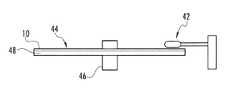
- the electronic storage device 40can include a nanocomposite article 10 including a phase separated material supported on a substrate as described herein and a read-write head 42 for reading and/or writing information to the heteroepitaxial, phase-separated layer of the nanocomposite article 10 .
- the read-write head 42can be adapted for longitudinal reading/writing.
- the read-write head 42can also be adapted for perpendicular reading/writing in order to a take advantage of the ultra high density of the ordered, magnetic nanostructures.
- the read-write head 42can be positioned to float above an upper surface 44 of the nanocomposite article 10 .
- the nanocomposite article 10can have a circular shape and can be coupled to a shaft 46 adapted to rotate the nanocomposite article 10 .
- the nanocomposite articlecan be supported by or deposited on a support 48 , e.g., a platter, which can have the same general shape as the nanocomposite article 10 .
- the read-write head 42can be adapted for moving from an inner portion of the circular nanocomposite article 10 adjacent the shaft 46 to an outer portion of the nanocomposite article 10 proximate the edge 50 .
- the read-write head 42can be communicatively coupled to a processor 52 adapted for sending and/or receiving information to and/or from an external source 54 , e.g., a central processing unit of a computer.
- the coupling between the processor 52 and the external source 54can be communicatively coupled to each other via any known wired or wireless method.
- a method of forming the nanocomposite articles 10 described hereinis also described.
- the methodcan include providing a single-crystal or single-crystal-like substrate 12 having a surface 14 ; and depositing a heteroepitaxial, phase-separated layer 16 over the surface 14 .
- the phase-separated layer 16can include a continuous, non-magnetic, crystalline, matrix phase 18 and an ordered, magnetic magnetic phase 20 disposed within the matrix phase 18 as already described herein.
- the methodcan also include forming one or more buffer layer 22 supported on the substrate 12 prior to forming the phase-separated layer 16 , which is supported on the buffer layer(s) 16 .
- the depositing stepcan include simultaneous or sequential deposition of the continuous, non-magnetic, crystalline, matrix phase 18 , and the ordered, magnetic magnetic phase 20 via an epitaxial formation technique.
- the depositing stepcan include an in-situ deposition process selected from the group consisting of pulsed laser ablation, chemical vapor deposition (CVD), metallorganic chemical vapor deposition (MOCVD), sputtering and e-beam co-evaporation.
- the depositing stepcan also include an ex-situ deposition process selected from the group consisting of chemical solution processes, and an ex-situ BaF 2 process, followed by a heat treatment.
- the depositing stepcan include a chemical solution process selected from the group consisting of TFA-MOD, non-fluorine MOD processes, and reduced fluorine MOD processes.
- the target for the epitaxial formation techniquecan include both a non-magnetic material 24 and a magnetic material 26 .
- the targetcan include 1-99 vol-% of the non-magnetic material, 25-98 vol-% of the non-magnetic material, 50-97 vol-% of the non-magnetic material, 60-96 vol-% of the non-magnetic material 24 , or any range defined by any of these end-points, e.g., 25-99 vol-% or 96-99 vol-%.
- the targetcan include 1-99 vol-% of the magnetic material, 2-75 vol-% of the magnetic material, 3-50 vol-% of the magnetic material, 4-40 vol-% of the magnetic material 26 , or any range defined by any of these end-points, e.g., 2-40 vol-% or 1-4 vol-%.
- the method for producing the phase-separated layercan involve subjecting a target material that contains two or more target components to a sputtering technique (or other deposition technique disclosed herein, e.g., pulsed laser deposition) to form a phase-separated layer supported on a substrate.
- the target materialshould include both the magnetic material and the non-magnetic material or precursors thereof.
- the deposition techniqueshould be operated under conditions appropriate for deposition of a phase-separated material that includes an ordered, magnetic magnetic phase.
- the characteristic of becoming phase-separatedcan be, for example, an inherent characteristic of the components (i.e., a propensity to phase-separate), or alternatively, a result of annealing or a reaction or interaction of the components with each other or another agent.
- the phase-separated layercan be characterized by containing regions of different compositions, or more broadly, regions having different lattice structures, i.e., regions that are crystallographically dissimilar or mismatched. Regions of different compositions will necessarily possess different lattice structures.
- the crystallographically-mismatched regions, i.e., nanostructures, in the phase-separated layerhave an ordered arrangement with respect to each other.
- the degree of order possessed by the phase-separated layeris preferably of the degree found in highly ordered self-assembled structures.
- the orderis preferably characterized by fixed or patterned distances (i.e., interspaces) between crystallographically matching regions (i.e., nanostructures) such as would be found in self-assembled (e.g., interdigitated or periodic) ordered materials.
- the distances between crystallographically matching regions, e.g., nanostructuresare constant throughout the phase-separated layer. When the distances are patterned, the distances between at least a portion of the crystallographically matching regions are different, but follow an repeating pattern throughout the phase-separated layer.
- the fixed or patterned distances between nanostructures in the phase-separated layer 14are on the nanoscale, such as a distance of about or no more than 1 nm, 2 nm, 3 nm, 4 nm, 5 nm, 10 nm, 20 nm, 30 nm, 40 nm, 50 nm, 60 nm, 70 nm, 80 nm, 90 nm, 100 nm, 150 nm, 200 nm, 250 nm, 300 nm, 350 nm, 400 nm, 450 nm, 500 nm, 550 nm, 600 nm, 650 nm, 700 nm, 750 nm, 800 nm, 850 nm, 900 nm, or 950 nm, or a distance within a particular range bounded by any two of the foregoing values.
- the fixed or patterned distances between nanostructures in the phase-separated layer 14are on the microscale, such as a distance of about or no more than 1 ⁇ m, 2 ⁇ m, 3 ⁇ m, 4 ⁇ m, 5 ⁇ m, 10 ⁇ m, 20 ⁇ m, 30 ⁇ m, 40 ⁇ m, 50 ⁇ m, 60 ⁇ m, 70 ⁇ m, 80 ⁇ m, 90 ⁇ m, 100 ⁇ m, 125 ⁇ m, 150 ⁇ m, 175 ⁇ m, 200 ⁇ m, 225 ⁇ m, or 250 ⁇ m, or a distance within a particular range bounded by any two of the foregoing values.
- a portion of the fixed or patterned distancesis within the nanoscale range while another portion of the fixed or patterned distances is within the microscale range.
- the crystallographically mismatched regions, i.e., the nanostructures, in the phase-separated layercan have any particular shape.
- at least one of the groups of phase-separated regionsare substantially spherical (e.g., globules), or coin e.g., filamentous), or plate-like.
- the columnar structurescan be, for example, a cylindrical, square, rectangular, or triangular columnar structure, or a polygonal columnar structure (e.g., pentagonal, hexagonal, or other polygonal columnar shape).
- a cylindrical columnar shapeincludes ovoid or flattened cylindrical shapes.
- the phase-separated layercan be characterized by the presence of columnar or platelike phase-separated regions having their vertical axes (i.e., length-wise or longest axes, as opposed to shorter width-wise axes) oriented non-parallel to the ordered surface of the primary substrate and/or to the surface of the phase-separated layer.
- the ends of the ordered, magnetic nanostructuresform a portion of the surface 28 of the phase-separated layer 16 , white in exemplary other materials the ordered, magnetic nanostructures are completely embedded in the non-magnetic matrix phase.
- the components in the target material 24 , 26need not be of equivalent chemical structure to the phases 18 , 20 in the phase-separated layer 16 .
- the target components 24 , 26may react with each other or the primary substrate or with a gaseous reactive component during the deposition procedure to form a new phase-separated component 24 , 26 in the phase-separated layer 16 .
- each of the target components in the target materialis necessarily present in a weight, volume, or molar percentage of less than 100% with respect to the total weight of target material.
- the percentage of one componente.g., magnetic material 26 or non-magnetic material 24
- the amount of magnetic target materialcan be represented as “A” while the amount of the non-magnetic target material can be represented as “100-A”.
- the amount of the first and second target componentscan be represented as “A” and “B”, respectively, while the amount of the third target material can be represented as “100-A-B” (and so on, for additional target components).
- the two or more target componentscan be in a mixed or separated state during the deposition process, e.g., a sputtering or pulsed laser deposition process.
- the target componentscan be mixed to any suitable degree of homogeneity.
- a mixture of target componentscan be finely mixed (e.g., variable regions can be evident only on the microscale, i.e., less than 1 micron, or nanoscale), or coarsely mixed (e.g., variable regions are evident on a size scale greater than 1, 10, 100, or 500 microns).
- the targetcan also include a disk of one material covered with a foil of the second material.
- Adjustments in the density, distribution, or size of the nanostructures in the phase-separated layercan provide a desired modulation of data storage properties. These adjustments can be achieved by judicious selection or adjustment of the conditions used in the deposition technique.
- the corresponding modulation of defects in the phase-separated layercan include, for example, an adjustment of the density distribution, interspacing, or columnar width, of or between defect features (including filaments) present in the superconducting film. Modulation of defects in the phase-separated layer can be used to form a data storage media, for example, which exhibit optimized data storage or ultra high data storage at an elevated blocking temperature (T B ).
- the “primary substrate”is the substrate upon which the phase-separated layer is deposited.
- the primary substratecan be any suitable layer that contains an ordered surface, as particularly known and used in the field of epitaxial tapes and films, e.g., superconductor or semiconductor tapes.
- the ordered surfaceis typically a result of molecular-level organization, such as found in a crystalline or polycrystalline surface.
- the primary substratecan be a biaxially-textured substrate, such as any of the biaxially-textured substrates known in the art or described herein.
- biaxially-textured substratesAny of the biaxially-textured substrates known in the art can be used as the primary substrate, e.g., buffer layer, on which the phase-separated layer is deposited.
- the term “biaxially-textured substrate” as used hereinis meant to be synonymous with the related term “sharply biaxial-textured substrate.”
- Biaxially-textured substrates suitable for use hereinis the class of rolling assisted, biaxially-textured substrates (RABiTS).
- RABiTSrolling assisted, biaxially-textured substrates
- the RABiTS methodproduces a polycrystalline substrate having primarily low angle grain boundaries. Further details of the RABiTS technique and formed substrates can be found in, for example, A. Goyal, et al., J. of Materials Research , vol. 12, pgs. 2924-2940, 1997, and D. Dimos et al., Phys. Rev. B, 41:4038-4049, 1990, the disclosures of which are incorporated herein by reference.
- the RABiTS techniqueprovides a simple method for fabricating long lengths of biaxially-textured substrates with primarily low-angle grain boundaries. These substrates have been widely employed for the epitaxial deposition of high temperature superconducting (HTS) materials.
- HTShigh temperature superconducting
- a RABiTS substratecan be prepared as follows. Briefly, a deformed metal substrate with a very well-developed copper-type (Cu-type) rolling texture is first provided.
- the metalcan be any suitable metal, and typically a FCC type of metal (e.g., Cu, Co, Mo, Cd, Pd, Pt, Ag, Al, Ni, and their alloys and more preferably, nickel and its alloys (e.g., NiW).
- a substrate with a Cu-type rolling texturecan be readily identified, as known in the art, and as disclosed in, for example, U.S. Pat. No. 7,087,113.
- a Cu-type rolling texturegenerally exhibits the characteristic that the X-ray intensity in the pole figures is concentrated on the ⁇ -fiber in Euler space of orientation representation.
- a Cu-type rolling textureis generally characterized by an orientation of all the grains in the material lying on the ⁇ -fiber.
- the ⁇ -fiberis defined as the tube or fiber running from the B through the S to the C point in Euler space.
- Cu-type rolling textureis generally best shown using pole figures of (111), (200), and (220) from the substrate or drawing the orientations in Euler Space.
- the metal with Cu-type rolling textureis annealed at a temperature higher than its secondary recrystallization temperature to provide exaggerated grain growth such that a single grain consumes other grains to form an essentially single crystalline (i.e., single grain) type of material (hereinafter, a “single crystal substrate”).
- At least one buffer layeris epitaxially deposited on the surface of the single crystal substrate.
- the function of the buffer layeris typically as a chemical barrier between the single crystal substrate and the active (e.g., phase-separated) layer, thereby preventing reaction between these layers while epitaxially transmitting the ordered crystalline structure of the single crystal substrate to the superconducting layer.
- Exemplary buffer layersinclude, but are not limited to, CeO 2 , yttria-stabilized zirconia (YSZ), (RE) 2 O 3 , wherein RE can be any rare earth metals [e.g., yttrium (Y), lanthanum (La), cerium (Ce), praseodymium (Pr), neodymium (Nd), samarium (Sm), europium (Eu), gadolinium (Gd), terbium (Tb), dysprosium (Dy), holmium (Ho), erbium (Er), thulium (Tm), ytterbium (Yb), lutetium (Lu)], LaM′O 3 , wherein M′ is a transition or main group metal (e.g., LaAlO 3 , LaGaO 3 , LaMnO 3 , LaCrO 3 , LaNiO 3 ), lanthanum zirconate (e.g.,
- RABiTS architecturesinclude, for example, a four-layer architecture, such as CeO 2 /YSZ/Y 2 O 3 /Ni/Ni—W, and a three-layer architecture, such as CeO 2 /YSZ/CeO 2 /Ni—W.
- biaxially-textured substrateincludes the ion-beam-assisted deposition (IBAD) substrate.
- IBAD processes and resulting substratesare described in, for example, U.S. Pat. Nos. 6,632,539, 6,214,772, 5,650,378, 5,872,080, 5,432,151, 6,361,598, 5,872,080, 6,756,139, 6,884,527, 6,899,928, and 6,921,741, the disclosures of which are incorporated herein by reference in their entireties.
- an IBAD substrateis characterized by an MgO layer (i.e., “IBAD-MgO”) biaxially grown using ion assist on an Al 2 O 3 /Y 2 O 3 -coated polycrystalline nickel-based alloy (generally, Hastelloy) base substrate.
- the Hastelloy substrateis typically deposited on a polycrystalline copper layer.
- the Al 2 O 3 layerserves primarily as a barrier to prevent upward diffusion of substrate components (i.e., functions as a diffusion barrier layer) while the Y 2 O 3 layer serves as a seed layer for the IBAD-MgO nucleation.
- biaxially-textured substrateincludes the inclined-substrate deposition (ISD) substrate.
- ISDinclined-substrate deposition
- the resulting substratehas rotated cube texture and the rotation can be as high as 40-45°.
- ISD processes and resulting substratesare described in, for example, U.S. Pat. Nos. 6,190,752 and 6,265,353, the disclosures of which are incorporated herein by reference in their entireties.
- a biaxially-textured layeris deposited on a flexible, polycrystalline, untextured substrate.
- the primary substrate considered hereinpossesses a textured typically, biaxially-textured) surface upon which the phase-separated layer is deposited.
- the ordered surfacecan be, for example, any of the layers described above that are typically included in a biaxially textured primary substrate, such as found in a RABiTS, IBAD, or ISD substrate.
- the surfacemay be a crystalline or polycrystalline (e.g., epitaxial) layer of a metal oxide (e.g., CeO 2 , ZrO 2 , Al 2 O 3 , Y 2 O 3 , or YSZ), metal (e.g., Ni, Cu), or metal alloy (e.g., Ni—W).
- the surfaceis a crystalline, polycrystalline, or epitaxial layer of an alkaline earth metal oxide, such as YSZ.
- the primary substrate surface on which the phase-separable components are epitaxially depositedcan influence an effect on the growth mechanisms of the phase-separated components. Accordingly, the primary substrate surface can be appropriately selected or modified in order to adjust, modulate, or optimize crystallographic and other morphological characteristics of the epitaxially-grown phase-separated layer.
- the sputtering deposition techniquecan be any of the deposition techniques known in the art in which a target material and substrate are made to assume opposite polarities within a reduced pressure atmosphere at a voltage difference sufficient to induce gas-phase sputtering of the target material, thereby resulting in the ejection of atoms of the target material and their deposition on the substrate.
- the inventionincorporates by reference all of the knowledge in the art pertaining to the concept, design, and operation of sputtering techniques useful for deposition of a film onto a substrate, as treated by, for example, K. Wasa, S.
- a sputtering processoperates by the general principle that the voltage established between the target material and substrate causes an acceleration of electrons, which, in turn, causes ionization of the gaseous medium (sputter gas) as the electrons collide with gas molecules.
- the resulting ionized gas moleculeswhich are positively charged, are made to accelerate toward the target material when the target material is held at a negative charge.
- the impact of the ionized gas molecules on the target materialcauses the ejection of atoms of the target material and their deposition onto the substrate.
- the sputtering deposition techniquecan be a direct current (DC) sputtering technique, a polarity-oscillating technique, such as a radiofrequency (RF) sputtering technique, or an ion-beam sputtering (IBS) technique.
- DCdirect current
- RFradiofrequency
- IBSion-beam sputtering
- Any of the sputtering deposition techniques contemplated hereincan, in addition, be a magnetron sputtering technique.
- a “magnetron sputtering technique”is any sputtering technique in which electrons (and resulting ions of sputter gas) are confined in a region near the target surface by a magnetic (or electromagnetic) field.
- the magnetic fieldtypically of several hundred gauss
- the magnetic fieldcan be established by, for example, placing a permanent magnet or solenoid near or within a cathode target.
- the precise magnitude of the magnetic field employeddepends to a large extent on the distance from the cathode target (sputtering gun).
- the techniqueemploys means to adjust the distance between the target 24 , 26 and substrate 12 .
- the depositionsare conducted with the substrate being about 4, 5, or 6 cm (and more preferably, about 5 cm) above the cathode target.
- Two magnetron sputtering techniques particularly considered hereinare DC magnetron sputtering and RF magnetron sputtering.
- a DC sputtering techniqueas described above, is modified by also including magnetic confinement of electrons close to the target.
- a RF sputtering techniqueas described above, is modified by also including magnetic confinement of electrons close to the target.
- the magnetron sputtering systemcan have any of the designs and arrangements known in the art, such as a cylindrical type or planar type magnetron sputtering system.
- any of the sputtering deposition techniques contemplated hereincan, in addition, be a reactive sputtering technique.
- a reactive sputtering techniquesputtered material chemically reacts with (and generally, combines with) at least some portion of the gaseous medium.
- Two reactive sputtering techniques particularly considered hereinare DC reactive sputtering and RF reactive sputtering.
- a DC sputtering techniqueas described above, is modified by also including in the gaseous medium one or more gaseous components that react with the sputtered target material.
- a RF sputtering techniqueis modified by also including in the gaseous medium one or more gaseous components that react with the sputtered target material.
- the reactive sputtering techniquecan also be a magnetron sputtering technique, such as a DC reactive magnetron sputtering technique or a RF reactive magnetron sputtering technique.
- the pulsed sputtering techniquecan be, for example, a pulsed DC sputtering technique, such as bipolar pulsed DC sputtering, or a pulsed magnetron sputtering technique, such as high power impulse magnetron sputtering (HIPIMS).
- a pulsed DC sputtering techniquesuch as bipolar pulsed DC sputtering
- a pulsed magnetron sputtering techniquesuch as high power impulse magnetron sputtering (HIPIMS).
- the sputter gasis generally composed, in at least a major proportion, of an inert gas.
- the inert gas particularly considered hereinis a noble gas, most notably argon (Ar), or alternatively, helium (He), neon (Ne), krypton (Kr), or xenon (Xe).
- Nitrogen (N 2 )can also be an inert gas when used with a target material not reactive with nitrogen.
- gasesthat may be used, either as an inert or reactive gas (depending on the conditions), include hydrogen (H 2 ), oxygen (O 2 ), carbon dioxide (CO 2 ), carbon monoxide (CO), water (H 2 O), ammonia (NH 3 ), a nitrogen oxide (e.g., NO, NO 2 , N 2 O), ozone (O 3 ), a sulfur oxide (e.g., SO 2 ), hydrogen halide (e.g., HF or HCl), or a gaseous hydrocarbon or fluorocarbon (e.g., CH 4 , CH 2 F 2 , CF 4 , C 2 H 6 , C 2 F 6 ). A combination of any two or more of these gases may also be used.
- sputter gases considered hereininclude argon-hydrogen (e.g., Ar-4% H 2 ), argon-oxygen (e.g., Ar-4% O 2 ), argon-nitrogen (e.g., Ar-10% N 2 ), argon-water, nitrogen-hydrogen, nitrogen-oxygen, nitrogen-water, CF 4 -nitrogen, CF 4 -hydrogen, CF 4 -oxygen, and CF 4 —H 2 O mixtures.
- argon-hydrogene.g., Ar-4% H 2
- argon-oxygene.g., Ar-4% O 2
- argon-nitrogene.g., Ar-10% N 2
- argon-waternitrogen-hydrogen, nitrogen-oxygen, nitrogen-water, CF 4 -nitrogen, CF 4 -hydrogen, CF 4 -oxygen, and CF 4 —H 2 O mixtures.
- water vapormay be included in minute amounts (e.g., 1-5 ⁇ 10 ⁇ 5 Torr, or a sub-range therein) in order to oxidize a sputtered target material such that the stoichiometric ratio of non-oxygen to oxygen elements is suitably adjusted or optimized.
- minute amountse.g., 1-5 ⁇ 10 ⁇ 5 Torr, or a sub-range therein
- the sputtering techniques considered hereinare generally conducted at a reduced pressure.
- the pressureis reduced to a pressure less than about 120 ⁇ 10 ⁇ 3 Torr (i.e., 120 in Torr).
- the operating pressurecan preferably be about, at least, or no more than 110, 100, 90, 80, 70, 60, 50, 40, 30, 20, 15, 12, 11, 10, 9, 8, 7, 6, 5, 4, 3, 2, 1, 0.5, 0.4, 0.3, 0.2, 0.1, 0.05, or 0.01 mTorr, or a pressure within a range bounded by any two of the foregoing exemplary values.
- a DC sputtering techniqueis practiced using an operating pressure at or above 30 mTorr.
- a RF sputtering technique or magnetron sputtering techniqueis practiced using an operating pressure below 30 mTorr.
- the sputtering techniquecan employ a suitable base pressure (i.e., background pressure of the system).
- a suitable base pressureis no more than about 5 ⁇ 10 ⁇ 5 Torr.
- the base pressurecan be about, at least, or no more than 4 ⁇ 10 ⁇ 5 Torr, 3 ⁇ 10 ⁇ 5 Torr, 2 ⁇ 10 ⁇ 5 Torr, 1 ⁇ 10 ⁇ 5 Torr, 9 ⁇ 10 ⁇ 6 Torr, 8 ⁇ 10 ⁇ 6 Torr, 7 ⁇ 10 ⁇ 6 Torr, 6 ⁇ 10 ⁇ 6 Torr, 5 ⁇ 10 ⁇ 6 Torr, 4 ⁇ 10 ⁇ 6 Torr, 3 ⁇ 10 ⁇ 6 Torr, 2 ⁇ 10 ⁇ 6 Torr, or 1 ⁇ 10 ⁇ 6 Torr, or a base pressure within a range bounded by any two of the foregoing exemplary values.
- the substrateis typically heated in order to make the deposition process more efficient.
- the temperature at which the substrate is heatedis also referred to as the “sputter temperature”.
- a sputter temperatureof at least 500° C. is employed.
- the sputter temperaturecan preferably be about, at least, or no more than 400° C., 425° C., 450° C., 475° C., 500° C., 525° C., 550° C., 575° C., 600° C., 625° C., 650° C., 675° C., 700° C., 725° C., 750° C., 775° C., 800° C., 825° C., 850° C., 875° C., or 900° C., or a sputter temperature within a range bounded by any two of the foregoing exemplary values.
- the sputter temperatureis maintained at a specific temperature, or substantially maintained at a specific temperature (i.e., within ⁇ 5° C. of a specific temperature), during the sputtering operation. In another embodiment, the sputter temperature is changed (i.e., by more than ⁇ 5° C.) during the sputtering operation. In different embodiments, the sputter temperature is increased, or decreased, or increased to a peak temperature and decreased, or decreased to abuse temperature and then increased, during the sputtering operation.
- the sputter temperatureis changed at a constant or substantially constant rate (i.e., linear or substantially linear rate), while in other embodiments, the sputter temperature is changed by a changing (i.e., non-linear) rate during the sputtering process.
- the sputtering time(i.e., time that target is being sputtered and deposited on substrate) is very much dependent, first, on the desired thickness of the film (i.e., longer sputtering times generally produce thicker films), and second, on the conditions employed (e.g., sputtering pressure, sputter temperature, sputtering power, and overall sputtering efficiency) in the sputtering technique.
- the sputtering timecan be as short as a few minutes (e.g., 1, 2, 3, 4, 5, 10, or 15 minutes), while in other embodiments, the sputtering time can be, for example, 20, 30, 40, 50, 60, 70, 80, 90, 100, 110, 120, 150, 180 minutes, or more.
- the thickness of the phase-separated layeris, generally, desirably at least 5 nm thick.
- the phase-separated layer 14can be about, at least, or no more than 5 nm, 10 nm, 15 nm, 20 nm, 25 nm, 30 nm, 40 nm, 50 nm, 60 nm, 70 nm, 80 nm, 90 nm, 100 nm, 110 nm, 120 nm, 130 nm, 140 nm, 150 nm, 160 nm, 170 nm, 180 nm, 190 nm, 200 nm, 210 nm, 220 nm, 230 nm, 240 nm, 250 nm, 260 nm, 270 nm, 280 nm, 290 nm, 300 nm, 310 nm, 320 nm, 330 nm, 340
- the sputter poweris generally at least 20 Watts (20 W). In different embodiments, the sputter power is about, at least, or no more than about 20, 30, 40, 50, 60, 70, 80, 90, 100, 110, 120, 130, 140, 150, 160, 170, 180, 190, or 200 Watts, or a power within a range bounded by any two of the foregoing values.
- the sputter power and other conditionsare preferably adjusted such that a deposition rate of at least 0.01 nm/s is attained.
- conditions of the sputtering processare adjusted such that a deposition of about or at least 0.01, 0.02, 0.03, 0.04, 0.05, 0.06, 0.07, 0.08, 0.09, 0.10, 0.11, 0.12, 0.13, 0.14, 0.15, 0.16, 0.17, 0.18, 0.19, or 0.20 nm/s is attained.
- a pre-annealing stepcan be performed on the primary substrate prior to deposition of the target material on the substrate.
- the primary substrateis placed in a closed chamber (e.g., the deposition chamber), an annealing gas (preferably, any of the inert sputtering gases described above) is introduced into the chamber, and the pressure is reduced to a suitable low pressure, such as 1, 2, or 3 mTorr, or any of the low pressures described above.
- the temperature of the primary substratecan be simultaneously or subsequently increased to a suitable annealing temperature (e.g., 700° C., 720° C., or 740° C., or any of the elevated temperatures described above for the sputter temperature).
- the temperatureis preferably increased at a set rate, such as 80° C./min., 90° C./min., 100° C./min., 110° C./min., 120° C./min., 130° C./min., 140° C./min., or 150° C./min.
- the primary substrateis preferably maintained at the annealing temperature for at least, for example, 10, 15, 30, or 45 minutes, depending on the annealing temperature and other factors.
- the primary substrateis typically cooled to a suitable cooled temperature.
- the suitable cooled temperatureis typically room temperature, which is typically a temperature within about 15-30° C., or about 25° C.
- the primary substrateis rapidly cooled (e.g., at a rate of at least 10, 15, 20, 30, 40, or 50° C./min., or within a range therein), while in other embodiments, the primary substrate is more slowly cooled (e.g., at a rate if less than 10° C./min., or about 5, 4, 3, 2, or 1° C./min., or within a range therein).
- the resulting primary substrate with deposited phase-separated layer 16can be subjected to a post-processing step.
- the post-processing stepcan function, for example, to promote, modify, adjust, or optimize a phase separation of components.
- the post-processing stepcan be a heating step, cooling step (i.e., below room temperature), pressurization, depressurization, radiation exposure step (e.g., UV, microwave, electron beam, or ion beam radiation), or a chemical exposure step (e.g., contact of the treated substrate with a vapor phase or liquid phase chemical or mixture of chemicals).
- the post-processing stepis conducted on the treated substrate while the treated substrate is at the temperature assumed upon completion of the sputtering deposition process. In another embodiment, the post-processing step is conducted on the treated substrate after it has been cooled to, for example, room temperature, and post-processed either in the cooled state or in a subsequently elevated temperature state.
- the post-processing stepcan include a heating step, such as a post-annealing step.
- the heatingmay be conducted at typical ambient pressure (e.g., 1 atm), reduced pressure (e.g., a pressure below 1 atm, or any of the reduced pressures described above), or elevated pressure (e.g., greater than 1 atm).
- the heatingcan be conducted under any suitable atmosphere, such as air, or alternatively, an artificial inert or reactive gas, such as any of the sputter gases and combinations thereof described above.
- the post-annealing temperatureis preferably any of the sputter temperatures described above (e.g., 750-800° C.).
- the post-annealing timeis dependent on several factors, including the applied temperature.
- the post-annealing timecan be any of the sputtering times given above (e.g., 15 minutes to 2 hours).
- the treated substratecan be cooled in a gradual or rapid manner, such as described above after sputtering is completed.
- a coating 30can be applied to the phase-separated layer 16 for any of a variety of purposes.
- a protective layer 30may be applied on the phase-separated layer 16 to protect the phase-separated layer 16 , such as for corrosion resistance.
- a coating 30e.g., metallic, polymeric, plastic, rubber, paint, or hybrid
- Epitaxial, self-assembled ferromagnetic cobalt nanostructures embedded in yttria-stabilized zirconia (YSZ) matrixwere grown on YSZ (001)-covered singe-crystalline Si (001) substrates by pulsed laser deposition (PLD).
- PLDpulsed laser deposition
- high quality epitaxial YSZ buffered layers of ⁇ 120 nm thicknesswere grown on Si (001) substrates using pulsed layer deposition.
- Phase-separated Co/YSZ nanocomposite filmswere then deposited on the YSZ-buffered Si (001) substrates using pulsed laser deposition (PLD).
- PLDpulsed laser deposition
- Self-assembled Co nanodots and Co nanowires embedded in YSZ matriceswere grown on the YSZ-buffered Si(001) substrates under a 4% H 2 /96% Ar atmosphere at the growth temperature 800° C. and a growth pressure of 1 mTorr.
- Laser energy density and the distance between substrate and targetwere set to 4 J/cm 2 and 6.5 cm, respectively.
- the multi-target systemwas a YSZ ceramic target (2′′ diameter) partly covered with a strip of a high-purity Co foil. The width was 0.4 cm for nanodots and 0.9 cm for nanowires. After deposition of the phase-separated layer, all samples were cooled down to room temperature at a cooling rate of 20° C./min.
- YSZwas chosen as the buffer layer to enable heteroepitaxy in both Co nanostructures and YSZ matrix.
- FIG. 3the formation of nanostructures from nanodots to nanowires was controlled by the ablation of Co and YSZ in different Co/YSZ ratios using a multi-target system of YSZ ceramic target partly covered with high-purity metallic Co stripes of different widths.
- Cross-section transmission electron microscopy (TEM) and Z-contrast scanning transmission electron microscopy (STEM) analysesconfirmed the presence of nanostructures embedded in the YSZ matrices and their varying morphology as a function of the ratio of Co and YSZ during the ablation process.
- FIG. 4( e )shows an analysis demonstrating a slight asymmetry in the shape of nanodots.
- the dimension along the growth directioni.e., c-axis
- the dimension along the growth directionis slightly larger than the orthogonal dimension. This is shown schematically in the second inset of FIG. 3( a ).
- FIG. 4( e )shows that the maximum frequency for the breadth (shortest dimension) of the nanodots is approximately 7 nm, whereas the maximum frequency for the length (longest dimension) of the nanodots is approximately 12 nm.
- the distribution of the nanodots lengthis broader than that of the breadth, which indicates that the elongated axis of the nanodots varies within a wide range along the growth direction.
- FIG. 5shows a similar analysis of the nanowires.
- the analysisshows that the average diameter and spacing for nanowires are ⁇ 7.7 nm and 28.7 nm respectively.
- the breadth of the nanodots and the diameter of the nanowireshave similar values of ⁇ 7 nm and ⁇ 7.7 nm, which confirms the increased vertical elongation during growth with increasing Co ratio. This observation demonstrates the formation pathway from nanodots nanowires that is suggested by the schematics of FIG. 3( a ).
- EDSenergy dispersive x-ray spectroscopy
- the high-resolution TEM (HRTEM) cross-section images in FIG. 6reveal the single crystal nature of the Co nanodots and nanowires embedded in the YSZ matrix.
- the images and diffraction patterns corresponding to each nanocomposite film in FIG. 6indicate a heteroepitaxial relationship between the nanodot/nanowire and the matrix.
- FIG. 4( b )shows a ⁇ -2 ⁇ scan of the epitaxial YSZ thin film grown on Si (100) before deposition of Co/YSZ nanocomposite films.
- the ⁇ -2 ⁇ scan of FIG. 4( b )exhibits only Si (n00) and YSZ (n00) peaks without any other extra peak, which is indicative of uniform orientation of deposited YSZ thin films.
- FIGS. 4( c ) and ( d )show that once the phase-separated Co/YSZ nanocomposite layer is deposited, distinct Co peaks are observed corresponding to the high degree of crystallographic orientation in the Co nanostructures.
- These Co nanostructureshave (n00)-oriented epitaxial face-centered cubic (fcc) structures with respect to YSZ matrix and Si substrates.
- a weak (111) Co peakwas detected from nanocomposite layers containing Co nanowires.
- FIG. 7shows XRD phi-scans that confirm the fcc structure of cobalt in nanodots (Sample A) and nanowires (Sample B).
- the fcc structureis evident from the four-fold symmetry, which indicates cube-on-cube epitaxial growth for Co/YSZ on YSZ buffered Si substrate.
- the free energy of hexagonal close packed (hcp) bulk cobaltis lower than that of the metastable fee phase below 700 K.
- FIG. 8( b )shows that the phase-separated material with elongated nanowires of Co exhibit magnetization loops m(H) at 100 K that show significant, orientation-dependent hysteresis.
- the loop in FIGS. 8( b )relatively “square” and has a higher coercive field when the external field H is applied parallel to the nanowires (perpendicular to the plane), which indicates that the shape anisotropy inhibits reversal of the magnetization.
- the coercive fields H care significantly higher with nanowires than with nanodots.
- FIG. 8( c )shows the hysteresis curves of Co nanowires measured at room temperature (RT, 300 K). This data was obtained with the magnetic field applied parallel and perpendicular to the plane. Compared to the low temperature measurement of nanowires in FIG. 8( b ), the magnetization loop is still relatively “square” for Co nanowires at 300 K [ FIG. 8( c )], with a lower coercive field magnetizing along the easy axis perpendiclar to plane.
- an anisotropy field of ⁇ 7000 Oersted (Oe)is obtained from the intersection of both loops along easy (out-of-plane) and hard (in-plane) axes by the magnetization measurements. This value is fairly close to the theoretical anisotropy field of ⁇ 6910 Oe for Co.
- the estimated Mscorresponds to a Co fraction of vol-2%, which is close to the value of 3.5 vol-% Co estimated from the TEM images.
- FIG. 8( d )shows the dependence of coercive fields on the temperatures for Co nanodots and nanowires embedded in YSZ matrices.
- the coercive fields of nanodots and nanowires for any field orientationdecrease as temperature increases and the coercive fields of nanowires are relatively higher than those of nanodots.
- the remarkable coercive field measurements for nanowireswere observed at 5 K for field direction perpendicular to the plane.
- Such coercive fields H creflect the size and geometry of the Co nanostructures.
- FIG. 9shows magnetic response as a function of temperature for Co nanodots and nanowires in low or zero applied magnetic fields.
- FIG. 9shows the zero-field-cooled (ZFC) and field-cooled (FC) response in 100 Oe, and out-of-plane and in-plane remanent magnetization versus temperature.
- FIG. 9( a )demonstrates that the Co nanodots exhibit a superparamagnetic response for T B > ⁇ 75 K, where T B is the blocking temperature. Above T B , magnetization becomes unstable in orientation due to thermal disorder, and the remanent magnetization is quite low.
- T Bis estimated as ⁇ 40 K for a small cylinder with a diameter of 7 nm and a length of 12 nm.
- the associated energy barrier per unit volume of particlescan be expressed with magnetocrystalline anisotropy parameters of fcc phase Co, which were taken from the experimental data.
- the experimentally observed T B of 75 Kis fairly close to the estimated T B of 40 K, with the 35 K difference within the error in the estimation of volume of nanodots for calculation of estimated T B .
- the magnetic response in Co nanowiresdepends strongly on the orientation of the external field H.
- the remanence magnetizationis large when the field is applied along the easy axis parallel to the nanowires, and much smaller when applied orthogonal to nanowires, which are aligned along the c-axis.
- the out-of-plane remanent magnetization for Co nanowiresremains large. This demonstrates usefulness of these materials for ultra-high density magnetic data storage devices.
- the zfc-fc response in a 100 Oe fieldwas very weak and no blocking temperature is observed [ FIG. 9( b )].
- Co nanowires spaced 29 nm apart embedded in an insulating YSZ matrixwill exhibit an ultrahigh magnetic recording density of at least 0.8 Tb/in 2 .
- similar resultsshould be possible by controlling the morphology of nanoparticles embedded in an insulating YSZ matrix.
Landscapes
- Engineering & Computer Science (AREA)
- Power Engineering (AREA)
- Chemical & Material Sciences (AREA)
- Inorganic Chemistry (AREA)
- Manufacturing & Machinery (AREA)
- Crystallography & Structural Chemistry (AREA)
- Biomedical Technology (AREA)
- Nanotechnology (AREA)
- Molecular Biology (AREA)
- General Health & Medical Sciences (AREA)
- Health & Medical Sciences (AREA)
- Life Sciences & Earth Sciences (AREA)
- Materials Engineering (AREA)
- Metallurgy (AREA)
- Organic Chemistry (AREA)
- Manufacturing Of Magnetic Record Carriers (AREA)
- Magnetic Record Carriers (AREA)
Abstract
Description
Claims (25)
Priority Applications (1)
| Application Number | Priority Date | Filing Date | Title |
|---|---|---|---|
| US12/956,598US8685549B2 (en) | 2010-08-04 | 2010-11-30 | Nanocomposites for ultra high density information storage, devices including the same, and methods of making the same |
Applications Claiming Priority (4)
| Application Number | Priority Date | Filing Date | Title |
|---|---|---|---|
| US12/850,398US20110034336A1 (en) | 2009-08-04 | 2010-08-04 | CRITICAL CURRENT DENSITY ENHANCEMENT VIA INCORPORATION OF NANOSCALE Ba2(Y,RE)NbO6 IN REBCO FILMS |
| US12/850,521US20110034338A1 (en) | 2009-08-04 | 2010-08-04 | CRITICAL CURRENT DENSITY ENHANCEMENT VIA INCORPORATION OF NANOSCALE Ba2(Y,RE)TaO6 IN REBCO FILMS |
| US38774310P | 2010-09-29 | 2010-09-29 | |
| US12/956,598US8685549B2 (en) | 2010-08-04 | 2010-11-30 | Nanocomposites for ultra high density information storage, devices including the same, and methods of making the same |
Related Parent Applications (1)
| Application Number | Title | Priority Date | Filing Date |
|---|---|---|---|
| US12/850,521Continuation-In-PartUS20110034338A1 (en) | 2009-08-04 | 2010-08-04 | CRITICAL CURRENT DENSITY ENHANCEMENT VIA INCORPORATION OF NANOSCALE Ba2(Y,RE)TaO6 IN REBCO FILMS |
Publications (2)
| Publication Number | Publication Date |
|---|---|
| US20120033331A1 US20120033331A1 (en) | 2012-02-09 |
| US8685549B2true US8685549B2 (en) | 2014-04-01 |
Family
ID=45556000
Family Applications (1)
| Application Number | Title | Priority Date | Filing Date |
|---|---|---|---|
| US12/956,598Active2032-01-21US8685549B2 (en) | 2010-08-04 | 2010-11-30 | Nanocomposites for ultra high density information storage, devices including the same, and methods of making the same |
Country Status (1)
| Country | Link |
|---|---|
| US (1) | US8685549B2 (en) |
Cited By (1)
| Publication number | Priority date | Publication date | Assignee | Title |
|---|---|---|---|---|
| WO2022046707A1 (en)* | 2020-08-25 | 2022-03-03 | University Of Kansas | Interfacial engineering in artificial pinning center-high temperature superconductor nanocomposites |
Families Citing this family (2)
| Publication number | Priority date | Publication date | Assignee | Title |
|---|---|---|---|---|
| KR102304722B1 (en)* | 2014-12-05 | 2021-09-27 | 삼성디스플레이 주식회사 | Organic light emitting display apparatus and method for manufacturing the same |
| CN116254508B (en)* | 2023-01-06 | 2025-03-14 | 华能国际电力股份有限公司 | Antioxidant coating for nickel-iron-based alloy surface |
Citations (77)
| Publication number | Priority date | Publication date | Assignee | Title |
|---|---|---|---|---|
| JPS6465718A (en) | 1987-09-04 | 1989-03-13 | Furukawa Electric Co Ltd | Manufacture of ceramic superconductive wire |
| US5096882A (en) | 1987-04-08 | 1992-03-17 | Hitachi, Ltd. | Process for controlling oxygen content of superconductive oxide, superconductive device and process for production thereof |
| US5164363A (en) | 1989-02-10 | 1992-11-17 | Kabushiki Kaisha Toshiba | Method for vapor-phase growth of a superconducting oxide thin film |
| US5266558A (en) | 1991-05-01 | 1993-11-30 | International Business Machines Corporation | Superconducting circuit elements with metallic substrate and method for manufacturing the same |
| US5432151A (en) | 1993-07-12 | 1995-07-11 | Regents Of The University Of California | Process for ion-assisted laser deposition of biaxially textured layer on substrate |
| US5510323A (en) | 1988-07-29 | 1996-04-23 | Hitachi, Ltd. | Tl1 (Ba1-x Sr8)2 Ca2 Cu3 Oy oxide superconductor and method of producing the same |
| EP0718897A1 (en) | 1994-12-19 | 1996-06-26 | Hitachi, Ltd. | Thallium group superconducting wire |
| US5543630A (en) | 1995-01-31 | 1996-08-06 | The United States Of America As Represented By The Secretary Of The Air Force | High Tc superconducting devices on bi-crystal substrates |
| US5650378A (en) | 1992-10-02 | 1997-07-22 | Fujikura Ltd. | Method of making polycrystalline thin film and superconducting oxide body |
| US5739086A (en) | 1995-04-10 | 1998-04-14 | Lockheed Martin Energy Systems, Inc. | Structures having enhanced biaxial texture and method of fabricating same |
| US5801105A (en) | 1995-08-04 | 1998-09-01 | Tdk Corporation | Multilayer thin film, substrate for electronic device, electronic device, and preparation of multilayer oxide thin film |
| US5846912A (en) | 1996-01-04 | 1998-12-08 | Lockheed Martin Energy Systems, Inc. | Method for preparation of textured YBa2 Cu3 Ox superconductor |
| US5872080A (en) | 1995-04-19 | 1999-02-16 | The Regents Of The University Of California | High temperature superconducting thick films |
| DE19740964A1 (en) | 1997-09-17 | 1999-03-18 | Access Ev | Substrate especially for supporting a superconductive functional layer |
| US5964966A (en) | 1997-09-19 | 1999-10-12 | Lockheed Martin Energy Research Corporation | Method of forming biaxially textured alloy substrates and devices thereon |
| US6036774A (en)* | 1996-02-26 | 2000-03-14 | President And Fellows Of Harvard College | Method of producing metal oxide nanorods |
| US6074990A (en) | 1994-12-23 | 2000-06-13 | Neocera, Inc. | Superconducting garnet thin film system |
| US6077344A (en) | 1997-09-02 | 2000-06-20 | Lockheed Martin Energy Research Corporation | Sol-gel deposition of buffer layers on biaxially textured metal substances |
| US6114287A (en) | 1998-09-30 | 2000-09-05 | Ut-Battelle, Llc | Method of deforming a biaxially textured buffer layer on a textured metallic substrate and articles therefrom |
| US6147033A (en) | 1998-09-30 | 2000-11-14 | Korea Advanced Institute Of Science And Technology | Apparatus and method for forming a film on a tape substrate |
| US6151610A (en) | 1993-12-27 | 2000-11-21 | Digital Equipment Corporation | Document display system using a scripting language having container variables setting document attributes |
| US6150034A (en) | 1998-06-12 | 2000-11-21 | Ut-Battelle, Llc | Buffer layers on rolled nickel or copper as superconductor substrates |
| US6154599A (en) | 1998-06-16 | 2000-11-28 | Christopher M. Rey | Superconducting wires fabricated using thin optical fibers |
| US6156376A (en) | 1998-06-12 | 2000-12-05 | Ut-Battelle, Llc | Buffer layers on metal surfaces having biaxial texture as superconductor substrates |
| US6180570B1 (en) | 1998-07-09 | 2001-01-30 | Ut-Battelle, Llc | Biaxially textured articles formed by plastic deformation |
| US6190752B1 (en) | 1997-11-13 | 2001-02-20 | Board Of Trustees Of The Leland Stanford Junior University | Thin films having rock-salt-like structure deposited on amorphous surfaces |
| US6214772B1 (en) | 1996-10-23 | 2001-04-10 | Fujikura Ltd. | Process for preparing polycrystalline thin film, process for preparing oxide superconductor, and apparatus therefor |
| US6231779B1 (en) | 1997-10-20 | 2001-05-15 | Massachusetts Institute Of Technology | Piezoelectric actuators and method of making same |
| US6261704B1 (en) | 1998-06-12 | 2001-07-17 | Ut-Battelle, Llc | MgO buffer layers on rolled nickel or copper as superconductor substrates |
| US6265353B1 (en) | 1996-06-05 | 2001-07-24 | Theva Duennschichttechnik Gmbh | Device and method for producing a multilayered material |
| US6270908B1 (en) | 1997-09-02 | 2001-08-07 | Ut-Battelle, Llc | Rare earth zirconium oxide buffer layers on metal substrates |
| US6331199B1 (en) | 2000-05-15 | 2001-12-18 | Ut-Battelle, Llc | Biaxially textured articles formed by powder metallurgy |
| US6361598B1 (en) | 2000-07-20 | 2002-03-26 | The University Of Chicago | Method for preparing high temperature superconductor |
| US6440211B1 (en) | 1997-09-02 | 2002-08-27 | Ut-Battelle, Llc | Method of depositing buffer layers on biaxially textured metal substrates |
| US6447714B1 (en) | 2000-05-15 | 2002-09-10 | Ut-Battelle, Llc | Method for forming biaxially textured articles by powder metallurgy |
| US6451450B1 (en) | 1995-04-10 | 2002-09-17 | Ut-Battelle, Llc | Method of depositing a protective layer over a biaxially textured alloy substrate and composition therefrom |
| US6486100B1 (en) | 1997-09-16 | 2002-11-26 | Ut-Battelle, Llc | Method for preparing preferentially oriented, high temperature superconductors using solution reagents |
| US6537689B2 (en) | 1999-11-18 | 2003-03-25 | American Superconductor Corporation | Multi-layer superconductor having buffer layer with oriented termination plane |
| US6555256B1 (en) | 1998-09-30 | 2003-04-29 | Ut-Battelle, Llc | Method of depositing an electrically conductive oxide film on a textured metallic substrate and articles formed therefrom |
| US6607313B1 (en) | 1999-06-23 | 2003-08-19 | Jds Fitel Inc. | Micro-optic delay element for use in a polarization multiplexed system |
| US6610414B2 (en) | 2001-08-16 | 2003-08-26 | Ut-Battelle, Llc | Biaxially textured articles formed by power metallurgy |
| US20030185741A1 (en) | 2001-04-06 | 2003-10-02 | Krzysztof Matyjaszewski | Process for the preparation of nanostructured materials |
| US6632539B1 (en) | 1999-11-29 | 2003-10-14 | Fujikura Ltd. | Polycrystalline thin film and method for preparing thereof, and superconducting oxide and method for preparation thereof |
| US6645313B2 (en) | 2002-02-22 | 2003-11-11 | Ut-Battelle, Llc | Powder-in-tube and thick-film methods of fabricating high temperature superconductors having enhanced biaxial texture |
| US6657229B1 (en) | 1996-05-28 | 2003-12-02 | United Microelectronics Corporation | Semiconductor device having multiple transistors sharing a common gate |
| US6670308B2 (en) | 2002-03-19 | 2003-12-30 | Ut-Battelle, Llc | Method of depositing epitaxial layers on a substrate |
| US6673646B2 (en) | 2001-02-28 | 2004-01-06 | Motorola, Inc. | Growth of compound semiconductor structures on patterned oxide films and process for fabricating same |
| US20040003768A1 (en) | 2002-07-03 | 2004-01-08 | Amit Goyal | Textured substrate tape and devices thereof |
| US6716795B2 (en) | 1999-09-27 | 2004-04-06 | Ut-Battelle, Llc | Buffer architecture for biaxially textured structures and method of fabricating same |
| US20040095658A1 (en) | 2002-09-05 | 2004-05-20 | Nanosys, Inc. | Nanocomposites |
| US6740421B1 (en) | 2003-07-14 | 2004-05-25 | Ut-Battelle, Llc | Rolling process for producing biaxially textured substrates |
| US6756139B2 (en) | 2002-03-28 | 2004-06-29 | The Regents Of The University Of California | Buffer layers on metal alloy substrates for superconducting tapes |
| US6764770B2 (en) | 2002-12-19 | 2004-07-20 | Ut-Battelle, Llc | Buffer layers and articles for electronic devices |
| US6784139B1 (en) | 2000-07-10 | 2004-08-31 | Applied Thin Films, Inc. | Conductive and robust nitride buffer layers on biaxially textured substrates |
| US6782988B2 (en) | 2001-05-16 | 2004-08-31 | L'air Liquide - Societe Anonyme A Directoire Et Consell De Surveillance Pour L'etude Et L'exploitation Des Procedes Georges Claude | Installation for the distribution and storage of cylinders of gas |
| US6867447B2 (en) | 2003-05-20 | 2005-03-15 | Texas Instruments Incorporated | Ferroelectric memory cell and methods for fabricating the same |
| US6872988B1 (en) | 2004-03-23 | 2005-03-29 | Ut-Battelle, Llc | Semiconductor films on flexible iridium substrates |
| US6884527B2 (en) | 2003-07-21 | 2005-04-26 | The Regents Of The University Of California | Biaxially textured composite substrates |
| US6899928B1 (en) | 2002-07-29 | 2005-05-31 | The Regents Of The University Of California | Dual ion beam assisted deposition of biaxially textured template layers |
| US6921741B2 (en) | 2000-12-06 | 2005-07-26 | The Regents Of The University Of California | Substrate structure for growth of highly oriented and/or epitaxial layers thereon |
| US6956012B2 (en) | 2001-06-22 | 2005-10-18 | Ut-Battelle, Llc | Method of depositing an electrically conductive oxide buffer layer on a textured substrate and articles formed therefrom |
| US20050239659A1 (en) | 2004-04-08 | 2005-10-27 | Xuming Xiong | Biaxially-textured film deposition for superconductor coated tapes |
| US20050239658A1 (en) | 2004-03-23 | 2005-10-27 | Paranthaman Mariappan P | Superconductors on iridium substrates and buffer layers |
| US6984857B2 (en) | 2003-07-16 | 2006-01-10 | Texas Instruments Incorporated | Hydrogen barrier for protecting ferroelectric capacitors in a semiconductor device and methods for fabricating the same |
| US7090785B2 (en) | 1997-10-20 | 2006-08-15 | Massachusetts Institute Of Technology | Electromechanical actuators |
| US20060234066A1 (en) | 2004-11-24 | 2006-10-19 | Zurbuchen Mark A | Topotactic anion exchange oxide films and method of producing the same |
| US20060276344A1 (en) | 2005-06-02 | 2006-12-07 | Paranthaman Mariappan P | Chemical solution deposition method of fabricating highly aligned MgO templates |
| US20070071964A1 (en)* | 2003-08-29 | 2007-03-29 | Japan Science And Technology Agency | Nano-particle device and method for manufacturing nano-particle device |
| US20070178227A1 (en) | 1999-01-12 | 2007-08-02 | Hunt Andrew T | Epitaxial thin films |
| US7323581B1 (en) | 1990-07-06 | 2008-01-29 | Advanced Technology Materials, Inc. | Source reagent compositions and method for forming metal films on a substrate by chemical vapor deposition |
| US7338907B2 (en) | 2004-10-04 | 2008-03-04 | Sharp Laboratories Of America, Inc. | Selective etching processes of silicon nitride and indium oxide thin films for FeRAM device applications |
| US7341978B2 (en) | 2005-03-04 | 2008-03-11 | Lsi Logic Corporation | Superconductor wires for back end interconnects |
| US20080176749A1 (en)* | 2005-08-01 | 2008-07-24 | Amit Goyal | High performance devices enabled by epitaxial, preferentially oriented, nanodots and/or nanorods |
| WO2008108606A1 (en) | 2007-03-08 | 2008-09-12 | Korea Advanced Institute Of Science And Technology | Apparatus for continuous fabricating superconducting tapes |
| US20090081456A1 (en) | 2007-09-26 | 2009-03-26 | Amit Goyal | Faceted ceramic fibers, tapes or ribbons and epitaxial devices therefrom |
| US20090088325A1 (en) | 2006-08-03 | 2009-04-02 | Amit Goyal | High performance electrical, magnetic, electromagnetic and electrooptical devices enabled by three dimensionally ordered nanodots and nanorods |
| US7879161B2 (en) | 2007-08-08 | 2011-02-01 | Ut-Battelle, Llc | Strong, non-magnetic, cube textured alloy substrates |
- 2010
- 2010-11-30USUS12/956,598patent/US8685549B2/enactiveActive
Patent Citations (103)
| Publication number | Priority date | Publication date | Assignee | Title |
|---|---|---|---|---|
| US5096882A (en) | 1987-04-08 | 1992-03-17 | Hitachi, Ltd. | Process for controlling oxygen content of superconductive oxide, superconductive device and process for production thereof |
| JPS6465718A (en) | 1987-09-04 | 1989-03-13 | Furukawa Electric Co Ltd | Manufacture of ceramic superconductive wire |
| US5510323A (en) | 1988-07-29 | 1996-04-23 | Hitachi, Ltd. | Tl1 (Ba1-x Sr8)2 Ca2 Cu3 Oy oxide superconductor and method of producing the same |
| US5164363A (en) | 1989-02-10 | 1992-11-17 | Kabushiki Kaisha Toshiba | Method for vapor-phase growth of a superconducting oxide thin film |
| US7323581B1 (en) | 1990-07-06 | 2008-01-29 | Advanced Technology Materials, Inc. | Source reagent compositions and method for forming metal films on a substrate by chemical vapor deposition |
| US5266558A (en) | 1991-05-01 | 1993-11-30 | International Business Machines Corporation | Superconducting circuit elements with metallic substrate and method for manufacturing the same |
| US5650378A (en) | 1992-10-02 | 1997-07-22 | Fujikura Ltd. | Method of making polycrystalline thin film and superconducting oxide body |
| US5432151A (en) | 1993-07-12 | 1995-07-11 | Regents Of The University Of California | Process for ion-assisted laser deposition of biaxially textured layer on substrate |
| US6151610A (en) | 1993-12-27 | 2000-11-21 | Digital Equipment Corporation | Document display system using a scripting language having container variables setting document attributes |
| EP0718897A1 (en) | 1994-12-19 | 1996-06-26 | Hitachi, Ltd. | Thallium group superconducting wire |
| US6074990A (en) | 1994-12-23 | 2000-06-13 | Neocera, Inc. | Superconducting garnet thin film system |
| US5543630A (en) | 1995-01-31 | 1996-08-06 | The United States Of America As Represented By The Secretary Of The Air Force | High Tc superconducting devices on bi-crystal substrates |
| US5968877A (en) | 1995-04-10 | 1999-10-19 | Lockheed Martin Energy Research Corp | High Tc YBCO superconductor deposited on biaxially textured Ni substrate |
| US5741377A (en) | 1995-04-10 | 1998-04-21 | Martin Marietta Energy Systems, Inc. | Structures having enhanced biaxial texture and method of fabricating same |
| US6235402B1 (en) | 1995-04-10 | 2001-05-22 | Ut-Battelle, Llc | Buffer layers on biaxially textured metal substrates |
| US5898020A (en) | 1995-04-10 | 1999-04-27 | Goyal; Amit | Structures having enhanced biaxial texture and method of fabricating same |
| US5958599A (en) | 1995-04-10 | 1999-09-28 | Lockheed Martin Energy Research Corporation | Structures having enhanced biaxial texture |
| US6451450B1 (en) | 1995-04-10 | 2002-09-17 | Ut-Battelle, Llc | Method of depositing a protective layer over a biaxially textured alloy substrate and composition therefrom |
| US5739086A (en) | 1995-04-10 | 1998-04-14 | Lockheed Martin Energy Systems, Inc. | Structures having enhanced biaxial texture and method of fabricating same |
| US5872080A (en) | 1995-04-19 | 1999-02-16 | The Regents Of The University Of California | High temperature superconducting thick films |
| US5801105A (en) | 1995-08-04 | 1998-09-01 | Tdk Corporation | Multilayer thin film, substrate for electronic device, electronic device, and preparation of multilayer oxide thin film |
| US5846912A (en) | 1996-01-04 | 1998-12-08 | Lockheed Martin Energy Systems, Inc. | Method for preparation of textured YBa2 Cu3 Ox superconductor |
| US6036774A (en)* | 1996-02-26 | 2000-03-14 | President And Fellows Of Harvard College | Method of producing metal oxide nanorods |
| US6657229B1 (en) | 1996-05-28 | 2003-12-02 | United Microelectronics Corporation | Semiconductor device having multiple transistors sharing a common gate |
| US6265353B1 (en) | 1996-06-05 | 2001-07-24 | Theva Duennschichttechnik Gmbh | Device and method for producing a multilayered material |
| US6214772B1 (en) | 1996-10-23 | 2001-04-10 | Fujikura Ltd. | Process for preparing polycrystalline thin film, process for preparing oxide superconductor, and apparatus therefor |
| US6077344A (en) | 1997-09-02 | 2000-06-20 | Lockheed Martin Energy Research Corporation | Sol-gel deposition of buffer layers on biaxially textured metal substances |
| US6440211B1 (en) | 1997-09-02 | 2002-08-27 | Ut-Battelle, Llc | Method of depositing buffer layers on biaxially textured metal substrates |
| US6399154B1 (en) | 1997-09-02 | 2002-06-04 | Ut-Battelle, Llc | Laminate article |
| US6663976B2 (en) | 1997-09-02 | 2003-12-16 | Ut-Battelle, Llc | Laminate articles on biaxially textured metal substrates |
| US6270908B1 (en) | 1997-09-02 | 2001-08-07 | Ut-Battelle, Llc | Rare earth zirconium oxide buffer layers on metal substrates |
| US6486100B1 (en) | 1997-09-16 | 2002-11-26 | Ut-Battelle, Llc | Method for preparing preferentially oriented, high temperature superconductors using solution reagents |
| DE19740964A1 (en) | 1997-09-17 | 1999-03-18 | Access Ev | Substrate especially for supporting a superconductive functional layer |
| US5964966A (en) | 1997-09-19 | 1999-10-12 | Lockheed Martin Energy Research Corporation | Method of forming biaxially textured alloy substrates and devices thereon |
| US6106615A (en) | 1997-09-19 | 2000-08-22 | Goyal; Amit | Method of forming biaxially textured alloy substrates and devices thereon |
| US7090785B2 (en) | 1997-10-20 | 2006-08-15 | Massachusetts Institute Of Technology | Electromechanical actuators |
| US6231779B1 (en) | 1997-10-20 | 2001-05-15 | Massachusetts Institute Of Technology | Piezoelectric actuators and method of making same |
| US6190752B1 (en) | 1997-11-13 | 2001-02-20 | Board Of Trustees Of The Leland Stanford Junior University | Thin films having rock-salt-like structure deposited on amorphous surfaces |
| US6150034A (en) | 1998-06-12 | 2000-11-21 | Ut-Battelle, Llc | Buffer layers on rolled nickel or copper as superconductor substrates |
| US6156376A (en) | 1998-06-12 | 2000-12-05 | Ut-Battelle, Llc | Buffer layers on metal surfaces having biaxial texture as superconductor substrates |
| US6261704B1 (en) | 1998-06-12 | 2001-07-17 | Ut-Battelle, Llc | MgO buffer layers on rolled nickel or copper as superconductor substrates |
| US6468591B1 (en) | 1998-06-12 | 2002-10-22 | Ut-Battelle, Llc | Method for making MgO buffer layers on rolled nickel or copper as superconductor substrates |
| US6159610A (en) | 1998-06-12 | 2000-12-12 | Ut-Battelle, Llc | Buffer layers on metal surfaces having biaxial texture as superconductor substrates |
| US6154599A (en) | 1998-06-16 | 2000-11-28 | Christopher M. Rey | Superconducting wires fabricated using thin optical fibers |
| US6180570B1 (en) | 1998-07-09 | 2001-01-30 | Ut-Battelle, Llc | Biaxially textured articles formed by plastic deformation |
| US6375768B1 (en) | 1998-07-09 | 2002-04-23 | Ut-Battelle, Llc | Method for making biaxially textured articles by plastic deformation |
| US6555256B1 (en) | 1998-09-30 | 2003-04-29 | Ut-Battelle, Llc | Method of depositing an electrically conductive oxide film on a textured metallic substrate and articles formed therefrom |
| US6147033A (en) | 1998-09-30 | 2000-11-14 | Korea Advanced Institute Of Science And Technology | Apparatus and method for forming a film on a tape substrate |
| US6114287A (en) | 1998-09-30 | 2000-09-05 | Ut-Battelle, Llc | Method of deforming a biaxially textured buffer layer on a textured metallic substrate and articles therefrom |
| US20070178227A1 (en) | 1999-01-12 | 2007-08-02 | Hunt Andrew T | Epitaxial thin films |
| US6607313B1 (en) | 1999-06-23 | 2003-08-19 | Jds Fitel Inc. | Micro-optic delay element for use in a polarization multiplexed system |
| US6716795B2 (en) | 1999-09-27 | 2004-04-06 | Ut-Battelle, Llc | Buffer architecture for biaxially textured structures and method of fabricating same |
| US6537689B2 (en) | 1999-11-18 | 2003-03-25 | American Superconductor Corporation | Multi-layer superconductor having buffer layer with oriented termination plane |
| US6632539B1 (en) | 1999-11-29 | 2003-10-14 | Fujikura Ltd. | Polycrystalline thin film and method for preparing thereof, and superconducting oxide and method for preparation thereof |
| US6602313B2 (en) | 2000-05-15 | 2003-08-05 | Ut Battelle, Llc | Biaxially textured articles formed by powder metallurgy |
| US6599346B2 (en) | 2000-05-15 | 2003-07-29 | Ut-Battelle, Llc | Biaxially textured articles formed by powder metallurgy |
| US6846344B2 (en) | 2000-05-15 | 2005-01-25 | Ut-Battelle, Llc | Biaxially textured articles formed by powder metallurgy |
| US6610413B2 (en) | 2000-05-15 | 2003-08-26 | Ut-Battelle, Llc | Biaxially textured articles formed by powder metallurgy |
| US6635097B2 (en) | 2000-05-15 | 2003-10-21 | Ut-Battelle, Llc | Biaxially textured articles formed by powder metallurgy |
| US6797030B2 (en) | 2000-05-15 | 2004-09-28 | Ut-Battelle, Llc | Biaxially textured articles formed by powder metallurgy |
| US6607838B2 (en) | 2000-05-15 | 2003-08-19 | Amit Goyal | Biaxially textured articles formed by powder metallurgy |
| US6607839B2 (en) | 2000-05-15 | 2003-08-19 | Ut-Battelle, Llc | Biaxially textured articles formed by powder metallurgy |
| US6447714B1 (en) | 2000-05-15 | 2002-09-10 | Ut-Battelle, Llc | Method for forming biaxially textured articles by powder metallurgy |
| US6790253B2 (en) | 2000-05-15 | 2004-09-14 | Ut-Battelle, Llc | Biaxially textured articles formed by powder metallurgy |
| US6890369B2 (en) | 2000-05-15 | 2005-05-10 | Ut-Battelle, Llc | Biaxially textured articles formed by powder metallurgy |
| US6331199B1 (en) | 2000-05-15 | 2001-12-18 | Ut-Battelle, Llc | Biaxially textured articles formed by powder metallurgy |
| US6902600B2 (en) | 2000-05-15 | 2005-06-07 | Ut-Battelle, Llc | Biaxially textured articles formed by powder metallurgy |
| US6784139B1 (en) | 2000-07-10 | 2004-08-31 | Applied Thin Films, Inc. | Conductive and robust nitride buffer layers on biaxially textured substrates |
| US6361598B1 (en) | 2000-07-20 | 2002-03-26 | The University Of Chicago | Method for preparing high temperature superconductor |
| US6921741B2 (en) | 2000-12-06 | 2005-07-26 | The Regents Of The University Of California | Substrate structure for growth of highly oriented and/or epitaxial layers thereon |
| US6673646B2 (en) | 2001-02-28 | 2004-01-06 | Motorola, Inc. | Growth of compound semiconductor structures on patterned oxide films and process for fabricating same |
| US20030185741A1 (en) | 2001-04-06 | 2003-10-02 | Krzysztof Matyjaszewski | Process for the preparation of nanostructured materials |
| US6782988B2 (en) | 2001-05-16 | 2004-08-31 | L'air Liquide - Societe Anonyme A Directoire Et Consell De Surveillance Pour L'etude Et L'exploitation Des Procedes Georges Claude | Installation for the distribution and storage of cylinders of gas |
| US6956012B2 (en) | 2001-06-22 | 2005-10-18 | Ut-Battelle, Llc | Method of depositing an electrically conductive oxide buffer layer on a textured substrate and articles formed therefrom |
| US6610414B2 (en) | 2001-08-16 | 2003-08-26 | Ut-Battelle, Llc | Biaxially textured articles formed by power metallurgy |
| US6645313B2 (en) | 2002-02-22 | 2003-11-11 | Ut-Battelle, Llc | Powder-in-tube and thick-film methods of fabricating high temperature superconductors having enhanced biaxial texture |
| US6670308B2 (en) | 2002-03-19 | 2003-12-30 | Ut-Battelle, Llc | Method of depositing epitaxial layers on a substrate |
| US6756139B2 (en) | 2002-03-28 | 2004-06-29 | The Regents Of The University Of California | Buffer layers on metal alloy substrates for superconducting tapes |
| US20040003768A1 (en) | 2002-07-03 | 2004-01-08 | Amit Goyal | Textured substrate tape and devices thereof |
| US7087113B2 (en) | 2002-07-03 | 2006-08-08 | Ut-Battelle, Llc | Textured substrate tape and devices thereof |
| US6899928B1 (en) | 2002-07-29 | 2005-05-31 | The Regents Of The University Of California | Dual ion beam assisted deposition of biaxially textured template layers |
| US20040095658A1 (en) | 2002-09-05 | 2004-05-20 | Nanosys, Inc. | Nanocomposites |
| US6764770B2 (en) | 2002-12-19 | 2004-07-20 | Ut-Battelle, Llc | Buffer layers and articles for electronic devices |
| US6867447B2 (en) | 2003-05-20 | 2005-03-15 | Texas Instruments Incorporated | Ferroelectric memory cell and methods for fabricating the same |
| US6740421B1 (en) | 2003-07-14 | 2004-05-25 | Ut-Battelle, Llc | Rolling process for producing biaxially textured substrates |
| US6984857B2 (en) | 2003-07-16 | 2006-01-10 | Texas Instruments Incorporated | Hydrogen barrier for protecting ferroelectric capacitors in a semiconductor device and methods for fabricating the same |
| US6884527B2 (en) | 2003-07-21 | 2005-04-26 | The Regents Of The University Of California | Biaxially textured composite substrates |
| US20070071964A1 (en)* | 2003-08-29 | 2007-03-29 | Japan Science And Technology Agency | Nano-particle device and method for manufacturing nano-particle device |
| US20050239658A1 (en) | 2004-03-23 | 2005-10-27 | Paranthaman Mariappan P | Superconductors on iridium substrates and buffer layers |
| US6872988B1 (en) | 2004-03-23 | 2005-03-29 | Ut-Battelle, Llc | Semiconductor films on flexible iridium substrates |
| US20050239659A1 (en) | 2004-04-08 | 2005-10-27 | Xuming Xiong | Biaxially-textured film deposition for superconductor coated tapes |
| US7338907B2 (en) | 2004-10-04 | 2008-03-04 | Sharp Laboratories Of America, Inc. | Selective etching processes of silicon nitride and indium oxide thin films for FeRAM device applications |
| US20080241581A1 (en) | 2004-11-24 | 2008-10-02 | Zurbuchen Mark A | Epitaxial Layer Structures and Precursors for Topotactic Anion Exchange Oxide Films |
| US20060234066A1 (en) | 2004-11-24 | 2006-10-19 | Zurbuchen Mark A | Topotactic anion exchange oxide films and method of producing the same |
| US7208044B2 (en) | 2004-11-24 | 2007-04-24 | Mark A. Zurbuchen | Topotactic anion exchange oxide films and method of producing the same |
| US7341978B2 (en) | 2005-03-04 | 2008-03-11 | Lsi Logic Corporation | Superconductor wires for back end interconnects |
| US20060276344A1 (en) | 2005-06-02 | 2006-12-07 | Paranthaman Mariappan P | Chemical solution deposition method of fabricating highly aligned MgO templates |
| US7553799B2 (en) | 2005-06-02 | 2009-06-30 | Ut-Battelle, Llc | Chemical solution deposition method of fabricating highly aligned MgO templates |
| US20080176749A1 (en)* | 2005-08-01 | 2008-07-24 | Amit Goyal | High performance devices enabled by epitaxial, preferentially oriented, nanodots and/or nanorods |
| US20090088325A1 (en) | 2006-08-03 | 2009-04-02 | Amit Goyal | High performance electrical, magnetic, electromagnetic and electrooptical devices enabled by three dimensionally ordered nanodots and nanorods |
| WO2008108606A1 (en) | 2007-03-08 | 2008-09-12 | Korea Advanced Institute Of Science And Technology | Apparatus for continuous fabricating superconducting tapes |
| US7879161B2 (en) | 2007-08-08 | 2011-02-01 | Ut-Battelle, Llc | Strong, non-magnetic, cube textured alloy substrates |
| US20090081456A1 (en) | 2007-09-26 | 2009-03-26 | Amit Goyal | Faceted ceramic fibers, tapes or ribbons and epitaxial devices therefrom |
Non-Patent Citations (46)
| Title |
|---|
| Ahn et al., "Heterogeneous Three-Dimensional Electronics by Use of Printed Semiconductor Nanomaterials," Science vol. 314, (2006) pp. 1754-1757. |
| Aytug et al., "Enhanced flux pinning in MOCVD-YBCO films through Zr additions: systematic feasibility studies," Superconductor Science and Technology, vol. 23, (2010), pp. 1-7. |
| Aytug et al., "Enhancement of Flux Pinning in YBa2Cu3O7-8 Films via Nano-Scale Modifications of Substrate Surfaces," Oak Ridge National Laboratory, Oak Ridge, TN 37831, ISBN: 978-1-60021-692-3, pp. 237-262, 2007. |
| Aytug et al., "ORNL-Superpower CRADA: Development of MOCVD-based IBAD-2G wires" 2008, Retrieved from URL: http://111.htspeereview.com/2008/pdfs/presentations/wednesday/2G/5-2g-ornl-superpower. pdf [retrieved on Oct. 21, 2010]. |
| Aytug, "Deposition studies and coordinated characterization of MOCVD YBCO films on IBAD-MgO templates," Superconductor Science and Technology, vol. 22, (2009) p. 1. |
| Chen et al., "Metal Organic Chemical Vapor Deposition for the Fabrication of YBCO Superconducting Tapes," SuperPower Inc., Schenectady, NY 12304, ISBN: 978-1-60021-692-1, pp. 205-216, 2007. |
| Comini et al., "Quasi-one dimensional metal oxide semiconductors; Preparation, characterization and application as chemical sensors," Progress in Materials Science, vol. 54, No. 1 (2009) pp. 1-67. |
| Das et al., Novel nonlithographic quantum wire array fabrication: Physica E-Low-Dimensional Systems and Nanostructures, Elsevier Science BV, NL LNKD-DOI:10.1016/J.Physe.2005. 10.015, vol. 36, No. 2, 3 (2007), pp. 133-139. |
| Duan et al., "Indium phosphide nanowires as building blocks for nanoscale electronic and optoelectronic devices," Optoelectronic Devices, Nature, vol. 409, (2001) pp. 66-69. |
| Gao, et al., Single and Binary Rare Earth REBa2Cu3O7-8 Thin Films Prepared by Chemical Solution Deposition, J. Phys. Conf. Series, vol. 97, (2008) pp. 1-5. |
| Goyal et al., "Irradiation-free, columnar defects comprised of self-assembled nanodots and nanorods resulting in strongly enhanced flux-pinning in YBa2Cu3O7-8 films," Superconductor Science and Technology, vol. 18, No. 11, (2005) pp. 1533-1538. |
| Goyal et al., "Self-assembled, ferromagnetic Co/YSZ nanocomposite films for ultrahigh density storage media," Abstract Submitted, Dec. 9, 2009. |
| Han et al., "Transition Metal Oxide Core-Shell Nanowires: Generic Synthesis and Transport Studies," Nano Letters, vol. 4, No. 7, (2004) pp. 1241-1246. |
| Harrington et al., "Self-assembled, rare earth tantalite pyrochlore nanoparticles for superior flux pinning in YBa2Cu3O7-8 films," Superconductor Science and Technology, Issue 2 (2009), pp. 1-5. |
| Haugan et al., "In-Situ Approach to Introduce Flux Pinning in YBCO," Air Force Research Laboratory, ISBN: 978-1-60021-692-3, pp. 59-77, 2007. |
| Hikichi et al., "Property and Structure of YBa2Cu3O7-x-Nb2O5 Composite," Journal of Applied Physics, vol. 31, (1992) L1234, col. 2 Paragraph 1. |
| Huang et al., "Room-Temperature Ultraviolet Nanowire Nanolasers," Science, vol. 292, (2001) pp. 1897-1899. |
| Javey et al., "Layer-by-Layer Assembly of Nanowires fore Three-Dimensional, Multifunctional Electronics," Nano Letters, vol. 7, No. 3 (2007) pp. 773-777. |
| Kang et al., "High-Performance High-Tc Superconducting Wires," Science, DOI:10.1126/Science.1124872, vol. 331, No. 31 (2006), pp. 1911-SOM. |
| Kang et al., "Supporting material: High-performance H-Tc Superconducting Wires," Science, vol. 331 (2006) 2 pp., col. 1, paragraph 3. |
| Kar et al., "Synthesis and Characterization of One-dimensional MgO Nanostructures," J. Nanosci. Nanotech, vol. 314, (2006) pp. 1447-1452. |
| Kita et al., "Effect of Ta2O5 addition on the superconducting properties of REBa2CU3Ogamma," Physica C: vol. 445-448, (2006) pp. 391-394. |
| Kita et al., "Effect of Ta2O5 addition on the superconducting properties of REBa2CU3Oγ," Physica C: vol. 445-448, (2006) pp. 391-394. |
| Kuchibhatla et al., "One dimensional nanostructured materials," Progress in Materials Science, Pergamon Press, GB-LNKD DOI: 10.1016/J.Pmatsci.2006.08.001, vol. 52, No. 5 (2007) pp. 699-913. |
| Le et al., Systematic studies of the epitaxial growth of single-crystal ZnO nanorods on GaN using hydrothermal synthesis,: Journal of Crystal Growth, Elsevier, Amsterdam, NL LNKD-DOI:10.1016/J.Jcrysgro.2006.04.082, vol. 293, No. 1 (2006) pp. 36-42. |
| Lei et al., "Highly ordered nanostructures with tunable size, shape and properties: A new way to surface non-pattering using ultra-thin alumina masks," Progress in Materials Science, Pergamon Press, GB LNKD-DOI: 10.1016/J.Pmatsci.2006.07.002, vol. 52, No. 4 (2007) pp. 465-539. |
| Liang et al., "Preparation of Free-Standing Nanowire Arrays on Conductive Substrates," J. Am. Chem. Soc. vol. 126 (2004) pp. 16338-16339. |
| Lu et al., "Quasi-one-dimensional metal oxide materials-Synthesis, properties and applications," Materials Science and Engineering R: Reports, Elsevier Sequoia S.A., Lausanne, CH LNKD-DOI:10.1016/J.Mser.2006.04.002, vol. 52, No. 103, (2006) pp. 49-91. |
| Ma et al., "Growth and properties of YBCO-coated conductors fabricated by inclined-substrate deposition," IEE Transactions on Applied Superconductivity, vol. 15, No. 2 (2005) pp. 2970-2973. |
| McIntyre et al., "Metalorganic deposition of high-JcBa2YCu3O7-x thin films from trifluoroacetate precursors onto (100) SrTiO3," Journal of Applied Physics, vol. 68, No. 8 (1990) pp. 4183-4187. |
| Morales et al. "A laser Ablation Method for the Synthesis of Crystalline Semiconductor Nanowires," Science, vol. 279 (1998) pp. 208-211. |
| Nagashima et al., "Epitaxial Growth of MgO Nanowires by Pulsed Laser Deposition," J. Appl. Phys., vol. 101 (2007) pp. 124304-1 to 124304-4. |
| Pan et al., "Nanobelts of Semiconducting Oxides," Science, vol. 291, (2001) pp. 1947-1949. |
| Paranthaman et al., "Flux Pinning and AC Loss in Second Generation High Temperature Superconductor Wires," Oak Ridge National Laboratory, Oak Ridge, TN 37832, ISBN: 978-1-60021-692-3, pp. 3-10, 2007. |
| Pomar et al., "Enhanced vortex pinning in YBCO coated conductors with BZO nanoparticles from chemical solution deposition," IEEE Transactions on Applied Superconductivity, vol. 19, No. 3, (2009) pp. 3258-3261. |
| Saylor et al., "Experimental Method for Determining surface Energy Anisotropy and its Application to Magnesia," Journal of the American Ceramic Society, vol. 83, No. 5, (2004) pp. 1226-1232. |
| Selvamanickam et al., "High-current Y-Ba-Cu-O coated conductor using metal organic chemical-vapor Deposition, and ion-beam-assisted deposition," IEEE Transactions on Applied Superconductivity, vol. 11, No. 1 (2001) pp. 3379-3381. |
| Shin et al, "Epitaxial, Ferromagnetic, Co Nanostructures within Insulating YSZ (100) Thin Films via Pulsed Layer Deposition on Si (100)," Symposium on Mukltifunctional Oxide, Materials Science & Technology Meeting, Oct. 25-29, 2009; Abstract.* |
| Su et al., "Fabrication of thin films of multi-oxides (YBa2Cu3O7-8) starting from nanoparticles of mixed ions," Superconductor Science and Technology, vol. 19, No. 11, (2006) pp. L51-L54. |
| Wang et al., "Growth of Nanowires," Mater. Sci. & Eng., vol. 60, No. 1-6 (2008) pp. 1-51. |
| Wee et al., "Enhanced flux pinning and critical current density via incorporation of self-assembled rare-earth barium tantalite nanocolumns with YBa2Cu3O7-8 films," Physical Review B., vol. 81, No. 14 (2010) pp. 140503/1-14053/2. |
| Wee et al., "Formation of Self-Assembled, Double Perovskite, Ba2YNbO6 Nanocolumns and Their Contribution to Flux-Pinning and Jc in Nb-Doped YBa2Cu3O7-8 Films," Applied Physics Express, vol. 3, Issue 2, (2010) pp. 023101-023101-3. |
| Wee et al., "High Performance Superconducting Wire in High Applied Magnetic Fields via Nanoscale Defect Engineering," Superconductor Science and Technology, (2008) pp. 1-4. |
| Yamada et al., "Towards the practical PLD-IBAD coated conductor fabrication-Long wire, high production rate and Jc enhancement in a magnetic field," Physica C: vol. 445-448 (2006) pp. 504-508. |
| Yamada et al., Reel-to-Reel Pulsed Laser Deposition of YBCO Thick Films, Nagoya Coated Conductor Center, Superconductivity Research Laboratory, ISTEC, 2-4-1, Mutsuno, Atsuta-ku, Nagoya, 456,-8587-Japan, ISBN 978-1-60021-692-3, pp. 95-119, 2007. |
| Yoo et al., "Electrocatalytic application of a vertical Au nanorod array using ultrathin Pt/Ru/Pt layer-by-layer coatings," Electrochimica ACTA, vol. 53, No. 1-3 (2007) pp. 3656-3662. |
Cited By (1)
| Publication number | Priority date | Publication date | Assignee | Title |
|---|---|---|---|---|
| WO2022046707A1 (en)* | 2020-08-25 | 2022-03-03 | University Of Kansas | Interfacial engineering in artificial pinning center-high temperature superconductor nanocomposites |
Also Published As
| Publication number | Publication date |
|---|---|
| US20120033331A1 (en) | 2012-02-09 |
Similar Documents
| Publication | Publication Date | Title |
|---|---|---|
| US8034745B2 (en) | High performance devices enabled by epitaxial, preferentially oriented, nanodots and/or nanorods | |
| US8119571B2 (en) | High performance electrical, magnetic, electromagnetic and electrooptical devices enabled by three dimensionally ordered nanodots and nanorods | |
| Li et al. | Fabrication of ultrathin epitaxial γ-Fe2O3 films by reactive sputtering | |
| Nogués et al. | Exchange bias in ferromagnetic nanoparticles embedded in an antiferromagnetic matrix | |
| US8486864B2 (en) | Method for producing microstructured templates and their use in providing pinning enhancements in superconducting films deposited thereon | |
| JP6647590B2 (en) | Perpendicular magnetic film, perpendicular magnetic film structure, magnetoresistive element and perpendicular magnetic recording medium | |
| Katiyar et al. | Magnetic properties of self-assembled nanoscale La 2/3 Ca 1/3 MnO 3 particles in an alumina matrix | |
| US8685549B2 (en) | Nanocomposites for ultra high density information storage, devices including the same, and methods of making the same | |
| JP2003008090A (en) | Superconducting thin film having columnar pinning center using nanodots and method of manufacturing the same | |
| Dwivedi et al. | Pulsed laser deposited ferromagnetic chromium dioxide thin films for applications in spintronics | |
| US7902119B2 (en) | Porous ceramic high temperature superconductors and method of making same | |
| Martinez et al. | Study of the properties of iron oxide nanostructures | |
| Zurauskiene et al. | Nanostructured La–Sr–Mn–Co–O films for room-temperature pulsed magnetic field sensors | |
| Khurshid et al. | Microstructural and magnetic properties of CoPt nanowires | |
| Rakshit et al. | Correlations between morphology, crystal structure, and magnetization of epitaxial cobalt-platinum films grown with pulsed laser ablation | |
| GB2468924A (en) | High temperature superconductors | |
| Butera et al. | Shift in the magnetic percolation threshold of phase separated Co-rich CoAg very thin films due to reduced dimensionality | |
| Antony et al. | Ferromagnetism in Ti-doped ZnO nanoclusters above room temperature | |
| Su et al. | Chemical synthesis and magnetic properties of well-coupled FePt/Fe compositenanotubes | |
| Narayan et al. | Novel methods of forming self-assembled nanostructured materials: Ni nanodots in Al2O3 and TiN matrices | |
| Parvin et al. | Epitaxial L1 0-MnAl Thin Films with High Perpendicular Magnetic Anisotropy and Small Surface Roughness | |
| Ning et al. | Exchange Bias Effect and Magnetic Properties in ${\hbox {La}} _ {0.7}{\hbox {Sr}} _ {0.3}{\hbox {MnO}} _ {3}\hbox {-}{\hbox {NiO}} $ Nanocomposite Films | |
| Trukhanov et al. | Magnetic and electrotransport properties of the anion-deficient manganites with perovskite structure | |
| Kumar et al. | Improved magnetic properties of self-assembled epitaxial nickel nanocrystallites in thin-film ceramic matrix | |
| Saravanan et al. | Tailoring the structural and magnetic properties of sol-gel derived Sm–Co nanogranular films |
Legal Events
| Date | Code | Title | Description |
|---|---|---|---|
| FEPP | Fee payment procedure | Free format text:PAYOR NUMBER ASSIGNED (ORIGINAL EVENT CODE: ASPN); ENTITY STATUS OF PATENT OWNER: SMALL ENTITY | |
| AS | Assignment | Owner name:UT-BATTELLE, LLC, TENNESSEE Free format text:ASSIGNMENT OF ASSIGNORS INTEREST;ASSIGNOR:OAK RIDGE ASSOCIATED UNIVERSITIES;REEL/FRAME:031711/0960 Effective date:20131120 Owner name:OAK RIDGE ASSOCIATED UNIVERSITIES, TENNESSEE Free format text:ASSIGNMENT OF ASSIGNORS INTEREST;ASSIGNOR:SHIN, JUNSOO;REEL/FRAME:031711/0928 Effective date:20131115 Owner name:UT-BATTELLE, LLC, TENNESSEE Free format text:ASSIGNMENT OF ASSIGNORS INTEREST;ASSIGNOR:GOYAL, AMIT;REEL/FRAME:031711/0776 Effective date:20131122 | |
| AS | Assignment | Owner name:U.S. DEPARTMENT OF ENERGY, DISTRICT OF COLUMBIA Free format text:CONFIRMATORY LICENSE;ASSIGNOR:UT-BATTELLE, LLC;REEL/FRAME:031796/0341 Effective date:20130115 | |
| STCF | Information on status: patent grant | Free format text:PATENTED CASE | |
| MAFP | Maintenance fee payment | Free format text:PAYMENT OF MAINTENANCE FEE, 4TH YR, SMALL ENTITY (ORIGINAL EVENT CODE: M2551) Year of fee payment:4 | |
| MAFP | Maintenance fee payment | Free format text:PAYMENT OF MAINTENANCE FEE, 8TH YR, SMALL ENTITY (ORIGINAL EVENT CODE: M2552); ENTITY STATUS OF PATENT OWNER: SMALL ENTITY Year of fee payment:8 |