US8683221B2 - Configurable memory encryption with constant pipeline delay in a multi-core processor - Google Patents
Configurable memory encryption with constant pipeline delay in a multi-core processorDownload PDFInfo
- Publication number
- US8683221B2 US8683221B2US13/274,726US201113274726AUS8683221B2US 8683221 B2US8683221 B2US 8683221B2US 201113274726 AUS201113274726 AUS 201113274726AUS 8683221 B2US8683221 B2US 8683221B2
- Authority
- US
- United States
- Prior art keywords
- data
- processor
- encrypted
- data transfer
- pipeline
- Prior art date
- Legal status (The legal status is an assumption and is not a legal conclusion. Google has not performed a legal analysis and makes no representation as to the accuracy of the status listed.)
- Expired - Fee Related, expires
Links
Images


Classifications
- G—PHYSICS
- G06—COMPUTING OR CALCULATING; COUNTING
- G06F—ELECTRIC DIGITAL DATA PROCESSING
- G06F15/00—Digital computers in general; Data processing equipment in general
- G06F15/16—Combinations of two or more digital computers each having at least an arithmetic unit, a program unit and a register, e.g. for a simultaneous processing of several programs
- G06F15/163—Interprocessor communication
- G06F15/167—Interprocessor communication using a common memory, e.g. mailbox
- H—ELECTRICITY
- H04—ELECTRIC COMMUNICATION TECHNIQUE
- H04L—TRANSMISSION OF DIGITAL INFORMATION, e.g. TELEGRAPHIC COMMUNICATION
- H04L49/00—Packet switching elements
- H04L49/10—Packet switching elements characterised by the switching fabric construction
- H04L49/101—Packet switching elements characterised by the switching fabric construction using crossbar or matrix
- H—ELECTRICITY
- H04—ELECTRIC COMMUNICATION TECHNIQUE
- H04L—TRANSMISSION OF DIGITAL INFORMATION, e.g. TELEGRAPHIC COMMUNICATION
- H04L49/00—Packet switching elements
- H04L49/10—Packet switching elements characterised by the switching fabric construction
- H04L49/109—Integrated on microchip, e.g. switch-on-chip
- H—ELECTRICITY
- H04—ELECTRIC COMMUNICATION TECHNIQUE
- H04L—TRANSMISSION OF DIGITAL INFORMATION, e.g. TELEGRAPHIC COMMUNICATION
- H04L49/00—Packet switching elements
- H04L49/50—Overload detection or protection within a single switching element
- H04L49/505—Corrective measures
- H04L49/506—Backpressure
- H—ELECTRICITY
- H04—ELECTRIC COMMUNICATION TECHNIQUE
- H04L—TRANSMISSION OF DIGITAL INFORMATION, e.g. TELEGRAPHIC COMMUNICATION
- H04L49/00—Packet switching elements
- H04L49/55—Prevention, detection or correction of errors
- H04L49/555—Error detection
- H—ELECTRICITY
- H04—ELECTRIC COMMUNICATION TECHNIQUE
- H04L—TRANSMISSION OF DIGITAL INFORMATION, e.g. TELEGRAPHIC COMMUNICATION
- H04L49/00—Packet switching elements
- H04L49/15—Interconnection of switching modules
- H04L49/1515—Non-blocking multistage, e.g. Clos
- H04L49/1546—Non-blocking multistage, e.g. Clos using pipelined operation
Definitions
- the present inventionrelates to communication systems, in particular, to operations for testing encryption and decryption datapaths of an accelerated processor architecture for packet networks.
- Network processorsare generally used for analyzing and processing packet data for routing and switching packets in a variety of applications, such as network surveillance, video transmission, protocol conversion, voice processing, and internet traffic routing.
- Early types of network processorswere based on software-based approaches with general-purpose processors, either singly or in a multi-core implementation, but such software-based approaches are slow. Further, increasing the number of general-purpose processors diminished performance improvements, or actually slowed down overall network processor throughput.
- Newer designsadd hardware accelerators to offload certain tasks from the general-purpose processors, such as encryption/decryption, packet data inspections, and the like. These newer network processor designs are traditionally implemented with either i) a non-pipelined architecture or ii) a fixed-pipeline architecture.
- non-pipelined architecturegeneral-purpose processors are responsible for each action taken by acceleration functions.
- a non-pipelined architectureprovides great flexibility in that the general-purpose processors can make decisions on a dynamic, packet-by-packet basis, thus providing data packets only to the accelerators or other processors that are required to process each packet.
- significant software overheadis involved in those cases where multiple accelerator actions might occur in sequence.
- packet dataflows through the general-purpose processors and/or accelerators in a fixed sequence regardless of whether a particular processor or accelerator is required to process a given packet. This fixed sequence might add significant overhead to packet processing and has limited flexibility to handle new protocols, limiting the advantage provided by using the accelerators.
- Network processors implemented as a system on chip (SoC) having multiple processing modulesmight typically employ an external memory device to store packet and other data.
- SoCsystem on chip
- Some network processorsmight encrypt data stored on the external memory, thus, the SoC might include an encryption and decryption pipeline for encrypting data for storage on the external memory, and for decrypting data for use by the network processor.
- the SoCmight also employ a non-encrypted pipeline for reading and writing non-encrypted data to and from the external memory. Since it takes relatively longer to send data through the encryption/decryption pipeline than through the non-encrypted pipeline, one or more register stages might be implemented in the encryption/decryption pipeline to buffer data during encryption and decryption operations.
- Described embodimentsprovide a method of coordinating debugging operations in a network processor.
- the network processorhas one or more processing modules.
- a system cache of the network processorrequests a data transfer between the system cache and at least one external memory.
- a memory interface of the network processorselects an encrypted data pipeline or a non-encrypted data pipeline based on whether the processed data transfer request includes an encrypted operation. If the data transfer request includes an encrypted operation, the memory interface provides the data transfer to the encrypted data pipeline and checks whether a debug indicator is set for the data transfer request. If the debug indicator is set, the memory interface disables encryption/decryption of the encrypted data pipeline. The data transfer request is performed by the encrypted data pipeline to the at least one external memory.
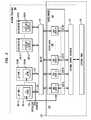
- FIG. 1shows a block diagram of a network processor operating in accordance with exemplary embodiments of the present invention
- FIG. 2shows a block diagram of a system cache of the network processor of FIG. 1 , in accordance with embodiments of the present invention
- FIG. 3shows a block diagram of a memory interface of the system cache of FIG. 2 , in accordance with embodiments of the present invention.
- FIG. 4shows an exemplary flow diagram of a system cache memory access process of the system cache of FIG. 2 .
- Described embodiments of the present inventionprovide for encrypted and non-encrypted operations and debugging operations between an internal memory of a system on chip (SoC) and an external memory of the SoC.
- SoCsystem on chip
- Table 1defines a list of acronyms employed throughout this specification as an aid to understanding the described embodiments of the present invention:
- FIG. 1shows a block diagram of an exemplary network processor system (network processor 100 ) implemented as a system-on-chip (SoC).
- Network processor 100might be used for processing data packets, performing protocol conversion, encrypting and decrypting data packets, or the like.
- network processor 100includes on-chip shared memory 112 , one or more input-output (I/O) interfaces collectively shown as I/O interface 104 , one or more microprocessor ( ⁇ P) cores 106 1 - 106 M , and one or more hardware accelerators 108 1 - 108 N , where M and N are integers greater than or equal to 1.
- Network processor 100also includes external memory interface 114 for communication with external memory 116 .
- External memory 116might typically be implemented as a dynamic random-access memory (DRAM), such as a double-data-rate three (DDR-3) DRAM, for off-chip storage of data.
- DRAMdynamic random-access memory
- DDR-3double-data-rate three
- each of the one or more I/O interfaces, ⁇ P cores and hardware acceleratorsmight be coupled through switch 110 to shared memory 112 .
- Switch 110might be implemented as a non-blocking crossbar switch such as described in related U.S. patent application Ser. Nos. 12/430,438 filed Apr. 27, 2009, 12/729,226 filed Mar. 22, 2010, and 12/729,231 filed Mar. 22, 2010, which are incorporated by reference herein.
- I/O interface 104might typically be implemented as hardware that connects network processor 100 to one or more external devices through I/O communication link 102 .
- I/O communication link 102might generally be employed for communication with one or more external devices, such as a computer system or networking device, which interface with network processor 100 .
- I/O communication link 102might be a custom-designed communication link, or might conform to a standard communication protocol such as, for example, a Small Computer System Interface (“SCSI”) protocol bus, a Serial Attached SCSI (“SAS”) protocol bus, a Serial Advanced Technology Attachment (“SATA”) protocol bus, a Universal Serial Bus (“USB”), an Ethernet link, an IEEE 802.11 link, an IEEE 802.15 link, an IEEE 802.16 link, a Peripheral Component Interconnect Express (“PCI-E”) link, a Serial Rapid I/O (“SRIO”) link, or any other interface link.
- Received packetsare preferably placed in a buffer in shared memory 112 by transfer between I/O interface 104 and shared memory 112 through switch 110 .
- shared memory 112is a conventional memory operating as a cache that might be allocated and/or subdivided.
- shared memory 112might include one or more FIFO queues that might be dynamically allocated to the various ⁇ P cores 106 and hardware accelerators 108 .
- External memory interface 114couples shared memory 112 to one or more external memories, shown as external memory 116 , to provide off-chip storage of data not currently in use by the various ⁇ P cores 106 and hardware accelerators 108 to free space in shared memory 112 .
- Hardware accelerators 108might interact with each other, for example, by one or more communication bus rings 118 that pass “tasks” from a source core to a destination core.
- tasksare instructions to the destination core to perform certain functions, and a task might contain address pointers to data stored in shared memory 112 , as described in related U.S. patent application Ser. Nos. 12/782,379, 12/782,393, and 12/782,411 all filed May 18, 2010, which are incorporated by reference herein.
- Network processor 100might typically receive data packets from one or more source devices, perform processing operations for the received data packets, and transmit data packets out to one or more destination devices. As shown in FIG. 1 , one or more data packets are transmitted from a transmitting device (not shown) to network processor 100 , via I/O communication link 102 . Network processor 100 might receive data packets from one or more active data streams concurrently from I/O communication link 102 . I/O interface 104 might parse the received data packet and provide the received data packet, via switch 110 , to a buffer in shared memory 112 .
- I/O interface 104provides various types of I/O interface functions and, in exemplary embodiments described herein, is a command-driven hardware accelerator that connects network processor 100 to external devices. Received packets are preferably placed in shared memory 112 and then one or more corresponding tasks are generated. Transmitted packets are preferably generated from data in shared memory 112 for one or more corresponding tasks and might be transmitted out of network processor 100 .
- Exemplary I/O interfacesinclude Ethernet I/O adapters providing integrity checks of incoming data. The I/O adapters might also provide timestamp data for received and transmitted packets that might be used to implement features such as timing over packet (e.g., specified in the standard recommendations of IEEE 1588). In alternative embodiments, I/O interface 104 might be implemented as input (receive) only or output (transmit) only interfaces.
- I/O interface 104might also include one or more debug interfaces for interfacing with, for example, development tools of users of network processor 100 , such as a debugger operating in compliance with a Joint Test Action Group (JTAG) interface, a Serial Wire Debug (SWD) interface, or miscellaneous interfaces such as Serial Peripheral Interface (SPI), a Serial Line Internet Protocol (SLIP) interface or a Universal Asynchronous Receiver/Transmitter (UART).
- JTAGJoint Test Action Group
- SWDSerial Wire Debug
- miscellaneous interfacessuch as Serial Peripheral Interface (SPI), a Serial Line Internet Protocol (SLIP) interface or a Universal Asynchronous Receiver/Transmitter (UART).
- JTAGJoint Test Action Group
- SWDSerial Wire Debug
- miscellaneous interfacessuch as Serial Peripheral Interface (SPI), a Serial Line Internet Protocol (SLIP) interface or a Universal Asynchronous Receiver/Transmitter (UART).
- SPISerial Perip
- debugging operationsmight be received via standard communications interfaces, such as a SCSI protocol bus, a SAS protocol bus, a SATA protocol bus, a USB bus, an Ethernet link, an IEEE 802.11 link, an IEEE 802.15 link, an IEEE 802.16 link, a PCI-E link, an SRIO, or other similar interfaces.
- standard communications interfacessuch as a SCSI protocol bus, a SAS protocol bus, a SATA protocol bus, a USB bus, an Ethernet link, an IEEE 802.11 link, an IEEE 802.15 link, an IEEE 802.16 link, a PCI-E link, an SRIO, or other similar interfaces.
- the various ⁇ P cores 106 and hardware accelerators 108 of network processor 100might include several exemplary types of processors or accelerators.
- the various ⁇ P cores 106might be implemented as Pentium® or Power PC® processors, or a combination of different processor types (Pentium® is a registered trademark of Intel Corporation, and Power PC® is a registered trademark of IBM).
- the various hardware accelerators 108might include, for example, one or more function-specific modules, such as a Modular Packet Processor (MPP), a Packet Assembly Block (PAB), a Modular Traffic Manager (MTM), a Memory Management Block (MMB), a Stream Editor (SED), a Security Protocol Processor (SPP), a Regular Expression (RegEx) engine, and other special-purpose modules.
- MPPModular Packet Processor
- PABPacket Assembly Block
- MTMModular Traffic Manager
- MMBMemory Management Block
- SEDSecurity Protocol Processor
- Regular Expression (RegEx) enginea Regular Expression engine
- the MTMis a software-driven accelerator that provides packet scheduling and possibly up to six levels of scheduling hierarchy.
- the MTMmight support millions of queues and schedulers (enabling per flow queuing if desired).
- the MTMmight provide support for shaping and scheduling with smooth deficit weighed round robin (SDWRR) for every queue and scheduler.
- SDWRRsmooth deficit weighed round robin
- the MTMmight also support multicasting. Each copy of a packet is scheduled independently and traverses down one or more virtual pipelines enabling multicast with independent encapsulations or any other processing.
- the MTMmight also contain a special purpose processor that can be used for fine-grained control of scheduling decisions.
- the MTMmight be used to make discard decisions as well as scheduling and shaping decisions.
- the MTMmight operate substantially as described in related U.S.
- the SEDis a software-driven accelerator that allows for editing of packets.
- the SEDperforms packet editing functions that might include adding and modifying packet headers as well as fragmenting or segmenting data (e.g., IP fragmentation).
- the SEDreceives packet data as well as parameters from tasks and a task specified per-flow state.
- the output of the SEDcan become the outgoing packet data and can also update task parameters.
- the RegEx engineis a packet search engine for state-based cross-packet pattern matching.
- the RegEx engineis multi-threaded accelerator.
- An exemplary RegEx enginemight be implemented such as described in U.S. Pat. Nos. 7,439,652 and 7,899,904, the teachings of which are incorporated by reference herein in their entireties.
- the SPPprovides encryption/decryption capabilities and is a command-driven hardware accelerator, preferably having the flexibility to handle protocol variability and changing standards with the ability to add security protocols with firmware upgrades.
- the ciphers and integrity (hash) functionsmight be implemented in hardware.
- the SPPhas a multiple ordered task queue mechanism, discussed in more detail below, that is employed for load balancing across the threads.
- the MMBallocates and frees memory resources in shared memory 112 .
- Memoryis allocated for such applications as task FIFO storage, packet data storage, hash-table collision handling, timer event management, and traffic manager queues.
- the MMBprovides reference counts to each block of memory within shared memory 112 . Multiple reference counts allow for more efficient storage of information, such as multicast traffic (data to be sent to multiple destinations) or for retransmission. Multiple reference counts remove a need for replicating data each time the data is needed.
- the MMBpreferably tracks the memory allocations using a stack-based approach since a memory block recently released is preferably the next block to be allocated for a particular task, reducing cache thrashing and cache tracking overhead.
- Blocks in shared memory 112might be dynamically allocated by the MMB to store data, with the blocks in one of the following sizes: 256, 2048, 16384, and 65536 bytes.
- the MMBmight operate substantially as described in related U.S. patent application Ser. No. 12/963,895 filed Dec. 9, 2010, which is incorporated by reference herein.
- the PABis a command driven hardware accelerator providing a holding buffer with packet assembly, transmit, retransmit, and delete capabilities.
- An incoming task to the PABcan specify to insert/extract data from anywhere in any assembly buffer. Gaps are supported in any buffer. Locations to insert and extract can be specified to the bit level. Exemplary traditional packet reassembly functions might be supported, such as IP defragmentation.
- the PABmight also support generalized holding buffer and sliding window protocol transmit/retransmit buffering, providing an offload for features like TCP origination, termination, and normalization.
- the PABmight operate substantially as described in related U.S. patent application Ser. No. 12/971,742 filed Dec. 17, 2010, which is incorporated by reference herein.
- the MPPis a multi-threaded special purpose processor that provides tree based longest prefix and access control list classification.
- the MPPalso has a hardware hash-based classification capability with full hardware management of hash-table additions, deletions, and collisions.
- Optionally associated with each hash entryis a timer that might be used under software control for tasks such as connection timeout and retransmission timing.
- the MPPcontains a statistics and state management engine, which when combined with the hash table and timer facilities, provides support for state-based protocol processing.
- the MPPmight support millions of flows, limited only by the amount of DRAM capacity assigned to the functions.
- the MPP architecturemight be able to store all per thread states in memory instead of in register files.
- the MPPmight operate substantially as described in related U.S.
- the MPPmight also include hash functionality such as described in related U.S. patent application Ser. Nos. 13/046,717, 13/046,719, and 13/046,726 all filed Mar. 12, 2011, which are incorporated by reference herein.
- FIG. 2shows a block diagram of an exemplary embodiment of system cache 200 of network processor 100 , in accordance with embodiments of the present invention.
- system cache 200might be implemented in shared memory 112 .
- System cache 200might include one or more individual caches, shown as caches 202 ( 1 )- 202 (N).
- Caches 202 ( 1 )- 202 (N)might be employed to cache data from any ⁇ P core or accelerator (e.g., ⁇ P cores 106 or accelerators 108 ) of network processor 100 .
- system cache 200might be employed to store packet data from ⁇ P cores 106 or accelerators 108 .
- ⁇ P core or acceleratore.g., ⁇ P cores 106 or accelerators 108
- caches 202 ( 1 )- 202 (N)might be addressed via switch 110 in such a way as to balance access to the caches, referred to herein as striping, helping to avoid hot spots in shared memory 112 , improve performance of the caching in and out of external memory 116 , and reduce cache access bottlenecks.
- shared memory 112 and external memory 116might generally be referred to as system memory 210 .
- each cache 202 ( 1 )- 202 (N)might form a memory array, and the number of system caches might preferably be implemented as a power of two.
- each cache 202 ( 1 )- 202 (N)might be implemented as an N-way associative cache employing a least recently used (LRU) caching algorithm.
- LRUleast recently used
- each cache 202 ( 1 )- 202 (N)might have a total size of 512 kB and a cache line length of 256B.
- each of ⁇ P cores 106might typically have a corresponding level one (L1) cache, shown as L1 caches 206 ( 1 )- 206 (M). Each of ⁇ P cores 106 might also include a level two (L2) cache (not shown). Such L1 and L2 caches might be implemented in accordance with the processor design of each ⁇ P core 106 , for example a Power PC® processor implementation.
- the various ⁇ P cores 106might be in communication with one another via a communication bus of network processor 100 , for example, a Processor Local Bus (PLB), which is a microprocessor bus architecture introduced by IBM, or an Advanced eXtensible Interface (AXI), which is a higher frequency implementation of the Advanced Microcontroller Bus Architecture (AMBA) introduced by ARM Ltd.
- PLBProcessor Local Bus
- AXIAdvanced eXtensible Interface
- AXIAdvanced Microcontroller Bus Architecture
- one or more of accelerators 108might have one or more corresponding local L1 pipeline caches, shown as L1 pipeline caches 208 ( 1 )- 208 (N).
- L1 pipeline caches 208 ( 1 )- 208 (N)The function of L1 pipeline caches 208 ( 1 )- 208 (N) is to act as an interface to system cache 200 for accelerators 108 of network processor 100 .
- L1 pipeline caches 208 ( 1 )- 208 (N)might typically be employed only for certain ones of accelerators 108 that access system cache 200 as part of an execution pipeline.
- the operation of system cache 200 , shared memory 112 and external memory 116might be substantially as described in related U.S. patent application Ser. Nos. 13/192,104, 13/192,140 and 13/192,187, all filed Jul. 27, 2011, which are incorporated by reference herein.
- FIG. 3shows a block diagram of memory interface 114 of network processor 100 .
- memory interface 114might include non-encrypted data pipeline 302 and encrypted pipeline 304 between system cache 200 and external memory 116 .
- Encrypted data pipeline 304might be optionally employed to encrypt and decrypt data that is transferred between external memory 116 and system cache 200 .
- Some embodiments of encrypted data pipeline 304might selectably employ one or more encryption/decryption methods such as, for example, Specification for the Advanced Encryption Standard ( AES ), Federal Information Processing Standard (FIPS) Publication 197, (2001), published by the National Institute of Standards and Technology (NIST), or other encryption and decryption methods.
- AESAdvanced Encryption Standard
- FIPSFederal Information Processing Standard
- NISTNational Institute of Standards and Technology
- encrypted data pipeline 304might include one or more register stages, shown as register stages 306 ( 1 )- 306 (N), to buffer data as it is encrypted or decrypted by one or more encryption/decryption logic stages, shown as logic stages 308 ( 1 )- 308 (M), where N and M are positive integers.
- Embodiments of the present inventionmight perform encryption for all addresses within external memory 116 , or for one or more programmable regions of the full address space of external memory 116 .
- some data transfer operations between system cache 200 and external memory 116might be encrypted, while others are not encrypted, during standard operation of network processor 100 .
- the data transfer operationis provided to encrypted data pipeline 304 , otherwise, the data transfer operation is provided to non-encrypted data pipeline 302 , which might operation relatively faster than encrypted data pipeline 304 , thus reducing access latency of external memory 116 for non-encrypted data transfers.
- encrypted data pipeline 304is non-empty (e.g., encrypted data pipeline 304 is processing an encrypted data transfer operation)
- non-encrypted operationsmight be stalled until the encrypted data transfer completes, for example by still providing the non-encrypted data transfer operation to encrypted data pipeline 304 .
- Embodiments of the present inventionprovide debugging features for systems that employ data encryption and decryption, such as shown in FIG. 3 .
- encryption and decryption of datatypically involves introduction of additional pipeline and control structures (e.g., encrypted data pipeline 304 ) that might alter the overall flow of data, possibly limiting debugging options for such operations.
- additional pipeline and control structurese.g., encrypted data pipeline 304
- a typical component of encryption and data security implementations in a SoCis to limit external access to on-chip resources, including debug resources, once security is enabled.
- the combination of data encryption and the other security measuresmight make it very difficult to debug a problem in a running system.
- Typical debugging operationsmight simply disable encryption and decryption.
- the SoCmight operate differently. For example, if encryption is disabled for a debugging operation, the SoC might employ non-encrypted data pipeline 302 rather than encrypted data pipeline 304 . Processing modules or state machines of network processor 100 that might perform differently based on whether encryption is enabled or disabled might also function differently during debugging operations. Thus, differences in the observable behavior of the SoC might make diagnosing, identifying and correcting development problems with the SoC difficult when encryption is enabled.
- FIG. 4shows an exemplary flow diagram of the operation of memory interface 114 , for example in processing a data transfer operation between system cache 200 and external memory 116 .
- system cache 200begins operation, for example at power up of network processor 100 .
- system cache 200initiates a data transfer operation with memory interface 114 for external memory 116 , for example to read data from external memory 116 for storage in system cache 200 , or to write data from system cache 200 to external memory 116 .
- memory interface 114determines whether the data transfer operation requires encryption (e.g., to write to external memory 116 ) or decryption (e.g., to read from external memory 116 ).
- the data transfer operationis provided to encrypted data pipeline 304 at step 412 .
- encrypted data pipeline 304determines whether the data transfer operation corresponds to a debugging operation, or if the data transfer operation corresponds to a normal data transfer operation of network processor 100 .
- the data transfer operationis provided to external memory 116 , and data encryption (e.g., for write operations to external memory 116 ) or decryption (e.g., for read operations from external memory 116 ) is performed for the data transfer at step 420 .
- system cache operation 400completes at step 422 .
- the debugging operationis provided to encrypted data pipeline 304 .
- Encrypted data pipeline 304at each of logic stages 308 , determines that the operation is a debugging operation and bypasses actually performing encryption or decryption of the data transfer operation, but still passing the data transfer operation through each of register stages 306 and logic stages 308 .
- Various stage machines of encrypted data pipeline 304operate substantially similarly regardless of whether encryption is enabled.
- the data transfer operationis provided to non-encrypted data pipeline 302 at step 408 .
- encrypted data pipeline 304is non-empty (e.g., encrypted data pipeline 304 is processing an encrypted data transfer operation)
- non-encrypted operationsmight be stalled until the encrypted data transfer completes, for example by still providing the non-encrypted data transfer operation to encrypted data pipeline 304 .
- the data transfer operationis provided to external memory 116 via non-encrypted data pipeline 302 .
- the data transfer operationis processed by external memory 116 , for example, by writing non-encrypted data to external memory 116 , or by providing non-encrypted data from external memory 116 to non-encrypted data pipeline 302 .
- system cache operation 400completes at step 422 .
- the one or more indicators employed at steps 406 and 414might be implemented as one or more indicator bit flags of control data for each corresponding data transfer operation.
- some embodimentsmight employ a debug indicator bit flag that, when set, indicates that the corresponding data transfer operation is a debugging operation, and an encryption or security bit flag that, when set, indicate that encryption or other security measures are to be employed for the data transfer operation.
- described embodimentsprovide substantially the same data flow for data transfer operations between system cache 200 and external memory 116 regardless of whether the operation is a debugging operation or a standard operation of network processor 100 .
- the data flowcan be substantially duplicated whether encryption is enabled or disabled as part of an overall security plan of network processor 100 since the pipeline data flows are substantially similar (e.g., through the corresponding one of pipelines 302 and 304 ), and the one or more corresponding state machines operate substantially similarly regardless of the operation being a debugging operation or not.
- debugging operationsmight not perform actual data encryption and decryption, the various register stages 306 and logic stages 308 process a debugging operation substantially similarly as a non-debugging operation.
- references herein to “one embodiment” or “an embodiment”means that a particular feature, structure, or characteristic described in connection with the embodiment can be included in at least one embodiment of the invention.
- the appearances of the phrase “in one embodiment” in various places in the specificationare not necessarily all referring to the same embodiment, nor are separate or alternative embodiments necessarily mutually exclusive of other embodiments.
- the word “exemplary”is used herein to mean serving as an example, instance, or illustration. Any aspect or design described herein as “exemplary” is not necessarily to be construed as preferred or advantageous over other aspects or designs. Rather, use of the word exemplary is intended to present concepts in a concrete fashion.
- the term “or”is intended to mean an inclusive “or” rather than an exclusive “or”. That is, unless specified otherwise, or clear from context, “X employs A or B” is intended to mean any of the natural inclusive permutations. That is, if X employs A; X employs B; or X employs both A and B, then “X employs A or B” is satisfied under any of the foregoing instances.
- the articles “a” and “an” as used in this application and the appended claimsshould generally be construed to mean “one or more” unless specified otherwise or clear from context to be directed to a singular form.
- a componentmay be, but is not limited to being, a process running on a processor, a processor, an object, an executable, a thread of execution, a program, and/or a computer.
- an application running on a controller and the controllercan be a component.
- One or more componentsmay reside within a process and/or thread of execution and a component may be localized on one computer and/or distributed between two or more computers.
- the term “compatible”means that the element communicates with other elements in a manner wholly or partially specified by the standard, and would be recognized by other elements as sufficiently capable of communicating with the other elements in the manner specified by the standard.
- the compatible elementdoes not need to operate internally in a manner specified by the standard.
- Couplerefers to any manner known in the art or later developed in which energy is allowed to be transferred between two or more elements, and the interposition of one or more additional elements is contemplated, although not required.
- the terms “directly coupled,” “directly connected,” etc.imply the absence of such additional elements. Signals and corresponding nodes or ports might be referred to by the same name and are interchangeable for purposes here.
- the present inventioncan be embodied in the form of methods and apparatuses for practicing those methods.
- the present inventioncan also be embodied in the form of program code embodied in tangible media, such as magnetic recording media, optical recording media, solid state memory, floppy diskettes, CD-ROMs, hard drives, or any other non-transitory machine-readable storage medium, wherein, when the program code is loaded into and executed by a machine, such as a computer, the machine becomes an apparatus for practicing the invention.
- the present inventioncan also be embodied in the form of program code, for example, whether stored in a non-transitory machine-readable storage medium, loaded into and/or executed by a machine, or transmitted over some transmission medium or carrier, such as over electrical wiring or cabling, through fiber optics, or via electromagnetic radiation, wherein, when the program code is loaded into and executed by a machine, such as a computer, the machine becomes an apparatus for practicing the invention.
- program codeWhen implemented on a general-purpose processor, the program code segments combine with the processor to provide a unique device that operates analogously to specific logic circuits.
- the present inventioncan also be embodied in the form of a bitstream or other sequence of signal values electrically or optically transmitted through a medium, stored magnetic-field variations in a magnetic recording medium, etc., generated using a method and/or an apparatus of the present invention.
Landscapes
- Engineering & Computer Science (AREA)
- Computer Networks & Wireless Communication (AREA)
- Signal Processing (AREA)
- Physics & Mathematics (AREA)
- Computer Hardware Design (AREA)
- Theoretical Computer Science (AREA)
- Mathematical Physics (AREA)
- Software Systems (AREA)
- General Engineering & Computer Science (AREA)
- General Physics & Mathematics (AREA)
- Memory System Of A Hierarchy Structure (AREA)
Abstract
Description
| TABLE 1 | |||
| USB | Universal Serial Bus | FIFO | First-In, First-Out |
| SATA | Serial Advanced Technology | I/O | Input/Output |
| Attachment | |||
| SCSI | Small Computer System Interface | DDR | Double Data Rate |
| SAS | Serial Attached SCSI | DRAM | Dynamic Random Access Memory |
| PCI-E | Peripheral Component | MMB | Memory Manager Block |
| Interconnect Express | |||
| SRIO | Serial RapidIO | CPU | Central Processing Unit |
| SoC | System-on-Chip | μP | Microprocessor |
| AXI | Advanced eXtensible Interface | PLB | Processor Local Bus |
| AMBA | Advanced Microcontroller Bus | MPP | Modular Packet Processor |
| Architecture | |||
| PAB | Packet Assembly Block | SED | Stream Editor |
| MTM | Modular Traffic Manager | ||
| TCP | Transmission Control Protocol | CRC | Cyclic Redundancy Check |
| API | Application Programming | UART | Universal Asynchronous |
| Interfaces | Receiver/Transmitter | ||
| SWD | Serial Wire Debug | JTAG | Joint Test Action Group |
| IP | Internet Protocol | SLIP | Serial Line Internet Protocol |
Claims (18)
Priority Applications (6)
| Application Number | Priority Date | Filing Date | Title |
|---|---|---|---|
| US13/274,726US8683221B2 (en) | 2010-05-18 | 2011-10-17 | Configurable memory encryption with constant pipeline delay in a multi-core processor |
| US13/310,961US9300597B2 (en) | 2009-04-27 | 2011-12-05 | Statistics module for network processors in virtual local area networks |
| US13/316,145US9195464B2 (en) | 2009-04-27 | 2011-12-09 | Tracking written addresses of a shared memory of a multi-core processor |
| US13/687,958US9461930B2 (en) | 2009-04-27 | 2012-11-28 | Modifying data streams without reordering in a multi-thread, multi-flow network processor |
| US13/705,822US9727508B2 (en) | 2009-04-27 | 2012-12-05 | Address learning and aging for network bridging in a network processor |
| US13/756,849US9444737B2 (en) | 2009-04-27 | 2013-02-01 | Packet data processor in a communications processor architecture |
Applications Claiming Priority (4)
| Application Number | Priority Date | Filing Date | Title |
|---|---|---|---|
| US12/782,411US8407707B2 (en) | 2009-05-18 | 2010-05-18 | Task queuing in a network communications processor architecture |
| US12/782,379US9081742B2 (en) | 2009-04-27 | 2010-05-18 | Network communications processor architecture |
| US12/782,393US8255644B2 (en) | 2009-05-18 | 2010-05-18 | Network communications processor architecture with memory load balancing |
| US13/274,726US8683221B2 (en) | 2010-05-18 | 2011-10-17 | Configurable memory encryption with constant pipeline delay in a multi-core processor |
Related Parent Applications (1)
| Application Number | Title | Priority Date | Filing Date |
|---|---|---|---|
| US12/782,379Continuation-In-PartUS9081742B2 (en) | 2009-04-27 | 2010-05-18 | Network communications processor architecture |
Publications (2)
| Publication Number | Publication Date |
|---|---|
| US20120036351A1 US20120036351A1 (en) | 2012-02-09 |
| US8683221B2true US8683221B2 (en) | 2014-03-25 |
Family
ID=45556972
Family Applications (1)
| Application Number | Title | Priority Date | Filing Date |
|---|---|---|---|
| US13/274,726Expired - Fee RelatedUS8683221B2 (en) | 2009-04-27 | 2011-10-17 | Configurable memory encryption with constant pipeline delay in a multi-core processor |
Country Status (1)
| Country | Link |
|---|---|
| US (1) | US8683221B2 (en) |
Cited By (5)
| Publication number | Priority date | Publication date | Assignee | Title |
|---|---|---|---|---|
| US20130018978A1 (en)* | 2011-01-28 | 2013-01-17 | Level 3 Communications, Llc | Content delivery network with deep caching infrastructure |
| US20130198293A1 (en)* | 2012-01-27 | 2013-08-01 | Microsoft Corporation | Techniques to distribute messages using communication pipelines |
| CN104991845A (en)* | 2015-06-24 | 2015-10-21 | 福州瑞芯微电子有限公司 | High-speed debug method and apparatus for multi-core chip |
| US9621669B2 (en) | 2011-01-28 | 2017-04-11 | Level 3 Communications, Llc | Content delivery network with deep caching infrastructure |
| US20230067432A1 (en)* | 2020-04-29 | 2023-03-02 | Stream Computing Inc. | Task allocation method, apparatus, electronic device, and computer-readable storage medium |
Families Citing this family (8)
| Publication number | Priority date | Publication date | Assignee | Title |
|---|---|---|---|---|
| CN102752166B (en)* | 2012-05-31 | 2015-03-18 | 华为技术有限公司 | Debugging method, chip, single board and system |
| EP2672673B1 (en)* | 2012-06-07 | 2016-05-25 | Alcatel Lucent | Apparatus and method for secure data processing |
| WO2014210277A1 (en) | 2013-06-28 | 2014-12-31 | The Trustees Of Columbia University In The City Of New York | Diversified instruction set processing to enhance security |
| US9684578B2 (en)* | 2014-10-30 | 2017-06-20 | Qualcomm Incorporated | Embedded universal serial bus (USB) debug (EUD) for multi-interfaced debugging in electronic systems |
| US10969991B2 (en)* | 2018-08-15 | 2021-04-06 | Macronix International Co., Ltd. | Multi-chip package, controlling method of multi-chip package and security chip |
| TWI733375B (en)* | 2020-03-17 | 2021-07-11 | 群聯電子股份有限公司 | Data transfer method and memory storage device |
| CN112019457B (en)* | 2020-08-31 | 2022-09-06 | 北京计算机技术及应用研究所 | High-speed switching device based on localization SRIO |
| US20230015697A1 (en)* | 2021-07-13 | 2023-01-19 | Citrix Systems, Inc. | Application programming interface (api) authorization |
Citations (38)
| Publication number | Priority date | Publication date | Assignee | Title |
|---|---|---|---|---|
| US4622631A (en) | 1983-12-30 | 1986-11-11 | Plexus Computers, Inc. | Data processing system having a data coherence solution |
| JPH02271444A (en) | 1989-04-13 | 1990-11-06 | Koufu Nippon Denki Kk | Address converting circuit |
| US5623698A (en) | 1993-04-30 | 1997-04-22 | Cray Research, Inc. | Memory interconnect network having separate routing networks for inputs and outputs using switches with FIFO queues and message steering bits |
| US5825878A (en)* | 1996-09-20 | 1998-10-20 | Vlsi Technology, Inc. | Secure memory management unit for microprocessor |
| US5892766A (en) | 1996-02-22 | 1999-04-06 | Fujitsu, Ltd. | Method and apparatus for coordinating access to an output of a routing device in a packet switching network |
| US5943283A (en) | 1997-12-05 | 1999-08-24 | Invox Technology | Address scrambling in a semiconductor memory |
| US6038630A (en) | 1998-03-24 | 2000-03-14 | International Business Machines Corporation | Shared access control device for integrated system with multiple functional units accessing external structures over multiple data buses |
| US6195335B1 (en) | 1997-06-27 | 2001-02-27 | International Business Machines Corporation | Data switch |
| US20020029214A1 (en) | 2000-08-10 | 2002-03-07 | Nec Corporation | Synchronizable transactional database method and system |
| US20020122671A1 (en)* | 2001-02-19 | 2002-09-05 | Canon Kabushiki Kaisha | Unit and image processing apparatus |
| US20020165985A1 (en) | 2001-05-03 | 2002-11-07 | Jen-Kai Chen | Method for accessing a non-symmetric dual-slot address table and switching apparatus using same |
| US20030033276A1 (en) | 2001-08-09 | 2003-02-13 | Integrated Silicon Solution, Inc. | Search engine for large database search using CAM and hash |
| US6567564B1 (en) | 1996-04-17 | 2003-05-20 | Sarnoff Corporation | Pipelined pyramid processor for image processing systems |
| US20030115417A1 (en) | 2001-12-17 | 2003-06-19 | Corrigan Brian E. | Methods and apparatus for loading CRC values into a CRC cache in a storage controller |
| US20030123468A1 (en) | 2001-12-31 | 2003-07-03 | Stmicroelectronics, Inc. | Apparatus for switching data in high-speed networks and method of operation |
| US6636932B1 (en) | 1998-05-27 | 2003-10-21 | Micron Technology, Inc. | Crossbar switch and control for data networks switching |
| US20040255209A1 (en) | 2003-06-10 | 2004-12-16 | Fred Gross | Apparatus and method for compressing redundancy information for embedded memories, including cache memories, of integrated circuits |
| US20050027920A1 (en) | 2003-07-31 | 2005-02-03 | Fitzsimmons Michael D. | Crossbar switch that supports a multi-port slave device and method of operation |
| US20050152352A1 (en) | 2003-12-27 | 2005-07-14 | Jong-Arm Jun | Scalable crossbar matrix switching apparatus and distributed scheduling method thereof |
| US7089346B2 (en) | 2002-06-03 | 2006-08-08 | International Business Machines Corporation | Method of operating a crossbar switch |
| US7096370B1 (en)* | 1999-03-26 | 2006-08-22 | Micron Technology, Inc. | Data security for digital data storage |
| US20060256783A1 (en) | 2005-04-06 | 2006-11-16 | Robert Ayrapetian | Buffered crossbar switch with a linear buffer to port relationship that supports cells and packets of variable size |
| US20070016756A1 (en) | 2005-07-15 | 2007-01-18 | Jen-Wei Hsieh | Device for identifying data characteristics for flash memory |
| US20070016835A1 (en)* | 2005-07-12 | 2007-01-18 | Integrated Device Technology, Inc. | Method and apparatus for parameter adjustment, testing, and configuration |
| US7234018B1 (en) | 2001-07-11 | 2007-06-19 | Pasternak Solutions Llc | Layered crossbar for interconnection of multiple processors and shared memories |
| US20070226798A1 (en) | 1999-07-29 | 2007-09-27 | Intertrust Technologies Corporation | Systems and methods for using cryptography to protect secure and insecure computing environments |
| US7334178B1 (en)* | 2005-09-09 | 2008-02-19 | Xsigo Systems | Randomized self-checking test system |
| US20080162793A1 (en) | 2006-12-28 | 2008-07-03 | Genesys Logic, Inc. | Management method for reducing utilization rate of random access memory (ram) used in flash memory |
| US7461407B2 (en) | 2004-02-05 | 2008-12-02 | Research In Motion Limited | Debugging port security interface |
| US7461208B1 (en) | 2005-06-16 | 2008-12-02 | Sun Microsystems, Inc. | Circuitry and method for accessing an associative cache with parallel determination of data and data availability |
| US20090019270A1 (en) | 2007-07-13 | 2009-01-15 | Digi International Inc. | Embedded device program debug control |
| US7596142B1 (en) | 2006-05-12 | 2009-09-29 | Integrated Device Technology, Inc | Packet processing in a packet switch with improved output data distribution |
| US7694152B2 (en)* | 2005-02-03 | 2010-04-06 | International Business Machines Corporation | Memory controller with performance-modulated security |
| US7779273B2 (en)* | 2006-06-09 | 2010-08-17 | International Business Machines Corporation | Booting a multiprocessor device based on selection of encryption keys to be provided to processors |
| US20100260198A1 (en) | 2009-04-08 | 2010-10-14 | Roberto Rojas-Cessa | Space-Space-Memory (SSM) Clos-Network Packet Switch |
| US7849315B2 (en) | 2006-05-22 | 2010-12-07 | General Dynamics C4 Systems, Inc. | Method for managing operability of on-chip debug capability |
| US7886150B2 (en) | 2007-05-11 | 2011-02-08 | Mips Technologies, Inc. | System debug and trace system and method, and applications thereof |
| US8271805B2 (en)* | 2005-02-04 | 2012-09-18 | Sony Computer Entertainment Inc. | Methods and apparatus for providing a secure buffer |
- 2011
- 2011-10-17USUS13/274,726patent/US8683221B2/ennot_activeExpired - Fee Related
Patent Citations (40)
| Publication number | Priority date | Publication date | Assignee | Title |
|---|---|---|---|---|
| US4622631B1 (en) | 1983-12-30 | 1996-04-09 | Recognition Int Inc | Data processing system having a data coherence solution |
| US4622631A (en) | 1983-12-30 | 1986-11-11 | Plexus Computers, Inc. | Data processing system having a data coherence solution |
| JPH02271444A (en) | 1989-04-13 | 1990-11-06 | Koufu Nippon Denki Kk | Address converting circuit |
| US5623698A (en) | 1993-04-30 | 1997-04-22 | Cray Research, Inc. | Memory interconnect network having separate routing networks for inputs and outputs using switches with FIFO queues and message steering bits |
| US5892766A (en) | 1996-02-22 | 1999-04-06 | Fujitsu, Ltd. | Method and apparatus for coordinating access to an output of a routing device in a packet switching network |
| US6567564B1 (en) | 1996-04-17 | 2003-05-20 | Sarnoff Corporation | Pipelined pyramid processor for image processing systems |
| US5825878A (en)* | 1996-09-20 | 1998-10-20 | Vlsi Technology, Inc. | Secure memory management unit for microprocessor |
| US6195335B1 (en) | 1997-06-27 | 2001-02-27 | International Business Machines Corporation | Data switch |
| US5943283A (en) | 1997-12-05 | 1999-08-24 | Invox Technology | Address scrambling in a semiconductor memory |
| US6038630A (en) | 1998-03-24 | 2000-03-14 | International Business Machines Corporation | Shared access control device for integrated system with multiple functional units accessing external structures over multiple data buses |
| US6636932B1 (en) | 1998-05-27 | 2003-10-21 | Micron Technology, Inc. | Crossbar switch and control for data networks switching |
| US7096370B1 (en)* | 1999-03-26 | 2006-08-22 | Micron Technology, Inc. | Data security for digital data storage |
| US20070226798A1 (en) | 1999-07-29 | 2007-09-27 | Intertrust Technologies Corporation | Systems and methods for using cryptography to protect secure and insecure computing environments |
| US20020029214A1 (en) | 2000-08-10 | 2002-03-07 | Nec Corporation | Synchronizable transactional database method and system |
| US20020122671A1 (en)* | 2001-02-19 | 2002-09-05 | Canon Kabushiki Kaisha | Unit and image processing apparatus |
| US20020165985A1 (en) | 2001-05-03 | 2002-11-07 | Jen-Kai Chen | Method for accessing a non-symmetric dual-slot address table and switching apparatus using same |
| US7234018B1 (en) | 2001-07-11 | 2007-06-19 | Pasternak Solutions Llc | Layered crossbar for interconnection of multiple processors and shared memories |
| US20030033276A1 (en) | 2001-08-09 | 2003-02-13 | Integrated Silicon Solution, Inc. | Search engine for large database search using CAM and hash |
| US20030115417A1 (en) | 2001-12-17 | 2003-06-19 | Corrigan Brian E. | Methods and apparatus for loading CRC values into a CRC cache in a storage controller |
| US20030123468A1 (en) | 2001-12-31 | 2003-07-03 | Stmicroelectronics, Inc. | Apparatus for switching data in high-speed networks and method of operation |
| US7089346B2 (en) | 2002-06-03 | 2006-08-08 | International Business Machines Corporation | Method of operating a crossbar switch |
| US20040255209A1 (en) | 2003-06-10 | 2004-12-16 | Fred Gross | Apparatus and method for compressing redundancy information for embedded memories, including cache memories, of integrated circuits |
| US20050027920A1 (en) | 2003-07-31 | 2005-02-03 | Fitzsimmons Michael D. | Crossbar switch that supports a multi-port slave device and method of operation |
| US20050152352A1 (en) | 2003-12-27 | 2005-07-14 | Jong-Arm Jun | Scalable crossbar matrix switching apparatus and distributed scheduling method thereof |
| US7461407B2 (en) | 2004-02-05 | 2008-12-02 | Research In Motion Limited | Debugging port security interface |
| US20090132827A1 (en)* | 2004-02-05 | 2009-05-21 | Research In Motion Limited | Debugging port security interface |
| US7694152B2 (en)* | 2005-02-03 | 2010-04-06 | International Business Machines Corporation | Memory controller with performance-modulated security |
| US8271805B2 (en)* | 2005-02-04 | 2012-09-18 | Sony Computer Entertainment Inc. | Methods and apparatus for providing a secure buffer |
| US20060256783A1 (en) | 2005-04-06 | 2006-11-16 | Robert Ayrapetian | Buffered crossbar switch with a linear buffer to port relationship that supports cells and packets of variable size |
| US7461208B1 (en) | 2005-06-16 | 2008-12-02 | Sun Microsystems, Inc. | Circuitry and method for accessing an associative cache with parallel determination of data and data availability |
| US20070016835A1 (en)* | 2005-07-12 | 2007-01-18 | Integrated Device Technology, Inc. | Method and apparatus for parameter adjustment, testing, and configuration |
| US20070016756A1 (en) | 2005-07-15 | 2007-01-18 | Jen-Wei Hsieh | Device for identifying data characteristics for flash memory |
| US7334178B1 (en)* | 2005-09-09 | 2008-02-19 | Xsigo Systems | Randomized self-checking test system |
| US7596142B1 (en) | 2006-05-12 | 2009-09-29 | Integrated Device Technology, Inc | Packet processing in a packet switch with improved output data distribution |
| US7849315B2 (en) | 2006-05-22 | 2010-12-07 | General Dynamics C4 Systems, Inc. | Method for managing operability of on-chip debug capability |
| US7779273B2 (en)* | 2006-06-09 | 2010-08-17 | International Business Machines Corporation | Booting a multiprocessor device based on selection of encryption keys to be provided to processors |
| US20080162793A1 (en) | 2006-12-28 | 2008-07-03 | Genesys Logic, Inc. | Management method for reducing utilization rate of random access memory (ram) used in flash memory |
| US7886150B2 (en) | 2007-05-11 | 2011-02-08 | Mips Technologies, Inc. | System debug and trace system and method, and applications thereof |
| US20090019270A1 (en) | 2007-07-13 | 2009-01-15 | Digi International Inc. | Embedded device program debug control |
| US20100260198A1 (en) | 2009-04-08 | 2010-10-14 | Roberto Rojas-Cessa | Space-Space-Memory (SSM) Clos-Network Packet Switch |
Cited By (11)
| Publication number | Priority date | Publication date | Assignee | Title |
|---|---|---|---|---|
| US20130018978A1 (en)* | 2011-01-28 | 2013-01-17 | Level 3 Communications, Llc | Content delivery network with deep caching infrastructure |
| US9161080B2 (en)* | 2011-01-28 | 2015-10-13 | Level 3 Communications, Llc | Content delivery network with deep caching infrastructure |
| US9621669B2 (en) | 2011-01-28 | 2017-04-11 | Level 3 Communications, Llc | Content delivery network with deep caching infrastructure |
| US9871881B2 (en) | 2011-01-28 | 2018-01-16 | Level 3 Communications, Llc | Content delivery network with deep caching infrastructure |
| US10356201B2 (en) | 2011-01-28 | 2019-07-16 | Level 3 Communications, Llc | Content delivery network with deep caching infrastructure |
| US10893118B2 (en) | 2011-01-28 | 2021-01-12 | Level 3 Communications, Llc | Content delivery network with deep caching infrastructure |
| US20130198293A1 (en)* | 2012-01-27 | 2013-08-01 | Microsoft Corporation | Techniques to distribute messages using communication pipelines |
| US9203780B2 (en)* | 2012-01-27 | 2015-12-01 | Microsoft Technology Licensing, Llc | Techniques to distribute messages using communication pipelines |
| CN104991845A (en)* | 2015-06-24 | 2015-10-21 | 福州瑞芯微电子有限公司 | High-speed debug method and apparatus for multi-core chip |
| CN104991845B (en)* | 2015-06-24 | 2018-10-23 | 福州瑞芯微电子股份有限公司 | Soc multi core chip high speed debug method and devices |
| US20230067432A1 (en)* | 2020-04-29 | 2023-03-02 | Stream Computing Inc. | Task allocation method, apparatus, electronic device, and computer-readable storage medium |
Also Published As
| Publication number | Publication date |
|---|---|
| US20120036351A1 (en) | 2012-02-09 |
Similar Documents
| Publication | Publication Date | Title |
|---|---|---|
| US8683221B2 (en) | Configurable memory encryption with constant pipeline delay in a multi-core processor | |
| US9444757B2 (en) | Dynamic configuration of processing modules in a network communications processor architecture | |
| US8910168B2 (en) | Task backpressure and deletion in a multi-flow network processor architecture | |
| US8917738B2 (en) | Multicasting traffic manager in a network communications processor architecture | |
| US9444737B2 (en) | Packet data processor in a communications processor architecture | |
| US9081742B2 (en) | Network communications processor architecture | |
| US9183145B2 (en) | Data caching in a network communications processor architecture | |
| US9218290B2 (en) | Data caching in a network communications processor architecture | |
| US8761204B2 (en) | Packet assembly module for multi-core, multi-thread network processors | |
| US8949838B2 (en) | Multi-threaded processing with hardware accelerators | |
| US9461930B2 (en) | Modifying data streams without reordering in a multi-thread, multi-flow network processor | |
| US8499137B2 (en) | Memory manager for a network communications processor architecture | |
| US8539199B2 (en) | Hash processing in a network communications processor architecture | |
| US9154442B2 (en) | Concurrent linked-list traversal for real-time hash processing in multi-core, multi-thread network processors | |
| US8949582B2 (en) | Changing a flow identifier of a packet in a multi-thread, multi-flow network processor | |
| US8321385B2 (en) | Hash processing in a network communications processor architecture | |
| US8873550B2 (en) | Task queuing in a multi-flow network processor architecture | |
| US9300597B2 (en) | Statistics module for network processors in virtual local area networks | |
| JP6676027B2 (en) | Multi-core interconnection in network processors | |
| US9152564B2 (en) | Early cache eviction in a multi-flow network processor architecture | |
| US8943507B2 (en) | Packet assembly module for multi-core, multi-thread network processors | |
| US8677075B2 (en) | Memory manager for a network communications processor architecture | |
| US8874878B2 (en) | Thread synchronization in a multi-thread, multi-flow network communications processor architecture | |
| US9195464B2 (en) | Tracking written addresses of a shared memory of a multi-core processor |
Legal Events
| Date | Code | Title | Description |
|---|---|---|---|
| AS | Assignment | Owner name:LSI CORPORATION, CALIFORNIA Free format text:ASSIGNMENT OF ASSIGNORS INTEREST;ASSIGNORS:PEET, JR., CHARLES EDWARD;BETKER, MICHAEL;SIGNING DATES FROM 20111014 TO 20111017;REEL/FRAME:027071/0530 | |
| STCF | Information on status: patent grant | Free format text:PATENTED CASE | |
| AS | Assignment | Owner name:DEUTSCHE BANK AG NEW YORK BRANCH, AS COLLATERAL AG Free format text:PATENT SECURITY AGREEMENT;ASSIGNORS:LSI CORPORATION;AGERE SYSTEMS LLC;REEL/FRAME:032856/0031 Effective date:20140506 | |
| AS | Assignment | Owner name:LSI CORPORATION, CALIFORNIA Free format text:TERMINATION AND RELEASE OF SECURITY INTEREST IN PATENTS AT REEL/FRAME NO. 32856/0031;ASSIGNOR:DEUTSCHE BANK AG NEW YORK BRANCH;REEL/FRAME:034286/0872 Effective date:20141118 Owner name:AGERE SYSTEMS LLC, PENNSYLVANIA Free format text:TERMINATION AND RELEASE OF SECURITY INTEREST IN PATENTS AT REEL/FRAME NO. 32856/0031;ASSIGNOR:DEUTSCHE BANK AG NEW YORK BRANCH;REEL/FRAME:034286/0872 Effective date:20141118 | |
| FEPP | Fee payment procedure | Free format text:PAYOR NUMBER ASSIGNED (ORIGINAL EVENT CODE: ASPN); ENTITY STATUS OF PATENT OWNER: LARGE ENTITY Free format text:PAYER NUMBER DE-ASSIGNED (ORIGINAL EVENT CODE: RMPN); ENTITY STATUS OF PATENT OWNER: LARGE ENTITY | |
| AS | Assignment | Owner name:INTEL CORPORATION, CALIFORNIA Free format text:ASSIGNMENT OF ASSIGNORS INTEREST;ASSIGNOR:LSI CORPORATION;REEL/FRAME:035090/0477 Effective date:20141114 | |
| AS | Assignment | Owner name:LSI CORPORATION, CALIFORNIA Free format text:TERMINATION AND RELEASE OF SECURITY INTEREST IN PATENT RIGHTS (RELEASES RF 032856-0031);ASSIGNOR:DEUTSCHE BANK AG NEW YORK BRANCH, AS COLLATERAL AGENT;REEL/FRAME:037684/0039 Effective date:20160201 Owner name:AGERE SYSTEMS LLC, PENNSYLVANIA Free format text:TERMINATION AND RELEASE OF SECURITY INTEREST IN PATENT RIGHTS (RELEASES RF 032856-0031);ASSIGNOR:DEUTSCHE BANK AG NEW YORK BRANCH, AS COLLATERAL AGENT;REEL/FRAME:037684/0039 Effective date:20160201 | |
| MAFP | Maintenance fee payment | Free format text:PAYMENT OF MAINTENANCE FEE, 4TH YEAR, LARGE ENTITY (ORIGINAL EVENT CODE: M1551) Year of fee payment:4 | |
| FEPP | Fee payment procedure | Free format text:MAINTENANCE FEE REMINDER MAILED (ORIGINAL EVENT CODE: REM.); ENTITY STATUS OF PATENT OWNER: LARGE ENTITY | |
| LAPS | Lapse for failure to pay maintenance fees | Free format text:PATENT EXPIRED FOR FAILURE TO PAY MAINTENANCE FEES (ORIGINAL EVENT CODE: EXP.); ENTITY STATUS OF PATENT OWNER: LARGE ENTITY | |
| STCH | Information on status: patent discontinuation | Free format text:PATENT EXPIRED DUE TO NONPAYMENT OF MAINTENANCE FEES UNDER 37 CFR 1.362 | |
| FP | Lapsed due to failure to pay maintenance fee | Effective date:20220325 |