US8681422B2 - Optical processing device employing a digital micromirror device (DMD) and having reduced wavelength dependent loss - Google Patents
Optical processing device employing a digital micromirror device (DMD) and having reduced wavelength dependent lossDownload PDFInfo
- Publication number
- US8681422B2 US8681422B2US13/325,555US201113325555AUS8681422B2US 8681422 B2US8681422 B2US 8681422B2US 201113325555 AUS201113325555 AUS 201113325555AUS 8681422 B2US8681422 B2US 8681422B2
- Authority
- US
- United States
- Prior art keywords
- optical
- optical element
- wavelength
- actuatable
- wavelength components
- Prior art date
- Legal status (The legal status is an assumption and is not a legal conclusion. Google has not performed a legal analysis and makes no representation as to the accuracy of the status listed.)
- Active, expires
Links
Images


Classifications
- G—PHYSICS
- G02—OPTICS
- G02B—OPTICAL ELEMENTS, SYSTEMS OR APPARATUS
- G02B5/00—Optical elements other than lenses
- G02B5/18—Diffraction gratings
- G—PHYSICS
- G02—OPTICS
- G02B—OPTICAL ELEMENTS, SYSTEMS OR APPARATUS
- G02B6/00—Light guides; Structural details of arrangements comprising light guides and other optical elements, e.g. couplings
- G02B6/24—Coupling light guides
- G02B6/26—Optical coupling means
- G02B6/28—Optical coupling means having data bus means, i.e. plural waveguides interconnected and providing an inherently bidirectional system by mixing and splitting signals
- G02B6/293—Optical coupling means having data bus means, i.e. plural waveguides interconnected and providing an inherently bidirectional system by mixing and splitting signals with wavelength selective means
- G02B6/29304—Optical coupling means having data bus means, i.e. plural waveguides interconnected and providing an inherently bidirectional system by mixing and splitting signals with wavelength selective means operating by diffraction, e.g. grating
- G02B6/29305—Optical coupling means having data bus means, i.e. plural waveguides interconnected and providing an inherently bidirectional system by mixing and splitting signals with wavelength selective means operating by diffraction, e.g. grating as bulk element, i.e. free space arrangement external to a light guide
- G02B6/29313—Optical coupling means having data bus means, i.e. plural waveguides interconnected and providing an inherently bidirectional system by mixing and splitting signals with wavelength selective means operating by diffraction, e.g. grating as bulk element, i.e. free space arrangement external to a light guide characterised by means for controlling the position or direction of light incident to or leaving the diffractive element, e.g. for varying the wavelength response
- G02B6/29314—Optical coupling means having data bus means, i.e. plural waveguides interconnected and providing an inherently bidirectional system by mixing and splitting signals with wavelength selective means operating by diffraction, e.g. grating as bulk element, i.e. free space arrangement external to a light guide characterised by means for controlling the position or direction of light incident to or leaving the diffractive element, e.g. for varying the wavelength response by moving or modifying the diffractive element, e.g. deforming
- G—PHYSICS
- G02—OPTICS
- G02B—OPTICAL ELEMENTS, SYSTEMS OR APPARATUS
- G02B5/00—Optical elements other than lenses
- G02B5/08—Mirrors
- G—PHYSICS
- G02—OPTICS
- G02B—OPTICAL ELEMENTS, SYSTEMS OR APPARATUS
- G02B6/00—Light guides; Structural details of arrangements comprising light guides and other optical elements, e.g. couplings
- G02B6/24—Coupling light guides
- G02B6/26—Optical coupling means
- G02B6/35—Optical coupling means having switching means
- G02B6/351—Optical coupling means having switching means involving stationary waveguides with moving interposed optical elements
- G02B6/3512—Optical coupling means having switching means involving stationary waveguides with moving interposed optical elements the optical element being reflective, e.g. mirror
- G02B6/3518—Optical coupling means having switching means involving stationary waveguides with moving interposed optical elements the optical element being reflective, e.g. mirror the reflective optical element being an intrinsic part of a MEMS device, i.e. fabricated together with the MEMS device
- G—PHYSICS
- G02—OPTICS
- G02B—OPTICAL ELEMENTS, SYSTEMS OR APPARATUS
- G02B6/00—Light guides; Structural details of arrangements comprising light guides and other optical elements, e.g. couplings
- G02B6/24—Coupling light guides
- G02B6/26—Optical coupling means
- G02B6/35—Optical coupling means having switching means
- G02B6/354—Switching arrangements, i.e. number of input/output ports and interconnection types
- G02B6/356—Switching arrangements, i.e. number of input/output ports and interconnection types in an optical cross-connect device, e.g. routing and switching aspects of interconnecting different paths propagating different wavelengths to (re)configure the various input and output links
- G—PHYSICS
- G02—OPTICS
- G02B—OPTICAL ELEMENTS, SYSTEMS OR APPARATUS
- G02B6/00—Light guides; Structural details of arrangements comprising light guides and other optical elements, e.g. couplings
- G02B6/24—Coupling light guides
- G02B6/26—Optical coupling means
- G02B6/35—Optical coupling means having switching means
- G02B6/351—Optical coupling means having switching means involving stationary waveguides with moving interposed optical elements
- G02B6/3512—Optical coupling means having switching means involving stationary waveguides with moving interposed optical elements the optical element being reflective, e.g. mirror
- G02B6/3516—Optical coupling means having switching means involving stationary waveguides with moving interposed optical elements the optical element being reflective, e.g. mirror the reflective optical element moving along the beam path, e.g. controllable diffractive effects using multiple micromirrors within the beam
Definitions
- an optical processing devicewhich includes a dispersion element (for example, a grating) to disperse an optical beam and an actuatable optical element allowing each wavelength in each of the dispersed beams to be incident on any of a plurality of output paths.
- a dispersion elementfor example, a grating
- actuatable optical elementis a DMD (Digital Micromirror Device), which includes an array of micromirror elements, each of which is individually actuatable.
- the DMDmay selectively switch an optical path of reflected wavelength components to any one of multiple output paths by adjusting the position of the mirror elements to control the direction in which the wavelength components are reflected.
- Such optical processing devicescan be used to process the wavelengths in an optical beam in a variety of different ways for a variety of different purposes, including switching, wavelength attenuation and wavelength blocking
- an optical arrangementwhich includes an actuatable optical element and a compensating optical element.
- the actuatable optical elementis provided to receive an optical beam having a plurality of spatially separated wavelength components and diffract the plurality of wavelength components in a wavelength dependent manner.
- the compensating optical elementdirects the optical beam to the actuatable optical element.
- the compensating optical elementcompensates for the wavelength dependent manner in which the wavelength components are diffracted by the actuatable optical element.
- an optical processing deviceincludes at least two optical input/output ports for receiving an optical beam and dispersion element for receiving the optical beam from one of the ports and spatially separating the optical beam into a plurality of wavelength components.
- the devicealso includes a collimating lens for collimating the plurality of wavelength components and an actuatable optical element.
- the actuatable optical elementis provided to receive the collimated wavelength components from the collimating element and diffract the plurality of wavelength components in a wavelength dependent manner.
- a compensating optical elementis located in an optical path between the dispersion element and the actuatable optical element, The compensating optical element compensates for the wavelength dependent manner in which the wavelength components are diffracted by the actuatable optical element.
- FIG. 1shows a simplified example of a wavelength blocker that is based on a MEMs mirror array such as a DMD.
- FIG. 2shows another example of an optical processing device.
- FIGS. 3 ais a side view and FIG. 3 b is a top view of another example of an optical processing device.
- FIG. 4shows the relationship between the compensating prism and the DMD in an optical processing device.
- FIG. 5shows the diffraction of two beams as they pass through a compensating prism and diffract off of s DMD
- FIG. 6 ashows a short wavelength beam being diffracted from a DMD and FIG. 6 b shows a long wavelength beam being diffracted from a DMD.
- FIG. 7shows one example of a compensating prism.
- FIG. 8shows one example of a shape that may be provided to the surface of the compensating prism of FIG. 7 .
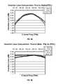
- FIGS. 9 a and 9 bshow the insertion loss over a portion of the C-band for an illustrative optical processing device without compensation for the wavelength dependence on the angle of diffraction from the DMD and with compensation for the wavelength dependence on the angle of diffraction, respectively.
- FIG. 1shows a simplified example of a wavelength blocker 100 that is based on a MEMs mirror array 108 such as a DMD.
- the fiber array 110is a single fiber that serves as an input and output port.
- a circulator(not shown) or other means are used to separate the incoming and outgoing beams.
- the fiber arrayincludes N fibers, then each fiber serves as an input and output port.
- Such a deviceprovides N 1 ⁇ 1 wavelength blockers using a common optical fabric and is referred to as a wavelength blocker array.
- the launch opticswould generally require the fiber array and a series of circulators or the like to separate each of the N incoming beams and the N outgoing beams.
- FIG. 2Another example of an optical processing device is shown in FIG. 2 .
- Ne.g., 15
- the launch optics arrangement 260includes a fiber array 250 in combination with a lenslet array 200 .
- the fiber array 250typically consists of two V-groove plates that secure the input/output fibers.
- FIG. 2shows two fiber pairs; pair one includes fibers 1 and 2 and pair two includes fibers 3 and 4 .
- the launch optics arrangement 260 shown in FIG. 2includes a fiber array
- the launch optics arrangement 260may include any type of waveguide array such as a planar waveguide array, for example.
- the waveguides employed in the arraymay all be of the same type or a combination of different types (e.g., fiber and planar).
- the lenslet array 200includes inner and outer opposing surfaces 220 and 230 and is formed from silica or another suitably optically transparent material.
- a series of collimating lens pairs 210 1 , 210 2are arranged on the inner surface 220 of the lenslet array 200 .
- Each collimating lens pair 210includes two collimating lenses 212 .
- a series of coupling lens 214 1 , 214 2are formed on the outer surface 230 of the lenslet array 200 .
- Each collimating lens pair 210is in registration with one of the coupling lens 214 .
- collimating lens pair 210 1is in registration with coupling lens 214 1
- collimating lens pair 210 2is in registration with coupling lens 214 2 .
- the pitch of the collimating lenses 212is the same as the pitch of the fibers in the fiber array 250 . Accordingly, the fiber array 250 and the lenslet array 200 are arranged so that each of the collimating lenses 212 of the lenslet array 200 is in registration with one of the fiber outputs in the fiber array 250 . In some particular implementations the separation between the collimating lenses 212 and the coupling lenses 214 may be about equal to the sum of their individual focal lengths.
- the operation of the launch optics arrangement 260 in FIG. 2is as follows.
- a light beam from an input fiber in each fiber pairis communicated from the fiber array 250 into the lenslet array 200 through the collimating lens 212 with which it is registration.
- light from fiber 1is shown entering its corresponding collimating lens 212 in collimating lens pair 210 1 .
- the collimating lens 212directs a collimated beam to the coupling lens 214 with which it is in registration.
- the collimated beam from fiber 1is collimated by collimating lens 212 in collimating lens pair 210 1 , which directs the collimated beam to coupling lens 214 1 .
- the coupling lens 214focuses the beam in a launch plane, where, in the example shown in FIG. 2 , a coupling mirror 240 is located.
- the coupling mirror 240reflects the beam so that it is directed back through the same coupling lens from which it was received (e.g., coupling lens 214 1 in FIG. 2 ).
- the coupling lens 214collimates the reflected beam and directs it back through the lenslet array 200 . Because of the angle through which the beam was reflected by the coupling mirror 240 , the reflected collimated beam is parallel to and spatially offset from the incoming collimated beam.
- the reflected collimated beamis directed to the output collimating lens of the collimating lens pair that initially received the beam from fiber array 250 .
- the beam directed into the lenslet array 200 through the input collimating lens 212 of collimating lens pair 210 1is directed to the adjacent output collimating lens 212 in collimating lens pair 210 1 .
- the output collimating lens 212focuses the reflected beam onto the input of the fiber in registration with the output collimating lens 212 , which in the example shown in FIG. 2 is fiber 2 .
- the optical processing device shown in FIG. 2directs an input beam received from one fiber (e.g., fiber 1 ) in a fiber pair to another fiber (e.g., fiber 2 ) in the same fiber pair, thus providing a switching function.
- This exampleemploys the same optical launch arrangement as shown in FIG. 2 , but replaces the coupling mirror 240 with an optical system that includes a DMD 550 , In this particular example, N 1 ⁇ 1 wavelength blockers are formed. If, for instance, the optical processing device includes 15 1 ⁇ 1 wavelength blockers (only three of which are shown in FIG. 3 ), fiber array 505 would include 30 input/output fibers.
- the optical launch arrangement 570is followed by collimating lens 516 , diffraction gratings 522 , scan lens 530 , compensating prism 540 and DMD 550 .
- the DMD 550is tilted with respect to the optical axis of the scan lens 530 in a plane in which the fibers of the launch optics arrangement 570 extend.
- an optical beam entering the optical launch arrangement 570 from a fiber 502exits the corresponding collimating lens 514 and comes to a virtual focus in the launch plane 511 .
- the optical beamis then collimated by a collimating lens 516 .
- the diffraction grating 522next diffracts the collimated beam and the scan lens 530 focuses the spectrally dispersed beams onto the DMD 550 after passing through the compensating prism 540 .
- the individual mirrors of the DMD 550are tilted to reflect the beam nearly back on itself (near Littrow) so that it travels back through the device and exits through the corresponding waveguide 504 of the launch optics arrangement 570 .
- FIG. 3shows the operation for only the coupled fiber pair 502 and 504 , the coupling described above occurs for all of the fiber pairs.
- the distance from the scan lens 530 to the DMD 550varies from fiber to fiber.
- the function of the compensating prism 540is to correct for this path length difference so that the beams from all the fibers are focused on the DMD 550 .
- the operation of the compensating prism 540can be more easily seen in FIG. 4 , which shows the relationship between the compensating prism 540 and the DMD 550 , which may include a transparent window 420 .
- the device shown in FIG. 3has an inherent wavelength dependent loss which limits its performance.
- the DMD 550is composed of an array of micro mirrors and thus behaves as a diffraction grating rather than a mirror. Strictly speaking, the beams are diffracted off of the DMD, not reflected.
- the angle of diffraction from the DMD 550 in the plane of the fiber array 505is given by the grating equation, which shows that the angle of diffraction of the beams from the DMD is wavelength dependent.
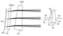
- FIG. 5shows two beams, a short wavelength beam 370 and a long wavelength beam 380 , as they pass through the compensating prism 540 and diffract off of the DMD 550 .
- the long wavelength beam 380diffracts through a larger angle compared to the short wavelength beam 370 .
- FIGS. 6 a and 6 bshow the short wavelength beam 370 (solid line) being diffracted from DMD 550 .
- FIG. 6 aalso shows the diffraction angle ⁇ d though which the beam 370 is diffracted.
- FIG. 6 bsimilarly shows the long wavelength beam 380 (solid line) being diffracted from DMD 550 .
- FIG. 6 balso shows the diffraction angle ⁇ d though which the beam 380 is diffracted.
- Comparison of FIGS. 6 a and 6 bshows that the longer wavelength beam 380 diffracts through the larger angle.
- the wavelength dependent losscan be minimized or eliminated by providing a suitable optical element to compensate for the wavelength dependence of the diffracted angle which is introduced by diffraction from the DMD.
- this optical elementshould be located downstream from the diffraction grating 522 in FIG. 3 , typically in the vicinity of the DMD 550 . That is, the optical element may be located between the diffraction grating 522 and the DMD 550 .
- an existing optical elementmay be modified to perform this function.
- the shape of the compensating prism 540 in FIG. 3may be modified to correct for this loss. In this case the compensating prism 540 both adjusts the path length difference experienced by the beams from each fiber and compensates for wavelength dependent loss arising from DMD diffraction.
- a slight twistmay be added to one or both of the surfaces of the compensating prism 540 .
- FIG. 7for the incoming surface 394 of compensating prism 385 .
- the surface 394causes the long wavelength beam 392 to be refracted at a greater angle of refraction than the short wavelength beam 390 .
- the shape of such a surfaceis shown in FIG. 8 .
- the correction for the wavelength dependent losscan also be achieved by adding cylindrical surfaces to each surface of the compensating prism 385 .
- One advantage of this approachis that a cylindrical surface can be generated using conventional optical polishing methods.
- the DMD 550 , window 420 and compensating prism 540may be packaged in a single unit to provide a DMD arrangement that diffracts an optical beam in a wavelength-independent manner.
- a DMD arrangementwhich may be used in a wide variety of different optical processing devices.
- FIGS. 9 a and 9 bshow the insertion loss over a portion of the C-band for an illustrative optical processing device without compensation for the wavelength dependence on the angle of diffraction from the DMD and with compensation for the wavelength dependence on the angle of diffraction, respectively. As shown, the amount of loss and the variation in loss is reduced when the wavelength dependence is reduced.
Landscapes
- Physics & Mathematics (AREA)
- General Physics & Mathematics (AREA)
- Optics & Photonics (AREA)
- Engineering & Computer Science (AREA)
- Computer Networks & Wireless Communication (AREA)
- Mechanical Light Control Or Optical Switches (AREA)
- Optical Couplings Of Light Guides (AREA)
Abstract
Description
Claims (23)
Priority Applications (8)
| Application Number | Priority Date | Filing Date | Title |
|---|---|---|---|
| US13/325,555US8681422B2 (en) | 2011-12-14 | 2011-12-14 | Optical processing device employing a digital micromirror device (DMD) and having reduced wavelength dependent loss |
| CA2798382ACA2798382A1 (en) | 2011-12-14 | 2012-12-13 | Optical processing device employing a digital micromirror device (dmd) and having reduced wavelength dependent loss |
| JP2012272107AJP6172928B2 (en) | 2011-12-14 | 2012-12-13 | Optical processing device using a digital micromirror device (DMD) with reduced wavelength dependent loss |
| EP12008333.2AEP2605051B1 (en) | 2011-12-14 | 2012-12-14 | Optical processing device employing a digital micromirror device (dmd) and having reduced wavelength dependent loss |
| AU2012261755AAU2012261755B2 (en) | 2011-12-14 | 2012-12-14 | Optical processing device employing a digital micromirror (DMD) and having reduced wavelength dependent loss |
| BRBR102012032078-9ABR102012032078A2 (en) | 2011-12-14 | 2012-12-14 | Optical Arrangement, Optical Processing Device, and Method for Processing an Optical Signal |
| KR1020120145999AKR101958395B1 (en) | 2011-12-14 | 2012-12-14 | Optical processing device employing a digital micromirror device(dmd) and having reduced wavelength dependent loss |
| CN201210599134.0ACN103163642B (en) | 2011-12-14 | 2012-12-14 | Using DMD (DMD) and with the optical treatment equipment of the wavelength associated loss reduced |
Applications Claiming Priority (1)
| Application Number | Priority Date | Filing Date | Title |
|---|---|---|---|
| US13/325,555US8681422B2 (en) | 2011-12-14 | 2011-12-14 | Optical processing device employing a digital micromirror device (DMD) and having reduced wavelength dependent loss |
Publications (2)
| Publication Number | Publication Date |
|---|---|
| US20130155512A1 US20130155512A1 (en) | 2013-06-20 |
| US8681422B2true US8681422B2 (en) | 2014-03-25 |
Family
ID=47562918
Family Applications (1)
| Application Number | Title | Priority Date | Filing Date |
|---|---|---|---|
| US13/325,555Active2031-12-28US8681422B2 (en) | 2011-12-14 | 2011-12-14 | Optical processing device employing a digital micromirror device (DMD) and having reduced wavelength dependent loss |
Country Status (8)
| Country | Link |
|---|---|
| US (1) | US8681422B2 (en) |
| EP (1) | EP2605051B1 (en) |
| JP (1) | JP6172928B2 (en) |
| KR (1) | KR101958395B1 (en) |
| CN (1) | CN103163642B (en) |
| AU (1) | AU2012261755B2 (en) |
| BR (1) | BR102012032078A2 (en) |
| CA (1) | CA2798382A1 (en) |
Cited By (1)
| Publication number | Priority date | Publication date | Assignee | Title |
|---|---|---|---|---|
| US11201673B1 (en)* | 2018-03-07 | 2021-12-14 | BridgeSat, Inc. | Optical laser communication apparatus with optical phased arrays and coupling arrangement and associated methods |
Families Citing this family (6)
| Publication number | Priority date | Publication date | Assignee | Title |
|---|---|---|---|---|
| JP6322926B2 (en)* | 2013-08-12 | 2018-05-16 | 大日本印刷株式会社 | Illumination device, projection device, and projection display device |
| JP6251202B2 (en)* | 2015-01-27 | 2017-12-20 | 日本電信電話株式会社 | Wavelength selective switch |
| US10228517B2 (en)* | 2015-03-03 | 2019-03-12 | Nistica, Inc. | Optical arrangement for managing diversity and isolation between ports in a wavelength selective switch |
| CN107462987B (en)* | 2016-06-02 | 2019-12-03 | 苏州旭创科技有限公司 | Light path control system and optical module |
| CN106918932A (en)* | 2017-03-09 | 2017-07-04 | 苏州晶萃光学科技有限公司 | A kind of optically controlled liquid crystal spatial light modulator and its application |
| US11561345B2 (en)* | 2020-02-14 | 2023-01-24 | Google Llc | Apertures for reduced dynamic crosstalk and stray light control |
Citations (10)
| Publication number | Priority date | Publication date | Assignee | Title |
|---|---|---|---|---|
| US20010035939A1 (en)* | 2000-03-28 | 2001-11-01 | Toshifumi Mihashi | Eye characteristic measuring apparatus |
| US20020079432A1 (en) | 2000-08-07 | 2002-06-27 | Lee Benjamin L. | Two-dimensional blazed MEMS grating |
| US20020176151A1 (en) | 2001-04-03 | 2002-11-28 | John Moon | Dynamic optical filter having a spatial light modulator |
| US20020181858A1 (en)* | 2000-02-17 | 2002-12-05 | Oleg Bouevitch | Wavelength switch with independent channel equalization |
| US6760501B2 (en)* | 2000-12-05 | 2004-07-06 | Jds Uniphase Inc. | Device for imposing a field tilt for approximating the inherent field curvature of a focusing element in a free space optical device |
| US6956687B2 (en)* | 2001-04-03 | 2005-10-18 | Cidra Corporation | Optical blocking filter having an array of micro-mirrors |
| US20060159395A1 (en)* | 2004-04-20 | 2006-07-20 | Alan Hnatiw | Optical compensator array for dispersive element arrays |
| US20070299487A1 (en)* | 2003-03-06 | 2007-12-27 | Shadduck John H | Adaptive Optic Lens and Method of Making |
| US7639906B1 (en)* | 2004-04-23 | 2009-12-29 | Nistica, Inc. | Tunable optical communication system |
| US20100103498A1 (en) | 2008-10-24 | 2010-04-29 | Texas Instruments Incorporated | Digital micromirror device having wavelength-dependent modulation structure and method of manufacturing the same |
Family Cites Families (9)
| Publication number | Priority date | Publication date | Assignee | Title |
|---|---|---|---|---|
| US6449033B2 (en)* | 1999-04-26 | 2002-09-10 | Corning Incorporated | Apparatus and method for measuring polarization dependent loss |
| US6618520B2 (en)* | 1999-11-09 | 2003-09-09 | Texas Instruments Incorporated | Micromirror optical switch |
| KR100805969B1 (en)* | 2000-09-29 | 2008-02-25 | 텍사스 인스트루먼츠 인코포레이티드 | Optical add drop multiplexer |
| US6885807B2 (en) | 2001-03-14 | 2005-04-26 | Nuonics, Inc. | High speed fiber-optic attenuation modules |
| US6934069B2 (en) | 2001-04-03 | 2005-08-23 | Cidra Corporation | Chromatic dispersion compensation device having an array of micromirrors |
| US7397986B2 (en)* | 2005-03-04 | 2008-07-08 | Gemfire Corporation | Optical device with reduced temperature dependence |
| JP2006276216A (en)* | 2005-03-28 | 2006-10-12 | Fujitsu Ltd | Light switch |
| DE102007011561B4 (en)* | 2007-03-02 | 2016-03-17 | Seereal Technologies S.A. | Device for correcting the wavelength dependence in diffraction-based optical systems |
| US8086080B2 (en)* | 2007-07-23 | 2011-12-27 | Nistica, Inc. | Multiple function digital optical switch |
- 2011
- 2011-12-14USUS13/325,555patent/US8681422B2/enactiveActive
- 2012
- 2012-12-13JPJP2012272107Apatent/JP6172928B2/enactiveActive
- 2012-12-13CACA2798382Apatent/CA2798382A1/ennot_activeAbandoned
- 2012-12-14EPEP12008333.2Apatent/EP2605051B1/enactiveActive
- 2012-12-14AUAU2012261755Apatent/AU2012261755B2/ennot_activeCeased
- 2012-12-14KRKR1020120145999Apatent/KR101958395B1/enactiveActive
- 2012-12-14BRBRBR102012032078-9Apatent/BR102012032078A2/ennot_activeApplication Discontinuation
- 2012-12-14CNCN201210599134.0Apatent/CN103163642B/enactiveActive
Patent Citations (10)
| Publication number | Priority date | Publication date | Assignee | Title |
|---|---|---|---|---|
| US20020181858A1 (en)* | 2000-02-17 | 2002-12-05 | Oleg Bouevitch | Wavelength switch with independent channel equalization |
| US20010035939A1 (en)* | 2000-03-28 | 2001-11-01 | Toshifumi Mihashi | Eye characteristic measuring apparatus |
| US20020079432A1 (en) | 2000-08-07 | 2002-06-27 | Lee Benjamin L. | Two-dimensional blazed MEMS grating |
| US6760501B2 (en)* | 2000-12-05 | 2004-07-06 | Jds Uniphase Inc. | Device for imposing a field tilt for approximating the inherent field curvature of a focusing element in a free space optical device |
| US20020176151A1 (en) | 2001-04-03 | 2002-11-28 | John Moon | Dynamic optical filter having a spatial light modulator |
| US6956687B2 (en)* | 2001-04-03 | 2005-10-18 | Cidra Corporation | Optical blocking filter having an array of micro-mirrors |
| US20070299487A1 (en)* | 2003-03-06 | 2007-12-27 | Shadduck John H | Adaptive Optic Lens and Method of Making |
| US20060159395A1 (en)* | 2004-04-20 | 2006-07-20 | Alan Hnatiw | Optical compensator array for dispersive element arrays |
| US7639906B1 (en)* | 2004-04-23 | 2009-12-29 | Nistica, Inc. | Tunable optical communication system |
| US20100103498A1 (en) | 2008-10-24 | 2010-04-29 | Texas Instruments Incorporated | Digital micromirror device having wavelength-dependent modulation structure and method of manufacturing the same |
Non-Patent Citations (6)
| Title |
|---|
| Fastie, "A Small Plane Grating Monochromator", Journal of the Optical Society of America, vol. 42 No. 9, p. 641-647, Sep. 1952.* |
| Khan et al. ("Demonstration of the MEMS Digital Micromirror Device-Based Broadband Reconfigurable Optical Add-Drop Filter for Dense Wavelength-Division-Multiplexing Systems," Lightwave Technology, Journal of, vol. 25, No. 2, pp. 520-526, Feb. 2007).* |
| Nabeel A. Riza et al. "Broadband Optical Equalizer Using Fault-Tolerant Digital Micromirrors", Optics Express, vol. 11, No. 13, Jun. 30, 2003, pp. 1559-1565. |
| Riza N. A. et al., "Broadband All-Digital Variable Fiber-Optic Attenuator Using Digital Micromirror Device" IEEE Photonics Technology Letters, vol. 19, No. 21, Nov. 1, 2007, pp. 1705-1707. |
| Sakurai et al. ("LCOS-Based Wavelength Blocker Array With Channel-by-Channel Variable Center Wavelength and Bandwidth," Photonics Technology Letters, IEEE , vol. 23, No. 14, pp. 989,991, Jul. 2011).* |
| Yoder et al. "DLP Technology Applicaitons in Optical Networking" Proceedings of SPIE, vol. 4457, Nov. 8, 2001, pp. 54-61. |
Cited By (3)
| Publication number | Priority date | Publication date | Assignee | Title |
|---|---|---|---|---|
| US11201673B1 (en)* | 2018-03-07 | 2021-12-14 | BridgeSat, Inc. | Optical laser communication apparatus with optical phased arrays and coupling arrangement and associated methods |
| US20220263575A1 (en)* | 2018-03-07 | 2022-08-18 | Bridgecomm, Inc. | Optical laser communication apparatus with optical phased arrays and coupling arrangement and associated methods |
| US11967989B2 (en)* | 2018-03-07 | 2024-04-23 | Bridgecomm, Inc. | Optical laser communication apparatus with optical phased arrays and coupling arrangement and associated methods |
Also Published As
| Publication number | Publication date |
|---|---|
| EP2605051B1 (en) | 2019-10-30 |
| KR20130069480A (en) | 2013-06-26 |
| US20130155512A1 (en) | 2013-06-20 |
| JP2013125278A (en) | 2013-06-24 |
| JP6172928B2 (en) | 2017-08-02 |
| EP2605051A1 (en) | 2013-06-19 |
| AU2012261755B2 (en) | 2015-04-30 |
| CN103163642A (en) | 2013-06-19 |
| CN103163642B (en) | 2018-04-03 |
| CA2798382A1 (en) | 2013-06-14 |
| BR102012032078A2 (en) | 2015-04-14 |
| KR101958395B1 (en) | 2019-03-14 |
| AU2012261755A1 (en) | 2013-07-11 |
Similar Documents
| Publication | Publication Date | Title |
|---|---|---|
| US8681422B2 (en) | Optical processing device employing a digital micromirror device (DMD) and having reduced wavelength dependent loss | |
| AU2012216378B2 (en) | Asymmetric lenslet array | |
| US7725027B2 (en) | Multi-unit wavelength dispersive device | |
| US7302133B2 (en) | Optical switch | |
| US7630599B2 (en) | Wavelength dispersive device with temperature compensation | |
| JP4967847B2 (en) | Optical switch and MEMS package | |
| US20030095307A1 (en) | Reconfigurable optical add/drop multiplexer having an array of micro-mirrors | |
| US20080239441A1 (en) | Mirror device and optical apparatus | |
| US8693818B2 (en) | Optical processing device | |
| US6766081B2 (en) | Focal length dispersion compensation for field curvature | |
| US7333686B1 (en) | System and method for a re-configurable optical channel dropping de-multiplexer | |
| US7277607B2 (en) | Optical multiplexer/demultiplexer, optical device, and optical transmission system | |
| EP2570829B1 (en) | Optical processing device |
Legal Events
| Date | Code | Title | Description |
|---|---|---|---|
| AS | Assignment | Owner name:NISTICA, INC., NEW JERSEY Free format text:ASSIGNMENT OF ASSIGNORS INTEREST;ASSIGNORS:HALLER, MITCHELL E.;WAGENER, JEFFERSON L.;REEL/FRAME:027961/0539 Effective date:20120301 | |
| STCF | Information on status: patent grant | Free format text:PATENTED CASE | |
| MAFP | Maintenance fee payment | Free format text:PAYMENT OF MAINTENANCE FEE, 4TH YR, SMALL ENTITY (ORIGINAL EVENT CODE: M2551) Year of fee payment:4 | |
| AS | Assignment | Owner name:MOLEX, LLC, ILLINOIS Free format text:ASSIGNMENT OF ASSIGNORS INTEREST;ASSIGNOR:AFL TELECOMMUNICATIONS, INC.;REEL/FRAME:054117/0554 Effective date:20180921 Owner name:AFL TELECOMMUNICATIONS, INC., NEW JERSEY Free format text:CHANGE OF NAME;ASSIGNOR:NISTICA, INC.;REEL/FRAME:054157/0531 Effective date:20180306 | |
| FEPP | Fee payment procedure | Free format text:ENTITY STATUS SET TO UNDISCOUNTED (ORIGINAL EVENT CODE: BIG.); ENTITY STATUS OF PATENT OWNER: LARGE ENTITY | |
| MAFP | Maintenance fee payment | Free format text:PAYMENT OF MAINTENANCE FEE UNDER 1.28(C) (ORIGINAL EVENT CODE: M1559); ENTITY STATUS OF PATENT OWNER: LARGE ENTITY | |
| MAFP | Maintenance fee payment | Free format text:PAYMENT OF MAINTENANCE FEE, 8TH YEAR, LARGE ENTITY (ORIGINAL EVENT CODE: M1552); ENTITY STATUS OF PATENT OWNER: LARGE ENTITY Year of fee payment:8 | |
| FEPP | Fee payment procedure | Free format text:PETITION RELATED TO MAINTENANCE FEES GRANTED (ORIGINAL EVENT CODE: PTGR); ENTITY STATUS OF PATENT OWNER: LARGE ENTITY | |
| MAFP | Maintenance fee payment | Free format text:PAYMENT OF MAINTENANCE FEE, 12TH YEAR, LARGE ENTITY (ORIGINAL EVENT CODE: M1553); ENTITY STATUS OF PATENT OWNER: LARGE ENTITY Year of fee payment:12 |