US8680884B2 - Fault detection circuits for switched mode power supplies and related methods of operation - Google Patents
Fault detection circuits for switched mode power supplies and related methods of operationDownload PDFInfo
- Publication number
- US8680884B2 US8680884B2US12/756,573US75657310AUS8680884B2US 8680884 B2US8680884 B2US 8680884B2US 75657310 AUS75657310 AUS 75657310AUS 8680884 B2US8680884 B2US 8680884B2
- Authority
- US
- United States
- Prior art keywords
- signal
- circuit
- duty cycle
- fault
- gate drive
- Prior art date
- Legal status (The legal status is an assumption and is not a legal conclusion. Google has not performed a legal analysis and makes no representation as to the accuracy of the status listed.)
- Active, expires
Links
Images


Classifications
- G—PHYSICS
- G01—MEASURING; TESTING
- G01R—MEASURING ELECTRIC VARIABLES; MEASURING MAGNETIC VARIABLES
- G01R31/00—Arrangements for testing electric properties; Arrangements for locating electric faults; Arrangements for electrical testing characterised by what is being tested not provided for elsewhere
- G01R31/40—Testing power supplies
- H—ELECTRICITY
- H05—ELECTRIC TECHNIQUES NOT OTHERWISE PROVIDED FOR
- H05B—ELECTRIC HEATING; ELECTRIC LIGHT SOURCES NOT OTHERWISE PROVIDED FOR; CIRCUIT ARRANGEMENTS FOR ELECTRIC LIGHT SOURCES, IN GENERAL
- H05B45/00—Circuit arrangements for operating light-emitting diodes [LED]
- H05B45/50—Circuit arrangements for operating light-emitting diodes [LED] responsive to malfunctions or undesirable behaviour of LEDs; responsive to LED life; Protective circuits
- H—ELECTRICITY
- H02—GENERATION; CONVERSION OR DISTRIBUTION OF ELECTRIC POWER
- H02M—APPARATUS FOR CONVERSION BETWEEN AC AND AC, BETWEEN AC AND DC, OR BETWEEN DC AND DC, AND FOR USE WITH MAINS OR SIMILAR POWER SUPPLY SYSTEMS; CONVERSION OF DC OR AC INPUT POWER INTO SURGE OUTPUT POWER; CONTROL OR REGULATION THEREOF
- H02M1/00—Details of apparatus for conversion
- H02M1/32—Means for protecting converters other than automatic disconnection
Definitions
- the present inventionrelates to power conversion and, more particularly, to power supply circuits and related methods of operation.
- Power converter circuitsmay be used to convey power from a source, such as a battery, electrical power grid, etc. to a load, such as any device, apparatus, or component that runs on electricity, preferably with as little loss as possible.
- a power converter circuitprovides an output voltage that has a different level than the input voltage.
- One type of power converter circuitis known as a switching or switched mode power supply.
- a switched mode power supplycontrols the flow of power from a power source to a load by controlling the “on” and “off” duty cycle of one or more transistor switches in order to regulate the DC output voltage across the output terminals of the power supply.
- the “on” and “off” duty cycle of the one or more transistor switchesmay be controlled in response to a pulse-width-modulated (PWM) gate drive signal provided by a switching regulator circuit, such that the “on” and “off” duty cycle of the one or more transistor switches is determined by relative pulse-widths of the PWM signal.
- PWMpulse-width-modulated
- Some switched mode power suppliesmay use a transformer or an inductor as an energy transfer element.
- a power transistormay be coupled to one side of the primary winding of a transformer, and may be turned on and off in response to the gate drive signal provided by the switching regulator circuit to alternately store energy in the magnetic field of the transformer and transfer the stored energy to the secondary winding.
- the secondary winding of the transformermay develop a rectified output voltage across a shunt capacitor coupled across the secondary winding as a function of the energy transfer. The voltage across the capacitor may provide the DC output voltage of the switching power supply.
- the DC output voltage, or a representation thereof,may be fed back to the switching regulator circuit to allow the switched mode power supply to compensate for load variation.
- the DC output voltagedecreases, which may cause the switching regulator to alter the gate drive signal to leave the power transistor “on” for a longer average period of time in order to store more energy in the magnetic field.
- the additional energymay be transferred to the secondary winding during the “off” time of the power transistor to supply the increased load and re-establish the DC output voltage.
- the DC output voltageincreases, which may cause the switching regulator to alter the gate drive signal to leave the power transistor “on” for a shorter average period of time to store less energy in the magnetic field.
- the reduced energy transfer to the secondary winding during the “off” time of the power transistormay cause the power supply to adjust to the decreased load and may reduce the DC output voltage back to its steady-state value.
- Switched mode power supplieshave been implemented as an efficient mechanism for providing a regulated output, and are generally more power efficient than linear voltage regulators, which dissipate unwanted power as heat.
- many switched mode power suppliesmay not be able to detect overload or fault conditions. Examples of possible faults may include a short-circuit or open-circuit at the output of the power supply, broken or unpopulated magnetic components, and/or loss of power to be converted at the input of the power supply.
- a circuit for detecting fault conditions in a supply circuitincludes a monitoring circuit and a comparator circuit.
- the monitoring circuitis operable to output a detection signal related to a characteristic of a control signal for the supply circuit.
- the comparator circuitis operable to compare the detection signal to a range defined by first and second thresholds and output a fault signal according to a relationship of the detection signal to the range over a time period.
- the supply circuitmay be a switched mode power supply
- the control signalmay be configured to operate at least one switch of the supply circuit between alternating activated and deactivated states, for example, to provide power to a load.
- the detection signalmay be indicative of a characteristic of the control signal.
- the characteristic of the control signalmay be a duty cycle of the control signal, the first threshold may represent an upper limit for the duty cycle, and the second threshold may represent a lower limit for the duty cycle.
- the characteristic of the control signalmay be a frequency of the control signal, the first threshold may represent an upper limit for the frequency, and the second threshold may represent a lower limit for the frequency.
- the comparatormay be operable to output the fault signal when the detection signal is not within the range defined between the first and second thresholds for the time period.
- the at least one switchmay be a power transistor, and the control signal may be a gate drive signal for the power transistor.
- the monitoring circuitmay include an averaging circuit that is operable to receive the gate drive signal, determine an average value representing the gate drive signal based on the duty cycle thereof, and output the average value to the comparator circuit as the detection signal indicative of the duty cycle.
- the first thresholdmay be an average value representing the gate drive signal at a maximum duty cycle
- the second thresholdmay be an average value representing the gate drive signal at a minimum duty cycle
- the circuitmay further include a logic circuit that is operable to receive respective gate drive signals from a plurality of switched mode power supply controllers.
- the logic circuitmay be operable to output a first signal representing one of the respective gate drive signals having a longest duty cycle and a second signal representing one of the respective gate drive signals having a shortest duty cycle to the averaging circuit.
- the averaging circuitmay be operable to output a first average value representing the one of the respective gate drive signals having the longest duty cycle and a second average value representing the one of the respective gate drive signals having the shortest duty cycle.
- the comparator circuitmay be operable to compare the first average value to the first threshold, to compare the second average value to the second threshold, and to output the fault signal when the first average value is greater than or equal to the first threshold and/or when the second average value is less than or equal to the second threshold.
- the comparator circuitmay include first and second comparators.
- the first comparatormay be operable to compare the detection signal indicative of the duty cycle of the control signal to the first threshold and output the fault signal when the detection signal is greater than or equal to the first threshold.
- the second comparatormay be operable to compare the detection signal indicative of the duty cycle of the control signal to the second threshold an output the fault signal when the detection signal is less than or equal to the second threshold.
- the fault signalmay include a first fault signal indicating an open-circuit condition and a second fault signal indicating a short-circuit condition.
- the first comparatormay be operable to output the first fault signal when the detection signal indicative of the duty cycle is greater than or equal to the first threshold
- the second comparatormay be operable to output the second fault signal when the detection signal indicative of the duty cycle is less than or equal to the second threshold.
- the comparator circuitmay be operable to output a power-good signal indicating that no fault conditions exist when the detection signal indicative of the duty cycle is less than the first threshold and is greater than the second threshold.
- the monitoring circuitmay be operable to output the detection signal responsive to receiving the control signal from a controller of the supply circuit. In other embodiments, the monitoring circuit may be operable to output the detection signal responsive to a feedback signal from a load connected to the supply circuit.
- the circuitmay further include a decoupling circuit operable to decouple the supply circuit from a power source in response to the fault signal.
- a method of detecting fault conditions in a supply circuitincludes generating a detection signal related to a control signal for the supply circuit.
- the detection signalis compared to a range defined by first and second thresholds, and a fault signal is provided when the detection signal is not within the range defined by the first and second thresholds for a period of time.
- the supply circuitmay be a switched mode power supply
- the control signalmay be configured to drive at least one switching element of the supply circuit between alternating activated and deactivated states to supply power to a load.
- the detection signalmay be indicative of a characteristic of the control signal.
- the characteristic of the control signalmay be a duty cycle of a control signal, an amplitude of the control signal and/or a frequency of the control signal.
- the detection signalmay indicate a sampled value for the characteristic, an average value for the characteristic, and/or a rate of change for the characteristic, and the range may be an operating range for the characteristic.
- the at least one switching elementmay be a power transistor
- the control signalmay be a gate drive signal for the power transistor
- the characteristic of the control signalmay be a duty cycle of the gate drive signal
- an average value representing the gate drive signalmay be determined based on the duty cycle of the gate drive signal.
- the average valuemay be output as the detection signal indicative of the duty cycle of the gate drive signal, and the average value may be compared to the first and second thresholds.
- the first thresholdmay be an average value representing the gate drive signal at an upper limit of the duty cycle
- the second thresholdmay be an average value representing the gate drive signal at a lower limit of the duty cycle.
- providing the fault signalmay include providing a first fault signal indicating an open-circuit condition when the detection signal indicative of the duty cycle of the gate drive signal is greater than or equal to the first threshold, and providing a second fault signal indicating a short-circuit condition when the detection signal indicative of the duty cycle of the gate drive signal is less than or equal to the second threshold.
- a power-good signal indicating that no fault conditions existmay be provided when the detection signal indicative of the duty cycle is less than the first threshold and is greater than the second threshold.
- a feedback signalmay be received from a load connected to the supply circuit, and the detection signal may be generated responsive to receiving the feedback signal.
- a switched mode power supplyincludes at least one switching element operable to be switched between alternating activated and deactivated states to supply power to a load, and a controller circuit operable to output a control signal to the at least one switching element.
- the control signalis configured to drive the at least one switching element between the alternating activated and deactivated states.
- the switched mode power supplyfurther includes a first circuit and a second circuit.
- the first circuitis coupled to the controller and is operable to output a signal indicative of a duty cycle of the control signal.
- the second circuitis coupled to the first circuit and is operable to compare the signal indicative of the duty cycle of the control signal to a range defined by first and second thresholds.
- the second circuitis further operable to output a fault signal when the signal indicative of the duty cycle of the control signal falls outside of the range defined by the first and second thresholds for a predetermined amount of time.
- FIG. 1is a block diagram illustrating a power converter circuit including a fault detection circuit according to some embodiments of the present invention.
- FIG. 2is a block diagram illustrating the fault detection circuit of FIG. 1 in greater detail.
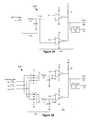
- FIGS. 3A and 3Bare schematic diagrams illustrating fault detection circuits according to some embodiments of the present invention.
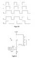
- FIG. 3Cis a timing diagram illustrating the relative on-times for the gate drive signals illustrated in FIG. 3B .
- FIG. 4is a schematic diagram illustrating a buck converter circuit that may be used with fault detection circuits according to some embodiments of the present invention.
- FIGS. 5 and 6are flowcharts illustrating example operations performed by fault detection circuits according to some embodiments of the present invention.
- switched mode power supply controllersmay not typically be designed to detect fault conditions, characteristics of a control signal of a switching device of the power supply, such as, for example, the duty cycle of the gate drive signal, may change when certain types of faults occur.
- embodiments of the present inventionmonitor one or more characteristics or parameters of a control signal of a switching element in a switched mode power supply to detect faults in the switched mode power supply.
- the characteristic(s) of the control signalmay be directly or indirectly measured.
- a range and/or thresholdmay be established for the measure of the control signal and a fault detected based on a relationship of the measure and the range and/or threshold.
- the range and/or thresholdmay reflect normal operation or the range and/or the threshold may reflect a fault in the power supply. Thus, for example, if a range reflects normal operation and the measure is within the range, then no fault is detected. If the measure falls outside of the range, then a fault is detected.
- a fault signal or a no-fault/good signalmay be generated based on the relationship of the measure of the characteristic of the control signal and the range and/or threshold.
- the measure of the control signalmay be an analog or digital value and may be continuous or discrete.
- the characteristic of the control signal that is measuredmay depend on the specific design of the switched mode power supply.
- the characteristicmay be the duty cycle of a control signal, an amplitude of a control signal and/or a frequency of a control signal.
- the measuremay be a sampled value for the characteristic, an average value for the characteristic, a rate of change for the characteristic, a convolution with the characteristic, or combinations thereof.
- FIG. 1is a block diagram illustrating a power converter circuit 100 including a fault detection circuit 105 according to some embodiments of the present invention.
- the power converter circuit 100includes a supply circuit, shown as switched mode power supply (SMPS) 120 , that connects a power source 110 to a load 130 .
- the power source 110may be an Alternating Current (AC) or a Direct Current (DC) power source.
- the SMPS 120includes a switching element or switch 140 , a rectifier component 150 , a storage component 160 , and a fault detection component 105 .
- the load 130may be any apparatus or device that receives the output voltage/current generated by the SMPS 120 responsive to an input voltage/current received from the power source 110 .
- the storage component 160may include a magnetic field storage component (such as an inductor and/or a transformer) and/or an electric field storage component (such as a capacitor).
- the SMPS 120may, in some embodiments, be a DC to DC power converter.
- the DC to DC power converter circuitmay be configured in, for example but not limited to, a buck configuration, a boost configuration, and a buck-boost configuration.
- the SMPS 120may be an AC to DC, AC to AC, or DC to AC power converter in other embodiments.
- the fault detection component 105may be separate from and/or external to the SMPS 120 in some embodiments.
- the switch 140may be operable to provide alternating activated and deactivated states, such as closed and open states, on and off states, etc., to supply power to the load 130 .
- the rectifier component 150may be biased in at least two operational states, such as forward or reverse biased. When the switch 140 is in the “on” or “closed” operational state, the rectifier component 150 is in a first bias state and energy from the power source 110 is stored in the storage component 160 . When the switch 140 transitions to the “off” or “open” operational state, the rectifier component 150 is in a second bias state and the energy stored in the storage component 160 is released to the load 130 .
- the voltage/current delivered to the load 130may be regulated based on the duty cycle of a control signal for the switch 140 , and a feedback control loop may be used to regulate the energy output to the load 130 by varying the duty cycle of a control signal for the switch 140 to compensate for variations in the load 130 .
- the fault detection circuit 105may be operated based on the control signal for the switch 140 , as described in detail below
- FIG. 2is a block diagram further illustrating the fault detection circuit 105 according to some embodiments of the present invention.
- the fault detection circuit 105includes a monitoring circuit 210 and a comparator circuit 220 .
- the monitoring circuit 210receives a switching control signal 175 output by a switching controller or switching regulator 170 of the SMPS 120 , determines one or more characteristics or parameters of the switching control signal 175 , and outputs a detection signal 250 indicative of the determined characteristic(s) of the switching control signal 175 .
- the switching control signal 175is configured to operate the switch 140 of the SMPS 120 between alternating activated and deactivated states to supply power to the load 130 .
- the switching controller 170is operable to vary one or more characteristics or parameters of the switching control signal 175 in response to a feedback signal 180 to compensate for variations in the load 130 so as to provide a constant output voltage.
- the comparator circuit 220receives the signal 250 output by the monitoring circuit 210 , and is operable to compare the signal 250 indicative of the characteristic(s) of the switching control signal 175 to first and second thresholds and output a fault signal 230 (indicating a fault condition) when the signal 250 is not within a range defined between the first and second thresholds for a predetermined time period.
- An indicator lightsuch as a light emitting diode (LED) or other a solid state lighting element (not shown), may be illuminated in response to the fault signal 230 to indicate the presence of the fault condition to a user.
- a decoupling circuit 190may be operable to decouple the SMPS 120 from the power source 110 in response to the fault signal 230 .
- the characteristic indicated by the signal 250may be a duty cycle of the control signal 175 .
- the duty cycle of the control signal 175refers to the ratio of the time that the control signal 175 has an active “high” value or state (also referred to herein as the “on-time”) relative to a period of the control signal 175 .
- the control signal 175may be a pulse-width-modulated (PWM) gate drive signal that is operable to drive the power transistor(s) of the SMPS 120 between the alternating activated and deactivated states to supply power to the load 130 based on its duty cycle.
- PWMpulse-width-modulated
- the duty cycle of the gate drive signalmay be monitored to determine information about the status of the switched mode power supply (SMPS).
- FIGS. 3A and 3Bare schematic diagrams illustrating example fault detection circuits 305 a and 305 b according to some embodiments of the present invention that are operable to detect certain SMPS faults and provide a “Power Good” (PGOOD) signal 335 when no faults are detected.
- PGOODPower Good
- the fault detection circuits 305 a and 305 bcompare the duty cycle of the gate drive signal output by an SMPS controller (such as the controller 170 of FIG.
- the maximum gate drive duty cyclemay be about 90% or more, while the minimum gate drive duty cycle may be about 40% or less.
- the operating range for the gate drive duty cyclemay be between about 40% and about 90%, while a “normal” gate drive duty cycle may be about 50% to about 70% in some embodiments.
- the fault detection circuitmay determine that a fault has occurred, and that the controller is unable to recover and resume regulation on its own.
- the predetermined time periodmay be selected based on the period of the gate drive signal and/or the type of fault to be detected, and may be equal to zero in some embodiments. For example, for a PWM gate drive signal having a period of about 5 microseconds, a fault may be detected within about 1 second.
- the predetermined time periodmay be provided based on a delay or time constant provided by components of a monitoring or filtering circuit, and/or using a counter in some embodiments.
- the fault detection circuit 305 aincludes a monitoring stage 310 a and a comparator stage 320 a .
- the monitoring stage 310 aincludes a resistor R 1 and a capacitor C 1 that are used to monitor a gate drive signal S 1 output from a single SMPS controller or regulator, such as the switching controller 170 of FIG. 1 .
- the resistor R 1 and capacitor C 1provide an averaging circuit that translates the duty cycle of the gate drive signal S 1 to an average DC value.
- the PWM gate drive signal S 1 produced by the switching controller 170is filtered by the averaging circuit to generate an average signal S 1 avg representing a time average voltage of the gate drive signal S 1 .
- the averaging circuitis illustrated as a low-pass filter that includes resistor R 1 and capacitor C 1 , it will be appreciated that other types of filter circuits may be used for the averaging circuit, and that components of such filter circuits may be selected to provide a desired time constant.
- the comparator stage 320 aincludes first and second open-collector output comparators U 1 and U 2 , which together provide a window comparator.
- the collector terminal of the output transistoris connected to a power supply voltage through a pull-up resistor, such as resistor R 3 .
- a voltage applied to the non-inverting input (+)is greater than a voltage applied to the inverting input ( ⁇ )
- the output of the comparatoris held at a high impedance state
- the voltage applied to the non-inverting input (+)is less than a voltage applied to the inverting input ( ⁇ )
- the output of the comparatoris held at ground.
- a first reference voltage Ref 1which represents an average value of the gate drive signal S 1 at its maximum duty cycle (or other upper limit) is applied to the non-inverting input (+) of the first comparator U 1
- a second reference voltage Ref 2which represents an average value of the gate drive signal S 1 at its minimum duty cycle (or other lower limit) is applied to the inverting input ( ⁇ ) of the second comparator U 2 .
- the maximum duty cyclemay be about 90% and the minimum duty cycle may be about 40% in some embodiments.
- the duty cycle of the gate drive signal S 1remains within a predetermined operating range, e.g., between a maximum duty cycle and a minimum duty cycle.
- the DC value of the average signal S 1 avg across capacitor C 1remains below the first reference value Ref 1 and above the second reference value Ref 2 , leaving the outputs of both comparators U 1 and U 2 open and the PGOOD signal 335 held “high” (e.g., at the supply voltage Vs) by pull-up resistor R 3 , indicating that no fault conditions are present, for example, by illuminating an indicator light.
- the switching controller 170is configured to increase or decrease the duty cycle of the gate drive signal S 1 in an attempt to maintain output regulation.
- the DC value of the average signal S 1 avg across capacitor C 1thereby either decreases to (or becomes lower than) the lower limit indicated by Ref 2 , or increases to (or becomes greater than) the upper limit indicated by Ref 1 .
- the PGOOD signal 335is pulled to ground.
- the PGOOD signal 335may be provided to an interpretation circuit 325 , which provides a fault signal 330 in response to the “low” value of the PGOOD signal 335 and/or other conditions.
- the PGOOD signal 335may be used to enable counter and a comparator (not shown) such that. when the PGOOD signal is pulled to ground for a predetermined time period (as determined by the counter and comparator), the fault signal 330 is provided.
- the interpretation circuit 325may also be communicatively coupled to the controller 170 to avoid false fault detection.
- the controller 170may provide an indication to the interpretation circuit 325 such that the fault signal 330 is not output even if the PGOOD signal 335 is held low for the predetermined time period.
- another example fault detection circuit 305 bincludes a monitoring stage 310 b and a comparator stage 320 b .
- the comparator stage 320 bmay operate in a manner similar to that of the comparator stage 320 a described above with reference to FIG. 3A .
- the monitoring stage 310 bis used to simultaneously monitor the duty cycles of a plurality of gate drive signals S 1 , S 2 , and S 3 respectively output from three SMPS switching regulators.
- the gate drive signals S 1 , S 2 , and S 3 from each regulatorare provided to a first logic circuit 311 (illustrated as a diode-based OR gate D 1 ) to output the gate drive signal having the longest on-time as signal S 11 , and are provided to a second logic circuit 312 (illustrated as a diode-based AND gate D 2 ) to output the gate drive signal having the shortest on-time as signal S 12 .
- the logic circuits 311 and 312may be implemented using a software algorithm in a microcontroller and/or other types of logic circuitry. In the example of FIG. 3B , all three switching regulators use the same clock source, so that the outputs of the OR gates D 1 and AND gates D 2 represent the correct duty cycles.
- FIG. 3Cis a timing diagram illustrating the relative on-times of the gate drive signals S 1 , S 2 , and S 3 , as well as the outputs S 11 and S 12 of the logic circuits 311 and 312 , respectively, of FIG. 3B .
- gate drive signal S 1has the shortest duty cycle
- gate drive signal S 3has the longest duty cycle.
- the signal S 11 output from the OR-gates D 1represents gate drive signal S 3
- the signal S 12 output from the AND-gates D 2represents gate drive signal S 1 .
- the monitoring stage 310 bfurther includes a first averaging circuit (illustrated as an RC filter including resistor R 1 and capacitor C 1 ) and a second averaging circuit (illustrated as an RC filter including resistor R 2 and capacitor C 2 ).
- a first averaging circuitillustrated as an RC filter including resistor R 1 and capacitor C 1
- a second averaging circuitillustrated as an RC filter including resistor R 2 and capacitor C 2 .
- the signal S 11 output from the diode-OR gates D 1is RC-filtered via resistor R 1 and capacitor C 1 to generate an average signal S 11 avg representing the average DC value of the gate drive signal S 3 having the longest on-time
- the signal S 12 output from the diode-AND gateis RC-filtered via resistor R 2 and capacitor C 2 to generate an average signal S 12 avg representing the average DC value of the gate drive signal S 1 having the shortest on-time.
- the average signals S 11 avg and S 11 avgare provided to the first and second comparators U 1 and U 2 of the comparator stage 320 b , respectively, which operate in a manner similar to that described above with reference to FIG.
- the corresponding one of the switching controllersis configured to increase or decrease the duty cycle of its gate drive signal in an attempt to maintain output regulation. Accordingly, if the duty cycle of one of the gate drive signals S 1 , S 2 , or S 3 is increased relative to the others, the gate drive signal having the increased duty cycle will be output by logic circuit 311 , averaged by resistor R 1 and capacitor C 1 , and compared to the upper limit Ref 1 by comparator U 1 .
- the gate drive signal having the decreased duty cyclewill be output by logic circuit 312 , averaged by resistor R 2 and capacitor C 2 , and compared to the lower limit Ref 2 by comparator U 2 .
- the PGOOD signal 335is pulled to ground.
- the PGOOD signalis pulled to ground for a predetermined time period (and/or when other conditions indicating a fault are present), a fault signal 330 is provided.
- the PGOOD signal 335is no longer output by the fault detection circuits 305 a and 305 b .
- the PGOOD signal 335may thereby be monitored and used, for example, to signal information to a user (e.g., by illuminating an indicator light), as an input to another device and/or processor, and/or to shut off or decouple the SMPS 120 from a power source.
- Examples of faults that may be detected by embodiments of the present inventioninclude a short-circuit or open-circuit at the output of the power supply, broken or unpopulated magnetic components, and/or loss of power at the input of the power supply. More generally, fault detection circuits according to embodiments of the present invention may be used to detect faults at the input, output, and/or anywhere in-between in a switched mode power supply.
- the comparator stages 320 a and/or 320 bmay be operable to output different fault signals that indicate the particular type of fault condition.
- the first comparator U 1may be operable to output a first fault signal indicating an open-circuit condition when the signal S 1 avg (or S 11 avg ) is greater than or substantially equal to the first threshold Ref 1 for the predetermined amount of time.
- the second comparator U 2may be operable to output a second fault signal indicating a short-circuit condition when the signal S 1 avg (or S 12 avg ) is less than or substantially equal to the second threshold Ref 2 for the predetermined amount of time.
- Separate indicator lightsmay be provided for open-circuit and short-circuit conditions, and may be illuminated in response to the first and second fault signals, respectively.
- a delaymay be introduced in the operation of the fault detection circuits 305 a and/or 305 b to avoid false fault detection in the absence of a switching signal, for example, upon initialization of the SMPS.
- FIG. 4is a schematic diagram illustrating an example of a buck converter circuit 420 in which fault detection circuits according to some embodiments of the present invention may be used.
- a buck converter circuit 420is used as a current source to drive a load, illustrated by way of example as a string of light emitting diodes (LEDs) 430 .
- the buck converter circuit 420includes an inductor L 4 as a storage component, a resistor R 4 , a diode D 4 , and a FET T 4 as a switching device.
- a buck controller 470outputs a gate drive signal S 1 configured to drive the FET T 4 between alternating activated and deactivated states to alternatingly connect the inductor L 4 to the input voltage Vin and discharge the inductor L 4 into the LED string 430 at the load.
- the buck controller 470varies the duty cycle of the gate drive signal S 4 in response to a feedback signal 480 , illustrated in FIG. 4 as a current sense signal.
- the buck controller 470would increase the duty cycle of the gate drive signal S 1 to its maximum duty cycle in an attempt to maintain current in response to the feedback signal 480 .
- the gate drive signal S 1is then output to a fault detection circuit according to some embodiments of the present invention, such as the fault detection circuit 305 a of FIG. 3A , which pulls the PGOOD signal 335 to ground in response to detecting the increased duty cycle of the gate drive signal S 1 for a predetermined period of time, as discussed in detail above.
- FIGS. 5 and 6are flowcharts illustrating operations according to some embodiments of the present inventive subject matter. It will be appreciated that the operations illustrated in FIGS. 5 and 6 may be carried out simultaneously or in different sequences without departing from the teachings of the present inventive subject matter. Thus, embodiments of the present inventive subject matter should not be construed as limited to the particular sequence of operations illustrated by the flowcharts. Furthermore, operations illustrated in the flowcharts may be carried out entirely in hardware or in combinations of hardware and software.
- a signal indicating characteristics of a control signal for a SMPS switchis generated at Block 500 .
- the control signalis configured to drive at least one switching element of the SMPS between alternating activated and deactivated states to supply power to a load.
- the signalmay indicate a duty cycle of the control signal in some embodiments.
- the signal indicating the characteristic of the control signalis compared to a range defined by first and second thresholds at Block 510 .
- the first thresholdmay represent an upper limit (such as a maximum value) for the duty cycle
- the second thresholdmay represent a lower limit (such as a minimum value) for the duty cycle.
- a fault signalis provided according to the relationship of the signal indicative of the characteristic of the control signal and the range defined by the first and second thresholds at Block 520 .
- the fault signalmay be provided when the signal is not within the range defined by the first and second thresholds for a predetermined time period.
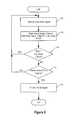
- FIG. 6illustrates operations where the control signal is a gate drive signal for a power field effect transistor (FET) of the SMPS.
- the gate drive signalis continuously monitored at Block 600 .
- An average value of the gate drive signalis determined based on the duty cycle of the gate drive signal at Block 610 .
- the average value of the gate drive signalis compared to a first threshold value Ref 1 and to a second threshold value Ref 2 at Block 620 . More particularly, the average value of the gate drive signal is compared to a range defined between the first and second threshold values Ref 1 and Ref 2 .
- the first threshold value Ref 1may represent an average value of the gate drive signal at a maximum duty cycle
- the second threshold value Ref 2may represent an average value of the gate drive signal at a minimum duty cycle.
- the maximum gate drive duty cyclemay be about 90% or more
- the minimum gate drive duty cyclemay be about 40% or less in some embodiments.
- Block 620if it is determined at Block 620 that the average value of the gate drive signal is within the range defined between the first and second threshold values Ref 1 and Ref 2 , operations return to monitoring the gate drive signal at Block 600 . However, if it is determined at Block 620 that the average value of the gate drive signal falls outside the range defined between the first and second threshold values Ref 1 and Ref 2 , it is determined whether a predetermined time period has expired at Block 630 . For example, a counter may be incremented responsive to determination that the average value is outside the range at Block 620 , and expiration of the predetermined time period may be determined based on the value of the counter.
- a fault signalis provided at Block 640 .
- the predetermined time periodmay be selected based on the period of the gate drive signal and/or the type of fault to be detected. Accordingly, the fault signal is provided when the average value of the gate drive signal, as computed based on its duty cycle, has fallen outside of the range defined by the first and second thresholds Ref 1 and Ref 2 for the predetermined time period.
- the microprocessormay determine that the duty cycle of the gate drive signal needs to be altered based on a feedback signal from the load, and may thereby detect the presence of a fault condition according to the determination, e.g., before actually providing the gate drive signal as an output.
- Embodiments of the present inventionmay be used in any switched mode power application, and are not limited specifically to those described herein.
- fault detection circuitsaccording to some embodiments of the present invention may be used in conjunction with current or voltage pulse width modulated power supplies.
- embodiments of the present inventionmay employ switched-capacitor circuits that have no magnetic storage elements in some embodiments. Such switched-capacitor circuits may be controlled, for example, by the frequency of switching rather than based on the duty cycle of a gate drive signal.
- embodiments of the present inventionmay generally include fault detection based on any characteristics that can be determined from a control signal used to control switching in a switched mode power supply.
- Embodiments of the present inventionmay also be used in linear power supplies and/or other devices that employ a control loop that uses output feedback to generate a control signal.
- Embodiments of the present inventionmay also be used for fault detection in power supplies for driving solid state light sources, such as light emitting diodes (LEDs) used in various applications, including LED lighting systems for general illumination and/or LED backlighting for display technologies.
- LEDslight emitting diodes
- the “PGOOD” signal provided by embodiments of the present inventionmay be used as an indication as to whether the driven LEDs are functioning correctly without the use of a light sensor.
Landscapes
- Physics & Mathematics (AREA)
- General Physics & Mathematics (AREA)
- Dc-Dc Converters (AREA)
Abstract
Description
Claims (28)
Priority Applications (3)
| Application Number | Priority Date | Filing Date | Title |
|---|---|---|---|
| US12/756,573US8680884B2 (en) | 2010-03-25 | 2010-04-08 | Fault detection circuits for switched mode power supplies and related methods of operation |
| EP11759897.9AEP2550714B1 (en) | 2010-03-25 | 2011-03-10 | Fault detection circuits for switched mode power supplies and related methods of operation |
| PCT/US2011/027892WO2011119344A1 (en) | 2010-03-25 | 2011-03-10 | Fault detection circuits for switched mode power supplies and related methods of operation |
Applications Claiming Priority (2)
| Application Number | Priority Date | Filing Date | Title |
|---|---|---|---|
| US31748610P | 2010-03-25 | 2010-03-25 | |
| US12/756,573US8680884B2 (en) | 2010-03-25 | 2010-04-08 | Fault detection circuits for switched mode power supplies and related methods of operation |
Publications (2)
| Publication Number | Publication Date |
|---|---|
| US20110234255A1 US20110234255A1 (en) | 2011-09-29 |
| US8680884B2true US8680884B2 (en) | 2014-03-25 |
Family
ID=44655674
Family Applications (1)
| Application Number | Title | Priority Date | Filing Date |
|---|---|---|---|
| US12/756,573Active2031-12-30US8680884B2 (en) | 2010-03-25 | 2010-04-08 | Fault detection circuits for switched mode power supplies and related methods of operation |
Country Status (3)
| Country | Link |
|---|---|
| US (1) | US8680884B2 (en) |
| EP (1) | EP2550714B1 (en) |
| WO (1) | WO2011119344A1 (en) |
Cited By (15)
| Publication number | Priority date | Publication date | Assignee | Title |
|---|---|---|---|---|
| US20120209936A1 (en)* | 2011-02-15 | 2012-08-16 | Hangzhou Silergy Semiconductor Technology LTD | Communication circuit and method utilizing a single communication line |
| US20130336029A1 (en)* | 2010-12-08 | 2013-12-19 | On-Bright Electronics (Shanghai) Co., Ltd. | System and method providing over current protection based on duty cycle information for power converter |
| US20150091468A1 (en)* | 2013-10-01 | 2015-04-02 | Panasonic Corporation | Lighting device and luminaire using the same |
| US20160209475A1 (en)* | 2013-09-04 | 2016-07-21 | Siemens Aktiengesellschaft | Arrangement and method for monitoring a power supply |
| US9553501B2 (en) | 2010-12-08 | 2017-01-24 | On-Bright Electronics (Shanghai) Co., Ltd. | System and method providing over current protection based on duty cycle information for power converter |
| US9564811B2 (en) | 2014-04-18 | 2017-02-07 | On-Bright Electronics (Shanghai) Co., Ltd. | Systems and methods for regulating output currents of power conversion systems |
| US9577536B2 (en) | 2015-02-02 | 2017-02-21 | On-Bright Electronics (Shanghai) Co., Ltd. | System and method providing reliable over current protection for power converter |
| US9584005B2 (en) | 2014-04-18 | 2017-02-28 | On-Bright Electronics (Shanghai) Co., Ltd. | Systems and methods for regulating output currents of power conversion systems |
| US9614445B2 (en) | 2013-07-19 | 2017-04-04 | On-Bright Electronics (Shanghai) Co., Ltd. | Systems and methods for high precision and/or low loss regulation of output currents of power conversion systems |
| US9647448B2 (en) | 2005-08-18 | 2017-05-09 | On-Bright Electronics (Shanghai) Co., Ltd. | System and method providing over current and over power protection for power converter |
| US9960674B2 (en) | 2015-05-15 | 2018-05-01 | On-Bright Electronics (Shanghai) Co., Ltd. | Systems and methods for output current regulation in power conversion systems |
| US10003268B2 (en) | 2015-05-15 | 2018-06-19 | On-Bright Electronics (Shanghai) Co., Ltd. | Systems and methods for output current regulation in power conversion systems |
| US10483850B1 (en) | 2017-09-18 | 2019-11-19 | Ecosense Lighting Inc. | Universal input-voltage-compatible switched-mode power supply |
| US20210010702A1 (en)* | 2019-07-11 | 2021-01-14 | Johnson Controls Technology Company | Building sensor with self-configuring analog output circuit with fault detection |
| US11016045B2 (en) | 2017-12-18 | 2021-05-25 | Kabushiki Kaisha Toshiba | Inverter device and method for detecting heat dissipation characteristics of inverter device |
Families Citing this family (23)
| Publication number | Priority date | Publication date | Assignee | Title |
|---|---|---|---|---|
| US8077483B2 (en)* | 2007-04-06 | 2011-12-13 | Power Integrations, Inc. | Method and apparatus for sensing multiple voltage values from a single terminal of a power converter controller |
| US8879283B2 (en)* | 2009-11-05 | 2014-11-04 | On-Bright Electronics (Shanghai) Co., Ltd. | System and method providing protection in the event of current sensing failure for power converter |
| US8513941B2 (en)* | 2011-07-30 | 2013-08-20 | Inno-Tech Co., Ltd. | Power detection regulation device |
| GB201116299D0 (en)* | 2011-09-21 | 2011-11-02 | Aker Subsea Ltd | Condition monitoring employing cross-correlation |
| US9093906B2 (en)* | 2011-09-29 | 2015-07-28 | Power Integrations, Inc. | Protection for inadvertent missing feedback voltage signal |
| US9998008B2 (en)* | 2013-01-09 | 2018-06-12 | Infineon Technologies Austria Ag | Active transient response for DC-DC converters |
| JP6095788B2 (en)* | 2013-09-30 | 2017-03-15 | 三菱電機株式会社 | Power converter and air conditioner using the same |
| US9504103B2 (en)* | 2013-10-21 | 2016-11-22 | Osram Sylvania Inc. | Driving a multi-color luminaire |
| CN103997327B (en) | 2014-05-19 | 2017-06-06 | 华为技术有限公司 | A kind of ripple of losing of drive signal detects circuit and switch tube driving circuit |
| US9641070B2 (en) | 2014-06-11 | 2017-05-02 | Allegro Microsystems, Llc | Circuits and techniques for detecting an open pin condition of an integrated circuit |
| US10168721B2 (en)* | 2015-11-02 | 2019-01-01 | Dell Products, L.P. | Controlling redundant power supplies in an information handling system |
| JP6795388B2 (en)* | 2016-12-15 | 2020-12-02 | エイブリック株式会社 | Voltage abnormality detection circuit and semiconductor device |
| FR3062980B1 (en)* | 2017-02-14 | 2021-05-07 | Valeo Comfort & Driving Assistance | LIGHTING SYSTEM, PROCESS IMPLEMENTED IN SUCH A SYSTEM AND ON-BOARD SYSTEM INCLUDING SUCH A SYSTEM |
| US10483794B2 (en)* | 2017-06-28 | 2019-11-19 | Nanning Fugui Precision Industrial Co., Ltd. | Power continuation control circuit |
| US11031804B2 (en)* | 2017-11-06 | 2021-06-08 | Nxp B.V. | Power controller |
| DE102017221657A1 (en) | 2017-12-01 | 2019-06-06 | Continental Automotive Gmbh | Method for carrying out a self-test of an electrical converter circuit and converter circuit and vehicle light |
| CN108303636B (en)* | 2018-01-25 | 2023-06-13 | 昆明理工大学 | Device and method for detecting quality of Buck-Boost integrated voltage stabilizing chip |
| DE102018122649A1 (en)* | 2018-09-17 | 2020-03-19 | Infineon Technologies Ag | Electronic circuit with a led module |
| US11079443B2 (en)* | 2018-12-21 | 2021-08-03 | Analog Devices International Unlimited Company | Switch fault detection techniques for DC-DC converters |
| FR3114657B1 (en)* | 2020-09-30 | 2022-10-07 | Schneider Electric Ind Sas | Methods and systems for identifying a failed current sensor |
| US11811320B2 (en)* | 2021-12-16 | 2023-11-07 | Richtek Technology Corporation | Power conversion circuit having short-circuit detection function and short-circuit detection method thereof |
| FR3146522A1 (en)* | 2023-03-08 | 2024-09-13 | Stmicroelectronics International N.V. | Short circuit detection circuit |
| CN116560145A (en)* | 2023-05-30 | 2023-08-08 | 中国银行股份有限公司 | A detection device, detection method, electronic equipment and storage medium |
Citations (23)
| Publication number | Priority date | Publication date | Assignee | Title |
|---|---|---|---|---|
| US4270164A (en)* | 1979-02-28 | 1981-05-26 | Contraves Goerz Corporation | Short circuit protection for switching type power processors |
| US5122726A (en)* | 1990-10-31 | 1992-06-16 | Alcatel Network Systems, Inc. | Overvoltage protection for redundant power supplies |
| US5315256A (en)* | 1991-05-20 | 1994-05-24 | Cox & Company, Inc. | Fault detection circuit for use in determining the existence of a fault in any one of a plurality of DC loads |
| US5525913A (en)* | 1994-10-19 | 1996-06-11 | Intel Corporation | Power validation tool for microprocessor systems |
| US5754036A (en) | 1996-07-25 | 1998-05-19 | Lti International, Inc. | Energy saving power control system and method |
| US5861735A (en)* | 1997-02-27 | 1999-01-19 | Nec Corporation | Switching power supply circuit |
| US5995001A (en)* | 1997-07-09 | 1999-11-30 | Crown Equipment Corporation | Method and apparatus for providing operating information to an operator of a fork lift truck |
| US6092992A (en) | 1996-10-24 | 2000-07-25 | Imblum; Gregory G. | System and method for pump control and fault detection |
| US6191569B1 (en) | 1999-12-03 | 2001-02-20 | Lucent Technologies Inc. | Circuit and method for generating estimated feedback for the controller of a slave power module in a master/slave paralleling scheme |
| US20010009517A1 (en)* | 2000-01-20 | 2001-07-26 | Peter Preller | Method for switching off a switched-mode power supply in the event of short-circuit, and a switched- mode power supply |
| US20040189348A1 (en)* | 2003-03-28 | 2004-09-30 | Tallant James C. | Asynchronous fault detection circuit for a PWM driver |
| US6853174B1 (en)* | 2003-08-11 | 2005-02-08 | Micrel, Inc. | Selective high-side and low-side current sensing in switching power supplies |
| US20050285619A1 (en)* | 2004-06-25 | 2005-12-29 | General Electric Company | System and method for detecting an operational fault condition in a power supply |
| US20060279970A1 (en) | 2002-11-14 | 2006-12-14 | Kent Kernahan | Switching power converter controller |
| US20070153439A1 (en)* | 2006-01-03 | 2007-07-05 | Semiconductor Components Industries, Llc. | Fault control circuit and method therefor |
| US20070200610A1 (en) | 2004-08-06 | 2007-08-30 | Stmicroelectronics S.A. | Switched-mode power supply regulation |
| US20080046204A1 (en) | 2006-08-16 | 2008-02-21 | Aaron Jungreis | Power outage detection in a switched mode power supply |
| US7449912B2 (en)* | 2007-01-26 | 2008-11-11 | Hewlett-Packard Development Company, L.P. | Fault detection circuit |
| US7595615B2 (en) | 2005-04-05 | 2009-09-29 | Texas Instruments Incorporated | Systems and methods for providing over-current protection in a switching power supply |
| US20100085024A1 (en)* | 2008-10-02 | 2010-04-08 | Intersil Americas Inc. | Power supply controller with different steady state and transient response characteristics |
| US20100110738A1 (en)* | 2008-11-04 | 2010-05-06 | Fuji Electric Systems Co., Ltd. | Switching power supply apparatus |
| US7881027B2 (en)* | 1998-11-16 | 2011-02-01 | Power Integrations, Inc. | Fault condition protection |
| US8093878B2 (en)* | 2008-07-28 | 2012-01-10 | Texas Instruments Incorporated | Switching power supply device |
Family Cites Families (6)
| Publication number | Priority date | Publication date | Assignee | Title |
|---|---|---|---|---|
| US5307256A (en) | 1992-12-17 | 1994-04-26 | Silverstein Robert A | Trickle charge circuit for an off-line switching power supply |
| DE19853626A1 (en)* | 1998-11-20 | 2000-05-31 | Texas Instruments Deutschland | Switching regulator has upward and downward modes enabled with periodic control by switch control circuit; pulse duration modulator varies duty cycle correct output voltage errors |
| US6385060B1 (en)* | 2000-12-21 | 2002-05-07 | Semiconductor Components Industries Llc | Switching power supply with reduced energy transfer during a fault condition |
| US6552578B1 (en)* | 2002-06-10 | 2003-04-22 | Pericom Semiconductor Corp. | Power down circuit detecting duty cycle of input signal |
| JP4262753B2 (en)* | 2007-01-04 | 2009-05-13 | 日本航空電子工業株式会社 | Short-circuit detection circuit, RD converter, and digital angle detection device |
| US8598855B2 (en)* | 2008-03-12 | 2013-12-03 | O2Micro, Inc. | Monitoring and control circuit for adjusting current |
- 2010
- 2010-04-08USUS12/756,573patent/US8680884B2/enactiveActive
- 2011
- 2011-03-10WOPCT/US2011/027892patent/WO2011119344A1/enactiveApplication Filing
- 2011-03-10EPEP11759897.9Apatent/EP2550714B1/enactiveActive
Patent Citations (24)
| Publication number | Priority date | Publication date | Assignee | Title |
|---|---|---|---|---|
| US4270164A (en)* | 1979-02-28 | 1981-05-26 | Contraves Goerz Corporation | Short circuit protection for switching type power processors |
| US5122726A (en)* | 1990-10-31 | 1992-06-16 | Alcatel Network Systems, Inc. | Overvoltage protection for redundant power supplies |
| US5315256A (en)* | 1991-05-20 | 1994-05-24 | Cox & Company, Inc. | Fault detection circuit for use in determining the existence of a fault in any one of a plurality of DC loads |
| US5525913A (en)* | 1994-10-19 | 1996-06-11 | Intel Corporation | Power validation tool for microprocessor systems |
| US5754036A (en) | 1996-07-25 | 1998-05-19 | Lti International, Inc. | Energy saving power control system and method |
| US6092992A (en) | 1996-10-24 | 2000-07-25 | Imblum; Gregory G. | System and method for pump control and fault detection |
| US5861735A (en)* | 1997-02-27 | 1999-01-19 | Nec Corporation | Switching power supply circuit |
| US5995001A (en)* | 1997-07-09 | 1999-11-30 | Crown Equipment Corporation | Method and apparatus for providing operating information to an operator of a fork lift truck |
| US7881027B2 (en)* | 1998-11-16 | 2011-02-01 | Power Integrations, Inc. | Fault condition protection |
| US20120206842A1 (en)* | 1998-11-16 | 2012-08-16 | Power Integrations, Inc. | Fault condition protection |
| US6191569B1 (en) | 1999-12-03 | 2001-02-20 | Lucent Technologies Inc. | Circuit and method for generating estimated feedback for the controller of a slave power module in a master/slave paralleling scheme |
| US20010009517A1 (en)* | 2000-01-20 | 2001-07-26 | Peter Preller | Method for switching off a switched-mode power supply in the event of short-circuit, and a switched- mode power supply |
| US20060279970A1 (en) | 2002-11-14 | 2006-12-14 | Kent Kernahan | Switching power converter controller |
| US20040189348A1 (en)* | 2003-03-28 | 2004-09-30 | Tallant James C. | Asynchronous fault detection circuit for a PWM driver |
| US6853174B1 (en)* | 2003-08-11 | 2005-02-08 | Micrel, Inc. | Selective high-side and low-side current sensing in switching power supplies |
| US20050285619A1 (en)* | 2004-06-25 | 2005-12-29 | General Electric Company | System and method for detecting an operational fault condition in a power supply |
| US20070200610A1 (en) | 2004-08-06 | 2007-08-30 | Stmicroelectronics S.A. | Switched-mode power supply regulation |
| US7595615B2 (en) | 2005-04-05 | 2009-09-29 | Texas Instruments Incorporated | Systems and methods for providing over-current protection in a switching power supply |
| US20070153439A1 (en)* | 2006-01-03 | 2007-07-05 | Semiconductor Components Industries, Llc. | Fault control circuit and method therefor |
| US20080046204A1 (en) | 2006-08-16 | 2008-02-21 | Aaron Jungreis | Power outage detection in a switched mode power supply |
| US7449912B2 (en)* | 2007-01-26 | 2008-11-11 | Hewlett-Packard Development Company, L.P. | Fault detection circuit |
| US8093878B2 (en)* | 2008-07-28 | 2012-01-10 | Texas Instruments Incorporated | Switching power supply device |
| US20100085024A1 (en)* | 2008-10-02 | 2010-04-08 | Intersil Americas Inc. | Power supply controller with different steady state and transient response characteristics |
| US20100110738A1 (en)* | 2008-11-04 | 2010-05-06 | Fuji Electric Systems Co., Ltd. | Switching power supply apparatus |
Non-Patent Citations (2)
| Title |
|---|
| International Preliminary Report on Patentability Corresponding to International Application No. PCT/US2011/027892; Date of Mailing: Oct. 4, 2012; 8 Pages. |
| International Search Report and the Written Opinion of the International Searching Authority corresponding to International Application No. PCT/US2011/027892; Date of Mailing: May 4, 2011; 10 Pages. |
Cited By (43)
| Publication number | Priority date | Publication date | Assignee | Title |
|---|---|---|---|---|
| US9647448B2 (en) | 2005-08-18 | 2017-05-09 | On-Bright Electronics (Shanghai) Co., Ltd. | System and method providing over current and over power protection for power converter |
| US9548652B2 (en)* | 2010-12-08 | 2017-01-17 | On-Bright Electronics (Shanghai) Co., Ltd. | System and method providing over current protection based on duty cycle information for power converter |
| US11264888B2 (en) | 2010-12-08 | 2022-03-01 | On-Bright Electronics (Shanghai) Co., Ltd. | System and method providing over current protection based on duty cycle information for power converter |
| US11114933B2 (en) | 2010-12-08 | 2021-09-07 | On-Bright Electronics (Shanghai) Co., Ltd. | System and method providing over current protection based on duty cycle information for power converter |
| US10811955B2 (en) | 2010-12-08 | 2020-10-20 | On-Bright Electronics (Shanghai) Co., Ltd. | System and method providing over current protection based on duty cycle information for power converter |
| US20130336029A1 (en)* | 2010-12-08 | 2013-12-19 | On-Bright Electronics (Shanghai) Co., Ltd. | System and method providing over current protection based on duty cycle information for power converter |
| US9553501B2 (en) | 2010-12-08 | 2017-01-24 | On-Bright Electronics (Shanghai) Co., Ltd. | System and method providing over current protection based on duty cycle information for power converter |
| US10615684B2 (en) | 2010-12-08 | 2020-04-07 | On-Bright Electronics (Shanghai) Co., Ltd. | System and method providing over current protection based on duty cycle information for power converter |
| US10581315B2 (en) | 2010-12-08 | 2020-03-03 | On-Bright Electronics (Shanghai) Co., Ltd. | System and method providing over current protection based on duty cycle information for power converter |
| US10483838B2 (en) | 2010-12-08 | 2019-11-19 | On-Bright Electronics (Shanghai) Co., Ltd. | System and method providing over current protection based on duty cycle information for power converter |
| US10277110B2 (en) | 2010-12-08 | 2019-04-30 | On-Bright Electronics (Shanghai) Co., Ltd. | System and method providing over current protection based on duty cycle information for power converter |
| US8788610B2 (en)* | 2011-02-15 | 2014-07-22 | Silergy Semiconductor Technology (Hangzhou) Ltd. | Communication circuit and method utilizing a single communication line |
| US20120209936A1 (en)* | 2011-02-15 | 2012-08-16 | Hangzhou Silergy Semiconductor Technology LTD | Communication circuit and method utilizing a single communication line |
| US10177665B2 (en) | 2013-07-19 | 2019-01-08 | On-Bright Electronics (Shanghai) Co., Ltd. | Systems and methods for high precision and/or low loss regulation of output currents of power conversion systems |
| US9614445B2 (en) | 2013-07-19 | 2017-04-04 | On-Bright Electronics (Shanghai) Co., Ltd. | Systems and methods for high precision and/or low loss regulation of output currents of power conversion systems |
| US11108328B2 (en) | 2013-07-19 | 2021-08-31 | On-Bright Electronics (Shanghai) Co., Ltd. | Systems and methods for high precision and/or low loss regulation of output currents of power conversion systems |
| US10211740B2 (en) | 2013-07-19 | 2019-02-19 | On-Bright Electronics (Shanghai) Co., Ltd. | Systems and methods for high precision and/or low loss regulation of output currents of power conversion systems |
| US20160209475A1 (en)* | 2013-09-04 | 2016-07-21 | Siemens Aktiengesellschaft | Arrangement and method for monitoring a power supply |
| US9869727B2 (en)* | 2013-09-04 | 2018-01-16 | Siemens Aktiengesellschaft | Arrangement and method for monitoring a power supply |
| US9320106B2 (en)* | 2013-10-01 | 2016-04-19 | Panasonic Intellectual Property Management Co., Ltd. | Lighting device and luminaire using the same |
| US20150091468A1 (en)* | 2013-10-01 | 2015-04-02 | Panasonic Corporation | Lighting device and luminaire using the same |
| US10044254B2 (en) | 2014-04-18 | 2018-08-07 | On-Bright Electronics (Shanghai) Co., Ltd. | Systems and methods for regulating output currents of power conversion systems |
| US10170999B2 (en) | 2014-04-18 | 2019-01-01 | On-Bright Electronics (Shanghai) Co., Ltd. | Systems and methods for regulating output currents of power conversion systems |
| US9991802B2 (en) | 2014-04-18 | 2018-06-05 | On-Bright Electronics (Shanghai) Co., Ltd. | Systems and methods for regulating output currents of power conversion systems |
| US9584005B2 (en) | 2014-04-18 | 2017-02-28 | On-Bright Electronics (Shanghai) Co., Ltd. | Systems and methods for regulating output currents of power conversion systems |
| US9564811B2 (en) | 2014-04-18 | 2017-02-07 | On-Bright Electronics (Shanghai) Co., Ltd. | Systems and methods for regulating output currents of power conversion systems |
| US10686359B2 (en) | 2014-04-18 | 2020-06-16 | On-Bright Electronics (Shanghai) Co., Ltd. | Systems and methods for regulating output currents of power conversion systems |
| US9570986B2 (en) | 2014-04-18 | 2017-02-14 | On-Bright Electronics (Shanghai) Co., Ltd. | Systems and methods for regulating output currents of power conversion systems |
| US10211626B2 (en) | 2015-02-02 | 2019-02-19 | On-Bright Electronics (Shanghai) Co., Ltd. | System and method providing reliable over current protection for power converter |
| US9577536B2 (en) | 2015-02-02 | 2017-02-21 | On-Bright Electronics (Shanghai) Co., Ltd. | System and method providing reliable over current protection for power converter |
| US10811965B2 (en) | 2015-05-15 | 2020-10-20 | On-Bright Electronics (Shanghai) Co., Ltd. | Systems and methods for output current regulation in power conversion systems |
| US10680525B2 (en) | 2015-05-15 | 2020-06-09 | On-Bright Electronics (Shanghai) Co., Ltd. | Systems and methods for output current regulation in power conversion systems |
| US10686373B2 (en) | 2015-05-15 | 2020-06-16 | On-Bright Electronics (Shanghai) Co., Ltd. | Systems and methods for output current regulation in power conversion systems |
| US10432096B2 (en) | 2015-05-15 | 2019-10-01 | On-Bright Electronics (Shanghai) Co., Ltd. | Systems and methods for output current regulation in power conversion systems |
| US10340795B2 (en) | 2015-05-15 | 2019-07-02 | On-Bright Electronics (Shanghai) Co., Ltd. | Systems and methods for output current regulation in power conversion systems |
| US10270334B2 (en) | 2015-05-15 | 2019-04-23 | On-Bright Electronics (Shanghai) Co., Ltd. | Systems and methods for output current regulation in power conversion systems |
| US10003268B2 (en) | 2015-05-15 | 2018-06-19 | On-Bright Electronics (Shanghai) Co., Ltd. | Systems and methods for output current regulation in power conversion systems |
| US9960674B2 (en) | 2015-05-15 | 2018-05-01 | On-Bright Electronics (Shanghai) Co., Ltd. | Systems and methods for output current regulation in power conversion systems |
| US11652410B2 (en) | 2015-05-15 | 2023-05-16 | On-Bright Electronics (Shanghai) Co., Ltd. | Systems and methods for output current regulation in power conversion systems |
| US10483850B1 (en) | 2017-09-18 | 2019-11-19 | Ecosense Lighting Inc. | Universal input-voltage-compatible switched-mode power supply |
| US11016045B2 (en) | 2017-12-18 | 2021-05-25 | Kabushiki Kaisha Toshiba | Inverter device and method for detecting heat dissipation characteristics of inverter device |
| US20210010702A1 (en)* | 2019-07-11 | 2021-01-14 | Johnson Controls Technology Company | Building sensor with self-configuring analog output circuit with fault detection |
| US12104808B2 (en)* | 2019-07-11 | 2024-10-01 | Tyco Fire & Security Gmbh | Building sensor with self-configuring analog output circuit with fault detection |
Also Published As
| Publication number | Publication date |
|---|---|
| EP2550714A1 (en) | 2013-01-30 |
| EP2550714A4 (en) | 2017-03-29 |
| EP2550714B1 (en) | 2023-03-08 |
| WO2011119344A1 (en) | 2011-09-29 |
| US20110234255A1 (en) | 2011-09-29 |
Similar Documents
| Publication | Publication Date | Title |
|---|---|---|
| US8680884B2 (en) | Fault detection circuits for switched mode power supplies and related methods of operation | |
| US8680778B2 (en) | LED driver circuit | |
| US9473032B2 (en) | Power converter system with synchronous rectifier output stage and reduced no-load power consumption | |
| US9621068B2 (en) | Load driving circuit and method thereof | |
| US7550934B1 (en) | LED driver with fast open circuit protection, short circuit compensation, and rapid brightness control response | |
| EP2364061B1 (en) | Circuits and methods for driving light sources | |
| US8143800B2 (en) | Circuits and methods for driving a load with power factor correction function | |
| EP1884141B1 (en) | Two-wire dimmer with power supply and load protection circuit in the event of switch failure | |
| JP6104511B2 (en) | Controller, system, and method for controlling dimming of a light source | |
| JP5960611B2 (en) | Reduced power loss power system, electronic device and controller | |
| CN103368143B (en) | Current mode switch power supply overpower-protection circuit | |
| US20120074782A1 (en) | System and method for load control | |
| CN102299630A (en) | Power converter with compensation circuit for adjusting output current provided to a constant load | |
| US8754625B2 (en) | System and method for converting an AC input voltage to regulated output current | |
| EP2751894A1 (en) | Wall box device for managing energy | |
| GB2476609A (en) | Operating circuit for LEDs | |
| CN104247564A (en) | Operation method of LLC resonant converter for lighting device, converter and LED converter | |
| US10021754B2 (en) | Two-channel LED driver with short circuit protection and short circuit protection method for two-channel LED driver | |
| US9125258B2 (en) | Light source driving apparatus, light source device including the same and light source driving method of the light source driving apparatus | |
| EP3192327B1 (en) | Led dimmer circuit and method | |
| US20130264879A1 (en) | Low power consumption backup power system | |
| KR102645224B1 (en) | Power supply supporting device and controlling method thereof | |
| TW201351864A (en) | Independently adjustable current and voltage AC to AC converter | |
| US10804813B2 (en) | Power inverter for reducing total harmonic distortion via duty cycle control | |
| US20100052556A1 (en) | Digital Control Circuit of an Operating Device for Lamps |
Legal Events
| Date | Code | Title | Description |
|---|---|---|---|
| AS | Assignment | Owner name:CREE LED LIGHTING SOLUTIONS, INC., NORTH CAROLINA Free format text:ASSIGNMENT OF ASSIGNORS INTEREST;ASSIGNOR:CHOBOT, JOSEPH PAUL;REEL/FRAME:024207/0469 Effective date:20100408 | |
| AS | Assignment | Owner name:CREE, INC., NORTH CAROLINA Free format text:MERGER;ASSIGNOR:CREE LED LIGHTING SOLUTIONS, INC.;REEL/FRAME:024673/0786 Effective date:20100621 | |
| STCF | Information on status: patent grant | Free format text:PATENTED CASE | |
| MAFP | Maintenance fee payment | Free format text:PAYMENT OF MAINTENANCE FEE, 4TH YEAR, LARGE ENTITY (ORIGINAL EVENT CODE: M1551) Year of fee payment:4 | |
| AS | Assignment | Owner name:IDEAL INDUSTRIES LIGHTING LLC, ILLINOIS Free format text:ASSIGNMENT OF ASSIGNORS INTEREST;ASSIGNOR:CREE, INC.;REEL/FRAME:049223/0494 Effective date:20190513 | |
| MAFP | Maintenance fee payment | Free format text:PAYMENT OF MAINTENANCE FEE, 8TH YEAR, LARGE ENTITY (ORIGINAL EVENT CODE: M1552); ENTITY STATUS OF PATENT OWNER: LARGE ENTITY Year of fee payment:8 | |
| AS | Assignment | Owner name:FGI WORLDWIDE LLC, NEW YORK Free format text:SECURITY INTEREST;ASSIGNOR:IDEAL INDUSTRIES LIGHTING LLC;REEL/FRAME:064897/0413 Effective date:20230908 |