US8680589B2 - Omega shaped nanowire field effect transistors - Google Patents
Omega shaped nanowire field effect transistorsDownload PDFInfo
- Publication number
- US8680589B2 US8680589B2US13/372,719US201213372719AUS8680589B2US 8680589 B2US8680589 B2US 8680589B2US 201213372719 AUS201213372719 AUS 201213372719AUS 8680589 B2US8680589 B2US 8680589B2
- Authority
- US
- United States
- Prior art keywords
- silicon
- nanowire
- doped
- distal end
- epi
- Prior art date
- Legal status (The legal status is an assumption and is not a legal conclusion. Google has not performed a legal analysis and makes no representation as to the accuracy of the status listed.)
- Active
Links
Images


Classifications
- H—ELECTRICITY
- H10—SEMICONDUCTOR DEVICES; ELECTRIC SOLID-STATE DEVICES NOT OTHERWISE PROVIDED FOR
- H10D—INORGANIC ELECTRIC SEMICONDUCTOR DEVICES
- H10D30/00—Field-effect transistors [FET]
- H10D30/40—FETs having zero-dimensional [0D], one-dimensional [1D] or two-dimensional [2D] charge carrier gas channels
- H10D30/43—FETs having zero-dimensional [0D], one-dimensional [1D] or two-dimensional [2D] charge carrier gas channels having 1D charge carrier gas channels, e.g. quantum wire FETs or transistors having 1D quantum-confined channels
- B—PERFORMING OPERATIONS; TRANSPORTING
- B82—NANOTECHNOLOGY
- B82Y—SPECIFIC USES OR APPLICATIONS OF NANOSTRUCTURES; MEASUREMENT OR ANALYSIS OF NANOSTRUCTURES; MANUFACTURE OR TREATMENT OF NANOSTRUCTURES
- B82Y10/00—Nanotechnology for information processing, storage or transmission, e.g. quantum computing or single electron logic
- H—ELECTRICITY
- H10—SEMICONDUCTOR DEVICES; ELECTRIC SOLID-STATE DEVICES NOT OTHERWISE PROVIDED FOR
- H10D—INORGANIC ELECTRIC SEMICONDUCTOR DEVICES
- H10D30/00—Field-effect transistors [FET]
- H10D30/01—Manufacture or treatment
- H10D30/014—Manufacture or treatment of FETs having zero-dimensional [0D] or one-dimensional [1D] channels, e.g. quantum wire FETs, single-electron transistors [SET] or Coulomb blockade transistors
- H—ELECTRICITY
- H10—SEMICONDUCTOR DEVICES; ELECTRIC SOLID-STATE DEVICES NOT OTHERWISE PROVIDED FOR
- H10D—INORGANIC ELECTRIC SEMICONDUCTOR DEVICES
- H10D30/00—Field-effect transistors [FET]
- H10D30/01—Manufacture or treatment
- H10D30/021—Manufacture or treatment of FETs having insulated gates [IGFET]
- H10D30/027—Manufacture or treatment of FETs having insulated gates [IGFET] of lateral single-gate IGFETs
- H10D30/0275—Manufacture or treatment of FETs having insulated gates [IGFET] of lateral single-gate IGFETs forming single crystalline semiconductor source or drain regions resulting in recessed gates, e.g. forming raised source or drain regions
- H—ELECTRICITY
- H10—SEMICONDUCTOR DEVICES; ELECTRIC SOLID-STATE DEVICES NOT OTHERWISE PROVIDED FOR
- H10D—INORGANIC ELECTRIC SEMICONDUCTOR DEVICES
- H10D30/00—Field-effect transistors [FET]
- H10D30/01—Manufacture or treatment
- H10D30/021—Manufacture or treatment of FETs having insulated gates [IGFET]
- H10D30/031—Manufacture or treatment of FETs having insulated gates [IGFET] of thin-film transistors [TFT]
- H10D30/0321—Manufacture or treatment of FETs having insulated gates [IGFET] of thin-film transistors [TFT] comprising silicon, e.g. amorphous silicon or polysilicon
- H10D30/0323—Manufacture or treatment of FETs having insulated gates [IGFET] of thin-film transistors [TFT] comprising silicon, e.g. amorphous silicon or polysilicon comprising monocrystalline silicon
- H—ELECTRICITY
- H10—SEMICONDUCTOR DEVICES; ELECTRIC SOLID-STATE DEVICES NOT OTHERWISE PROVIDED FOR
- H10D—INORGANIC ELECTRIC SEMICONDUCTOR DEVICES
- H10D30/00—Field-effect transistors [FET]
- H10D30/60—Insulated-gate field-effect transistors [IGFET]
- H10D30/67—Thin-film transistors [TFT]
- H10D30/6729—Thin-film transistors [TFT] characterised by the electrodes
- H10D30/673—Thin-film transistors [TFT] characterised by the electrodes characterised by the shapes, relative sizes or dispositions of the gate electrodes
- H10D30/6733—Multi-gate TFTs
- H—ELECTRICITY
- H10—SEMICONDUCTOR DEVICES; ELECTRIC SOLID-STATE DEVICES NOT OTHERWISE PROVIDED FOR
- H10D—INORGANIC ELECTRIC SEMICONDUCTOR DEVICES
- H10D30/00—Field-effect transistors [FET]
- H10D30/60—Insulated-gate field-effect transistors [IGFET]
- H10D30/67—Thin-film transistors [TFT]
- H10D30/6729—Thin-film transistors [TFT] characterised by the electrodes
- H10D30/673—Thin-film transistors [TFT] characterised by the electrodes characterised by the shapes, relative sizes or dispositions of the gate electrodes
- H10D30/6735—Thin-film transistors [TFT] characterised by the electrodes characterised by the shapes, relative sizes or dispositions of the gate electrodes having gates fully surrounding the channels, e.g. gate-all-around
- H—ELECTRICITY
- H10—SEMICONDUCTOR DEVICES; ELECTRIC SOLID-STATE DEVICES NOT OTHERWISE PROVIDED FOR
- H10D—INORGANIC ELECTRIC SEMICONDUCTOR DEVICES
- H10D30/00—Field-effect transistors [FET]
- H10D30/60—Insulated-gate field-effect transistors [IGFET]
- H10D30/67—Thin-film transistors [TFT]
- H10D30/6757—Thin-film transistors [TFT] characterised by the structure of the channel, e.g. transverse or longitudinal shape or doping profile
- H—ELECTRICITY
- H10—SEMICONDUCTOR DEVICES; ELECTRIC SOLID-STATE DEVICES NOT OTHERWISE PROVIDED FOR
- H10D—INORGANIC ELECTRIC SEMICONDUCTOR DEVICES
- H10D62/00—Semiconductor bodies, or regions thereof, of devices having potential barriers
- H10D62/10—Shapes, relative sizes or dispositions of the regions of the semiconductor bodies; Shapes of the semiconductor bodies
- H10D62/117—Shapes of semiconductor bodies
- H10D62/118—Nanostructure semiconductor bodies
- H—ELECTRICITY
- H10—SEMICONDUCTOR DEVICES; ELECTRIC SOLID-STATE DEVICES NOT OTHERWISE PROVIDED FOR
- H10D—INORGANIC ELECTRIC SEMICONDUCTOR DEVICES
- H10D86/00—Integrated devices formed in or on insulating or conducting substrates, e.g. formed in silicon-on-insulator [SOI] substrates or on stainless steel or glass substrates
- H10D86/01—Manufacture or treatment
- H10D86/011—Manufacture or treatment comprising FinFETs
- H—ELECTRICITY
- H10—SEMICONDUCTOR DEVICES; ELECTRIC SOLID-STATE DEVICES NOT OTHERWISE PROVIDED FOR
- H10D—INORGANIC ELECTRIC SEMICONDUCTOR DEVICES
- H10D86/00—Integrated devices formed in or on insulating or conducting substrates, e.g. formed in silicon-on-insulator [SOI] substrates or on stainless steel or glass substrates
- H10D86/201—Integrated devices formed in or on insulating or conducting substrates, e.g. formed in silicon-on-insulator [SOI] substrates or on stainless steel or glass substrates the substrates comprising an insulating layer on a semiconductor body, e.g. SOI
- H10D86/215—Integrated devices formed in or on insulating or conducting substrates, e.g. formed in silicon-on-insulator [SOI] substrates or on stainless steel or glass substrates the substrates comprising an insulating layer on a semiconductor body, e.g. SOI comprising FinFETs
Definitions
- the present inventionrelates to semiconductor nanowire field effect transistors.
- a nanowire field effect transistorincludes doped portions of nanowire that contact the channel region and serve as source and drain regions of the device. Previous fabrication methods that used ion-implantation to dope the small diameter nanowire may result in undesirable amorphization of the nanowire or an undesirable junction doping profile.
- a method for forming a nanowire field effect transistor (FET) deviceincludes forming a nanowire on a semiconductor substrate, forming a first gate structure on a first portion of the nanowire, forming a first protective spacer adjacent to sidewalls of the first gate structure and over portions of the nanowire extending from the first gate structure, removing exposed portions of the nanowire left unprotected by the first spacer, and epitaxially growing a doped semiconductor material on exposed cross sections of the nanowire to form a first source region and a first drain region
- a method for a nanowire field effect transistor (FET) deviceincludes forming a nanowire on a semiconductor substrate, forming a gate structure on a portion of the nanowire, forming a protective spacer adjacent to sidewalls of the gate structure and over portions of the nanowire extending from the gate structure, removing exposed portions of the nanowire to form a cavity defined by the nanowire surrounded by the gate structure, the semiconductor substrate, and the spacer, and epitaxially growing a doped semiconductor material in the cavity from exposed cross sections of the nanowire.
- FETnanowire field effect transistor
- a nanowire field effect transistor (FET) devicein yet another aspect of the present invention, includes a channel region including a silicon portion disposed on a semiconductor substrate having a first distal end extending from the channel region and a second distal end extending from the channel region, the silicon portion is partially surrounded by a gate structure disposed circumferentially on the silicon portion, a source region including a first doped epi-silicon nanowire extension contacting the first distal end of the silicon portion, and a drain region including a second doped epi-silicon nanowire extension contacting the second distal end of the silicon portion.
- FETnanowire field effect transistor
- a nanowire field effect transistor (FET) devicein yet another aspect of the present invention, includes a channel region disposed on a semiconductor substrate including a silicon portion having a first distal end and a second distal end, the silicon portion is surrounded by a gate structure disposed circumferentially on the silicon portion, a first cavity defined by the first distal end of the silicon portion, the semiconductor substrate, and an inner diameter of the gate structure, a second cavity defined by the second distal end of the silicon portion, the semiconductor substrate, and an inner diameter of the gate structure, a source region including a first doped epi-silicon nanowire extension epitaxially extending from the first distal end of the silicon portion in the first cavity, and a drain region including a second doped epi-silicon nanowire extension epitaxially extending from the second distal end of the silicon portion in the second cavity.
- FETnanowire field effect transistor
- FIGS. 1-12Billustrate an exemplary method for forming field effect transistor (FET) devices.
- FIGS. 13A-14Billustrate an alternate exemplary method for forming field effect transistor (FET) devices.
- a silicon on insulator (SOI) portion 102is defined on a buried oxide (BOX) layer 104 that is disposed on a silicon substrate 100 .
- the SOI portion 102includes a SOI pad region 106 , a SOI pad region 108 , and nanowire portions 109 .
- the SOI portion 102may be patterned by the use of lithography followed by an etching process such as, for example, reactive ion etching (RIE).
- RIEreactive ion etching
- FIG. 2illustrates the nanowires 110 disposed on the BOX layer 104 following an oxidation process that reduces the diameter of the nanowires 110 .
- the reduction of the diameter of the nanowires 110may be performed by, for example, an oxidation of the nanowires 110 followed by the etching of the grown oxide. The oxidation and etching process may be repeated to achieve a desired nanowire 110 diameter.
- gatesare formed over the channel regions of the nanowires 110 (described below).
- FIG. 3Aillustrates gates 402 that are formed on the nanowires 110 , as described in further detail below, and capped with a polysilicon layer (capping layer) 404 .
- a hardmask layer 406such as, for example silicon nitride (Si 3 N 4 ) is deposited over the polysilicon layer 404 .
- the polysilicon layer 404 and the hardmask layer 406may be formed by depositing polysilicon material over the BOX layer 104 and the SOI portion 102 , depositing the hardmask material over the polysilicon material, and etching by RIE to form the polysilicon layer 406 and the hardmask layer 404 illustrated in FIG. 3A .
- the etching of the gate 402may be performed by directional etching that results in straight sidewalls of the gate 402 .
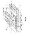
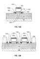
- FIG. 3Billustrates a perspective view of an exemplary alternate arrangement that includes a plurality of gates 402 that are formed on the nanowires 110 between SOI pad regions 106 and 108 .
- the fabrication of the arrangement shown in FIG. 3Bmay be performed using similar methods as described above for the fabrication of a single row of gates 402 line, and illustrates how the methods described herein may be used to form any number of devices on a nanowire between SOI pad regions 106 and 108 .
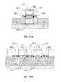
- FIG. 4illustrates a cross sectional view of a gate 402 along the line A-A (of FIG. 3A ).
- the gate 402is formed by depositing a first gate dielectric layer 502 , such as silicon dioxide (SiO 2 ) on a channel portion of the nanowire 110 .
- a second gate dielectric layer 504such as, for example, hafnium oxide (HfO 2 ) is formed on the first gate dielectric layer 502 .
- a metal layer 506such as, for example, tantalum nitride (TaN) is formed on the second gate dielectric layer 504 .
- the metal layer 506is surrounded by polysilicon layer 404 (of FIG. 3A ). Doping the polysilicon layer 404 with impurities such as boron (p-type), or phosphorus (n-type) makes the polysilicon layer 404 conductive.
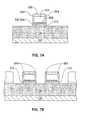
- FIGS. 5A and 5Billustrate the spacer portions 604 formed along opposing sides of the polysilicon layer 404 .
- the spacersare formed by depositing a blanket dielectric film such as silicon nitride and etching the dielectric film from all horizontal surfaces by RIE.
- the spacer walls 604are formed around portions of the nanowire 110 that extend from the polysilicon layer 404 and surround portions of the nanowires 110 .
- FIGS. 5A and 5Binclude spacer portions 602 that are formed under the nanowires 110 , and in the undercut regions 202 (of FIG. 2 ).
- FIG. 6Aillustrates a cross-sectional view (of FIG. 5A ).
- FIG. 6Billustrates a similar cross-sectional view of the exemplary alternate arrangement of FIG. 5B .
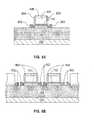
- FIGS. 7A and 7Billustrate cross-sectional views of the resultant structures following a selective RIE process, that removes exposed portions of the nanowires 110 and the SOI pad regions 106 and 108 (shown in FIG. 6A ).
- An example of a selective RIE processincludes a RIE based on HBr chemistry that etches silicon while being selective to reduce the etching of dielectrics such as silicon oxide and silicon nitride.
- the portions of the nanowire 110 that are surrounded by the spacer walls 604are not etched, and have exposed cross sections defined by the spacer walls 604 .
- FIGS. 8A and 8Billustrate cross-sectional views of the resultant structures following a selective epi-silicon growth to form epi-nanowire extensions 902 (nanowire extensions).
- the nanowire extensions 902are epitaxially grown from the exposed cross-sectional portions of the nanowire 110 that are surrounded by the spacer walls 604 .
- the nanowire extensions 902are formed by epitaxially growing, for example, in-situ doped silicon (Si) or a silicon germanium (SiGe) that may be either n-type or p-type doped.
- the in-situ doped epi processforms the source region and the drain region of the nanowire FET.
- a chemical vapor deposition (CVD) reactormay be used to perform the epitaxial growth.
- Precursors for silicon epitaxyinclude SiCl 4 , SiH 4 combined with HCL. The use of chlorine allows selective deposition of silicon only on exposed silicon surfaces.
- a precursor for SiGemay be GeH 4 , which may obtain deposition selectivity without HCL.
- Precursors for dopantsmay include PH 3 or AsH 3 for n-type doping and B 2 H 6 for p-type doping.
- Deposition temperaturesmay range from 550° C. to 1000° C. for pure silicon deposition, and as low as 300° C. for pure Ge deposition.
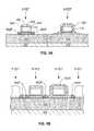
- FIGS. 9A-10Billustrate an exemplary method for fabricating complementary metal-oxide-semiconductors (CMOS) having both N-FETs and P-FETs fabricated on the same chip. Since N-FETs and P-FETs have nanowire extensions with different types of dopants, the N-FET device and P-FET device nanowire extensions are grown in separately.
- CMOScomplementary metal-oxide-semiconductors
- FIG. 9Billustrates a similar process as described in FIG. 9A for a plurality of N-FET and P-FET devices.
- the epi blocking masks 1001are removed, and a second epi blocking mask 1101 is deposited and patterned to cover the P-FET and the p+ doped nanowire extensions 902 P.
- Selective epitaxy with n-type in-situ dopingis used to form the n+ doped nanowire extensions 902 N.
- the second epi blocking mask 1101may be removed.
- the order by which the P-FET and N-FET nanowire extensions 902 are formedmay be chosen to minimize diffusion of dopants in the first grown extension during the growth of the second nanowire extension.
- the epitaxy of the n+ doped nanowire extensions 902 Nmay be formed prior to forming the p+ doped nanowire extensions 902 P. Since the formation of the nanowire extensions 902 may be carried out in separate processing steps, the extensions composition may be different. For example, SiGe nanowire extensions may be formed for the P-FET devices while pure silicon nanowire extensions may be formed for the N-FET devices.
- FIGS. 11A and 11Billustrate an example of the resultant structures following a thermal process (performed after the growth of the nanowire extensions 902 described above) that diffuses the doped ions from the nanowire extensions 902 into the regions 1202 of the nanowires 110 that are surrounded by the spacer walls 604 and the gates 404 to overlap the device.
- the nanowire extensions 902are uniformly doped when grown; resulting in a uniform doping profile in the regions 1202 of the nanowires 110 following diffusion of the ions from the nanowire extension 902 into the regions 1202 .
- CMOS devicesdescribed above in FIGS. 9A-10B
- a similar thermal processmay be performed.
- the thermal processmay be performed in a rapid thermal annealing (RTA) chamber.
- the thermal processmay be performed, for example, at annealing temperatures between 900° C. to 1100° C. for 0-10 seconds in an ambient N 2 gas.
- the annealing temperature ratemay range, for example, between 50° C./second to 300° C./second.
- FIGS. 12A and 12Billustrate a resultant structure following silicidation where a silicide 1302 is formed on the nanowires extensions 902 , and over the polysilicon layer 404 .
- silicide forming metalsinclude Ni, Pt, Co, and alloys such as NiPt. When Ni is used the NiSi phase is formed due to its low resistivity. For example, formation temperatures include 400-600° C.
- FIGS. 13A-14Billustrate an alternate exemplary method for forming a nanowire FET.
- the alternate exemplary methodis similar to the method described above in FIGS. 1-12B .
- the etching processremoves a portion of the nanowires 110 that are surrounded by the spacer walls 604 and the gates 402 to recess the nanowires 110 into the gates 402 , and form cavities 1402 defined by the gates 402 , the nanowires 110 and the spacer walls 604 .
- FIGS. 13A and 13Billustrate a cross-sectional view of the resultant structure.
- the lateral etching process that forms cavities 1402may be time based. Width variation in spacer 604 may lead to variations in the position of the edges of the recessed nanowires 110 .
- the etching rate in the cavity 1402depends on the size of the cavity, with narrower orifice corresponding to slower etch rates. Variations in the nanowire size will therefore lead to variations in the depth of cavity 1402 .
- the variations described abovemay be reduced by bombarding the exposed ends of nanowire 110 with ions (e.g. silicon ions, germanium ions, and even dopants such as boron which do not amorphize) prior to the formation of the spacer 604 (in FIGS. 5A and 5B ).
- ionse.g. silicon ions, germanium ions, and even dopants such as boron which do not amorphize
- the etching rate of the bombarded portions of nanowires 110is several times faster than that of the un-exposed portion of nanowire 110 protected by gate material 402 .
- the cavity 1402becomes self-aligned with the sidewalls of gate 402 when etched.
- the deposition processmay anneal the exposed nanowire 110 portions (that have been bombarded with ions) and increase the etching resistance of the exposed nanowire 110 portion.
- the spacer 604may be formed at a low temperature, for example, less than 500° C. to avoid annealing the bombarded portions of the nanowires 110 . If other materials are used to form the nanowires 110 are used, the formation temperature of the spacer 604 may be higher.
- An alternative that accommodates high temperature deposition of spacer 604includes performing an ion implantation at an oblique angle to the substrate 100 after the deposition of the spacer 604 with an ion energy that damages the portions of the nanowires 110 that are encapsulated by spacer 604 .
- FIGS. 14A and 14Ba cross-sectional view of the resultant structure having nanowire extensions 1502 that are formed from an in-situ doped epi-silicon growth process similar to the process described above in FIGS. 8A and 8B .
- the epi silicon growthbegan in the cavity 1402 (of FIGS. 13A and 13B ) from the exposed nanowire 110 in the gate 402 to form the nanowire extensions 1502 .
- the dopingmay be activated by, for example, a laser or flash anneal process.
- the laser or flash annealingmay reduce diffusion of ions into the channel region 1501 of the gate 402 , and result in a high uniform concentration of doping in the nanowire extensions 1502 with an abrupt junction in the nanowires 110 .
- silicidation similar to the process described in FIGS. 12A and 12B abovemay be performed and capping layers and vias for connectivity (not shown) may be formed.
Landscapes
- Engineering & Computer Science (AREA)
- Chemical & Material Sciences (AREA)
- Nanotechnology (AREA)
- Physics & Mathematics (AREA)
- Mathematical Physics (AREA)
- Theoretical Computer Science (AREA)
- Crystallography & Structural Chemistry (AREA)
- Thin Film Transistor (AREA)
- Insulated Gate Type Field-Effect Transistor (AREA)
Abstract
Description
Claims (18)
Priority Applications (1)
| Application Number | Priority Date | Filing Date | Title |
|---|---|---|---|
| US13/372,719US8680589B2 (en) | 2009-12-04 | 2012-02-14 | Omega shaped nanowire field effect transistors |
Applications Claiming Priority (2)
| Application Number | Priority Date | Filing Date | Title |
|---|---|---|---|
| US12/631,205US8129247B2 (en) | 2009-12-04 | 2009-12-04 | Omega shaped nanowire field effect transistors |
| US13/372,719US8680589B2 (en) | 2009-12-04 | 2012-02-14 | Omega shaped nanowire field effect transistors |
Related Parent Applications (1)
| Application Number | Title | Priority Date | Filing Date |
|---|---|---|---|
| US12/631,205DivisionUS8129247B2 (en) | 2009-12-04 | 2009-12-04 | Omega shaped nanowire field effect transistors |
Publications (2)
| Publication Number | Publication Date |
|---|---|
| US20120146000A1 US20120146000A1 (en) | 2012-06-14 |
| US8680589B2true US8680589B2 (en) | 2014-03-25 |
Family
ID=43127115
Family Applications (2)
| Application Number | Title | Priority Date | Filing Date |
|---|---|---|---|
| US12/631,205Expired - Fee RelatedUS8129247B2 (en) | 2009-12-04 | 2009-12-04 | Omega shaped nanowire field effect transistors |
| US13/372,719ActiveUS8680589B2 (en) | 2009-12-04 | 2012-02-14 | Omega shaped nanowire field effect transistors |
Family Applications Before (1)
| Application Number | Title | Priority Date | Filing Date |
|---|---|---|---|
| US12/631,205Expired - Fee RelatedUS8129247B2 (en) | 2009-12-04 | 2009-12-04 | Omega shaped nanowire field effect transistors |
Country Status (3)
| Country | Link |
|---|---|
| US (2) | US8129247B2 (en) |
| CN (1) | CN102640270B (en) |
| WO (1) | WO2011067069A1 (en) |
Families Citing this family (25)
| Publication number | Priority date | Publication date | Assignee | Title |
|---|---|---|---|---|
| US7884004B2 (en)* | 2009-02-04 | 2011-02-08 | International Business Machines Corporation | Maskless process for suspending and thinning nanowires |
| US8143113B2 (en)* | 2009-12-04 | 2012-03-27 | International Business Machines Corporation | Omega shaped nanowire tunnel field effect transistors fabrication |
| US8129247B2 (en) | 2009-12-04 | 2012-03-06 | International Business Machines Corporation | Omega shaped nanowire field effect transistors |
| US8455334B2 (en) | 2009-12-04 | 2013-06-04 | International Business Machines Corporation | Planar and nanowire field effect transistors |
| US8722492B2 (en) | 2010-01-08 | 2014-05-13 | International Business Machines Corporation | Nanowire pin tunnel field effect devices |
| US8324940B2 (en) | 2010-04-13 | 2012-12-04 | International Business Machines Corporation | Nanowire circuits in matched devices |
| US8361907B2 (en) | 2010-05-10 | 2013-01-29 | International Business Machines Corporation | Directionally etched nanowire field effect transistors |
| US8324030B2 (en) | 2010-05-12 | 2012-12-04 | International Business Machines Corporation | Nanowire tunnel field effect transistors |
| US8394710B2 (en)* | 2010-06-21 | 2013-03-12 | International Business Machines Corporation | Semiconductor devices fabricated by doped material layer as dopant source |
| US8835231B2 (en) | 2010-08-16 | 2014-09-16 | International Business Machines Corporation | Methods of forming contacts for nanowire field effect transistors |
| US8536563B2 (en) | 2010-09-17 | 2013-09-17 | International Business Machines Corporation | Nanowire field effect transistors |
| US20130026575A1 (en)* | 2011-07-28 | 2013-01-31 | Synopsys, Inc. | Threshold adjustment of transistors by controlled s/d underlap |
| US8648330B2 (en)* | 2012-01-05 | 2014-02-11 | International Business Machines Corporation | Nanowire field effect transistors |
| US8900959B2 (en) | 2013-03-12 | 2014-12-02 | International Business Machines Corporation | Non-replacement gate nanomesh field effect transistor with pad regions |
| KR102135303B1 (en) | 2013-12-27 | 2020-07-17 | 인텔 코포레이션 | Diffused tip extension transistor |
| US9263260B1 (en) | 2014-12-16 | 2016-02-16 | International Business Machines Corporation | Nanowire field effect transistor with inner and outer gates |
| CN105810730B (en)* | 2014-12-29 | 2018-12-07 | 中芯国际集成电路制造(上海)有限公司 | Semiconductor device and its manufacturing method |
| US10374086B2 (en)* | 2015-12-04 | 2019-08-06 | The Regents Of The University Of California | 3D transistor having a gate stack including a ferroelectric film |
| US10734511B2 (en)* | 2016-03-31 | 2020-08-04 | Intel Corporation | High mobility asymmetric field effect transistors with a band-offset semiconductor drain spacer |
| CN108695382B (en) | 2017-04-07 | 2021-07-06 | 中芯国际集成电路制造(上海)有限公司 | Semiconductor device and method of manufacturing the same |
| US10651291B2 (en) | 2017-08-18 | 2020-05-12 | Globalfoundries Inc. | Inner spacer formation in a nanosheet field-effect transistor |
| US10896956B2 (en)* | 2017-12-22 | 2021-01-19 | Commissariat A L'energie Atomique Et Aux Energies Alternatives | Field effect transistor with reduced contact resistance |
| US10686050B2 (en) | 2018-09-26 | 2020-06-16 | Taiwan Semiconductor Manufacturing Co., Ltd. | Method of manufacturing a semiconductor device and a semiconductor device |
| US11217694B2 (en)* | 2019-03-18 | 2022-01-04 | Shanghai Industrial Μtechnology Research Institute | Field-effect transistor and method for manufacturing the same |
| US10923348B2 (en)* | 2019-05-29 | 2021-02-16 | International Business Machines Corporation | Gate-all-around field effect transistor using template-assisted-slective-epitaxy |
Citations (90)
| Publication number | Priority date | Publication date | Assignee | Title |
|---|---|---|---|---|
| EP0217811A1 (en) | 1985-03-18 | 1987-04-15 | Caterpillar Inc | Engine having a multipiece cylinder block. |
| US4995001A (en) | 1988-10-31 | 1991-02-19 | International Business Machines Corporation | Memory cell and read circuit |
| US5308445A (en) | 1991-10-23 | 1994-05-03 | Rohm Co., Ltd. | Method of manufacturing a semiconductor device having a semiconductor growth layer completely insulated from a substrate |
| US5438018A (en) | 1992-12-07 | 1995-08-01 | Fujitsu Limited | Method of making semiconductor device by selective epitaxial growth |
| US5552622A (en) | 1992-07-14 | 1996-09-03 | Mitsuteru Kimura | Tunnel transistor |
| US5668046A (en) | 1991-03-27 | 1997-09-16 | Nec Corporation | Method of producing a semiconductor on insulating substrate, and a method of forming transistor thereon |
| US6365465B1 (en) | 1999-03-19 | 2002-04-02 | International Business Machines Corporation | Self-aligned double-gate MOSFET by selective epitaxy and silicon wafer bonding techniques |
| WO2002084757A1 (en) | 2001-04-12 | 2002-10-24 | Infineon Technologies Ag | Heterostructure component |
| US6642115B1 (en) | 2000-05-15 | 2003-11-04 | International Business Machines Corporation | Double-gate FET with planarized surfaces and self-aligned silicides |
| US6653209B1 (en) | 1999-09-30 | 2003-11-25 | Canon Kabushiki Kaisha | Method of producing silicon thin film, method of constructing SOI substrate and semiconductor device |
| US20040149978A1 (en) | 2003-01-31 | 2004-08-05 | Greg Snider | Molecular-junction-nanowire-crossbar-based inverter, latch, and flip-flop circuits, and more complex circuits composed, in part, from molecular-junction-nanowire-crossbar-based inverter, latch, and flip-flop circuits |
| US20040166642A1 (en) | 2003-02-20 | 2004-08-26 | Hao-Yu Chen | Semiconductor nano-rod devices |
| US6806141B2 (en) | 2002-05-22 | 2004-10-19 | Hewlett-Packard Development Company, L.P. | Field effect transistor with gate layer and method of making same |
| US6835618B1 (en)* | 2003-08-05 | 2004-12-28 | Advanced Micro Devices, Inc. | Epitaxially grown fin for FinFET |
| US6882051B2 (en) | 2001-03-30 | 2005-04-19 | The Regents Of The University Of California | Nanowires, nanostructures and devices fabricated therefrom |
| US6891227B2 (en) | 2002-03-20 | 2005-05-10 | International Business Machines Corporation | Self-aligned nanotube field effect transistor and method of fabricating same |
| US6903013B2 (en) | 2003-05-16 | 2005-06-07 | Chartered Semiconductor Manufacturing Ltd. | Method to fill a trench and tunnel by using ALD seed layer and electroless plating |
| US20050266645A1 (en) | 2004-05-25 | 2005-12-01 | Jin-Jun Park | Phosphorous doping methods of manufacturing field effect transistors having multiple stacked channels |
| US20050275010A1 (en) | 2004-06-10 | 2005-12-15 | Hung-Wei Chen | Semiconductor nano-wire devices and methods of fabrication |
| US20060033145A1 (en) | 2004-08-13 | 2006-02-16 | Ronald Kakoschke | Integrated memory device and process |
| US20060131665A1 (en)* | 2004-11-18 | 2006-06-22 | Murthy Anand S | Method for forming an integrated circuit |
| US20060138552A1 (en)* | 2004-09-30 | 2006-06-29 | Brask Justin K | Nonplanar transistors with metal gate electrodes |
| US7101762B2 (en) | 2000-07-07 | 2006-09-05 | International Business Machines Corporation | Self-aligned double gate mosfet with separate gates |
| US20060197164A1 (en) | 2003-10-24 | 2006-09-07 | Nick Lindert | Epitaxially deposited source/drain |
| US7151209B2 (en) | 2002-04-02 | 2006-12-19 | Nanosys, Inc. | Methods of making, positioning and orienting nanostructures, nanostructure arrays and nanostructure devices |
| US20070001219A1 (en) | 2005-06-30 | 2007-01-04 | Marko Radosavljevic | Block contact architectures for nanoscale channel transistors |
| US7180107B2 (en) | 2004-05-25 | 2007-02-20 | International Business Machines Corporation | Method of fabricating a tunneling nanotube field effect transistor |
| US7211853B2 (en) | 2001-07-26 | 2007-05-01 | Technische Universiteit Delft | Electronic device using carbon nanotubes |
| US7253060B2 (en) | 2004-06-08 | 2007-08-07 | Samsung Electronics Co., Ltd. | Gate-all-around type of semiconductor device and method of fabricating the same |
| US7297615B2 (en) | 2005-05-13 | 2007-11-20 | Samsung Electronics, Co., Ltd. | Si nanowire substrate, method of manufacturing the same, and method of manufacturing thin film transistor using the same |
| US20070267703A1 (en) | 2006-05-17 | 2007-11-22 | Chartered Semiconductor Manufacturing Ltd. | Strained channel transistor and method of fabrication thereof |
| US20070267619A1 (en) | 2006-05-22 | 2007-11-22 | Thomas Nirschl | Memory using tunneling field effect transistors |
| US20070284613A1 (en) | 2006-06-09 | 2007-12-13 | Chi On Chui | Strain-inducing semiconductor regions |
| US7311776B2 (en) | 2003-12-30 | 2007-12-25 | The Regents Of The University Of California | Localized synthesis and self-assembly of nanostructures |
| US20080014689A1 (en) | 2006-07-07 | 2008-01-17 | Texas Instruments Incorporated | Method for making planar nanowire surround gate mosfet |
| US20080061284A1 (en) | 2006-09-11 | 2008-03-13 | International Business Machines Corporation | Nanowire MOSFET with doped epitaxial contacts for source and drain |
| US20080067607A1 (en) | 2006-09-15 | 2008-03-20 | Interuniversitair Microelektronica Centrum (Imec) | Tunnel effect transistors based on elongate monocrystalline nanostructures having a heterostructure |
| US20080067495A1 (en) | 2006-09-15 | 2008-03-20 | Interuniversitair Microelektronica Centrum (Imec) | Tunnel effect transistors based on silicon nanowires |
| US20080079041A1 (en) | 2006-10-02 | 2008-04-03 | Samsung Electronics Co, Ltd. | Gate-all-around type semiconductor device and method of manufacturing the same |
| US20080085587A1 (en) | 2006-10-04 | 2008-04-10 | Micron Technology, Inc. | Epitaxial silicon growth |
| US20080121932A1 (en) | 2006-09-18 | 2008-05-29 | Pushkar Ranade | Active regions with compatible dielectric layers |
| US20080128760A1 (en) | 2006-12-04 | 2008-06-05 | Electronics And Telecommunications Research Institute | Schottky barrier nanowire field effect transistor and method for fabricating the same |
| WO2008069765A1 (en) | 2006-12-08 | 2008-06-12 | Agency For Science, Technology And Research | A stacked silicon-germanium nanowire structure and a method of forming the same |
| US20080142853A1 (en) | 2005-08-08 | 2008-06-19 | Freescale Semiconductor, Inc. | Multi-channel transistor structure and method of making thereof |
| US20080150025A1 (en) | 2005-12-13 | 2008-06-26 | Versatilis Llc | Methods of Making Semiconductor-Based Electronic Devices on a Wire and by Forming Freestanding Semiconductor Structures, and Devices That Can Be Made Thereby |
| US20080149997A1 (en) | 2006-12-20 | 2008-06-26 | Samsung Electronics Co., Ltd. | Nonvolatile memory device and method of operating the same |
| US20080149914A1 (en) | 2006-12-22 | 2008-06-26 | Qunano Ab | Nanoelectronic structure and method of producing such |
| US20080179752A1 (en) | 2007-01-26 | 2008-07-31 | Takashi Yamauchi | Method of making semiconductor device and semiconductor device |
| US20080191196A1 (en) | 2005-06-06 | 2008-08-14 | Wei Lu | Nanowire heterostructures |
| US20080224224A1 (en) | 2007-03-12 | 2008-09-18 | Interuniversitair Microelektronica Centrum Vzw (Imec) | Tunnel field-effect transistor with gated tunnel barrier |
| US20080227259A1 (en) | 2005-01-07 | 2008-09-18 | International Business Machines Corporation | SELF-ALIGNED PROCESS FOR NANOTUBE/NANOWIRE FETs |
| US20080247226A1 (en) | 2007-04-05 | 2008-10-09 | Micron Technology, Inc. | Memory devices having electrodes comprising nanowires, systems including same and methods of forming same |
| US20080246021A1 (en) | 2006-10-04 | 2008-10-09 | Samsung Electronic Co., Ltd., | Single electron transistor and method of manufacturing the same |
| US7443025B2 (en) | 2004-06-07 | 2008-10-28 | Broadcom Corporation | Thermally improved placement of power-dissipating components onto a circuit board |
| US7446025B2 (en) | 2005-05-23 | 2008-11-04 | International Business Machines Corporation | Method of forming vertical FET with nanowire channels and a silicided bottom contact |
| US7449373B2 (en) | 2006-03-31 | 2008-11-11 | Intel Corporation | Method of ion implanting for tri-gate devices |
| US7452759B2 (en) | 2005-11-29 | 2008-11-18 | Micron Technology, Inc. | Carbon nanotube field effect transistor and methods for making same |
| US7456068B2 (en) | 2006-06-08 | 2008-11-25 | Intel Corporation | Forming ultra-shallow junctions |
| US7456476B2 (en) | 2003-06-27 | 2008-11-25 | Intel Corporation | Nonplanar semiconductor device with partially or fully wrapped around gate electrode and methods of fabrication |
| US7473943B2 (en) | 2004-10-15 | 2009-01-06 | Nanosys, Inc. | Gate configuration for nanowire electronic devices |
| US20090026553A1 (en) | 2007-07-25 | 2009-01-29 | Krishna Kumar Bhuwalka | Tunnel Field-Effect Transistor with Narrow Band-Gap Channel and Strong Gate Coupling |
| US7498211B2 (en) | 2005-12-28 | 2009-03-03 | Intel Corporation | Independently controlled, double gate nanowire memory cell with self-aligned contacts |
| US20090057650A1 (en) | 2000-08-22 | 2009-03-05 | President And Fellows Of Harvard College | Nanoscale wires and related devices |
| US20090061568A1 (en) | 2007-09-05 | 2009-03-05 | International Business Machines Corporation | Techniques for Fabricating Nanowire Field-Effect Transistors |
| US20090057762A1 (en) | 2007-09-05 | 2009-03-05 | International Business Machines Corporation | Nanowire Field-Effect Transistors |
| US20090090934A1 (en) | 2007-10-05 | 2009-04-09 | Tsutomu Tezuka | Field Effect Transistor and Method for Manufacturing the Same |
| KR20090044799A (en) | 2007-11-01 | 2009-05-07 | 삼성전자주식회사 | Method for manufacturing active fin and transistor comprising same |
| US20090134467A1 (en) | 2007-11-26 | 2009-05-28 | Renesas Technology Corp. | Semiconductor device and a method of manufacturing the same |
| US7550333B2 (en) | 2004-10-25 | 2009-06-23 | Intel Corporation | Nonplanar device with thinned lower body portion and method of fabrication |
| US20090181477A1 (en) | 2005-07-01 | 2009-07-16 | Synopsys, Inc. | Integrated Circuit On Corrugated Substrate |
| US20090217216A1 (en) | 2007-02-28 | 2009-08-27 | Motorola, Inc. | Carbon nanotube circuits design methodology |
| US20090290418A1 (en) | 2008-05-20 | 2009-11-26 | Jung Chul Han | Method of verifying a program operation in a non-volatile memory device |
| US20090294864A1 (en) | 2005-06-13 | 2009-12-03 | Samsung Electronics Co., Ltd. | Mos field effect transistor having plurality of channels |
| US7642578B2 (en) | 2005-03-24 | 2010-01-05 | Samsung Electronics Co., Ltd. | Semiconductor device having a round-shaped nano-wire transistor channel and method of manufacturing same |
| US20100140589A1 (en) | 2008-12-04 | 2010-06-10 | Ecole Polytechnique Federale De Lausanne (Epfl) | Ferroelectric tunnel fet switch and memory |
| US20100193770A1 (en) | 2009-02-04 | 2010-08-05 | International Business Machines Corporation | Maskless Process for Suspending and Thinning Nanowires |
| US20100207102A1 (en) | 2009-02-18 | 2010-08-19 | Samsung Electronics Co., Ltd. | Static random access memories having carbon nanotube thin films |
| US7791144B2 (en) | 2006-04-28 | 2010-09-07 | International Business Machines Corporation | High performance stress-enhance MOSFET and method of manufacture |
| US7799657B2 (en) | 2005-06-07 | 2010-09-21 | Freescale Semiconductor, Inc. | Method of fabricating a substrate for a planar, double-gated, transistor process |
| US7834345B2 (en) | 2008-09-05 | 2010-11-16 | Taiwan Semiconductor Manufacturing Company, Ltd. | Tunnel field-effect transistors with superlattice channels |
| US7893506B2 (en) | 2005-02-23 | 2011-02-22 | Intel Corporation | Field effect transistor with narrow bandgap source and drain regions and method of fabrication |
| US20110133169A1 (en) | 2009-12-04 | 2011-06-09 | International Business Machines Corporation | Gate-All-Around Nanowire Tunnel Field Effect Transistors |
| US20110147840A1 (en) | 2009-12-23 | 2011-06-23 | Cea Stephen M | Wrap-around contacts for finfet and tri-gate devices |
| US8064249B2 (en) | 2006-09-11 | 2011-11-22 | Samsung Electronics Co., Ltd. | Nanowire electromechanical switching device, method of manufacturing the same and electromechanical memory device using the nanowire electromechanical switching device |
| US8097515B2 (en) | 2009-12-04 | 2012-01-17 | International Business Machines Corporation | Self-aligned contacts for nanowire field effect transistors |
| US8154127B1 (en) | 2007-07-30 | 2012-04-10 | Hewlett-Packard Development Company, L.P. | Optical device and method of making the same |
| US20120146000A1 (en) | 2009-12-04 | 2012-06-14 | International Business Machines Corporation | Omega Shaped Nanowire Field Effect Transistors |
| US8338280B2 (en) | 2010-07-08 | 2012-12-25 | Globalfoundries Singapore Pte. Ltd. | Method for fabricating nano devices |
| US20130001517A1 (en) | 2010-05-12 | 2013-01-03 | International Business Machines Corporation | Generation of multiple diameter nanowire field effect transistors |
| US8541774B2 (en) | 2011-07-25 | 2013-09-24 | International Business Machines Corporation | Hybrid CMOS technology with nanowire devices and double gated planar devices |
Family Cites Families (1)
| Publication number | Priority date | Publication date | Assignee | Title |
|---|---|---|---|---|
| US7871851B2 (en) | 2007-05-25 | 2011-01-18 | RF Nano | Method for integrating nanotube devices with CMOS for RF/analog SoC applications |
- 2009
- 2009-12-04USUS12/631,205patent/US8129247B2/ennot_activeExpired - Fee Related
- 2010
- 2010-11-08CNCN201080054741.8Apatent/CN102640270B/enactiveActive
- 2010-11-08WOPCT/EP2010/066961patent/WO2011067069A1/enactiveApplication Filing
- 2012
- 2012-02-14USUS13/372,719patent/US8680589B2/enactiveActive
Patent Citations (102)
| Publication number | Priority date | Publication date | Assignee | Title |
|---|---|---|---|---|
| EP0217811A1 (en) | 1985-03-18 | 1987-04-15 | Caterpillar Inc | Engine having a multipiece cylinder block. |
| US4995001A (en) | 1988-10-31 | 1991-02-19 | International Business Machines Corporation | Memory cell and read circuit |
| US5668046A (en) | 1991-03-27 | 1997-09-16 | Nec Corporation | Method of producing a semiconductor on insulating substrate, and a method of forming transistor thereon |
| US5308445A (en) | 1991-10-23 | 1994-05-03 | Rohm Co., Ltd. | Method of manufacturing a semiconductor device having a semiconductor growth layer completely insulated from a substrate |
| US5552622A (en) | 1992-07-14 | 1996-09-03 | Mitsuteru Kimura | Tunnel transistor |
| US5438018A (en) | 1992-12-07 | 1995-08-01 | Fujitsu Limited | Method of making semiconductor device by selective epitaxial growth |
| US5574308A (en) | 1992-12-07 | 1996-11-12 | Fujitsu Limited | Semiconductor device and its manufacturing method |
| US6365465B1 (en) | 1999-03-19 | 2002-04-02 | International Business Machines Corporation | Self-aligned double-gate MOSFET by selective epitaxy and silicon wafer bonding techniques |
| US6653209B1 (en) | 1999-09-30 | 2003-11-25 | Canon Kabushiki Kaisha | Method of producing silicon thin film, method of constructing SOI substrate and semiconductor device |
| US6642115B1 (en) | 2000-05-15 | 2003-11-04 | International Business Machines Corporation | Double-gate FET with planarized surfaces and self-aligned silicides |
| US7101762B2 (en) | 2000-07-07 | 2006-09-05 | International Business Machines Corporation | Self-aligned double gate mosfet with separate gates |
| US20090057650A1 (en) | 2000-08-22 | 2009-03-05 | President And Fellows Of Harvard College | Nanoscale wires and related devices |
| US7569941B2 (en) | 2001-03-30 | 2009-08-04 | The Regents Of The University Of California | Methods of fabricating nanostructures and nanowires and devices fabricated therefrom |
| US6882051B2 (en) | 2001-03-30 | 2005-04-19 | The Regents Of The University Of California | Nanowires, nanostructures and devices fabricated therefrom |
| US6996147B2 (en) | 2001-03-30 | 2006-02-07 | The Regents Of The University Of California | Methods of fabricating nanostructures and nanowires and devices fabricated therefrom |
| WO2002084757A1 (en) | 2001-04-12 | 2002-10-24 | Infineon Technologies Ag | Heterostructure component |
| US7211853B2 (en) | 2001-07-26 | 2007-05-01 | Technische Universiteit Delft | Electronic device using carbon nanotubes |
| US6891227B2 (en) | 2002-03-20 | 2005-05-10 | International Business Machines Corporation | Self-aligned nanotube field effect transistor and method of fabricating same |
| US7151209B2 (en) | 2002-04-02 | 2006-12-19 | Nanosys, Inc. | Methods of making, positioning and orienting nanostructures, nanostructure arrays and nanostructure devices |
| US6806141B2 (en) | 2002-05-22 | 2004-10-19 | Hewlett-Packard Development Company, L.P. | Field effect transistor with gate layer and method of making same |
| US20040149978A1 (en) | 2003-01-31 | 2004-08-05 | Greg Snider | Molecular-junction-nanowire-crossbar-based inverter, latch, and flip-flop circuits, and more complex circuits composed, in part, from molecular-junction-nanowire-crossbar-based inverter, latch, and flip-flop circuits |
| US20040166642A1 (en) | 2003-02-20 | 2004-08-26 | Hao-Yu Chen | Semiconductor nano-rod devices |
| US20050121706A1 (en)* | 2003-02-20 | 2005-06-09 | Hao-Yu Chen | Semiconductor nano-rod devices |
| US6855606B2 (en) | 2003-02-20 | 2005-02-15 | Taiwan Semiconductor Manufacturing Company, Ltd. | Semiconductor nano-rod devices |
| US6903013B2 (en) | 2003-05-16 | 2005-06-07 | Chartered Semiconductor Manufacturing Ltd. | Method to fill a trench and tunnel by using ALD seed layer and electroless plating |
| US7456476B2 (en) | 2003-06-27 | 2008-11-25 | Intel Corporation | Nonplanar semiconductor device with partially or fully wrapped around gate electrode and methods of fabrication |
| US6835618B1 (en)* | 2003-08-05 | 2004-12-28 | Advanced Micro Devices, Inc. | Epitaxially grown fin for FinFET |
| US20060197164A1 (en) | 2003-10-24 | 2006-09-07 | Nick Lindert | Epitaxially deposited source/drain |
| US7311776B2 (en) | 2003-12-30 | 2007-12-25 | The Regents Of The University Of California | Localized synthesis and self-assembly of nanostructures |
| US20050266645A1 (en) | 2004-05-25 | 2005-12-01 | Jin-Jun Park | Phosphorous doping methods of manufacturing field effect transistors having multiple stacked channels |
| US7180107B2 (en) | 2004-05-25 | 2007-02-20 | International Business Machines Corporation | Method of fabricating a tunneling nanotube field effect transistor |
| US7443025B2 (en) | 2004-06-07 | 2008-10-28 | Broadcom Corporation | Thermally improved placement of power-dissipating components onto a circuit board |
| US7253060B2 (en) | 2004-06-08 | 2007-08-07 | Samsung Electronics Co., Ltd. | Gate-all-around type of semiconductor device and method of fabricating the same |
| US20050275010A1 (en) | 2004-06-10 | 2005-12-15 | Hung-Wei Chen | Semiconductor nano-wire devices and methods of fabrication |
| US7452778B2 (en) | 2004-06-10 | 2008-11-18 | Taiwan Semiconductor Manufacturing Company, Ltd. | Semiconductor nano-wire devices and methods of fabrication |
| US20060033145A1 (en) | 2004-08-13 | 2006-02-16 | Ronald Kakoschke | Integrated memory device and process |
| US20060138552A1 (en)* | 2004-09-30 | 2006-06-29 | Brask Justin K | Nonplanar transistors with metal gate electrodes |
| US20090149012A1 (en) | 2004-09-30 | 2009-06-11 | Brask Justin K | Method of forming a nonplanar transistor with sidewall spacers |
| US7871870B2 (en) | 2004-10-15 | 2011-01-18 | Nanosys, Inc. | Method of fabricating gate configurations for an improved contacts in nanowire based electronic devices |
| US7473943B2 (en) | 2004-10-15 | 2009-01-06 | Nanosys, Inc. | Gate configuration for nanowire electronic devices |
| US7550333B2 (en) | 2004-10-25 | 2009-06-23 | Intel Corporation | Nonplanar device with thinned lower body portion and method of fabrication |
| US20060131665A1 (en)* | 2004-11-18 | 2006-06-22 | Murthy Anand S | Method for forming an integrated circuit |
| US20080227259A1 (en) | 2005-01-07 | 2008-09-18 | International Business Machines Corporation | SELF-ALIGNED PROCESS FOR NANOTUBE/NANOWIRE FETs |
| US7893506B2 (en) | 2005-02-23 | 2011-02-22 | Intel Corporation | Field effect transistor with narrow bandgap source and drain regions and method of fabrication |
| US7642578B2 (en) | 2005-03-24 | 2010-01-05 | Samsung Electronics Co., Ltd. | Semiconductor device having a round-shaped nano-wire transistor channel and method of manufacturing same |
| US7297615B2 (en) | 2005-05-13 | 2007-11-20 | Samsung Electronics, Co., Ltd. | Si nanowire substrate, method of manufacturing the same, and method of manufacturing thin film transistor using the same |
| US7446025B2 (en) | 2005-05-23 | 2008-11-04 | International Business Machines Corporation | Method of forming vertical FET with nanowire channels and a silicided bottom contact |
| US20080191196A1 (en) | 2005-06-06 | 2008-08-14 | Wei Lu | Nanowire heterostructures |
| US7799657B2 (en) | 2005-06-07 | 2010-09-21 | Freescale Semiconductor, Inc. | Method of fabricating a substrate for a planar, double-gated, transistor process |
| US20090294864A1 (en) | 2005-06-13 | 2009-12-03 | Samsung Electronics Co., Ltd. | Mos field effect transistor having plurality of channels |
| US20070001219A1 (en) | 2005-06-30 | 2007-01-04 | Marko Radosavljevic | Block contact architectures for nanoscale channel transistors |
| US20090181477A1 (en) | 2005-07-01 | 2009-07-16 | Synopsys, Inc. | Integrated Circuit On Corrugated Substrate |
| US20080142853A1 (en) | 2005-08-08 | 2008-06-19 | Freescale Semiconductor, Inc. | Multi-channel transistor structure and method of making thereof |
| US7452759B2 (en) | 2005-11-29 | 2008-11-18 | Micron Technology, Inc. | Carbon nanotube field effect transistor and methods for making same |
| US20080150025A1 (en) | 2005-12-13 | 2008-06-26 | Versatilis Llc | Methods of Making Semiconductor-Based Electronic Devices on a Wire and by Forming Freestanding Semiconductor Structures, and Devices That Can Be Made Thereby |
| US7498211B2 (en) | 2005-12-28 | 2009-03-03 | Intel Corporation | Independently controlled, double gate nanowire memory cell with self-aligned contacts |
| US7449373B2 (en) | 2006-03-31 | 2008-11-11 | Intel Corporation | Method of ion implanting for tri-gate devices |
| US7791144B2 (en) | 2006-04-28 | 2010-09-07 | International Business Machines Corporation | High performance stress-enhance MOSFET and method of manufacture |
| US20070267703A1 (en) | 2006-05-17 | 2007-11-22 | Chartered Semiconductor Manufacturing Ltd. | Strained channel transistor and method of fabrication thereof |
| US20070267619A1 (en) | 2006-05-22 | 2007-11-22 | Thomas Nirschl | Memory using tunneling field effect transistors |
| US7456068B2 (en) | 2006-06-08 | 2008-11-25 | Intel Corporation | Forming ultra-shallow junctions |
| US20070284613A1 (en) | 2006-06-09 | 2007-12-13 | Chi On Chui | Strain-inducing semiconductor regions |
| US20080014689A1 (en) | 2006-07-07 | 2008-01-17 | Texas Instruments Incorporated | Method for making planar nanowire surround gate mosfet |
| US20080061284A1 (en) | 2006-09-11 | 2008-03-13 | International Business Machines Corporation | Nanowire MOSFET with doped epitaxial contacts for source and drain |
| US8064249B2 (en) | 2006-09-11 | 2011-11-22 | Samsung Electronics Co., Ltd. | Nanowire electromechanical switching device, method of manufacturing the same and electromechanical memory device using the nanowire electromechanical switching device |
| US20080067495A1 (en) | 2006-09-15 | 2008-03-20 | Interuniversitair Microelektronica Centrum (Imec) | Tunnel effect transistors based on silicon nanowires |
| US20080067607A1 (en) | 2006-09-15 | 2008-03-20 | Interuniversitair Microelektronica Centrum (Imec) | Tunnel effect transistors based on elongate monocrystalline nanostructures having a heterostructure |
| US20080121932A1 (en) | 2006-09-18 | 2008-05-29 | Pushkar Ranade | Active regions with compatible dielectric layers |
| US20080079041A1 (en) | 2006-10-02 | 2008-04-03 | Samsung Electronics Co, Ltd. | Gate-all-around type semiconductor device and method of manufacturing the same |
| US7803675B2 (en) | 2006-10-02 | 2010-09-28 | Samsung Electronics Co., Ltd. | Gate-all-around type semiconductor device and method of manufacturing the same |
| US20080246021A1 (en) | 2006-10-04 | 2008-10-09 | Samsung Electronic Co., Ltd., | Single electron transistor and method of manufacturing the same |
| US20080085587A1 (en) | 2006-10-04 | 2008-04-10 | Micron Technology, Inc. | Epitaxial silicon growth |
| US20080128760A1 (en) | 2006-12-04 | 2008-06-05 | Electronics And Telecommunications Research Institute | Schottky barrier nanowire field effect transistor and method for fabricating the same |
| WO2008069765A1 (en) | 2006-12-08 | 2008-06-12 | Agency For Science, Technology And Research | A stacked silicon-germanium nanowire structure and a method of forming the same |
| US20080135949A1 (en) | 2006-12-08 | 2008-06-12 | Agency For Science, Technology And Research | Stacked silicon-germanium nanowire structure and method of forming the same |
| US20080149997A1 (en) | 2006-12-20 | 2008-06-26 | Samsung Electronics Co., Ltd. | Nonvolatile memory device and method of operating the same |
| US20080149914A1 (en) | 2006-12-22 | 2008-06-26 | Qunano Ab | Nanoelectronic structure and method of producing such |
| US20080179752A1 (en) | 2007-01-26 | 2008-07-31 | Takashi Yamauchi | Method of making semiconductor device and semiconductor device |
| US20090217216A1 (en) | 2007-02-28 | 2009-08-27 | Motorola, Inc. | Carbon nanotube circuits design methodology |
| US20080224224A1 (en) | 2007-03-12 | 2008-09-18 | Interuniversitair Microelektronica Centrum Vzw (Imec) | Tunnel field-effect transistor with gated tunnel barrier |
| US20080247226A1 (en) | 2007-04-05 | 2008-10-09 | Micron Technology, Inc. | Memory devices having electrodes comprising nanowires, systems including same and methods of forming same |
| US20090026553A1 (en) | 2007-07-25 | 2009-01-29 | Krishna Kumar Bhuwalka | Tunnel Field-Effect Transistor with Narrow Band-Gap Channel and Strong Gate Coupling |
| US8154127B1 (en) | 2007-07-30 | 2012-04-10 | Hewlett-Packard Development Company, L.P. | Optical device and method of making the same |
| US7795677B2 (en) | 2007-09-05 | 2010-09-14 | International Business Machines Corporation | Nanowire field-effect transistors |
| US7534675B2 (en) | 2007-09-05 | 2009-05-19 | International Business Machiens Corporation | Techniques for fabricating nanowire field-effect transistors |
| US20090061568A1 (en) | 2007-09-05 | 2009-03-05 | International Business Machines Corporation | Techniques for Fabricating Nanowire Field-Effect Transistors |
| US20090057762A1 (en) | 2007-09-05 | 2009-03-05 | International Business Machines Corporation | Nanowire Field-Effect Transistors |
| US20090090934A1 (en) | 2007-10-05 | 2009-04-09 | Tsutomu Tezuka | Field Effect Transistor and Method for Manufacturing the Same |
| KR20090044799A (en) | 2007-11-01 | 2009-05-07 | 삼성전자주식회사 | Method for manufacturing active fin and transistor comprising same |
| US20090134467A1 (en) | 2007-11-26 | 2009-05-28 | Renesas Technology Corp. | Semiconductor device and a method of manufacturing the same |
| US20090290418A1 (en) | 2008-05-20 | 2009-11-26 | Jung Chul Han | Method of verifying a program operation in a non-volatile memory device |
| US7834345B2 (en) | 2008-09-05 | 2010-11-16 | Taiwan Semiconductor Manufacturing Company, Ltd. | Tunnel field-effect transistors with superlattice channels |
| US20100140589A1 (en) | 2008-12-04 | 2010-06-10 | Ecole Polytechnique Federale De Lausanne (Epfl) | Ferroelectric tunnel fet switch and memory |
| US20100193770A1 (en) | 2009-02-04 | 2010-08-05 | International Business Machines Corporation | Maskless Process for Suspending and Thinning Nanowires |
| US20100207102A1 (en) | 2009-02-18 | 2010-08-19 | Samsung Electronics Co., Ltd. | Static random access memories having carbon nanotube thin films |
| US20110133169A1 (en) | 2009-12-04 | 2011-06-09 | International Business Machines Corporation | Gate-All-Around Nanowire Tunnel Field Effect Transistors |
| US8097515B2 (en) | 2009-12-04 | 2012-01-17 | International Business Machines Corporation | Self-aligned contacts for nanowire field effect transistors |
| US20120146000A1 (en) | 2009-12-04 | 2012-06-14 | International Business Machines Corporation | Omega Shaped Nanowire Field Effect Transistors |
| US20110147840A1 (en) | 2009-12-23 | 2011-06-23 | Cea Stephen M | Wrap-around contacts for finfet and tri-gate devices |
| US20130001517A1 (en) | 2010-05-12 | 2013-01-03 | International Business Machines Corporation | Generation of multiple diameter nanowire field effect transistors |
| US8338280B2 (en) | 2010-07-08 | 2012-12-25 | Globalfoundries Singapore Pte. Ltd. | Method for fabricating nano devices |
| US8541774B2 (en) | 2011-07-25 | 2013-09-24 | International Business Machines Corporation | Hybrid CMOS technology with nanowire devices and double gated planar devices |
Non-Patent Citations (58)
| Title |
|---|
| Alexander J. Gates, "Designing a Nanoelectronic Circuit to Control a Millimeter-scale Walking Robot," Mitre Technical Paper, Nov. 2004, http://www.mitre.org/work/tech-papers/tech-papers-04/04-1248/04-1248.pdf. |
| Andriotis et al., 'Realistic nanotube-metal contact configuration for molecular electronics applications, IEEE Sensors Journal, vol. 8, No. 6, Jun. 2008. |
| Buddharaju et al., 'Gate-All-Around Si-Nanowire CMOS Inverter Logic Fabricated Using Top-Down Approach', European Solid-State Device Research Conference, Sep. 11-11, 2007, pp. 303-306. |
| Checka, N., 'Circuit Architecture for 3D Integration', Chapter 13 in Wafer Level 3-D ICs Process Technology, ed. C.S. Tan, Springer US, 2008, ISBN 978-0-387-76534-1. |
| Chen et al., "An Integrated Logic Circuit Assembled ona Single Carbon Nanotube", www.sciencemag.org Science, vol. 311, Mar. 24, 2006, p. 1735. |
| Chen et al., 'Demonstration of Tunneling FETs Based on Highly Scalable Verticle Silicon Nanowires', IEEE Electron Device Letters, vol. 30, No. 7, Jul. 2009, pp. 754-756. |
| Derycke, et al, "Carbon Nanotube Inter- and Intramolecular Logic Gates" Nano Letters, Sep. 2001, vol. 1, No. 9, pp. 453-456. |
| Ernst et al., "3D Multichannels and Stacked Nanowires Technologies for New Design Opportunities in Nanoelectronics," IEEE International Conference on Integrated Circuit Design and Technology and Tutorial, 2008. ICICDT 2008. Jun. 2-4, 2008 pp. 265-268. |
| G.W. Neudeck, "An Overview of Double-Gate MOSFETs," Proceedings of 15th Biennial University/Government/Industry Microelectronics Symposium. UGIM 2003. New York, NY: IEEE, US, Jun. 30-Jul. 2, 2003, Jun. 30, 2003, pp. 214-217. |
| Hu et al., 'Fringing field effects on electrical resistivity of semiconductor nanowire-metal contacts', Applied Physics Letters 92, 083503-2008. |
| International Search Report Written Opinion; International Application No. PCT/US11/49501; International Filing Date: Aug. 29, 2011; Date of Mailing: Jan. 18, 2012. |
| International Search Report; International Application No. PCT/EP2010/066483; International Filing Date: Oct. 29, 2010; Date of Mailing: Feb. 7, 2011. |
| International Search Report; International Application No. PCT/EP2010/066961; International Filing Date: Nov. 8, 2010; Date of Mailing: Feb. 10, 2011. |
| International Search Report; International Application No. PCT/EP2011/053174; International Filing Date: Mar. 3, 2011; Date of Mailing: May 31, 2011. |
| International Search Report; International Application No. PCT/US11/49501; International Filing Date: Aug. 29, 2011; Date of Mailing: Jan. 18, 2012. |
| International Search Report; International Application No. PCT/US2011/029304; International Filing Date: Mar. 22, 2011; Date of Mailing: May 20, 2011. |
| International Search Report-Written Opinion; International Application No. PCT/EP2010/066483; International Filing Date: Oct. 29, 2010; Date of Mailing: Feb. 7, 2011. |
| International Search Report-Written Opinion; International Application No. PCT/EP2010/066961; International Filing Date: Nov. 8, 2010; Date of Mailing: Feb. 10, 2011. |
| International Search Report-Written Opinion; International Application No. PCT/EP2011/053174; International Filing Date: Mar. 3, 2011; Date of Mailing: May 31, 2011. |
| International Search Report-Written Opinion; International Application No. PCT/US2011/029304; International Filing Date: Mar. 22, 2011; Date of Mailing; May 20, 2011. |
| Jie Xiang et al., "Ge/Si Nanowire Heterostructures as High-Performance Field-Effect Transistors," Nature 441, 489-493 (May 25, 2006). |
| Knoch et al., 'Tunneling phenomena in carbon nanotube field-effect transistors', Phys Stat Sol. (a) 205, No. 4, 679-694 (2008). |
| Lauhon et al., 'Epitaxial core-shell and core-multishell nanowire heterostructures', Nature, vol. 420, Nov. 7, 2002, pp. 57-61. |
| Leonard et al., 'Size-dependent effects on electrical contacts to nanotubes and nanowires', Phys Rev Lett., Jul. 14, 2006; 97(2):026804. |
| M. M. Ziegler et al., "The CMOS/NANO Interface from a Circuits Perspective," ISCAS '03. Proceedings of the 2003 International Symposium on Circuits and Systems, 2003, May 25-28, 2003, vol. 4, pp. IV-904-IV-907. |
| M. T. Bjork et al., "Silicon Nanowire Tunneling Field-Effect Transistors," Applied Physics Letters 92, 193504 (2008). |
| Ma et al., 'High-performance nanowire complementary metal-semiconductor inverters', Applied Physics Letters 93, 053105-2008. |
| N. Checka, 'Circuit Architecture for 3D Integration', Chapter 13 in Wafer Level 3-D ICs Process Technology, ed. C.S. Tan, Springer US, 2008, ISBN 978-0-387-76534-1. |
| Notice of Allowance for U.S. Appl. No. 12/776,485, filed May 10, 2010; First Named Inventor: Sarunya Bangsaruntip; Mailing Date: Sep. 26, 2012. |
| Office Action-Final for U.S. Appl. No. 12/684,280, filed Jan. 8, 2010; First Named Inventor: Sarunya Bangsaruntip; Mailing Date: Oct. 5, 2011. |
| Office Action-Final for U.S. Appl. No. 12/856,718, filed Aug. 16, 2010; First Named Inventor: Sarunya Bangsaruntip; Mailing Date: Dec. 13, 2012. |
| Office Action-Final for U.S. Appl. No. 13/551,995, filed Jul. 18, 2012; First Named Inventor: Sarunya Bangsaruntip; Mailing Date Apr. 30, 2013, 11 pgs. |
| Office Action-Non-Final for U.S. Appl. No. 12/631,199, filed Dec. 4, 2009; First Named Inventor: Sarunya Bangsaruntip; Mailing Date: Jun. 13, 2012. |
| Office Action-Non-Final for U.S. Appl. No. 12/684,280, filed Jan. 8, 2010; First Named Inventor: Sarunya Bangsaruntip; Mailing Date: May 2, 2011. |
| Office Action-Non-Final for U.S. Appl. No. 12/776,485, filed May 10, 2010; First Named Inventor: Sarunya Bangsaruntip; Mailing Date: Feb. 21, 2012. |
| Office Action-Non-Final for U.S. Appl. No. 12/778,315, filed May 12, 2010; First Named Inventor: Sarunya Bangsaruntip; Mailing Date: Mar. 26, 2012. |
| Office Action-Non-Final for U.S. Appl. No. 12/856,718, filed Aug. 16, 2010; first Named Inventor Sarunya Bangsaruntip; Mailing Date: Jul. 9, 2012. |
| Office Action-Non-Final for U.S. Appl. No. 12/856,718, filed Aug. 16, 2010; First Named Inventor: Sarunya Bangsaruntip; Mailing Date: Jul. 9, 2012. |
| Office Action-Non-Final for U.S. Appl. No. 12/884,707, filed Sep. 17, 2010; First Named Inventor: Sarunya Bangsaruntip et al; Mailing Date: Oct. 2, 2012. |
| Office Action-Non-Final for U.S. Appl. No. 13/372,714, filed Feb. 14, 2012; First Named Inventor: Sarunya Bangsaruntip et al; Mailing Date: Sep. 20, 2012. |
| Office Action-Non-Final for U.S. Appl. No. 13/372,719, filed Feb. 14, 2012; First Named Inventor: Sarunya Bangsaruntip; Mailing Date: Sep. 4, 2012. |
| Office Action-Non-Final for U.S. Appl. No. 13/550,700, filed Jul. 17, 2012; First Named Inventor: Sarunya Bangsaruntip; Mailing Date: Apr. 25, 2013, 27 pgs. |
| Office Action-Non-Final for U.S. Appl. No. 13/550,700, filed Jul. 17, 2012; First Named Inventor: Sarunya Bangsaruntip; Mailing Date: Apr. 25, 2013; 27 pgs. |
| Office Action-Non-Final for U.S. Appl. No. 13/551,995, filed Jul. 18, 2012; First Named Inventor: Sarunya Bangsaruntip; Mailing Date: Dec. 19, 2012. |
| Office Action-Non-Final for U.S. Appl. No. 13/556,300, filed Jul. 24, 2012; First Named Inventor: Sarunya Bangsaruntip; Mailing Date: Dec. 10, 2012. |
| Office Action-Non-Final for U.S. Appl. No. 13/600,585, filed Aug. 31, 2012; First Named Inventor: Sarunya Bangsaruntip; Mailing Date: Dec. 13, 2012. |
| Office Action-Notice of Allowance for U.S. Appl. No. 13/551,995, filed Jul. 18, 2012; First Named Inventtor: Sarunya Bangsaruntip; Mailing Date: Jul. 15, 2013; 13 pages. |
| Office Action-Restriction Election for U.S. Appl. No. 12/684,280, filed Jan. 8, 2010; First Named Inventor: Sarunya Bangsaruntip; Mailing Date: Feb. 10, 2011. |
| Office Action-Restriction Election for U.S. Appl. No. 12/776,485, filed May 10, 2010; First Named Inventor: Sarunya Bangsaruntip; Mailing Date: Dec. 9, 2011. |
| Office Action-Restriction-Election for U.S. Appl. No. 12/856,718, filed Aug. 16, 2010; First Named Inventor: Sarunya Bangsaruntip; Mailing Date: Apr. 9, 2012. |
| Pavanello et al., "Evaluation of Triple-Gate FinFETs With SiO2-HfO2--TiN Gate Stack Under Analog Operation," Solid State Electronics, Elsevier Science Publishers, Barking, GB, vol. 51, No. 2, Mar. 7, 2007, pp. 285-291. |
| R, Bahar, 'Trends and Future Directions in Nano Structure Based Computing and Fabrication', ICCD 2006, International Conf. on Computer Design, Oct. 1-4, 2007, pp. 522-527. |
| Restriction/Election Office Action for U.S. Appl. No. 12/758,939, filed Apr. 13, 2010; First Named Inventor: Sarunya Bangsaruntip; Mailing Date: Jun. 8, 2012. |
| Saumitra Raj Mehrotra, 'A Simulation Study of Silicom Nanowire Field Effect Transistors (FETs), University of Cincinnati, Jul. 2007. |
| Singh et al., 'High-Performance Fully Depleted Silicon Nanowire (Diameter = 5 nm) Gatw-All-Around CMOS Devices', IEEE Electron Device Letters, vol. 27, No. 5, May 2006, pp. 383-386. |
| Taichi Su et al., "New Planar Self-Aligned Double-Gate Fully Depleted P-MOSFET's Using Epitaxial Lateral Overgrowth (ELO) and Selectively Grown Source/Drain (S/D)," 2000 IEEE International SOI Conference, Oct. 2000, pp. 110-111. |
| Transmittal and International Preliminary Report on Patentability for International Application No. PCT/US2011/029304; International Filing Date: Mar. 22, 2011; date of mailing Oct. 26, 2012, 2 pages. |
| Written Opinion for International Application No. PCT/US2011/029304; International Filing Date: Mar. 22, 2011; mailing date: May 20, 2011; 5 pages. |
Also Published As
| Publication number | Publication date |
|---|---|
| CN102640270B (en) | 2015-08-12 |
| CN102640270A (en) | 2012-08-15 |
| US20110133164A1 (en) | 2011-06-09 |
| US8129247B2 (en) | 2012-03-06 |
| WO2011067069A1 (en) | 2011-06-09 |
| US20120146000A1 (en) | 2012-06-14 |
Similar Documents
| Publication | Publication Date | Title |
|---|---|---|
| US8680589B2 (en) | Omega shaped nanowire field effect transistors | |
| US8384065B2 (en) | Gate-all-around nanowire field effect transistors | |
| US8674342B2 (en) | Pad-less gate-all around semiconductor nanowire FETs on bulk semiconductor wafers | |
| US8097515B2 (en) | Self-aligned contacts for nanowire field effect transistors | |
| US8173993B2 (en) | Gate-all-around nanowire tunnel field effect transistors | |
| US8143113B2 (en) | Omega shaped nanowire tunnel field effect transistors fabrication | |
| US8455334B2 (en) | Planar and nanowire field effect transistors | |
| US7332439B2 (en) | Metal gate transistors with epitaxial source and drain regions | |
| US8324030B2 (en) | Nanowire tunnel field effect transistors | |
| US8835231B2 (en) | Methods of forming contacts for nanowire field effect transistors | |
| US8361895B2 (en) | Ultra-shallow junctions using atomic-layer doping | |
| US7759205B1 (en) | Methods for fabricating semiconductor devices minimizing under-oxide regrowth | |
| US8722492B2 (en) | Nanowire pin tunnel field effect devices | |
| JP2010505267A (en) | Stress application field effect transistor and method of manufacturing the same | |
| CN102598229A (en) | Bi-layer nfet embedded stressor element and integration to enhance drive current | |
| US9331174B2 (en) | Method for improving device performance using epitaxially grown silicon carbon (SiC) or silicon-germanium (SiGe) | |
| US8563385B2 (en) | Field effect transistor device with raised active regions |
Legal Events
| Date | Code | Title | Description |
|---|---|---|---|
| STCF | Information on status: patent grant | Free format text:PATENTED CASE | |
| AS | Assignment | Owner name:GLOBALFOUNDRIES U.S. 2 LLC, NEW YORK Free format text:ASSIGNMENT OF ASSIGNORS INTEREST;ASSIGNOR:INTERNATIONAL BUSINESS MACHINES CORPORATION;REEL/FRAME:036550/0001 Effective date:20150629 | |
| AS | Assignment | Owner name:GLOBALFOUNDRIES INC., CAYMAN ISLANDS Free format text:ASSIGNMENT OF ASSIGNORS INTEREST;ASSIGNORS:GLOBALFOUNDRIES U.S. 2 LLC;GLOBALFOUNDRIES U.S. INC.;REEL/FRAME:036779/0001 Effective date:20150910 | |
| MAFP | Maintenance fee payment | Free format text:PAYMENT OF MAINTENANCE FEE, 4TH YEAR, LARGE ENTITY (ORIGINAL EVENT CODE: M1551) Year of fee payment:4 | |
| AS | Assignment | Owner name:WILMINGTON TRUST, NATIONAL ASSOCIATION, DELAWARE Free format text:SECURITY AGREEMENT;ASSIGNOR:GLOBALFOUNDRIES INC.;REEL/FRAME:049490/0001 Effective date:20181127 | |
| AS | Assignment | Owner name:GLOBALFOUNDRIES U.S. INC., CALIFORNIA Free format text:ASSIGNMENT OF ASSIGNORS INTEREST;ASSIGNOR:GLOBALFOUNDRIES INC.;REEL/FRAME:054633/0001 Effective date:20201022 | |
| AS | Assignment | Owner name:GLOBALFOUNDRIES INC., CAYMAN ISLANDS Free format text:RELEASE BY SECURED PARTY;ASSIGNOR:WILMINGTON TRUST, NATIONAL ASSOCIATION;REEL/FRAME:054636/0001 Effective date:20201117 | |
| AS | Assignment | Owner name:GLOBALFOUNDRIES U.S. INC., NEW YORK Free format text:RELEASE BY SECURED PARTY;ASSIGNOR:WILMINGTON TRUST, NATIONAL ASSOCIATION;REEL/FRAME:056987/0001 Effective date:20201117 | |
| MAFP | Maintenance fee payment | Free format text:PAYMENT OF MAINTENANCE FEE, 8TH YEAR, LARGE ENTITY (ORIGINAL EVENT CODE: M1552); ENTITY STATUS OF PATENT OWNER: LARGE ENTITY Year of fee payment:8 | |
| MAFP | Maintenance fee payment | Free format text:PAYMENT OF MAINTENANCE FEE, 12TH YEAR, LARGE ENTITY (ORIGINAL EVENT CODE: M1553); ENTITY STATUS OF PATENT OWNER: LARGE ENTITY Year of fee payment:12 |