US8676116B2 - Electronic device with NFC antenna adjacent display and related methods - Google Patents
Electronic device with NFC antenna adjacent display and related methodsDownload PDFInfo
- Publication number
- US8676116B2 US8676116B2US13/269,054US201113269054AUS8676116B2US 8676116 B2US8676116 B2US 8676116B2US 201113269054 AUS201113269054 AUS 201113269054AUS 8676116 B2US8676116 B2US 8676116B2
- Authority
- US
- United States
- Prior art keywords
- housing
- display
- nfc
- transceiver circuitry
- circuitry
- Prior art date
- Legal status (The legal status is an assumption and is not a legal conclusion. Google has not performed a legal analysis and makes no representation as to the accuracy of the status listed.)
- Active, expires
Links
Images


Classifications
- H—ELECTRICITY
- H04—ELECTRIC COMMUNICATION TECHNIQUE
- H04M—TELEPHONIC COMMUNICATION
- H04M1/00—Substation equipment, e.g. for use by subscribers
- H04M1/02—Constructional features of telephone sets
- H04M1/0202—Portable telephone sets, e.g. cordless phones, mobile phones or bar type handsets
- H04M1/026—Details of the structure or mounting of specific components
- H—ELECTRICITY
- H01—ELECTRIC ELEMENTS
- H01Q—ANTENNAS, i.e. RADIO AERIALS
- H01Q1/00—Details of, or arrangements associated with, antennas
- H01Q1/12—Supports; Mounting means
- H01Q1/22—Supports; Mounting means by structural association with other equipment or articles
- H01Q1/24—Supports; Mounting means by structural association with other equipment or articles with receiving set
- H01Q1/241—Supports; Mounting means by structural association with other equipment or articles with receiving set used in mobile communications, e.g. GSM
- H01Q1/242—Supports; Mounting means by structural association with other equipment or articles with receiving set used in mobile communications, e.g. GSM specially adapted for hand-held use
- H01Q1/243—Supports; Mounting means by structural association with other equipment or articles with receiving set used in mobile communications, e.g. GSM specially adapted for hand-held use with built-in antennas
- H—ELECTRICITY
- H01—ELECTRIC ELEMENTS
- H01Q—ANTENNAS, i.e. RADIO AERIALS
- H01Q1/00—Details of, or arrangements associated with, antennas
- H01Q1/52—Means for reducing coupling between antennas; Means for reducing coupling between an antenna and another structure
- H01Q1/526—Electromagnetic shields
- H—ELECTRICITY
- H01—ELECTRIC ELEMENTS
- H01Q—ANTENNAS, i.e. RADIO AERIALS
- H01Q21/00—Antenna arrays or systems
- H01Q21/28—Combinations of substantially independent non-interacting antenna units or systems
- H—ELECTRICITY
- H01—ELECTRIC ELEMENTS
- H01Q—ANTENNAS, i.e. RADIO AERIALS
- H01Q7/00—Loop antennas with a substantially uniform current distribution around the loop and having a directional radiation pattern in a plane perpendicular to the plane of the loop
- H—ELECTRICITY
- H04—ELECTRIC COMMUNICATION TECHNIQUE
- H04B—TRANSMISSION
- H04B1/00—Details of transmission systems, not covered by a single one of groups H04B3/00 - H04B13/00; Details of transmission systems not characterised by the medium used for transmission
- H04B1/38—Transceivers, i.e. devices in which transmitter and receiver form a structural unit and in which at least one part is used for functions of transmitting and receiving
- H04B1/3827—Portable transceivers
- H04B1/3888—Arrangements for carrying or protecting transceivers
- H—ELECTRICITY
- H04—ELECTRIC COMMUNICATION TECHNIQUE
- H04B—TRANSMISSION
- H04B5/00—Near-field transmission systems, e.g. inductive or capacitive transmission systems
- H04B5/20—Near-field transmission systems, e.g. inductive or capacitive transmission systems characterised by the transmission technique; characterised by the transmission medium
- H04B5/24—Inductive coupling
- H04B5/26—Inductive coupling using coils
- H—ELECTRICITY
- H04—ELECTRIC COMMUNICATION TECHNIQUE
- H04M—TELEPHONIC COMMUNICATION
- H04M1/00—Substation equipment, e.g. for use by subscribers
- H04M1/02—Constructional features of telephone sets
- H04M1/0202—Portable telephone sets, e.g. cordless phones, mobile phones or bar type handsets
- H04M1/026—Details of the structure or mounting of specific components
- H04M1/0266—Details of the structure or mounting of specific components for a display module assembly
- H—ELECTRICITY
- H04—ELECTRIC COMMUNICATION TECHNIQUE
- H04M—TELEPHONIC COMMUNICATION
- H04M2250/00—Details of telephonic subscriber devices
- H04M2250/04—Details of telephonic subscriber devices including near field communication means, e.g. RFID
- H—ELECTRICITY
- H04—ELECTRIC COMMUNICATION TECHNIQUE
- H04M—TELEPHONIC COMMUNICATION
- H04M2250/00—Details of telephonic subscriber devices
- H04M2250/22—Details of telephonic subscriber devices including a touch pad, a touch sensor or a touch detector
- Y—GENERAL TAGGING OF NEW TECHNOLOGICAL DEVELOPMENTS; GENERAL TAGGING OF CROSS-SECTIONAL TECHNOLOGIES SPANNING OVER SEVERAL SECTIONS OF THE IPC; TECHNICAL SUBJECTS COVERED BY FORMER USPC CROSS-REFERENCE ART COLLECTIONS [XRACs] AND DIGESTS
- Y10—TECHNICAL SUBJECTS COVERED BY FORMER USPC
- Y10T—TECHNICAL SUBJECTS COVERED BY FORMER US CLASSIFICATION
- Y10T29/00—Metal working
- Y10T29/49—Method of mechanical manufacture
- Y10T29/49002—Electrical device making
- Y10T29/49016—Antenna or wave energy "plumbing" making
- Y10T29/49018—Antenna or wave energy "plumbing" making with other electrical component
Definitions
- the present inventionrelates to the field of wireless communications, and, more particularly, to mobile wireless communications and related methods.
- PDAPersonal Digital Assistant
- NECnear field communication
- NFC antennaIn some mobile applications where size and packaging are limited, it may be difficult to place an NFC antenna effectively since the typical NFC antenna relies on magnetic induction. In particular, other nearby components may cause interference and reduce the operational efficiency of the NFC antenna.
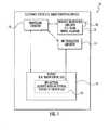
- FIG. 1is a schematic diagram of an electronic device, according to the present disclosure.
- FIG. 2is a top side view of an example embodiment of the display from the electronic device of FIG. 1 .
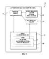
- FIG. 3is a schematic diagram of another embodiment of the electronic device, according to the present disclosure.
- FIG. 4is a top side view of an example embodiment of the frame from the electronic device of FIG. 3 .
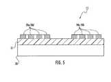
- FIG. 5is a cross-sectional view along line 5 - 5 of the NFC antenna from the display of FIG. 2 .
- FIG. 6is a schematic block diagram illustrating example components of a mobile wireless communications device that may be used with the electronic device of FIG. 1 .
- an electronic devicefor example, a tablet computer or a mobile phone device, may include a housing having a display opening therein, processing circuitry within the housing, and wireless transceiver circuitry within the housing and coupled to the processing circuitry.
- the electronic devicemay also include NFC transceiver circuitry within the housing and coupled to the processing circuitry, and a display within the housing and coupled to the processing circuitry.
- the displaymay have an external surface exposed through the display opening and have an internal surface within the housing.
- the electronic devicealso may include an NFC antenna positioned within the housing behind and aligned with the internal surface of the display and coupled to the NFC transceiver circuitry.
- the NFC antennamay comprise a substrate and electrically conductive traces thereon defining a plurality of loops.
- the substratemay have a rectangular shape, the plurality of loops being adjacent a periphery of the substrate.
- the electronic devicemay further comprise a flexible circuit coupling the NFC antenna to the NFC transceiver circuitry.
- the substratemay comprise a ferrite layer.
- the electronic devicemay further comprise a frame within the housing and behind the internal surface of the display, and the NFC antenna may be mounted on the frame.
- the NFC antennamay be mounted to the internal surface of the display.
- the displaymay comprise a touch screen display, for example.
- the wireless transceiver circuitrymay comprise at least one of cellular transceiver circuitry, WiMAX transceiver circuitry, and wireless local area network (WLAN) transceiver circuitry.
- the processing circuitrymay comprise tablet computer processing circuitry.
- the methodmay comprise forming a housing having a display opening therein, coupling processing circuitry within the housing, and coupling wireless transceiver circuitry within the housing and to the processing circuitry.
- the methodmay further comprise coupling NFC transceiver circuitry within the housing and to the processing circuitry, and coupling a display within the housing and to the processing circuitry.
- the displaymay have an external surface exposed through the display opening and an internal surface within the housing.
- the methodalso may comprise positioning an NFC antenna within the housing behind and aligned with the internal surface of the display, and coupling the NFC antenna to the NFC transceiver circuitry.
- Example mobile wireless communications devicesmay include portable or personal media players (e.g., music or MP3 players, video players, etc.), remote controls (e.g., television or stereo remotes, etc.), portable gaming devices, portable or mobile telephones, smartphones, tablet computers, etc.
- portable or personal media playerse.g., music or MP3 players, video players, etc.
- remote controlse.g., television or stereo remotes, etc.
- portable gaming devicesportable or mobile telephones, smartphones, tablet computers, etc.
- NFCis a short-range wireless communications technology in which NFC-enabled devices are “swiped,” “bumped” or otherwise moved in close proximity to communicate.
- NFCmay operate at 13.56 MHz and with an effective range of about 10 cm, but other suitable versions of near-field communication which may have different operating frequencies, effective ranges, etc., for example, may also be used.
- the electronic device 10illustratively includes a housing 11 having a display opening therein, processing circuitry 12 within the housing, and wireless transceiver circuitry 13 within the housing and coupled to the processing circuitry.
- the electronic device 10illustratively includes an antenna 38 coupled to the wireless transceiver circuitry 13 .
- the wireless transceiver circuitry 13may comprise at least one of cellular transceiver circuitry, WiMAX transceiver circuitry, and WLAN transceiver circuitry.
- the electronic device 10illustratively includes NFC transceiver circuitry 14 within the housing 11 and coupled to the processing circuitry 12 , and a display 16 within the housing and coupled to the processing circuitry.
- the display 16illustratively includes an external surface exposed through the display opening and an internal surface within the housing 11 .
- the display 16may include a touch screen with a user input surface facing outward though the display opening.
- the electronic device 10illustratively includes an NFC antenna 15 (shown with dashed lines in FIG. 1 ) positioned within the housing 11 behind and aligned with the internal surface (i.e. external surface) of the display 16 and coupled to the NFC transceiver circuitry 14 .
- the NFC antenna 15illustratively includes a backing layer 30 , a substrate 21 on the backing layer, and electrically conductive traces 20 a - 20 h thereon defining a plurality of loops.
- the substrate 21illustratively includes a rectangular shape, the plurality of loops being adjacent a periphery of the substrate.
- the backing layer 30may comprise ferrite and may provide some inductive shielding for the NFC antenna 15 .
- the display 16illustratively includes an internal surface 35 .
- the NFC antenna 15is directly mounted on the internal surface 35 .
- the electronic device 10illustratively includes a flexible circuit 17 coupling the NFC antenna 15 to the NFC transceiver circuitry.
- the display 16illustratively includes a plurality of foot portions 23 a - 23 d for coupling to the housing 11 .
- fastening devicessuch as screws, can be used to secure the display 16 to the housing 11 .
- the electronic device 10 ′illustratively includes a frame 24 ′ (shown with dashed lines in FIG. 3 ) within the housing 11 ′ and behind the internal surface of the display 16 ′.
- the NFC antenna 15 ′is mounted on the frame 24 ′, which is fastened to the display 16 ′.
- the frame 24 ′illustratively includes a plurality of foot portions 33 a ′- 33 d ′ for coupling to the display 11 ′.
- the frame 24 ′also illustratively includes a plurality of connectors 27 a ′- 27 c ′ for permitting external connections to the electronic device 10 ′.
- the positioning of the NFC antenna 15provides for improved performance, as noted in Table 1.
- the NFC antenna 15 of the present applicationprovides improved reading range.
- the LCD and touch screenespecially LCD
- the size of NFC antenna 15e.g. 50 mm ⁇ 42 mm.
- number of turns of the antennae.g. 50 mm ⁇ 42 mm.
- the “best” trade-off of antenna Q and inductanceis obtained, in order to achieve better operating volume of both NFC reader and card emulation modes.
- the metal influence on the back of NFC antennamay be reduced to achieve the best Q factor and inductance of the NFC antenna 15 .
- Table 1highlights the reader and card emulation modes of operation of 2-turn NFC antenna 15 .
- Types Names Protocol FormFactor(NO. 1) (NO. 2) Type 1 Topaz ISO 14443 A-2 ID1 96b 25 25 Square 96b 18 22 ID1 512b 18 20 Type 2 Mifare ISO 14443 A-3 ID1 15 14 Ultralight Circular ⁇ 2.5 11 10 Type 5 Picopass ISO 14443 B-3 Square 4.5 cm 20 21 ID1 14 13 Type 3 Felica Felica ID1 27 26 Icode 15-3 ID1 38 37 Detection Range (mm) 2 turns (NO. 1) 2 turns (NO. 2) Vivotech 5000 reader ON 30 32 OFF 18 17
- the device 1000illustratively includes a housing 1200 , a keyboard or keypad 1400 and an output device 1600 .
- the output device shownis a display 1600 , which may comprise a full graphic liquid crystal display (LCD). Other types of output devices may alternatively be utilized.
- a processing device 1800is contained within the housing 1200 and is coupled between the keypad 1400 and the display 1600 . The processing device 1800 controls the operation of the display 1600 , as well as the overall operation of the mobile device 1000 , in response to actuation of keys on the keypad 1400 .
- the housing 1200may be elongated vertically, or may take on other sizes and shapes (including clamshell housing structures).
- the keypadmay include a mode selection key, or other hardware or software for switching between text entry and telephony entry.
- FIG. 11In addition to the processing device 1800 , other parts of the mobile device 1000 are shown schematically in FIG. 11 . These include a communications subsystem 1001 ; a short-range communications subsystem 1020 ; the keypad 1400 and the display 1600 , along with other input/output devices 1060 , 1080 , 1100 and 1120 ; as well as memory devices 1160 , 1180 and various other device subsystems 1201 .
- the mobile device 1000may comprise a two-way RF communications device having data and, optionally, voice communications capabilities. In addition, the mobile device 1000 may have the capability to communicate with other computer systems via the Internet.
- Operating system software executed by the processing device 1800is stored in a persistent store, such as the flash memory 1160 , but may be stored in other types of memory devices, such as a read only memory (ROM) or similar storage element.
- system software, specific device applications, or parts thereofmay be temporarily loaded into a volatile store, such as the random access memory (RAM) 1180 .
- Communications signals received by the mobile devicemay also be stored in the RAM 1180 .
- the processing device 1800in addition to its operating system functions, enables execution of software applications 1300 A- 1300 N on the device 1000 .
- a predetermined set of applications that control basic device operations, such as data and voice communications 1300 A and 1300 B,may be installed on the device 1000 during manufacture.
- a personal information manager (PIM) applicationmay be installed during manufacture.
- the PIMmay be capable of organizing and managing data items, such as e-mail, calendar events, voice mails, appointments, and task items.
- the PIM applicationmay also be capable of sending and receiving data items via a wireless network 1401 .
- the PIM data itemsmay be seamlessly integrated, synchronized and updated via the wireless network 1401 with corresponding data items stored or associated with a host computer system.
- the communications subsystem 1001includes a receiver 1500 , a transmitter 1520 , and one or more antennas 1540 and 1560 .
- the communications subsystem 1001also includes a processing module, such as a digital signal, processor (DSP) 1580 , and local oscillators (LOs) 1601 .
- DSPdigital signal, processor
- LOslocal oscillators
- a mobile device 1000may include a communications subsystem 1001 designed to operate with the MobitexTM, Data TACTM or General Packet Radio Service (GPRS) mobile data communications networks, and also designed to operate with any of a variety of voice communications networks, such as Advanced Mobile Phone System (AMPS), time division multiple access (TDMA), code division multiple access (CDMA), Wideband code division multiple access (W-CDMA), personal communications service (PCS), GSM (Global System for Mobile Communications), enhanced data rates for GSM evolution (EDGE), etc.
- AMPSAdvanced Mobile Phone System
- TDMAtime division multiple access
- CDMAcode division multiple access
- W-CDMAWideband code division multiple access
- PCSpersonal communications service
- GSMGlobal System for Mobile Communications
- EDGEenhanced data rates for GSM evolution
- Other types of data and voice networks, both separate and integrated,may also be utilized with the mobile device 1000 .
- the mobile device 1000may also be compliant with other communications standards such as 3GSM, 3rd Generation Partnership Project (3GPP), Universal Mobile Telecommunication
- Network access requirementsvary depending upon the type of communication system. For example, in the Mobitex and DataTAC networks, mobile devices are registered on the network using a unique personal identification number or PIN associated with each device. In GPRS networks, however, network access is associated with a subscriber or user of a device. A GPRS device therefore typically involves use of a subscriber identity module, commonly referred to as a SIM card, in order to operate on a GPRS network.
- SIM cardsubscriber identity module
- the mobile device 1000may send and receive communications signals over the communication network 1401 .
- Signals received from the communications network 1401 by the antenna 1540are routed to the receiver 1500 , which provides for signal amplification, frequency down conversion, filtering, channel selection, etc., and may also provide analog to digital conversion. Analog-to-digital conversion of the received signal allows the DSP 1580 to perform more complex communications functions, such as demodulation and decoding.
- signals to be transmitted to the network 1401are processed (e.g. modulated and encoded) by the DSP 1580 and are then provided to the transmitter 1520 for digital to analog conversion, frequency up conversion, filtering, amplification and transmission to the communication network 1401 (or networks) via the antenna 1560 .
- the DSP 1580provides for control of the receiver 1500 and the transmitter 1520 .
- gains applied to communications signals in the receiver 1500 and transmitter 1520may be adaptively controlled through automatic gain control algorithms implemented in the DSP 1580 .
- a received signalsuch as a text message or web page download
- the communications subsystem 1001is input to the processing device 1800 .
- the received signalis then further processed by the processing device 1800 for an output to the display 1600 , or alternatively to some other auxiliary I/O device 1060 .
- a devicemay also be used to compose data items, such as e-mail messages, using the keypad 1400 and/or some other auxiliary I/O device 1060 , such as a touchpad, a rocker switch, a thumb-wheel, or some other type of input device.
- the composed data itemsmay then be transmitted over the communications network 1401 via the communications subsystem 1001 .
- a voice communications modeIn a voice communications mode, overall operation of the device is substantially similar to the data communications mode, except that received signals are output to a speaker 1100 , and signals for transmission are generated by a microphone 1120 .
- Alternative voice or audio I/O subsystemssuch as a voice message recording subsystem, may also be implemented on the device 1000 .
- the display 1600may also be utilized in voice communications mode, for example to display the identity of a calling party, the duration of a voice call, or other voice call related information.
- the short-range communications subsystemenables communication between the mobile device 1000 and other proximate systems or devices, which need not necessarily be similar devices.
- the short-range communications subsystemmay include an infrared device and associated circuits and components, a BluetoothTM communications module to provide for communication with similarly-enabled systems and devices, or a NFC sensor for communicating with a NFC device or NFC tag via NFC communications.
Landscapes
- Engineering & Computer Science (AREA)
- Signal Processing (AREA)
- Computer Networks & Wireless Communication (AREA)
- Physics & Mathematics (AREA)
- Electromagnetism (AREA)
- Telephone Set Structure (AREA)
- Mobile Radio Communication Systems (AREA)
- Support Of Aerials (AREA)
- Transceivers (AREA)
Abstract
Description
| TABLE 1 |
| Reading Range (mm) |
| Tag | Tag | 2 turns | 2 turns | |||
| Types | Names | Protocol | FormFactor | (NO. 1) | (NO. 2) | |
| Topaz | ISO 14443 | ID1 96b | 25 | 25 | ||
| Square 96b | 18 | 22 | ||||
| ID1 512b | 18 | 20 | ||||
| Type 2 | Mifare | ISO 14443 | ID1 | 15 | 14 | |
| Ultralight | Circular ø2.5 | 11 | 10 | |||
| Picopass | ISO 14443 B-3 | Square 4.5 | 20 | 21 | ||
| 14 | 13 | |||||
| Type 3 | Felica | Felica | ID1 | 27 | 26 | |
| Icode | 15-3 | 38 | 37 | |||
| Detection Range (mm) |
| 2 turns (NO. 1) | 2 turns (NO. 2) | ||
| Vivotech 5000 reader | ON | 30 | 32 |
| OFF | 18 | 17 | |
Claims (24)
Priority Applications (5)
| Application Number | Priority Date | Filing Date | Title |
|---|---|---|---|
| US13/269,054US8676116B2 (en) | 2011-10-07 | 2011-10-07 | Electronic device with NFC antenna adjacent display and related methods |
| CA2791514ACA2791514C (en) | 2011-10-07 | 2012-10-04 | Electronic device with nfc antenna adjacent display and related methods |
| EP12187459.8AEP2579388B1 (en) | 2011-10-07 | 2012-10-05 | Electronic device with NFC antenna adjacent display and related methods |
| US14/164,962US9609096B2 (en) | 2011-10-07 | 2014-01-27 | Electronic device with NFC antenna adjacent display and related methods |
| US15/432,979US10623540B2 (en) | 2011-10-07 | 2017-02-15 | Electronic device with NFC antenna adjacent display and related methods |
Applications Claiming Priority (1)
| Application Number | Priority Date | Filing Date | Title |
|---|---|---|---|
| US13/269,054US8676116B2 (en) | 2011-10-07 | 2011-10-07 | Electronic device with NFC antenna adjacent display and related methods |
Related Child Applications (1)
| Application Number | Title | Priority Date | Filing Date |
|---|---|---|---|
| US14/164,962ContinuationUS9609096B2 (en) | 2011-10-07 | 2014-01-27 | Electronic device with NFC antenna adjacent display and related methods |
Publications (2)
| Publication Number | Publication Date |
|---|---|
| US20130090073A1 US20130090073A1 (en) | 2013-04-11 |
| US8676116B2true US8676116B2 (en) | 2014-03-18 |
Family
ID=45002689
Family Applications (3)
| Application Number | Title | Priority Date | Filing Date |
|---|---|---|---|
| US13/269,054Active2032-03-29US8676116B2 (en) | 2011-10-07 | 2011-10-07 | Electronic device with NFC antenna adjacent display and related methods |
| US14/164,962Active2031-10-13US9609096B2 (en) | 2011-10-07 | 2014-01-27 | Electronic device with NFC antenna adjacent display and related methods |
| US15/432,979ActiveUS10623540B2 (en) | 2011-10-07 | 2017-02-15 | Electronic device with NFC antenna adjacent display and related methods |
Family Applications After (2)
| Application Number | Title | Priority Date | Filing Date |
|---|---|---|---|
| US14/164,962Active2031-10-13US9609096B2 (en) | 2011-10-07 | 2014-01-27 | Electronic device with NFC antenna adjacent display and related methods |
| US15/432,979ActiveUS10623540B2 (en) | 2011-10-07 | 2017-02-15 | Electronic device with NFC antenna adjacent display and related methods |
Country Status (3)
| Country | Link |
|---|---|
| US (3) | US8676116B2 (en) |
| EP (1) | EP2579388B1 (en) |
| CA (1) | CA2791514C (en) |
Cited By (4)
| Publication number | Priority date | Publication date | Assignee | Title |
|---|---|---|---|---|
| US20120099023A1 (en)* | 2010-10-25 | 2012-04-26 | Hyoung-Sik Nam | Display device and system for wirelessly transmitting/receiving image signals |
| US20140141835A1 (en)* | 2011-10-07 | 2014-05-22 | Blackberry Limited | Electronic device with nfc antenna adjacent display and related methods |
| US20140187153A1 (en)* | 2013-01-03 | 2014-07-03 | Research In Motion Limited | Mobile wireless communications device including nfc antenna matching control circuit and associated methods |
| US10320067B2 (en) | 2016-01-26 | 2019-06-11 | Samsung Electronics Co., Ltd. | Device and method for performing communication |
Families Citing this family (23)
| Publication number | Priority date | Publication date | Assignee | Title |
|---|---|---|---|---|
| US10020847B2 (en)* | 2011-11-15 | 2018-07-10 | Famoco | NFC device and connection system of NFC devices |
| WO2013072435A1 (en)* | 2011-11-15 | 2013-05-23 | Famoco | Nfc device and connection system of nfc devices |
| US9740342B2 (en)* | 2011-12-23 | 2017-08-22 | Cirque Corporation | Method for preventing interference of contactless card reader and touch functions when they are physically and logically bound together for improved authentication security |
| US9268420B2 (en)* | 2012-03-05 | 2016-02-23 | Htc Corporation | Touch panel structure and touch display panel structure having antenna pattern and related communications device having such touch panel structure |
| CN102737582B (en)* | 2012-04-06 | 2014-07-09 | 信利工业(汕尾)有限公司 | Termination point (TP) On/In Cell type organic electroluminescent display integrated with near field communication (NFC) antenna |
| US9262651B2 (en) | 2013-01-08 | 2016-02-16 | Cirque Corporation | Method for preventing unintended contactless interaction when performing contact interaction |
| US9620843B2 (en)* | 2013-01-31 | 2017-04-11 | Hewlett-Packard Development Company, L.P. | Display panel for front-side wireless communication |
| GB2517421B (en)* | 2013-08-19 | 2020-09-02 | Arm Ip Ltd | A layered display unit with antenna for a wrist worn device |
| US9363476B2 (en)* | 2013-09-20 | 2016-06-07 | Microsoft Technology Licensing, Llc | Configuration of a touch screen display with conferencing |
| US20150085060A1 (en) | 2013-09-20 | 2015-03-26 | Microsoft Corporation | User experience for conferencing with a touch screen display |
| KR20150094394A (en)* | 2014-02-11 | 2015-08-19 | 삼성전자주식회사 | User device and data swap control method thereof |
| US9591175B2 (en) | 2014-11-02 | 2017-03-07 | Clover Network, Inc. | Connecting a printer and a mobile device using identification information printed by the printer |
| US9319029B1 (en) | 2015-06-19 | 2016-04-19 | Clover Network, Inc. | System and method for automatic filter tuning |
| US9513756B1 (en) | 2015-08-28 | 2016-12-06 | Clover Network, Inc. | Providing near field communication through a touch screen |
| US9942367B2 (en)* | 2015-10-13 | 2018-04-10 | Samsung Electronics Co., Ltd. | Electronic device and method for controlling the electronic device thereof |
| KR102362535B1 (en) | 2015-10-27 | 2022-02-15 | 삼성전자주식회사 | Apparatus and method for managementing interference in an wireless communication system |
| CN107483658A (en)* | 2017-07-05 | 2017-12-15 | 深圳市橙方智能科技有限公司 | Intelligent terminal and combined, extended back splint |
| WO2021043199A1 (en) | 2019-09-04 | 2021-03-11 | Oppo广东移动通信有限公司 | Nfc antenna used for mobile terminal, and nfc communication apparatus |
| CN111083258B (en)* | 2019-12-20 | 2024-10-11 | 上海摩勤智能技术有限公司 | NFC screen module and electronic terminal |
| CN113540788B (en)* | 2020-04-17 | 2022-09-27 | 荣耀终端有限公司 | Electronic device |
| CN113675582A (en)* | 2020-05-15 | 2021-11-19 | 威速达(苏州)电子有限公司昆山分公司 | Touch control assembly with near field communication circuit |
| GB202014141D0 (en)* | 2020-09-09 | 2020-10-21 | Ifpl Group Ltd | Contactless reader |
| CN116243759B (en)* | 2021-12-08 | 2024-04-02 | 荣耀终端有限公司 | An NFC communication method, electronic device, storage medium and program product |
Citations (9)
| Publication number | Priority date | Publication date | Assignee | Title |
|---|---|---|---|---|
| US7202825B2 (en) | 2005-09-15 | 2007-04-10 | Motorola, Inc. | Wireless communication device with integrated battery/antenna system |
| US20080081631A1 (en) | 2006-09-29 | 2008-04-03 | Ahmadreza Rofougaran | Method And System For Integrating An NFC Antenna And A BT/WLAN Antenna |
| US7825860B2 (en) | 2008-04-16 | 2010-11-02 | Sony Ericsson Mobile Communications Ab | Antenna assembly |
| US20100315389A1 (en)* | 2009-06-12 | 2010-12-16 | Qualcomm Incorporated | Devices and methods related to a display assembly including an antenna |
| US7917115B2 (en) | 2007-03-19 | 2011-03-29 | Broadcom Corporation | Method and system for auto detecting and auto switching antennas in a multi-antenna FM transmit/receive system |
| US20110111720A1 (en) | 2009-10-13 | 2011-05-12 | Research In Motion Limited (a corporation organized under the laws of Province of | Mobile wireless device with multi feed point antenna and audio transducer and related methods |
| US20110111814A1 (en) | 2009-10-13 | 2011-05-12 | Research In Motion Limited | Mobile wireless device with integrated antenna and audio transducer assembly and related methods |
| US20110111719A1 (en) | 2009-10-13 | 2011-05-12 | Research In Motion Limited | Mobile wireless device with multi-layer flex antenna and related methods |
| US7973722B1 (en)* | 2007-08-28 | 2011-07-05 | Apple Inc. | Electronic device with conductive housing and near field antenna |
Family Cites Families (25)
| Publication number | Priority date | Publication date | Assignee | Title |
|---|---|---|---|---|
| US6962613B2 (en)* | 2000-03-24 | 2005-11-08 | Cymbet Corporation | Low-temperature fabrication of thin-film energy-storage devices |
| SE523191C2 (en)* | 2000-09-25 | 2004-03-30 | Ericsson Telefon Ab L M | A portable communication device with a first and a second antenna, the radiating portion of the first antenna being integrated with a display in a multilayer structure |
| JP2003179678A (en)* | 2001-10-03 | 2003-06-27 | Nec Corp | Portable telephone |
| JP4534854B2 (en)* | 2005-04-26 | 2010-09-01 | ソニー株式会社 | Information processing system, information processing apparatus and method, and program |
| JP4036228B2 (en)* | 2005-06-20 | 2008-01-23 | 船井電機株式会社 | Liquid crystal display |
| US7769345B2 (en)* | 2006-09-29 | 2010-08-03 | Sony Ericsson Mobile Communications Ab | Device and method for guiding a user to a communication position |
| CN101321195B (en)* | 2007-06-08 | 2011-11-16 | 深圳富泰宏精密工业有限公司 | Portable electronic device |
| KR101225838B1 (en)* | 2007-07-12 | 2013-01-23 | 애플 인크. | Methods for integrally trapping a glass insert in a metal bezel and produced electronic device |
| US8456381B2 (en)* | 2008-03-31 | 2013-06-04 | Intel Corporation | Device, system, and method of providing an extended display with desired relative display orientation |
| US9106275B2 (en)* | 2009-09-24 | 2015-08-11 | Blackberry Limited | Accelerometer tap detection to initiate NFC communication |
| US9677555B2 (en)* | 2011-12-21 | 2017-06-13 | Deka Products Limited Partnership | System, method, and apparatus for infusing fluid |
| KR101139096B1 (en) | 2010-12-08 | 2012-04-30 | 에스케이씨앤씨 주식회사 | Payment method using display apparatus having antenna for contactless reader |
| CN102783041B (en)* | 2010-12-28 | 2015-04-15 | 松下电器(美国)知识产权公司 | Communication device and communication method |
| TWI557986B (en)* | 2011-05-10 | 2016-11-11 | 群邁通訊股份有限公司 | Portable electronic device with nfc function |
| US9246219B2 (en)* | 2011-07-07 | 2016-01-26 | Htc Corporation | Handheld device |
| US8676116B2 (en)* | 2011-10-07 | 2014-03-18 | Blackberry Limited | Electronic device with NFC antenna adjacent display and related methods |
| US8660612B2 (en)* | 2011-10-07 | 2014-02-25 | Blackberry Limited | Electronic device having an NFC antenna in a speaker compartment and related methods |
| US9706036B2 (en)* | 2011-12-05 | 2017-07-11 | Blackberry Limited | Mobile wireless communications device providing guide direction indicator for near field communication (NFC) initiation and related methods |
| US9740342B2 (en)* | 2011-12-23 | 2017-08-22 | Cirque Corporation | Method for preventing interference of contactless card reader and touch functions when they are physically and logically bound together for improved authentication security |
| US9641239B2 (en)* | 2012-06-22 | 2017-05-02 | Fitbit, Inc. | Adaptive data transfer using bluetooth |
| US9225388B2 (en)* | 2012-07-03 | 2015-12-29 | Intel Corporation | Transmitting magnetic field through metal chassis using fractal surfaces |
| US8989670B2 (en)* | 2012-09-24 | 2015-03-24 | Intel Corporation | Location aware file sharing between near field communication enabled devices |
| TW201426220A (en)* | 2012-12-21 | 2014-07-01 | Hon Hai Prec Ind Co Ltd | Watch having NFC antenna |
| TW201426221A (en)* | 2012-12-21 | 2014-07-01 | Hon Hai Prec Ind Co Ltd | Watch having NFC antenna |
| TWI562556B (en)* | 2012-12-26 | 2016-12-11 | Hon Hai Prec Ind Co Ltd | Portable electronic device having nfc antenna |
- 2011
- 2011-10-07USUS13/269,054patent/US8676116B2/enactiveActive
- 2012
- 2012-10-04CACA2791514Apatent/CA2791514C/enactiveActive
- 2012-10-05EPEP12187459.8Apatent/EP2579388B1/enactiveActive
- 2014
- 2014-01-27USUS14/164,962patent/US9609096B2/enactiveActive
- 2017
- 2017-02-15USUS15/432,979patent/US10623540B2/enactiveActive
Patent Citations (9)
| Publication number | Priority date | Publication date | Assignee | Title |
|---|---|---|---|---|
| US7202825B2 (en) | 2005-09-15 | 2007-04-10 | Motorola, Inc. | Wireless communication device with integrated battery/antenna system |
| US20080081631A1 (en) | 2006-09-29 | 2008-04-03 | Ahmadreza Rofougaran | Method And System For Integrating An NFC Antenna And A BT/WLAN Antenna |
| US7917115B2 (en) | 2007-03-19 | 2011-03-29 | Broadcom Corporation | Method and system for auto detecting and auto switching antennas in a multi-antenna FM transmit/receive system |
| US7973722B1 (en)* | 2007-08-28 | 2011-07-05 | Apple Inc. | Electronic device with conductive housing and near field antenna |
| US7825860B2 (en) | 2008-04-16 | 2010-11-02 | Sony Ericsson Mobile Communications Ab | Antenna assembly |
| US20100315389A1 (en)* | 2009-06-12 | 2010-12-16 | Qualcomm Incorporated | Devices and methods related to a display assembly including an antenna |
| US20110111720A1 (en) | 2009-10-13 | 2011-05-12 | Research In Motion Limited (a corporation organized under the laws of Province of | Mobile wireless device with multi feed point antenna and audio transducer and related methods |
| US20110111814A1 (en) | 2009-10-13 | 2011-05-12 | Research In Motion Limited | Mobile wireless device with integrated antenna and audio transducer assembly and related methods |
| US20110111719A1 (en) | 2009-10-13 | 2011-05-12 | Research In Motion Limited | Mobile wireless device with multi-layer flex antenna and related methods |
Non-Patent Citations (2)
| Title |
|---|
| BlackBerry PlayBook Teardown, iFixit, Apr. 19, 2011, pp. 1-5. |
| Michaluk, "A Closer Look at the NFC antenna battery door on the BlackBerry Bold 9900 (and reasoning why the new Torches do not have NFC)," Aug. 4, 2011, 3 pages. |
Cited By (10)
| Publication number | Priority date | Publication date | Assignee | Title |
|---|---|---|---|---|
| US20120099023A1 (en)* | 2010-10-25 | 2012-04-26 | Hyoung-Sik Nam | Display device and system for wirelessly transmitting/receiving image signals |
| US8860892B2 (en)* | 2010-10-25 | 2014-10-14 | Samsung Display Co., Ltd. | Display device and system for wirelessly transmitting/receiving image signals |
| US20140141835A1 (en)* | 2011-10-07 | 2014-05-22 | Blackberry Limited | Electronic device with nfc antenna adjacent display and related methods |
| US9609096B2 (en)* | 2011-10-07 | 2017-03-28 | Blackberry Limited | Electronic device with NFC antenna adjacent display and related methods |
| US20170163314A1 (en)* | 2011-10-07 | 2017-06-08 | Blackberry Limited | Electronic device with nfc antenna adjacent display and related methods |
| US10623540B2 (en)* | 2011-10-07 | 2020-04-14 | Blackberry Limited | Electronic device with NFC antenna adjacent display and related methods |
| US20140187153A1 (en)* | 2013-01-03 | 2014-07-03 | Research In Motion Limited | Mobile wireless communications device including nfc antenna matching control circuit and associated methods |
| US8934837B2 (en)* | 2013-01-03 | 2015-01-13 | Blackberry Limited | Mobile wireless communications device including NFC antenna matching control circuit and associated methods |
| US9270337B2 (en) | 2013-01-03 | 2016-02-23 | Blackberry Limited | Mobile wireless communications device including NFC antenna matching control circuit and associated methods |
| US10320067B2 (en) | 2016-01-26 | 2019-06-11 | Samsung Electronics Co., Ltd. | Device and method for performing communication |
Also Published As
| Publication number | Publication date |
|---|---|
| US10623540B2 (en) | 2020-04-14 |
| CA2791514C (en) | 2016-11-01 |
| US20140141835A1 (en) | 2014-05-22 |
| EP2579388A3 (en) | 2015-05-20 |
| EP2579388B1 (en) | 2019-04-10 |
| EP2579388A2 (en) | 2013-04-10 |
| US20130090073A1 (en) | 2013-04-11 |
| US20170163314A1 (en) | 2017-06-08 |
| US9609096B2 (en) | 2017-03-28 |
| CA2791514A1 (en) | 2013-04-07 |
Similar Documents
| Publication | Publication Date | Title |
|---|---|---|
| US10623540B2 (en) | Electronic device with NFC antenna adjacent display and related methods | |
| US8688043B2 (en) | Mobile wireless communications device including NFC antenna scanning switch and related methods | |
| US9014734B2 (en) | Mobile wireless communications device with NFC coupling circuit and related methods | |
| US8660612B2 (en) | Electronic device having an NFC antenna in a speaker compartment and related methods | |
| US8326385B2 (en) | Mobile wireless communications device with proximity based transmitted power control and related methods | |
| US8989767B2 (en) | Wireless communication system with NFC-controlled access and related methods | |
| US9173247B2 (en) | Mobile wireless communications device including parallel NFC loop antennas and associated methods | |
| CA2802200C (en) | Mobile wireless communications device including nfc antenna scanning switch and related methods | |
| US8744357B2 (en) | Mobile wireless communications device having NFC sensor and magnetic sensor and associated methods | |
| EP2493233A1 (en) | Wireless communication system with nfc-controlled access and related methods | |
| CA2796613C (en) | Mobile wireless communications device with nfc coupling circuit and related methods | |
| US20120242548A1 (en) | Mobile wireless communications device with slotted antenna and related methods | |
| CA2802658C (en) | Mobile wireless communications device including parallel nfc loop antennas and associated methods |
Legal Events
| Date | Code | Title | Description |
|---|---|---|---|
| AS | Assignment | Owner name:RESEARCH IN MOTION CORPORATION, DELAWARE Free format text:ASSIGNMENT OF ASSIGNORS INTEREST;ASSIGNORS:NGUYEN, PHA CONG;OOI, SOO LIAM;WIESSNER, RANDY ALAN;REEL/FRAME:027519/0157 Effective date:20111128 Owner name:RESEARCH IN MOTION LIMITED, CANADA Free format text:ASSIGNMENT OF ASSIGNORS INTEREST;ASSIGNORS:ZHU, LIZHONG;ZHU, LIBO;DILL, SCOTT LEONARD;AND OTHERS;SIGNING DATES FROM 20111122 TO 20111128;REEL/FRAME:027519/0129 | |
| AS | Assignment | Owner name:RESEARCH IN MOTION LIMITED, ONTARIO Free format text:ASSIGNMENT OF ASSIGNORS INTEREST;ASSIGNOR:RESEARCH IN MOTION CORPORATION;REEL/FRAME:027562/0785 Effective date:20120113 | |
| AS | Assignment | Owner name:BLACKBERRY LIMITED, ONTARIO Free format text:CHANGE OF NAME;ASSIGNOR:RESEARCH IN MOTION LIMITED;REEL/FRAME:031911/0793 Effective date:20130709 | |
| STCF | Information on status: patent grant | Free format text:PATENTED CASE | |
| MAFP | Maintenance fee payment | Free format text:PAYMENT OF MAINTENANCE FEE, 4TH YEAR, LARGE ENTITY (ORIGINAL EVENT CODE: M1551) Year of fee payment:4 | |
| MAFP | Maintenance fee payment | Free format text:PAYMENT OF MAINTENANCE FEE, 8TH YEAR, LARGE ENTITY (ORIGINAL EVENT CODE: M1552); ENTITY STATUS OF PATENT OWNER: LARGE ENTITY Year of fee payment:8 | |
| AS | Assignment | Owner name:MALIKIE INNOVATIONS LIMITED, IRELAND Free format text:ASSIGNMENT OF ASSIGNORS INTEREST;ASSIGNOR:BLACKBERRY LIMITED;REEL/FRAME:064104/0103 Effective date:20230511 | |
| AS | Assignment | Owner name:MALIKIE INNOVATIONS LIMITED, IRELAND Free format text:NUNC PRO TUNC ASSIGNMENT;ASSIGNOR:BLACKBERRY LIMITED;REEL/FRAME:064271/0199 Effective date:20230511 | |
| MAFP | Maintenance fee payment | Free format text:PAYMENT OF MAINTENANCE FEE, 12TH YEAR, LARGE ENTITY (ORIGINAL EVENT CODE: M1553); ENTITY STATUS OF PATENT OWNER: LARGE ENTITY Year of fee payment:12 |