US8675429B1 - Optimal channel design for memory devices for providing a high-speed memory interface - Google Patents
Optimal channel design for memory devices for providing a high-speed memory interfaceDownload PDFInfo
- Publication number
- US8675429B1 US8675429B1US13/597,895US201213597895AUS8675429B1US 8675429 B1US8675429 B1US 8675429B1US 201213597895 AUS201213597895 AUS 201213597895AUS 8675429 B1US8675429 B1US 8675429B1
- Authority
- US
- United States
- Prior art keywords
- channel
- impedance
- memory
- driver
- memory controller
- Prior art date
- Legal status (The legal status is an assumption and is not a legal conclusion. Google has not performed a legal analysis and makes no representation as to the accuracy of the status listed.)
- Active
Links
Images


Classifications
- G—PHYSICS
- G06—COMPUTING OR CALCULATING; COUNTING
- G06F—ELECTRIC DIGITAL DATA PROCESSING
- G06F13/00—Interconnection of, or transfer of information or other signals between, memories, input/output devices or central processing units
- G06F13/38—Information transfer, e.g. on bus
- G06F13/42—Bus transfer protocol, e.g. handshake; Synchronisation
- G06F13/4204—Bus transfer protocol, e.g. handshake; Synchronisation on a parallel bus
- G06F13/4234—Bus transfer protocol, e.g. handshake; Synchronisation on a parallel bus being a memory bus
- G—PHYSICS
- G06—COMPUTING OR CALCULATING; COUNTING
- G06F—ELECTRIC DIGITAL DATA PROCESSING
- G06F13/00—Interconnection of, or transfer of information or other signals between, memories, input/output devices or central processing units
- G06F13/38—Information transfer, e.g. on bus
- G06F13/40—Bus structure
- G06F13/4063—Device-to-bus coupling
- G06F13/4068—Electrical coupling
- G06F13/4086—Bus impedance matching, e.g. termination
Definitions
- the present inventionrelates to circuit boards, and more particularly to providing communication between a memory controller and memory devices.
- CMOScomplementary metal-oxide-semiconductor
- DIMMdual in-line memory module
- a structure of transmission conductor, dielectric substrate material, and conductive reference planeis often referred to as a transmission line, for carrying signals.
- a group of transmission lines connecting multiple chipsare usually called a channel.
- the transmission channelhas higher transmission bandwidth if its impedance profile is better matched along the channel.
- DIMMsare added to the multi-drop configuration, additional capacitive loads as well as additional impedance discontinuity points are presented in the transmission channel, which in turn may have the effect to decrease the maximum speed of communication through the channel.
- Capacitive loadinglimits the maximum channel bandwidth. Additionally, impedance discontinuity of the channel exhibits the inherently undesirable phenomenon of multiple reflections and resonance, both of which phenomenon tend to decrease the maximum speed of communication through the channel. There is thus a need for addressing these and/or other issues associated with the prior art.
- a systemfor high-speed communication between a memory controller and a plurality of memory devices.
- a memory controller, and a plurality of memory devicesare provided. Additionally, at least one channel is included for providing electrical communication between the memory controller and the plurality of memory devices, an impedance of the channel being at least partially controlled using High Density Interconnect (HDI) technology.
- HDIHigh Density Interconnect
- FIG. 1Ashows a system for providing electrical communication between a memory controller and a plurality of memory devices, in accordance with one embodiment.
- FIG. 1Bshows a system for providing electrical communication between a host controller chip package and one or more memory devices.
- FIG. 1Cillustrates a system corresponding to a schematic representation of the topology and interconnects for FIG. 1B .
- FIG. 2Ashows an eye diagram of a data read cycle associated with the prior art.
- FIG. 2Bshows an eye diagram of a data read cycle, in accordance with one embodiment.
- FIG. 3Ashows an eye diagram of a data write cycle associated with the prior art.
- FIG. 3Bshows an eye diagram of a data write cycle, in accordance with one embodiment.
- FIG. 4Ashows an eye diagram of a command/address (CMD/ADDR) cycle associated with the prior art.
- FIG. 4Bshows an eye diagram of a CMD/ADDR cycle, in accordance with one embodiment.
- FIGS. 5A and 5Bdepict a memory module (e.g. a DIMM) and a corresponding buffer chip, in accordance with one embodiment.
- a memory modulee.g. a DIMM
- a corresponding buffer chipin accordance with one embodiment.
- FIG. 6shows a system including a system device coupled to an interface circuit and a plurality of memory circuits, in accordance with one embodiment.
- FIG. 7shows a DIMM, in accordance with one embodiment.
- FIG. 8shows a graph of a transfer function of a read channel, in accordance with one embodiment.
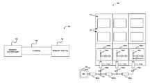
- FIG. 1Ashows a system 190 for providing electrical communication between a memory controller and a plurality of memory devices, in accordance with one embodiment.
- a memory controller 192is provided. Additionally, a plurality of memory devices 194 are provided. Still yet, a channel 196 is included for providing electrical communication between the memory controller 192 and the plurality of memory devices 196 , an impedance of the channel being at least partially controlled using High Density Interconnect (HDI) technology.
- HDIrefers to a technology utilized to condense integrated circuit packaging and printed circuit boards (PCBs) in order to obtain higher electrical performance, higher scale of integration, and more design convenience.
- a channelrefers to any component, connection, or group of components and/or connections, used to provide electrical communication between a memory device and a memory controller.
- the channel 196may include PCB transmission lines, module connectors, component packages, sockets, and/or any other components or connections that fit the above definition.
- the memory devices 194may include any type of memory device.
- the memory devices 194may include dynamic random access memory (DRAM).
- the memory controller 192may be any device capable of sending instructions or commands, or otherwise controlling the memory devices 194 .
- the channel 196may be connected to a plurality of DIMMs.
- at least one of the DIMMsmay include a micro-via.
- a micro-viarefers to a via constructed utilizing mico-via technology.
- a viarefers to any pad or strip with a plated hole that connects tracks from one layer of a substrate (e.g. a PCB) to another layer or layers.
- At least one of the DIMMsmay include a microstrip trace constructed on a board using HDI technology.
- a microstriprefers to any electrical transmission line on the surface layer of a PCB which can be used to convey electrical signals.
- the DIMMsmay include a read and/or write path.
- impedance controllingmay be utilized to adjust signal integrity properties of the read and/or write communication path.
- the impedance controllingmay use HDI technology.
- impedance controllingrefers to any altering or configuring of the impedance of a component.
- At least one interface circuitmay also be provided for allowing electrical communication between the memory controller 192 and at least one of the memory devices 194 , where the interface circuit may be utilized as an intermediate buffer or repeater chip between the memory controller 192 and at least one memory device 194 .
- the interface circuitmay be included as part of a DIMM.
- the interface circuitmay be electronically positioned between the memory controller 192 and at least one of the plurality of memory devices 194 . In this case, signals from the memory controller 192 to the memory devices 194 will pass though the interface circuit.
- the interface circuitmay include at least one programmable I/O driver.
- the programmable I/O drivermay be utilized to buffer the signals from memory controller 192 , recover the signal waveform quality, and resend them to at least one downstream memory device 194 .
- FIG. 1Bshows a system 100 for providing electrical communication between a host controller chip package 102 and one or more memory devices 118 .
- the electrical signalstraverse paths from the host controller chip package 102 through a socket 104 , traces 106 ( a )- 106 ( b ) on the surface of a printed circuit board (PCB) 107 , through a DIMM connector 108 , a resistor stub (Rstub) 110 ( a )- 110 ( c ), traces 112 ( a )- 112 ( b ) on the surface of the DIMMs 120 , any other interface connectors or circuits 114 , and finally to one or more memory devices 118 (e.g. DRAM, etc.).
- PCBprinted circuit board
- a plurality of DIMMs 120may be provided (e.g. DIMM# 1 -DIMM#N). Any number of DIMMs 120 may be included.
- the topology of the communication between the host controller chip package 102 and the memory devices 118is called a multi-drop topology.
- FIG. 1Cillustrates a system 150 corresponding to a schematic representation of the topology and interconnects for FIG. 1B .
- a memory controller 152which may be part of the host controller chip package 102 is connected to a buffer chip 154 ( a ) through traces (e.g. transmission lines) 106 ( a ) and 112 ( a ).
- the memory controller 152is connected to a buffer chip 154 ( b ) through traces 106 ( a ), 106 ( b ), and 112 ( b ).
- the memory controller 152is connected to a buffer chip 154 ( c ) through traces 106 ( a )- 106 ( c ), and 112 ( c ). Together, the traces form a channel such that the memory controller 152 may maintain electrical communication with the plurality of memory devices 118 .
- the system 150may include a motherboard (e.g. the PCB 107 ), multiple connectors, multiple resistor stubs, multiple DIMMs, multiple arrays of memory devices, and multiple interface circuits, etc. Further, each buffer chips 154 ( a )- 154 ( c ) may be situated electrically between the memory controller 152 and corresponding memory devices 118 , as shown.
- a motherboarde.g. the PCB 107
- each buffer chips 154 ( a )- 154 ( c )may be situated electrically between the memory controller 152 and corresponding memory devices 118 , as shown.
- the system 150may be constructed from components with various characteristics.
- the system 150may be constructed such that the traces 106 ( a )- 106 ( c ) may present an impedance (presented at point 157 ) of about 50 ohms to about 55 ohms.
- the impedance of the traces 106 ( a )- 106 ( c )may be 52.5 ohms.
- the resistive stubs 110 ( a )- 110 ( c )may be configured to have a resistance of about 8 ohms to about 12 ohms. In one exemplary embodiment, the resistive stubs 110 ( a )- 110 ( c ) may have a resistance of 10 ohms. Additionally, the DIMMs 120 may have an impedance of about 35 ohms to about 45 ohms at a point of the traces 112 ( a )- 112 ( c ). In one exemplary embodiment, the DIMMs 120 may have an impedance of 40 ohms.
- the on-die termination resistors 156 ( a )- 156 ( c )may be configured have a resistance of 20 Ohm, 20 Ohm, and off, respectively, if buffer chip 154 ( c ) is the active memory device in the operation.
- the resistive stubs 110 ( a )- 110 ( c )may be configured as 15 Ohm and the DIMMs 120 are configured as 68 Ohm.
- the resistive stubs 110 ( a )- 110 ( c )may be configured to have a resistance of about 20 ohms to about 24 ohms. In one exemplary embodiment, the resistive stubs 110 ( a )- 110 ( c ) may have a resistance of 22 ohms. In this case, the impedance of traces 112 ( a )- 112 ( c ) may be about 81 ohms to about 99 ohms. In one exemplary embodiment, the impedance of the traces 112 ( a )- 112 ( b ) may be 90 ohms.
- the on-die termination resistors (input bus termination, IBT) 156 ( a )- 156 ( c )may be configured have a resistance of 100 Ohm, 100 Ohm, 100 Ohm, respectively.
- the resistive stubs 110 ( a )- 110 ( c )are configured as 22 Ohm and the DIMMs 120 are configured as 68 Ohm.
- impedancesare specific examples, and should not be construed as limiting in any manner. Such impedances may vary depending on the particular implementation and components used.
- a PCB manufacturing technique known as High Density Interconnect (HDI), and Build-Up technologymay be employed.
- HDI technologyis a technique to condense integrated circuit packaging for increased microsystem density and high performance.
- HDI technologyis sometimes used as a generic term to denote a range of technologies that may be added to normal PCB technology to increase the density of interconnect.
- HDI packagingminimizes the size and weight of the electronics while maximizing performance.
- HDIallows three-dimensional wafer-scale packaging of integrated circuits.
- the particular features of HDI technology that are usedare the thin layers used as insulating material between conducting layers and micro-via holes that connect conducting layers and are drilled through the thin insulating layers.
- One way of constructing the thin insulating layersis using build-up technology, although other methods may equally be employed.
- One way of creating micro-viasis to use a laser to drill a precision hole through thin build-up layers, although other methods may equally be employed.
- the thin insulating layers and micro-vias provided by HDI technologyallow precise control over the transmission line impedance of the PCB interconnect as well as the unwanted parasitic impedances of the PCB interconnect.
- a micro-via manufacturing techniquemay be utilized to achieve the desired impedance at a point of the traces 112 ( a )- 112 ( c ).
- Micro-via technologyimplements a via between layers of a PCB wherein the via traverses only between the specific two layers of the PCB, resulting in elimination of redundant open via stubs with conventional through-hole vias, a much lower parasitic capacitance, a much smaller impedance discontinuity and accordingly a much lower amplitude of reflections.
- a viarefers to any pad or strip with a plated hole that connects tracks from one layer of a substrate (e.g. a PCB) to another layer or layers.
- flip-chipa PCB manufacturing technique known as flip-chip may be employed.
- Flip chip package technologyimplements signal connectivity between the package and a die that uses much less (and often a shortened run-length of) conductive material than other similarly purposed technologies employed for the stated connectivity such as wire bond, and therefore presents a much lower serial inductance, and accordingly a much lower impedance discontinuity and lower inductive crosstalk.
- a programmable I/O drivermay be employed.
- the drivermay be capable of presenting a range of drive strengths (e.g. drive strengths 1-N, where N is an integer).
- Each of the drive strength settingsnormally corresponds to a different value of effective or average driver resistance or impedance, though other factors such as shape, effective resistance, etc. of the drive curve at different voltage levels may also be varied.
- Such a strength valuemay be programmed using a variety of well known techniques, including setting the strength of the programmable buffer as a response to a command originating or sent through the memory controller 152 . Due to the nature of the multi-drop topology, the read path desires stronger driver strength than what memory devices on regular Register-DIMM can provide.
- Table 1shows specific memory cycles (namely, READ, WRITE, and CMD) illustrating the performance characteristics of a generic solution of the prior art, representative of commercial standards, versus an implementation of one embodiment discussed in the context of the present description. It should be noted that long valid data times (e.g. valid windows) supporting high frequency memory reads and writes are both highly valued, and elusive.
- Impedance Valid Impedance Valid Path Matching Window Matching WindowREAD ⁇ 70 ohm 300 ⁇ 40 ohm 700 driving picoseconds driving picoseconds into 40 into 40 ohm in ohm in parallel parallel with 40 with 40 ohm ohm WRITE ⁇ 40 ohms 280 ⁇ 40 ohm 580 driving picoseconds driving picoseconds into 80 in into 50 parallel ohm in with 40 parallel with 40 ohm CMD 630 1 picoseconds nanosecond
- impedance matching of the presently discussed embodimentsare nearly symmetric. This is in stark contrast to the extreme asymmetric nature of the prior art.
- impedance matchingrefers to configuring the impedances of different transmission line segments in a channel so that the impedance variation along the channel remains minimal.
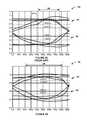
- FIGS. 2A and 2Bdepict eye diagrams 200 and 250 for a data READ cycle for double-data-rate three (DDR3) dual rank synchronous dynamic random access memory (SDRAM) at a speed of 1067 Mbps.
- FIG. 2Asubstantially illustrates the data shown for the generic READ memory cycle associated with the prior art. In particular, FIG. 2A shows a time that an eye is almost closed.
- DDR3double-data-rate three
- SDRAMsynchronous dynamic random access memory
- the valid window 206 of FIG. 2Ais only about 300 picoseconds, while the valid window 206 of an implementation of the presently discussed embodiments is about 700 picoseconds, as shown in FIG. 2B , which is more than twice as long as the prior art.
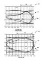
- FIGS. 3A and 3Bdepict eye diagrams 300 and 350 for a data WRITE cycle. Inspection of FIG. 3A illustrates data for the WRITE cycle associated with the prior art. More specifically, the time that high signals 302 are above the Vih(AC) voltage and the time that low signals 304 are below the Vil(DC) voltage defines a valid window 306 . As can be seen by inspection, the valid window of FIG. 3A is only about 350 picoseconds, while the valid window 306 of an implementation of the presently discussed embodiments is about 610 picoseconds, as shown in FIG. 3B .
- FIGS. 4A and 4Bdepict eye diagrams 400 and 450 for a CMD cycle. Inspection of FIG. 4A illustrates data for the CMD cycle associated with the prior art. More specifically a time that high signals 402 is above the Vih(AC) voltage and a time that low signals 404 are below the Vil(DC) voltage defines the valid window 406 . As can be seen by inspection, the valid window 406 of FIG. 4A is only about 700 picoseconds, while the valid window 406 of the presently discussed embodiments as shown in FIG. 4B is about 1.05 nanoseconds.
- FIGS. 5A and 5Bdepict a memory module (e.g. a DIMM) 500 and a corresponding buffer chip 502 which may be utilized in the context of the details of the FIGS. 1-4 .
- the memory module 500 and the buffer chip 502may be utilized in the context of the DIMMs 120 of FIGS. 1B and 1C .
- FIG. 6shows a system 600 including a system device 606 coupled to an interface circuit 602 and a plurality of memory circuits 604 A- 604 N, in accordance with one embodiment.
- the interface circuit 602is illustrated as an individual circuit, the interface circuit may also be represented by a plurality of interface circuits, each corresponding to one of the plurality of memory circuits 604 A- 604 N.
- the memory circuits 604 A- 604 Nmay be symmetrical, such that each has the same capacity, type, speed, etc. Of course, in other embodiments, the memory circuits 604 A- 604 N may be asymmetrical. For ease of illustration only, four such memory circuits 604 A- 604 N are shown, but actual embodiments may use any number of memory circuits. As will be discussed below, the memory chips may optionally be coupled to a memory module (not shown), such as a DIMM.
- the system device 606may be any type of system capable of requesting and/or initiating a process that results in an access of the memory circuits.
- the systemmay include a memory controller (not shown) through which it accesses the memory circuits 604 A- 604 N.
- the interface circuit 602may also include any circuit or logic capable of directly or indirectly communicating with the memory circuits, such as a memory controller, a buffer chip, advanced memory buffer (AMB) chip, etc.
- the interface circuit 602interfaces a plurality of signals 608 between the system device 606 and the memory circuits 604 A- 604 N.
- signals 608may include, for example, data signals, address signals, control signals, clock signals, and so forth.
- all of the signals communicated between the system device 606 and the memory circuits 604 A- 604 Nmay be communicated via the interface circuit 602 .
- some other signals 610are communicated directly between the system device 606 (or some component thereof, such as a memory controller, or a register, etc.) and the memory circuits 604 A- 604 N, without passing through the interface circuit 602 .
- the presence of a buffer chip between the memory controller and the plurality of memory circuits 604 A- 604 Nmay present a single smaller capacitive load on a channel as compared with multiple loads that would be presented by the plurality of memory devices in multiple rank DIMM systems, in absence of any buffer chip.
- an interface circuit 602may facilitate use of an input buffer design that has a lower input threshold requirement than normal memory chips. In other words, the interface circuit 602 is capable of receiving more noisy signals, or higher speed signals from the memory controller side than regular memory chips. Similarly, the presence of the interface circuit 602 may facilitate use of an output buffer design that is capable of not only driving with wider strength range, but also driving with wider range of edge rates, i.e., rise time. Faster edge rate may also facilitate the signal integrity of the data read path, given voltage margin is the main limiting factor. In addition, such an output buffer can be designed to operate more linearly than regular memory device output drivers.
- FIG. 7shows a DIMM 700 , in accordance with one embodiment.
- the DIMMincludes memory (e.g. DRAM) 702 , a repeater chip 704 (e.g. an interface circuit), a DIMM PCB 706 , a stub resister 708 , and a connector finger 710 .
- the repeater chip 704 , the DIMM PCB 706 , the stub resister 708 , and the connector finger 710may be configured, as described in the context of the details of the above embodiments, in order to provide a high-speed interface between the DRAM 702 and a memory controller (not shown).
- FIG. 8shows a graph 800 of a transfer function of a read function, in accordance with one embodiment.
- a transfer function 802 for the optimized memory channel designindicates significant improvement of channel bandwidth compared to a transfer function 804 of the original channel design on a wide range of frequencies.
- the graph 800represents an experiment with a DDR3, 3 DIMMs per channel topology, using a 1.4 volt power supply voltage on the stimulus source.
Landscapes
- Engineering & Computer Science (AREA)
- Theoretical Computer Science (AREA)
- General Engineering & Computer Science (AREA)
- Physics & Mathematics (AREA)
- General Physics & Mathematics (AREA)
- Computer Hardware Design (AREA)
- Dram (AREA)
- Semiconductor Memories (AREA)
- Memory System (AREA)
Abstract
Description
| TABLE 1 | ||
| Generic Embodiments | Presently Discussed Embodiments | |
| Impedance | Valid | Impedance | Valid | |
| Path | Matching | Window | Matching | Window |
| READ | ~70 | 300 | ~40 | 700 |
| driving | picoseconds | driving | picoseconds | |
| into 40 | into 40 | |||
| ohm in | ohm in | |||
| parallel | parallel | |||
| with 40 | with 40 | |||
| ohm | ohm | |||
| WRITE | ~40 ohms | 280 | ~40 ohm | 580 |
| driving | picoseconds | driving | picoseconds | |
| into 80 in | into 50 | |||
| parallel | ohm in | |||
| with 40 | parallel | |||
| with 40 | ||||
| ohm | ||||
| CMD | 630 | 1 | ||
| picoseconds | nanosecond | |||
Claims (20)
Priority Applications (4)
| Application Number | Priority Date | Filing Date | Title |
|---|---|---|---|
| US13/597,895US8675429B1 (en) | 2007-11-16 | 2012-08-29 | Optimal channel design for memory devices for providing a high-speed memory interface |
| US14/090,342US9171585B2 (en) | 2005-06-24 | 2013-11-26 | Configurable memory circuit system and method |
| US14/922,388US9507739B2 (en) | 2005-06-24 | 2015-10-26 | Configurable memory circuit system and method |
| US15/358,335US10013371B2 (en) | 2005-06-24 | 2016-11-22 | Configurable memory circuit system and method |
Applications Claiming Priority (3)
| Application Number | Priority Date | Filing Date | Title |
|---|---|---|---|
| US11/941,589US8111566B1 (en) | 2007-11-16 | 2007-11-16 | Optimal channel design for memory devices for providing a high-speed memory interface |
| US13/367,259US8279690B1 (en) | 2007-11-16 | 2012-02-06 | Optimal channel design for memory devices for providing a high-speed memory interface |
| US13/597,895US8675429B1 (en) | 2007-11-16 | 2012-08-29 | Optimal channel design for memory devices for providing a high-speed memory interface |
Related Parent Applications (1)
| Application Number | Title | Priority Date | Filing Date |
|---|---|---|---|
| US13/367,259ContinuationUS8279690B1 (en) | 2005-06-24 | 2012-02-06 | Optimal channel design for memory devices for providing a high-speed memory interface |
Related Child Applications (2)
| Application Number | Title | Priority Date | Filing Date |
|---|---|---|---|
| US11/611,374Continuation-In-PartUS8055833B2 (en) | 2005-06-24 | 2006-12-15 | System and method for increasing capacity, performance, and flexibility of flash storage |
| US14/090,342Continuation-In-PartUS9171585B2 (en) | 2005-06-24 | 2013-11-26 | Configurable memory circuit system and method |
Publications (1)
| Publication Number | Publication Date |
|---|---|
| US8675429B1true US8675429B1 (en) | 2014-03-18 |
Family
ID=45532256
Family Applications (3)
| Application Number | Title | Priority Date | Filing Date |
|---|---|---|---|
| US11/941,589Active2028-05-20US8111566B1 (en) | 2005-06-24 | 2007-11-16 | Optimal channel design for memory devices for providing a high-speed memory interface |
| US13/367,259ActiveUS8279690B1 (en) | 2005-06-24 | 2012-02-06 | Optimal channel design for memory devices for providing a high-speed memory interface |
| US13/597,895ActiveUS8675429B1 (en) | 2005-06-24 | 2012-08-29 | Optimal channel design for memory devices for providing a high-speed memory interface |
Family Applications Before (2)
| Application Number | Title | Priority Date | Filing Date |
|---|---|---|---|
| US11/941,589Active2028-05-20US8111566B1 (en) | 2005-06-24 | 2007-11-16 | Optimal channel design for memory devices for providing a high-speed memory interface |
| US13/367,259ActiveUS8279690B1 (en) | 2005-06-24 | 2012-02-06 | Optimal channel design for memory devices for providing a high-speed memory interface |
Country Status (1)
| Country | Link |
|---|---|
| US (3) | US8111566B1 (en) |
Cited By (6)
| Publication number | Priority date | Publication date | Assignee | Title |
|---|---|---|---|---|
| US8930647B1 (en) | 2011-04-06 | 2015-01-06 | P4tents1, LLC | Multiple class memory systems |
| US9158546B1 (en) | 2011-04-06 | 2015-10-13 | P4tents1, LLC | Computer program product for fetching from a first physical memory between an execution of a plurality of threads associated with a second physical memory |
| US9164679B2 (en) | 2011-04-06 | 2015-10-20 | Patents1, Llc | System, method and computer program product for multi-thread operation involving first memory of a first memory class and second memory of a second memory class |
| US9170744B1 (en) | 2011-04-06 | 2015-10-27 | P4tents1, LLC | Computer program product for controlling a flash/DRAM/embedded DRAM-equipped system |
| US9176671B1 (en) | 2011-04-06 | 2015-11-03 | P4tents1, LLC | Fetching data between thread execution in a flash/DRAM/embedded DRAM-equipped system |
| US9417754B2 (en) | 2011-08-05 | 2016-08-16 | P4tents1, LLC | User interface system, method, and computer program product |
Families Citing this family (13)
| Publication number | Priority date | Publication date | Assignee | Title |
|---|---|---|---|---|
| US9171585B2 (en) | 2005-06-24 | 2015-10-27 | Google Inc. | Configurable memory circuit system and method |
| US10013371B2 (en) | 2005-06-24 | 2018-07-03 | Google Llc | Configurable memory circuit system and method |
| US9507739B2 (en) | 2005-06-24 | 2016-11-29 | Google Inc. | Configurable memory circuit system and method |
| US8111566B1 (en)* | 2007-11-16 | 2012-02-07 | Google, Inc. | Optimal channel design for memory devices for providing a high-speed memory interface |
| US8233304B2 (en)* | 2008-07-28 | 2012-07-31 | Inphi Corporation | High speed memory module |
| US9888283B2 (en) | 2013-03-13 | 2018-02-06 | Nagrastar Llc | Systems and methods for performing transport I/O |
| USD758372S1 (en)* | 2013-03-13 | 2016-06-07 | Nagrastar Llc | Smart card interface |
| JP6200236B2 (en) | 2013-08-09 | 2017-09-20 | ルネサスエレクトロニクス株式会社 | Electronic equipment |
| US9237670B2 (en) | 2014-02-26 | 2016-01-12 | Samsung Electronics Co., Ltd. | Socket interposer and computer system using the socket |
| US20160134036A1 (en)* | 2014-11-12 | 2016-05-12 | Intel Corporation | Signal integrity in mutli-junction topologies |
| USD864968S1 (en) | 2015-04-30 | 2019-10-29 | Echostar Technologies L.L.C. | Smart card interface |
| US10291192B1 (en)* | 2018-03-09 | 2019-05-14 | Xilinx, Inc. | Programmable buffering, bandwidth extension and pre-emphasis of a track-and-hold circuit using series inductance |
| KR102640968B1 (en)* | 2018-05-29 | 2024-02-27 | 삼성전자주식회사 | Printed circuit board, storage device, and storage device including printed circuit board |
Citations (685)
| Publication number | Priority date | Publication date | Assignee | Title |
|---|---|---|---|---|
| US3800292A (en) | 1972-10-05 | 1974-03-26 | Honeywell Inf Systems | Variable masking for segmented memory |
| US4069452A (en) | 1976-09-15 | 1978-01-17 | Dana Laboratories, Inc. | Apparatus for automatically detecting values of periodically time varying signals |
| US4323965A (en) | 1980-01-08 | 1982-04-06 | Honeywell Information Systems Inc. | Sequential chip select decode apparatus and method |
| US4334307A (en) | 1979-12-28 | 1982-06-08 | Honeywell Information Systems Inc. | Data processing system with self testing and configuration mapping capability |
| US4345319A (en) | 1978-06-28 | 1982-08-17 | Cselt-Centro Studi E Laboratori Telecomunicazioni S.P.A. | Self-correcting, solid-state-mass-memory organized by bits and with reconfiguration capability for a stored program control system |
| US4392212A (en) | 1979-11-12 | 1983-07-05 | Fujitsu Limited | Semiconductor memory device with decoder for chip selection/write in |
| US4500958A (en) | 1982-04-21 | 1985-02-19 | Digital Equipment Corporation | Memory controller with data rotation arrangement |
| US4525921A (en) | 1981-07-13 | 1985-07-02 | Irvine Sensors Corporation | High-density electronic processing package-structure and fabrication |
| US4566082A (en) | 1983-03-23 | 1986-01-21 | Tektronix, Inc. | Memory pack addressing system |
| US4592019A (en) | 1983-08-31 | 1986-05-27 | At&T Bell Laboratories | Bus oriented LIFO/FIFO memory |
| US4646128A (en) | 1980-09-16 | 1987-02-24 | Irvine Sensors Corporation | High-density electronic processing package--structure and fabrication |
| US4698748A (en) | 1983-10-07 | 1987-10-06 | Essex Group, Inc. | Power-conserving control system for turning-off the power and the clocking for data transactions upon certain system inactivity |
| US4706166A (en) | 1986-04-25 | 1987-11-10 | Irvine Sensors Corporation | High-density electronic modules--process and product |
| US4710903A (en) | 1986-03-31 | 1987-12-01 | Wang Laboratories, Inc. | Pseudo-static memory subsystem |
| US4764846A (en) | 1987-01-05 | 1988-08-16 | Irvine Sensors Corporation | High density electronic package comprising stacked sub-modules |
| US4780843A (en) | 1983-11-07 | 1988-10-25 | Motorola, Inc. | Wait mode power reduction system and method for data processor |
| US4794597A (en) | 1986-03-28 | 1988-12-27 | Mitsubishi Denki Kabushiki Kaisha | Memory device equipped with a RAS circuit |
| US4796232A (en) | 1987-10-20 | 1989-01-03 | Contel Corporation | Dual port memory controller |
| US4807191A (en) | 1988-01-04 | 1989-02-21 | Motorola, Inc. | Redundancy for a block-architecture memory |
| US4841440A (en) | 1983-04-26 | 1989-06-20 | Nec Corporation | Control processor for controlling a peripheral unit |
| US4862347A (en) | 1986-04-22 | 1989-08-29 | International Business Machine Corporation | System for simulating memory arrays in a logic simulation machine |
| US4884237A (en) | 1984-03-28 | 1989-11-28 | International Business Machines Corporation | Stacked double density memory module using industry standard memory chips |
| US4887240A (en) | 1987-12-15 | 1989-12-12 | National Semiconductor Corporation | Staggered refresh for dram array |
| US4888687A (en) | 1987-05-04 | 1989-12-19 | Prime Computer, Inc. | Memory control system |
| US4899107A (en) | 1988-09-30 | 1990-02-06 | Micron Technology, Inc. | Discrete die burn-in for nonpackaged die |
| US4912678A (en) | 1987-09-26 | 1990-03-27 | Mitsubishi Denki Kabushiki Kaisha | Dynamic random access memory device with staggered refresh |
| US4922451A (en) | 1987-03-23 | 1990-05-01 | International Business Machines Corporation | Memory re-mapping in a microcomputer system |
| US4935734A (en) | 1985-09-11 | 1990-06-19 | Pilkington Micro-Electronics Limited | Semi-conductor integrated circuits/systems |
| US4937791A (en) | 1988-06-02 | 1990-06-26 | The California Institute Of Technology | High performance dynamic ram interface |
| US4956694A (en) | 1988-11-04 | 1990-09-11 | Dense-Pac Microsystems, Inc. | Integrated circuit chip stacking |
| US4982265A (en) | 1987-06-24 | 1991-01-01 | Hitachi, Ltd. | Semiconductor integrated circuit device and method of manufacturing the same |
| US4983533A (en) | 1987-10-28 | 1991-01-08 | Irvine Sensors Corporation | High-density electronic modules - process and product |
| US5025364A (en) | 1987-06-29 | 1991-06-18 | Hewlett-Packard Company | Microprocessor emulation system with memory mapping using variable definition and addressing of memory space |
| US5072424A (en) | 1985-07-12 | 1991-12-10 | Anamartic Limited | Wafer-scale integrated circuit memory |
| US5083266A (en) | 1986-12-26 | 1992-01-21 | Kabushiki Kaisha Toshiba | Microcomputer which enters sleep mode for a predetermined period of time on response to an activity of an input/output device |
| US5104820A (en) | 1989-07-07 | 1992-04-14 | Irvine Sensors Corporation | Method of fabricating electronic circuitry unit containing stacked IC layers having lead rerouting |
| US5193072A (en) | 1990-12-21 | 1993-03-09 | Vlsi Technology, Inc. | Hidden refresh of a dynamic random access memory |
| US5212666A (en) | 1989-07-10 | 1993-05-18 | Seiko Epson Corporation | Memory apparatus having flexibly designed memory capacity |
| US5220672A (en) | 1990-12-25 | 1993-06-15 | Mitsubishi Denki Kabushiki Kaisha | Low power consuming digital circuit device |
| US5222014A (en) | 1992-03-02 | 1993-06-22 | Motorola, Inc. | Three-dimensional multi-chip pad array carrier |
| US5241266A (en) | 1992-04-10 | 1993-08-31 | Micron Technology, Inc. | Built-in test circuit connection for wafer level burnin and testing of individual dies |
| US5252807A (en) | 1990-07-02 | 1993-10-12 | George Chizinsky | Heated plate rapid thermal processor |
| US5257233A (en) | 1990-10-31 | 1993-10-26 | Micron Technology, Inc. | Low power memory module using restricted RAM activation |
| US5278796A (en) | 1991-04-12 | 1994-01-11 | Micron Technology, Inc. | Temperature-dependent DRAM refresh circuit |
| US5282177A (en) | 1992-04-08 | 1994-01-25 | Micron Technology, Inc. | Multiple register block write method and circuit for video DRAMs |
| US5332922A (en) | 1990-04-26 | 1994-07-26 | Hitachi, Ltd. | Multi-chip semiconductor package |
| US5347428A (en) | 1992-12-03 | 1994-09-13 | Irvine Sensors Corporation | Module comprising IC memory stack dedicated to and structurally combined with an IC microprocessor chip |
| US5369749A (en) | 1989-05-17 | 1994-11-29 | Ibm Corporation | Method and apparatus for the direct transfer of information between application programs running on distinct processors without utilizing the services of one or both operating systems |
| US5384745A (en) | 1992-04-27 | 1995-01-24 | Mitsubishi Denki Kabushiki Kaisha | Synchronous semiconductor memory device |
| US5388265A (en) | 1992-03-06 | 1995-02-07 | Intel Corporation | Method and apparatus for placing an integrated circuit chip in a reduced power consumption state |
| US5390334A (en) | 1990-10-29 | 1995-02-14 | International Business Machines Corporation | Workstation power management by page placement control |
| US5392251A (en) | 1993-07-13 | 1995-02-21 | Micron Semiconductor, Inc. | Controlling dynamic memory refresh cycle time |
| EP0644547A2 (en) | 1993-09-13 | 1995-03-22 | International Business Machines Corporation | Integrated multichip memory module, structure and fabrication |
| US5408190A (en) | 1991-06-04 | 1995-04-18 | Micron Technology, Inc. | Testing apparatus having substrate interconnect for discrete die burn-in for nonpackaged die |
| US5432729A (en) | 1993-04-23 | 1995-07-11 | Irvine Sensors Corporation | Electronic module comprising a stack of IC chips each interacting with an IC chip secured to the stack |
| US5448511A (en) | 1994-06-01 | 1995-09-05 | Storage Technology Corporation | Memory stack with an integrated interconnect and mounting structure |
| US5453434A (en) | 1989-11-13 | 1995-09-26 | Allergan, Inc. | N-substituted derivatives of 3R,4R-ethyl-[(1-methyl-1H-imidazol-5-yl)methyl]-2-pyrrolidone |
| US5467455A (en) | 1993-11-03 | 1995-11-14 | Motorola, Inc. | Data processing system and method for performing dynamic bus termination |
| US5483497A (en) | 1993-08-24 | 1996-01-09 | Fujitsu Limited | Semiconductor memory having a plurality of banks usable in a plurality of bank configurations |
| US5498886A (en) | 1991-11-05 | 1996-03-12 | Monolithic System Technology, Inc. | Circuit module redundancy architecture |
| US5502333A (en) | 1994-03-30 | 1996-03-26 | International Business Machines Corporation | Semiconductor stack structures and fabrication/sparing methods utilizing programmable spare circuit |
| US5513339A (en) | 1992-09-30 | 1996-04-30 | At&T Corp. | Concurrent fault simulation of circuits with both logic elements and functional circuits |
| US5513135A (en) | 1994-12-02 | 1996-04-30 | International Business Machines Corporation | Synchronous memory packaged in single/dual in-line memory module and method of fabrication |
| US5519832A (en) | 1992-11-13 | 1996-05-21 | Digital Equipment Corporation | Method and apparatus for displaying module diagnostic results |
| US5526320A (en) | 1994-12-23 | 1996-06-11 | Micron Technology Inc. | Burst EDO memory device |
| US5530836A (en) | 1994-08-12 | 1996-06-25 | International Business Machines Corporation | Method and apparatus for multiple memory bank selection |
| US5550781A (en) | 1989-05-08 | 1996-08-27 | Hitachi Maxell, Ltd. | Semiconductor apparatus with two activating modes of different number of selected word lines at refreshing |
| US5559990A (en) | 1992-02-14 | 1996-09-24 | Advanced Micro Devices, Inc. | Memories with burst mode access |
| US5561622A (en) | 1993-09-13 | 1996-10-01 | International Business Machines Corporation | Integrated memory cube structure |
| US5566344A (en) | 1994-12-20 | 1996-10-15 | National Semiconductor Corporation | In-system programming architecture for a multiple chip processor |
| US5581498A (en) | 1993-08-13 | 1996-12-03 | Irvine Sensors Corporation | Stack of IC chips in lieu of single IC chip |
| US5590071A (en) | 1995-11-16 | 1996-12-31 | International Business Machines Corporation | Method and apparatus for emulating a high capacity DRAM |
| US5598376A (en) | 1994-12-23 | 1997-01-28 | Micron Technology, Inc. | Distributed write data drivers for burst access memories |
| US5604714A (en) | 1995-11-30 | 1997-02-18 | Micron Technology, Inc. | DRAM having multiple column address strobe operation |
| US5608262A (en) | 1995-02-24 | 1997-03-04 | Lucent Technologies Inc. | Packaging multi-chip modules without wire-bond interconnection |
| US5610864A (en) | 1994-12-23 | 1997-03-11 | Micron Technology, Inc. | Burst EDO memory device with maximized write cycle timing |
| US5627791A (en) | 1996-02-16 | 1997-05-06 | Micron Technology, Inc. | Multiple bank memory with auto refresh to specified bank |
| US5640364A (en) | 1994-12-23 | 1997-06-17 | Micron Technology, Inc. | Self-enabling pulse trapping circuit |
| US5640337A (en) | 1992-07-10 | 1997-06-17 | Lsi Logic Corp. | Method and apparatus for interim in-situ testing of an electronic system with an inchoate ASIC |
| US5652724A (en) | 1994-12-23 | 1997-07-29 | Micron Technology, Inc. | Burst EDO memory device having pipelined output buffer |
| US5654204A (en) | 1994-07-20 | 1997-08-05 | Anderson; James C. | Die sorter |
| US5661677A (en) | 1996-05-15 | 1997-08-26 | Micron Electronics, Inc. | Circuit and method for on-board programming of PRD Serial EEPROMS |
| US5668773A (en) | 1994-12-23 | 1997-09-16 | Micron Technology, Inc. | Synchronous burst extended data out DRAM |
| US5675549A (en) | 1994-12-23 | 1997-10-07 | Micron Technology, Inc. | Burst EDO memory device address counter |
| US5680342A (en) | 1996-04-10 | 1997-10-21 | International Business Machines Corporation | Memory module package with address bus buffering |
| US5682354A (en) | 1995-11-06 | 1997-10-28 | Micron Technology, Inc. | CAS recognition in burst extended data out DRAM |
| US5692121A (en) | 1995-04-14 | 1997-11-25 | International Business Machines Corporation | Recovery unit for mirrored processors |
| US5692202A (en) | 1995-12-29 | 1997-11-25 | Intel Corporation | System, apparatus, and method for managing power in a computer system |
| US5696929A (en) | 1995-10-03 | 1997-12-09 | Intel Corporation | Flash EEPROM main memory in a computer system |
| US5717654A (en) | 1995-02-10 | 1998-02-10 | Micron Technology, Inc. | Burst EDO memory device with maximized write cycle timing |
| USRE35733E (en) | 1991-11-26 | 1998-02-17 | Circuit Components Incorporated | Device for interconnecting integrated circuit packages to circuit boards |
| US5721859A (en) | 1994-12-23 | 1998-02-24 | Micron Technology, Inc. | Counter control circuit in a burst memory |
| US5724288A (en) | 1995-08-30 | 1998-03-03 | Micron Technology, Inc. | Data communication for memory |
| US5729503A (en) | 1994-12-23 | 1998-03-17 | Micron Technology, Inc. | Address transition detection on a synchronous design |
| US5729504A (en) | 1995-12-14 | 1998-03-17 | Micron Technology, Inc. | Continuous burst edo memory device |
| US5742792A (en) | 1993-04-23 | 1998-04-21 | Emc Corporation | Remote data mirroring |
| US5748914A (en) | 1995-10-19 | 1998-05-05 | Rambus, Inc. | Protocol for communication with dynamic memory |
| US5752045A (en) | 1995-07-14 | 1998-05-12 | United Microelectronics Corporation | Power conservation in synchronous SRAM cache memory blocks of a computer system |
| US5761703A (en) | 1996-08-16 | 1998-06-02 | Unisys Corporation | Apparatus and method for dynamic memory refresh |
| US5760478A (en) | 1996-08-20 | 1998-06-02 | International Business Machines Corporation | Clock skew minimization system and method for integrated circuits |
| US5781766A (en) | 1996-05-13 | 1998-07-14 | National Semiconductor Corporation | Programmable compensating device to optimize performance in a DRAM controller chipset |
| US5787457A (en) | 1996-10-18 | 1998-07-28 | International Business Machines Corporation | Cached synchronous DRAM architecture allowing concurrent DRAM operations |
| US5798961A (en) | 1994-08-23 | 1998-08-25 | Emc Corporation | Non-volatile memory module |
| US5802555A (en) | 1995-03-15 | 1998-09-01 | Texas Instruments Incorporated | Computer system including a refresh controller circuit having a row address strobe multiplexer and associated method |
| US5802395A (en) | 1996-07-08 | 1998-09-01 | International Business Machines Corporation | High density memory modules with improved data bus performance |
| US5819065A (en) | 1995-06-28 | 1998-10-06 | Quickturn Design Systems, Inc. | System and method for emulating memory |
| US5818788A (en) | 1997-05-30 | 1998-10-06 | Nec Corporation | Circuit technique for logic integrated DRAM with SIMD architecture and a method for controlling low-power, high-speed and highly reliable operation |
| US5831833A (en) | 1995-07-17 | 1998-11-03 | Nec Corporation | Bear chip mounting printed circuit board and a method of manufacturing thereof by photoetching |
| US5835435A (en) | 1997-12-02 | 1998-11-10 | Intel Corporation | Method and apparatus for dynamically placing portions of a memory in a reduced power consumtion state |
| US5838177A (en) | 1997-01-06 | 1998-11-17 | Micron Technology, Inc. | Adjustable output driver circuit having parallel pull-up and pull-down elements |
| US5838165A (en) | 1996-08-21 | 1998-11-17 | Chatter; Mukesh | High performance self modifying on-the-fly alterable logic FPGA, architecture and method |
| US5841580A (en) | 1990-04-18 | 1998-11-24 | Rambus, Inc. | Integrated circuit I/O using a high performance bus interface |
| US5845108A (en) | 1995-12-22 | 1998-12-01 | Samsung Electronics, Co., Ltd. | Semiconductor memory device using asynchronous signal |
| US5843807A (en) | 1993-03-29 | 1998-12-01 | Staktek Corporation | Method of manufacturing an ultra-high density warp-resistant memory module |
| US5850368A (en) | 1995-06-01 | 1998-12-15 | Micron Technology, Inc. | Burst EDO memory address counter |
| US5860106A (en) | 1995-07-13 | 1999-01-12 | Intel Corporation | Method and apparatus for dynamically adjusting power/performance characteristics of a memory subsystem |
| US5870350A (en) | 1997-05-21 | 1999-02-09 | International Business Machines Corporation | High performance, high bandwidth memory bus architecture utilizing SDRAMs |
| US5870347A (en) | 1997-03-11 | 1999-02-09 | Micron Technology, Inc. | Multi-bank memory input/output line selection |
| US5872907A (en) | 1991-12-16 | 1999-02-16 | International Business Machines Corporation | Fault tolerant design for identification of AC defects including variance of cycle time to maintain system operation |
| US5875142A (en) | 1997-06-17 | 1999-02-23 | Micron Technology, Inc. | Integrated circuit with temperature detector |
| US5878279A (en) | 1995-08-03 | 1999-03-02 | Sgs-Thomson Microelectronics S.A. | HDLC integrated circuit using internal arbitration to prioritize access to a shared internal bus amongst a plurality of devices |
| US5901105A (en) | 1995-04-05 | 1999-05-04 | Ong; Adrian E | Dynamic random access memory having decoding circuitry for partial memory blocks |
| US5903500A (en) | 1997-04-11 | 1999-05-11 | Intel Corporation | 1.8 volt output buffer on flash memories |
| US5905688A (en) | 1997-04-01 | 1999-05-18 | Lg Semicon Co., Ltd. | Auto power down circuit for a semiconductor memory device |
| US5907512A (en) | 1989-08-14 | 1999-05-25 | Micron Technology, Inc. | Mask write enablement for memory devices which permits selective masked enablement of plural segments |
| US5910010A (en) | 1994-04-26 | 1999-06-08 | Hitachi, Ltd. | Semiconductor integrated circuit device, and process and apparatus for manufacturing the same |
| US5913072A (en) | 1997-04-08 | 1999-06-15 | Wieringa; Fred | Image processing system in which image processing programs stored in a personal computer are selectively executed through user interface of a scanner |
| US5915167A (en) | 1997-04-04 | 1999-06-22 | Elm Technology Corporation | Three dimensional structure memory |
| US5917758A (en) | 1996-11-04 | 1999-06-29 | Micron Technology, Inc. | Adjustable output driver circuit |
| US5924111A (en) | 1995-10-17 | 1999-07-13 | Huang; Chu-Kai | Method and system for interleaving data in multiple memory bank partitions |
| US5923611A (en) | 1996-12-20 | 1999-07-13 | Micron Technology, Inc. | Memory having a plurality of external clock signal inputs |
| US5926435A (en) | 1996-12-31 | 1999-07-20 | Hyundai Electronics Industries Co., Ltd. | Apparatus for saving power consumption in semiconductor memory devices |
| US5929650A (en) | 1997-02-04 | 1999-07-27 | Motorola, Inc. | Method and apparatus for performing operative testing on an integrated circuit |
| US5943254A (en) | 1995-02-22 | 1999-08-24 | International Business Machines Corporation | Multichip semiconductor structures with consolidated circuitry and programmable ESD protection for input/output nodes |
| US5949254A (en) | 1996-11-26 | 1999-09-07 | Micron Technology, Inc. | Adjustable output driver circuit |
| US5953263A (en) | 1997-02-10 | 1999-09-14 | Rambus Inc. | Synchronous memory device having a programmable register and method of controlling same |
| US5953215A (en) | 1997-12-01 | 1999-09-14 | Karabatsos; Chris | Apparatus and method for improving computer memory speed and capacity |
| US5956233A (en) | 1997-12-19 | 1999-09-21 | Texas Instruments Incorporated | High density single inline memory module |
| US5963429A (en) | 1997-08-20 | 1999-10-05 | Sulzer Intermedics Inc. | Printed circuit substrate with cavities for encapsulating integrated circuits |
| US5962435A (en) | 1993-12-10 | 1999-10-05 | Hoechst Marion Roussel, Inc. | Method of lowering serum cholesterol levels with 2,6-di-alkyl-4-silyl-phenols |
| US5963464A (en) | 1998-02-26 | 1999-10-05 | International Business Machines Corporation | Stackable memory card |
| US5966724A (en) | 1996-01-11 | 1999-10-12 | Micron Technology, Inc. | Synchronous memory device with dual page and burst mode operations |
| US5966727A (en) | 1996-07-12 | 1999-10-12 | Dux Inc. | Combination flash memory and dram memory board interleave-bypass memory access method, and memory access device incorporating both the same |
| US5969996A (en) | 1995-04-25 | 1999-10-19 | Hiachi, Ltd. | Semiconductor memory device and memory system |
| US5973392A (en) | 1997-04-02 | 1999-10-26 | Nec Corporation | Stacked carrier three-dimensional memory module and semiconductor device using the same |
| US5978304A (en) | 1998-06-30 | 1999-11-02 | Lsi Logic Corporation | Hierarchical, adaptable-configuration dynamic random access memory |
| US5995443A (en) | 1990-04-18 | 1999-11-30 | Rambus Inc. | Synchronous memory device |
| US5995424A (en) | 1997-07-16 | 1999-11-30 | Tanisys Technology, Inc. | Synchronous memory test system |
| US6001671A (en) | 1996-04-18 | 1999-12-14 | Tessera, Inc. | Methods for manufacturing a semiconductor package having a sacrificial layer |
| US6014339A (en) | 1997-04-03 | 2000-01-11 | Fujitsu Limited | Synchronous DRAM whose power consumption is minimized |
| US6016282A (en) | 1998-05-28 | 2000-01-18 | Micron Technology, Inc. | Clock vernier adjustment |
| US6026050A (en) | 1997-07-09 | 2000-02-15 | Micron Technology, Inc. | Method and apparatus for adaptively adjusting the timing of a clock signal used to latch digital signals, and memory device using same |
| US6026027A (en) | 1994-01-31 | 2000-02-15 | Norand Corporation | Flash memory system having memory cache |
| US6029250A (en) | 1998-09-09 | 2000-02-22 | Micron Technology, Inc. | Method and apparatus for adaptively adjusting the timing offset between a clock signal and digital signals transmitted coincident with that clock signal, and memory device and system using same |
| US6034916A (en) | 1997-11-18 | 2000-03-07 | Samsung Electronics Co., Ltd. | Data masking circuits and methods for integrated circuit memory devices, including data strobe signal synchronization |
| US6038673A (en) | 1998-11-03 | 2000-03-14 | Intel Corporation | Computer system with power management scheme for DRAM devices |
| US6044032A (en) | 1998-12-03 | 2000-03-28 | Micron Technology, Inc. | Addressing scheme for a double data rate SDRAM |
| US6047361A (en) | 1996-08-21 | 2000-04-04 | International Business Machines Corporation | Memory control device, with a common synchronous interface coupled thereto, for accessing asynchronous memory devices and different synchronous devices |
| US6047344A (en) | 1997-03-05 | 2000-04-04 | Kabushiki Kaisha Toshiba | Semiconductor memory device with multiplied internal clock |
| US6047073A (en) | 1994-11-02 | 2000-04-04 | Advanced Micro Devices, Inc. | Digital wavetable audio synthesizer with delay-based effects processing |
| US6053948A (en) | 1995-06-07 | 2000-04-25 | Synopsys, Inc. | Method and apparatus using a memory model |
| US6058451A (en) | 1997-12-22 | 2000-05-02 | Emc Corporation | Method and apparatus for refreshing a non-clocked memory |
| US6065092A (en) | 1994-11-30 | 2000-05-16 | Hitachi Micro Systems, Inc. | Independent and cooperative multichannel memory architecture for use with master device |
| US6073223A (en) | 1997-07-21 | 2000-06-06 | Hewlett-Packard Company | Memory controller and method for intermittently activating and idling a clock signal for a synchronous memory |
| US6075730A (en) | 1997-10-10 | 2000-06-13 | Rambus Incorporated | High performance cost optimized memory with delayed memory writes |
| US6075744A (en) | 1997-10-10 | 2000-06-13 | Rambus Inc. | Dram core refresh with reduced spike current |
| US6079025A (en) | 1990-06-01 | 2000-06-20 | Vadem | System and method of computer operating mode control for power consumption reduction |
| US6078546A (en) | 1997-03-18 | 2000-06-20 | Samsung Electronics Co., Ltd. | Synchronous semiconductor memory device with double data rate scheme |
| US6088290A (en) | 1997-08-13 | 2000-07-11 | Kabushiki Kaisha Toshiba | Semiconductor memory device having a power-down mode |
| US6091251A (en) | 1991-06-04 | 2000-07-18 | Wood; Alan G. | Discrete die burn-in for nonpackaged die |
| US6101564A (en) | 1995-08-03 | 2000-08-08 | Sgs-Thomson Microelectronics S.A. | Device for organizing the access to a memory bus |
| US6108795A (en) | 1998-10-30 | 2000-08-22 | Micron Technology, Inc. | Method for aligning clock and data signals received from a RAM |
| USRE36839E (en) | 1995-02-14 | 2000-08-29 | Philips Semiconductor, Inc. | Method and apparatus for reducing power consumption in digital electronic circuits |
| US6111812A (en) | 1999-07-23 | 2000-08-29 | Micron Technology, Inc. | Method and apparatus for adjusting control signal timing in a memory device |
| US6125072A (en) | 1998-07-21 | 2000-09-26 | Seagate Technology, Inc. | Method and apparatus for contiguously addressing a memory system having vertically expanded multiple memory arrays |
| US6134638A (en) | 1997-08-13 | 2000-10-17 | Compaq Computer Corporation | Memory controller supporting DRAM circuits with different operating speeds |
| US6154370A (en) | 1998-07-21 | 2000-11-28 | Lucent Technologies Inc. | Recessed flip-chip package |
| US6166991A (en) | 1999-11-03 | 2000-12-26 | Cypress Semiconductor Corp. | Circuit, architecture and method for reducing power consumption in a synchronous integrated circuit |
| US6181640B1 (en) | 1997-06-24 | 2001-01-30 | Hyundai Electronics Industries Co., Ltd. | Control circuit for semiconductor memory device |
| US6199151B1 (en) | 1998-06-05 | 2001-03-06 | Intel Corporation | Apparatus and method for storing a device row indicator for use in a subsequent page-miss memory cycle |
| US6208168B1 (en) | 1997-06-27 | 2001-03-27 | Samsung Electronics Co., Ltd. | Output driver circuits having programmable pull-up and pull-down capability for driving variable loads |
| US6216246B1 (en) | 1996-05-24 | 2001-04-10 | Jeng-Jye Shau | Methods to make DRAM fully compatible with SRAM using error correction code (ECC) mechanism |
| US6222739B1 (en) | 1998-01-20 | 2001-04-24 | Viking Components | High-density computer module with stacked parallel-plane packaging |
| US6226730B1 (en) | 1998-06-05 | 2001-05-01 | Intel Corporation | Achieving page hit memory cycles on a virtual address reference |
| US6226709B1 (en) | 1997-10-24 | 2001-05-01 | Compaq Computer Corporation | Memory refresh control system |
| US20010000822A1 (en) | 1998-04-28 | 2001-05-03 | Dell Timothy Jay | Dynamic configuration of memory module using presence detect data |
| US6233650B1 (en) | 1998-04-01 | 2001-05-15 | Intel Corporation | Using FET switches for large memory arrays |
| US6233192B1 (en) | 1998-03-05 | 2001-05-15 | Sharp Kabushiki Kaisha | Semiconductor memory device |
| US6240048B1 (en) | 1999-06-29 | 2001-05-29 | Nec Corporation | Synchronous type semiconductor memory system with less power consumption |
| US20010003198A1 (en) | 1999-11-30 | 2001-06-07 | Chung-Che Wu | Method for timing setting of a system memory |
| US6252807B1 (en) | 1999-08-06 | 2001-06-26 | Mitsubishi Electric Engineering Company, Limited | Memory device with reduced power consumption when byte-unit accessed |
| US6253278B1 (en) | 1996-08-15 | 2001-06-26 | Micron Technology, Inc. | Synchronous DRAM modules including multiple clock out signals for increasing processing speed |
| US6260154B1 (en) | 1998-10-30 | 2001-07-10 | Micron Technology, Inc. | Apparatus for aligning clock and data signals received from a RAM |
| US6262938B1 (en) | 1999-03-03 | 2001-07-17 | Samsung Electronics Co., Ltd. | Synchronous DRAM having posted CAS latency and method for controlling CAS latency |
| US20010011322A1 (en) | 1998-06-22 | 2001-08-02 | Patrick F. Stolt | Data strobe for faster data access from a memory array |
| US6274395B1 (en) | 1999-12-23 | 2001-08-14 | Lsi Logic Corporation | Method and apparatus for maintaining test data during fabrication of a semiconductor wafer |
| US6279069B1 (en) | 1996-12-26 | 2001-08-21 | Intel Corporation | Interface for flash EEPROM memory arrays |
| US20010019509A1 (en) | 1999-12-22 | 2001-09-06 | Ari Aho | Memory controller |
| US20010021106A1 (en) | 1999-01-14 | 2001-09-13 | Rick Weber | Stacked printed circuit board memory module |
| US20010021137A1 (en) | 2000-03-13 | 2001-09-13 | Yasukazu Kai | Dynamic random access memory |
| US6295572B1 (en) | 1994-01-24 | 2001-09-25 | Advanced Micro Devices, Inc. | Integrated SCSI and ethernet controller on a PCI local bus |
| US6298426B1 (en) | 1997-12-31 | 2001-10-02 | Intel Corporation | Controller configurable for use with multiple memory organizations |
| US6307769B1 (en) | 1999-09-02 | 2001-10-23 | Micron Technology, Inc. | Semiconductor devices having mirrored terminal arrangements, devices including same, and methods of testing such semiconductor devices |
| US6317381B1 (en) | 1999-12-07 | 2001-11-13 | Micron Technology, Inc. | Method and system for adaptively adjusting control signal timing in a memory device |
| US6317352B1 (en) | 2000-09-18 | 2001-11-13 | Intel Corporation | Apparatus for implementing a buffered daisy chain connection between a memory controller and memory modules |
| US6324120B2 (en) | 1990-04-18 | 2001-11-27 | Rambus Inc. | Memory device having a variable data output length |
| US20010046163A1 (en) | 2000-05-19 | 2001-11-29 | Fujitsu Limited | Memory system and memory controller with reliable data latch operation |
| US20010046129A1 (en) | 2000-05-24 | 2001-11-29 | International Business Machines Corporation | Interposer for connecting two substrates and resulting assembly |
| US6327664B1 (en) | 1999-04-30 | 2001-12-04 | International Business Machines Corporation | Power management on a memory card having a signal processing element |
| US20010052062A1 (en) | 1994-03-01 | 2001-12-13 | G. Jack Lipovski | Parallel computer within dynamic random access memory |
| US6336174B1 (en) | 1999-08-09 | 2002-01-01 | Maxtor Corporation | Hardware assisted memory backup system and method |
| US20020002662A1 (en) | 1998-07-13 | 2002-01-03 | Olarig Sompong Paul | Method and apparatus for supporting heterogeneous memory in computer systems |
| US6338113B1 (en) | 1998-06-10 | 2002-01-08 | Mitsubishi Denki Kabushiki Kaisha | Memory module system having multiple memory modules |
| US6338108B1 (en) | 1997-04-15 | 2002-01-08 | Nec Corporation | Coprocessor-integrated packet-type memory LSI, packet-type memory/coprocessor bus, and control method thereof |
| US20020004897A1 (en) | 2000-07-05 | 2002-01-10 | Min-Cheng Kao | Data processing apparatus for executing multiple instruction sets |
| US6341347B1 (en) | 1999-05-11 | 2002-01-22 | Sun Microsystems, Inc. | Thread switch logic in a multiple-thread processor |
| JP2002025255A (en) | 2000-07-04 | 2002-01-25 | Hitachi Ltd | Semiconductor storage device |
| US6343019B1 (en) | 1997-12-22 | 2002-01-29 | Micron Technology, Inc. | Apparatus and method of stacking die on a substrate |
| US20020015340A1 (en) | 2000-07-03 | 2002-02-07 | Victor Batinovich | Method and apparatus for memory module circuit interconnection |
| US20020019961A1 (en) | 1998-08-28 | 2002-02-14 | Blodgett Greg A. | Device and method for repairing a semiconductor memory |
| US6353561B1 (en) | 1998-09-18 | 2002-03-05 | Fujitsu Limited | Semiconductor integrated circuit and method for controlling the same |
| US6356105B1 (en) | 2000-06-28 | 2002-03-12 | Intel Corporation | Impedance control system for a center tapped termination bus |
| US6356500B1 (en) | 2000-08-23 | 2002-03-12 | Micron Technology, Inc. | Reduced power DRAM device and method |
| US20020038405A1 (en) | 1998-09-30 | 2002-03-28 | Michael W. Leddige | Method and apparatus for implementing multiple memory buses on a memory module |
| US20020040416A1 (en) | 2000-07-19 | 2002-04-04 | Tsern Ely K. | Memory controller with power management logic |
| US20020041507A1 (en) | 2000-10-10 | 2002-04-11 | Woo Steven C. | Methods and systems for reducing heat flux in memory systems |
| US6381668B1 (en) | 1997-03-21 | 2002-04-30 | International Business Machines Corporation | Address mapping for system memory |
| US6381188B1 (en) | 1999-01-12 | 2002-04-30 | Samsung Electronics Co., Ltd. | DRAM capable of selectively performing self-refresh operation for memory bank |
| US20020051398A1 (en) | 2000-09-12 | 2002-05-02 | Seiko Epson Corporation | Semiconductor device, method for refreshing the same, system memory, and electronics apparatus |
| US6389514B1 (en) | 1999-03-25 | 2002-05-14 | Hewlett-Packard Company | Method and computer system for speculatively closing pages in memory |
| US6392304B1 (en) | 1998-11-12 | 2002-05-21 | United Memories, Inc. | Multi-chip memory apparatus and associated method |
| US20020060948A1 (en) | 2000-11-21 | 2002-05-23 | Nai-Shung Chang | Clock device for supporting multiplicity of memory module types |
| US20020060945A1 (en) | 2000-11-20 | 2002-05-23 | Fujitsu Limited | Synchronous semiconductor device and method for latching input signals |
| US20020064083A1 (en) | 2000-11-24 | 2002-05-30 | Ryu Dong-Ryul | Clock generating circuits controlling activation of a delay locked loop circuit on transition to a standby mode of a semiconductor memory device and methods for operating the same |
| US20020064073A1 (en) | 2000-11-30 | 2002-05-30 | Pien Chien | Dram module and method of using sram to replace damaged dram cell |
| US6414868B1 (en) | 1999-06-07 | 2002-07-02 | Sun Microsystems, Inc. | Memory expansion module including multiple memory banks and a bank control circuit |
| US20020089831A1 (en) | 2001-01-09 | 2002-07-11 | Forthun John A. | Module with one side stacked memory |
| US20020089970A1 (en) | 1998-01-08 | 2002-07-11 | Kabushiki Kaisha Toshiba | Multimedia private branch exchanger and private branch exchange system |
| US6421754B1 (en) | 1994-12-22 | 2002-07-16 | Texas Instruments Incorporated | System management mode circuits, systems and methods |
| US20020094671A1 (en) | 1996-03-07 | 2002-07-18 | Distefano Thomas H. | Methods for providing void-free layers for semiconductor assemblies |
| JP3304893B2 (en) | 1994-06-28 | 2002-07-22 | 日本電気株式会社 | Memory selection circuit and semiconductor memory device |
| US6424532B2 (en) | 1998-06-12 | 2002-07-23 | Nec Corporation | Heat sink and memory module with heat sink |
| US6430103B2 (en) | 2000-02-03 | 2002-08-06 | Hitachi, Ltd. | Semiconductor integrated circuit device with memory banks and read buffer capable of storing data read out from one memory bank when data of another memory bank is outputting |
| US6429029B1 (en) | 1997-01-15 | 2002-08-06 | Formfactor, Inc. | Concurrent design and subsequent partitioning of product and test die |
| US6434660B1 (en) | 2000-05-23 | 2002-08-13 | Centennial Technologies, Inc. | Emulating one tape protocol of flash memory to a different type protocol of flash memory |
| US6438057B1 (en) | 2001-07-06 | 2002-08-20 | Infineon Technologies Ag | DRAM refresh timing adjustment device, system and method |
| US6442698B2 (en) | 1998-11-04 | 2002-08-27 | Intel Corporation | Method and apparatus for power management in a memory subsystem |
| US6445591B1 (en) | 2000-08-10 | 2002-09-03 | Nortel Networks Limited | Multilayer circuit board |
| US20020121670A1 (en) | 2001-03-01 | 2002-09-05 | Matsushita Electric Industrial Co., Ltd. | Lead frame |
| US20020121650A1 (en) | 2001-03-01 | 2002-09-05 | Masanori Minamio | Resin-encapsulated semiconductor device and method for manufacturing the same |
| US20020129204A1 (en) | 2001-03-06 | 2002-09-12 | Lance Leighnor | Hypercache RAM based disk emulation and method |
| US6452826B1 (en) | 2000-10-26 | 2002-09-17 | Samsung Electronics Co., Ltd. | Memory module system |
| US6453402B1 (en) | 1999-07-13 | 2002-09-17 | Micron Technology, Inc. | Method for synchronizing strobe and data signals from a RAM |
| US6453434B2 (en) | 1998-10-02 | 2002-09-17 | International Business Machines Corporation | Dynamically-tunable memory controller |
| US6453400B1 (en) | 1997-09-16 | 2002-09-17 | Nec Corporation | Semiconductor integrated circuit device |
| US6455348B1 (en) | 1998-03-12 | 2002-09-24 | Matsushita Electric Industrial Co., Ltd. | Lead frame, resin-molded semiconductor device, and method for manufacturing the same |
| US6457095B1 (en) | 1999-12-13 | 2002-09-24 | Intel Corporation | Method and apparatus for synchronizing dynamic random access memory exiting from a low power state |
| US6459651B1 (en) | 2000-09-16 | 2002-10-01 | Samsung Electronics Co., Ltd. | Semiconductor memory device having data masking pin and memory system including the same |
| US6473831B1 (en) | 1999-10-01 | 2002-10-29 | Avido Systems Corporation | Method and system for providing universal memory bus and module |
| US6476476B1 (en) | 2001-08-16 | 2002-11-05 | Amkor Technology, Inc. | Integrated circuit package including pin and barrel interconnects |
| US20020165706A1 (en) | 2001-05-03 | 2002-11-07 | Raynham Michael B. | Memory controller emulator |
| US6480929B1 (en) | 1998-10-31 | 2002-11-12 | Advanced Micro Devices Inc. | Pseudo-concurrency between a volatile memory and a non-volatile memory on a same data bus |
| US20020167092A1 (en) | 2001-05-08 | 2002-11-14 | Fee Setho Sing | Interposer, packages including the interposer, and methods |
| US20020174274A1 (en) | 2001-05-15 | 2002-11-21 | Wu Kun Ho | DDR and QDR converter and interface card, motherboard and memory module interface using the same |
| US20020172024A1 (en) | 2001-05-21 | 2002-11-21 | Hui Chong Chin | Method for encapsulating intermediate conductive elements connecting a semiconductor die to a substrate and semiconductor devices so packaged |
| US6487102B1 (en) | 2000-09-18 | 2002-11-26 | Intel Corporation | Memory module having buffer for isolating stacked memory devices |
| US6490161B1 (en) | 2002-01-08 | 2002-12-03 | International Business Machines Corporation | Peripheral land grid array package with improved thermal performance |
| US6489669B2 (en) | 2000-09-11 | 2002-12-03 | Rohm Co., Ltd. | Integrated circuit device |
| US20020184438A1 (en) | 2001-05-31 | 2002-12-05 | Fujitsu Limited | Memory control system |
| US6493789B2 (en) | 1995-10-19 | 2002-12-10 | Rambus Inc. | Memory device which receives write masking and automatic precharge information |
| US6492726B1 (en) | 2000-09-22 | 2002-12-10 | Chartered Semiconductor Manufacturing Ltd. | Chip scale packaging with multi-layer flip chip arrangement and ball grid array interconnection |
| US6496440B2 (en) | 1999-03-01 | 2002-12-17 | Micron Technology, Inc. | Method and system for accessing rows in multiple memory banks within an integrated circuit |
| US6498766B2 (en) | 2000-05-22 | 2002-12-24 | Samsung Electronics Co., Ltd. | Integrated circuit memory devices that utilize indication signals to increase reliability of reading and writing operations and methods of operating same |
| US20030002262A1 (en) | 2001-07-02 | 2003-01-02 | Martin Benisek | Electronic printed circuit board having a plurality of identically designed, housing-encapsulated semiconductor memories |
| US20030011993A1 (en) | 2001-06-28 | 2003-01-16 | Intel Corporation | Heat transfer apparatus |
| US6510503B2 (en) | 1998-07-27 | 2003-01-21 | Mosaid Technologies Incorporated | High bandwidth memory interface |
| US6510097B2 (en) | 2001-02-15 | 2003-01-21 | Oki Electric Industry Co., Ltd. | DRAM interface circuit providing continuous access across row boundaries |
| US20030016550A1 (en) | 2001-07-20 | 2003-01-23 | Yoo Chang-Sik | Semiconductor memory systems, methods, and devices for controlling active termination |
| US6512392B2 (en) | 1998-04-17 | 2003-01-28 | International Business Machines Corporation | Method for testing semiconductor devices |
| US20030021175A1 (en) | 2001-07-27 | 2003-01-30 | Jong Tae Kwak | Low power type Rambus DRAM |
| US20030026155A1 (en) | 2001-08-01 | 2003-02-06 | Mitsubishi Denki Kabushiki Kaisha | Semiconductor memory module and register buffer device for use in the same |
| US20030026159A1 (en) | 2001-07-31 | 2003-02-06 | Infineon Technologies North America Corp. | Fuse programmable I/O organization |
| US6521984B2 (en) | 2000-11-07 | 2003-02-18 | Mitsubishi Denki Kabushiki Kaisha | Semiconductor module with semiconductor devices attached to upper and lower surface of a semiconductor substrate |
| US6526473B1 (en) | 1999-04-07 | 2003-02-25 | Samsung Electronics Co., Ltd. | Memory module system for controlling data input and output by connecting selected memory modules to a data line |
| US6526484B1 (en) | 1998-11-16 | 2003-02-25 | Infineon Technologies Ag | Methods and apparatus for reordering of the memory requests to achieve higher average utilization of the command and data bus |
| US6526471B1 (en) | 1998-09-18 | 2003-02-25 | Digeo, Inc. | Method and apparatus for a high-speed memory subsystem |
| US20030039158A1 (en) | 1998-04-10 | 2003-02-27 | Masashi Horiguchi | Semiconductor device, such as a synchronous dram, including a control circuit for reducing power consumption |
| US20030041295A1 (en) | 2001-08-24 | 2003-02-27 | Chien-Tzu Hou | Method of defects recovery and status display of dram |
| US20030061458A1 (en) | 2001-09-25 | 2003-03-27 | Wilcox Jeffrey R. | Memory control with lookahead power management |
| US20030061459A1 (en) | 2001-09-27 | 2003-03-27 | Nagi Aboulenein | Method and apparatus for memory access scheduling to reduce memory access latency |
| US6545895B1 (en) | 2002-04-22 | 2003-04-08 | High Connection Density, Inc. | High capacity SDRAM memory module with stacked printed circuit boards |
| US6553450B1 (en) | 2000-09-18 | 2003-04-22 | Intel Corporation | Buffer to multiply memory interface |
| US20030083855A1 (en) | 2001-10-30 | 2003-05-01 | Hiroyuki Fukuyama | Method for generating logic simulation model |
| US6560158B2 (en) | 2001-04-27 | 2003-05-06 | Samsung Electronics Co., Ltd. | Power down voltage control method and apparatus |
| US20030088743A1 (en) | 2001-11-08 | 2003-05-08 | Rader Sheila M. | Mobile wireless communication device architectures and methods therefor |
| US6564285B1 (en) | 1994-06-03 | 2003-05-13 | Intel Corporation | Synchronous interface for a nonvolatile memory |
| US6563337B2 (en) | 2001-06-28 | 2003-05-13 | Intel Corporation | Driver impedance control mechanism |
| US20030093614A1 (en) | 2001-10-22 | 2003-05-15 | Sun Microsystems | Dram power management |
| US20030101392A1 (en) | 2001-11-26 | 2003-05-29 | Lee Chen-Tsai | Method of testing memory with continuous, varying data |
| US6574150B2 (en) | 2000-07-19 | 2003-06-03 | Oki Electric Industry Co., Ltd. | Dynamic random access memory with low power consumption |
| US20030105932A1 (en) | 2001-11-30 | 2003-06-05 | David Howard S. | Emulation of memory clock enable pin and use of chip select for memory power control |
| US20030110339A1 (en) | 2001-12-10 | 2003-06-12 | International Business Machines Corporation | Chip to chip interface for interconnecting chips |
| US20030117875A1 (en) | 2001-12-21 | 2003-06-26 | Lee Kang Seol | Power-up signal generator for semiconductor memory devices |
| US20030123389A1 (en) | 2001-12-31 | 2003-07-03 | Russell Patrick Gene | Apparatus and method for controlling data transmission |
| US20030126338A1 (en) | 2001-12-31 | 2003-07-03 | Dodd James M. | Memory bus termination with memory unit having termination control |
| US6590822B2 (en) | 2001-05-07 | 2003-07-08 | Samsung Electronics Co., Ltd. | System and method for performing partial array self-refresh operation in a semiconductor memory device |
| US20030127737A1 (en) | 2002-01-10 | 2003-07-10 | Norio Takahashi | Semiconductor device |
| US20030131160A1 (en) | 2001-10-22 | 2003-07-10 | Hampel Craig E. | Timing calibration apparatus and method for a memory device signaling system |
| US6594770B1 (en) | 1998-11-30 | 2003-07-15 | Fujitsu Limited | Semiconductor integrated circuit device |
| US6597617B2 (en) | 2000-05-24 | 2003-07-22 | Mitsubishi Denki Kabushiki Kaisha | Semiconductor device with reduced current consumption in standby state |
| US20030145163A1 (en) | 2002-01-25 | 2003-07-31 | Jong-Cheul Seo | Electronic system and refresh method |
| US20030158995A1 (en) | 2002-02-15 | 2003-08-21 | Ming-Hsien Lee | Method for DRAM control with adjustable page size |
| US6614700B2 (en) | 2001-04-05 | 2003-09-02 | Infineon Technologies Ag | Circuit configuration with a memory array |
| US20030164543A1 (en) | 2002-03-04 | 2003-09-04 | Teck Kheng Lee | Interposer configured to reduce the profiles of semiconductor device assemblies and packages including the same and methods |
| US20030164539A1 (en) | 2002-03-01 | 2003-09-04 | Sampson Taiwan Ltd. | Method for stacking semiconductor package units and stacked package |
| US6618791B1 (en) | 2000-09-29 | 2003-09-09 | Intel Corporation | System and method for controlling power states of a memory device via detection of a chip select signal |
| US6618267B1 (en) | 1998-09-22 | 2003-09-09 | International Business Machines Corporation | Multi-level electronic package and method for making same |
| US6621760B1 (en) | 2000-01-13 | 2003-09-16 | Intel Corporation | Method, apparatus, and system for high speed data transfer using source synchronous data strobe |
| US20030174569A1 (en) | 2002-03-12 | 2003-09-18 | Hossein Amidi | System and method for translation of SDRAM and DDR signals |
| US20030182513A1 (en) | 2002-03-22 | 2003-09-25 | Dodd James M. | Memory system with burst length shorter than prefetch length |
| US6628538B2 (en) | 2000-03-10 | 2003-09-30 | Hitachi, Ltd. | Memory module including module data wirings available as a memory access data bus |
| US20030183934A1 (en) | 2002-03-29 | 2003-10-02 | Barrett Joseph C. | Method and apparatus for stacking multiple die in a flip chip semiconductor package |
| US6631086B1 (en) | 2002-07-22 | 2003-10-07 | Advanced Micro Devices, Inc. | On-chip repair of defective address of core flash memory cells |
| US6630729B2 (en) | 2000-09-04 | 2003-10-07 | Siliconware Precision Industries Co., Ltd. | Low-profile semiconductor package with strengthening structure |
| US20030191915A1 (en) | 2002-04-09 | 2003-10-09 | Alankar Saxena | Method, system, and apparatus for reducing power consumption of a memory |
| US20030189868A1 (en) | 2002-04-09 | 2003-10-09 | Riesenman Robert J. | Early power-down digital memory device and method |
| US20030191888A1 (en) | 2002-04-09 | 2003-10-09 | Klein Dean A. | Method and system for dynamically operating memory in a power-saving error correction mode |
| US20030189870A1 (en) | 2002-04-05 | 2003-10-09 | Wilcox Jeffrey R. | Individual memory page activity timing method and system |
| US20030200382A1 (en) | 2002-04-18 | 2003-10-23 | Wells Owen Newton | Methods and apparatus for backing up a memory device |
| US20030200474A1 (en) | 2002-04-17 | 2003-10-23 | Fujitsu Limited | Clock control apparatus and method for a memory controller |
| US6639820B1 (en) | 2002-06-27 | 2003-10-28 | Intel Corporation | Memory buffer arrangement |
| US20030205802A1 (en) | 2002-02-20 | 2003-11-06 | Segaram Para Kanagasabai | Method of bonding a semiconductor die without an ESD circuit and a separate ESD circuit to an external lead, and a semiconductor device made thereby |
| US20030206476A1 (en) | 2002-05-06 | 2003-11-06 | Micron Technology, Inc. | Low power consumption memory device having row-to-column short |
| US6650594B1 (en) | 2002-07-12 | 2003-11-18 | Samsung Electronics Co., Ltd. | Device and method for selecting power down exit |
| US20030217303A1 (en) | 2002-05-20 | 2003-11-20 | Hitachi, Ltd. | Interface circuit |
| US6658530B1 (en) | 2000-10-12 | 2003-12-02 | Sun Microsystems, Inc. | High-performance memory module |
| US6658016B1 (en) | 1999-03-05 | 2003-12-02 | Broadcom Corporation | Packet switching fabric having a segmented ring with token based resource control protocol and output queuing control |
| US6657634B1 (en) | 1999-02-25 | 2003-12-02 | Ati International Srl | Dynamic graphics and/or video memory power reducing circuit and method |
| US6657919B2 (en) | 1994-10-06 | 2003-12-02 | Mosaid Technologies Incorporated | Delayed locked loop implementation in a synchronous dynamic random access memory |
| US20030223290A1 (en) | 2002-06-04 | 2003-12-04 | Park Myun-Joo | Semiconductor memory device with data bus scheme for reducing high frequency noise |
| US6659512B1 (en) | 2002-07-18 | 2003-12-09 | Hewlett-Packard Development Company, L.P. | Integrated circuit package employing flip-chip technology and method of assembly |
| US20030227798A1 (en) | 2002-06-07 | 2003-12-11 | Pax George E | Reduced power registered memory module and method |
| US20030229821A1 (en) | 2002-05-15 | 2003-12-11 | Kenneth Ma | Method and apparatus for adaptive power management of memory |
| US6665224B1 (en) | 2002-05-22 | 2003-12-16 | Infineon Technologies Ag | Partial refresh for synchronous dynamic random access memory (SDRAM) circuits |
| US6665227B2 (en) | 2001-10-24 | 2003-12-16 | Hewlett-Packard Development Company, L.P. | Method and apparatus for reducing average power in RAMs by dynamically changing the bias on PFETs contained in memory cells |
| US6664625B2 (en) | 2002-03-05 | 2003-12-16 | Fujitsu Limited | Mounting structure of a semiconductor device |
| US20030231542A1 (en) | 2002-06-14 | 2003-12-18 | Zaharinova-Papazova Vesselina K. | Power governor for dynamic ram |
| US20030230801A1 (en) | 2002-06-18 | 2003-12-18 | Tongbi Jiang | Semiconductor device assemblies and packages including multiple semiconductor devices and methods |
| US20030231540A1 (en) | 2002-06-18 | 2003-12-18 | Nanoamp Solutions, Inc. | DRAM with total self refresh and control circuit |
| US6668242B1 (en) | 1998-09-25 | 2003-12-23 | Infineon Technologies North America Corp. | Emulator chip package that plugs directly into the target system |
| US20030234664A1 (en) | 2002-06-20 | 2003-12-25 | Mitsubishi Denki Kabushiki Kaisha | Data bus |
| US6683372B1 (en) | 1999-11-18 | 2004-01-27 | Sun Microsystems, Inc. | Memory expansion module with stacked memory packages and a serial storage unit |
| US6684292B2 (en) | 2001-09-28 | 2004-01-27 | Hewlett-Packard Development Company, L.P. | Memory module resync |
| US6690191B2 (en) | 2001-12-21 | 2004-02-10 | Sun Microsystems, Inc. | Bi-directional output buffer |
| US20040034755A1 (en) | 2002-08-16 | 2004-02-19 | Laberge Paul A. | Latency reduction using negative clock edge and read flags |
| US20040034732A1 (en) | 2002-08-15 | 2004-02-19 | Network Appliance, Inc. | Apparatus and method for placing memory into self-refresh state |
| US20040037133A1 (en) | 2002-08-23 | 2004-02-26 | Park Myun-Joo | Semiconductor memory system having multiple system data buses |
| US6701446B2 (en) | 1997-10-10 | 2004-03-02 | Rambus Inc. | Power control system for synchronous memory device |
| US20040044808A1 (en) | 2002-08-29 | 2004-03-04 | Intel Corporation (A Delaware Corporation) | Slave I/O driver calibration using error-nulling master reference |
| US20040042503A1 (en) | 2002-08-30 | 2004-03-04 | Derek Shaeffer | Circuits and methods for data multiplexing |
| US20040047228A1 (en) | 2001-10-11 | 2004-03-11 | Cascade Semiconductor Corporation | Asynchronous hidden refresh of semiconductor memory |
| US20040049624A1 (en) | 2002-09-06 | 2004-03-11 | Oak Technology, Inc. | Network to computer internal interface |
| US6708144B1 (en) | 1997-01-27 | 2004-03-16 | Unisys Corporation | Spreadsheet driven I/O buffer synthesis process |
| US6705877B1 (en) | 2003-01-17 | 2004-03-16 | High Connection Density, Inc. | Stackable memory module with variable bandwidth |
| US6711043B2 (en) | 2000-08-14 | 2004-03-23 | Matrix Semiconductor, Inc. | Three-dimensional memory cache system |
| US6713856B2 (en) | 2002-09-03 | 2004-03-30 | Ultratera Corporation | Stacked chip package with enhanced thermal conductivity |
| US6714891B2 (en) | 2001-12-14 | 2004-03-30 | Intel Corporation | Method and apparatus for thermal management of a power supply to a high performance processor in a computer system |
| US20040064767A1 (en) | 2002-09-27 | 2004-04-01 | Infineon Technologies North America Corp. | Method of self-repairing dynamic random access memory |
| US20040064647A1 (en) | 2002-06-27 | 2004-04-01 | Microsoft Corporation | Method and apparatus to reduce power consumption and improve read/write performance of hard disk drives using non-volatile memory |
| US6724684B2 (en) | 2001-12-24 | 2004-04-20 | Hynix Semiconductor Inc. | Apparatus for pipe latch control circuit in synchronous memory device |
| US20040083324A1 (en) | 2002-10-24 | 2004-04-29 | Josef Rabinovitz | Large array of mass data storage devices connected to a computer by a serial link |
| US6730540B2 (en) | 2002-04-18 | 2004-05-04 | Tru-Si Technologies, Inc. | Clock distribution networks and conductive lines in semiconductor integrated circuits |
| US6731527B2 (en) | 2001-07-11 | 2004-05-04 | Micron Technology, Inc. | Architecture for a semiconductor memory device for minimizing interference and cross-coupling between control signal lines and power lines |
| US6731009B1 (en) | 2000-03-20 | 2004-05-04 | Cypress Semiconductor Corporation | Multi-die assembly |
| US20040088475A1 (en) | 2002-10-31 | 2004-05-06 | Infineon Technologies North America Corp. | Memory device with column select being variably delayed |
| US6742098B1 (en) | 2000-10-03 | 2004-05-25 | Intel Corporation | Dual-port buffer-to-memory interface |
| US20040100837A1 (en) | 2002-11-20 | 2004-05-27 | Samsung Electronics Co., Ltd. | On-die termination circuit and method for reducing on-chip DC current, and memory system including memory device having the same |
| US6744687B2 (en) | 2002-05-13 | 2004-06-01 | Hynix Semiconductor Inc. | Semiconductor memory device with mode register and method for controlling deep power down mode therein |
| US6751696B2 (en) | 1990-04-18 | 2004-06-15 | Rambus Inc. | Memory device having a programmable register |
| US6751113B2 (en) | 2002-03-07 | 2004-06-15 | Netlist, Inc. | Arrangement of integrated circuits in a memory module |
| US20040117723A1 (en) | 2002-11-29 | 2004-06-17 | Foss Richard C. | Error correction scheme for memory |
| WO2004051645A1 (en) | 2002-12-04 | 2004-06-17 | Koninklijke Philips Electronics N.V. | Portable media player with adaptative playback buffer control |
| US6754129B2 (en) | 2002-01-24 | 2004-06-22 | Micron Technology, Inc. | Memory module with integrated bus termination |
| US6754132B2 (en) | 2001-10-19 | 2004-06-22 | Samsung Electronics Co., Ltd. | Devices and methods for controlling active termination resistors in a memory system |
| US20040123173A1 (en) | 2002-12-23 | 2004-06-24 | Emberling Brian D. | Controlling the propagation of a control signal by means of variable I/O delay compensation using a programmable delay circuit and detection sequence |
| US6757751B1 (en) | 2000-08-11 | 2004-06-29 | Harrison Gene | High-speed, multiple-bank, stacked, and PCB-mounted memory module |
| US20040125635A1 (en) | 2002-11-21 | 2004-07-01 | Maksim Kuzmenka | Memory system and memory subsystem |
| US20040133736A1 (en) | 2003-01-03 | 2004-07-08 | Samsung Electronics Co., Ltd. | Memory module device for use in high-frequency operation |
| US6762948B2 (en) | 2001-10-23 | 2004-07-13 | Samsung Electronics Co., Ltd. | Semiconductor memory device having first and second memory architecture and memory system using the same |
| US20040139359A1 (en) | 2003-01-09 | 2004-07-15 | Samson Eric C. | Power/performance optimized memory controller considering processor power states |
| US6766469B2 (en) | 2000-01-25 | 2004-07-20 | Hewlett-Packard Development Company, L.P. | Hot-replace of memory |
| US6765812B2 (en) | 2001-01-17 | 2004-07-20 | Honeywell International Inc. | Enhanced memory module architecture |
| US20040145963A1 (en) | 2003-01-17 | 2004-07-29 | Byon Gyung-Su | Semiconductor device including duty cycle correction circuit |
| US6772359B2 (en) | 1999-11-30 | 2004-08-03 | Hyundai Electronics Industries Co., Ltd. | Clock control circuit for Rambus DRAM |
| US6771526B2 (en) | 2002-02-11 | 2004-08-03 | Micron Technology, Inc. | Method and apparatus for data transfer |
| US20040151038A1 (en) | 2002-11-29 | 2004-08-05 | Hermann Ruckerbauer | Memory module and method for operating a memory module in a data memory system |
| US6785767B2 (en) | 2000-12-26 | 2004-08-31 | Intel Corporation | Hybrid mass storage system and method with two different types of storage medium |
| US20040174765A1 (en) | 2003-03-04 | 2004-09-09 | Samsung Electronics Co., Ltd. | Double data rate synchronous dynamic random access memory semiconductor device |
| US20040177079A1 (en) | 2003-03-05 | 2004-09-09 | Ilya Gluhovsky | Modeling overlapping of memory references in a queueing system model |
| US6791877B2 (en) | 2001-06-11 | 2004-09-14 | Renesas Technology Corporation | Semiconductor device with non-volatile memory and random access memory |
| US20040178824A1 (en) | 2003-03-11 | 2004-09-16 | Micron Technology, Inc. | Low skew clock input buffer and method |
| US20040186956A1 (en) | 2000-01-05 | 2004-09-23 | Richard Perego | Configurable width buffered module |
| US6799241B2 (en) | 2002-01-03 | 2004-09-28 | Intel Corporation | Method for dynamically adjusting a memory page closing policy |
| US20040188704A1 (en) | 2000-09-29 | 2004-09-30 | Intel Corporation, A Delaware Corporation | Buffering and interleaving data transfer between a chipset and memory modules |
| US6801989B2 (en) | 2001-06-28 | 2004-10-05 | Micron Technology, Inc. | Method and system for adjusting the timing offset between a clock signal and respective digital signals transmitted along with that clock signal, and memory device and computer system using same |
| US20040196732A1 (en) | 2003-04-03 | 2004-10-07 | Sang-Bo Lee | Multi-stage output multiplexing circuits and methods for double data rate synchronous memory devices |
| US20040195682A1 (en) | 2001-05-25 | 2004-10-07 | Naoto Kimura | Semiconductor device |
| US20040205433A1 (en) | 2003-04-14 | 2004-10-14 | International Business Machines Corporation | High reliability memory module with a fault tolerant address and command bus |
| US6807655B1 (en) | 2002-05-17 | 2004-10-19 | Lsi Logic Corporation | Adaptive off tester screening method based on intrinsic die parametric measurements |
| US6807650B2 (en) | 2002-06-03 | 2004-10-19 | International Business Machines Corporation | DDR-II driver impedance adjustment control algorithm and interface circuits |
| US20040208173A1 (en) | 2003-04-15 | 2004-10-21 | Infineon Technologies Ag | Scheduler for signaling a time out |
| US6810475B1 (en) | 1998-10-06 | 2004-10-26 | Texas Instruments Incorporated | Processor with pipeline conflict resolution using distributed arbitration and shadow registers |
| US6816991B2 (en) | 2001-11-27 | 2004-11-09 | Sun Microsystems, Inc. | Built-in self-testing for double data rate input/output |
| US20040225858A1 (en) | 2003-05-09 | 2004-11-11 | Brueggen Christopher M. | Systems and methods for processor memory allocation |
| US6820163B1 (en) | 2000-09-18 | 2004-11-16 | Intel Corporation | Buffering data transfer between a chipset and memory modules |
| US6819602B2 (en) | 2002-05-10 | 2004-11-16 | Samsung Electronics Co., Ltd. | Multimode data buffer and method for controlling propagation delay time |
| JP2004327474A (en) | 2003-04-21 | 2004-11-18 | Elpida Memory Inc | Memory module and memory system |
| US20040228166A1 (en) | 2003-03-07 | 2004-11-18 | Georg Braun | Buffer chip and method for actuating one or more memory arrangements |
| US20040230932A1 (en) | 2002-09-27 | 2004-11-18 | Rory Dickmann | Method for controlling semiconductor chips and control apparatus |
| US20040228203A1 (en) | 2003-05-16 | 2004-11-18 | Kie-Bong Koo | Data input device in semiconductor memory device |
| US20040228196A1 (en) | 2003-05-13 | 2004-11-18 | Kwak Jin-Seok | Memory devices, systems and methods using selective on-die termination |
| US20040236877A1 (en) | 1997-12-17 | 2004-11-25 | Lee A. Burton | Switch/network adapter port incorporating shared memory resources selectively accessible by a direct execution logic element and one or more dense logic devices in a fully buffered dual in-line memory module format (FB-DIMM) |
| US6826104B2 (en) | 2000-03-24 | 2004-11-30 | Kabushiki Kaisha Toshiba | Synchronous semiconductor memory |
| US20040250989A1 (en) | 2003-02-11 | 2004-12-16 | Yun-Hyeok Im | Clothespin type heat dissipating apparatus for semiconductor module |
| US20040257857A1 (en) | 2003-06-23 | 2004-12-23 | Hitachi, Ltd. | Storage system that is connected to external storage |
| US20040260957A1 (en) | 2003-06-20 | 2004-12-23 | Jeddeloh Joseph M. | System and method for selective memory module power management |
| US20040256638A1 (en) | 2000-01-05 | 2004-12-23 | Richard Perego | Configurable width buffered module having a bypass circuit |
| US20040268161A1 (en) | 2003-06-30 | 2004-12-30 | Ross Jason M | Reference voltage generator |
| US20040264255A1 (en) | 2003-06-24 | 2004-12-30 | Micron Technology, Inc. | Memory device having data paths with multiple speeds |
| US6845027B2 (en) | 2000-06-30 | 2005-01-18 | Infineon Technologies Ag | Semiconductor chip |
| US6845055B1 (en) | 2003-11-06 | 2005-01-18 | Fujitsu Limited | Semiconductor memory capable of transitioning from a power-down state in a synchronous mode to a standby state in an asynchronous mode without setting by a control register |
| US20050021874A1 (en) | 2003-07-25 | 2005-01-27 | Georgiou Christos J. | Single chip protocol converter |
| US20050018495A1 (en) | 2004-01-29 | 2005-01-27 | Netlist, Inc. | Arrangement of integrated circuits in a memory module |
| US6850449B2 (en) | 2002-10-11 | 2005-02-01 | Nec Electronics Corp. | Semiconductor memory device having mode storing one bit data in two memory cells and method of controlling same |
| US20050028038A1 (en) | 2003-07-30 | 2005-02-03 | Pomaranski Ken Gary | Persistent volatile memory fault tracking |
| US20050027928A1 (en) | 2003-07-31 | 2005-02-03 | M-Systems Flash Disk Pioneers, Ltd. | SDRAM memory device with an embedded NAND flash controller |
| US20050024963A1 (en) | 2003-07-08 | 2005-02-03 | Infineon Technologies Ag | Semiconductor memory module |
| US6854043B2 (en) | 2002-07-05 | 2005-02-08 | Hewlett-Packard Development Company, L.P. | System and method for multi-modal memory controller system operation |
| US20050034004A1 (en) | 2003-08-08 | 2005-02-10 | Bunker Michael S. | Method and apparatus for sending data |
| US20050036350A1 (en) | 2003-08-13 | 2005-02-17 | So Byung-Se | Memory module |
| US20050044305A1 (en) | 2003-07-08 | 2005-02-24 | Infineon Technologies Ag | Semiconductor memory module |
| US20050041504A1 (en) | 2000-01-05 | 2005-02-24 | Perego Richard E. | Method of operating a memory system including an integrated circuit buffer device |
| US20050044302A1 (en) | 2003-08-06 | 2005-02-24 | Pauley Robert S. | Non-standard dual in-line memory modules with more than two ranks of memory per module and multiple serial-presence-detect devices to simulate multiple modules |
| US6862653B1 (en) | 2000-09-18 | 2005-03-01 | Intel Corporation | System and method for controlling data flow direction in a memory system |
| US20050047192A1 (en) | 2003-09-03 | 2005-03-03 | Renesas Technology Corp. | Semiconductor integrated circuit |
| US20050071543A1 (en) | 2003-09-29 | 2005-03-31 | Ellis Robert M. | Memory buffer device integrating refresh |
| US6878570B2 (en) | 1999-09-27 | 2005-04-12 | Samsung Electronics Co., Ltd. | Thin stacked package and manufacturing method thereof |
| US20050081085A1 (en) | 2003-09-29 | 2005-04-14 | Ellis Robert M. | Memory buffer device integrating ECC |
| US20050078532A1 (en) | 2003-07-30 | 2005-04-14 | Hermann Ruckerbauer | Semiconductor memory module |
| US20050086548A1 (en) | 2002-11-15 | 2005-04-21 | Haid Christopher J. | Automatic power savings stand-by control for non-volatile memory |
| US20050099834A1 (en) | 2003-11-06 | 2005-05-12 | Elpida Memory, Inc | Stacked memory, memory module and memory system |
| US20050102590A1 (en) | 2003-11-06 | 2005-05-12 | International Business Machines Corporation | Method for performing a burn-in test |
| US6894933B2 (en) | 2003-01-21 | 2005-05-17 | Infineon Technologies Ag | Buffer amplifier architecture for semiconductor memory circuits |
| US20050108460A1 (en) | 2003-11-14 | 2005-05-19 | Intel Corporation | Partial bank DRAM refresh |
| US20050105318A1 (en) | 2002-10-31 | 2005-05-19 | Seiji Funaba | Memory module, memory chip, and memory system |
| US6898683B2 (en) | 2000-12-19 | 2005-05-24 | Fujitsu Limited | Clock synchronized dynamic memory and clock synchronized integrated circuit |
| US20050127531A1 (en) | 2000-05-16 | 2005-06-16 | Tay Wuu Y. | Method for ball grid array chip packages having improved testing and stacking characteristics |
| US6908314B2 (en) | 2003-07-15 | 2005-06-21 | Alcatel | Tailored interconnect module |
| US20050138304A1 (en) | 2003-12-18 | 2005-06-23 | Siva Ramakrishnan | Performing memory RAS operations over a point-to-point interconnect |
| US20050138267A1 (en) | 2003-12-23 | 2005-06-23 | Bains Kuljit S. | Integral memory buffer and serial presence detect capability for fully-buffered memory modules |
| US20050135176A1 (en) | 2003-12-18 | 2005-06-23 | Siva Ramakrishnan | Synchronizing memory copy operations with memory accesses |
| US20050139977A1 (en) | 2003-12-25 | 2005-06-30 | Elpida Memory, Inc | Semiconductor integrated circuit device |
| US20050141199A1 (en) | 2003-12-24 | 2005-06-30 | Super Talent Electronics Inc. | Heat Sink Riveted to Memory Module with Upper Slots and Open Bottom Edge for Air Flow |
| US6914786B1 (en) | 2001-06-14 | 2005-07-05 | Lsi Logic Corporation | Converter device |
| US6912778B2 (en) | 2001-07-19 | 2005-07-05 | Micron Technology, Inc. | Methods of fabricating full-wafer silicon probe cards for burn-in and testing of semiconductor devices |
| US6917219B2 (en) | 2003-03-12 | 2005-07-12 | Xilinx, Inc. | Multi-chip programmable logic device having configurable logic circuitry and configuration data storage on different dice |
| US20050152212A1 (en) | 2004-01-14 | 2005-07-14 | Sunplus Technology Co., Ltd. | Memory controller capable of estimating memory power consumption |
| US6922371B2 (en) | 2001-06-05 | 2005-07-26 | Nec Electronics Corporation | Semiconductor storage device |
| US20050166026A1 (en) | 2000-01-05 | 2005-07-28 | Fred Ware | Configurable width buffered module having switch elements |
| US20050193183A1 (en) | 1998-03-10 | 2005-09-01 | Barth Richard M. | Method and apparatus for initializing dynamic random access memory (DRAM) devices |
| US20050194676A1 (en) | 2004-03-04 | 2005-09-08 | Matsushita Electric Industrial Co., Ltd. | Resin-encapsulated semiconductor device and lead frame, and method for manufacturing the same |
| US20050194991A1 (en) | 2004-03-08 | 2005-09-08 | Navneet Dour | Method and apparatus for PVT controller for programmable on die termination |
| US20050195629A1 (en) | 2004-03-02 | 2005-09-08 | Leddige Michael W. | Interchangeable connection arrays for double-sided memory module placement |
| US6944748B2 (en) | 2000-07-27 | 2005-09-13 | Stmicroelectronics Sa | Signal processor executing variable size instructions using parallel memory banks that do not include any no-operation type codes, and corresponding method |
| US6943450B2 (en) | 2001-08-29 | 2005-09-13 | Micron Technology, Inc. | Packaged microelectronic devices and methods of forming same |
| US20050204111A1 (en) | 2004-03-10 | 2005-09-15 | Rohit Natarajan | Command scheduling for dual-data-rate two (DDR2) memory devices |
| US20050201063A1 (en) | 2004-03-15 | 2005-09-15 | Hae-Hyung Lee | Semiconductor module with heat sink and method thereof |
| US6947341B2 (en) | 1999-04-14 | 2005-09-20 | Micron Technology, Inc. | Integrated semiconductor memory chip with presence detect data capability |
| US6952794B2 (en) | 2002-10-10 | 2005-10-04 | Ching-Hung Lu | Method, system and apparatus for scanning newly added disk drives and automatically updating RAID configuration and rebuilding RAID data |
| US6951982B2 (en) | 2002-11-22 | 2005-10-04 | Micron Technology, Inc. | Packaged microelectronic component assemblies |
| US20050224948A1 (en) | 2004-04-08 | 2005-10-13 | Jong-Joo Lee | Semiconductor device package having buffered memory module and method thereof |
| US20050232049A1 (en) | 2004-04-20 | 2005-10-20 | Hynix Semiconductor Inc. | Semiconductor memory device |
| US20050235119A1 (en) | 2002-10-04 | 2005-10-20 | Microsoft Corporation | Methods and mechanisms for proactive memory management |
| US20050235131A1 (en) | 2004-04-20 | 2005-10-20 | Ware Frederick A | Memory controller for non-homogeneous memory system |
| JP2005298192A (en) | 2004-04-15 | 2005-10-27 | Ishikawajima Constr Mach Co | Fitting structure of rope sheave to crawler crane lattice jib |
| US20050237838A1 (en) | 2004-04-27 | 2005-10-27 | Jong-Tae Kwak | Refresh control circuit and method for multi-bank structure DRAM |
| US6961281B2 (en) | 2003-09-12 | 2005-11-01 | Sun Microsystems, Inc. | Single rank memory module for use in a two-rank memory module system |
| US20050243635A1 (en) | 2002-08-26 | 2005-11-03 | Micron Technology, Inc. | Power savings in active standby mode |
| US20050246558A1 (en) | 2004-04-29 | 2005-11-03 | Ku Joseph W | Power management using a pre-determined thermal characteristic of a memory module |
| US20050249011A1 (en) | 2001-02-23 | 2005-11-10 | Canon Kabushiki Kaisha | Memory control device having less power consumption for backup |
| US6968419B1 (en) | 1998-02-13 | 2005-11-22 | Intel Corporation | Memory module having a memory module controller controlling memory transactions for a plurality of memory devices |
| US6968416B2 (en) | 2002-02-15 | 2005-11-22 | International Business Machines Corporation | Method, system, and program for processing transaction requests during a pendency of a delayed read request in a system including a bus, a target device and devices capable of accessing the target device over the bus |
| US20050259504A1 (en) | 2004-05-21 | 2005-11-24 | Paul Murtugh | DRAM interface circuits having enhanced skew, slew rate and impedance control |
| US6970968B1 (en) | 1998-02-13 | 2005-11-29 | Intel Corporation | Memory module controller for providing an interface between a system memory controller and a plurality of memory devices on a memory module |
| US20050263312A1 (en) | 2003-09-16 | 2005-12-01 | Bolken Todd O | Moisture-resistant electronic device package and methods of assembly |
| US20050269715A1 (en) | 2004-06-08 | 2005-12-08 | Cheol-Joon Yoo | Semiconductor package, mold used in manufacturing the same, and method for manufacturing the same |
| US20050278474A1 (en) | 2004-05-26 | 2005-12-15 | Perersen Ryan M | Method of increasing DDR memory bandwidth in DDR SDRAM modules |
| US20050281123A1 (en) | 2002-03-19 | 2005-12-22 | Micron Technology, Inc. | Memory with address management |
| US20050281096A1 (en) | 2004-03-05 | 2005-12-22 | Bhakta Jayesh R | High-density memory module utilizing low-density memory components |
| US20050283572A1 (en) | 2004-06-16 | 2005-12-22 | Yuzo Ishihara | Semiconductor integrated circuit and power-saving control method thereof |
| US6980021B1 (en) | 2004-06-18 | 2005-12-27 | Inphi Corporation | Output buffer with time varying source impedance for driving capacitively-terminated transmission lines |
| US20050289292A1 (en) | 2004-06-29 | 2005-12-29 | Morrow Warren R | System and method for thermal throttling of memory modules |
| US20050285174A1 (en) | 2004-06-28 | 2005-12-29 | Nec Corporation | Stacked semiconductor memory device |
| US20050289317A1 (en) | 2004-06-24 | 2005-12-29 | Ming-Shi Liou | Method and related apparatus for accessing memory |
| US20050286334A1 (en) | 2004-06-29 | 2005-12-29 | Nec Corporation | Stacked semiconductor memory device |
| US20060002201A1 (en) | 2002-11-20 | 2006-01-05 | Micron Technology, Inc. | Active termination control |
| US20060010339A1 (en) | 2004-06-24 | 2006-01-12 | Klein Dean A | Memory system and method having selective ECC during low power refresh |
| US6992501B2 (en) | 2004-03-15 | 2006-01-31 | Staktek Group L.P. | Reflection-control system and method |
| US20060026484A1 (en) | 2001-06-08 | 2006-02-02 | Broadcom Corporation | System and method for interleaving data in a communication device |
| US20060039204A1 (en) | 2004-08-23 | 2006-02-23 | Cornelius William P | Method and apparatus for encoding memory control signals to reduce pin count |
| US20060038597A1 (en) | 2004-08-20 | 2006-02-23 | Eric Becker | Delay circuit with reset-based forward path static delay |
| US20060041711A1 (en) | 2002-11-28 | 2006-02-23 | Renesas Technology Corporation | Memory module, memory system, and information device |
| US20060041730A1 (en) | 2004-08-19 | 2006-02-23 | Larson Douglas A | Memory command delay balancing in a daisy-chained memory topology |
| US20060039205A1 (en) | 2004-08-23 | 2006-02-23 | Cornelius William P | Reducing the number of power and ground pins required to drive address signals to memory modules |
| US7007175B2 (en) | 2001-04-02 | 2006-02-28 | Via Technologies, Inc. | Motherboard with reduced power consumption |
| US7007095B2 (en) | 2001-12-07 | 2006-02-28 | Redback Networks Inc. | Method and apparatus for unscheduled flow control in packet form |
| US20060044909A1 (en) | 2004-08-31 | 2006-03-02 | Kinsley Thomas H | Method and system for reducing the peak current in refreshing dynamic random access memory devices |
| US20060044913A1 (en) | 2004-08-31 | 2006-03-02 | Klein Dean A | Memory system and method using ECC to achieve low power refresh |
| US7010736B1 (en) | 2002-07-22 | 2006-03-07 | Advanced Micro Devices, Inc. | Address sequencer within BIST (Built-in-Self-Test) system |
| US20060049502A1 (en) | 2004-09-03 | 2006-03-09 | Staktek Group, L.P. | Module thermal management system and method |
| US20060056244A1 (en) | 2004-09-15 | 2006-03-16 | Ware Frederick A | Memory systems with variable delays for write data signals |
| US20060062047A1 (en) | 2004-03-05 | 2006-03-23 | Bhakta Jayesh R | Memory module decoder |
| US20060067141A1 (en) | 2000-01-05 | 2006-03-30 | Perego Richard E | Integrated circuit buffer device |
| US7024518B2 (en) | 1998-02-13 | 2006-04-04 | Intel Corporation | Dual-port buffer-to-memory interface |
| US7026708B2 (en) | 2001-10-26 | 2006-04-11 | Staktek Group L.P. | Low profile chip scale stacking system and method |
| US7028215B2 (en) | 2002-05-03 | 2006-04-11 | Hewlett-Packard Development Company, L.P. | Hot mirroring in a computer system with redundant memory subsystems |
| US20060085616A1 (en) | 2004-10-20 | 2006-04-20 | Zeighami Roy M | Method and system for dynamically adjusting DRAM refresh rate |
| US7033861B1 (en) | 2005-05-18 | 2006-04-25 | Staktek Group L.P. | Stacked module systems and method |
| US20060090054A1 (en) | 2004-10-25 | 2006-04-27 | Hee-Joo Choi | System controlling interface timing in memory module and related method |
| US20060090031A1 (en) | 2004-10-21 | 2006-04-27 | Microsoft Corporation | Using external memory devices to improve system performance |
| US20060087900A1 (en) | 2004-10-21 | 2006-04-27 | Infineon Technologies Ag | Semi-conductor component, as well as a process for the in-or output of test data |
| US7043611B2 (en) | 2002-12-11 | 2006-05-09 | Lsi Logic Corporation | Reconfigurable memory controller |
| US7043599B1 (en) | 2002-06-20 | 2006-05-09 | Rambus Inc. | Dynamic memory supporting simultaneous refresh and data-access transactions |
| US7046538B2 (en) | 2004-09-01 | 2006-05-16 | Micron Technology, Inc. | Memory stacking system and method |
| US7045396B2 (en) | 1999-12-16 | 2006-05-16 | Amkor Technology, Inc. | Stackable semiconductor package and method for manufacturing same |
| US7045901B2 (en) | 2000-05-19 | 2006-05-16 | Megic Corporation | Chip-on-chip connection with second chip located in rectangular open window hole in printed circuit board |
| DE102004053316A1 (en) | 2004-11-04 | 2006-05-18 | Infineon Technologies Ag | Operating parameters e.g. operating temperatures, reading and selecting method for e.g. dynamic RAM, involves providing memory with registers to store parameters, where read and write access on register takes place similar to access on cell |
| US20060106951A1 (en) | 2004-11-18 | 2006-05-18 | Bains Kuljit S | Command controlling different operations in different chips |
| US20060112214A1 (en) | 2004-11-24 | 2006-05-25 | Tsuei-Chi Yeh | Method for applying downgraded DRAM to an electronic device and the electronic device thereof |
| US20060112219A1 (en) | 2004-11-19 | 2006-05-25 | Gaurav Chawla | Functional partitioning method for providing modular data storage systems |
| US7053470B1 (en) | 2005-02-19 | 2006-05-30 | Azul Systems, Inc. | Multi-chip package having repairable embedded memories on a system chip with an EEPROM chip storing repair information |
| US7053478B2 (en) | 2001-10-26 | 2006-05-30 | Staktek Group L.P. | Pitch change and chip scale stacking system |
| US20060117160A1 (en) | 2004-12-01 | 2006-06-01 | Intel Corporation | Method to consolidate memory usage to reduce power consumption |
| US20060117152A1 (en) | 2004-01-05 | 2006-06-01 | Smart Modular Technologies Inc., A California Corporation | Transparent four rank memory module for standard two rank sub-systems |
| US7058863B2 (en) | 2001-04-26 | 2006-06-06 | Kabushiki Kaisha Toshiba | Semiconductor integrated circuit |
| US7058776B2 (en) | 2002-07-30 | 2006-06-06 | Samsung Electronics Co., Ltd. | Asynchronous memory using source synchronous transfer and system employing the same |
| US20060123265A1 (en) | 2004-12-03 | 2006-06-08 | Hermann Ruckerbauer | Semiconductor memory module |
| US20060118933A1 (en) | 2004-12-07 | 2006-06-08 | Tessera, Inc. | Stackable frames for packaging microelectronic devices |
| US20060120193A1 (en) | 2004-12-03 | 2006-06-08 | Casper Stephen L | System and method for reducing power consumption during extended refresh periods of dynamic random access memory devices |
| US7061823B2 (en) | 2004-08-24 | 2006-06-13 | Promos Technologies Inc. | Limited output address register technique providing selectively variable write latency in DDR2 (double data rate two) integrated circuit memory devices |
| US20060129755A1 (en) | 2004-12-10 | 2006-06-15 | Siva Raghuram | Memory rank decoder for a Multi-Rank Dual Inline Memory Module (DIMM) |
| US20060129712A1 (en) | 2004-12-10 | 2006-06-15 | Siva Raghuram | Buffer chip for a multi-rank dual inline memory module (DIMM) |
| US20060126369A1 (en) | 2004-12-10 | 2006-06-15 | Siva Raghuram | Stacked DRAM memory chip for a dual inline memory module (DIMM) |
| US20060129740A1 (en) | 2004-12-13 | 2006-06-15 | Hermann Ruckerbauer | Memory device, memory controller and method for operating the same |
| US20060136791A1 (en) | 2004-12-16 | 2006-06-22 | Klaus Nierle | Test method, control circuit and system for reduced time combined write window and retention testing |
| US20060133173A1 (en) | 2004-12-21 | 2006-06-22 | Jain Sandeep K | Method, apparatus, and system for active refresh management |
| US7066741B2 (en) | 1999-09-24 | 2006-06-27 | Staktek Group L.P. | Flexible circuit connector for stacked chip module |
| US20060149982A1 (en) | 2004-12-30 | 2006-07-06 | Vogt Pete D | Memory power saving state |
| US20060149857A1 (en) | 1997-12-05 | 2006-07-06 | Holman Thomas J | Memory system including a memory module having a memory module controller |
| US7075175B2 (en) | 2004-04-22 | 2006-07-11 | Qualcomm Incorporated | Systems and methods for testing packaged dies |
| US7079441B1 (en) | 2005-02-04 | 2006-07-18 | Infineon Technologies Ag | Methods and apparatus for implementing a power down in a memory device |
| US7079396B2 (en) | 2004-06-14 | 2006-07-18 | Sun Microsystems, Inc. | Memory module cooling |
| US7085152B2 (en) | 2003-12-29 | 2006-08-01 | Intel Corporation | Memory system segmented power supply and control |
| US20060174082A1 (en) | 2005-02-03 | 2006-08-03 | Bellows Mark D | Method and apparatus for managing write-to-read turnarounds in an early read after write memory system |
| US7089438B2 (en) | 2002-06-25 | 2006-08-08 | Micron Technology, Inc. | Circuit, system and method for selectively turning off internal clock drivers |
| US20060176744A1 (en) | 2005-02-10 | 2006-08-10 | Micron Technology, Inc. | Low power chip select (CS) latency option |
| US20060179334A1 (en) | 2005-02-09 | 2006-08-10 | International Business Machines Corporation | Dynamic power management via DIMM read operation limiter |
| US20060179262A1 (en) | 2005-02-09 | 2006-08-10 | International Business Machines Corporation | Streaming reads for early processing in a cascaded memory subsystem with buffered memory devices |
| US20060179333A1 (en) | 2005-02-09 | 2006-08-10 | International Business Machines Corporation | Power management via DIMM read operation limiter |
| US7093101B2 (en) | 2002-11-21 | 2006-08-15 | Microsoft Corporation | Dynamic data structures for tracking file system free space in a flash memory device |
| US20060181953A1 (en) | 2005-02-11 | 2006-08-17 | Eric Rotenberg | Systems, methods and devices for providing variable-latency write operations in memory devices |
| US20060180926A1 (en) | 2005-02-11 | 2006-08-17 | Rambus, Inc. | Heat spreader clamping mechanism for semiconductor modules |
| US20060195631A1 (en) | 2005-01-31 | 2006-08-31 | Ramasubramanian Rajamani | Memory buffers for merging local data from memory modules |
| JP2006236388A (en) | 1997-06-27 | 2006-09-07 | Renesas Technology Corp | Memory module and data processing system |
| US20060203590A1 (en) | 2005-03-10 | 2006-09-14 | Yuki Mori | Dynamic random access memories and method for testing performance of the same |
| US7111143B2 (en) | 2003-12-30 | 2006-09-19 | Infineon Technologies Ag | Burst mode implementation in a memory device |
| US7117309B2 (en) | 2003-04-14 | 2006-10-03 | Hewlett-Packard Development Company, L.P. | Method of detecting sequential workloads to increase host read throughput |
| US7120727B2 (en) | 2003-06-19 | 2006-10-10 | Micron Technology, Inc. | Reconfigurable memory module and method |
| US7119428B2 (en) | 2004-03-01 | 2006-10-10 | Hitachi, Ltd. | Semiconductor device |
| US20060233012A1 (en) | 2005-03-30 | 2006-10-19 | Elpida Memory, Inc. | Semiconductor storage device having a plurality of stacked memory chips |
| US20060236165A1 (en) | 2005-03-21 | 2006-10-19 | Cepulis Darren J | Managing memory health |
| US7126399B1 (en) | 2004-05-27 | 2006-10-24 | Altera Corporation | Memory interface phase-shift circuitry to support multiple frequency ranges |
| US20060248261A1 (en) | 2005-04-18 | 2006-11-02 | Jacob Bruce L | System and method for performing multi-rank command scheduling in DDR SDRAM memory systems |
| US20060248387A1 (en) | 2005-04-15 | 2006-11-02 | Microsoft Corporation | In-line non volatile memory disk read cache and write buffer |
| US7133960B1 (en) | 2003-12-31 | 2006-11-07 | Intel Corporation | Logical to physical address mapping of chip selects |
| US7136978B2 (en) | 2002-09-11 | 2006-11-14 | Renesas Technology Corporation | System and method for using dynamic random access memory and flash memory |
| US7138823B2 (en) | 2005-01-20 | 2006-11-21 | Micron Technology, Inc. | Apparatus and method for independent control of on-die termination for output buffers of a memory device |
| US20060262586A1 (en) | 2004-03-05 | 2006-11-23 | Solomon Jeffrey C | Memory module with a circuit providing load isolation and memory domain translation |
| US20060277355A1 (en) | 2005-06-01 | 2006-12-07 | Mark Ellsberry | Capacity-expanding memory device |
| US7149824B2 (en) | 2002-07-10 | 2006-12-12 | Micron Technology, Inc. | Dynamically setting burst length of memory device by applying signal to at least one external pin during a read or write transaction |
| US7149145B2 (en) | 2004-07-19 | 2006-12-12 | Micron Technology, Inc. | Delay stage-interweaved analog DLL/PLL |
| US20060294295A1 (en) | 2005-06-24 | 2006-12-28 | Yukio Fukuzo | DRAM chip device well-communicated with flash memory chip and multi-chip package comprising such a device |
| US20070005998A1 (en) | 2005-06-30 | 2007-01-04 | Sandeep Jain | Various apparatuses and methods for reduced power states in system memory |
| US7173863B2 (en) | 2004-03-08 | 2007-02-06 | Sandisk Corporation | Flash controller cache architecture |
| US20070050530A1 (en) | 2005-06-24 | 2007-03-01 | Rajan Suresh N | Integrated memory core and memory interface circuit |
| US20070058471A1 (en) | 2005-09-02 | 2007-03-15 | Rajan Suresh N | Methods and apparatus of stacking DRAMs |
| US20070070669A1 (en) | 2005-09-26 | 2007-03-29 | Rambus Inc. | Memory module including a plurality of integrated circuit memory devices and a plurality of buffer devices in a matrix topology |
| US7205789B1 (en) | 2004-08-26 | 2007-04-17 | Chris Karabatsos | Termination arrangement for high speed data rate multi-drop data bit connections |
| US7210059B2 (en) | 2003-08-19 | 2007-04-24 | Micron Technology, Inc. | System and method for on-board diagnostics of memory modules |
| US20070091696A1 (en) | 2003-12-09 | 2007-04-26 | Tim Niggemeier | Memory controller |
| US20070106860A1 (en) | 2005-11-10 | 2007-05-10 | International Business Machines Corporation | Redistribution of memory to reduce computer system power consumption |
| US7218566B1 (en) | 2005-04-28 | 2007-05-15 | Network Applicance, Inc. | Power management of memory via wake/sleep cycles |
| US7224595B2 (en) | 2004-07-30 | 2007-05-29 | International Business Machines Corporation | 276-Pin buffered memory module with enhanced fault tolerance |
| US7228264B2 (en) | 2001-04-04 | 2007-06-05 | Infineon Technologies Ag | Program-controlled unit |
| US7231562B2 (en) | 2003-01-11 | 2007-06-12 | Infineon Technologies Ag | Memory module, test system and method for testing one or a plurality of memory modules |
| US20070136537A1 (en) | 2005-12-14 | 2007-06-14 | Sun Microsystems, Inc. | System memory board subsystem using dram with stacked dedicated high speed point to point links |
| US7234081B2 (en) | 2004-02-04 | 2007-06-19 | Hewlett-Packard Development Company, L.P. | Memory module with testing logic |
| US7233541B2 (en) | 2004-06-16 | 2007-06-19 | Sony Corporation | Storage device |
| US7243185B2 (en) | 2004-04-05 | 2007-07-10 | Super Talent Electronics, Inc. | Flash memory system with a high-speed flash controller |
| US20070162700A1 (en) | 2005-12-16 | 2007-07-12 | Microsoft Corporation | Optimizing write and wear performance for a memory |
| US7254036B2 (en) | 2004-04-09 | 2007-08-07 | Netlist, Inc. | High density memory module using stacked printed circuit boards |
| US20070188997A1 (en) | 2006-02-14 | 2007-08-16 | Sun Microsystems, Inc. | Interconnect design for reducing radiated emissions |
| US20070192563A1 (en) | 2006-02-09 | 2007-08-16 | Rajan Suresh N | System and method for translating an address associated with a command communicated between a system and memory circuits |
| US20070195613A1 (en) | 2006-02-09 | 2007-08-23 | Rajan Suresh N | Memory module with memory stack and interface with enhanced capabilities |
| US20070204075A1 (en) | 2006-02-09 | 2007-08-30 | Rajan Suresh N | System and method for reducing command scheduling constraints of memory circuits |
| US20070216445A1 (en) | 2006-03-14 | 2007-09-20 | Inphi Corporation | Output buffer with switchable output impedance |
| US7274583B2 (en) | 2004-12-31 | 2007-09-25 | Postech | Memory system having multi-terminated multi-drop bus |
| US20070247194A1 (en) | 2006-04-24 | 2007-10-25 | Inphi Corporation | Output buffer to drive AC-coupled terminated transmission lines |
| US7296754B2 (en) | 2004-05-11 | 2007-11-20 | Renesas Technology Corp. | IC card module |
| US7302598B2 (en) | 2001-10-26 | 2007-11-27 | Fujitsu Limited | Apparatus to reduce the internal frequency of an integrated circuit by detecting a drop in the voltage and frequency |
| US20070279084A1 (en) | 2006-06-02 | 2007-12-06 | Kyung Suk Oh | Integrated circuit with graduated on-die termination |
| US7307863B2 (en) | 2005-08-02 | 2007-12-11 | Inphi Corporation | Programmable strength output buffer for RDIMM address register |
| US20070288686A1 (en) | 2006-06-08 | 2007-12-13 | Bitmicro Networks, Inc. | Optimized placement policy for solid state storage devices |
| US20070288683A1 (en) | 2006-06-07 | 2007-12-13 | Microsoft Corporation | Hybrid memory device with single interface |
| US20070288687A1 (en) | 2006-06-09 | 2007-12-13 | Microsoft Corporation | High speed nonvolatile memory device |
| US20080002447A1 (en) | 2006-06-29 | 2008-01-03 | Smart Modular Technologies, Inc. | Memory supermodule utilizing point to point serial data links |
| US7317250B2 (en) | 2004-09-30 | 2008-01-08 | Kingston Technology Corporation | High density memory card assembly |
| US20080010435A1 (en) | 2005-06-24 | 2008-01-10 | Michael John Sebastian Smith | Memory systems and memory modules |
| US20080027703A1 (en) | 2006-07-31 | 2008-01-31 | Metaram, Inc. | Memory circuit simulation system and method with refresh capabilities |
| US20080025108A1 (en) | 2006-07-31 | 2008-01-31 | Metaram, Inc. | System and method for delaying a signal communicated from a system to at least one of a plurality of memory circuits |
| US20080025137A1 (en) | 2005-06-24 | 2008-01-31 | Metaram, Inc. | System and method for simulating an aspect of a memory circuit |
| US20080028136A1 (en) | 2006-07-31 | 2008-01-31 | Schakel Keith R | Method and apparatus for refresh management of memory modules |
| US20080028135A1 (en) | 2006-07-31 | 2008-01-31 | Metaram, Inc. | Multiple-component memory interface system and method |
| US20080025136A1 (en) | 2006-07-31 | 2008-01-31 | Metaram, Inc. | System and method for storing at least a portion of information received in association with a first operation for use in performing a second operation |
| US20080028137A1 (en) | 2006-07-31 | 2008-01-31 | Schakel Keith R | Method and Apparatus For Refresh Management of Memory Modules |
| US20080025122A1 (en) | 2006-07-31 | 2008-01-31 | Metaram, Inc. | Memory refresh system and method |
| US7327613B2 (en) | 2004-04-28 | 2008-02-05 | Hynix Semiconductor Inc. | Input circuit for a memory device |
| US20080031072A1 (en) | 2006-07-31 | 2008-02-07 | Metaram, Inc. | Power saving system and method for use with a plurality of memory circuits |
| US20080031030A1 (en) | 2006-07-31 | 2008-02-07 | Metaram, Inc. | System and method for power management in memory systems |
| US20080056014A1 (en) | 2006-07-31 | 2008-03-06 | Suresh Natarajan Rajan | Memory device with emulated characteristics |
| US20080062773A1 (en) | 2006-07-31 | 2008-03-13 | Suresh Natarajan Rajan | System and method for simulating an aspect of a memory circuit |
| US20080082763A1 (en) | 2006-10-02 | 2008-04-03 | Metaram, Inc. | Apparatus and method for power management of memory circuits by a system or component thereof |
| US20080086588A1 (en) | 2006-10-05 | 2008-04-10 | Metaram, Inc. | System and Method for Increasing Capacity, Performance, and Flexibility of Flash Storage |
| US20080089034A1 (en) | 2006-10-13 | 2008-04-17 | Dell Products L.P. | Heat dissipation apparatus utilizing empty component slot |
| US20080098277A1 (en) | 2006-10-23 | 2008-04-24 | International Business Machines Corporation | High density high reliability memory module with power gating and a fault tolerant address and command bus |
| US20080115006A1 (en) | 2006-07-31 | 2008-05-15 | Michael John Sebastian Smith | System and method for adjusting the timing of signals associated with a memory system |
| US20080126624A1 (en) | 2006-11-27 | 2008-05-29 | Edoardo Prete | Memory buffer and method for buffering data |
| US20080126690A1 (en) | 2006-02-09 | 2008-05-29 | Rajan Suresh N | Memory module with memory stack |
| US20080130364A1 (en) | 1997-08-07 | 2008-06-05 | Guterman Daniel C | Novel Multi-State Memory |
| US7386656B2 (en) | 2006-07-31 | 2008-06-10 | Metaram, Inc. | Interface circuit system and method for performing power management operations in conjunction with only a portion of a memory circuit |
| US7392338B2 (en) | 2006-07-31 | 2008-06-24 | Metaram, Inc. | Interface circuit system and method for autonomously performing power management operations in conjunction with a plurality of memory circuits |
| US20080155136A1 (en) | 2006-12-22 | 2008-06-26 | Tomonori Hishino | Memory controller, computer, and data read method |
| US20080159027A1 (en) | 2006-12-28 | 2008-07-03 | Young Ju Kim | Semiconductor memory device with mirror function module and using the same |
| US7409492B2 (en) | 2006-03-29 | 2008-08-05 | Hitachi, Ltd. | Storage system using flash memory modules logically grouped for wear-leveling and RAID |
| US7408393B1 (en) | 2007-03-08 | 2008-08-05 | Inphi Corporation | Master-slave flip-flop and clocking scheme |
| US20080195894A1 (en) | 2007-02-12 | 2008-08-14 | Micron Technology, Inc. | Memory array error correction apparatus, systems, and methods |
| US7414917B2 (en) | 2005-07-29 | 2008-08-19 | Infineon Technologies | Re-driving CAwD and rD signal lines |
| US20080215832A1 (en) | 2007-03-01 | 2008-09-04 | Allen James J | Data bus bandwidth scheduling in an fbdimm memory system operating in variable latency mode |
| US20080256282A1 (en) | 2007-04-16 | 2008-10-16 | Zhendong Guo | Calibration of Read/Write Memory Access via Advanced Memory Buffer |
| US7441064B2 (en) | 2005-07-11 | 2008-10-21 | Via Technologies, Inc. | Flexible width data protocol |
| US20080282084A1 (en) | 2007-05-09 | 2008-11-13 | Sony Computer Entertainment Inc. | Methods and apparatus for secure operating system distribution in a multiprocessor system |
| US20080282341A1 (en) | 2007-05-09 | 2008-11-13 | Sony Computer Entertainment Inc. | Methods and apparatus for random number generation in a multiprocessor system |
| US7457122B2 (en) | 2006-02-22 | 2008-11-25 | Fu Zhun Precision Industry (Shen Zhen) Co., Ltd. | Memory module assembly including a clip for mounting a heat sink thereon |
| US7472220B2 (en) | 2006-07-31 | 2008-12-30 | Metaram, Inc. | Interface circuit system and method for performing power management operations utilizing power management signals |
| US7474576B2 (en) | 2006-07-24 | 2009-01-06 | Kingston Technology Corp. | Repairing Advanced-Memory Buffer (AMB) with redundant memory buffer for repairing DRAM on a fully-buffered memory-module |
| US7480774B2 (en) | 2003-04-01 | 2009-01-20 | International Business Machines Corporation | Method for performing a command cancel function in a DRAM |
| US20090024789A1 (en) | 2007-07-18 | 2009-01-22 | Suresh Natarajan Rajan | Memory circuit system and method |
| US20090024790A1 (en) | 2006-07-31 | 2009-01-22 | Suresh Natarajan Rajan | Memory circuit system and method |
| US20090049266A1 (en) | 2004-12-04 | 2009-02-19 | Reinhard Kuhne | Memory system with sector buffers |
| US7496777B2 (en) | 2005-10-12 | 2009-02-24 | Sun Microsystems, Inc. | Power throttling in a memory system |
| US20090063865A1 (en) | 2007-08-31 | 2009-03-05 | Berenbaum Alan D | Configurable Signature for Authenticating Data or Program Code |
| US20090063896A1 (en) | 2007-09-04 | 2009-03-05 | International Business Machines Corporation | System and method for providing dram device-level repair via address remappings external to the device |
| US20090070520A1 (en) | 2007-09-06 | 2009-03-12 | Nagamasa Mizushima | Semiconductor storage device and method of controlling semiconductor storage device |
| US20090089480A1 (en) | 2007-09-28 | 2009-04-02 | Kok Lye Wah | Supporting un-buffered memory modules on a platform configured for registered memory modules |
| US20090109613A1 (en) | 2006-01-17 | 2009-04-30 | Qimonda Ag | Memory module heat sink |
| US7539800B2 (en) | 2004-07-30 | 2009-05-26 | International Business Machines Corporation | System, method and storage medium for providing segment level sparing |
| US7573136B2 (en) | 2002-06-27 | 2009-08-11 | Micron Technology, Inc. | Semiconductor device assemblies and packages including multiple semiconductor device components |
| US20090216939A1 (en) | 2008-02-21 | 2009-08-27 | Smith Michael J S | Emulation of abstracted DIMMs using abstracted DRAMs |
| US7606245B2 (en) | 2000-12-11 | 2009-10-20 | Cisco Technology, Inc. | Distributed packet processing architecture for network access servers |
| US20100005218A1 (en) | 2008-07-01 | 2010-01-07 | International Business Machines Corporation | Enhanced cascade interconnected memory system |
| US7934070B2 (en) | 2005-02-09 | 2011-04-26 | International Business Machines Corporation | Streaming reads for early processing in a cascaded memory subsystem with buffered memory devices |
| US7990797B2 (en) | 2009-02-11 | 2011-08-02 | Stec, Inc. | State of health monitored flash backed dram module |
| DE102005036528B4 (en) | 2005-07-29 | 2012-01-26 | Qimonda Ag | Memory module and method for operating a memory module |
| US8111566B1 (en)* | 2007-11-16 | 2012-02-07 | Google, Inc. | Optimal channel design for memory devices for providing a high-speed memory interface |
| US8116144B2 (en) | 2008-10-15 | 2012-02-14 | Hewlett-Packard Development Company, L.P. | Memory module having a memory device configurable to different data pin configurations |
Family Cites Families (1)
| Publication number | Priority date | Publication date | Assignee | Title |
|---|---|---|---|---|
| US6442666B1 (en) | 1999-01-28 | 2002-08-27 | Infineon Technologies Ag | Techniques for improving memory access in a virtual memory system |
- 2007
- 2007-11-16USUS11/941,589patent/US8111566B1/enactiveActive
- 2012
- 2012-02-06USUS13/367,259patent/US8279690B1/enactiveActive
- 2012-08-29USUS13/597,895patent/US8675429B1/enactiveActive
Patent Citations (864)
| Publication number | Priority date | Publication date | Assignee | Title |
|---|---|---|---|---|
| US3800292A (en) | 1972-10-05 | 1974-03-26 | Honeywell Inf Systems | Variable masking for segmented memory |
| US4069452A (en) | 1976-09-15 | 1978-01-17 | Dana Laboratories, Inc. | Apparatus for automatically detecting values of periodically time varying signals |
| US4345319A (en) | 1978-06-28 | 1982-08-17 | Cselt-Centro Studi E Laboratori Telecomunicazioni S.P.A. | Self-correcting, solid-state-mass-memory organized by bits and with reconfiguration capability for a stored program control system |
| US4392212A (en) | 1979-11-12 | 1983-07-05 | Fujitsu Limited | Semiconductor memory device with decoder for chip selection/write in |
| US4334307A (en) | 1979-12-28 | 1982-06-08 | Honeywell Information Systems Inc. | Data processing system with self testing and configuration mapping capability |
| US4323965A (en) | 1980-01-08 | 1982-04-06 | Honeywell Information Systems Inc. | Sequential chip select decode apparatus and method |
| US4646128A (en) | 1980-09-16 | 1987-02-24 | Irvine Sensors Corporation | High-density electronic processing package--structure and fabrication |
| US4525921A (en) | 1981-07-13 | 1985-07-02 | Irvine Sensors Corporation | High-density electronic processing package-structure and fabrication |
| US4500958A (en) | 1982-04-21 | 1985-02-19 | Digital Equipment Corporation | Memory controller with data rotation arrangement |
| US4566082A (en) | 1983-03-23 | 1986-01-21 | Tektronix, Inc. | Memory pack addressing system |
| US4841440A (en) | 1983-04-26 | 1989-06-20 | Nec Corporation | Control processor for controlling a peripheral unit |
| US4592019A (en) | 1983-08-31 | 1986-05-27 | At&T Bell Laboratories | Bus oriented LIFO/FIFO memory |
| US4698748A (en) | 1983-10-07 | 1987-10-06 | Essex Group, Inc. | Power-conserving control system for turning-off the power and the clocking for data transactions upon certain system inactivity |
| US4780843A (en) | 1983-11-07 | 1988-10-25 | Motorola, Inc. | Wait mode power reduction system and method for data processor |
| US4884237A (en) | 1984-03-28 | 1989-11-28 | International Business Machines Corporation | Stacked double density memory module using industry standard memory chips |
| US5072424A (en) | 1985-07-12 | 1991-12-10 | Anamartic Limited | Wafer-scale integrated circuit memory |
| US4935734A (en) | 1985-09-11 | 1990-06-19 | Pilkington Micro-Electronics Limited | Semi-conductor integrated circuits/systems |
| US4794597A (en) | 1986-03-28 | 1988-12-27 | Mitsubishi Denki Kabushiki Kaisha | Memory device equipped with a RAS circuit |
| US4710903A (en) | 1986-03-31 | 1987-12-01 | Wang Laboratories, Inc. | Pseudo-static memory subsystem |
| US4862347A (en) | 1986-04-22 | 1989-08-29 | International Business Machine Corporation | System for simulating memory arrays in a logic simulation machine |
| US4706166A (en) | 1986-04-25 | 1987-11-10 | Irvine Sensors Corporation | High-density electronic modules--process and product |
| US5083266A (en) | 1986-12-26 | 1992-01-21 | Kabushiki Kaisha Toshiba | Microcomputer which enters sleep mode for a predetermined period of time on response to an activity of an input/output device |
| US4764846A (en) | 1987-01-05 | 1988-08-16 | Irvine Sensors Corporation | High density electronic package comprising stacked sub-modules |
| US4922451A (en) | 1987-03-23 | 1990-05-01 | International Business Machines Corporation | Memory re-mapping in a microcomputer system |
| US4888687A (en) | 1987-05-04 | 1989-12-19 | Prime Computer, Inc. | Memory control system |
| US4982265A (en) | 1987-06-24 | 1991-01-01 | Hitachi, Ltd. | Semiconductor integrated circuit device and method of manufacturing the same |
| US5025364A (en) | 1987-06-29 | 1991-06-18 | Hewlett-Packard Company | Microprocessor emulation system with memory mapping using variable definition and addressing of memory space |
| US4912678A (en) | 1987-09-26 | 1990-03-27 | Mitsubishi Denki Kabushiki Kaisha | Dynamic random access memory device with staggered refresh |
| US4796232A (en) | 1987-10-20 | 1989-01-03 | Contel Corporation | Dual port memory controller |
| US4983533A (en) | 1987-10-28 | 1991-01-08 | Irvine Sensors Corporation | High-density electronic modules - process and product |
| US4887240A (en) | 1987-12-15 | 1989-12-12 | National Semiconductor Corporation | Staggered refresh for dram array |
| US4807191A (en) | 1988-01-04 | 1989-02-21 | Motorola, Inc. | Redundancy for a block-architecture memory |
| US4937791A (en) | 1988-06-02 | 1990-06-26 | The California Institute Of Technology | High performance dynamic ram interface |
| US4899107A (en) | 1988-09-30 | 1990-02-06 | Micron Technology, Inc. | Discrete die burn-in for nonpackaged die |
| US4956694A (en) | 1988-11-04 | 1990-09-11 | Dense-Pac Microsystems, Inc. | Integrated circuit chip stacking |
| US5550781A (en) | 1989-05-08 | 1996-08-27 | Hitachi Maxell, Ltd. | Semiconductor apparatus with two activating modes of different number of selected word lines at refreshing |
| US5369749A (en) | 1989-05-17 | 1994-11-29 | Ibm Corporation | Method and apparatus for the direct transfer of information between application programs running on distinct processors without utilizing the services of one or both operating systems |
| US5104820A (en) | 1989-07-07 | 1992-04-14 | Irvine Sensors Corporation | Method of fabricating electronic circuitry unit containing stacked IC layers having lead rerouting |
| US5212666A (en) | 1989-07-10 | 1993-05-18 | Seiko Epson Corporation | Memory apparatus having flexibly designed memory capacity |
| US5907512A (en) | 1989-08-14 | 1999-05-25 | Micron Technology, Inc. | Mask write enablement for memory devices which permits selective masked enablement of plural segments |
| US5453434A (en) | 1989-11-13 | 1995-09-26 | Allergan, Inc. | N-substituted derivatives of 3R,4R-ethyl-[(1-methyl-1H-imidazol-5-yl)methyl]-2-pyrrolidone |
| US6314051B1 (en) | 1990-04-18 | 2001-11-06 | Rambus Inc. | Memory device having write latency |
| US6266285B1 (en) | 1990-04-18 | 2001-07-24 | Rambus Inc. | Method of operating a memory device having write latency |
| US6697295B2 (en) | 1990-04-18 | 2004-02-24 | Rambus Inc. | Memory device having a programmable register |
| US6751696B2 (en) | 1990-04-18 | 2004-06-15 | Rambus Inc. | Memory device having a programmable register |
| US6324120B2 (en) | 1990-04-18 | 2001-11-27 | Rambus Inc. | Memory device having a variable data output length |
| US6378020B2 (en) | 1990-04-18 | 2002-04-23 | Rambus Inc. | System having double data transfer rate and intergrated circuit therefor |
| US7110322B2 (en) | 1990-04-18 | 2006-09-19 | Rambus Inc. | Memory module including an integrated circuit device |
| US6584037B2 (en) | 1990-04-18 | 2003-06-24 | Rambus Inc | Memory device which samples data after an amount of time transpires |
| US6807598B2 (en) | 1990-04-18 | 2004-10-19 | Rambus Inc. | Integrated circuit device having double data rate capability |
| US6564281B2 (en) | 1990-04-18 | 2003-05-13 | Rambus Inc. | Synchronous memory device having automatic precharge |
| US6546446B2 (en) | 1990-04-18 | 2003-04-08 | Rambus Inc. | Synchronous memory device having automatic precharge |
| US5841580A (en) | 1990-04-18 | 1998-11-24 | Rambus, Inc. | Integrated circuit I/O using a high performance bus interface |
| US6260097B1 (en) | 1990-04-18 | 2001-07-10 | Rambus | Method and apparatus for controlling a synchronous memory device |
| US6452863B2 (en) | 1990-04-18 | 2002-09-17 | Rambus Inc. | Method of operating a memory device having a variable data input length |
| US5915105A (en) | 1990-04-18 | 1999-06-22 | Rambus Inc. | Integrated circuit I/O using a high performance bus interface |
| US6426916B2 (en) | 1990-04-18 | 2002-07-30 | Rambus Inc. | Memory device having a variable data output length and a programmable register |
| US5954804A (en) | 1990-04-18 | 1999-09-21 | Rambus Inc. | Synchronous memory device having an internal register |
| US5995443A (en) | 1990-04-18 | 1999-11-30 | Rambus Inc. | Synchronous memory device |
| US6182184B1 (en) | 1990-04-18 | 2001-01-30 | Rambus Inc. | Method of operating a memory device having a variable data input length |
| US6032215A (en) | 1990-04-18 | 2000-02-29 | Rambus Inc. | Synchronous memory device utilizing two external clocks |
| US6032214A (en) | 1990-04-18 | 2000-02-29 | Rambus Inc. | Method of operating a synchronous memory device having a variable data output length |
| US6101152A (en) | 1990-04-18 | 2000-08-08 | Rambus Inc. | Method of operating a synchronous memory device |
| US6034918A (en) | 1990-04-18 | 2000-03-07 | Rambus Inc. | Method of operating a memory having a variable data output length and a programmable register |
| US6038195A (en) | 1990-04-18 | 2000-03-14 | Rambus Inc. | Synchronous memory device having a delay time register and method of operating same |
| US6035365A (en) | 1990-04-18 | 2000-03-07 | Rambus Inc. | Dual clocked synchronous memory device having a delay time register and method of operating same |
| US5332922A (en) | 1990-04-26 | 1994-07-26 | Hitachi, Ltd. | Multi-chip semiconductor package |
| US6079025A (en) | 1990-06-01 | 2000-06-20 | Vadem | System and method of computer operating mode control for power consumption reduction |
| US5252807A (en) | 1990-07-02 | 1993-10-12 | George Chizinsky | Heated plate rapid thermal processor |
| US5390334A (en) | 1990-10-29 | 1995-02-14 | International Business Machines Corporation | Workstation power management by page placement control |
| US6862202B2 (en) | 1990-10-31 | 2005-03-01 | Micron Technology, Inc. | Low power memory module using restricted device activation |
| US20040057317A1 (en) | 1990-10-31 | 2004-03-25 | Scott Schaefer | Low power memory module using restricted device activation |
| US20020145900A1 (en) | 1990-10-31 | 2002-10-10 | Scott Schaefer | Low power memory module using restricted RAM activation |
| US5257233A (en) | 1990-10-31 | 1993-10-26 | Micron Technology, Inc. | Low power memory module using restricted RAM activation |
| US5193072A (en) | 1990-12-21 | 1993-03-09 | Vlsi Technology, Inc. | Hidden refresh of a dynamic random access memory |
| US5220672A (en) | 1990-12-25 | 1993-06-15 | Mitsubishi Denki Kabushiki Kaisha | Low power consuming digital circuit device |
| US5278796A (en) | 1991-04-12 | 1994-01-11 | Micron Technology, Inc. | Temperature-dependent DRAM refresh circuit |
| US5408190A (en) | 1991-06-04 | 1995-04-18 | Micron Technology, Inc. | Testing apparatus having substrate interconnect for discrete die burn-in for nonpackaged die |
| US6091251A (en) | 1991-06-04 | 2000-07-18 | Wood; Alan G. | Discrete die burn-in for nonpackaged die |
| US5498886A (en) | 1991-11-05 | 1996-03-12 | Monolithic System Technology, Inc. | Circuit module redundancy architecture |
| US5843799A (en) | 1991-11-05 | 1998-12-01 | Monolithic System Technology, Inc. | Circuit module redundancy architecture process |
| USRE35733E (en) | 1991-11-26 | 1998-02-17 | Circuit Components Incorporated | Device for interconnecting integrated circuit packages to circuit boards |
| US5872907A (en) | 1991-12-16 | 1999-02-16 | International Business Machines Corporation | Fault tolerant design for identification of AC defects including variance of cycle time to maintain system operation |
| US5559990A (en) | 1992-02-14 | 1996-09-24 | Advanced Micro Devices, Inc. | Memories with burst mode access |
| US5222014A (en) | 1992-03-02 | 1993-06-22 | Motorola, Inc. | Three-dimensional multi-chip pad array carrier |
| US5388265A (en) | 1992-03-06 | 1995-02-07 | Intel Corporation | Method and apparatus for placing an integrated circuit chip in a reduced power consumption state |
| US5282177A (en) | 1992-04-08 | 1994-01-25 | Micron Technology, Inc. | Multiple register block write method and circuit for video DRAMs |
| US5241266A (en) | 1992-04-10 | 1993-08-31 | Micron Technology, Inc. | Built-in test circuit connection for wafer level burnin and testing of individual dies |
| US5384745A (en) | 1992-04-27 | 1995-01-24 | Mitsubishi Denki Kabushiki Kaisha | Synchronous semiconductor memory device |
| US5640337A (en) | 1992-07-10 | 1997-06-17 | Lsi Logic Corp. | Method and apparatus for interim in-situ testing of an electronic system with an inchoate ASIC |
| US5513339A (en) | 1992-09-30 | 1996-04-30 | At&T Corp. | Concurrent fault simulation of circuits with both logic elements and functional circuits |
| US5519832A (en) | 1992-11-13 | 1996-05-21 | Digital Equipment Corporation | Method and apparatus for displaying module diagnostic results |
| US5347428A (en) | 1992-12-03 | 1994-09-13 | Irvine Sensors Corporation | Module comprising IC memory stack dedicated to and structurally combined with an IC microprocessor chip |
| US5843807A (en) | 1993-03-29 | 1998-12-01 | Staktek Corporation | Method of manufacturing an ultra-high density warp-resistant memory module |
| US5742792A (en) | 1993-04-23 | 1998-04-21 | Emc Corporation | Remote data mirroring |
| US5432729A (en) | 1993-04-23 | 1995-07-11 | Irvine Sensors Corporation | Electronic module comprising a stack of IC chips each interacting with an IC chip secured to the stack |
| US5392251A (en) | 1993-07-13 | 1995-02-21 | Micron Semiconductor, Inc. | Controlling dynamic memory refresh cycle time |
| US5581498A (en) | 1993-08-13 | 1996-12-03 | Irvine Sensors Corporation | Stack of IC chips in lieu of single IC chip |
| US5483497A (en) | 1993-08-24 | 1996-01-09 | Fujitsu Limited | Semiconductor memory having a plurality of banks usable in a plurality of bank configurations |
| EP0644547A2 (en) | 1993-09-13 | 1995-03-22 | International Business Machines Corporation | Integrated multichip memory module, structure and fabrication |
| US5502667A (en) | 1993-09-13 | 1996-03-26 | International Business Machines Corporation | Integrated multichip memory module structure |
| US5561622A (en) | 1993-09-13 | 1996-10-01 | International Business Machines Corporation | Integrated memory cube structure |
| US5702984A (en) | 1993-09-13 | 1997-12-30 | International Business Machines Corporation | Integrated mulitchip memory module, structure and fabrication |
| US5563086A (en) | 1993-09-13 | 1996-10-08 | International Business Machines Corporation | Integrated memory cube, structure and fabrication |
| US5467455A (en) | 1993-11-03 | 1995-11-14 | Motorola, Inc. | Data processing system and method for performing dynamic bus termination |
| US5962435A (en) | 1993-12-10 | 1999-10-05 | Hoechst Marion Roussel, Inc. | Method of lowering serum cholesterol levels with 2,6-di-alkyl-4-silyl-phenols |
| US6295572B1 (en) | 1994-01-24 | 2001-09-25 | Advanced Micro Devices, Inc. | Integrated SCSI and ethernet controller on a PCI local bus |
| US6026027A (en) | 1994-01-31 | 2000-02-15 | Norand Corporation | Flash memory system having memory cache |
| US20010052062A1 (en) | 1994-03-01 | 2001-12-13 | G. Jack Lipovski | Parallel computer within dynamic random access memory |
| US5502333A (en) | 1994-03-30 | 1996-03-26 | International Business Machines Corporation | Semiconductor stack structures and fabrication/sparing methods utilizing programmable spare circuit |
| US5910010A (en) | 1994-04-26 | 1999-06-08 | Hitachi, Ltd. | Semiconductor integrated circuit device, and process and apparatus for manufacturing the same |
| US5448511A (en) | 1994-06-01 | 1995-09-05 | Storage Technology Corporation | Memory stack with an integrated interconnect and mounting structure |
| US6564285B1 (en) | 1994-06-03 | 2003-05-13 | Intel Corporation | Synchronous interface for a nonvolatile memory |
| JP3304893B2 (en) | 1994-06-28 | 2002-07-22 | 日本電気株式会社 | Memory selection circuit and semiconductor memory device |
| US5654204A (en) | 1994-07-20 | 1997-08-05 | Anderson; James C. | Die sorter |
| US5834838A (en) | 1994-07-20 | 1998-11-10 | Anderson; James C. | Pin array set-up device |
| US5530836A (en) | 1994-08-12 | 1996-06-25 | International Business Machines Corporation | Method and apparatus for multiple memory bank selection |
| US5798961A (en) | 1994-08-23 | 1998-08-25 | Emc Corporation | Non-volatile memory module |
| US6992950B2 (en) | 1994-10-06 | 2006-01-31 | Mosaid Technologies Incorporated | Delay locked loop implementation in a synchronous dynamic random access memory |
| US20050265506A1 (en) | 1994-10-06 | 2005-12-01 | Mosaid Technologies, Inc. | Delay locked loop implementation in a synchronous dynamic random access memory |
| US6657919B2 (en) | 1994-10-06 | 2003-12-02 | Mosaid Technologies Incorporated | Delayed locked loop implementation in a synchronous dynamic random access memory |
| US6657918B2 (en) | 1994-10-06 | 2003-12-02 | Mosaid Technologies Incorporated | Delayed locked loop implementation in a synchronous dynamic random access memory |
| US6047073A (en) | 1994-11-02 | 2000-04-04 | Advanced Micro Devices, Inc. | Digital wavetable audio synthesizer with delay-based effects processing |
| US6065092A (en) | 1994-11-30 | 2000-05-16 | Hitachi Micro Systems, Inc. | Independent and cooperative multichannel memory architecture for use with master device |
| US5513135A (en) | 1994-12-02 | 1996-04-30 | International Business Machines Corporation | Synchronous memory packaged in single/dual in-line memory module and method of fabrication |
| US5606710A (en) | 1994-12-20 | 1997-02-25 | National Semiconductor Corporation | Multiple chip package processor having feed through paths on one die |
| US5623686A (en) | 1994-12-20 | 1997-04-22 | National Semiconductor Corporation | Non-volatile memory control and data loading architecture for multiple chip processor |
| US5581779A (en) | 1994-12-20 | 1996-12-03 | National Semiconductor Corporation | Multiple chip processor architecture with memory interface control register for in-system programming |
| US5566344A (en) | 1994-12-20 | 1996-10-15 | National Semiconductor Corporation | In-system programming architecture for a multiple chip processor |
| US6421754B1 (en) | 1994-12-22 | 2002-07-16 | Texas Instruments Incorporated | System management mode circuits, systems and methods |
| US5598376A (en) | 1994-12-23 | 1997-01-28 | Micron Technology, Inc. | Distributed write data drivers for burst access memories |
| US5802010A (en) | 1994-12-23 | 1998-09-01 | Micron Technology, Inc. | Burst EDO memory device |
| US5706247A (en) | 1994-12-23 | 1998-01-06 | Micron Technology, Inc. | Self-enabling pulse-trapping circuit |
| US5526320A (en) | 1994-12-23 | 1996-06-11 | Micron Technology Inc. | Burst EDO memory device |
| US5696732A (en) | 1994-12-23 | 1997-12-09 | Micron Technology, Inc. | Burst EDO memory device |
| US5721859A (en) | 1994-12-23 | 1998-02-24 | Micron Technology, Inc. | Counter control circuit in a burst memory |
| US5831932A (en) | 1994-12-23 | 1998-11-03 | Micron Technology, Inc. | Self-enabling pulse-trapping circuit |
| US5729503A (en) | 1994-12-23 | 1998-03-17 | Micron Technology, Inc. | Address transition detection on a synchronous design |
| US5812488A (en) | 1994-12-23 | 1998-09-22 | Micron Technology, Inc. | Synchronous burst extended data out dram |
| US5675549A (en) | 1994-12-23 | 1997-10-07 | Micron Technology, Inc. | Burst EDO memory device address counter |
| US5963504A (en) | 1994-12-23 | 1999-10-05 | Micron Technology, Inc. | Address transition detection in a synchronous design |
| US5610864A (en) | 1994-12-23 | 1997-03-11 | Micron Technology, Inc. | Burst EDO memory device with maximized write cycle timing |
| US5668773A (en) | 1994-12-23 | 1997-09-16 | Micron Technology, Inc. | Synchronous burst extended data out DRAM |
| US5661695A (en) | 1994-12-23 | 1997-08-26 | Micron Technolgy, Inc. | Burst EDO memory device |
| US5640364A (en) | 1994-12-23 | 1997-06-17 | Micron Technology, Inc. | Self-enabling pulse trapping circuit |
| US5652724A (en) | 1994-12-23 | 1997-07-29 | Micron Technology, Inc. | Burst EDO memory device having pipelined output buffer |
| US5757703A (en) | 1994-12-23 | 1998-05-26 | Micron Technology, Inc. | Distributed write data drivers for burst access memories |
| US5717654A (en) | 1995-02-10 | 1998-02-10 | Micron Technology, Inc. | Burst EDO memory device with maximized write cycle timing |
| USRE36839E (en) | 1995-02-14 | 2000-08-29 | Philips Semiconductor, Inc. | Method and apparatus for reducing power consumption in digital electronic circuits |
| US5943254A (en) | 1995-02-22 | 1999-08-24 | International Business Machines Corporation | Multichip semiconductor structures with consolidated circuitry and programmable ESD protection for input/output nodes |
| US5608262A (en) | 1995-02-24 | 1997-03-04 | Lucent Technologies Inc. | Packaging multi-chip modules without wire-bond interconnection |
| US5802555A (en) | 1995-03-15 | 1998-09-01 | Texas Instruments Incorporated | Computer system including a refresh controller circuit having a row address strobe multiplexer and associated method |
| US5901105A (en) | 1995-04-05 | 1999-05-04 | Ong; Adrian E | Dynamic random access memory having decoding circuitry for partial memory blocks |
| US5692121A (en) | 1995-04-14 | 1997-11-25 | International Business Machines Corporation | Recovery unit for mirrored processors |
| US5969996A (en) | 1995-04-25 | 1999-10-19 | Hiachi, Ltd. | Semiconductor memory device and memory system |
| US5850368A (en) | 1995-06-01 | 1998-12-15 | Micron Technology, Inc. | Burst EDO memory address counter |
| US6053948A (en) | 1995-06-07 | 2000-04-25 | Synopsys, Inc. | Method and apparatus using a memory model |
| US5819065A (en) | 1995-06-28 | 1998-10-06 | Quickturn Design Systems, Inc. | System and method for emulating memory |
| US5860106A (en) | 1995-07-13 | 1999-01-12 | Intel Corporation | Method and apparatus for dynamically adjusting power/performance characteristics of a memory subsystem |
| US5752045A (en) | 1995-07-14 | 1998-05-12 | United Microelectronics Corporation | Power conservation in synchronous SRAM cache memory blocks of a computer system |
| US5831833A (en) | 1995-07-17 | 1998-11-03 | Nec Corporation | Bear chip mounting printed circuit board and a method of manufacturing thereof by photoetching |
| US6101564A (en) | 1995-08-03 | 2000-08-08 | Sgs-Thomson Microelectronics S.A. | Device for organizing the access to a memory bus |
| US5878279A (en) | 1995-08-03 | 1999-03-02 | Sgs-Thomson Microelectronics S.A. | HDLC integrated circuit using internal arbitration to prioritize access to a shared internal bus amongst a plurality of devices |
| US5724288A (en) | 1995-08-30 | 1998-03-03 | Micron Technology, Inc. | Data communication for memory |
| US6002613A (en) | 1995-08-30 | 1999-12-14 | Micron, Technology, Inc. | Data communication for memory |
| US5696929A (en) | 1995-10-03 | 1997-12-09 | Intel Corporation | Flash EEPROM main memory in a computer system |
| US5924111A (en) | 1995-10-17 | 1999-07-13 | Huang; Chu-Kai | Method and system for interleaving data in multiple memory bank partitions |
| US5748914A (en) | 1995-10-19 | 1998-05-05 | Rambus, Inc. | Protocol for communication with dynamic memory |
| US6496897B2 (en) | 1995-10-19 | 2002-12-17 | Rambus Inc. | Semiconductor memory device which receives write masking information |
| US6493789B2 (en) | 1995-10-19 | 2002-12-10 | Rambus Inc. | Memory device which receives write masking and automatic precharge information |
| US5831931A (en) | 1995-11-06 | 1998-11-03 | Micron Technology, Inc. | Address strobe recognition in a memory device |
| US5682354A (en) | 1995-11-06 | 1997-10-28 | Micron Technology, Inc. | CAS recognition in burst extended data out DRAM |
| US5590071A (en) | 1995-11-16 | 1996-12-31 | International Business Machines Corporation | Method and apparatus for emulating a high capacity DRAM |
| US5703813A (en) | 1995-11-30 | 1997-12-30 | Micron Technology, Inc. | DRAM having multiple column address strobe operation |
| US5604714A (en) | 1995-11-30 | 1997-02-18 | Micron Technology, Inc. | DRAM having multiple column address strobe operation |
| US5729504A (en) | 1995-12-14 | 1998-03-17 | Micron Technology, Inc. | Continuous burst edo memory device |
| US5946265A (en) | 1995-12-14 | 1999-08-31 | Micron Technology, Inc. | Continuous burst EDO memory device |
| US5845108A (en) | 1995-12-22 | 1998-12-01 | Samsung Electronics, Co., Ltd. | Semiconductor memory device using asynchronous signal |
| US5692202A (en) | 1995-12-29 | 1997-11-25 | Intel Corporation | System, apparatus, and method for managing power in a computer system |
| US5884088A (en) | 1995-12-29 | 1999-03-16 | Intel Corporation | System, apparatus and method for managing power in a computer system |
| US5966724A (en) | 1996-01-11 | 1999-10-12 | Micron Technology, Inc. | Synchronous memory device with dual page and burst mode operations |
| US5627791A (en) | 1996-02-16 | 1997-05-06 | Micron Technology, Inc. | Multiple bank memory with auto refresh to specified bank |
| US20020094671A1 (en) | 1996-03-07 | 2002-07-18 | Distefano Thomas H. | Methods for providing void-free layers for semiconductor assemblies |
| US5680342A (en) | 1996-04-10 | 1997-10-21 | International Business Machines Corporation | Memory module package with address bus buffering |
| US6001671A (en) | 1996-04-18 | 1999-12-14 | Tessera, Inc. | Methods for manufacturing a semiconductor package having a sacrificial layer |
| US5781766A (en) | 1996-05-13 | 1998-07-14 | National Semiconductor Corporation | Programmable compensating device to optimize performance in a DRAM controller chipset |
| US5859792A (en) | 1996-05-15 | 1999-01-12 | Micron Electronics, Inc. | Circuit for on-board programming of PRD serial EEPROMs |
| US5661677A (en) | 1996-05-15 | 1997-08-26 | Micron Electronics, Inc. | Circuit and method for on-board programming of PRD Serial EEPROMS |
| US5963463A (en) | 1996-05-15 | 1999-10-05 | Micron Electronics, Inc. | Method for on-board programming of PRD serial EEPROMS |
| US6243282B1 (en) | 1996-05-15 | 2001-06-05 | Micron Technology Inc. | Apparatus for on-board programming of serial EEPROMs |
| US6216246B1 (en) | 1996-05-24 | 2001-04-10 | Jeng-Jye Shau | Methods to make DRAM fully compatible with SRAM using error correction code (ECC) mechanism |
| US5802395A (en) | 1996-07-08 | 1998-09-01 | International Business Machines Corporation | High density memory modules with improved data bus performance |
| US6070217A (en) | 1996-07-08 | 2000-05-30 | International Business Machines Corporation | High density memory module with in-line bus switches being enabled in response to read/write selection state of connected RAM banks to improve data bus performance |
| US5966727A (en) | 1996-07-12 | 1999-10-12 | Dux Inc. | Combination flash memory and dram memory board interleave-bypass memory access method, and memory access device incorporating both the same |
| US6253278B1 (en) | 1996-08-15 | 2001-06-26 | Micron Technology, Inc. | Synchronous DRAM modules including multiple clock out signals for increasing processing speed |
| US5761703A (en) | 1996-08-16 | 1998-06-02 | Unisys Corporation | Apparatus and method for dynamic memory refresh |
| US5760478A (en) | 1996-08-20 | 1998-06-02 | International Business Machines Corporation | Clock skew minimization system and method for integrated circuits |
| US5838165A (en) | 1996-08-21 | 1998-11-17 | Chatter; Mukesh | High performance self modifying on-the-fly alterable logic FPGA, architecture and method |
| US6047361A (en) | 1996-08-21 | 2000-04-04 | International Business Machines Corporation | Memory control device, with a common synchronous interface coupled thereto, for accessing asynchronous memory devices and different synchronous devices |
| US5787457A (en) | 1996-10-18 | 1998-07-28 | International Business Machines Corporation | Cached synchronous DRAM architecture allowing concurrent DRAM operations |
| US6326810B1 (en) | 1996-11-04 | 2001-12-04 | Micron Technology, Inc. | Adjustable output driver circuit |
| US5917758A (en) | 1996-11-04 | 1999-06-29 | Micron Technology, Inc. | Adjustable output driver circuit |
| US6437600B1 (en) | 1996-11-04 | 2002-08-20 | Micron Technology, Inc. | Adjustable output driver circuit |
| US5949254A (en) | 1996-11-26 | 1999-09-07 | Micron Technology, Inc. | Adjustable output driver circuit |
| US6084434A (en) | 1996-11-26 | 2000-07-04 | Micron Technology, Inc. | Adjustable output driver circuit |
| US5923611A (en) | 1996-12-20 | 1999-07-13 | Micron Technology, Inc. | Memory having a plurality of external clock signal inputs |
| US6279069B1 (en) | 1996-12-26 | 2001-08-21 | Intel Corporation | Interface for flash EEPROM memory arrays |
| US5926435A (en) | 1996-12-31 | 1999-07-20 | Hyundai Electronics Industries Co., Ltd. | Apparatus for saving power consumption in semiconductor memory devices |
| US6069504A (en) | 1997-01-06 | 2000-05-30 | Micron Technnology, Inc. | Adjustable output driver circuit having parallel pull-up and pull-down elements |
| US5838177A (en) | 1997-01-06 | 1998-11-17 | Micron Technology, Inc. | Adjustable output driver circuit having parallel pull-up and pull-down elements |
| US6429029B1 (en) | 1997-01-15 | 2002-08-06 | Formfactor, Inc. | Concurrent design and subsequent partitioning of product and test die |
| US6708144B1 (en) | 1997-01-27 | 2004-03-16 | Unisys Corporation | Spreadsheet driven I/O buffer synthesis process |
| US5929650A (en) | 1997-02-04 | 1999-07-27 | Motorola, Inc. | Method and apparatus for performing operative testing on an integrated circuit |
| US5953263A (en) | 1997-02-10 | 1999-09-14 | Rambus Inc. | Synchronous memory device having a programmable register and method of controlling same |
| US6047344A (en) | 1997-03-05 | 2000-04-04 | Kabushiki Kaisha Toshiba | Semiconductor memory device with multiplied internal clock |
| US5870347A (en) | 1997-03-11 | 1999-02-09 | Micron Technology, Inc. | Multi-bank memory input/output line selection |
| US6078546A (en) | 1997-03-18 | 2000-06-20 | Samsung Electronics Co., Ltd. | Synchronous semiconductor memory device with double data rate scheme |
| US6381668B1 (en) | 1997-03-21 | 2002-04-30 | International Business Machines Corporation | Address mapping for system memory |
| US5905688A (en) | 1997-04-01 | 1999-05-18 | Lg Semicon Co., Ltd. | Auto power down circuit for a semiconductor memory device |
| US5973392A (en) | 1997-04-02 | 1999-10-26 | Nec Corporation | Stacked carrier three-dimensional memory module and semiconductor device using the same |
| US6014339A (en) | 1997-04-03 | 2000-01-11 | Fujitsu Limited | Synchronous DRAM whose power consumption is minimized |
| US5915167A (en) | 1997-04-04 | 1999-06-22 | Elm Technology Corporation | Three dimensional structure memory |
| US5913072A (en) | 1997-04-08 | 1999-06-15 | Wieringa; Fred | Image processing system in which image processing programs stored in a personal computer are selectively executed through user interface of a scanner |
| US5903500A (en) | 1997-04-11 | 1999-05-11 | Intel Corporation | 1.8 volt output buffer on flash memories |
| US6338108B1 (en) | 1997-04-15 | 2002-01-08 | Nec Corporation | Coprocessor-integrated packet-type memory LSI, packet-type memory/coprocessor bus, and control method thereof |
| US5870350A (en) | 1997-05-21 | 1999-02-09 | International Business Machines Corporation | High performance, high bandwidth memory bus architecture utilizing SDRAMs |
| US5818788A (en) | 1997-05-30 | 1998-10-06 | Nec Corporation | Circuit technique for logic integrated DRAM with SIMD architecture and a method for controlling low-power, high-speed and highly reliable operation |
| US6002627A (en) | 1997-06-17 | 1999-12-14 | Micron Technology, Inc. | Integrated circuit with temperature detector |
| US5875142A (en) | 1997-06-17 | 1999-02-23 | Micron Technology, Inc. | Integrated circuit with temperature detector |
| US6181640B1 (en) | 1997-06-24 | 2001-01-30 | Hyundai Electronics Industries Co., Ltd. | Control circuit for semiconductor memory device |
| US6362656B2 (en) | 1997-06-27 | 2002-03-26 | Samsung Electronics Co., Ltd. | Integrated circuit memory devices having programmable output driver circuits therein |
| US6208168B1 (en) | 1997-06-27 | 2001-03-27 | Samsung Electronics Co., Ltd. | Output driver circuits having programmable pull-up and pull-down capability for driving variable loads |
| JP2006236388A (en) | 1997-06-27 | 2006-09-07 | Renesas Technology Corp | Memory module and data processing system |
| US6026050A (en) | 1997-07-09 | 2000-02-15 | Micron Technology, Inc. | Method and apparatus for adaptively adjusting the timing of a clock signal used to latch digital signals, and memory device using same |
| US5995424A (en) | 1997-07-16 | 1999-11-30 | Tanisys Technology, Inc. | Synchronous memory test system |
| US6073223A (en) | 1997-07-21 | 2000-06-06 | Hewlett-Packard Company | Memory controller and method for intermittently activating and idling a clock signal for a synchronous memory |
| US20080130364A1 (en) | 1997-08-07 | 2008-06-05 | Guterman Daniel C | Novel Multi-State Memory |
| US6088290A (en) | 1997-08-13 | 2000-07-11 | Kabushiki Kaisha Toshiba | Semiconductor memory device having a power-down mode |
| US6134638A (en) | 1997-08-13 | 2000-10-17 | Compaq Computer Corporation | Memory controller supporting DRAM circuits with different operating speeds |
| US5963429A (en) | 1997-08-20 | 1999-10-05 | Sulzer Intermedics Inc. | Printed circuit substrate with cavities for encapsulating integrated circuits |
| US6453400B1 (en) | 1997-09-16 | 2002-09-17 | Nec Corporation | Semiconductor integrated circuit device |
| US6343042B1 (en) | 1997-10-10 | 2002-01-29 | Rambus, Inc. | DRAM core refresh with reduced spike current |
| US6266292B1 (en) | 1997-10-10 | 2001-07-24 | Rambus, Inc. | DRAM core refresh with reduced spike current |
| US6701446B2 (en) | 1997-10-10 | 2004-03-02 | Rambus Inc. | Power control system for synchronous memory device |
| US6075744A (en) | 1997-10-10 | 2000-06-13 | Rambus Inc. | Dram core refresh with reduced spike current |
| US6597616B2 (en) | 1997-10-10 | 2003-07-22 | Rambus Inc. | DRAM core refresh with reduced spike current |
| US6075730A (en) | 1997-10-10 | 2000-06-13 | Rambus Incorporated | High performance cost optimized memory with delayed memory writes |
| US6226709B1 (en) | 1997-10-24 | 2001-05-01 | Compaq Computer Corporation | Memory refresh control system |
| US6034916A (en) | 1997-11-18 | 2000-03-07 | Samsung Electronics Co., Ltd. | Data masking circuits and methods for integrated circuit memory devices, including data strobe signal synchronization |
| US5953215A (en) | 1997-12-01 | 1999-09-14 | Karabatsos; Chris | Apparatus and method for improving computer memory speed and capacity |
| US5835435A (en) | 1997-12-02 | 1998-11-10 | Intel Corporation | Method and apparatus for dynamically placing portions of a memory in a reduced power consumtion state |
| US20060149857A1 (en) | 1997-12-05 | 2006-07-06 | Holman Thomas J | Memory system including a memory module having a memory module controller |
| US20040236877A1 (en) | 1997-12-17 | 2004-11-25 | Lee A. Burton | Switch/network adapter port incorporating shared memory resources selectively accessible by a direct execution logic element and one or more dense logic devices in a fully buffered dual in-line memory module format (FB-DIMM) |
| US5956233A (en) | 1997-12-19 | 1999-09-21 | Texas Instruments Incorporated | High density single inline memory module |
| US6058451A (en) | 1997-12-22 | 2000-05-02 | Emc Corporation | Method and apparatus for refreshing a non-clocked memory |
| US6343019B1 (en) | 1997-12-22 | 2002-01-29 | Micron Technology, Inc. | Apparatus and method of stacking die on a substrate |
| US6298426B1 (en) | 1997-12-31 | 2001-10-02 | Intel Corporation | Controller configurable for use with multiple memory organizations |
| US20020089970A1 (en) | 1998-01-08 | 2002-07-11 | Kabushiki Kaisha Toshiba | Multimedia private branch exchanger and private branch exchange system |
| US6222739B1 (en) | 1998-01-20 | 2001-04-24 | Viking Components | High-density computer module with stacked parallel-plane packaging |
| US7024518B2 (en) | 1998-02-13 | 2006-04-04 | Intel Corporation | Dual-port buffer-to-memory interface |
| US6970968B1 (en) | 1998-02-13 | 2005-11-29 | Intel Corporation | Memory module controller for providing an interface between a system memory controller and a plurality of memory devices on a memory module |
| US6968419B1 (en) | 1998-02-13 | 2005-11-22 | Intel Corporation | Memory module having a memory module controller controlling memory transactions for a plurality of memory devices |
| US5963464A (en) | 1998-02-26 | 1999-10-05 | International Business Machines Corporation | Stackable memory card |
| US6233192B1 (en) | 1998-03-05 | 2001-05-15 | Sharp Kabushiki Kaisha | Semiconductor memory device |
| US7581121B2 (en) | 1998-03-10 | 2009-08-25 | Rambus Inc. | System for a memory device having a power down mode and method |
| US20050193183A1 (en) | 1998-03-10 | 2005-09-01 | Barth Richard M. | Method and apparatus for initializing dynamic random access memory (DRAM) devices |
| US6455348B1 (en) | 1998-03-12 | 2002-09-24 | Matsushita Electric Industrial Co., Ltd. | Lead frame, resin-molded semiconductor device, and method for manufacturing the same |
| US6233650B1 (en) | 1998-04-01 | 2001-05-15 | Intel Corporation | Using FET switches for large memory arrays |
| US20030039158A1 (en) | 1998-04-10 | 2003-02-27 | Masashi Horiguchi | Semiconductor device, such as a synchronous dram, including a control circuit for reducing power consumption |
| US6512392B2 (en) | 1998-04-17 | 2003-01-28 | International Business Machines Corporation | Method for testing semiconductor devices |
| US20010000822A1 (en) | 1998-04-28 | 2001-05-03 | Dell Timothy Jay | Dynamic configuration of memory module using presence detect data |
| US6016282A (en) | 1998-05-28 | 2000-01-18 | Micron Technology, Inc. | Clock vernier adjustment |
| US6226730B1 (en) | 1998-06-05 | 2001-05-01 | Intel Corporation | Achieving page hit memory cycles on a virtual address reference |
| US6199151B1 (en) | 1998-06-05 | 2001-03-06 | Intel Corporation | Apparatus and method for storing a device row indicator for use in a subsequent page-miss memory cycle |
| US6338113B1 (en) | 1998-06-10 | 2002-01-08 | Mitsubishi Denki Kabushiki Kaisha | Memory module system having multiple memory modules |
| US6424532B2 (en) | 1998-06-12 | 2002-07-23 | Nec Corporation | Heat sink and memory module with heat sink |
| US20010011322A1 (en) | 1998-06-22 | 2001-08-02 | Patrick F. Stolt | Data strobe for faster data access from a memory array |
| US5978304A (en) | 1998-06-30 | 1999-11-02 | Lsi Logic Corporation | Hierarchical, adaptable-configuration dynamic random access memory |
| US20020002662A1 (en) | 1998-07-13 | 2002-01-03 | Olarig Sompong Paul | Method and apparatus for supporting heterogeneous memory in computer systems |
| US6125072A (en) | 1998-07-21 | 2000-09-26 | Seagate Technology, Inc. | Method and apparatus for contiguously addressing a memory system having vertically expanded multiple memory arrays |
| US6154370A (en) | 1998-07-21 | 2000-11-28 | Lucent Technologies Inc. | Recessed flip-chip package |
| US20080120458A1 (en) | 1998-07-27 | 2008-05-22 | Peter Gillingham | High bandwidth memory interface |
| US7299330B2 (en) | 1998-07-27 | 2007-11-20 | Mosaid Technologies Incorporated | High bandwidth memory interface |
| US6510503B2 (en) | 1998-07-27 | 2003-01-21 | Mosaid Technologies Incorporated | High bandwidth memory interface |
| US20080065820A1 (en) | 1998-07-27 | 2008-03-13 | Peter Gillingham | High bandwidth memory interface |
| US6779097B2 (en) | 1998-07-27 | 2004-08-17 | Mosaid Technologies Incorporated | High bandwidth memory interface |
| US20020019961A1 (en) | 1998-08-28 | 2002-02-14 | Blodgett Greg A. | Device and method for repairing a semiconductor memory |
| US6029250A (en) | 1998-09-09 | 2000-02-22 | Micron Technology, Inc. | Method and apparatus for adaptively adjusting the timing offset between a clock signal and digital signals transmitted coincident with that clock signal, and memory device and system using same |
| US6353561B1 (en) | 1998-09-18 | 2002-03-05 | Fujitsu Limited | Semiconductor integrated circuit and method for controlling the same |
| US6526471B1 (en) | 1998-09-18 | 2003-02-25 | Digeo, Inc. | Method and apparatus for a high-speed memory subsystem |
| US6618267B1 (en) | 1998-09-22 | 2003-09-09 | International Business Machines Corporation | Multi-level electronic package and method for making same |
| US6668242B1 (en) | 1998-09-25 | 2003-12-23 | Infineon Technologies North America Corp. | Emulator chip package that plugs directly into the target system |
| US20020038405A1 (en) | 1998-09-30 | 2002-03-28 | Michael W. Leddige | Method and apparatus for implementing multiple memory buses on a memory module |
| US6587912B2 (en) | 1998-09-30 | 2003-07-01 | Intel Corporation | Method and apparatus for implementing multiple memory buses on a memory module |
| US6453434B2 (en) | 1998-10-02 | 2002-09-17 | International Business Machines Corporation | Dynamically-tunable memory controller |
| US6810475B1 (en) | 1998-10-06 | 2004-10-26 | Texas Instruments Incorporated | Processor with pipeline conflict resolution using distributed arbitration and shadow registers |
| US6330683B1 (en) | 1998-10-30 | 2001-12-11 | Micron Technology, Inc. | Method for aligning clock and data signals received from a RAM |
| US6108795A (en) | 1998-10-30 | 2000-08-22 | Micron Technology, Inc. | Method for aligning clock and data signals received from a RAM |
| US6260154B1 (en) | 1998-10-30 | 2001-07-10 | Micron Technology, Inc. | Apparatus for aligning clock and data signals received from a RAM |
| US6480929B1 (en) | 1998-10-31 | 2002-11-12 | Advanced Micro Devices Inc. | Pseudo-concurrency between a volatile memory and a non-volatile memory on a same data bus |
| US6038673A (en) | 1998-11-03 | 2000-03-14 | Intel Corporation | Computer system with power management scheme for DRAM devices |
| US20020124195A1 (en) | 1998-11-04 | 2002-09-05 | Puthiya K. Nizar | Method and apparatus for power management in a memory subsystem |
| US6442698B2 (en) | 1998-11-04 | 2002-08-27 | Intel Corporation | Method and apparatus for power management in a memory subsystem |
| US6392304B1 (en) | 1998-11-12 | 2002-05-21 | United Memories, Inc. | Multi-chip memory apparatus and associated method |
| US6526484B1 (en) | 1998-11-16 | 2003-02-25 | Infineon Technologies Ag | Methods and apparatus for reordering of the memory requests to achieve higher average utilization of the command and data bus |
| US6594770B1 (en) | 1998-11-30 | 2003-07-15 | Fujitsu Limited | Semiconductor integrated circuit device |
| US6044032A (en) | 1998-12-03 | 2000-03-28 | Micron Technology, Inc. | Addressing scheme for a double data rate SDRAM |
| US6381188B1 (en) | 1999-01-12 | 2002-04-30 | Samsung Electronics Co., Ltd. | DRAM capable of selectively performing self-refresh operation for memory bank |
| US20010021106A1 (en) | 1999-01-14 | 2001-09-13 | Rick Weber | Stacked printed circuit board memory module |
| US20020034068A1 (en) | 1999-01-14 | 2002-03-21 | Rick Weber | Stacked printed circuit board memory module and method of augmenting memory therein |
| US6418034B1 (en) | 1999-01-14 | 2002-07-09 | Micron Technology, Inc. | Stacked printed circuit board memory module and method of augmenting memory therein |
| US6657634B1 (en) | 1999-02-25 | 2003-12-02 | Ati International Srl | Dynamic graphics and/or video memory power reducing circuit and method |
| US6496440B2 (en) | 1999-03-01 | 2002-12-17 | Micron Technology, Inc. | Method and system for accessing rows in multiple memory banks within an integrated circuit |
| US6262938B1 (en) | 1999-03-03 | 2001-07-17 | Samsung Electronics Co., Ltd. | Synchronous DRAM having posted CAS latency and method for controlling CAS latency |
| US6658016B1 (en) | 1999-03-05 | 2003-12-02 | Broadcom Corporation | Packet switching fabric having a segmented ring with token based resource control protocol and output queuing control |
| US6389514B1 (en) | 1999-03-25 | 2002-05-14 | Hewlett-Packard Company | Method and computer system for speculatively closing pages in memory |
| US6526473B1 (en) | 1999-04-07 | 2003-02-25 | Samsung Electronics Co., Ltd. | Memory module system for controlling data input and output by connecting selected memory modules to a data line |
| US6947341B2 (en) | 1999-04-14 | 2005-09-20 | Micron Technology, Inc. | Integrated semiconductor memory chip with presence detect data capability |
| US6327664B1 (en) | 1999-04-30 | 2001-12-04 | International Business Machines Corporation | Power management on a memory card having a signal processing element |
| US6341347B1 (en) | 1999-05-11 | 2002-01-22 | Sun Microsystems, Inc. | Thread switch logic in a multiple-thread processor |
| US6414868B1 (en) | 1999-06-07 | 2002-07-02 | Sun Microsystems, Inc. | Memory expansion module including multiple memory banks and a bank control circuit |
| US6240048B1 (en) | 1999-06-29 | 2001-05-29 | Nec Corporation | Synchronous type semiconductor memory system with less power consumption |
| US6453402B1 (en) | 1999-07-13 | 2002-09-17 | Micron Technology, Inc. | Method for synchronizing strobe and data signals from a RAM |
| US6304511B1 (en) | 1999-07-23 | 2001-10-16 | Micron Technology, Inc. | Method and apparatus for adjusting control signal timing in a memory device |
| US6111812A (en) | 1999-07-23 | 2000-08-29 | Micron Technology, Inc. | Method and apparatus for adjusting control signal timing in a memory device |
| US6252807B1 (en) | 1999-08-06 | 2001-06-26 | Mitsubishi Electric Engineering Company, Limited | Memory device with reduced power consumption when byte-unit accessed |
| US6336174B1 (en) | 1999-08-09 | 2002-01-01 | Maxtor Corporation | Hardware assisted memory backup system and method |
| US6307769B1 (en) | 1999-09-02 | 2001-10-23 | Micron Technology, Inc. | Semiconductor devices having mirrored terminal arrangements, devices including same, and methods of testing such semiconductor devices |
| US7066741B2 (en) | 1999-09-24 | 2006-06-27 | Staktek Group L.P. | Flexible circuit connector for stacked chip module |
| US6878570B2 (en) | 1999-09-27 | 2005-04-12 | Samsung Electronics Co., Ltd. | Thin stacked package and manufacturing method thereof |
| US6473831B1 (en) | 1999-10-01 | 2002-10-29 | Avido Systems Corporation | Method and system for providing universal memory bus and module |
| US6363031B2 (en) | 1999-11-03 | 2002-03-26 | Cypress Semiconductor Corp. | Circuit, architecture and method for reducing power consumption in a synchronous integrated circuit |
| US6166991A (en) | 1999-11-03 | 2000-12-26 | Cypress Semiconductor Corp. | Circuit, architecture and method for reducing power consumption in a synchronous integrated circuit |
| US6683372B1 (en) | 1999-11-18 | 2004-01-27 | Sun Microsystems, Inc. | Memory expansion module with stacked memory packages and a serial storage unit |
| US20010003198A1 (en) | 1999-11-30 | 2001-06-07 | Chung-Che Wu | Method for timing setting of a system memory |
| US6772359B2 (en) | 1999-11-30 | 2004-08-03 | Hyundai Electronics Industries Co., Ltd. | Clock control circuit for Rambus DRAM |
| US6317381B1 (en) | 1999-12-07 | 2001-11-13 | Micron Technology, Inc. | Method and system for adaptively adjusting control signal timing in a memory device |
| US6457095B1 (en) | 1999-12-13 | 2002-09-24 | Intel Corporation | Method and apparatus for synchronizing dynamic random access memory exiting from a low power state |
| US7045396B2 (en) | 1999-12-16 | 2006-05-16 | Amkor Technology, Inc. | Stackable semiconductor package and method for manufacturing same |
| US20010019509A1 (en) | 1999-12-22 | 2001-09-06 | Ari Aho | Memory controller |
| US6274395B1 (en) | 1999-12-23 | 2001-08-14 | Lsi Logic Corporation | Method and apparatus for maintaining test data during fabrication of a semiconductor wafer |
| US20050041504A1 (en) | 2000-01-05 | 2005-02-24 | Perego Richard E. | Method of operating a memory system including an integrated circuit buffer device |
| US20060067141A1 (en) | 2000-01-05 | 2006-03-30 | Perego Richard E | Integrated circuit buffer device |
| US7000062B2 (en) | 2000-01-05 | 2006-02-14 | Rambus Inc. | System and method featuring a controller device and a memory module that includes an integrated circuit buffer device and a plurality of integrated circuit memory devices |
| US20050210196A1 (en) | 2000-01-05 | 2005-09-22 | Perego Richard E | Memory module having an integrated circuit buffer device |
| US20040256638A1 (en) | 2000-01-05 | 2004-12-23 | Richard Perego | Configurable width buffered module having a bypass circuit |
| US20050193163A1 (en) | 2000-01-05 | 2005-09-01 | Perego Richard E. | Integrated circuit buffer device |
| US7003618B2 (en) | 2000-01-05 | 2006-02-21 | Rambus Inc. | System featuring memory modules that include an integrated circuit buffer devices |
| US20050149662A1 (en) | 2000-01-05 | 2005-07-07 | Perego Richard E. | System having a plurality of integrated circuit buffer devices |
| US20040186956A1 (en) | 2000-01-05 | 2004-09-23 | Richard Perego | Configurable width buffered module |
| US20050044303A1 (en) | 2000-01-05 | 2005-02-24 | Perego Richard E. | Memory system including an integrated circuit buffer device |
| US20050223179A1 (en) | 2000-01-05 | 2005-10-06 | Perego Richard E | Buffer device and method of operation in a buffer device |
| US20080034130A1 (en) | 2000-01-05 | 2008-02-07 | Rambus Inc. | Buffered Memory Having A Control Bus And Dedicated Data Lines |
| US20050156934A1 (en) | 2000-01-05 | 2005-07-21 | Perego Richard E. | System featuring memory modules that include an integrated circuit buffer devices |
| US20050207255A1 (en) | 2000-01-05 | 2005-09-22 | Perego Richard E | System having a controller device, a buffer device and a plurality of memory devices |
| US7010642B2 (en) | 2000-01-05 | 2006-03-07 | Rambus Inc. | System featuring a controller device and a memory module that includes an integrated circuit buffer device and a plurality of integrated circuit memory devices |
| US7363422B2 (en) | 2000-01-05 | 2008-04-22 | Rambus Inc. | Configurable width buffered module |
| US20050166026A1 (en) | 2000-01-05 | 2005-07-28 | Fred Ware | Configurable width buffered module having switch elements |
| US6839290B2 (en) | 2000-01-13 | 2005-01-04 | Intel Corporation | Method, apparatus, and system for high speed data transfer using source synchronous data strobe |
| US6621760B1 (en) | 2000-01-13 | 2003-09-16 | Intel Corporation | Method, apparatus, and system for high speed data transfer using source synchronous data strobe |
| US6766469B2 (en) | 2000-01-25 | 2004-07-20 | Hewlett-Packard Development Company, L.P. | Hot-replace of memory |
| US6430103B2 (en) | 2000-02-03 | 2002-08-06 | Hitachi, Ltd. | Semiconductor integrated circuit device with memory banks and read buffer capable of storing data read out from one memory bank when data of another memory bank is outputting |
| US6628538B2 (en) | 2000-03-10 | 2003-09-30 | Hitachi, Ltd. | Memory module including module data wirings available as a memory access data bus |
| US20010021137A1 (en) | 2000-03-13 | 2001-09-13 | Yasukazu Kai | Dynamic random access memory |
| US6731009B1 (en) | 2000-03-20 | 2004-05-04 | Cypress Semiconductor Corporation | Multi-die assembly |
| US6826104B2 (en) | 2000-03-24 | 2004-11-30 | Kabushiki Kaisha Toshiba | Synchronous semiconductor memory |
| US20050127531A1 (en) | 2000-05-16 | 2005-06-16 | Tay Wuu Y. | Method for ball grid array chip packages having improved testing and stacking characteristics |
| US7045901B2 (en) | 2000-05-19 | 2006-05-16 | Megic Corporation | Chip-on-chip connection with second chip located in rectangular open window hole in printed circuit board |
| US20010046163A1 (en) | 2000-05-19 | 2001-11-29 | Fujitsu Limited | Memory system and memory controller with reliable data latch operation |
| US6498766B2 (en) | 2000-05-22 | 2002-12-24 | Samsung Electronics Co., Ltd. | Integrated circuit memory devices that utilize indication signals to increase reliability of reading and writing operations and methods of operating same |
| US6434660B1 (en) | 2000-05-23 | 2002-08-13 | Centennial Technologies, Inc. | Emulating one tape protocol of flash memory to a different type protocol of flash memory |
| US20040027902A1 (en) | 2000-05-24 | 2004-02-12 | Mitsubishi Denki Kabushiki Kaisha | Semiconductor device with reduced current consumption in standby state |
| US20010046129A1 (en) | 2000-05-24 | 2001-11-29 | International Business Machines Corporation | Interposer for connecting two substrates and resulting assembly |
| US6597617B2 (en) | 2000-05-24 | 2003-07-22 | Mitsubishi Denki Kabushiki Kaisha | Semiconductor device with reduced current consumption in standby state |
| US6356105B1 (en) | 2000-06-28 | 2002-03-12 | Intel Corporation | Impedance control system for a center tapped termination bus |
| US6845027B2 (en) | 2000-06-30 | 2005-01-18 | Infineon Technologies Ag | Semiconductor chip |
| US20020015340A1 (en) | 2000-07-03 | 2002-02-07 | Victor Batinovich | Method and apparatus for memory module circuit interconnection |
| US6563759B2 (en) | 2000-07-04 | 2003-05-13 | Hitachi, Ltd. | Semiconductor memory device |
| JP2002025255A (en) | 2000-07-04 | 2002-01-25 | Hitachi Ltd | Semiconductor storage device |
| US20020004897A1 (en) | 2000-07-05 | 2002-01-10 | Min-Cheng Kao | Data processing apparatus for executing multiple instruction sets |
| US6574150B2 (en) | 2000-07-19 | 2003-06-03 | Oki Electric Industry Co., Ltd. | Dynamic random access memory with low power consumption |
| US20020040416A1 (en) | 2000-07-19 | 2002-04-04 | Tsern Ely K. | Memory controller with power management logic |
| US7003639B2 (en) | 2000-07-19 | 2006-02-21 | Rambus Inc. | Memory controller with power management logic |
| US6944748B2 (en) | 2000-07-27 | 2005-09-13 | Stmicroelectronics Sa | Signal processor executing variable size instructions using parallel memory banks that do not include any no-operation type codes, and corresponding method |
| US6445591B1 (en) | 2000-08-10 | 2002-09-03 | Nortel Networks Limited | Multilayer circuit board |
| US6757751B1 (en) | 2000-08-11 | 2004-06-29 | Harrison Gene | High-speed, multiple-bank, stacked, and PCB-mounted memory module |
| US6711043B2 (en) | 2000-08-14 | 2004-03-23 | Matrix Semiconductor, Inc. | Three-dimensional memory cache system |
| US6356500B1 (en) | 2000-08-23 | 2002-03-12 | Micron Technology, Inc. | Reduced power DRAM device and method |
| US20040016994A1 (en) | 2000-09-04 | 2004-01-29 | Siliconware Precision Industries Co., Ltd. | Semiconductor package and fabricating method thereof |
| US6630729B2 (en) | 2000-09-04 | 2003-10-07 | Siliconware Precision Industries Co., Ltd. | Low-profile semiconductor package with strengthening structure |
| US6489669B2 (en) | 2000-09-11 | 2002-12-03 | Rohm Co., Ltd. | Integrated circuit device |
| US20020051398A1 (en) | 2000-09-12 | 2002-05-02 | Seiko Epson Corporation | Semiconductor device, method for refreshing the same, system memory, and electronics apparatus |
| US6459651B1 (en) | 2000-09-16 | 2002-10-01 | Samsung Electronics Co., Ltd. | Semiconductor memory device having data masking pin and memory system including the same |
| US6820163B1 (en) | 2000-09-18 | 2004-11-16 | Intel Corporation | Buffering data transfer between a chipset and memory modules |
| US6487102B1 (en) | 2000-09-18 | 2002-11-26 | Intel Corporation | Memory module having buffer for isolating stacked memory devices |
| US20030035312A1 (en) | 2000-09-18 | 2003-02-20 | Intel Corporation | Memory module having buffer for isolating stacked memory devices |
| US6317352B1 (en) | 2000-09-18 | 2001-11-13 | Intel Corporation | Apparatus for implementing a buffered daisy chain connection between a memory controller and memory modules |
| US6862653B1 (en) | 2000-09-18 | 2005-03-01 | Intel Corporation | System and method for controlling data flow direction in a memory system |
| US6747887B2 (en) | 2000-09-18 | 2004-06-08 | Intel Corporation | Memory module having buffer for isolating stacked memory devices |
| US6553450B1 (en) | 2000-09-18 | 2003-04-22 | Intel Corporation | Buffer to multiply memory interface |
| US6492726B1 (en) | 2000-09-22 | 2002-12-10 | Chartered Semiconductor Manufacturing Ltd. | Chip scale packaging with multi-layer flip chip arrangement and ball grid array interconnection |
| US6618791B1 (en) | 2000-09-29 | 2003-09-09 | Intel Corporation | System and method for controlling power states of a memory device via detection of a chip select signal |
| US20040188704A1 (en) | 2000-09-29 | 2004-09-30 | Intel Corporation, A Delaware Corporation | Buffering and interleaving data transfer between a chipset and memory modules |
| US6742098B1 (en) | 2000-10-03 | 2004-05-25 | Intel Corporation | Dual-port buffer-to-memory interface |
| US20020041507A1 (en) | 2000-10-10 | 2002-04-11 | Woo Steven C. | Methods and systems for reducing heat flux in memory systems |
| US6658530B1 (en) | 2000-10-12 | 2003-12-02 | Sun Microsystems, Inc. | High-performance memory module |
| US6452826B1 (en) | 2000-10-26 | 2002-09-17 | Samsung Electronics Co., Ltd. | Memory module system |
| US6521984B2 (en) | 2000-11-07 | 2003-02-18 | Mitsubishi Denki Kabushiki Kaisha | Semiconductor module with semiconductor devices attached to upper and lower surface of a semiconductor substrate |
| US20020060945A1 (en) | 2000-11-20 | 2002-05-23 | Fujitsu Limited | Synchronous semiconductor device and method for latching input signals |
| US20020060948A1 (en) | 2000-11-21 | 2002-05-23 | Nai-Shung Chang | Clock device for supporting multiplicity of memory module types |
| US20020064083A1 (en) | 2000-11-24 | 2002-05-30 | Ryu Dong-Ryul | Clock generating circuits controlling activation of a delay locked loop circuit on transition to a standby mode of a semiconductor memory device and methods for operating the same |
| US20020064073A1 (en) | 2000-11-30 | 2002-05-30 | Pien Chien | Dram module and method of using sram to replace damaged dram cell |
| US7606245B2 (en) | 2000-12-11 | 2009-10-20 | Cisco Technology, Inc. | Distributed packet processing architecture for network access servers |
| US6898683B2 (en) | 2000-12-19 | 2005-05-24 | Fujitsu Limited | Clock synchronized dynamic memory and clock synchronized integrated circuit |
| US6785767B2 (en) | 2000-12-26 | 2004-08-31 | Intel Corporation | Hybrid mass storage system and method with two different types of storage medium |
| US20020089831A1 (en) | 2001-01-09 | 2002-07-11 | Forthun John A. | Module with one side stacked memory |
| US6765812B2 (en) | 2001-01-17 | 2004-07-20 | Honeywell International Inc. | Enhanced memory module architecture |
| US6510097B2 (en) | 2001-02-15 | 2003-01-21 | Oki Electric Industry Co., Ltd. | DRAM interface circuit providing continuous access across row boundaries |
| US20050249011A1 (en) | 2001-02-23 | 2005-11-10 | Canon Kabushiki Kaisha | Memory control device having less power consumption for backup |
| US6674154B2 (en) | 2001-03-01 | 2004-01-06 | Matsushita Electric Industrial Co., Ltd. | Lead frame with multiple rows of external terminals |
| US6710430B2 (en) | 2001-03-01 | 2004-03-23 | Matsushita Electric Industrial Co., Ltd. | Resin-encapsulated semiconductor device and method for manufacturing the same |
| US20020121670A1 (en) | 2001-03-01 | 2002-09-05 | Matsushita Electric Industrial Co., Ltd. | Lead frame |
| US20020121650A1 (en) | 2001-03-01 | 2002-09-05 | Masanori Minamio | Resin-encapsulated semiconductor device and method for manufacturing the same |
| US20020129204A1 (en) | 2001-03-06 | 2002-09-12 | Lance Leighnor | Hypercache RAM based disk emulation and method |
| US7007175B2 (en) | 2001-04-02 | 2006-02-28 | Via Technologies, Inc. | Motherboard with reduced power consumption |
| US7228264B2 (en) | 2001-04-04 | 2007-06-05 | Infineon Technologies Ag | Program-controlled unit |
| US6614700B2 (en) | 2001-04-05 | 2003-09-02 | Infineon Technologies Ag | Circuit configuration with a memory array |
| US7058863B2 (en) | 2001-04-26 | 2006-06-06 | Kabushiki Kaisha Toshiba | Semiconductor integrated circuit |
| US6560158B2 (en) | 2001-04-27 | 2003-05-06 | Samsung Electronics Co., Ltd. | Power down voltage control method and apparatus |
| US20020165706A1 (en) | 2001-05-03 | 2002-11-07 | Raynham Michael B. | Memory controller emulator |
| US6819617B2 (en) | 2001-05-07 | 2004-11-16 | Samsung Electronics Co., Ltd. | System and method for performing partial array self-refresh operation in a semiconductor memory device |
| US6590822B2 (en) | 2001-05-07 | 2003-07-08 | Samsung Electronics Co., Ltd. | System and method for performing partial array self-refresh operation in a semiconductor memory device |
| US20020167092A1 (en) | 2001-05-08 | 2002-11-14 | Fee Setho Sing | Interposer, packages including the interposer, and methods |
| US20020174274A1 (en) | 2001-05-15 | 2002-11-21 | Wu Kun Ho | DDR and QDR converter and interface card, motherboard and memory module interface using the same |
| US20020172024A1 (en) | 2001-05-21 | 2002-11-21 | Hui Chong Chin | Method for encapsulating intermediate conductive elements connecting a semiconductor die to a substrate and semiconductor devices so packaged |
| US20040195682A1 (en) | 2001-05-25 | 2004-10-07 | Naoto Kimura | Semiconductor device |
| US20020184438A1 (en) | 2001-05-31 | 2002-12-05 | Fujitsu Limited | Memory control system |
| US6922371B2 (en) | 2001-06-05 | 2005-07-26 | Nec Electronics Corporation | Semiconductor storage device |
| US20060026484A1 (en) | 2001-06-08 | 2006-02-02 | Broadcom Corporation | System and method for interleaving data in a communication device |
| US6791877B2 (en) | 2001-06-11 | 2004-09-14 | Renesas Technology Corporation | Semiconductor device with non-volatile memory and random access memory |
| US6914786B1 (en) | 2001-06-14 | 2005-07-05 | Lsi Logic Corporation | Converter device |
| US20030011993A1 (en) | 2001-06-28 | 2003-01-16 | Intel Corporation | Heat transfer apparatus |
| US6801989B2 (en) | 2001-06-28 | 2004-10-05 | Micron Technology, Inc. | Method and system for adjusting the timing offset between a clock signal and respective digital signals transmitted along with that clock signal, and memory device and computer system using same |
| US6563337B2 (en) | 2001-06-28 | 2003-05-13 | Intel Corporation | Driver impedance control mechanism |
| US20030002262A1 (en) | 2001-07-02 | 2003-01-02 | Martin Benisek | Electronic printed circuit board having a plurality of identically designed, housing-encapsulated semiconductor memories |
| US6438057B1 (en) | 2001-07-06 | 2002-08-20 | Infineon Technologies Ag | DRAM refresh timing adjustment device, system and method |
| US6731527B2 (en) | 2001-07-11 | 2004-05-04 | Micron Technology, Inc. | Architecture for a semiconductor memory device for minimizing interference and cross-coupling between control signal lines and power lines |
| US6912778B2 (en) | 2001-07-19 | 2005-07-05 | Micron Technology, Inc. | Methods of fabricating full-wafer silicon probe cards for burn-in and testing of semiconductor devices |
| US20030016550A1 (en) | 2001-07-20 | 2003-01-23 | Yoo Chang-Sik | Semiconductor memory systems, methods, and devices for controlling active termination |
| US20030021175A1 (en) | 2001-07-27 | 2003-01-30 | Jong Tae Kwak | Low power type Rambus DRAM |
| US6646939B2 (en) | 2001-07-27 | 2003-11-11 | Hynix Semiconductor Inc. | Low power type Rambus DRAM |
| US20030026159A1 (en) | 2001-07-31 | 2003-02-06 | Infineon Technologies North America Corp. | Fuse programmable I/O organization |
| US20030026155A1 (en) | 2001-08-01 | 2003-02-06 | Mitsubishi Denki Kabushiki Kaisha | Semiconductor memory module and register buffer device for use in the same |
| US6650588B2 (en) | 2001-08-01 | 2003-11-18 | Mitsubishi Denki Kabushiki Kaisha | Semiconductor memory module and register buffer device for use in the same |
| US6476476B1 (en) | 2001-08-16 | 2002-11-05 | Amkor Technology, Inc. | Integrated circuit package including pin and barrel interconnects |
| US20030041295A1 (en) | 2001-08-24 | 2003-02-27 | Chien-Tzu Hou | Method of defects recovery and status display of dram |
| US6943450B2 (en) | 2001-08-29 | 2005-09-13 | Micron Technology, Inc. | Packaged microelectronic devices and methods of forming same |
| US20030061458A1 (en) | 2001-09-25 | 2003-03-27 | Wilcox Jeffrey R. | Memory control with lookahead power management |
| US6820169B2 (en) | 2001-09-25 | 2004-11-16 | Intel Corporation | Memory control with lookahead power management |
| US20030061459A1 (en) | 2001-09-27 | 2003-03-27 | Nagi Aboulenein | Method and apparatus for memory access scheduling to reduce memory access latency |
| US6684292B2 (en) | 2001-09-28 | 2004-01-27 | Hewlett-Packard Development Company, L.P. | Memory module resync |
| US20040047228A1 (en) | 2001-10-11 | 2004-03-11 | Cascade Semiconductor Corporation | Asynchronous hidden refresh of semiconductor memory |
| US6754132B2 (en) | 2001-10-19 | 2004-06-22 | Samsung Electronics Co., Ltd. | Devices and methods for controlling active termination resistors in a memory system |
| US6862249B2 (en) | 2001-10-19 | 2005-03-01 | Samsung Electronics Co., Ltd. | Devices and methods for controlling active termination resistors in a memory system |
| US20030131160A1 (en) | 2001-10-22 | 2003-07-10 | Hampel Craig E. | Timing calibration apparatus and method for a memory device signaling system |
| US20050132158A1 (en) | 2001-10-22 | 2005-06-16 | Rambus Inc. | Memory device signaling system and method with independent timing calibration for parallel signal paths |
| US6938119B2 (en) | 2001-10-22 | 2005-08-30 | Sun Microsystems, Inc. | DRAM power management |
| US20030093614A1 (en) | 2001-10-22 | 2003-05-15 | Sun Microsystems | Dram power management |
| US6762948B2 (en) | 2001-10-23 | 2004-07-13 | Samsung Electronics Co., Ltd. | Semiconductor memory device having first and second memory architecture and memory system using the same |
| US6665227B2 (en) | 2001-10-24 | 2003-12-16 | Hewlett-Packard Development Company, L.P. | Method and apparatus for reducing average power in RAMs by dynamically changing the bias on PFETs contained in memory cells |
| US7302598B2 (en) | 2001-10-26 | 2007-11-27 | Fujitsu Limited | Apparatus to reduce the internal frequency of an integrated circuit by detecting a drop in the voltage and frequency |
| US7026708B2 (en) | 2001-10-26 | 2006-04-11 | Staktek Group L.P. | Low profile chip scale stacking system and method |
| US7053478B2 (en) | 2001-10-26 | 2006-05-30 | Staktek Group L.P. | Pitch change and chip scale stacking system |
| US20030083855A1 (en) | 2001-10-30 | 2003-05-01 | Hiroyuki Fukuyama | Method for generating logic simulation model |
| US20030088743A1 (en) | 2001-11-08 | 2003-05-08 | Rader Sheila M. | Mobile wireless communication device architectures and methods therefor |
| US20030101392A1 (en) | 2001-11-26 | 2003-05-29 | Lee Chen-Tsai | Method of testing memory with continuous, varying data |
| US6816991B2 (en) | 2001-11-27 | 2004-11-09 | Sun Microsystems, Inc. | Built-in self-testing for double data rate input/output |
| US20030105932A1 (en) | 2001-11-30 | 2003-06-05 | David Howard S. | Emulation of memory clock enable pin and use of chip select for memory power control |
| US7007095B2 (en) | 2001-12-07 | 2006-02-28 | Redback Networks Inc. | Method and apparatus for unscheduled flow control in packet form |
| US20030110339A1 (en) | 2001-12-10 | 2003-06-12 | International Business Machines Corporation | Chip to chip interface for interconnecting chips |
| US6714891B2 (en) | 2001-12-14 | 2004-03-30 | Intel Corporation | Method and apparatus for thermal management of a power supply to a high performance processor in a computer system |
| US6690191B2 (en) | 2001-12-21 | 2004-02-10 | Sun Microsystems, Inc. | Bi-directional output buffer |
| US20030117875A1 (en) | 2001-12-21 | 2003-06-26 | Lee Kang Seol | Power-up signal generator for semiconductor memory devices |
| US6724684B2 (en) | 2001-12-24 | 2004-04-20 | Hynix Semiconductor Inc. | Apparatus for pipe latch control circuit in synchronous memory device |
| US20030126338A1 (en) | 2001-12-31 | 2003-07-03 | Dodd James M. | Memory bus termination with memory unit having termination control |
| US20030123389A1 (en) | 2001-12-31 | 2003-07-03 | Russell Patrick Gene | Apparatus and method for controlling data transmission |
| US6799241B2 (en) | 2002-01-03 | 2004-09-28 | Intel Corporation | Method for dynamically adjusting a memory page closing policy |
| US6490161B1 (en) | 2002-01-08 | 2002-12-03 | International Business Machines Corporation | Peripheral land grid array package with improved thermal performance |
| US20030127737A1 (en) | 2002-01-10 | 2003-07-10 | Norio Takahashi | Semiconductor device |
| US6754129B2 (en) | 2002-01-24 | 2004-06-22 | Micron Technology, Inc. | Memory module with integrated bus termination |
| US20030145163A1 (en) | 2002-01-25 | 2003-07-31 | Jong-Cheul Seo | Electronic system and refresh method |
| US6771526B2 (en) | 2002-02-11 | 2004-08-03 | Micron Technology, Inc. | Method and apparatus for data transfer |
| US20030158995A1 (en) | 2002-02-15 | 2003-08-21 | Ming-Hsien Lee | Method for DRAM control with adjustable page size |
| US6968416B2 (en) | 2002-02-15 | 2005-11-22 | International Business Machines Corporation | Method, system, and program for processing transaction requests during a pendency of a delayed read request in a system including a bus, a target device and devices capable of accessing the target device over the bus |
| US20030205802A1 (en) | 2002-02-20 | 2003-11-06 | Segaram Para Kanagasabai | Method of bonding a semiconductor die without an ESD circuit and a separate ESD circuit to an external lead, and a semiconductor device made thereby |
| US20030164539A1 (en) | 2002-03-01 | 2003-09-04 | Sampson Taiwan Ltd. | Method for stacking semiconductor package units and stacked package |
| US20030164543A1 (en) | 2002-03-04 | 2003-09-04 | Teck Kheng Lee | Interposer configured to reduce the profiles of semiconductor device assemblies and packages including the same and methods |
| US6664625B2 (en) | 2002-03-05 | 2003-12-16 | Fujitsu Limited | Mounting structure of a semiconductor device |
| US6930903B2 (en) | 2002-03-07 | 2005-08-16 | Netlist, Inc. | Arrangement of integrated circuits in a memory module |
| US6751113B2 (en) | 2002-03-07 | 2004-06-15 | Netlist, Inc. | Arrangement of integrated circuits in a memory module |
| US6930900B2 (en) | 2002-03-07 | 2005-08-16 | Netlist, Inc. | Arrangement of integrated circuits in a memory module |
| US6873534B2 (en) | 2002-03-07 | 2005-03-29 | Netlist, Inc. | Arrangement of integrated circuits in a memory module |
| US20030174569A1 (en) | 2002-03-12 | 2003-09-18 | Hossein Amidi | System and method for translation of SDRAM and DDR signals |
| US20050281123A1 (en) | 2002-03-19 | 2005-12-22 | Micron Technology, Inc. | Memory with address management |
| US20030182513A1 (en) | 2002-03-22 | 2003-09-25 | Dodd James M. | Memory system with burst length shorter than prefetch length |
| US6795899B2 (en) | 2002-03-22 | 2004-09-21 | Intel Corporation | Memory system with burst length shorter than prefetch length |
| US20030183934A1 (en) | 2002-03-29 | 2003-10-02 | Barrett Joseph C. | Method and apparatus for stacking multiple die in a flip chip semiconductor package |
| US20030189870A1 (en) | 2002-04-05 | 2003-10-09 | Wilcox Jeffrey R. | Individual memory page activity timing method and system |
| US20030191915A1 (en) | 2002-04-09 | 2003-10-09 | Alankar Saxena | Method, system, and apparatus for reducing power consumption of a memory |
| US20030189868A1 (en) | 2002-04-09 | 2003-10-09 | Riesenman Robert J. | Early power-down digital memory device and method |
| US20030191888A1 (en) | 2002-04-09 | 2003-10-09 | Klein Dean A. | Method and system for dynamically operating memory in a power-saving error correction mode |
| US7103730B2 (en) | 2002-04-09 | 2006-09-05 | Intel Corporation | Method, system, and apparatus for reducing power consumption of a memory |
| US7085941B2 (en) | 2002-04-17 | 2006-08-01 | Fujitsu Limited | Clock control apparatus and method, for a memory controller, that processes a block access into single continuous macro access while minimizing power consumption |
| US20030200474A1 (en) | 2002-04-17 | 2003-10-23 | Fujitsu Limited | Clock control apparatus and method for a memory controller |
| US6730540B2 (en) | 2002-04-18 | 2004-05-04 | Tru-Si Technologies, Inc. | Clock distribution networks and conductive lines in semiconductor integrated circuits |
| US20030200382A1 (en) | 2002-04-18 | 2003-10-23 | Wells Owen Newton | Methods and apparatus for backing up a memory device |
| US6545895B1 (en) | 2002-04-22 | 2003-04-08 | High Connection Density, Inc. | High capacity SDRAM memory module with stacked printed circuit boards |
| US7028215B2 (en) | 2002-05-03 | 2006-04-11 | Hewlett-Packard Development Company, L.P. | Hot mirroring in a computer system with redundant memory subsystems |
| US20030206476A1 (en) | 2002-05-06 | 2003-11-06 | Micron Technology, Inc. | Low power consumption memory device having row-to-column short |
| US6819602B2 (en) | 2002-05-10 | 2004-11-16 | Samsung Electronics Co., Ltd. | Multimode data buffer and method for controlling propagation delay time |
| US6744687B2 (en) | 2002-05-13 | 2004-06-01 | Hynix Semiconductor Inc. | Semiconductor memory device with mode register and method for controlling deep power down mode therein |
| US20030229821A1 (en) | 2002-05-15 | 2003-12-11 | Kenneth Ma | Method and apparatus for adaptive power management of memory |
| US6807655B1 (en) | 2002-05-17 | 2004-10-19 | Lsi Logic Corporation | Adaptive off tester screening method based on intrinsic die parametric measurements |
| US20030217303A1 (en) | 2002-05-20 | 2003-11-20 | Hitachi, Ltd. | Interface circuit |
| US6665224B1 (en) | 2002-05-22 | 2003-12-16 | Infineon Technologies Ag | Partial refresh for synchronous dynamic random access memory (SDRAM) circuits |
| US6807650B2 (en) | 2002-06-03 | 2004-10-19 | International Business Machines Corporation | DDR-II driver impedance adjustment control algorithm and interface circuits |
| US20030223290A1 (en) | 2002-06-04 | 2003-12-04 | Park Myun-Joo | Semiconductor memory device with data bus scheme for reducing high frequency noise |
| US20040184324A1 (en) | 2002-06-07 | 2004-09-23 | Pax George E | Reduced power registered memory module and method |
| US20030227798A1 (en) | 2002-06-07 | 2003-12-11 | Pax George E | Reduced power registered memory module and method |
| US20030231542A1 (en) | 2002-06-14 | 2003-12-18 | Zaharinova-Papazova Vesselina K. | Power governor for dynamic ram |
| US20030231540A1 (en) | 2002-06-18 | 2003-12-18 | Nanoamp Solutions, Inc. | DRAM with total self refresh and control circuit |
| US20030230801A1 (en) | 2002-06-18 | 2003-12-18 | Tongbi Jiang | Semiconductor device assemblies and packages including multiple semiconductor devices and methods |
| US7043599B1 (en) | 2002-06-20 | 2006-05-09 | Rambus Inc. | Dynamic memory supporting simultaneous refresh and data-access transactions |
| US20030234664A1 (en) | 2002-06-20 | 2003-12-25 | Mitsubishi Denki Kabushiki Kaisha | Data bus |
| US6844754B2 (en) | 2002-06-20 | 2005-01-18 | Renesas Technology Corp. | Data bus |
| US7089438B2 (en) | 2002-06-25 | 2006-08-08 | Micron Technology, Inc. | Circuit, system and method for selectively turning off internal clock drivers |
| US20040064647A1 (en) | 2002-06-27 | 2004-04-01 | Microsoft Corporation | Method and apparatus to reduce power consumption and improve read/write performance of hard disk drives using non-volatile memory |
| US6639820B1 (en) | 2002-06-27 | 2003-10-28 | Intel Corporation | Memory buffer arrangement |
| US7573136B2 (en) | 2002-06-27 | 2009-08-11 | Micron Technology, Inc. | Semiconductor device assemblies and packages including multiple semiconductor device components |
| US6854043B2 (en) | 2002-07-05 | 2005-02-08 | Hewlett-Packard Development Company, L.P. | System and method for multi-modal memory controller system operation |
| US7149824B2 (en) | 2002-07-10 | 2006-12-12 | Micron Technology, Inc. | Dynamically setting burst length of memory device by applying signal to at least one external pin during a read or write transaction |
| US6650594B1 (en) | 2002-07-12 | 2003-11-18 | Samsung Electronics Co., Ltd. | Device and method for selecting power down exit |
| US6659512B1 (en) | 2002-07-18 | 2003-12-09 | Hewlett-Packard Development Company, L.P. | Integrated circuit package employing flip-chip technology and method of assembly |
| US7010736B1 (en) | 2002-07-22 | 2006-03-07 | Advanced Micro Devices, Inc. | Address sequencer within BIST (Built-in-Self-Test) system |
| US6631086B1 (en) | 2002-07-22 | 2003-10-07 | Advanced Micro Devices, Inc. | On-chip repair of defective address of core flash memory cells |
| US7058776B2 (en) | 2002-07-30 | 2006-06-06 | Samsung Electronics Co., Ltd. | Asynchronous memory using source synchronous transfer and system employing the same |
| US20040034732A1 (en) | 2002-08-15 | 2004-02-19 | Network Appliance, Inc. | Apparatus and method for placing memory into self-refresh state |
| US20040034755A1 (en) | 2002-08-16 | 2004-02-19 | Laberge Paul A. | Latency reduction using negative clock edge and read flags |
| US20040037133A1 (en) | 2002-08-23 | 2004-02-26 | Park Myun-Joo | Semiconductor memory system having multiple system data buses |
| US7215561B2 (en) | 2002-08-23 | 2007-05-08 | Samsung Electronics Co., Ltd. | Semiconductor memory system having multiple system data buses |
| US7277333B2 (en) | 2002-08-26 | 2007-10-02 | Micron Technology, Inc. | Power savings in active standby mode |
| US20050243635A1 (en) | 2002-08-26 | 2005-11-03 | Micron Technology, Inc. | Power savings in active standby mode |
| US20040044808A1 (en) | 2002-08-29 | 2004-03-04 | Intel Corporation (A Delaware Corporation) | Slave I/O driver calibration using error-nulling master reference |
| US20040042503A1 (en) | 2002-08-30 | 2004-03-04 | Derek Shaeffer | Circuits and methods for data multiplexing |
| US6713856B2 (en) | 2002-09-03 | 2004-03-30 | Ultratera Corporation | Stacked chip package with enhanced thermal conductivity |
| US20040049624A1 (en) | 2002-09-06 | 2004-03-11 | Oak Technology, Inc. | Network to computer internal interface |
| US7136978B2 (en) | 2002-09-11 | 2006-11-14 | Renesas Technology Corporation | System and method for using dynamic random access memory and flash memory |
| US20040064767A1 (en) | 2002-09-27 | 2004-04-01 | Infineon Technologies North America Corp. | Method of self-repairing dynamic random access memory |
| US7028234B2 (en) | 2002-09-27 | 2006-04-11 | Infineon Technologies Ag | Method of self-repairing dynamic random access memory |
| US20040230932A1 (en) | 2002-09-27 | 2004-11-18 | Rory Dickmann | Method for controlling semiconductor chips and control apparatus |
| US6986118B2 (en) | 2002-09-27 | 2006-01-10 | Infineon Technologies Ag | Method for controlling semiconductor chips and control apparatus |
| US20050235119A1 (en) | 2002-10-04 | 2005-10-20 | Microsoft Corporation | Methods and mechanisms for proactive memory management |
| US6952794B2 (en) | 2002-10-10 | 2005-10-04 | Ching-Hung Lu | Method, system and apparatus for scanning newly added disk drives and automatically updating RAID configuration and rebuilding RAID data |
| US6850449B2 (en) | 2002-10-11 | 2005-02-01 | Nec Electronics Corp. | Semiconductor memory device having mode storing one bit data in two memory cells and method of controlling same |
| US20040083324A1 (en) | 2002-10-24 | 2004-04-29 | Josef Rabinovitz | Large array of mass data storage devices connected to a computer by a serial link |
| US7035150B2 (en) | 2002-10-31 | 2006-04-25 | Infineon Technologies Ag | Memory device with column select being variably delayed |
| US20060050574A1 (en) | 2002-10-31 | 2006-03-09 | Harald Streif | Memory device with column select being variably delayed |
| US20050105318A1 (en) | 2002-10-31 | 2005-05-19 | Seiji Funaba | Memory module, memory chip, and memory system |
| US20040088475A1 (en) | 2002-10-31 | 2004-05-06 | Infineon Technologies North America Corp. | Memory device with column select being variably delayed |
| US20050086548A1 (en) | 2002-11-15 | 2005-04-21 | Haid Christopher J. | Automatic power savings stand-by control for non-volatile memory |
| US20060002201A1 (en) | 2002-11-20 | 2006-01-05 | Micron Technology, Inc. | Active termination control |
| US20040100837A1 (en) | 2002-11-20 | 2004-05-27 | Samsung Electronics Co., Ltd. | On-die termination circuit and method for reducing on-chip DC current, and memory system including memory device having the same |
| US7245541B2 (en) | 2002-11-20 | 2007-07-17 | Micron Technology, Inc. | Active termination control |
| US20040125635A1 (en) | 2002-11-21 | 2004-07-01 | Maksim Kuzmenka | Memory system and memory subsystem |
| US7093101B2 (en) | 2002-11-21 | 2006-08-15 | Microsoft Corporation | Dynamic data structures for tracking file system free space in a flash memory device |
| US6951982B2 (en) | 2002-11-22 | 2005-10-04 | Micron Technology, Inc. | Packaged microelectronic component assemblies |
| US7613880B2 (en) | 2002-11-28 | 2009-11-03 | Renesas Technology Corp. | Memory module, memory system, and information device |
| US20060041711A1 (en) | 2002-11-28 | 2006-02-23 | Renesas Technology Corporation | Memory module, memory system, and information device |
| US20040117723A1 (en) | 2002-11-29 | 2004-06-17 | Foss Richard C. | Error correction scheme for memory |
| US20040151038A1 (en) | 2002-11-29 | 2004-08-05 | Hermann Ruckerbauer | Memory module and method for operating a memory module in a data memory system |
| WO2004051645A1 (en) | 2002-12-04 | 2004-06-17 | Koninklijke Philips Electronics N.V. | Portable media player with adaptative playback buffer control |
| US7043611B2 (en) | 2002-12-11 | 2006-05-09 | Lsi Logic Corporation | Reconfigurable memory controller |
| US20040123173A1 (en) | 2002-12-23 | 2004-06-24 | Emberling Brian D. | Controlling the propagation of a control signal by means of variable I/O delay compensation using a programmable delay circuit and detection sequence |
| US20040133736A1 (en) | 2003-01-03 | 2004-07-08 | Samsung Electronics Co., Ltd. | Memory module device for use in high-frequency operation |
| US20040139359A1 (en) | 2003-01-09 | 2004-07-15 | Samson Eric C. | Power/performance optimized memory controller considering processor power states |
| US7231562B2 (en) | 2003-01-11 | 2007-06-12 | Infineon Technologies Ag | Memory module, test system and method for testing one or a plurality of memory modules |
| US20040145963A1 (en) | 2003-01-17 | 2004-07-29 | Byon Gyung-Su | Semiconductor device including duty cycle correction circuit |
| US6705877B1 (en) | 2003-01-17 | 2004-03-16 | High Connection Density, Inc. | Stackable memory module with variable bandwidth |
| US6894933B2 (en) | 2003-01-21 | 2005-05-17 | Infineon Technologies Ag | Buffer amplifier architecture for semiconductor memory circuits |
| US20040250989A1 (en) | 2003-02-11 | 2004-12-16 | Yun-Hyeok Im | Clothespin type heat dissipating apparatus for semiconductor module |
| US20040174765A1 (en) | 2003-03-04 | 2004-09-09 | Samsung Electronics Co., Ltd. | Double data rate synchronous dynamic random access memory semiconductor device |
| US20040177079A1 (en) | 2003-03-05 | 2004-09-09 | Ilya Gluhovsky | Modeling overlapping of memory references in a queueing system model |
| US20040228166A1 (en) | 2003-03-07 | 2004-11-18 | Georg Braun | Buffer chip and method for actuating one or more memory arrangements |
| US20040178824A1 (en) | 2003-03-11 | 2004-09-16 | Micron Technology, Inc. | Low skew clock input buffer and method |
| US6847582B2 (en) | 2003-03-11 | 2005-01-25 | Micron Technology, Inc. | Low skew clock input buffer and method |
| US6917219B2 (en) | 2003-03-12 | 2005-07-12 | Xilinx, Inc. | Multi-chip programmable logic device having configurable logic circuitry and configuration data storage on different dice |
| US7480774B2 (en) | 2003-04-01 | 2009-01-20 | International Business Machines Corporation | Method for performing a command cancel function in a DRAM |
| US20040196732A1 (en) | 2003-04-03 | 2004-10-07 | Sang-Bo Lee | Multi-stage output multiplexing circuits and methods for double data rate synchronous memory devices |
| US7117309B2 (en) | 2003-04-14 | 2006-10-03 | Hewlett-Packard Development Company, L.P. | Method of detecting sequential workloads to increase host read throughput |
| US20040205433A1 (en) | 2003-04-14 | 2004-10-14 | International Business Machines Corporation | High reliability memory module with a fault tolerant address and command bus |
| US20060236201A1 (en) | 2003-04-14 | 2006-10-19 | Gower Kevin C | High reliability memory module with a fault tolerant address and command bus |
| US7366947B2 (en) | 2003-04-14 | 2008-04-29 | International Business Machines Corporation | High reliability memory module with a fault tolerant address and command bus |
| US20040208173A1 (en) | 2003-04-15 | 2004-10-21 | Infineon Technologies Ag | Scheduler for signaling a time out |
| US20040257847A1 (en) | 2003-04-21 | 2004-12-23 | Yoshinori Matsui | Memory module and memory system |
| US20060262587A1 (en) | 2003-04-21 | 2006-11-23 | Elpida Memory, Inc. | Memory module and memory system |
| JP2004327474A (en) | 2003-04-21 | 2004-11-18 | Elpida Memory Inc | Memory module and memory system |
| US20040225858A1 (en) | 2003-05-09 | 2004-11-11 | Brueggen Christopher M. | Systems and methods for processor memory allocation |
| US20040228196A1 (en) | 2003-05-13 | 2004-11-18 | Kwak Jin-Seok | Memory devices, systems and methods using selective on-die termination |
| US20040228203A1 (en) | 2003-05-16 | 2004-11-18 | Kie-Bong Koo | Data input device in semiconductor memory device |
| US7120727B2 (en) | 2003-06-19 | 2006-10-10 | Micron Technology, Inc. | Reconfigurable memory module and method |
| US7437579B2 (en) | 2003-06-20 | 2008-10-14 | Micron Technology, Inc. | System and method for selective memory module power management |
| US20040260957A1 (en) | 2003-06-20 | 2004-12-23 | Jeddeloh Joseph M. | System and method for selective memory module power management |
| US20060206738A1 (en) | 2003-06-20 | 2006-09-14 | Jeddeloh Joseph M | System and method for selective memory module power management |
| US7428644B2 (en) | 2003-06-20 | 2008-09-23 | Micron Technology, Inc. | System and method for selective memory module power management |
| US20040257857A1 (en) | 2003-06-23 | 2004-12-23 | Hitachi, Ltd. | Storage system that is connected to external storage |
| US20040264255A1 (en) | 2003-06-24 | 2004-12-30 | Micron Technology, Inc. | Memory device having data paths with multiple speeds |
| US20040268161A1 (en) | 2003-06-30 | 2004-12-30 | Ross Jason M | Reference voltage generator |
| US7061784B2 (en) | 2003-07-08 | 2006-06-13 | Infineon Technologies Ag | Semiconductor memory module |
| US20050024963A1 (en) | 2003-07-08 | 2005-02-03 | Infineon Technologies Ag | Semiconductor memory module |
| US20050044305A1 (en) | 2003-07-08 | 2005-02-24 | Infineon Technologies Ag | Semiconductor memory module |
| US6908314B2 (en) | 2003-07-15 | 2005-06-21 | Alcatel | Tailored interconnect module |
| US20050021874A1 (en) | 2003-07-25 | 2005-01-27 | Georgiou Christos J. | Single chip protocol converter |
| US20050028038A1 (en) | 2003-07-30 | 2005-02-03 | Pomaranski Ken Gary | Persistent volatile memory fault tracking |
| US20050078532A1 (en) | 2003-07-30 | 2005-04-14 | Hermann Ruckerbauer | Semiconductor memory module |
| US20050027928A1 (en) | 2003-07-31 | 2005-02-03 | M-Systems Flash Disk Pioneers, Ltd. | SDRAM memory device with an embedded NAND flash controller |
| US20050044302A1 (en) | 2003-08-06 | 2005-02-24 | Pauley Robert S. | Non-standard dual in-line memory modules with more than two ranks of memory per module and multiple serial-presence-detect devices to simulate multiple modules |
| US20050034004A1 (en) | 2003-08-08 | 2005-02-10 | Bunker Michael S. | Method and apparatus for sending data |
| US20050036350A1 (en) | 2003-08-13 | 2005-02-17 | So Byung-Se | Memory module |
| US7210059B2 (en) | 2003-08-19 | 2007-04-24 | Micron Technology, Inc. | System and method for on-board diagnostics of memory modules |
| US20050047192A1 (en) | 2003-09-03 | 2005-03-03 | Renesas Technology Corp. | Semiconductor integrated circuit |
| US6961281B2 (en) | 2003-09-12 | 2005-11-01 | Sun Microsystems, Inc. | Single rank memory module for use in a two-rank memory module system |
| US20050263312A1 (en) | 2003-09-16 | 2005-12-01 | Bolken Todd O | Moisture-resistant electronic device package and methods of assembly |
| US20050081085A1 (en) | 2003-09-29 | 2005-04-14 | Ellis Robert M. | Memory buffer device integrating ECC |
| US20050071543A1 (en) | 2003-09-29 | 2005-03-31 | Ellis Robert M. | Memory buffer device integrating refresh |
| US20050099834A1 (en) | 2003-11-06 | 2005-05-12 | Elpida Memory, Inc | Stacked memory, memory module and memory system |
| US6845055B1 (en) | 2003-11-06 | 2005-01-18 | Fujitsu Limited | Semiconductor memory capable of transitioning from a power-down state in a synchronous mode to a standby state in an asynchronous mode without setting by a control register |
| US20050102590A1 (en) | 2003-11-06 | 2005-05-12 | International Business Machines Corporation | Method for performing a burn-in test |
| US20050108460A1 (en) | 2003-11-14 | 2005-05-19 | Intel Corporation | Partial bank DRAM refresh |
| US20070091696A1 (en) | 2003-12-09 | 2007-04-26 | Tim Niggemeier | Memory controller |
| US7127567B2 (en) | 2003-12-18 | 2006-10-24 | Intel Corporation | Performing memory RAS operations over a point-to-point interconnect |
| US20050138304A1 (en) | 2003-12-18 | 2005-06-23 | Siva Ramakrishnan | Performing memory RAS operations over a point-to-point interconnect |
| US20050135176A1 (en) | 2003-12-18 | 2005-06-23 | Siva Ramakrishnan | Synchronizing memory copy operations with memory accesses |
| US20050138267A1 (en) | 2003-12-23 | 2005-06-23 | Bains Kuljit S. | Integral memory buffer and serial presence detect capability for fully-buffered memory modules |
| US20050141199A1 (en) | 2003-12-24 | 2005-06-30 | Super Talent Electronics Inc. | Heat Sink Riveted to Memory Module with Upper Slots and Open Bottom Edge for Air Flow |
| US20050139977A1 (en) | 2003-12-25 | 2005-06-30 | Elpida Memory, Inc | Semiconductor integrated circuit device |
| US7085152B2 (en) | 2003-12-29 | 2006-08-01 | Intel Corporation | Memory system segmented power supply and control |
| US7111143B2 (en) | 2003-12-30 | 2006-09-19 | Infineon Technologies Ag | Burst mode implementation in a memory device |
| US7133960B1 (en) | 2003-12-31 | 2006-11-07 | Intel Corporation | Logical to physical address mapping of chip selects |
| US20060117152A1 (en) | 2004-01-05 | 2006-06-01 | Smart Modular Technologies Inc., A California Corporation | Transparent four rank memory module for standard two rank sub-systems |
| US20050152212A1 (en) | 2004-01-14 | 2005-07-14 | Sunplus Technology Co., Ltd. | Memory controller capable of estimating memory power consumption |
| US20050018495A1 (en) | 2004-01-29 | 2005-01-27 | Netlist, Inc. | Arrangement of integrated circuits in a memory module |
| US7234081B2 (en) | 2004-02-04 | 2007-06-19 | Hewlett-Packard Development Company, L.P. | Memory module with testing logic |
| US7119428B2 (en) | 2004-03-01 | 2006-10-10 | Hitachi, Ltd. | Semiconductor device |
| US20050195629A1 (en) | 2004-03-02 | 2005-09-08 | Leddige Michael W. | Interchangeable connection arrays for double-sided memory module placement |
| US20050194676A1 (en) | 2004-03-04 | 2005-09-08 | Matsushita Electric Industrial Co., Ltd. | Resin-encapsulated semiconductor device and lead frame, and method for manufacturing the same |
| US20060262586A1 (en) | 2004-03-05 | 2006-11-23 | Solomon Jeffrey C | Memory module with a circuit providing load isolation and memory domain translation |
| US7289386B2 (en) | 2004-03-05 | 2007-10-30 | Netlist, Inc. | Memory module decoder |
| US7532537B2 (en) | 2004-03-05 | 2009-05-12 | Netlist, Inc. | Memory module with a circuit providing load isolation and memory domain translation |
| US7286436B2 (en) | 2004-03-05 | 2007-10-23 | Netlist, Inc. | High-density memory module utilizing low-density memory components |
| US20050281096A1 (en) | 2004-03-05 | 2005-12-22 | Bhakta Jayesh R | High-density memory module utilizing low-density memory components |
| US20060062047A1 (en) | 2004-03-05 | 2006-03-23 | Bhakta Jayesh R | Memory module decoder |
| US7619912B2 (en) | 2004-03-05 | 2009-11-17 | Netlist, Inc. | Memory module decoder |
| US7173863B2 (en) | 2004-03-08 | 2007-02-06 | Sandisk Corporation | Flash controller cache architecture |
| US20050194991A1 (en) | 2004-03-08 | 2005-09-08 | Navneet Dour | Method and apparatus for PVT controller for programmable on die termination |
| US20050204111A1 (en) | 2004-03-10 | 2005-09-15 | Rohit Natarajan | Command scheduling for dual-data-rate two (DDR2) memory devices |
| US20050201063A1 (en) | 2004-03-15 | 2005-09-15 | Hae-Hyung Lee | Semiconductor module with heat sink and method thereof |
| US6992501B2 (en) | 2004-03-15 | 2006-01-31 | Staktek Group L.P. | Reflection-control system and method |
| US7243185B2 (en) | 2004-04-05 | 2007-07-10 | Super Talent Electronics, Inc. | Flash memory system with a high-speed flash controller |
| US20050224948A1 (en) | 2004-04-08 | 2005-10-13 | Jong-Joo Lee | Semiconductor device package having buffered memory module and method thereof |
| US7254036B2 (en) | 2004-04-09 | 2007-08-07 | Netlist, Inc. | High density memory module using stacked printed circuit boards |
| JP2005298192A (en) | 2004-04-15 | 2005-10-27 | Ishikawajima Constr Mach Co | Fitting structure of rope sheave to crawler crane lattice jib |
| US20050235131A1 (en) | 2004-04-20 | 2005-10-20 | Ware Frederick A | Memory controller for non-homogeneous memory system |
| US20050232049A1 (en) | 2004-04-20 | 2005-10-20 | Hynix Semiconductor Inc. | Semiconductor memory device |
| US7269708B2 (en) | 2004-04-20 | 2007-09-11 | Rambus Inc. | Memory controller for non-homogenous memory system |
| US7075175B2 (en) | 2004-04-22 | 2006-07-11 | Qualcomm Incorporated | Systems and methods for testing packaged dies |
| US20050237838A1 (en) | 2004-04-27 | 2005-10-27 | Jong-Tae Kwak | Refresh control circuit and method for multi-bank structure DRAM |
| US7327613B2 (en) | 2004-04-28 | 2008-02-05 | Hynix Semiconductor Inc. | Input circuit for a memory device |
| US20050246558A1 (en) | 2004-04-29 | 2005-11-03 | Ku Joseph W | Power management using a pre-determined thermal characteristic of a memory module |
| US7296754B2 (en) | 2004-05-11 | 2007-11-20 | Renesas Technology Corp. | IC card module |
| US20050259504A1 (en) | 2004-05-21 | 2005-11-24 | Paul Murtugh | DRAM interface circuits having enhanced skew, slew rate and impedance control |
| US7079446B2 (en) | 2004-05-21 | 2006-07-18 | Integrated Device Technology, Inc. | DRAM interface circuits having enhanced skew, slew rate and impedance control |
| US20050278474A1 (en) | 2004-05-26 | 2005-12-15 | Perersen Ryan M | Method of increasing DDR memory bandwidth in DDR SDRAM modules |
| US7126399B1 (en) | 2004-05-27 | 2006-10-24 | Altera Corporation | Memory interface phase-shift circuitry to support multiple frequency ranges |
| US20050269715A1 (en) | 2004-06-08 | 2005-12-08 | Cheol-Joon Yoo | Semiconductor package, mold used in manufacturing the same, and method for manufacturing the same |
| US7079396B2 (en) | 2004-06-14 | 2006-07-18 | Sun Microsystems, Inc. | Memory module cooling |
| US7233541B2 (en) | 2004-06-16 | 2007-06-19 | Sony Corporation | Storage device |
| US20050283572A1 (en) | 2004-06-16 | 2005-12-22 | Yuzo Ishihara | Semiconductor integrated circuit and power-saving control method thereof |
| US6980021B1 (en) | 2004-06-18 | 2005-12-27 | Inphi Corporation | Output buffer with time varying source impedance for driving capacitively-terminated transmission lines |
| US20050289317A1 (en) | 2004-06-24 | 2005-12-29 | Ming-Shi Liou | Method and related apparatus for accessing memory |
| US20060010339A1 (en) | 2004-06-24 | 2006-01-12 | Klein Dean A | Memory system and method having selective ECC during low power refresh |
| US20050285174A1 (en) | 2004-06-28 | 2005-12-29 | Nec Corporation | Stacked semiconductor memory device |
| US20050286334A1 (en) | 2004-06-29 | 2005-12-29 | Nec Corporation | Stacked semiconductor memory device |
| US20050289292A1 (en) | 2004-06-29 | 2005-12-29 | Morrow Warren R | System and method for thermal throttling of memory modules |
| US7149145B2 (en) | 2004-07-19 | 2006-12-12 | Micron Technology, Inc. | Delay stage-interweaved analog DLL/PLL |
| US7224595B2 (en) | 2004-07-30 | 2007-05-29 | International Business Machines Corporation | 276-Pin buffered memory module with enhanced fault tolerance |
| US7539800B2 (en) | 2004-07-30 | 2009-05-26 | International Business Machines Corporation | System, method and storage medium for providing segment level sparing |
| US20060041730A1 (en) | 2004-08-19 | 2006-02-23 | Larson Douglas A | Memory command delay balancing in a daisy-chained memory topology |
| US20060038597A1 (en) | 2004-08-20 | 2006-02-23 | Eric Becker | Delay circuit with reset-based forward path static delay |
| US20060039204A1 (en) | 2004-08-23 | 2006-02-23 | Cornelius William P | Method and apparatus for encoding memory control signals to reduce pin count |
| US20060039205A1 (en) | 2004-08-23 | 2006-02-23 | Cornelius William P | Reducing the number of power and ground pins required to drive address signals to memory modules |
| US7061823B2 (en) | 2004-08-24 | 2006-06-13 | Promos Technologies Inc. | Limited output address register technique providing selectively variable write latency in DDR2 (double data rate two) integrated circuit memory devices |
| US7205789B1 (en) | 2004-08-26 | 2007-04-17 | Chris Karabatsos | Termination arrangement for high speed data rate multi-drop data bit connections |
| US20060044909A1 (en) | 2004-08-31 | 2006-03-02 | Kinsley Thomas H | Method and system for reducing the peak current in refreshing dynamic random access memory devices |
| US20060044913A1 (en) | 2004-08-31 | 2006-03-02 | Klein Dean A | Memory system and method using ECC to achieve low power refresh |
| US7269042B2 (en) | 2004-09-01 | 2007-09-11 | Micron Technology, Inc. | Memory stacking system and method |
| US20060198178A1 (en) | 2004-09-01 | 2006-09-07 | Kinsley Thomas H | Memory stacking system and method |
| US7046538B2 (en) | 2004-09-01 | 2006-05-16 | Micron Technology, Inc. | Memory stacking system and method |
| US20060049502A1 (en) | 2004-09-03 | 2006-03-09 | Staktek Group, L.P. | Module thermal management system and method |
| US20060056244A1 (en) | 2004-09-15 | 2006-03-16 | Ware Frederick A | Memory systems with variable delays for write data signals |
| US7317250B2 (en) | 2004-09-30 | 2008-01-08 | Kingston Technology Corporation | High density memory card assembly |
| US20060085616A1 (en) | 2004-10-20 | 2006-04-20 | Zeighami Roy M | Method and system for dynamically adjusting DRAM refresh rate |
| US20060087900A1 (en) | 2004-10-21 | 2006-04-27 | Infineon Technologies Ag | Semi-conductor component, as well as a process for the in-or output of test data |
| DE102004051345B4 (en) | 2004-10-21 | 2013-08-22 | Qimonda Ag | Semiconductor device, method for inputting and / or outputting test data, and memory module |
| US20060090031A1 (en) | 2004-10-21 | 2006-04-27 | Microsoft Corporation | Using external memory devices to improve system performance |
| US20060090054A1 (en) | 2004-10-25 | 2006-04-27 | Hee-Joo Choi | System controlling interface timing in memory module and related method |
| DE102004053316A1 (en) | 2004-11-04 | 2006-05-18 | Infineon Technologies Ag | Operating parameters e.g. operating temperatures, reading and selecting method for e.g. dynamic RAM, involves providing memory with registers to store parameters, where read and write access on register takes place similar to access on cell |
| US20060106951A1 (en) | 2004-11-18 | 2006-05-18 | Bains Kuljit S | Command controlling different operations in different chips |
| US20060112219A1 (en) | 2004-11-19 | 2006-05-25 | Gaurav Chawla | Functional partitioning method for providing modular data storage systems |
| US20060112214A1 (en) | 2004-11-24 | 2006-05-25 | Tsuei-Chi Yeh | Method for applying downgraded DRAM to an electronic device and the electronic device thereof |
| US20060117160A1 (en) | 2004-12-01 | 2006-06-01 | Intel Corporation | Method to consolidate memory usage to reduce power consumption |
| US20060123265A1 (en) | 2004-12-03 | 2006-06-08 | Hermann Ruckerbauer | Semiconductor memory module |
| US20060120193A1 (en) | 2004-12-03 | 2006-06-08 | Casper Stephen L | System and method for reducing power consumption during extended refresh periods of dynamic random access memory devices |
| US20090049266A1 (en) | 2004-12-04 | 2009-02-19 | Reinhard Kuhne | Memory system with sector buffers |
| US20060118933A1 (en) | 2004-12-07 | 2006-06-08 | Tessera, Inc. | Stackable frames for packaging microelectronic devices |
| US20060129755A1 (en) | 2004-12-10 | 2006-06-15 | Siva Raghuram | Memory rank decoder for a Multi-Rank Dual Inline Memory Module (DIMM) |
| US7200021B2 (en) | 2004-12-10 | 2007-04-03 | Infineon Technologies Ag | Stacked DRAM memory chip for a dual inline memory module (DIMM) |
| US20060126369A1 (en) | 2004-12-10 | 2006-06-15 | Siva Raghuram | Stacked DRAM memory chip for a dual inline memory module (DIMM) |
| US7266639B2 (en) | 2004-12-10 | 2007-09-04 | Infineon Technologies Ag | Memory rank decoder for a multi-rank Dual Inline Memory Module (DIMM) |
| US20060129712A1 (en) | 2004-12-10 | 2006-06-15 | Siva Raghuram | Buffer chip for a multi-rank dual inline memory module (DIMM) |
| US20060129740A1 (en) | 2004-12-13 | 2006-06-15 | Hermann Ruckerbauer | Memory device, memory controller and method for operating the same |
| US20060136791A1 (en) | 2004-12-16 | 2006-06-22 | Klaus Nierle | Test method, control circuit and system for reduced time combined write window and retention testing |
| US20060133173A1 (en) | 2004-12-21 | 2006-06-22 | Jain Sandeep K | Method, apparatus, and system for active refresh management |
| US20060149982A1 (en) | 2004-12-30 | 2006-07-06 | Vogt Pete D | Memory power saving state |
| US7274583B2 (en) | 2004-12-31 | 2007-09-25 | Postech | Memory system having multi-terminated multi-drop bus |
| US7138823B2 (en) | 2005-01-20 | 2006-11-21 | Micron Technology, Inc. | Apparatus and method for independent control of on-die termination for output buffers of a memory device |
| US20060195631A1 (en) | 2005-01-31 | 2006-08-31 | Ramasubramanian Rajamani | Memory buffers for merging local data from memory modules |
| US20060174082A1 (en) | 2005-02-03 | 2006-08-03 | Bellows Mark D | Method and apparatus for managing write-to-read turnarounds in an early read after write memory system |
| US7079441B1 (en) | 2005-02-04 | 2006-07-18 | Infineon Technologies Ag | Methods and apparatus for implementing a power down in a memory device |
| US20060179334A1 (en) | 2005-02-09 | 2006-08-10 | International Business Machines Corporation | Dynamic power management via DIMM read operation limiter |
| US7337293B2 (en) | 2005-02-09 | 2008-02-26 | International Business Machines Corporation | Streaming reads for early processing in a cascaded memory subsystem with buffered memory devices |
| US20060179333A1 (en) | 2005-02-09 | 2006-08-10 | International Business Machines Corporation | Power management via DIMM read operation limiter |
| US20060179262A1 (en) | 2005-02-09 | 2006-08-10 | International Business Machines Corporation | Streaming reads for early processing in a cascaded memory subsystem with buffered memory devices |
| US7934070B2 (en) | 2005-02-09 | 2011-04-26 | International Business Machines Corporation | Streaming reads for early processing in a cascaded memory subsystem with buffered memory devices |
| US20060176744A1 (en) | 2005-02-10 | 2006-08-10 | Micron Technology, Inc. | Low power chip select (CS) latency option |
| US20060180926A1 (en) | 2005-02-11 | 2006-08-17 | Rambus, Inc. | Heat spreader clamping mechanism for semiconductor modules |
| US20060181953A1 (en) | 2005-02-11 | 2006-08-17 | Eric Rotenberg | Systems, methods and devices for providing variable-latency write operations in memory devices |
| US7053470B1 (en) | 2005-02-19 | 2006-05-30 | Azul Systems, Inc. | Multi-chip package having repairable embedded memories on a system chip with an EEPROM chip storing repair information |
| US20060203590A1 (en) | 2005-03-10 | 2006-09-14 | Yuki Mori | Dynamic random access memories and method for testing performance of the same |
| US20060236165A1 (en) | 2005-03-21 | 2006-10-19 | Cepulis Darren J | Managing memory health |
| US20060233012A1 (en) | 2005-03-30 | 2006-10-19 | Elpida Memory, Inc. | Semiconductor storage device having a plurality of stacked memory chips |
| US20060248387A1 (en) | 2005-04-15 | 2006-11-02 | Microsoft Corporation | In-line non volatile memory disk read cache and write buffer |
| US20060248261A1 (en) | 2005-04-18 | 2006-11-02 | Jacob Bruce L | System and method for performing multi-rank command scheduling in DDR SDRAM memory systems |
| US7218566B1 (en) | 2005-04-28 | 2007-05-15 | Network Applicance, Inc. | Power management of memory via wake/sleep cycles |
| US7033861B1 (en) | 2005-05-18 | 2006-04-25 | Staktek Group L.P. | Stacked module systems and method |
| US20060277355A1 (en) | 2005-06-01 | 2006-12-07 | Mark Ellsberry | Capacity-expanding memory device |
| US20070050530A1 (en) | 2005-06-24 | 2007-03-01 | Rajan Suresh N | Integrated memory core and memory interface circuit |
| US20080010435A1 (en) | 2005-06-24 | 2008-01-10 | Michael John Sebastian Smith | Memory systems and memory modules |
| US20060294295A1 (en) | 2005-06-24 | 2006-12-28 | Yukio Fukuzo | DRAM chip device well-communicated with flash memory chip and multi-chip package comprising such a device |
| US20080025137A1 (en) | 2005-06-24 | 2008-01-31 | Metaram, Inc. | System and method for simulating an aspect of a memory circuit |
| US7515453B2 (en) | 2005-06-24 | 2009-04-07 | Metaram, Inc. | Integrated memory core and memory interface circuit |
| US20090290442A1 (en) | 2005-06-24 | 2009-11-26 | Rajan Suresh N | Method and circuit for configuring memory core integrated circuit dies with memory interface integrated circuit dies |
| US20090285031A1 (en) | 2005-06-24 | 2009-11-19 | Suresh Natarajan Rajan | System and method for simulating an aspect of a memory circuit |
| US7609567B2 (en) | 2005-06-24 | 2009-10-27 | Metaram, Inc. | System and method for simulating an aspect of a memory circuit |
| US20080027702A1 (en) | 2005-06-24 | 2008-01-31 | Metaram, Inc. | System and method for simulating a different number of memory circuits |
| US20070005998A1 (en) | 2005-06-30 | 2007-01-04 | Sandeep Jain | Various apparatuses and methods for reduced power states in system memory |
| US7441064B2 (en) | 2005-07-11 | 2008-10-21 | Via Technologies, Inc. | Flexible width data protocol |
| US7414917B2 (en) | 2005-07-29 | 2008-08-19 | Infineon Technologies | Re-driving CAwD and rD signal lines |
| DE102005036528B4 (en) | 2005-07-29 | 2012-01-26 | Qimonda Ag | Memory module and method for operating a memory module |
| US7307863B2 (en) | 2005-08-02 | 2007-12-11 | Inphi Corporation | Programmable strength output buffer for RDIMM address register |
| US7379316B2 (en) | 2005-09-02 | 2008-05-27 | Metaram, Inc. | Methods and apparatus of stacking DRAMs |
| US20070058471A1 (en) | 2005-09-02 | 2007-03-15 | Rajan Suresh N | Methods and apparatus of stacking DRAMs |
| US20100020585A1 (en) | 2005-09-02 | 2010-01-28 | Rajan Suresh N | Methods and apparatus of stacking drams |
| US7599205B2 (en) | 2005-09-02 | 2009-10-06 | Metaram, Inc. | Methods and apparatus of stacking DRAMs |
| US20080170425A1 (en) | 2005-09-02 | 2008-07-17 | Rajan Suresh N | Methods and apparatus of stacking drams |
| US20070088995A1 (en) | 2005-09-26 | 2007-04-19 | Rambus Inc. | System including a buffered memory module |
| US7464225B2 (en) | 2005-09-26 | 2008-12-09 | Rambus Inc. | Memory module including a plurality of integrated circuit memory devices and a plurality of buffer devices in a matrix topology |
| US20070070669A1 (en) | 2005-09-26 | 2007-03-29 | Rambus Inc. | Memory module including a plurality of integrated circuit memory devices and a plurality of buffer devices in a matrix topology |
| US7496777B2 (en) | 2005-10-12 | 2009-02-24 | Sun Microsystems, Inc. | Power throttling in a memory system |
| US20070106860A1 (en) | 2005-11-10 | 2007-05-10 | International Business Machines Corporation | Redistribution of memory to reduce computer system power consumption |
| US20070136537A1 (en) | 2005-12-14 | 2007-06-14 | Sun Microsystems, Inc. | System memory board subsystem using dram with stacked dedicated high speed point to point links |
| US20070162700A1 (en) | 2005-12-16 | 2007-07-12 | Microsoft Corporation | Optimizing write and wear performance for a memory |
| US20090109613A1 (en) | 2006-01-17 | 2009-04-30 | Qimonda Ag | Memory module heat sink |
| US20080120443A1 (en) | 2006-02-09 | 2008-05-22 | Suresh Natarajan Rajan | System and method for reducing command scheduling constraints of memory circuits |
| US20070192563A1 (en) | 2006-02-09 | 2007-08-16 | Rajan Suresh N | System and method for translating an address associated with a command communicated between a system and memory circuits |
| US20070195613A1 (en) | 2006-02-09 | 2007-08-23 | Rajan Suresh N | Memory module with memory stack and interface with enhanced capabilities |
| US20080109595A1 (en) | 2006-02-09 | 2008-05-08 | Rajan Suresh N | System and method for reducing command scheduling constraints of memory circuits |
| US20080126690A1 (en) | 2006-02-09 | 2008-05-29 | Rajan Suresh N | Memory module with memory stack |
| US20070204075A1 (en) | 2006-02-09 | 2007-08-30 | Rajan Suresh N | System and method for reducing command scheduling constraints of memory circuits |
| US20070188997A1 (en) | 2006-02-14 | 2007-08-16 | Sun Microsystems, Inc. | Interconnect design for reducing radiated emissions |
| US7457122B2 (en) | 2006-02-22 | 2008-11-25 | Fu Zhun Precision Industry (Shen Zhen) Co., Ltd. | Memory module assembly including a clip for mounting a heat sink thereon |
| US20070216445A1 (en) | 2006-03-14 | 2007-09-20 | Inphi Corporation | Output buffer with switchable output impedance |
| US7409492B2 (en) | 2006-03-29 | 2008-08-05 | Hitachi, Ltd. | Storage system using flash memory modules logically grouped for wear-leveling and RAID |
| US20070247194A1 (en) | 2006-04-24 | 2007-10-25 | Inphi Corporation | Output buffer to drive AC-coupled terminated transmission lines |
| US20070279084A1 (en) | 2006-06-02 | 2007-12-06 | Kyung Suk Oh | Integrated circuit with graduated on-die termination |
| US20070288683A1 (en) | 2006-06-07 | 2007-12-13 | Microsoft Corporation | Hybrid memory device with single interface |
| US20070288686A1 (en) | 2006-06-08 | 2007-12-13 | Bitmicro Networks, Inc. | Optimized placement policy for solid state storage devices |
| US20070288687A1 (en) | 2006-06-09 | 2007-12-13 | Microsoft Corporation | High speed nonvolatile memory device |
| US20080002447A1 (en) | 2006-06-29 | 2008-01-03 | Smart Modular Technologies, Inc. | Memory supermodule utilizing point to point serial data links |
| US7474576B2 (en) | 2006-07-24 | 2009-01-06 | Kingston Technology Corp. | Repairing Advanced-Memory Buffer (AMB) with redundant memory buffer for repairing DRAM on a fully-buffered memory-module |
| US20080239858A1 (en) | 2006-07-31 | 2008-10-02 | Suresh Natarajan Rajan | Interface circuit system and method for autonomously performing power management operations in conjunction with a plurality of memory circuits |
| US7472220B2 (en) | 2006-07-31 | 2008-12-30 | Metaram, Inc. | Interface circuit system and method for performing power management operations utilizing power management signals |
| US7392338B2 (en) | 2006-07-31 | 2008-06-24 | Metaram, Inc. | Interface circuit system and method for autonomously performing power management operations in conjunction with a plurality of memory circuits |
| US20080025108A1 (en) | 2006-07-31 | 2008-01-31 | Metaram, Inc. | System and method for delaying a signal communicated from a system to at least one of a plurality of memory circuits |
| US20080028136A1 (en) | 2006-07-31 | 2008-01-31 | Schakel Keith R | Method and apparatus for refresh management of memory modules |
| US20080133825A1 (en) | 2006-07-31 | 2008-06-05 | Suresh Natarajan Rajan | System and method for simulating an aspect of a memory circuit |
| US20080126687A1 (en) | 2006-07-31 | 2008-05-29 | Suresh Natarajan Rajan | Memory device with emulated characteristics |
| US20080027697A1 (en) | 2006-07-31 | 2008-01-31 | Metaram, Inc. | Memory circuit simulation system and method with power saving capabilities |
| US20100281280A1 (en) | 2006-07-31 | 2010-11-04 | Google Inc. | Interface Circuit System And Method For Performing Power Management Operations In Conjunction With Only A Portion Of A Memory Circuit |
| US20080126688A1 (en) | 2006-07-31 | 2008-05-29 | Suresh Natarajan Rajan | Memory device with emulated characteristics |
| US20100271888A1 (en) | 2006-07-31 | 2010-10-28 | Google Inc. | System and Method for Delaying a Signal Communicated from a System to at Least One of a Plurality of Memory Circuits |
| US20080126689A1 (en) | 2006-07-31 | 2008-05-29 | Suresh Natarajan Rajan | Memory device with emulated characteristics |
| US20080027703A1 (en) | 2006-07-31 | 2008-01-31 | Metaram, Inc. | Memory circuit simulation system and method with refresh capabilities |
| US20080239857A1 (en) | 2006-07-31 | 2008-10-02 | Suresh Natarajan Rajan | Interface circuit system and method for performing power management operations in conjunction with only a portion of a memory circuit |
| US20080126692A1 (en) | 2006-07-31 | 2008-05-29 | Suresh Natarajan Rajan | Memory device with emulated characteristics |
| US20100257304A1 (en) | 2006-07-31 | 2010-10-07 | Google Inc. | Apparatus and method for power management of memory circuits by a system or component thereof |
| US20080123459A1 (en) | 2006-07-31 | 2008-05-29 | Metaram, Inc. | Combined signal delay and power saving system and method for use with a plurality of memory circuits |
| US7761724B2 (en) | 2006-07-31 | 2010-07-20 | Google Inc. | Interface circuit system and method for performing power management operations in conjunction with only a portion of a memory circuit |
| US7730338B2 (en) | 2006-07-31 | 2010-06-01 | Google Inc. | Interface circuit system and method for autonomously performing power management operations in conjunction with a plurality of memory circuits |
| US7724589B2 (en) | 2006-07-31 | 2010-05-25 | Google Inc. | System and method for delaying a signal communicated from a system to at least one of a plurality of memory circuits |
| US20080115006A1 (en) | 2006-07-31 | 2008-05-15 | Michael John Sebastian Smith | System and method for adjusting the timing of signals associated with a memory system |
| US20080037353A1 (en) | 2006-07-31 | 2008-02-14 | Metaram, Inc. | Interface circuit system and method for performing power saving operations during a command-related latency |
| US20080109597A1 (en) | 2006-07-31 | 2008-05-08 | Schakel Keith R | Method and apparatus for refresh management of memory modules |
| US20080056014A1 (en) | 2006-07-31 | 2008-03-06 | Suresh Natarajan Rajan | Memory device with emulated characteristics |
| US20080109206A1 (en) | 2006-07-31 | 2008-05-08 | Rajan Suresh N | Memory device with emulated characteristics |
| US20080028135A1 (en) | 2006-07-31 | 2008-01-31 | Metaram, Inc. | Multiple-component memory interface system and method |
| US20090024790A1 (en) | 2006-07-31 | 2009-01-22 | Suresh Natarajan Rajan | Memory circuit system and method |
| US20080109598A1 (en) | 2006-07-31 | 2008-05-08 | Schakel Keith R | Method and apparatus for refresh management of memory modules |
| US20080104314A1 (en) | 2006-07-31 | 2008-05-01 | Rajan Suresh N | Memory device with emulated characteristics |
| US20080025136A1 (en) | 2006-07-31 | 2008-01-31 | Metaram, Inc. | System and method for storing at least a portion of information received in association with a first operation for use in performing a second operation |
| US20080028137A1 (en) | 2006-07-31 | 2008-01-31 | Schakel Keith R | Method and Apparatus For Refresh Management of Memory Modules |
| US20080025122A1 (en) | 2006-07-31 | 2008-01-31 | Metaram, Inc. | Memory refresh system and method |
| US20080031072A1 (en) | 2006-07-31 | 2008-02-07 | Metaram, Inc. | Power saving system and method for use with a plurality of memory circuits |
| US20080103753A1 (en) | 2006-07-31 | 2008-05-01 | Rajan Suresh N | Memory device with emulated characteristics |
| US7386656B2 (en) | 2006-07-31 | 2008-06-10 | Metaram, Inc. | Interface circuit system and method for performing power management operations in conjunction with only a portion of a memory circuit |
| US7590796B2 (en) | 2006-07-31 | 2009-09-15 | Metaram, Inc. | System and method for power management in memory systems |
| US20080031030A1 (en) | 2006-07-31 | 2008-02-07 | Metaram, Inc. | System and method for power management in memory systems |
| US20080062773A1 (en) | 2006-07-31 | 2008-03-13 | Suresh Natarajan Rajan | System and method for simulating an aspect of a memory circuit |
| US7581127B2 (en) | 2006-07-31 | 2009-08-25 | Metaram, Inc. | Interface circuit system and method for performing power saving operations during a command-related latency |
| US7580312B2 (en) | 2006-07-31 | 2009-08-25 | Metaram, Inc. | Power saving system and method for use with a plurality of memory circuits |
| US20080082763A1 (en) | 2006-10-02 | 2008-04-03 | Metaram, Inc. | Apparatus and method for power management of memory circuits by a system or component thereof |
| US20080086588A1 (en) | 2006-10-05 | 2008-04-10 | Metaram, Inc. | System and Method for Increasing Capacity, Performance, and Flexibility of Flash Storage |
| US20080089034A1 (en) | 2006-10-13 | 2008-04-17 | Dell Products L.P. | Heat dissipation apparatus utilizing empty component slot |
| US7480147B2 (en) | 2006-10-13 | 2009-01-20 | Dell Products L.P. | Heat dissipation apparatus utilizing empty component slot |
| US20080098277A1 (en) | 2006-10-23 | 2008-04-24 | International Business Machines Corporation | High density high reliability memory module with power gating and a fault tolerant address and command bus |
| US20080126624A1 (en) | 2006-11-27 | 2008-05-29 | Edoardo Prete | Memory buffer and method for buffering data |
| US20080155136A1 (en) | 2006-12-22 | 2008-06-26 | Tomonori Hishino | Memory controller, computer, and data read method |
| US20080159027A1 (en) | 2006-12-28 | 2008-07-03 | Young Ju Kim | Semiconductor memory device with mirror function module and using the same |
| US20080195894A1 (en) | 2007-02-12 | 2008-08-14 | Micron Technology, Inc. | Memory array error correction apparatus, systems, and methods |
| US20080215832A1 (en) | 2007-03-01 | 2008-09-04 | Allen James J | Data bus bandwidth scheduling in an fbdimm memory system operating in variable latency mode |
| US7408393B1 (en) | 2007-03-08 | 2008-08-05 | Inphi Corporation | Master-slave flip-flop and clocking scheme |
| US20080256282A1 (en) | 2007-04-16 | 2008-10-16 | Zhendong Guo | Calibration of Read/Write Memory Access via Advanced Memory Buffer |
| US20080282341A1 (en) | 2007-05-09 | 2008-11-13 | Sony Computer Entertainment Inc. | Methods and apparatus for random number generation in a multiprocessor system |
| US20080282084A1 (en) | 2007-05-09 | 2008-11-13 | Sony Computer Entertainment Inc. | Methods and apparatus for secure operating system distribution in a multiprocessor system |
| US20090024789A1 (en) | 2007-07-18 | 2009-01-22 | Suresh Natarajan Rajan | Memory circuit system and method |
| US20090063865A1 (en) | 2007-08-31 | 2009-03-05 | Berenbaum Alan D | Configurable Signature for Authenticating Data or Program Code |
| US20090063896A1 (en) | 2007-09-04 | 2009-03-05 | International Business Machines Corporation | System and method for providing dram device-level repair via address remappings external to the device |
| US20090070520A1 (en) | 2007-09-06 | 2009-03-12 | Nagamasa Mizushima | Semiconductor storage device and method of controlling semiconductor storage device |
| US20090089480A1 (en) | 2007-09-28 | 2009-04-02 | Kok Lye Wah | Supporting un-buffered memory modules on a platform configured for registered memory modules |
| US8111566B1 (en)* | 2007-11-16 | 2012-02-07 | Google, Inc. | Optimal channel design for memory devices for providing a high-speed memory interface |
| US8279690B1 (en)* | 2007-11-16 | 2012-10-02 | Google Inc. | Optimal channel design for memory devices for providing a high-speed memory interface |
| US20090216939A1 (en) | 2008-02-21 | 2009-08-27 | Smith Michael J S | Emulation of abstracted DIMMs using abstracted DRAMs |
| US20100005218A1 (en) | 2008-07-01 | 2010-01-07 | International Business Machines Corporation | Enhanced cascade interconnected memory system |
| US8116144B2 (en) | 2008-10-15 | 2012-02-14 | Hewlett-Packard Development Company, L.P. | Memory module having a memory device configurable to different data pin configurations |
| US7990797B2 (en) | 2009-02-11 | 2011-08-02 | Stec, Inc. | State of health monitored flash backed dram module |
Non-Patent Citations (282)
| Title |
|---|
| "BIOS and Kernel Developer's Guide (BKDG) for AMD Family 10h Processors," AMD, 31116 Rev 3.00, Sep. 7, 2007. |
| "Using Two Chip Selects to Enable Quad Rank," IP.com PriorArtDatabase, copyright IP.com, Inc. 2004. |
| Buffer Device for Memory Modules (DIMM) , IP.com Prior Art Database, , Feb. 10, 2007, 1 pg. |
| Buffer Device for Memory Modules (DIMM) , IP.com Prior Art Database, <URL: http://ip.com/IPCOM/000144850>, Feb. 10, 2007, 1 pg. |
| Copy of Notice Allowance from U.S. Appl. No. 12/838,896 Dated Apr. 19, 2011. |
| English Translation of Office Action from co-pending Korean patent application No. 10-2013-7004006, Dated Apr. 12, 2013. |
| English translation of Office Action from co-pending Korean patent application No. KR1020087005172, dated Dec. 20, 2012. |
| English translation of Office Action from co-pending Korean patent application No. KR1020087019582, Dated Mar. 13, 2013. |
| European Search Report from co-pending European application No. 11194862.6-2212/2450800, Dated Apr. 12, 2012. |
| European Search Report from co-pending European application No. 11194876.6-2212/2450798, Dated Apr. 12, 2012. |
| European Search Report from co-pending European application No. 11194883.2-2212, Dated Apr. 27, 2012. |
| Extended European Search Report for co-pending European patent application No. EP12150807.1, dated Feb. 1, 2013, mailed Mar. 22, 2013. |
| Fang et al., W. Power Complexity Analysis of Adiabatic SRAM, 6th Int. Conference on ASIC, vol. 1, Oct. 2005, pp. 334-337. |
| Final Office Action from U.S. Appl. No. 11/461,420 Dated Jul. 20, 2011. |
| Final Office Action from U.S. Appl. No. 11/461,420 Mailed Apr. 28, 2010. |
| Final Office Action from U.S. Appl. No. 11/461,430 mailed on Sep. 8, 2008. |
| Final Office Action from U.S. Appl. No. 11/461,435 Dated May 13, 2010. |
| Final Office Action From U.S. Appl. No. 11/461,435 Mailed Jan. 28, 2009. |
| Final Office Action from U.S. Appl. No. 11/461,435 mailed on Jan. 28, 2009. |
| Final Office Action from U.S. Appl. No. 11/515,167 Dated Jun. 3, 2010. |
| Final Office Action from U.S. Appl. No. 11/553,390 Dated Jun. 24, 2010. |
| Final Office Action from U.S. Appl. No. 11/588,739 Dated Dec. 15, 2010. |
| Final Office Action from U.S. Appl. No. 11/672,921 Dated Feb. 16, 2012. |
| Final Office Action from U.S. Appl. No. 11/672,921 Dated Jul. 23, 2010. |
| Final Office Action from U.S. Appl. No. 11/672,921, Dated May 24, 2013. |
| Final Office Action from U.S. Appl. No. 11/672,924 Dated Feb. 16, 2012. |
| Final Office Action from U.S. Appl. No. 11/672,924 Dated Sep. 7, 2010. |
| Final Office Action from U.S. Appl. No. 11/672,924, Dated Feb. 1, 2013. |
| Final Office Action from U.S. Appl. No. 11/702,960 Dated Jun. 21, 2010. |
| Final Office Action from U.S. Appl. No. 11/828,181 Dated Feb. 23, 2012. |
| Final Office Action from U.S. Appl. No. 11/828,181, Dated Jun. 20, 2013. |
| Final Office Action from U.S. Appl. No. 11/828,182 Dated Dec. 22, 2010. |
| Final Office Action from U.S. Appl. No. 11/855,805, Dated Jun. 14, 2012. |
| Final Office Action from U.S. Appl. No. 11/858,518 Mailed Apr. 21, 2010. |
| Final Office Action from U.S. Appl. No. 11/858,518, Dated Apr. 17, 2012. |
| Final Office Action from U.S. Appl. No. 11/929,225 Dated Aug. 27, 2010. |
| Final Office Action from U.S. Appl. No. 11/929,225 Dated Feb. 16, 2012. |
| Final Office Action from U.S. Appl. No. 11/929,225, Dated May 24, 2013. |
| Final Office Action from U.S. Appl. No. 11/929,261 Dated Sep. 7, 2010. |
| Final Office Action from U.S. Appl. No. 11/929,286 Dated Aug. 20, 2010. |
| Final Office Action from U.S. Appl. No. 11/929,403 Dated Aug. 31, 2010. |
| Final Office Action from U.S. Appl. No. 11/929,417 Dated Aug. 31, 2010. |
| Final Office Action from U.S. Appl. No. 11/929,432 Dated Aug. 20, 2010. |
| Final Office Action from U.S. Appl. No. 11/929,450 Dated Aug. 20, 2010. |
| Final Office Action from U.S. Appl. No. 11/929,500 Dated Jun. 24, 2010. |
| Final Office Action from U.S. Appl. No. 11/929,571 Dated Mar. 3, 2011. |
| Final Office Action from U.S. Appl. No. 11/929,631 Dated Nov. 18, 2010. |
| Final Office Action from U.S. Appl. No. 11/929,655 Dated Jan. 19, 2012. |
| Final Office Action from U.S. Appl. No. 11/929,655 Dated Nov. 22, 2010. |
| Final Office Action from U.S. Appl. No. 11/939,440 Dated Dec. 12, 2011. |
| Final Office Action from U.S. Appl. No. 11/939,440 Dated May 19, 2011. |
| Final Office Action from U.S. Appl. No. 12/057,306 Dated Jun. 15, 2011. |
| Final Office Action from U.S. Appl. No. 12/378,328 Dated Feb. 3, 2012. |
| Final Office Action from U.S. Appl. No. 12/507,682 Dated Mar. 29, 2011. |
| Final Office Action from U.S. Appl. No. 12/574,628 Dated Mar. 3, 2011. |
| Final Office Action from U.S. Appl. No. 12/769,428 Dated Jun. 16, 2011. |
| Final Office Action from U.S. Appl. No. 13/276,212, Dated Aug. 30, 2012. |
| Final Office Action from U.S. Appl. No. 13/280,251, Dated Sep. 12, 2012. |
| Final Office Action from U.S. Appl. No. 13/315,933, Dated Aug. 24, 2012. |
| Final Office Action from U.S. Appl. No. 13/315,933, Dated May 3, 2013. |
| Final Office Action from U.S. Appl. No. 13/367,182, Dated Aug. 8, 2013. |
| Final Office Action from U.S. Appl. No. 13/620,650, Dated Aug. 30, 2013. |
| Final Rejection From U.S. Appl. No. 11/461,437 Mailed Nov. 10, 2009. |
| Final Rejection from U.S. Appl. No. 11/762,010 Mailed Dec. 4, 2009. |
| Form AO-120 as filed in US Patent No. 7,472,220 on Jun. 17, 2009. |
| German Office Action From German Patent Application No. 11 2006 001 810.8-55 Mailed Apr. 20, 2009 (With Translation). |
| German Office Action from German Patent Application No. 11 2006 002 300.4-55 Dated May 11, 2009 (With Translation). |
| German Office Action From German Patent Application No. 11 2006 002 300.4-55 Mailed Jun. 5, 2009 (With Translation). |
| Great Britain Office Action from GB Patent Application No. GB0800734.6 Mailed Mar. 1, 2010. |
| Great Britain Office Action from GB Patent Application No. GB0803913.3 Dated Mar. 1, 2010. |
| Great Britain Office Action from GB Patent Application No. GB0803913.3 Mailed Mar. 1, 2010. |
| International Preliminary Examination Report From PCT Application No. PCT/US07/016385 Dated Feb. 3, 2009. |
| International Search Report and Written Opinion from PCT Application No. PCT/US07/16385 mailed on Jul. 30, 2008. |
| International Search Report for Application No. EP12150807 Dated Feb. 16, 2012. |
| International Search Report from PCT Application No. PCT/US06/34390 mailed on Nov. 21, 2007. |
| Kellerbauer "Die Schnelle Million," with translation, "The quick million." |
| Non-Final Office Action from U.S. Appl. No. 11/461,420 Dated Jul. 23, 2009. |
| Non-Final Office Action From U.S. Appl. No. 11/461,430 Mailed Feb. 19, 2009. |
| Non-final Office Action from U.S. Appl. No. 11/461,430 mailed on Feb. 19, 2009. |
| Non-Final Office Action from U.S. Appl. No. 11/461,435 Dated Aug. 5, 2009. |
| Non-Final Office Action from U.S. Appl. No. 11/461,437 Dated Jan. 4, 2011. |
| Non-Final Office Action From U.S. Appl. No. 11/461,437 Mailed Jan. 26, 2009. |
| Non-final Office Action from U.S. Appl. No. 11/461,437 mailed on Jan. 26, 2009. |
| Non-Final Office Action From U.S. Appl. No. 11/461,441 Mailed Apr. 2, 2009. |
| Non-Final Office Action from U.S. Appl. No. 11/461,520 Dated Feb. 29, 2012. |
| Non-Final Office Action from U.S. Appl. No. 11/515,167 Dated Sep. 25, 2009. |
| Non-Final Office Action from U.S. Appl. No. 11/515,223 Dated Sep. 22, 2009. |
| Non-Final Office Action from U.S. Appl. No. 11/538,041 Dated Jun. 10, 2009. |
| Non-Final Office Action from U.S. Appl. No. 11/553,372 Dated Jan. 5, 2011. |
| Non-Final Office Action from U.S. Appl. No. 11/553,372 Dated Jun. 25, 2009. |
| Non-Final Office Action from U.S. Appl. No. 11/553,372 Dated Nov. 14, 2011. |
| Non-Final Office Action from U.S. Appl. No. 11/553,390 Dated Sep. 9, 2009. |
| Non-Final Office Action from U.S. Appl. No. 11/553,399 Dated Jul. 7, 2009. |
| Non-Final Office Action from U.S. Appl. No. 11/553/372, Dated May 3, 2012. |
| Non-Final Office Action from U.S. Appl. No. 11/588,739 Dated Oct. 13, 2011. |
| Non-Final Office Action from U.S. Appl. No. 11/588,739 Mailed Dec. 29, 2009. |
| Non-Final Office Action From U.S. Appl. No. 11/611,374 Mailed Mar. 23, 2009. |
| Non-Final Office Action from U.S. Appl. No. 11/672,921 Dated May 27, 2011. |
| Non-Final Office Action from U.S. Appl. No. 11/672,921, Dated Oct. 1, 2012. |
| Non-Final Office Action from U.S. Appl. No. 11/672,924 Dated Jun. 8, 2011. |
| Non-Final Office Action from U.S. Appl. No. 11/702,960 Dated Jun. 23, 2011. |
| Non-Final Office Action from U.S. Appl. No. 11/702,960 Dated Sep. 25, 2009. |
| Non-Final Office Action from U.S. Appl. No. 11/702,981 Dated Aug. 19, 2009. |
| Non-Final Office Action from U.S. Appl. No. 11/702,981 Dated Mar. 11, 2009. |
| Non-Final Office Action From U.S. Appl. No. 11/762,010 Mailed Mar. 20, 2009. |
| Non-Final Office Action from U.S. Appl. No. 11/762,013 Dated Jun. 5, 2009. |
| Non-Final Office Action from U.S. Appl. No. 11/763,365 Dated Oct. 28, 2009. |
| Non-Final Office Action from U.S. Appl. No. 11/828,181 Dated Jun. 27, 2011. |
| Non-Final Office Action from U.S. Appl. No. 11/828,181 Mailed Mar. 2, 2010. |
| Non-Final Office Action from U.S. Appl. No. 11/828,182 Dated Jun. 27, 2011. |
| Non-Final Office Action from U.S. Appl. No. 11/828,182 Mailed Mar. 29, 2010. |
| Non-Final Office Action from U.S. Appl. No. 11/828,182, Dated Jun. 20, 2013. |
| Non-Final Office Action from U.S. Appl. No. 11/855,805 Dated Sep. 21, 2010. |
| Non-Final Office Action from U.S. Appl. No. 11/855,826 Dated Jan. 13, 2011. |
| Non-Final Office Action from U.S. Appl. No. 11/858,518 Dated Aug. 14, 2009. |
| Non-Final Office Action from U.S. Appl. No. 11/858,518 Dated Sep. 27, 2011. |
| Non-Final Office Action from U.S. Appl. No. 11/858,518 Dated Sep. 8, 2010. |
| Non-Final Office Action from U.S. Appl. No. 11/929,225 Dated Jun. 8, 2011. |
| Non-Final Office Action from U.S. Appl. No. 11/929,225, Dated Sep. 17, 2012. |
| Non-Final Office Action from U.S. Appl. No. 11/929,403 Dated Mar. 31, 2011. |
| Non-Final Office Action from U.S. Appl. No. 11/929,432 Mailed Jan. 14, 2010. |
| Non-Final Office Action from U.S. Appl. No. 11/929,500 Dated Oct. 13, 2009. |
| Non-Final Office Action from U.S. Appl. No. 11/929,571 Mailed Mar. 3, 2010. |
| Non-Final Office Action from U.S. Appl. No. 11/929,631 Dated Nov. 1, 2011. |
| Non-Final Office Action from U.S. Appl. No. 11/929,631 Mailed Mar. 3, 2010. |
| Non-Final Office Action from U.S. Appl. No. 11/929,655 Dated Jun. 24, 2011. |
| Non-Final Office Action from U.S. Appl. No. 11/929,655 Mailed Mar. 3, 2010. |
| Non-Final Office Action from U.S. Appl. No. 11/939,432 Mailed Apr. 12, 2010. |
| Non-Final Office Action From U.S. Appl. No. 11/939,432 Mailed Feb. 6, 2009. |
| Non-final Office Action from U.S. Appl. No. 11/939,432 mailed on Feb. 6, 2009. |
| Non-Final Office Action from U.S. Appl. No. 11/939,440 Dated Sep. 17, 2010. |
| Non-Final Office Action from U.S. Appl. No. 11/941,589 Dated Oct. 1, 2009. |
| Non-Final Office Action from U.S. Appl. No. 12/057,306 Dated Oct. 8, 2010. |
| Non-Final Office Action From U.S. Appl. No. 12/111,819 Mailed Apr. 27, 2009. |
| Non-Final Office Action From U.S. Appl. No. 12/111,828 Mailed Apr. 17, 2009. |
| Non-Final Office Action from U.S. Appl. No. 12/144,396, Dated May 29, 2012. |
| Non-Final Office Action from U.S. Appl. No. 12/203,100 Dated Dec. 1, 2010. |
| Non-Final Office Action from U.S. Appl. No. 12/378,328 Dated Jul. 15, 2011. |
| Non-Final Office Action from U.S. Appl. No. 12/507,682 Mailed Mar. 8, 2010. |
| Non-Final Office Action from U.S. Appl. No. 12/507,683, Dated Aug. 27, 2013. |
| Non-Final Office Action from U.S. Appl. No. 12/508,496 Dated Oct. 11, 2011. |
| Non-Final Office Action from U.S. Appl. No. 12/574,628 Dated Sep. 20, 2011. |
| Non-Final Office Action from U.S. Appl. No. 12/769,428 Dated Nov. 8, 2010. |
| Non-Final Office Action from U.S. Appl. No. 12/797,557 Dated Jun. 21, 2011. |
| Non-Final Office Action from U.S. Appl. No. 12/816,756 Dated Feb. 7, 2011. |
| Non-Final Office Action from U.S. Appl. No. 12/838,896 Dated Sep. 3, 2010. |
| Non-Final Office Action from U.S. Appl. No. 13/165,713, Dated May 22, 2012. |
| Non-Final Office Action from U.S. Appl. No. 13/165,713, Dated May 31, 2012. |
| Non-Final Office Action from U.S. Appl. No. 13/260,650, Dated Feb. 1, 2013. |
| Non-Final Office Action from U.S. Appl. No. 13/276,212 Dated Mar. 15, 2012. |
| Non-Final Office Action from U.S. Appl. No. 13/280,251, Dated Jun. 12, 2012. |
| Non-Final Office Action from U.S. Appl. No. 13/315,933, Dated Aug. 27, 2013. |
| Non-Final Office Action from U.S. Appl. No. 13/343,612 Dated Mar. 29, 2012. |
| Non-Final Office Action from U.S. Appl. No. 13/367,182, Dated Aug. 31, 2012. |
| Non-Final Office Action from U.S. Appl. No. 13/411,489, Dated Oct. 17, 2012. |
| Non-Final Office Action from U.S. Appl. No. 13/455,691, Dated Jun. 4, 2013. |
| Non-Final Office Action from U.S. Appl. No. 13/471,283, Dated Dec. 7, 2012. |
| Non-Final Office Action from U.S. Appl. No. 13/536,093, Dated Mar. 1, 2013. |
| Non-Final Office Action from U.S. Appl. No. 13/620,199, Dated Jun. 17, 2013. |
| Non-Final Office Action from U.S. Appl. No. 13/620,207, Dated Jun. 20, 2013. |
| Non-Final Office Action from U.S. Appl. No. 13/620,233, Dated Aug. 2, 2013. |
| Non-Final Office Action from U.S. Appl. No. 13/620,291, Dated Sep. 12, 2013. |
| Non-Final Office Action from U.S. Appl. No. 13/620,565, Dated May 24, 2013. |
| Non-Final Office Action from U.S. Appl. No. 13/620,601, Dated Aug. 23, 2013. |
| Non-Final Office Action from U.S. Appl. No. 13/620,645, Dated Jun. 26, 2013. |
| Non-Final Office Action from U.S. Appl. No. 13/620,793, Dated May 6, 2013. |
| Non-Final Rejection from U.S. Appl. No. 11/672,921 Mailed Dec. 8, 2009. |
| Non-Final Rejection from U.S. Appl. No. 11/672,924 Mailed Dec. 14, 2009. |
| Non-Final Rejection from U.S. Appl. No. 11/929,225 Mailed Dec. 14, 2009. |
| Non-Final Rejection from U.S. Appl. No. 11/929,261 Mailed Dec. 14, 2009. |
| Notice of Allowability from U.S. Appl. No. 11/855,826 Dated Aug. 15, 2011. |
| Notice of Allowance and Issue Fee Due from U.S. Appl. No. 13/618,246, Dated Aug. 6, 2013. |
| Notice of Allowance from U.S. Appl. No, 11/474,075 mailed on Nov. 26, 2008. |
| Notice of Allowance from U.S. Appl. No. 11/461,420, Dated Sep. 5, 2012. |
| Notice of Allowance from U.S. Appl. No. 11/461,430 Dated Sep. 9, 2009. |
| Notice of Allowance from U.S. Appl. No. 11/461,435, Dated Mar. 6, 2013. |
| Notice of Allowance from U.S. Appl. No. 11/461,437 Dated Jul. 25, 2011. |
| Notice of Allowance from U.S. Appl. No. 11/515,223 Dated Feb. 4, 2011. |
| Notice of Allowance from U.S. Appl. No. 11/515,223 Dated Jul. 30, 2010. |
| Notice of Allowance from U.S. Appl. No. 11/515,223 Dated Nov. 29, 2011. |
| Notice of Allowance from U.S. Appl. No. 11/515,223, Dated Jul. 18, 2013. |
| Notice of Allowance from U.S. Appl. No. 11/553,372 Dated Aug. 4, 2010. |
| Notice of Allowance from U.S. Appl. No. 11/553,372 Dated Sep. 30, 2009. |
| Notice of Allowance from U.S. Appl. No. 11/553,372 Mailed Mar. 12, 2010. |
| Notice of Allowance from U.S. Appl. No. 11/553,399 Dated Dec. 3, 2010. |
| Notice of Allowance from U.S. Appl. No. 11/553,399 Dated Mar. 18, 2011. |
| Notice of Allowance from U.S. Appl. No. 11/553,399 Dated Oct. 13, 2009. |
| Notice of Allowance from U.S. Appl. No. 11/553,399 Mailed Mar. 22, 2010. |
| Notice of Allowance from U.S. Appl. No. 11/611,374 Dated Jul. 19, 2010. |
| Notice of Allowance from U.S. Appl. No. 11/611,374 Dated Jun. 24, 2011. |
| Notice of Allowance from U.S. Appl. No. 11/611,374 Dated Mar. 4, 2011. |
| Notice of Allowance from U.S. Appl. No. 11/611,374 Dated Oct. 29, 2010. |
| Notice of Allowance from U.S. Appl. No. 11/611,374 Dated Sep. 15, 2009. |
| Notice of Allowance from U.S. Appl. No. 11/611,374 Mailed Apr. 5, 2010. |
| Notice of Allowance From U.S. Appl. No. 11/611,374 Mailed Nov. 30, 2009. |
| Notice of Allowance from U.S. Appl. No. 11/702,981 Dated Apr. 25, 2011. |
| Notice of Allowance from U.S. Appl. No. 11/702,981 Dated Aug. 5, 2011. |
| Notice of Allowance from U.S. Appl. No. 11/762,010 Dated Feb. 18, 2011. |
| Notice of Allowance from U.S. Appl. No. 11/762,010 Dated Jul. 2, 2010. |
| Notice of Allowance from U.S. Appl. No. 11/762,010 Dated Jun. 8, 2011. |
| Notice of Allowance from U.S. Appl. No. 11/762,010 Dated Oct. 22, 2010. |
| Notice of Allowance from U.S. Appl. No. 11/762,013 Dated Aug. 17, 2010. |
| Notice of Allowance from U.S. Appl. No. 11/762,013 Dated Dec. 7, 2010. |
| Notice of Allowance from U.S. Appl. No. 11/762,013 Dated Feb. 22, 2011. |
| Notice of Allowance from U.S. Appl. No. 11/762,013 Dated Jun. 20, 2011. |
| Notice of Allowance from U.S. Appl. No. 11/763,365 Dated Jun. 24, 2011. |
| Notice of Allowance from U.S. Appl. No. 11/763,365 Dated Jun. 29, 2010. |
| Notice of Allowance from U.S. Appl. No. 11/763,365 Dated Mar. 1, 2011. |
| Notice of Allowance from U.S. Appl. No. 11/763,365 Dated Oct. 20, 2010. |
| Notice of Allowance from U.S. Appl. No. 11/929,320 Dated May 5, 2011. |
| Notice of Allowance from U.S. Appl. No. 11/929,320 Dated Sep. 29, 2010. |
| Notice of Allowance from U.S. Appl. No. 11/929,483 Dated Jun. 23, 2011. |
| Notice of Allowance from U.S. Appl. No. 11/929,483 Dated Mar. 4, 2011. |
| Notice of Allowance from U.S. Appl. No. 11/929,483 Dated Oct. 7, 2010. |
| Notice of Allowance from U.S. Appl. No. 11/929,500 Dated Feb. 24, 2011. |
| Notice of Allowance from U.S. Appl. No. 11/929,500 Dated Jun. 13, 2011. |
| Notice of Allowance from U.S. Appl. No. 11/929,500 Dated Sep. 27, 2011. |
| Notice of Allowance from U.S. Appl. No. 11/929,571 Dated Sep. 27, 2011. |
| Notice of Allowance from U.S. Appl. No. 11/929,631, Dated May 28, 2013. |
| Notice of Allowance from U.S. Appl. No. 11/929,631, Dated May 3, 2012. |
| Notice of Allowance from U.S. Appl. No. 11/929,636, Dated Apr. 17, 2012. |
| Notice of Allowance from U.S. Appl. No. 11/939,432 Dated Feb. 18, 2011. |
| Notice of Allowance from U.S. Appl. No. 11/939,432 Dated Oct. 24, 2011. |
| Notice of Allowance from U.S. Appl. No. 11/939,432 Dated Sep. 24, 2009. |
| Notice of Allowance From U.S. Appl. No. 11/939,432 Mailed Dec. 1, 2009. |
| Notice of Allowance from U.S. Appl. No. 11/939,440 Dated Mar. 30, 2012. |
| Notice of Allowance from U.S. Appl. No. 11/941,589 Dated Jun. 15, 2011. |
| Notice of Allowance from U.S. Appl. No. 11/941,589 Dated Oct. 25, 2010. |
| Notice of Allowance from U.S. Appl. No. 11/941,589 Dated Sep. 30, 2011. |
| Notice of Allowance from U.S. Appl. No. 12/057,306, Dated Oct. 10, 2012. |
| Notice of Allowance from U.S. Appl. No. 12/111,819 Mailed Mar. 10, 2010. |
| Notice of Allowance From U.S. Appl. No. 12/111,819 Mailed Nov. 20, 2009. |
| Notice of Allowance From U.S. Appl. No. 12/111,828 Mailed Dec. 15, 2009. |
| Notice of Allowance from U.S. Appl. No. 12/144,396 Dated Feb. 1, 2011. |
| Notice of Allowance from U.S. Appl. No. 12/144,396, Dated Oct. 11, 2012. |
| Notice of Allowance from U.S. Appl. No. 12/203,100 Dated Jun. 17, 2011. |
| Notice of Allowance from U.S. Appl. No. 12/378,328, Dated Feb. 27, 2013. |
| Notice of Allowance from U.S. Appl. No. 12/508,496, Dated Sep. 17, 2012. |
| Notice of Allowance from U.S. Appl. No. 12/574,628 Dated Mar. 6, 2012. |
| Notice of Allowance from U.S. Appl. No. 12/769,428 Dated Nov. 28, 2011. |
| Notice of Allowance from U.S. Appl. No. 12/769,428 Dated Nov. 29, 2011. |
| Notice of Allowance from U.S. Appl. No. 12/797,557 Dated Dec. 28, 2011. |
| Notice of Allowance from U.S. Appl. No. 12/816,756 Dated Oct. 3, 2011. |
| Notice of Allowance from U.S. Appl. No. 12/838,896 Dated Jan. 18, 2012. |
| Notice of Allowance from U.S. Appl. No. 13/141,844, Dated Feb. 5, 2013. |
| Notice of Allowance from U.S. Appl. No. 13/181,716, Dated Apr. 3, 2013. |
| Notice of Allowance from U.S. Appl. No. 13/181,716, Dated Jul. 22, 2013. |
| Notice of Allowance from U.S. Appl. No. 13/181,747, Dated Jul. 9, 2013. |
| Notice of Allowance from U.S. Appl. No. 13/182,234, Dated Jul. 22, 2013. |
| Notice of Allowance from U.S. Appl. No. 13/182,234, Dated May 1, 2013. |
| Notice of Allowance from U.S. Appl. No. 13/341,844, Dated May 30, 2013. |
| Notice of Allowance from U.S. Appl. No. 13/341,844, Dated Sep. 17, 2013. |
| Notice of Allowance from U.S. Appl. No. 13/471,283, Dated Jun. 28, 2013. |
| Notice of Allowance from U.S. Appl. No. 13/471,283, Dated Mar. 21, 2013. |
| Notice of Allowance from U.S. Appl. No. 13/473,827, Dated Feb. 15, 2013. |
| Notice of Allowance from U.S. Appl. No. 13/615,008, Dated Aug. 15, 2013. |
| Notice of Allowance from U.S. Appl. No. 13/618,246, Dated Apr. 23, 2013. |
| Notice of Allowance from U.S. Appl. No. 13/620,424, Dated May 29, 2013. |
| Notice of Allowance from U.S. Appl. No. 13/620,424, Dated Sep. 11, 2013. |
| Notice of Allowance from U.S. Appl. No. 13/620,425, Dated Aug. 20, 2013. |
| Office Action from co-pending European patent application No. EP12150798, Dated Jan. 3, 2013. |
| Office Action from U.S. Appl. No. 11/461,427 mailed on Sep. 5, 2008. |
| Office Action from U.S. Appl. No. 11/474,076 mailed on Nov. 3, 2008. |
| Office Action from U.S. Appl. No. 11/524,811 mailed on Sep. 17, 2008. |
| Office Action from U.S. Appl. No. 11/855,805, Dated May 26, 2011. |
| Office Action from U.S. Appl. No. 11/929,417 Dated Mar. 31, 2011. |
| Office Action from U.S. Appl. No. 12/574,628 Dated Jun. 10, 2010. |
| Office Action, including English translation, from co-pending Japanese application No. 2008-529353, Dated Dec. 27, 2012. |
| Office Action, including English translation, from co-pending Japanese application No. 2008-529353, Dated Jan. 10, 2012. |
| Office Action, including English translation, from co-pending Japanese application No. 2008-529353, Dated Jul. 31, 2012. |
| Office Action, including English translation, from related Japanese application No. 2008-529353, Dated Jan. 10, 2012. |
| Pavan et al., P. A Complete Model of E2PROM Memory Cells for Circuit Simulations, IEEE Transactions on Computer-Aided Design of Integrated Circuits and Systems, vol. 22, No. 8, Aug. 2003, pp. 1072-1079. |
| Preliminary Report on Patentability from PCT Application No. PCT/US06/24360 mailed on Jan. 10, 2008. |
| Search Report and Written Opinion From PCT Application No. PCT/US07/03460 Dated on Feb. 14, 2008. |
| Search Report From PCT Application No. PCT/US10/038041 Dated Aug. 23, 2010. |
| Skerlj et al., "Buffer Device for Memory Modules (DIMM)" Qimonda 2006, p. 1. |
| Supplemental European Search Report and Search Opinion issued on Sep. 21, 2009 in corresponding European Application No. 07870726.2, 8 pages. |
| Written Opinion from International PCT Application No. PCT/US06/34390 mailed on Nov. 21, 2007. |
| Written Opinion from PCT Application No. PCT/US06/24360 mailed on Jan. 8, 2007. |
| Wu et al., "eNVy: A Non-Volatile, Main Memory Storage System", ASPLOS-VI Proceedings, Oct. 4-7, 1994, pp. 86-97. |
| Wu et al., "eNVy: A Non-Volatile, Main Memory Storage System," ASPLOS-VI Proceedings-Sixth International Conference on Architectural Support for Programming Languages and Operating Systems, San Jose, California, Oct. 4-7, 1994. SIGARCH Computer Architecture News 22(Special Issue Oct. 1994). |
| Wu et al., "eNVy: A Non-Volatile, Main Memory Storage System," to appear in ASPLOS VI. |
Cited By (62)
| Publication number | Priority date | Publication date | Assignee | Title |
|---|---|---|---|---|
| US8930647B1 (en) | 2011-04-06 | 2015-01-06 | P4tents1, LLC | Multiple class memory systems |
| US9158546B1 (en) | 2011-04-06 | 2015-10-13 | P4tents1, LLC | Computer program product for fetching from a first physical memory between an execution of a plurality of threads associated with a second physical memory |
| US9164679B2 (en) | 2011-04-06 | 2015-10-20 | Patents1, Llc | System, method and computer program product for multi-thread operation involving first memory of a first memory class and second memory of a second memory class |
| US9170744B1 (en) | 2011-04-06 | 2015-10-27 | P4tents1, LLC | Computer program product for controlling a flash/DRAM/embedded DRAM-equipped system |
| US9176671B1 (en) | 2011-04-06 | 2015-11-03 | P4tents1, LLC | Fetching data between thread execution in a flash/DRAM/embedded DRAM-equipped system |
| US9182914B1 (en) | 2011-04-06 | 2015-11-10 | P4tents1, LLC | System, method and computer program product for multi-thread operation involving first memory of a first memory class and second memory of a second memory class |
| US9189442B1 (en) | 2011-04-06 | 2015-11-17 | P4tents1, LLC | Fetching data between thread execution in a flash/DRAM/embedded DRAM-equipped system |
| US9195395B1 (en) | 2011-04-06 | 2015-11-24 | P4tents1, LLC | Flash/DRAM/embedded DRAM-equipped system and method |
| US9223507B1 (en) | 2011-04-06 | 2015-12-29 | P4tents1, LLC | System, method and computer program product for fetching data between an execution of a plurality of threads |
| US9417754B2 (en) | 2011-08-05 | 2016-08-16 | P4tents1, LLC | User interface system, method, and computer program product |
| US10031607B1 (en) | 2011-08-05 | 2018-07-24 | P4tents1, LLC | System, method, and computer program product for a multi-pressure selection touch screen |
| US10120480B1 (en) | 2011-08-05 | 2018-11-06 | P4tents1, LLC | Application-specific pressure-sensitive touch screen system, method, and computer program product |
| US10146353B1 (en) | 2011-08-05 | 2018-12-04 | P4tents1, LLC | Touch screen system, method, and computer program product |
| US10156921B1 (en) | 2011-08-05 | 2018-12-18 | P4tents1, LLC | Tri-state gesture-equipped touch screen system, method, and computer program product |
| US10162448B1 (en) | 2011-08-05 | 2018-12-25 | P4tents1, LLC | System, method, and computer program product for a pressure-sensitive touch screen for messages |
| US10203794B1 (en) | 2011-08-05 | 2019-02-12 | P4tents1, LLC | Pressure-sensitive home interface system, method, and computer program product |
| US10209807B1 (en) | 2011-08-05 | 2019-02-19 | P4tents1, LLC | Pressure sensitive touch screen system, method, and computer program product for hyperlinks |
| US10209806B1 (en) | 2011-08-05 | 2019-02-19 | P4tents1, LLC | Tri-state gesture-equipped touch screen system, method, and computer program product |
| US10209809B1 (en) | 2011-08-05 | 2019-02-19 | P4tents1, LLC | Pressure-sensitive touch screen system, method, and computer program product for objects |
| US10209808B1 (en) | 2011-08-05 | 2019-02-19 | P4tents1, LLC | Pressure-based interface system, method, and computer program product with virtual display layers |
| US10222895B1 (en) | 2011-08-05 | 2019-03-05 | P4tents1, LLC | Pressure-based touch screen system, method, and computer program product with virtual display layers |
| US10222891B1 (en) | 2011-08-05 | 2019-03-05 | P4tents1, LLC | Setting interface system, method, and computer program product for a multi-pressure selection touch screen |
| US10222894B1 (en) | 2011-08-05 | 2019-03-05 | P4tents1, LLC | System, method, and computer program product for a multi-pressure selection touch screen |
| US10222892B1 (en) | 2011-08-05 | 2019-03-05 | P4tents1, LLC | System, method, and computer program product for a multi-pressure selection touch screen |
| US10222893B1 (en) | 2011-08-05 | 2019-03-05 | P4tents1, LLC | Pressure-based touch screen system, method, and computer program product with virtual display layers |
| US10275086B1 (en) | 2011-08-05 | 2019-04-30 | P4tents1, LLC | Gesture-equipped touch screen system, method, and computer program product |
| US10275087B1 (en) | 2011-08-05 | 2019-04-30 | P4tents1, LLC | Devices, methods, and graphical user interfaces for manipulating user interface objects with visual and/or haptic feedback |
| US10338736B1 (en) | 2011-08-05 | 2019-07-02 | P4tents1, LLC | Devices, methods, and graphical user interfaces for manipulating user interface objects with visual and/or haptic feedback |
| US10345961B1 (en) | 2011-08-05 | 2019-07-09 | P4tents1, LLC | Devices and methods for navigating between user interfaces |
| US10365758B1 (en) | 2011-08-05 | 2019-07-30 | P4tents1, LLC | Devices, methods, and graphical user interfaces for manipulating user interface objects with visual and/or haptic feedback |
| US10386960B1 (en) | 2011-08-05 | 2019-08-20 | P4tents1, LLC | Devices, methods, and graphical user interfaces for manipulating user interface objects with visual and/or haptic feedback |
| US10521047B1 (en) | 2011-08-05 | 2019-12-31 | P4tents1, LLC | Gesture-equipped touch screen system, method, and computer program product |
| US10534474B1 (en) | 2011-08-05 | 2020-01-14 | P4tents1, LLC | Gesture-equipped touch screen system, method, and computer program product |
| US10540039B1 (en) | 2011-08-05 | 2020-01-21 | P4tents1, LLC | Devices and methods for navigating between user interface |
| US10551966B1 (en) | 2011-08-05 | 2020-02-04 | P4tents1, LLC | Gesture-equipped touch screen system, method, and computer program product |
| US10592039B1 (en) | 2011-08-05 | 2020-03-17 | P4tents1, LLC | Gesture-equipped touch screen system, method, and computer program product for displaying multiple active applications |
| US10606396B1 (en) | 2011-08-05 | 2020-03-31 | P4tents1, LLC | Gesture-equipped touch screen methods for duration-based functions |
| US10642413B1 (en) | 2011-08-05 | 2020-05-05 | P4tents1, LLC | Gesture-equipped touch screen system, method, and computer program product |
| US10649571B1 (en) | 2011-08-05 | 2020-05-12 | P4tents1, LLC | Devices, methods, and graphical user interfaces for manipulating user interface objects with visual and/or haptic feedback |
| US10649580B1 (en) | 2011-08-05 | 2020-05-12 | P4tents1, LLC | Devices, methods, and graphical use interfaces for manipulating user interface objects with visual and/or haptic feedback |
| US10649579B1 (en) | 2011-08-05 | 2020-05-12 | P4tents1, LLC | Devices, methods, and graphical user interfaces for manipulating user interface objects with visual and/or haptic feedback |
| US10649581B1 (en) | 2011-08-05 | 2020-05-12 | P4tents1, LLC | Devices, methods, and graphical user interfaces for manipulating user interface objects with visual and/or haptic feedback |
| US10649578B1 (en) | 2011-08-05 | 2020-05-12 | P4tents1, LLC | Gesture-equipped touch screen system, method, and computer program product |
| US10656752B1 (en) | 2011-08-05 | 2020-05-19 | P4tents1, LLC | Gesture-equipped touch screen system, method, and computer program product |
| US10656754B1 (en) | 2011-08-05 | 2020-05-19 | P4tents1, LLC | Devices and methods for navigating between user interfaces |
| US10656753B1 (en) | 2011-08-05 | 2020-05-19 | P4tents1, LLC | Gesture-equipped touch screen system, method, and computer program product |
| US10656758B1 (en) | 2011-08-05 | 2020-05-19 | P4tents1, LLC | Gesture-equipped touch screen system, method, and computer program product |
| US10656756B1 (en) | 2011-08-05 | 2020-05-19 | P4tents1, LLC | Gesture-equipped touch screen system, method, and computer program product |
| US10656755B1 (en) | 2011-08-05 | 2020-05-19 | P4tents1, LLC | Gesture-equipped touch screen system, method, and computer program product |
| US10656759B1 (en) | 2011-08-05 | 2020-05-19 | P4tents1, LLC | Devices, methods, and graphical user interfaces for manipulating user interface objects with visual and/or haptic feedback |
| US10656757B1 (en) | 2011-08-05 | 2020-05-19 | P4tents1, LLC | Gesture-equipped touch screen system, method, and computer program product |
| US10664097B1 (en) | 2011-08-05 | 2020-05-26 | P4tents1, LLC | Devices, methods, and graphical user interfaces for manipulating user interface objects with visual and/or haptic feedback |
| US10671213B1 (en) | 2011-08-05 | 2020-06-02 | P4tents1, LLC | Devices, methods, and graphical user interfaces for manipulating user interface objects with visual and/or haptic feedback |
| US10671212B1 (en) | 2011-08-05 | 2020-06-02 | P4tents1, LLC | Gesture-equipped touch screen system, method, and computer program product |
| US10725581B1 (en) | 2011-08-05 | 2020-07-28 | P4tents1, LLC | Devices, methods and graphical user interfaces for manipulating user interface objects with visual and/or haptic feedback |
| US10782819B1 (en) | 2011-08-05 | 2020-09-22 | P4tents1, LLC | Gesture-equipped touch screen system, method, and computer program product |
| US10788931B1 (en) | 2011-08-05 | 2020-09-29 | P4tents1, LLC | Devices, methods, and graphical user interfaces for manipulating user interface objects with visual and/or haptic feedback |
| US10838542B1 (en) | 2011-08-05 | 2020-11-17 | P4tents1, LLC | Gesture-equipped touch screen system, method, and computer program product |
| US10936114B1 (en) | 2011-08-05 | 2021-03-02 | P4tents1, LLC | Gesture-equipped touch screen system, method, and computer program product |
| US10996787B1 (en) | 2011-08-05 | 2021-05-04 | P4tents1, LLC | Gesture-equipped touch screen system, method, and computer program product |
| US11061503B1 (en) | 2011-08-05 | 2021-07-13 | P4tents1, LLC | Devices, methods, and graphical user interfaces for manipulating user interface objects with visual and/or haptic feedback |
| US11740727B1 (en) | 2011-08-05 | 2023-08-29 | P4Tents1 Llc | Devices, methods, and graphical user interfaces for manipulating user interface objects with visual and/or haptic feedback |
Also Published As
| Publication number | Publication date |
|---|---|
| US8279690B1 (en) | 2012-10-02 |
| US8111566B1 (en) | 2012-02-07 |
Similar Documents
| Publication | Publication Date | Title |
|---|---|---|
| US8675429B1 (en) | Optimal channel design for memory devices for providing a high-speed memory interface | |
| US5945886A (en) | High-speed bus structure for printed circuit boards | |
| US7035116B2 (en) | Memory system and memory subsystem | |
| US7205789B1 (en) | Termination arrangement for high speed data rate multi-drop data bit connections | |
| US7745915B2 (en) | Semiconductor device | |
| US8064222B2 (en) | Semiconductor integrated circuit device | |
| US7633147B2 (en) | Semiconductor unit having two device terminals for every one input/output signal | |
| US20110109344A1 (en) | Semiconductor devices having on-die termination structures for reducing current consumption and termination methods performed in the semiconductor devices | |
| US8922029B2 (en) | Apparatus having a wiring board and memory devices | |
| US8064236B2 (en) | Memory module, method for using same and memory system | |
| TWI459867B (en) | Electronic device | |
| KR20140121181A (en) | Printed circuit board and memory module including the same | |
| US8659927B2 (en) | Wiring substrate in which equal-length wires are formed | |
| CN100527108C (en) | Memory system and memory module | |
| US6771515B2 (en) | Systems having modules with on die terminations | |
| US6449166B1 (en) | High capacity memory module with higher density and improved manufacturability | |
| US6711027B2 (en) | Modules having paths of different impedances | |
| JP4812107B2 (en) | Semiconductor device | |
| JP5040587B2 (en) | High frequency circuit equipment | |
| US7420818B2 (en) | Memory module having a matching capacitor and memory system having the same | |
| CN115543874A (en) | An adaptation module and memory control system | |
| US20030016513A1 (en) | Systems having modules with buffer chips | |
| Sharawi et al. | The design and simulation of a 400/533Mbps DDR-II SDRAM memory interconnect bus | |
| US20030016549A1 (en) | Systems with modules and clocking therefore | |
| Soman et al. | High speed DDR interface timing closure |
Legal Events
| Date | Code | Title | Description |
|---|---|---|---|
| AS | Assignment | Owner name:GOOGLE INC., CALIFORNIA Free format text:ASSIGNMENT OF ASSIGNORS INTEREST;ASSIGNOR:METARAM, INC.;REEL/FRAME:028950/0219 Effective date:20090911 Owner name:METARAM, INC., CALIFORNIA Free format text:ASSIGNMENT OF ASSIGNORS INTEREST;ASSIGNORS:WANG, MIN;FEROLITO, PHILIP ARNOLD;RAJAN, SURESH NATARAJAN;AND OTHERS;REEL/FRAME:028950/0194 Effective date:20071106 | |
| STCF | Information on status: patent grant | Free format text:PATENTED CASE | |
| MAFP | Maintenance fee payment | Free format text:PAYMENT OF MAINTENANCE FEE, 4TH YEAR, LARGE ENTITY (ORIGINAL EVENT CODE: M1551) Year of fee payment:4 | |
| AS | Assignment | Owner name:GOOGLE LLC, CALIFORNIA Free format text:CHANGE OF NAME;ASSIGNOR:GOOGLE INC.;REEL/FRAME:044141/0827 Effective date:20170929 | |
| MAFP | Maintenance fee payment | Free format text:PAYMENT OF MAINTENANCE FEE, 8TH YEAR, LARGE ENTITY (ORIGINAL EVENT CODE: M1552); ENTITY STATUS OF PATENT OWNER: LARGE ENTITY Year of fee payment:8 | |
| MAFP | Maintenance fee payment | Free format text:PAYMENT OF MAINTENANCE FEE, 12TH YEAR, LARGE ENTITY (ORIGINAL EVENT CODE: M1553); ENTITY STATUS OF PATENT OWNER: LARGE ENTITY Year of fee payment:12 |