US8674963B2 - Waveguide configurations for optical touch systems - Google Patents
Waveguide configurations for optical touch systemsDownload PDFInfo
- Publication number
- US8674963B2 US8674963B2US11/859,331US85933107AUS8674963B2US 8674963 B2US8674963 B2US 8674963B2US 85933107 AUS85933107 AUS 85933107AUS 8674963 B2US8674963 B2US 8674963B2
- Authority
- US
- United States
- Prior art keywords
- waveguide
- waveguide structure
- input
- plane
- optical
- Prior art date
- Legal status (The legal status is an assumption and is not a legal conclusion. Google has not performed a legal analysis and makes no representation as to the accuracy of the status listed.)
- Expired - Fee Related, expires
Links
Images


Classifications
- G—PHYSICS
- G06—COMPUTING OR CALCULATING; COUNTING
- G06F—ELECTRIC DIGITAL DATA PROCESSING
- G06F3/00—Input arrangements for transferring data to be processed into a form capable of being handled by the computer; Output arrangements for transferring data from processing unit to output unit, e.g. interface arrangements
- G06F3/01—Input arrangements or combined input and output arrangements for interaction between user and computer
- G06F3/03—Arrangements for converting the position or the displacement of a member into a coded form
- G06F3/041—Digitisers, e.g. for touch screens or touch pads, characterised by the transducing means
- G06F3/042—Digitisers, e.g. for touch screens or touch pads, characterised by the transducing means by opto-electronic means
- G06F3/0421—Digitisers, e.g. for touch screens or touch pads, characterised by the transducing means by opto-electronic means by interrupting or reflecting a light beam, e.g. optical touch-screen
Definitions
- Input systemsare disclosed, and in particular, optical touch systems having relatively reduced bezel dimensions.
- Touch input devices or sensors for computers and other consumer electronics devices such as mobile phones, personal digital assistants (PDAs) and hand-held gamesare highly desirable due to their extreme ease of use.
- PDAspersonal digital assistants
- touch input devicesa variety of approaches have been used to provide touch input devices.
- the most common approachuses a flexible resistive overlay, although the overlay is easily damaged, can cause glare problems, and tends to dim an underlying display, requiring excess power usage to compensate for such dimming.
- Resistive devicescan also be sensitive to humidity, and the cost of the resistive overlay scales quadratically with perimeter.
- Another approachis capacitive touch, which also requires an overlay. In this case the overlay is generally more durable, but the glare and dimming problems remain.
- a matrix of infrared light beamsis established in front of a display, with a touch detected by the interruption of one or more of the beams.
- Such ‘optical’ touch input deviceshave long been known (U.S. Pat. No. 3,478,220; U.S. Pat. No. 3,673,327), with the beams generated by arrays of optical sources such as light emitting diodes (LEDs) and detected by corresponding arrays of detectors (such as phototransistors). They have the advantage of being overlay-free and can function in a variety of ambient light conditions (U.S. Pat. No. 4,988,983), but have a significant cost problem in that they require a large number of source and detector components, as well as supporting electronics. Since the spatial resolution of such systems depends on the number of sources and detectors, this component cost increases with display size and resolution.
- FIG. 1An alternative optical touch input technology, based on integrated optical waveguides, is disclosed in U.S. Pat. No. 6,351,260, U.S. Pat. No. 6,181,842 and U.S. Pat. No. 5,914,709, and in US Patent Application Nos. 2002/0088930 and 2004/0201579.
- integrated optical waveguides (‘transmit’ waveguides) 10conduct light from a single optical source 11 to integrated in-plane lenses 16 that collimate the light in the plane of a display and/or input area 13 and launch an array of light beams 12 across that display and/or input area 13 .
- the lightis collected by a second set of integrated in-plane lenses 16 and integrated optical waveguides (‘receive’ waveguides) 14 at the other side of the screen and/or input area, and conducted to a position-sensitive (i.e. multi-element) detector 15 .
- a touch evente.g. by a finger or stylus
- the devicealso includes external vertical collimating lenses (VCLs) 17 adjacent to the integrated in-plane lenses 16 on both sides of the input area 13 , to collimate the light beams 12 in the direction perpendicular to the plane of the input area.
- VCLsvertical collimating lenses
- the touch input devicesare usually two dimensional and rectangular, with two arrays (X, Y) of transmit waveguides 10 along adjacent sides of the input area, and two corresponding arrays of receive waveguides 14 along the other two sides.
- a single optical source 11such as an LED or a vertical cavity surface emitting laser (VCSEL)
- VCSELvertical cavity surface emitting laser
- the X and Y transmit waveguidesare usually fabricated on an L shaped substrate 19 , and likewise for the X and Y receive waveguides, so that a single source and a single position-sensitive detector can be used to cover both X and Y dimensions.
- FIG. 1only shows four waveguides per side of the input area 13 ; in actual touch input devices there will generally be sufficient waveguides for substantial coverage of the input area.
- a waveguide structure for an input devicehas an input area defining a plane.
- the waveguide structurehas at least one optical waveguide adapted to carry a signal for the input device.
- the waveguide structureis configured such that, in use, the at least one optical waveguide extends entirely below the plane.
- the input devicetypically includes a substantially planar input surface for receiving user input.
- the input surfacedefines the plane of the input area.
- the input devicealso includes a periphery defined by one or more sides, and in one embodiment, is substantially rectangular in shape.
- the signalmay comprise an input signal or an output signal.
- the signalis light having a predetermined wavelength.
- the wavelengthmay be in the visible region of the spectrum or the infrared region of the spectrum. Desirably the wavelength is between about 700 and about 1000 nm.
- the waveguide structuremay include a plurality of optical waveguides, wherein each optical waveguide extends entirely below the plane.
- the waveguide structureis substantially flexible and formed from polymeric materials. Optimally, the waveguide structure is bendable through at least 90° without suffering mechanical damage. In one embodiment, the waveguide structure comprises a plurality of polymer optical waveguides fabricated on a flexible polymer substrate.
- the waveguide structuremay extend around at least a portion of the periphery.
- the waveguide structuremay also extend around adjacent sides of the periphery.
- the waveguide structureextends around the entire periphery.
- the waveguide structureis disposed substantially perpendicularly to the plane of the input device.
- the waveguide structureextends underneath and substantially parallel to the plane of the input device, and preferably lies substantially within the periphery.
- the waveguide structuremay be configured such that, in use, the at least one optical waveguide passes through a maximum of two mutually perpendicular planes.
- the waveguide structuremay be formed as a substantially rectangular two-dimensional sheet. However, in other embodiments, the waveguide structure is formed as a substantially L-shaped two-dimensional sheet.
- the waveguide structurecomprises a plurality of input waveguides adapted to carry an input signal and a plurality of output waveguides adapted to carry an output signal.
- the input waveguidesmay be grouped on the waveguide structure to define a transmit section, and the output waveguides are grouped on the waveguide structure to define a receive section.
- the input waveguidesare referred to as transmit waveguides and the output waveguides referred to as receive waveguides.
- Each waveguideincludes an input portion for receiving an input signal and an output portion for transmitting an output signal.
- the waveguidesare positioned such that the input portions of the transmit waveguides and the output portions of the receive waveguides are disposed on or proximate to a first side of the waveguide structure, and the output portions of the transmit waveguides and the input portions of the receive waveguides are disposed on or proximate to a second side of the waveguide structure, wherein the first and second sides are substantially mutually opposed.
- the input portions of the transmit waveguidesare grouped into an input array
- the output portions of the receive waveguidesare grouped into an output array, each array extending along a portion of the first side.
- the output portions of the transmit waveguides and the input portions of the receive waveguidesare spaced, preferably substantially evenly spaced, along substantially the entire length of the second side.
- the waveguidesare positioned such that the input portions of the transmit waveguides and the output portions of the receive waveguides are disposed on or proximate to opposite sides of the waveguide structure, and the output portions of the transmit waveguides and the input portions of the receive waveguides are disposed on or proximate to a common side of the waveguide structure.
- the output portions of the transmit waveguides and the input portions of the receive waveguidesmay be spaced, preferably substantially evenly spaced, along substantially the entire length of the common side.
- the input arrayis suitably optically couple-able with a light source and the output array is optically couple-able with a light detector, which may be a position-sensitive detector.
- the output portions of the transmit waveguides and the input portions of the receive waveguidesmay include an integral structure, such as a planar lens.
- the integral structuremay be a planar internally reflective mirror.
- the waveguide structuremay include at least one fold line defined by a line of weakness to assist in folding the waveguide structure about the periphery of an input device.
- the fold lineis a printed mark to assist in manual assembly with an input device and/or with an optical element.
- the printed markis visible to a machine vision system when the waveguide structure is machine assembled with an input device.
- An optical element for an input devicehas an input area defining a plane.
- One disclosed optical elementcomprises a first reflective surface and a a connect portion adapted for connection to a waveguide structure having at least one optical waveguide adapted to carry an input signal or an output signal for the input device.
- the optical elementis configured for use with the input device such that, in use, the first reflective surface is positioned above the plane to re-direct the signal to or from the optical waveguide.
- the connect portionis at least partially below the plane whereby the at least one optical waveguide extends entirely below the plane.
- the reflective surfacemay be a mirror adapted for optical communication with the connect portion.
- the mirrormay be plane or arcuate in cross-section and is optionally metallised.
- the first reflective surfaceis an internally reflective surface.
- the optical elementfurther includes a body of light transmissive material for transmission of the signal between the connect portion and the first reflective surface, in which case the first reflective surface is an internally reflective surface.
- the internally reflective surfacemay be a totally internally reflective surface.
- the first reflective surfaceis curved thereby to focus the signal in a direction substantially perpendicular to the plane of the input device.
- the first reflective surfacemay be planar so that it does not focus the signal.
- the optical elementmay include a second reflective surface that, in use, is positioned below the plane of the input device.
- An optical element having a second reflective surfaceis particularly useful when the waveguide structure extends underneath and substantially parallel to the plane of the input device.
- the second reflective surfacemay be an internally reflective surface, for example, a totally internally reflective surface.
- the second reflective surfacemay be curved so as to focus the signal in a direction substantially perpendicular to the plane of the input device.
- the second reflective surfacemay be curved in a cylindrical fashion so as to focus a plurality of signals associated with a plurality of optical waveguides.
- the second reflective surfacemay be planar.
- the optical elementis formed as a strip of plastics material substantially transparent to the signal light (e.g. in the infrared region of the spectrum) and opaque to light at other wavelengths (e.g. ambient visible light).
- the optical elementmay be injection moulded or extruded. Additionally, the optical element may be substantially rigid.
- the first reflective surface of the optical elementmay be arcuate in cross section thereby to focus a plurality of signals associated with a plurality of optical waveguides.
- the optical elementmay further include a body of light transmissive material between the connect portion and the first reflective surface.
- the optical elementmay also include an optical surface through which light passes as it transits the input area. In some embodiments, this optical surface will be planar. Alternatively, it may be arcuate in cross section to form a lens portion thereby to focus the signal in a direction substantially perpendicular to the plane of the input device.
- the optical surfaceis curved in a cylindrical fashion so as to focus a plurality of signals associated with a plurality of optical waveguides. Irrespective of the precise shape of the optical surface, the optical element may be shaped such that, in use, the exterior angle between the input device and the optical surface is greater than 90°.
- the optical elementincludes a recess such that the optical element is releasably attachable with the input device.
- the waveguide structuremay be fixedly attached to the optical element, for example, by gluing.
- An apparatuscomprises an input device having an input area defining a plane and having a periphery.
- the apparatusfurther comprises a waveguide structure having at least one optical waveguide adapted to carry an input signal or an output signal for the input device.
- the apparatusfurther comprises one or more optical elements extending along at least a portion of the periphery and in optical communication with the at least one waveguide. Each optical element may extend from a position below the plane to a position above the plane such that, in use, each the optical element transmits the input signal or the output signal to or from the input area to the at least one waveguide extending entirely below the plane.
- a method for transmitting input and output signals for an input deviceis also disclosed.
- the input devicehas an input area defining a plane and having a periphery.
- the methodcomprises providing at least one waveguide structure having at least one optical waveguide adapted to carry an input signal or an output signal for the input device.
- the at least one optical waveguideextending entirely below the plane.
- the methodfurther comprises providing one or more optical elements along at least a portion of the periphery and optically coupling the waveguide structure with a respective optical element such that, in use, each the optical element transmits the input signal or the output signal to or from the input area to a respective waveguide extending entirely below the plane.
- a method of reducing bezel width in an input deviceis also disclosed.
- the input devicehas an input area defining a plane and having a periphery.
- the methodcomprises providing at least one waveguide structure having at least one optical waveguide adapted to carry an input signal or an output signal for the input device, providing one or more optical elements along at least a portion of the periphery, and optically coupling the at least one optical waveguide with a respective optical element such that, in use, each the optical element transmits the input signal or the output signal to or from the at least one optical waveguide.
- the at least one optical waveguideis terminated at a position below the plane, and wherein the optical elements extend from above the plane to a position below the plane.
- FIG. 1illustrates a typical prior art waveguide-based optical touch screen sensor
- FIG. 2is a plan view of one embodiment of a waveguide structure in accordance with this disclosure.
- FIG. 3is a plan view of another embodiment of a waveguide structure in accordance with this disclosure.
- FIG. 4is a plan view of yet a further embodiment of a waveguide structure in accordance with this disclosure, wherein the waveguide includes a recess to accommodate electrical connections to a display that the waveguide structure surrounds;
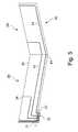
- FIG. 5is a perspective view of one half of the waveguide structure embodiment shown in FIG. 2 , shown folded into an L-configuration and ready to be engaged to a display;
- FIG. 6is a perspective view of the waveguide structure embodiment shown in FIG. 2 engaged to a display;
- FIG. 7is a top view of the waveguide structure embodiment shown in FIG. 3 engaged to a display;
- FIG. 8is a plan view of another embodiment a waveguide structure in accordance with this disclosure.
- FIG. 9is an underside view of a display showing a pair of the waveguide structure embodiments shown in FIG. 8 engaged thereto;
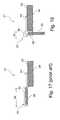
- FIG. 10is a sectional side view of one embodiment of an optical element in accordance with this disclosure shown engaged to a display and having a waveguide structure optically engaged thereto, and directing light from the waveguide across the upper surface of the display;
- FIG. 11is a view similar to FIG. 10 but showing another embodiment of an optical element in accordance with this disclosure.
- FIG. 12is a view similar to FIG. 10 but showing a further embodiment of an optical element in accordance with this disclosure
- FIG. 13is a view similar to FIG. 10 but showing yet another embodiment of an optical element in accordance with this disclosure
- FIG. 14is a sectional side view of another embodiment of an optical element in accordance with this disclosure shown engaged to a display and having a waveguide structure optically engaged thereto, wherein the waveguide structure is positioned beneath and parallel to the display;
- FIG. 15is a view similar to FIG. 14 but showing another embodiment of an optical element in accordance with this disclosure.
- FIG. 16is an exploded perspective view of a display, a waveguide structure in accordance with this disclosure and an optical element in accordance with this disclosure;
- FIG. 17is a sectional side view of a prior art waveguide-based optical touch input device showing the relatively wide bezel dimension required to accommodate the waveguide structure and associated optics;
- FIG. 18is a sectional side view of the combined waveguide structure and optical element of one embodiment engaged to a display showing the relatively reduced bezel dimensions required;
- FIGS. 19( a ) and 19 ( b )show plan and side views of a typical prior art assembly of a transmit waveguide and an external vertical collimating lens.
- a waveguide structure 20 for an input device in the form of a touch screen 21is formed as a substantially two-dimensional sheet comprising a plurality of waveguides adapted to carry input signals or output signals for the touch screen 21 .
- the touch screen 21is substantially rectangular in shape and includes a substantially planar input surface 23 for receiving user input, such as the touch of a finger or a stylus.
- the input surface 23coincides with the outer surface of a display 24 (such as a liquid crystal display (LCD)).
- the input surfacemay coincide with the outer surface of a transparent protective cover in front of a display.
- the substantially rectangular waveguide structure 20is formed from a resilient plastics material that is substantially flexible.
- the waveguide structure 20is repeatably and reversibly bendable through at least 90° without being mechanically damaged.
- FIG. 5shows one half of the waveguide structure 20 shown in FIG. 2 folded into an L-configuration and ready to be engaged to a display.
- FIG. 6shows the entire waveguide structure 20 of FIG. 2 engaged to the periphery 25 of a display 24
- FIG. 7shows waveguide structure 20 of FIG. 3 or FIG. 4 engaged to the periphery 25 of a display 24 .
- FIG. 5shows one half of
- the waveguide structure 20is configured as an ‘L’, rather than a substantially rectangular sheet as shown in FIGS. 2 to 4 . This embodiment is particularly useful when, as shown in FIG. 9 , the waveguide structure is engaged to the underside of a display 24 .
- the waveguide structure 20preferably comprises a plurality of optical waveguides comprising a photo-curable polymer material fabricated on a flexible polymer substrate, for example by a method disclosed in U.S. patent application Ser. No. 11/742,194 entitled ‘Methods for fabricating polymer optical waveguides on large area panels’. Briefly, this document describes methods for fabricating polymer optical waveguides comprising a three layer structure, wherein at least one of the optical layers is deposited by a two-stage deposition process whereby the second step is a spinning process.
- the invention disclosed in U.S. Ser. No. 11/742,194is of particular relevance to the volume production of polymer optical waveguides on large area substrates.
- the waveguide structure 20is configured such that, in use, the waveguide structure 20 extends around at least a portion of the periphery 25 of a display 24 .
- the waveguide structure 20extends around the entire periphery 25 and is disposed substantially perpendicularly to the input surface 23 of a touch screen 21 .
- the waveguide structure 20is engaged to a touch screen 21 such that each of the waveguides 10 , 14 extends entirely below the input surface 23 of the touch screen.
- the waveguide structure 20is a two-dimensional sheet that extends underneath and substantially parallel to the input surface 23 of a touch screen 21 .
- One such configurationcomprises four waveguide structures 20 , each extending along an edge of the touch screen 21 .
- the waveguide structure 20is formed on a pair of L-shaped substrates 26 that extend underneath and substantially parallel to the input surface 23 of a touch screen 21 . It will be appreciated that preferably the L-shaped substrates 26 lie substantially within the periphery 25 of the touch screen. However, the L-shaped substrates could also exceed the periphery 25 of the touch screen.
- the waveguide structures 20may lie underneath as well as extend along at least a portion of the periphery 25 of a touch screen 21 , however, not extend above the input surface 23 of the touch screen. Irrespective of the particular embodiment, it will be understood that the disclosed waveguide structures 20 are configured such that, in use, the waveguides pass through a maximum of two mutually perpendicular planes.
- the waveguide structure 20comprises a plurality of transmit waveguides 10 adapted to carry a plurality of light signals from a light source 11 , and a plurality of receive waveguides 14 adapted to carry a plurality of output signals to a multi-element detector 15 .
- the transmit waveguides 10are grouped on the waveguide structure 20 to define a transmit section 28
- the receive waveguides 14are grouped to define a receive section 29 .
- Each of the waveguides 10 and 14includes an input portion for receiving an input signal and an output portion for transmitting an output signal.
- the transmit and receive waveguides 10 and 14are positioned on the waveguide structure 20 such that the input portions 30 of the transmit waveguides 10 and the output portions 31 of the receive waveguides 14 are disposed on or proximate to a first side 32 of the waveguide structure 20 , and the output portions 33 of the transmit waveguides 10 and the input portions 34 of the receive waveguides 14 are disposed on or proximate to a second side 35 of the waveguide structure 20 , the first and second sides 32 and 35 being mutually opposed.
- the input portions 30 of the transmit waveguides 10are grouped into an input array 36
- the output portions 31 of the receive waveguides 14are grouped together into an output array 37 , with each array 36 and 37 extending along only a portion of the first side 32 for coupling with a source 11 or detector 15 respectively.
- the input array 36 of transmit waveguides 10may include a splitter 18 for distribution of optical power to the transmit waveguides 10 .
- the output portions 33 of the transmit waveguides 10 and the input portions 34 of the receive waveguides 14are spaced, preferably substantially evenly spaced, along substantially the entire length of the second side 35 . However, it will be appreciated that the spacing may be selected for the particular application. It will be further appreciated that for clarity, only a few transmit waveguides 10 or receive waveguides 14 are shown in each of FIGS. 2 to 6 and 8 to 9 .
- the waveguidesare positioned such that the input portions 30 of the transmit waveguides 10 and the output portions 31 of the receive waveguides 14 are disposed on or proximate to opposite sides of the waveguide structure 20 .
- the output portions 33 of the transmit waveguides 10 and the input portions 34 of the receive waveguides 14are disposed on or proximate to a common side 35 of the waveguide structure 20 and spaced along substantially the entire length of the common side.
- the waveguidesare substantially evenly spaced, however it will be appreciated that the spacing may be selected for the particular application.
- the input array 36is optically coupleable with a light source 11 for supplying a light signal and the output array 37 is optically coupleable with a suitable multi-element light detector 15 .
- the lighthas a predetermined wavelength that may, for example, be in the infrared region of the spectrum, preferably between 700 and 1000 nm. Alternatively, the predetermined wavelength may be in the visible region of the spectrum.
- the output array 37is disposed at the terminus of one leg of the L-shaped waveguide structure 20 , and the input portions 34 of the receive waveguides 14 are substantially evenly spaced along substantially the entire length of the two outer edges 39 of the L-shaped substrate 26 , thereby to define an L-shaped receive section. It will be appreciated that, apart from the inclusion of an optical splitter 18 , an essentially identical arrangement to that shown in FIG. 8 would function as a transmit L-shaped waveguide structure.
- waveguide structurescan be overlapped to ensure that the entire periphery 25 of a touch screen 21 is accessible to either the transmit section 28 or receive section 29 of a waveguide structure 20 .
- the waveguide structures shown in FIG. 3 and FIG. 4can be folded around the periphery 25 of the touch screen 21 with a source 11 and a detector 15 overlapped in one corner, as clearly shown in FIG. 7 .
- a source 11 and detector 15could be located on a single chip.
- the waveguide structure shown in FIG. 2requires a source 11 and a detector 15 to be located below the touch screen 21
- the waveguide structures shown in FIGS. 3 and 4allow a source 11 and a detector 15 to be located beside the touch screen 21 .
- the receive-side waveguide structure shown in FIG. 8 and a similar transmit-side waveguide structurecan be engaged in overlapping fashion to the underside of a display 24 , as shown in FIG. 9 . It will be appreciated that this overlapping arrangement may require a degree of flexibility in each waveguide structure for out-of-plane bending, but this will be trivial if, as preferred, the substrates 26 are composed of plastics materials.
- the waveguide structures 20 illustrated in FIGS. 2 to 6 and 8 to 9show the output portions 33 of the transmit waveguides 10 and the input portions 34 of the receive waveguides 14 extending to edge(s) 35 or 39 of each structure. In some embodiments this will indeed be the case.
- the output portions 33 or the input portions 34 (or both)each include an integral structure for collimating the light beams in the plane of the input surface 23 .
- the integral structureis in the form of a planar lens 16 , as shown in FIG. 1 and FIG. 16 .
- the integral structuremay be a planar internally reflective minor, as disclosed in U.S. Pat. No. 7,352,940, entitled ‘Waveguide design incorporating reflective optics’.
- the transmit waveguides 10 and receive waveguides 14are provided on a single substantially rectangular strip designed to be folded around the entire periphery of the touch screen. It will be appreciated that the larger the touch screen, the longer the rectangular strip needs to be, however this will be limited by the size of the substrate used for waveguide fabrication.
- the waveguide fabrication techniques disclosed in U.S. Pat. No. 7,811,640will clearly be applicable to this situation. If substrate size is a limitation it is of course possible to fabricate the transmit waveguides and receive waveguides on separate substantially rectangular strips, each of which would be folded around two sides of the periphery, for example as shown in FIG. 5 .
- a key advantage of fabricating the waveguides on rectangular strips, as shown in FIGS. 2 and 3 , compared to the prior art L-shaped waveguide structures as shown in FIG. 1is that it is significantly easier to singulate rectangular structures than L-shaped structures with a dicing saw. In particular, the interior sides of an L-shaped structure are difficult to cut with a dicing saw.
- the waveguide structure shown in FIG. 4has a recess 61 , designed to facilitate electrical connections to the touch screen 21 .
- the recess 61will complicate the singulation process, but since there are no transmit waveguide outputs 33 or receive waveguide inputs 34 along the side 62 incorporating the recess 61 , that side can be shaped with a cruder stamping process while the straight sides are diced.
- an advantage of the L-shaped configuration shown in FIG. 8 compared to the prior art L-shaped configuration shown in FIG. 1is that the inner edges 38 of the L-shaped waveguide structure having no receive waveguide inputs 34 , can be shaped with a cruder stamping process while the outer edges 39 can be diced with a dicing saw.
- the waveguide structures 20are preferably substantially flexible for assisting in folding around the periphery 25 of a touch screen 21 .
- a waveguide structure 20includes at least one fold line 41 defined by a line of weakness to assist in the installation around a touch screen 21 .
- the fold line 41is a printed mark visible to a machine vision system when the waveguide structure 20 is machine assembled with a touch screen 21 .
- the printed markmay assist with manual assembly of the waveguide structure 20 with a touch screen 21 .
- an optical element 42 for a touch screen 21comprising a first reflective surface 43 for reflecting a light signal 44 in a direction substantially parallel to the input surface 23 , coincident with the outer surface of a display 24 , and a connect portion 45 adapted for connection to the waveguide structure 20 .
- the optical element 42is configured for use with a touch screen 21 such that, in use, the first reflective surface 43 is positioned above the input surface 23 of a touch screen 21 to re-direct a light signal 44 to or from the waveguide structure 20 .
- the connect portion 45is at least partially below the input surface 23 .
- the optical element 42further includes a body of light transmissive material 46 for transmission of a light signal 44 between the connect portion 45 and the first reflective surface 43 .
- the optical element 42further includes a second reflective surface 47 that, in use, is positioned below the input surface 23 , and where the waveguide structure 20 extends underneath and substantially parallel to the input surface.
- an optical element 42could be constructed such that one or both of the reflective surfaces are externally reflective (i.e. conventional) mirrors rather than internally reflective surfaces.
- an optical element 42has internally reflective surfaces, as shown for example in FIGS. 10 to 15 , is preferred for robustness and ease of manufacture (by injection moulding for example).
- an externally reflective mirrorwould need to be metallised, whereas the internally reflective surfaces may not need to be metallised if the condition for total internal reflection is met. Those skilled in the art will understand that this can be ensured by appropriate design of the optical element.
- an optical element 42may be formed as an elongate strip of plastics material substantially transparent to the signal light (e.g. infrared light). Desirably, the optical element 42 is opaque to light of other wavelengths (e.g. ambient visible light if the signal comprises infrared light).
- the optical element 42may be injection moulded or extruded and may be substantially rigid.
- the first internally reflective surface 43may be curved thereby to focus a light signal 44 in a direction substantially perpendicular to the plane of the input surface 23 , as shown for example in FIGS. 10 to 12 and 15 .
- the first reflective surface 43may be planar, as shown for example in FIGS. 13 and 14 .
- the second reflective surface 47where present, may likewise be curved or planar. If either the first or second reflective surfaces are curved, they are preferably curved in a cylindrical fashion so as to focus a plurality of signals associated with a plurality of waveguides.
- the optical element 42has an optical surface 48 through which light 44 passes as it transits a touch screen 21 .
- this optical surface 48may be planar.
- itmay be curved to form a lens portion 49 so as to focus a light signal 44 in a direction substantially perpendicular to the plane of the input surface 23 .
- the lens portion 49is curved in a cylindrical fashion so as to focus a plurality of signals associated with a plurality of waveguides.
- the optical element 42may be shaped such that, in use, the exterior angle between the input surface 23 and the optical surface 48 is greater than or equal to 90° (as shown in FIGS. 10 , 12 , 13 and 15 for example), to minimise the build-up of dirt over time which could potentially obscure the optical surface 48 .
- optical elements engaged to the transmit and receive sections of the waveguide structurehave different optical surfaces.
- the transmit-side optical elementsmay have a planar optical surface 48 and the receive-side optical elements may have an optical surface in the form of a lens 49 .
- the optical element 42includes a recess 50 such that the optical element 42 is releasably attachable to a display 24 .
- the optical element 42is configured as a single piece having physical dimensions matching the periphery 25 of a display 24 such that the optical element 42 is adapted to ‘clip’ onto the display.
- the optical element 42can be glued onto a display 24 .
- the optical element 42may be configured as two L-shaped pieces each adapted to clip around two adjacent sides of a display, or as four straight pieces each adapted to be attached to one side of a display 24 (as shown in FIG. 16 ).
- the waveguide structure 20may be fixedly attached to the optical element 42 by gluing. However, it will be appreciated that any method of attachment that provides sufficient and stable optical communication between the waveguides 10 , 14 and the optical element 42 will be suitable.
- FIG. 13A particularly preferred design for an optical element 42 is shown in FIG. 13 , with an internally reflective surface 43 , a recess 50 and an optical surface 48 comprising a lens portion 49 .
- the internally reflective surface 43is a plane surface inclined at an angle 61 of 49° to the horizontal, and the lens portion 49 forms an exterior angle of approximately 90° with the input surface 23 such that there is no re-entrant cavity between the two where dirt may collect. Because the internally reflective surface 43 is angled at 49° to the horizontal, instead of 45°, the lens portion 49 is still able to collimate the signal light 44 parallel to the input surface 23 .
- the dimensions 62 , 63 , 64 , 65 , 66 , 67 and 68 of the optical element 42are 3.9 mm, 10 mm, 4.4 mm, 30 mm, 6 mm, 6.4 mm and 3.6 mm respectively, and the lens portion 49 has a radius of curvature of 7.2 mm.
- the waveguide structure 20is oriented such that its waveguides are on the surface adjacent to the connect portion 45 .
- an apparatus for use in an input devicecomprising a touch screen 21 , a pair of waveguide structures 20 , and four optical elements 42 .
- the pair of waveguide structures 20correspond to a transmit waveguide structure and a receive waveguide structure which, together, extend along substantially the entire periphery 25 of a display 24 .
- the four optical elements 42are engaged to the waveguide structures 20 in use and are in optical communication with respective waveguides of the waveguide structures 20 .
- a pair of L-shaped optical elements, or a one-piece optical elementwould also be suitable.
- each of the optical elements 42extends from a position below the input surface 23 to a position above the input surface 23 such that each optical element 42 transmits input or output signals to or from the input area 13 of a touch screen 21 between respective waveguides of the waveguide structures 20 , which extend entirely below the input surface 23 .
- the planar lenses 16 of each waveguidecan be seen in FIG. 16 . These lenses 16 collimate light into and from the optical elements 42 , such that signal beams passing across the input surface 23 of a touch screen 21 are focused in the plane of the input surface.
- the waveguide structures 20are positioned between the display 24 and the optical elements 42 .
- a method of transmitting input and output signals for a touch screen devicecomprises providing a waveguide structure 20 , providing one or more optical elements 42 , and then optically coupling the waveguide structure 20 with a respective optical element 42 such that, in use, each optical element 42 transmits input or output signals to or from the input area 13 of a touch screen 21 to a respective waveguide of a waveguide structure 20 extending entirely below the input surface 23 .
- a disclosed method of reducing the width 54 of a bezel 51 in a touch screen 21comprises providing a waveguide structure 20 , providing one or more optical elements 42 , and then optically coupling the waveguide structure 20 with a respective optical element 42 such that, in use, each the optical element 42 transmits an input or output signal 44 to or from the waveguide structure 20 .
- the optical elements 42extend from above the input surface 23 to a position below the input surface and the waveguides of each waveguide structure 20 are terminated at a position below the input surface.
- the disclosed structures and methodsprovide a substantially reduced bezel dimension 54 ( FIG. 18 ) compared with prior art devices ( FIG. 17 ).
- the bezel requirements( FIG. 18 ) essentially comprise a thin raised ‘lip’ 52 surrounding a display 24 .
- the bezel requirements for prior art devices( FIG. 17 ) comprise a relatively wide raised flange 53 surrounding a display 24 .
- FIGS. 19( a ) and 19 ( b )show plan and side views of a typical prior art assembly of an output portion 33 of a transmit waveguide 10 having an external vertical collimating lens (VCL) 17 , wherein the transmit waveguide 10 and VCL 17 are mounted on a common base 71 .
- VCLvertical collimating lens
- a transmit waveguide 10comprises a substrate 72 , a lower cladding layer 73 , a core layer 74 and an upper cladding layer 75 , with the core layer 74 terminating with an integrated planar lens 16 that collimates the light signal 44 in the plane of an adjoining input area.
- the substrate 72 , lower cladding layer 73 and upper cladding layer 75have been omitted from FIG. 19 a .
- a light signal 44 launched from the end face 76 of a planar lens 16will diverge in the direction perpendicular to the plane of the input area. As a consequence it is often desirable for the light signal 44 to be focussed in this direction as well.
- VCL 17The VCL is generally curved in a cylindrical fashion so as to focus a plurality of signals associated with a plurality of waveguides.
- the gap 77 between the end face 76 of the planar lens 16 and the curved face 78 of a VCL 17contributes to the overall bezel width in a prior art device, and should ideally be minimised.
- the VCLto be a relatively powerful lens, i.e. to have a small radius of curvature.
- Those skilled in the art of micro-opticswill understand that such a high magnification optical system is extremely susceptible to errors in the design and manufacture of a VCL, and in its placement with respect to the waveguides.
- ‘out of plane’ focussingvia an optical element 42 , as shown in FIGS. 10 to 15 .
- ‘out of plane’ focusingmay be provided by a lens portion 49 , a first reflective surface 43 , a second reflective surface 47 or a combination of the above.
- Particularly notableare the embodiments shown in FIGS. 13 and 14 , where ‘out of plane’ focussing is provided by a lens portion 49 , such that the distance between the waveguides in the waveguide structure 20 and the lens portion 49 is greatly increased compared to the gap 77 of the prior art device.
- An optical element 42may be designed such that two or more of the lens portion 49 , first reflective surface 43 and second reflective surface 47 provide the ‘out of plane’ focussing in combination, as shown for example in FIG. 11 . Such an arrangement may further relax the tolerances required for the optical element, since an optical system comprising two or more weaker focussing elements in series is generally more tolerant to alignment ‘errors’ than a system of equivalent magnification comprising a single relatively more powerful optical element.
- the waveguide structures and optical elementscould be used on the transmit side of an optical input device, and with the receive waveguides 14 and multi-element detector 15 replaced by one or more arrays of discrete detectors.
Landscapes
- Engineering & Computer Science (AREA)
- General Engineering & Computer Science (AREA)
- Theoretical Computer Science (AREA)
- Human Computer Interaction (AREA)
- Physics & Mathematics (AREA)
- General Physics & Mathematics (AREA)
- Position Input By Displaying (AREA)
- Optical Integrated Circuits (AREA)
Abstract
Description
- 1.) Mounting the waveguide structure and the disclosed optical element to a touch screen allows the bezel dimensions to be relatively reduced compared to prior art devices.
- 2.) The waveguide structures provide a number of cost savings compared to prior art L-shaped waveguide structures. For example, from a manufacturing perspective it is relatively simpler to singulate a waveguide structure configured in rectangular strips than an L-shaped waveguide structure.
- 3.) Assembling a disclosed input device utilising the waveguide structures and optical elements is relatively cheaper compared to prior art devices. Additionally, the disclosed techniques require relatively fewer components than prior art devices.
- 4.) The configurations of the disclosed structures mean that the source and detector can be physically located adjacent to each other or, preferably, on the same chip. This simplifies the layout of the internals of the input device and reduces production costs.
- 5.) From an aesthetics perspective, a thin bezel ‘lip’ surrounding the touch screen is more appealing than a relatively wide flange surrounding the touch screen.
- 6.) The optical element with the waveguide structure attached thereto can be fabricated as a single unit having physical dimensions matching the periphery of the touch screen. The optical element can then be simply clipped onto the touch screen thereby avoiding alignment issues and simplifying installation and reducing the installation costs.
- 7.) The apparatus and methods disclosed herein enable a relatively larger touch screen to be provided on the device for the same overall dimensions because the bezel space requirements are now reduced. This satisfies the intent of many designers, which is to make the touch display of comparable width to the device itself. The advantage of this is that the user obtains the largest possible display size for a given device size, which is both practical and aesthetically pleasing.
- 8.) The disclosed apparatus and methods relax the tolerances on the design, manufacture and placement of optical elements used to focus the optical signals in the direction perpendicular to the input area.
- 9.) The disclosed embodiments may be used in conjunction with other transmit or receive optics. For example U.S. Pat. No. 7,099,553 discloses a touch input device where the signal light is launched across the input area by an L-shaped light pipe with a plurality of reflective facets, instead of discrete transmit-side optical waveguides
- 10.) In this sort of device, the waveguide structures and optical elements could still be used on the receive side.
Claims (24)
Applications Claiming Priority (3)
| Application Number | Priority Date | Filing Date | Title |
|---|---|---|---|
| AU2006905255AAU2006905255A0 (en) | 2006-09-22 | Waveguide configurations for optical touch systems | |
| AUAU2006905255 | 2006-09-22 | ||
| AU2006905255 | 2006-09-22 |
Publications (2)
| Publication Number | Publication Date |
|---|---|
| US20080074402A1 US20080074402A1 (en) | 2008-03-27 |
| US8674963B2true US8674963B2 (en) | 2014-03-18 |
Family
ID=39200087
Family Applications (1)
| Application Number | Title | Priority Date | Filing Date |
|---|---|---|---|
| US11/859,331Expired - Fee RelatedUS8674963B2 (en) | 2006-09-22 | 2007-09-21 | Waveguide configurations for optical touch systems |
Country Status (3)
| Country | Link |
|---|---|
| US (1) | US8674963B2 (en) |
| TW (1) | TW200823506A (en) |
| WO (1) | WO2008034184A1 (en) |
Cited By (24)
| Publication number | Priority date | Publication date | Assignee | Title |
|---|---|---|---|---|
| US20120176343A1 (en)* | 2001-11-02 | 2012-07-12 | Neonode, Inc. | Optical elements with alternating reflective lens facets |
| US20120327029A1 (en)* | 2011-06-27 | 2012-12-27 | Qualcomm Mems Technologies, Inc. | Touch input sensing using optical ranging |
| US20130021302A1 (en)* | 2011-07-22 | 2013-01-24 | Rapt Ip Limited | Optical coupler for use in an optical touch sensitive device |
| US9952719B2 (en) | 2012-05-24 | 2018-04-24 | Corning Incorporated | Waveguide-based touch system employing interference effects |
| US9950500B2 (en) | 2008-05-21 | 2018-04-24 | Manufacturing Resources International, Inc. | Glass assembly |
| US10126579B2 (en) | 2013-03-14 | 2018-11-13 | Manfuacturing Resources International, Inc. | Rigid LCD assembly |
| US10191212B2 (en) | 2013-12-02 | 2019-01-29 | Manufacturing Resources International, Inc. | Expandable light guide for backlight |
| US10228799B2 (en) | 2012-10-04 | 2019-03-12 | Corning Incorporated | Pressure sensing touch systems and methods |
| US10261362B2 (en) | 2015-09-01 | 2019-04-16 | Manufacturing Resources International, Inc. | Optical sheet tensioner |
| US10431166B2 (en) | 2009-06-03 | 2019-10-01 | Manufacturing Resources International, Inc. | Dynamic dimming LED backlight |
| US10466539B2 (en) | 2013-07-03 | 2019-11-05 | Manufacturing Resources International, Inc. | Airguide backlight assembly |
| US10527276B2 (en) | 2014-04-17 | 2020-01-07 | Manufacturing Resources International, Inc. | Rod as a lens element for light emitting diodes |
| US10649273B2 (en) | 2014-10-08 | 2020-05-12 | Manufacturing Resources International, Inc. | LED assembly for transparent liquid crystal display and static graphic |
| US11591261B2 (en) | 2008-05-21 | 2023-02-28 | Manufacturing Resources International, Inc. | Photoinitiated optical adhesive and method for using same |
| US11669210B2 (en) | 2020-09-30 | 2023-06-06 | Neonode Inc. | Optical touch sensor |
| US20230315234A1 (en)* | 2016-12-07 | 2023-10-05 | Flatfrog Laboratories Ab | Touch Device |
| US12056316B2 (en) | 2019-11-25 | 2024-08-06 | Flatfrog Laboratories Ab | Touch-sensing apparatus |
| US12055969B2 (en) | 2018-10-20 | 2024-08-06 | Flatfrog Laboratories Ab | Frame for a touch-sensitive device and tool therefor |
| US12055809B2 (en) | 2021-02-12 | 2024-08-06 | Manufacturing Resources International, Inc. | Display assembly using structural adhesive |
| US12086362B2 (en) | 2017-09-01 | 2024-09-10 | Flatfrog Laboratories Ab | Optical component |
| US12175044B2 (en) | 2017-02-06 | 2024-12-24 | Flatfrog Laboratories Ab | Optical coupling in touch-sensing systems |
| US12282653B2 (en) | 2020-02-08 | 2025-04-22 | Flatfrog Laboratories Ab | Touch apparatus with low latency interactions |
| US12350730B1 (en) | 2023-12-27 | 2025-07-08 | Manufacturing Resources International, Inc. | Bending mandril comprising ultra high molecular weight material, related bending machines, systems, and methods |
| US12429726B1 (en) | 2023-10-02 | 2025-09-30 | Manufacturing Resources International, Inc. | Optical stack with a liquid crystal layer and a micro lens array, electronic display assembly, and related methods |
Families Citing this family (56)
| Publication number | Priority date | Publication date | Assignee | Title |
|---|---|---|---|---|
| US8018440B2 (en) | 2005-12-30 | 2011-09-13 | Microsoft Corporation | Unintentional touch rejection |
| US7603001B2 (en)* | 2006-02-17 | 2009-10-13 | Qualcomm Mems Technologies, Inc. | Method and apparatus for providing back-lighting in an interferometric modulator display device |
| US7845841B2 (en)* | 2006-08-28 | 2010-12-07 | Qualcomm Mems Technologies, Inc. | Angle sweeping holographic illuminator |
| US8107155B2 (en)* | 2006-10-06 | 2012-01-31 | Qualcomm Mems Technologies, Inc. | System and method for reducing visual artifacts in displays |
| US7855827B2 (en) | 2006-10-06 | 2010-12-21 | Qualcomm Mems Technologies, Inc. | Internal optical isolation structure for integrated front or back lighting |
| US7864395B2 (en)* | 2006-10-27 | 2011-01-04 | Qualcomm Mems Technologies, Inc. | Light guide including optical scattering elements and a method of manufacture |
| WO2008077195A1 (en)* | 2006-12-27 | 2008-07-03 | Jonathan Payne | Lens configurations for optical touch systems |
| JP2008170524A (en)* | 2007-01-09 | 2008-07-24 | Nitto Denko Corp | Optical waveguide for touch panel |
| JP4847389B2 (en)* | 2007-04-11 | 2011-12-28 | 日東電工株式会社 | Optical waveguide for touch panel and touch panel using the same |
| JP2008281780A (en)* | 2007-05-10 | 2008-11-20 | Nitto Denko Corp | Optical waveguide with lens for touch panel and optical waveguide used therefor |
| JP4521025B2 (en)* | 2007-11-29 | 2010-08-11 | 日東電工株式会社 | Optical waveguide for touch panel and touch panel using the same |
| US7949213B2 (en) | 2007-12-07 | 2011-05-24 | Qualcomm Mems Technologies, Inc. | Light illumination of displays with front light guide and coupling elements |
| JP4452305B2 (en)* | 2007-12-25 | 2010-04-21 | 日東電工株式会社 | Optical waveguide for touch panel, touch panel using the same, and method for manufacturing optical waveguide for touch panel |
| US20090168459A1 (en)* | 2007-12-27 | 2009-07-02 | Qualcomm Incorporated | Light guide including conjugate film |
| RU2519392C2 (en)* | 2008-01-11 | 2014-06-10 | О-Нэт Вэйв Тач Лимитед | Sensor device |
| WO2009102731A2 (en) | 2008-02-12 | 2009-08-20 | Qualcomm Mems Technologies, Inc. | Devices and methods for enhancing brightness of displays using angle conversion layers |
| JP4966228B2 (en)* | 2008-03-10 | 2012-07-04 | 日東電工株式会社 | Optical waveguide for touch panel and touch panel using the same |
| US20090256811A1 (en)* | 2008-04-15 | 2009-10-15 | Sony Ericsson Mobile Communications Ab | Optical touch screen |
| WO2009129264A1 (en) | 2008-04-15 | 2009-10-22 | Qualcomm Mems Technologies, Inc. | Light with bi-directional propagation |
| US8553014B2 (en) | 2008-06-19 | 2013-10-08 | Neonode Inc. | Optical touch screen systems using total internal reflection |
| US8676007B2 (en)* | 2008-06-19 | 2014-03-18 | Neonode Inc. | Light-based touch surface with curved borders and sloping bezel |
| JP5210074B2 (en)* | 2008-07-29 | 2013-06-12 | 日東電工株式会社 | Optical waveguide for three-dimensional sensor and three-dimensional sensor using the same |
| US8172417B2 (en)* | 2009-03-06 | 2012-05-08 | Qualcomm Mems Technologies, Inc. | Shaped frontlight reflector for use with display |
| US20100195310A1 (en)* | 2009-02-04 | 2010-08-05 | Qualcomm Mems Technologies, Inc. | Shaped frontlight reflector for use with display |
| US9158416B2 (en) | 2009-02-15 | 2015-10-13 | Neonode Inc. | Resilient light-based touch surface |
| CN102449512A (en) | 2009-05-29 | 2012-05-09 | 高通Mems科技公司 | Illumination devices and methods of fabrication thereof |
| TWI405109B (en)* | 2009-07-03 | 2013-08-11 | Pixart Imaging Inc | Optical touch display |
| TWI436253B (en)* | 2009-07-16 | 2014-05-01 | Raydium Semiconductor Corp | Optical touch apparatus and operating method thereof |
| US8261213B2 (en) | 2010-01-28 | 2012-09-04 | Microsoft Corporation | Brush, carbon-copy, and fill gestures |
| US9411504B2 (en) | 2010-01-28 | 2016-08-09 | Microsoft Technology Licensing, Llc | Copy and staple gestures |
| US9519356B2 (en) | 2010-02-04 | 2016-12-13 | Microsoft Technology Licensing, Llc | Link gestures |
| US9965165B2 (en) | 2010-02-19 | 2018-05-08 | Microsoft Technology Licensing, Llc | Multi-finger gestures |
| US9310994B2 (en)* | 2010-02-19 | 2016-04-12 | Microsoft Technology Licensing, Llc | Use of bezel as an input mechanism |
| US9367205B2 (en) | 2010-02-19 | 2016-06-14 | Microsoft Technolgoy Licensing, Llc | Radial menus with bezel gestures |
| US9454304B2 (en) | 2010-02-25 | 2016-09-27 | Microsoft Technology Licensing, Llc | Multi-screen dual tap gesture |
| EP2388630A1 (en)* | 2010-05-21 | 2011-11-23 | Nitto Denko Corporation | Optical waveguide with a cladding having lower transmittance in visible than near-infrared wavelength range and its use in an optical touch panel |
| JP2011253095A (en)* | 2010-06-03 | 2011-12-15 | Nitto Denko Corp | L-shaped optical waveguide device |
| TWI407351B (en)* | 2010-06-04 | 2013-09-01 | Hon Hai Prec Ind Co Ltd | Electronic device having infrared touching panel |
| TWI423098B (en)* | 2010-07-15 | 2014-01-11 | Quanta Comp Inc | Optical touch structure |
| US8902484B2 (en) | 2010-12-15 | 2014-12-02 | Qualcomm Mems Technologies, Inc. | Holographic brightness enhancement film |
| SG11201403772QA (en)* | 2012-01-29 | 2014-09-26 | Neonode Inc | Light-based touch surface with curved borders and sloping bezel |
| US20130203470A1 (en)* | 2012-02-02 | 2013-08-08 | Ultra-Scan Corporation | Protective Display Surface |
| EP2689320B1 (en)* | 2012-03-11 | 2016-02-03 | Neonode Inc. | Optical touch screen using total internal reflection |
| US9939905B2 (en)* | 2012-11-09 | 2018-04-10 | Ross Conrad Labelson | Optical control of display screens |
| US9582122B2 (en) | 2012-11-12 | 2017-02-28 | Microsoft Technology Licensing, Llc | Touch-sensitive bezel techniques |
| US9477337B2 (en) | 2014-03-14 | 2016-10-25 | Microsoft Technology Licensing, Llc | Conductive trace routing for display and bezel sensors |
| EP3250993B1 (en) | 2015-01-28 | 2019-09-04 | FlatFrog Laboratories AB | Dynamic touch quarantine frames |
| US10496227B2 (en) | 2015-02-09 | 2019-12-03 | Flatfrog Laboratories Ab | Optical touch system comprising means for projecting and detecting light beams above and inside a transmissive panel |
| EP4075246B1 (en) | 2015-12-09 | 2024-07-03 | FlatFrog Laboratories AB | Stylus for optical touch system |
| EP3545392A4 (en) | 2016-11-24 | 2020-07-29 | FlatFrog Laboratories AB | AUTOMATIC OPTIMIZATION OF TOUCH SIGNALS |
| US10606414B2 (en) | 2017-03-22 | 2020-03-31 | Flatfrog Laboratories Ab | Eraser for touch displays |
| EP4036697A1 (en) | 2017-03-28 | 2022-08-03 | FlatFrog Laboratories AB | Optical touch sensing apparatus |
| WO2019172826A1 (en) | 2018-03-05 | 2019-09-12 | Flatfrog Laboratories Ab | Improved touch-sensing apparatus |
| WO2020153890A1 (en) | 2019-01-25 | 2020-07-30 | Flatfrog Laboratories Ab | A videoconferencing terminal and method of operating the same |
| US11893189B2 (en) | 2020-02-10 | 2024-02-06 | Flatfrog Laboratories Ab | Touch-sensing apparatus |
| CN115469404B (en)* | 2022-04-20 | 2024-11-29 | 大连理工大学 | Two-dimensional high-speed photoelectric conversion array chip |
Citations (24)
| Publication number | Priority date | Publication date | Assignee | Title |
|---|---|---|---|---|
| US3478220A (en) | 1966-05-11 | 1969-11-11 | Us Navy | Electro-optic cursor manipulator with associated logic circuitry |
| US3673327A (en) | 1970-11-02 | 1972-06-27 | Atomic Energy Commission | Touch actuable data input panel assembly |
| JPS6376012A (en) | 1986-09-19 | 1988-04-06 | Matsushita Electric Ind Co Ltd | Coordinate position input device |
| US4988893A (en) | 1986-12-30 | 1991-01-29 | International Business Machines Corporation | Latch cell family in CMOS technology gate array |
| US5196836A (en) | 1991-06-28 | 1993-03-23 | International Business Machines Corporation | Touch panel display |
| US5914709A (en) | 1997-03-14 | 1999-06-22 | Poa Sana, Llc | User input device for a computer system |
| US6181842B1 (en) | 2000-01-10 | 2001-01-30 | Poa Sana, Inc. | Position digitizer waveguide array with integrated collimating optics |
| US20040201579A1 (en)* | 2003-04-08 | 2004-10-14 | Poa Sana, Inc., A California Corporation | Apparatus and method for a data input device using a light lamina screen and an optical position digitizer |
| US20050201681A1 (en) | 2004-01-15 | 2005-09-15 | National Semiconductor Corporation | Hybrid waveguide |
| US20050271319A1 (en) | 2004-06-04 | 2005-12-08 | National Semiconductor Corporation, A Delaware Corporation | Apparatus and method for a molded waveguide for use with touch screen displays |
| US20050271326A1 (en) | 2004-06-04 | 2005-12-08 | National Semiconductor Corporation | Waveguide with a three-dimensional lens |
| US20060002655A1 (en) | 2004-06-30 | 2006-01-05 | National Semiconductor Corporation, A Delaware Corporation | Apparatus and method for making flexible waveguide substrates for use with light based touch screens |
| US20060001654A1 (en) | 2004-06-30 | 2006-01-05 | National Semiconductor Corporation | Apparatus and method for performing data entry with light based touch screen displays |
| US20060001653A1 (en) | 2004-06-30 | 2006-01-05 | National Semiconductor Corporation | Apparatus and method for a folded optical element waveguide for use with light based touch screens |
| US6992659B2 (en) | 2001-05-22 | 2006-01-31 | Palmone, Inc. | High transparency integrated enclosure touch screen assembly for a portable hand held device |
| US20060114244A1 (en) | 2004-11-30 | 2006-06-01 | Saxena Kuldeep K | Touch input system using light guides |
| US7099553B1 (en) | 2003-04-08 | 2006-08-29 | Poa Sona, Inc. | Apparatus and method for generating a lamina of light |
| US20070024598A1 (en) | 2005-07-29 | 2007-02-01 | Miller Jeffrey N | Methods and systems for detecting selections on a touch screen display |
| US20070165008A1 (en) | 2006-01-17 | 2007-07-19 | International Business Machines Corporation | Compact infrared touch screen apparatus |
| US7267930B2 (en) | 2004-06-04 | 2007-09-11 | National Semiconductor Corporation | Techniques for manufacturing a waveguide with a three-dimensional lens |
| US7352940B2 (en)* | 2005-02-07 | 2008-04-01 | Rpo Pty Limited | Waveguide design incorporating reflective optics |
| US7369724B2 (en) | 2006-10-03 | 2008-05-06 | National Semiconductor Corporation | Apparatus and method for an improved lens structure for polymer wave guides which maximizes free space light coupling |
| US20100259508A1 (en)* | 2009-04-09 | 2010-10-14 | Nitto Denko Corporation | Optical waveguide with photoelectric conversion element and optical touch panel |
| US8023780B2 (en)* | 2008-11-18 | 2011-09-20 | Nitto Denko Corporation | Touch panel |
- 2007
- 2007-09-20WOPCT/AU2007/001390patent/WO2008034184A1/enactiveApplication Filing
- 2007-09-21USUS11/859,331patent/US8674963B2/ennot_activeExpired - Fee Related
- 2007-09-21TWTW096135515Apatent/TW200823506A/enunknown
Patent Citations (30)
| Publication number | Priority date | Publication date | Assignee | Title |
|---|---|---|---|---|
| US3478220A (en) | 1966-05-11 | 1969-11-11 | Us Navy | Electro-optic cursor manipulator with associated logic circuitry |
| US3673327A (en) | 1970-11-02 | 1972-06-27 | Atomic Energy Commission | Touch actuable data input panel assembly |
| JPS6376012A (en) | 1986-09-19 | 1988-04-06 | Matsushita Electric Ind Co Ltd | Coordinate position input device |
| US4988893A (en) | 1986-12-30 | 1991-01-29 | International Business Machines Corporation | Latch cell family in CMOS technology gate array |
| US5196836A (en) | 1991-06-28 | 1993-03-23 | International Business Machines Corporation | Touch panel display |
| US20020088930A1 (en) | 1997-03-14 | 2002-07-11 | Graham David S. | User input device for a computer system |
| US5914709A (en) | 1997-03-14 | 1999-06-22 | Poa Sana, Llc | User input device for a computer system |
| US6351260B1 (en) | 1997-03-14 | 2002-02-26 | Poa Sana, Inc. | User input device for a computer system |
| US6181842B1 (en) | 2000-01-10 | 2001-01-30 | Poa Sana, Inc. | Position digitizer waveguide array with integrated collimating optics |
| US6992659B2 (en) | 2001-05-22 | 2006-01-31 | Palmone, Inc. | High transparency integrated enclosure touch screen assembly for a portable hand held device |
| US7099553B1 (en) | 2003-04-08 | 2006-08-29 | Poa Sona, Inc. | Apparatus and method for generating a lamina of light |
| US20040201579A1 (en)* | 2003-04-08 | 2004-10-14 | Poa Sana, Inc., A California Corporation | Apparatus and method for a data input device using a light lamina screen and an optical position digitizer |
| US7786983B2 (en)* | 2003-04-08 | 2010-08-31 | Poa Sana Liquidating Trust | Apparatus and method for a data input device using a light lamina screen |
| US20050201681A1 (en) | 2004-01-15 | 2005-09-15 | National Semiconductor Corporation | Hybrid waveguide |
| US20050271326A1 (en) | 2004-06-04 | 2005-12-08 | National Semiconductor Corporation | Waveguide with a three-dimensional lens |
| US7471865B2 (en)* | 2004-06-04 | 2008-12-30 | Poa Sana Liquidating Trust | Apparatus and method for a molded waveguide for use with touch screen displays |
| US20050271319A1 (en) | 2004-06-04 | 2005-12-08 | National Semiconductor Corporation, A Delaware Corporation | Apparatus and method for a molded waveguide for use with touch screen displays |
| US7267930B2 (en) | 2004-06-04 | 2007-09-11 | National Semiconductor Corporation | Techniques for manufacturing a waveguide with a three-dimensional lens |
| US20070154133A1 (en) | 2004-06-04 | 2007-07-05 | National Semiconductor Corporation | Apparatus and method for a molded waveguide for use with touch screen displays |
| US20060001654A1 (en) | 2004-06-30 | 2006-01-05 | National Semiconductor Corporation | Apparatus and method for performing data entry with light based touch screen displays |
| US7412119B2 (en)* | 2004-06-30 | 2008-08-12 | Poa Sana Liquidating Trust | Apparatus and method for making flexible waveguide substrates for use with light based touch screens |
| US20060001653A1 (en) | 2004-06-30 | 2006-01-05 | National Semiconductor Corporation | Apparatus and method for a folded optical element waveguide for use with light based touch screens |
| US20060002655A1 (en) | 2004-06-30 | 2006-01-05 | National Semiconductor Corporation, A Delaware Corporation | Apparatus and method for making flexible waveguide substrates for use with light based touch screens |
| US20060114244A1 (en) | 2004-11-30 | 2006-06-01 | Saxena Kuldeep K | Touch input system using light guides |
| US7352940B2 (en)* | 2005-02-07 | 2008-04-01 | Rpo Pty Limited | Waveguide design incorporating reflective optics |
| US20070024598A1 (en) | 2005-07-29 | 2007-02-01 | Miller Jeffrey N | Methods and systems for detecting selections on a touch screen display |
| US20070165008A1 (en) | 2006-01-17 | 2007-07-19 | International Business Machines Corporation | Compact infrared touch screen apparatus |
| US7369724B2 (en) | 2006-10-03 | 2008-05-06 | National Semiconductor Corporation | Apparatus and method for an improved lens structure for polymer wave guides which maximizes free space light coupling |
| US8023780B2 (en)* | 2008-11-18 | 2011-09-20 | Nitto Denko Corporation | Touch panel |
| US20100259508A1 (en)* | 2009-04-09 | 2010-10-14 | Nitto Denko Corporation | Optical waveguide with photoelectric conversion element and optical touch panel |
Non-Patent Citations (1)
| Title |
|---|
| Payne, U.S. Appl. No. 11/965,230. |
Cited By (40)
| Publication number | Priority date | Publication date | Assignee | Title |
|---|---|---|---|---|
| US9052777B2 (en)* | 2001-11-02 | 2015-06-09 | Neonode Inc. | Optical elements with alternating reflective lens facets |
| US20120176343A1 (en)* | 2001-11-02 | 2012-07-12 | Neonode, Inc. | Optical elements with alternating reflective lens facets |
| US12071372B2 (en) | 2008-05-21 | 2024-08-27 | Manufacturing Resources International, Inc. | Photoinitiated optical adhesive and method for using same |
| US11591261B2 (en) | 2008-05-21 | 2023-02-28 | Manufacturing Resources International, Inc. | Photoinitiated optical adhesive and method for using same |
| US9950500B2 (en) | 2008-05-21 | 2018-04-24 | Manufacturing Resources International, Inc. | Glass assembly |
| US10730269B2 (en) | 2008-05-21 | 2020-08-04 | Manufacturing Resources International, Inc. | Glass assembly |
| US10431166B2 (en) | 2009-06-03 | 2019-10-01 | Manufacturing Resources International, Inc. | Dynamic dimming LED backlight |
| US20120327029A1 (en)* | 2011-06-27 | 2012-12-27 | Qualcomm Mems Technologies, Inc. | Touch input sensing using optical ranging |
| US20130021302A1 (en)* | 2011-07-22 | 2013-01-24 | Rapt Ip Limited | Optical coupler for use in an optical touch sensitive device |
| US9170683B2 (en)* | 2011-07-22 | 2015-10-27 | Rapt Ip Limited | Optical coupler for use in an optical touch sensitive device |
| US9952719B2 (en) | 2012-05-24 | 2018-04-24 | Corning Incorporated | Waveguide-based touch system employing interference effects |
| US10572071B2 (en) | 2012-05-24 | 2020-02-25 | Corning Incorporated | Waveguide-based touch system employing interference effects |
| US10228799B2 (en) | 2012-10-04 | 2019-03-12 | Corning Incorporated | Pressure sensing touch systems and methods |
| US10831050B2 (en) | 2013-03-14 | 2020-11-10 | Manufacturing Resources International, Inc. | Rigid LCD assembly |
| US10126579B2 (en) | 2013-03-14 | 2018-11-13 | Manfuacturing Resources International, Inc. | Rigid LCD assembly |
| US10466539B2 (en) | 2013-07-03 | 2019-11-05 | Manufacturing Resources International, Inc. | Airguide backlight assembly |
| US10191212B2 (en) | 2013-12-02 | 2019-01-29 | Manufacturing Resources International, Inc. | Expandable light guide for backlight |
| US10921510B2 (en) | 2013-12-02 | 2021-02-16 | Manufacturing Resources International, Inc. | Expandable light guide for backlight |
| US10527276B2 (en) | 2014-04-17 | 2020-01-07 | Manufacturing Resources International, Inc. | Rod as a lens element for light emitting diodes |
| US10649273B2 (en) | 2014-10-08 | 2020-05-12 | Manufacturing Resources International, Inc. | LED assembly for transparent liquid crystal display and static graphic |
| US12032240B2 (en) | 2014-10-08 | 2024-07-09 | Manufacturing Resources International, Inc. | Display system for refrigerated display case |
| US11474393B2 (en) | 2014-10-08 | 2022-10-18 | Manufacturing Resources International, Inc. | Lighting assembly for electronic display and graphic |
| US11275269B2 (en) | 2015-09-01 | 2022-03-15 | Manufacturing Resources International, Inc. | Optical sheet tensioning device |
| US10261362B2 (en) | 2015-09-01 | 2019-04-16 | Manufacturing Resources International, Inc. | Optical sheet tensioner |
| US11656498B2 (en) | 2015-09-01 | 2023-05-23 | Manufacturing Resources International, Inc. | Optical sheet tensioning device |
| US10768483B2 (en) | 2015-09-01 | 2020-09-08 | Manufacturing Resources International, Inc. | Optical sheet tensioning device |
| US20230315234A1 (en)* | 2016-12-07 | 2023-10-05 | Flatfrog Laboratories Ab | Touch Device |
| US11868568B2 (en)* | 2016-12-07 | 2024-01-09 | Flatfrog Laboratories Ab | Touch device |
| US12175044B2 (en) | 2017-02-06 | 2024-12-24 | Flatfrog Laboratories Ab | Optical coupling in touch-sensing systems |
| US12086362B2 (en) | 2017-09-01 | 2024-09-10 | Flatfrog Laboratories Ab | Optical component |
| US12055969B2 (en) | 2018-10-20 | 2024-08-06 | Flatfrog Laboratories Ab | Frame for a touch-sensitive device and tool therefor |
| US12056316B2 (en) | 2019-11-25 | 2024-08-06 | Flatfrog Laboratories Ab | Touch-sensing apparatus |
| US12282653B2 (en) | 2020-02-08 | 2025-04-22 | Flatfrog Laboratories Ab | Touch apparatus with low latency interactions |
| US11669210B2 (en) | 2020-09-30 | 2023-06-06 | Neonode Inc. | Optical touch sensor |
| US12147630B2 (en) | 2020-09-30 | 2024-11-19 | Neonode Inc. | Optical touch sensor |
| US12055809B2 (en) | 2021-02-12 | 2024-08-06 | Manufacturing Resources International, Inc. | Display assembly using structural adhesive |
| US12197060B2 (en) | 2021-02-12 | 2025-01-14 | Manufacturing Resources International, Inc. | Display assembly using structural adhesive |
| US12436422B2 (en) | 2021-02-12 | 2025-10-07 | Manufacturing Resources International, Inc. | Display assembly using structural adhesive |
| US12429726B1 (en) | 2023-10-02 | 2025-09-30 | Manufacturing Resources International, Inc. | Optical stack with a liquid crystal layer and a micro lens array, electronic display assembly, and related methods |
| US12350730B1 (en) | 2023-12-27 | 2025-07-08 | Manufacturing Resources International, Inc. | Bending mandril comprising ultra high molecular weight material, related bending machines, systems, and methods |
Also Published As
| Publication number | Publication date |
|---|---|
| US20080074402A1 (en) | 2008-03-27 |
| WO2008034184A1 (en) | 2008-03-27 |
| TW200823506A (en) | 2008-06-01 |
Similar Documents
| Publication | Publication Date | Title |
|---|---|---|
| US8674963B2 (en) | Waveguide configurations for optical touch systems | |
| US20120098794A1 (en) | Transmissive Body | |
| US8064744B2 (en) | Planar waveguide lens design | |
| US8842366B2 (en) | Transmissive body | |
| US8810549B2 (en) | Projection systems for touch input devices | |
| US20080106527A1 (en) | Waveguide Configurations for Minimising Substrate Area | |
| TWI449978B (en) | Method for coupling light into a thin planar waveguide | |
| US8335353B2 (en) | Biometrics authentication system | |
| US7099553B1 (en) | Apparatus and method for generating a lamina of light | |
| KR101352117B1 (en) | Display device having touch panel and touch sensing method thereof | |
| US20080159694A1 (en) | Lens Configurations for Optical Touch Systems | |
| US8854336B2 (en) | Light guide module, optical touch module, and method of increasing a signal to noise ratio of an optical touch module | |
| EP2485122A1 (en) | Optical pointing device and electronic equipment provided with the same, and light-guide and light-guiding method | |
| KR20130133307A (en) | Optical touch screen using total internal reflection | |
| TWI448944B (en) | Touch display device | |
| TWI410685B (en) | Light guide module, optical touch module, and method of increasing signal to noise ratio of optical touch module | |
| AU2007216782A1 (en) | Optical elements for waveguide-based optical touch input devices | |
| US8446391B2 (en) | Optical touch display having a plurality of light sources and a plurality of light sensing components | |
| US20120319998A1 (en) | Reflecting sheet and optical touch device using the same | |
| US9046963B2 (en) | Reflective mirror and optical touch device using the same | |
| TWI552054B (en) | Reflecting mirror and optical touch device using the same |
Legal Events
| Date | Code | Title | Description |
|---|---|---|---|
| AS | Assignment | Owner name:RPO PTY LIMITED, INNOVATIONS BUILDING, AUSTRALIA Free format text:ASSIGNMENT OF ASSIGNORS INTEREST;ASSIGNORS:CORNISH, BENJAMIN;CHARTERS, ROBERT BRUCE;ATKINS, GRAHAM ROY;AND OTHERS;REEL/FRAME:020245/0101;SIGNING DATES FROM 20071030 TO 20071206 Owner name:RPO PTY LIMITED, INNOVATIONS BUILDING, AUSTRALIA Free format text:ASSIGNMENT OF ASSIGNORS INTEREST;ASSIGNORS:CORNISH, BENJAMIN;CHARTERS, ROBERT BRUCE;ATKINS, GRAHAM ROY;AND OTHERS;SIGNING DATES FROM 20071030 TO 20071206;REEL/FRAME:020245/0101 | |
| AS | Assignment | Owner name:BRIDGE BANK, NATIONAL ASSOCIATION, CALIFORNIA Free format text:SECURITY AGREEMENT;ASSIGNOR:RPO PTY LTD;REEL/FRAME:024838/0948 Effective date:20100813 | |
| AS | Assignment | Owner name:RPO PTY LTD, CALIFORNIA Free format text:REASSIGNMENT AND RELEASE OF IP SECURITY INTEREST;ASSIGNOR:BRIDGE BANK, NATIONAL ASSOCIATION;REEL/FRAME:028737/0963 Effective date:20120802 | |
| AS | Assignment | Owner name:ZETTA RESEARCH AND DEVELOPMENT LLC - RPO SERIES, D Free format text:ASSIGNMENT OF ASSIGNORS INTEREST;ASSIGNOR:TRINITY CAPITAL INVESTMENT LLC;REEL/FRAME:029770/0778 Effective date:20120629 Owner name:TRINITY CAPITAL INVESTMENT LLC, ARIZONA Free format text:ASSIGNMENT OF ASSIGNORS INTEREST;ASSIGNOR:RPO PTY LTD;REEL/FRAME:029770/0739 Effective date:20120628 | |
| FEPP | Fee payment procedure | Free format text:MAINTENANCE FEE REMINDER MAILED (ORIGINAL EVENT CODE: REM.) | |
| LAPS | Lapse for failure to pay maintenance fees | Free format text:PATENT EXPIRED FOR FAILURE TO PAY MAINTENANCE FEES (ORIGINAL EVENT CODE: EXP.) | |
| STCH | Information on status: patent discontinuation | Free format text:PATENT EXPIRED DUE TO NONPAYMENT OF MAINTENANCE FEES UNDER 37 CFR 1.362 | |
| FP | Lapsed due to failure to pay maintenance fee | Effective date:20180318 |