US8674433B2 - Semiconductor process - Google Patents
Semiconductor processDownload PDFInfo
- Publication number
- US8674433B2 US8674433B2US13/216,259US201113216259AUS8674433B2US 8674433 B2US8674433 B2US 8674433B2US 201113216259 AUS201113216259 AUS 201113216259AUS 8674433 B2US8674433 B2US 8674433B2
- Authority
- US
- United States
- Prior art keywords
- layer
- fin
- substrate
- shaped structure
- gate
- Prior art date
- Legal status (The legal status is an assumption and is not a legal conclusion. Google has not performed a legal analysis and makes no representation as to the accuracy of the status listed.)
- Active, expires
Links
Images


Classifications
- H—ELECTRICITY
- H10—SEMICONDUCTOR DEVICES; ELECTRIC SOLID-STATE DEVICES NOT OTHERWISE PROVIDED FOR
- H10D—INORGANIC ELECTRIC SEMICONDUCTOR DEVICES
- H10D30/00—Field-effect transistors [FET]
- H10D30/01—Manufacture or treatment
- H10D30/021—Manufacture or treatment of FETs having insulated gates [IGFET]
- H10D30/024—Manufacture or treatment of FETs having insulated gates [IGFET] of fin field-effect transistors [FinFET]
- H—ELECTRICITY
- H10—SEMICONDUCTOR DEVICES; ELECTRIC SOLID-STATE DEVICES NOT OTHERWISE PROVIDED FOR
- H10D—INORGANIC ELECTRIC SEMICONDUCTOR DEVICES
- H10D30/00—Field-effect transistors [FET]
- H10D30/01—Manufacture or treatment
- H10D30/021—Manufacture or treatment of FETs having insulated gates [IGFET]
- H10D30/027—Manufacture or treatment of FETs having insulated gates [IGFET] of lateral single-gate IGFETs
- H10D30/0275—Manufacture or treatment of FETs having insulated gates [IGFET] of lateral single-gate IGFETs forming single crystalline semiconductor source or drain regions resulting in recessed gates, e.g. forming raised source or drain regions
Definitions
- the present inventionrelates generally to a semiconductor process, and more specifically, to a semiconductor process that forms at least a recess in a fin-shaped structure beside a gate structure, thereby forming an epitaxial layer having a hexagon-shaped profile structure in the recess.
- Fin-shaped field effect transistor (FinFET)With increasing miniaturization of semiconductor devices, various Fin-shaped field effect transistor (FinFET) devices have been developed.
- the Fin-shaped field effect transistor (FinFET)is advantageous for the following reasons.
- manufacturing processes of Fin-shaped field effect transistor (FinFET) devicescan be integrated into traditional logic device processes, and thus are more compatible.
- the channel regionis controlled more effectively. This therefore reduces drain-induced barrier lowering (DIBL) effect and short channel effect.
- DIBLdrain-induced barrier lowering
- the channel regionis longer for the same gate length. Therefore, the current between the source and the drain is increased.
- agate structure(which may include a gate dielectric layer, a gate electrode located on the gate dielectric layer, a cap layer located on the gate electrode, and a spacer located beside the gate dielectric layer, the gate electrode and the cap layer) is formed on a substrate having at least a fin-shaped structure. Then, epitaxial layers are formed on the fin-shaped structure beside the gate structure. Thereafter, other processes such as removing spacers of the gate structure may be performed.
- the epitaxial layersmake removal of the spacers difficult.
- the distance between the epitaxial layers on either side of the gate structureis also too great, resulting in insufficient stress forcing the gate channel below the gate structure, and limited ability to enhance carrier mobility of the gate channel through the epitaxial layers.
- the present inventionprovides a semiconductor process, that can etch and form at least a recess in a fin-shaped structure beside a gate structure, so that form an epitaxial layer having a hexagon-shaped profile structure in the recess, therefore a Multi-gate MOSFET such as a FinFET or a Tri-gate MOSFET can be formed.
- the present inventionprovides a semiconductor process including the following steps.
- a substrateis provided. At least a fin-shaped structure is formed on the substrate.
- An oxide layeris formed on the substrate without the fin-shaped structure being formed thereon.
- a gate covering a part of the oxide layer and a part of the fin-shaped structureis formed.
- An etching processis performed to etch a part of the fin-shaped structure beside the gate, therefore forming at least a recess in the fin-shaped structure.
- An epitaxial processis performed to form an epitaxial layer in the recess, wherein the epitaxial layer has a hexagon-shaped profile structure.
- the present inventionprovides a semiconductor process, that etches at least a recess having a specific profile structure in the fin-shaped structure beside the gate structure.
- an epitaxial layer having a hexagon-shaped profile structurecan be formed in the recess, and the performance of the semiconductor structure can therefore be improved.
- the epitaxial layer formed in the present inventioncan make spacers easier to be removed.
- the epitaxial layer formed in the present inventioncan be easier to force stresses to the gate channel below the gate structure, so that improving the carrier mobility in the gate channel.
- FIG. 1-8schematically depict a stereo view of a semiconductor process according to one preferred embodiment of the present invention.
- FIG. 9schematically depicts a cross-sectional view of a semiconductor process along line A-A′ and above the plane S of FIG. 7 .
- FIG. 10schematically depicts a cross-sectional view of a semiconductor process along line A-A′ and above the plane S of FIG. 8 .
- FIGS. 1-8schematically depict a stereo view of a semiconductor process according to one preferred embodiment of the present invention.
- FIG. 9schematically depicts a cross-sectional view of a semiconductor process along line A-A′ and above the plane S of FIG. 7 .
- FIG. 10schematically depicts a cross-sectional view of a semiconductor process along line A-A′ and above the plane S of FIG. 8 .
- the semiconductor process of the present inventionis suited for application to a bulk substrate or a silicon-on-insulator substrate.
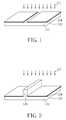
- a substrate 110is provided, wherein the substrate 110 is a bulk substrate, for example.
- a mask layer(not shown) is formed on the substrate, wherein the mask layer includes a pad oxide layer (not shown) and a nitride layer (not shown) located on the pad oxide layer.
- a photolithography process E 1is performed to pattern the mask layer for forming a patterned pad oxide layer 122 and a patterned nitride layer 124 and exposing a part of the substrate 110 . As shown in FIG.
- an epitaxial process E 2is performed to form a fin-shaped structure 120 on the exposed part of the substrate 110 , wherein the fin-shaped structure 120 protrudes from the pad oxide layer 122 and the nitride layer 124 .
- a photolithography processcan be performed on the substrate 110 by using the mask layer already patterned as a hard mask, so that desired fin-shaped structures can be formed from the part of the substrate 110 that is not etched. As shown in FIG. 3 , the patterned pad oxide layer 122 and the patterned nitride layer 124 are removed.
- An oxide layer 130is formed on the substrate 110 without the fin-shaped structure 120 being formed thereon, wherein the oxide layer 130 may be formed by processes such as a depositing process and an etching back process, for use as a shallow trench isolation structure. In another embodiment, the oxide layer 130 may also be an isolation structure. By doing this, a fin-shaped structure 120 can be formed on the substrate 110 , and an oxide layer 130 can be formed on the substrate 110 without the fin-shaped structure 120 being formed thereon.
- FIGS. 4-5schematically depict another forming method of this embodiment.
- a silicon-on-insulator substrate 210is provided, which includes a silicon substrate 212 , a bottom oxide layer 214 located on the silicon substrate 212 and a silicon layer 216 located on the bottom oxide layer 214 .
- the silicon layer 216is patterned to form the fin-shaped structures 220 and a part of the bottom oxide layer 214 without exposing the fin-shaped structure 220 formed thereon.
- the fin-shaped structure 220can also be formed on the silicon substrate 212 , and an oxide layer (such as the bottom oxide layer 214 ) can be formed on the silicon substrate 212 without the fin-shaped structure 220 being formed thereon.
- an oxide layersuch as the bottom oxide layer 214
- FIG. 3 and FIG. 5The difference between FIG. 3 and FIG. 5 is: the oxide layer 130 formed on the silicon substrate 110 is just located on the substrate 110 without the fin-shaped structure 120 being formed thereon (as shown in FIG. 3 ), but the bottom oxide layer 214 formed in the silicon-on-insulator substrate 210 has the fin-shaped structure 220 located thereon.
- This embodimentdepicts a single fin-shaped structure 120 or 220 to illustrate the semiconductor process of the present invention, but the semiconductor process of the present invention can also be applied to a substrate having a plurality of fin-shaped structures.
- a gate 140is formed to cover a part of the oxide layer 130 and a part of the fin-shaped structure 120 .
- the forming method of the gate 140may include: forming a gate dielectric layer 142 covering a part of the oxide layer 130 and a part of the fin-shaped structure 120 ; forming a gate electrode layer 144 covering the gate dielectric layer 142 ; forming a cap layer 146 covering the gate electrode layer 144 ; patterning the cap layer 146 , the gate electrode layer 144 and the gate dielectric layer 142 ; and forming a spacer 148 beside the pattern gate dielectric layer 142 , gate electrode layer 144 and cap layer 146 .
- the material of the gate dielectric layer 142may include silicon dioxide, silicon nitride, silicon oxynitride, high-k dielectric material such as metallic oxide, etc.
- the material of the gate electrode layer 144may include heavily doped polysilicon, metallic oxide silicon, or metal alloys for forming a metal gate by a gate first process, such as metallic oxide silicon, titanium, tantalum, titanium nitride, tantalum nitride, or tungsten, etc.
- a replacement metal gate (RMG) processsuch as a gate-last process, can be performed to replace the polysilicon electrode layer with the metal electrode layer.
- the cap layer 146 and the spacer 148may be composed of silicon nitride.
- the spacer 148may be a multilayer structure (not shown) including the inner spacer and an outer spacer.
- the forming methods of the gate 140are known in the art, and not described herein.
- an etching process E 3is performed to etch a part of the fin-shaped structure 120 beside the gate 140 , so that a recess R in the fin-shaped structure 120 is formed on either side of the gate 140 respectively.
- the etching process E 3may include a dry etching process or a wet etching process.
- the etching process E 3may include a dry etching process and a wet etching process, or at least one wet etching process.
- the wet etching processcomprises etching by an etchant containing ammonia, hydrogen peroxide and water, which performs at least an etching process to form the recess R using the characteristic of different etching rates applied to various crystal planes of the fin-shaped structure 120 .
- the desired shape of the recess Rcan be attained by adjusting the ratio of ammonia, hydrogen peroxide and water in the etchant.
- the recess Rmay be obtained by performing a wet etching process one or more times using different etchants, wherein the etchants may be ammonia etchant, methyl ammonium hydroxide etchant, hydroxide etchant, or ethylene diamine pyrocatechol etchant, etc. Therefore, the present invention can form the recess R having a hexagon-shaped profile structure.
- FIG. 9schematically depicts a cross-sectional view of a semiconductor process along line A-A′ and above the plane S of FIG. 7 .
- the recess R located in a part of the fin-shaped structure 120 beside the gate 140is formed by the etching process E 3 , wherein the recess R has a hexagon-shaped profile structure.
- a part of the fin-shaped structure 120will be reserved below the recess R for forming an epitaxial layer in the recess R by a later epitaxial process.
- an epitaxial process E 4is performed to form an epitaxial layer 150 having a hexagon-shaped profile structure in the recess R.
- the epitaxial layer 150may include a silicon-germanium epitaxial layer suited for a PMOS transistor, or a silicon-carbide epitaxial layer suited for an NMOS transistor, depending upon the electrical properties of the Multi-gate MOSFET.
- FIG. 10schematically depicts a cross-sectional view of a semiconductor process along line A-A′ and above the plane S of FIG. 8 .
- the epitaxial layer 150is formed in the recess R, and grows conformally along the shape of the recess R, therefore having a hexagon-shaped profile structure.
- the level of the top surface S 1 of the epitaxial layer 150is higher than the level of the top surface S 2 of the fin-shaped structure 120 .
- an ion implantation processmay be performed to dope impurities, or impurities may be doped while performing the epitaxial process E 4 , so that the epitaxial layer 150 can be used as a source/drain region.
- a silicide process(or a salicide process, not shown) may be performed to form silicide in the source/drain region, wherein the silicide process may include a post clean process, a metal depositing process, an annealing process, a selective etching process, or a test process, etc. Thereafter, other processes may be performed after the silicide process is performed.
- the present inventionprovides a semiconductor process that etches and forms at least a recess having a specific profile structure in the fin-shaped structure beside the gate, wherein the etching methods may include a dry etching process or a wet etching process.
- the wet etching processcomprises etching by an etchant containing ammonia, hydrogen peroxide and water.
- the epitaxial layer formed in the recess Rhas a hexagon-shaped profile structure and therefore improves performance of the semiconductor structure. For instance, after the epitaxial layer is formed, the spacer can be removed more easily.
- the epitaxial layer formed in the present inventionmakes it easier to force stress to the gate channel below the gate structure and enhance the carrier mobility of the gate channel.
Landscapes
- Insulated Gate Type Field-Effect Transistor (AREA)
Abstract
Description
1. Field of the Invention
The present invention relates generally to a semiconductor process, and more specifically, to a semiconductor process that forms at least a recess in a fin-shaped structure beside a gate structure, thereby forming an epitaxial layer having a hexagon-shaped profile structure in the recess.
2. Description of the Prior Art
With increasing miniaturization of semiconductor devices, various Fin-shaped field effect transistor (FinFET) devices have been developed. The Fin-shaped field effect transistor (FinFET) is advantageous for the following reasons. First, manufacturing processes of Fin-shaped field effect transistor (FinFET) devices can be integrated into traditional logic device processes, and thus are more compatible. In addition, since the three-dimensional structure of the FinFET increases the overlapping area between the gate and the substrate, the channel region is controlled more effectively. This therefore reduces drain-induced barrier lowering (DIBL) effect and short channel effect. Moreover, the channel region is longer for the same gate length. Therefore, the current between the source and the drain is increased.
In a current FinFET process, agate structure (which may include a gate dielectric layer, a gate electrode located on the gate dielectric layer, a cap layer located on the gate electrode, and a spacer located beside the gate dielectric layer, the gate electrode and the cap layer) is formed on a substrate having at least a fin-shaped structure. Then, epitaxial layers are formed on the fin-shaped structure beside the gate structure. Thereafter, other processes such as removing spacers of the gate structure may be performed.
However, the epitaxial layers make removal of the spacers difficult. The distance between the epitaxial layers on either side of the gate structure is also too great, resulting in insufficient stress forcing the gate channel below the gate structure, and limited ability to enhance carrier mobility of the gate channel through the epitaxial layers.
Therefore, a semiconductor process, more specifically a FinFET process, which can improve the performance of the epitaxial layers is needed in the industry.
The present invention provides a semiconductor process, that can etch and form at least a recess in a fin-shaped structure beside a gate structure, so that form an epitaxial layer having a hexagon-shaped profile structure in the recess, therefore a Multi-gate MOSFET such as a FinFET or a Tri-gate MOSFET can be formed.
The present invention provides a semiconductor process including the following steps. A substrate is provided. At least a fin-shaped structure is formed on the substrate. An oxide layer is formed on the substrate without the fin-shaped structure being formed thereon. A gate covering a part of the oxide layer and a part of the fin-shaped structure is formed. An etching process is performed to etch a part of the fin-shaped structure beside the gate, therefore forming at least a recess in the fin-shaped structure. An epitaxial process is performed to form an epitaxial layer in the recess, wherein the epitaxial layer has a hexagon-shaped profile structure.
The present invention provides a semiconductor process, that etches at least a recess having a specific profile structure in the fin-shaped structure beside the gate structure. Thus, an epitaxial layer having a hexagon-shaped profile structure can be formed in the recess, and the performance of the semiconductor structure can therefore be improved. For example, the epitaxial layer formed in the present invention can make spacers easier to be removed. Besides, the epitaxial layer formed in the present invention can be easier to force stresses to the gate channel below the gate structure, so that improving the carrier mobility in the gate channel.
These and other objectives of the present invention will no doubt become obvious to those of ordinary skill in the art after reading the following detailed description of the preferred embodiment that is illustrated in the various figures and drawings.
Please refer toFIGS. 1-3 . As shown inFIG. 1 , asubstrate 110 is provided, wherein thesubstrate 110 is a bulk substrate, for example. A mask layer (not shown) is formed on the substrate, wherein the mask layer includes a pad oxide layer (not shown) and a nitride layer (not shown) located on the pad oxide layer. A photolithography process E1 is performed to pattern the mask layer for forming a patternedpad oxide layer 122 and a patternednitride layer 124 and exposing a part of thesubstrate 110. As shown inFIG. 2 , an epitaxial process E2 is performed to form a fin-shaped structure 120 on the exposed part of thesubstrate 110, wherein the fin-shaped structure 120 protrudes from thepad oxide layer 122 and thenitride layer 124. In addition, a photolithography process can be performed on thesubstrate 110 by using the mask layer already patterned as a hard mask, so that desired fin-shaped structures can be formed from the part of thesubstrate 110 that is not etched. As shown inFIG. 3 , the patternedpad oxide layer 122 and the patternednitride layer 124 are removed. Anoxide layer 130 is formed on thesubstrate 110 without the fin-shaped structure 120 being formed thereon, wherein theoxide layer 130 may be formed by processes such as a depositing process and an etching back process, for use as a shallow trench isolation structure. In another embodiment, theoxide layer 130 may also be an isolation structure. By doing this, a fin-shaped structure 120 can be formed on thesubstrate 110, and anoxide layer 130 can be formed on thesubstrate 110 without the fin-shaped structure 120 being formed thereon.
Additionally, please refer toFIGS. 4-5 , which schematically depict another forming method of this embodiment. As shown inFIG. 4 , a silicon-on-insulator substrate 210 is provided, which includes asilicon substrate 212, abottom oxide layer 214 located on thesilicon substrate 212 and asilicon layer 216 located on thebottom oxide layer 214. As shown inFIG. 5 , thesilicon layer 216 is patterned to form the fin-shaped structures220 and a part of thebottom oxide layer 214 without exposing the fin-shaped structure220 formed thereon. In this way, the fin-shaped structure220 can also be formed on thesilicon substrate 212, and an oxide layer (such as the bottom oxide layer214) can be formed on thesilicon substrate 212 without the fin-shaped structure220 being formed thereon. The difference betweenFIG. 3 andFIG. 5 is: theoxide layer 130 formed on thesilicon substrate 110 is just located on thesubstrate 110 without the fin-shaped structure 120 being formed thereon (as shown inFIG. 3 ), but thebottom oxide layer 214 formed in the silicon-on-insulator substrate 210 has the fin-shaped structure220 located thereon. However, the difference does not affect later semiconductor processes of the present invention. This embodiment depicts a single fin-shaped structure 120 or220 to illustrate the semiconductor process of the present invention, but the semiconductor process of the present invention can also be applied to a substrate having a plurality of fin-shaped structures.
As shown inFIG. 6 , agate 140 is formed to cover a part of theoxide layer 130 and a part of the fin-shaped structure 120. The forming method of thegate 140 may include: forming a gatedielectric layer 142 covering a part of theoxide layer 130 and a part of the fin-shaped structure 120; forming agate electrode layer 144 covering the gatedielectric layer 142; forming acap layer 146 covering thegate electrode layer 144; patterning thecap layer 146, thegate electrode layer 144 and the gatedielectric layer 142; and forming aspacer 148 beside the pattern gatedielectric layer 142,gate electrode layer 144 andcap layer 146. In one embodiment, the material of the gatedielectric layer 142 may include silicon dioxide, silicon nitride, silicon oxynitride, high-k dielectric material such as metallic oxide, etc. The material of thegate electrode layer 144 may include heavily doped polysilicon, metallic oxide silicon, or metal alloys for forming a metal gate by a gate first process, such as metallic oxide silicon, titanium, tantalum, titanium nitride, tantalum nitride, or tungsten, etc. In one case, if thegate electrode layer 144 of thegate structure 140 is a polysilicon electrode layer, a replacement metal gate (RMG) process, such as a gate-last process, can be performed to replace the polysilicon electrode layer with the metal electrode layer. Thecap layer 146 and thespacer 148 may be composed of silicon nitride. Thespacer 148 may be a multilayer structure (not shown) including the inner spacer and an outer spacer. The forming methods of thegate 140 are known in the art, and not described herein.
As shown inFIG. 7 , an etching process E3 is performed to etch a part of the fin-shapedstructure 120 beside thegate 140, so that a recess R in the fin-shapedstructure 120 is formed on either side of thegate 140 respectively. In the present invention, the etching process E3 may include a dry etching process or a wet etching process. In a preferred embodiment, the etching process E3 may include a dry etching process and a wet etching process, or at least one wet etching process. In one case, the wet etching process comprises etching by an etchant containing ammonia, hydrogen peroxide and water, which performs at least an etching process to form the recess R using the characteristic of different etching rates applied to various crystal planes of the fin-shapedstructure 120. Furthermore, the desired shape of the recess R can be attained by adjusting the ratio of ammonia, hydrogen peroxide and water in the etchant. In another embodiment, the recess R may be obtained by performing a wet etching process one or more times using different etchants, wherein the etchants may be ammonia etchant, methyl ammonium hydroxide etchant, hydroxide etchant, or ethylene diamine pyrocatechol etchant, etc. Therefore, the present invention can form the recess R having a hexagon-shaped profile structure.
In this embodiment, the recess R formed by the etching process will pass through the short axis X of the fin-shapedstructure 120, but will not pass through the long axis y of the fin-shapedstructure 120, therefore a source/drain region can be formed in the recess R.FIG. 9 schematically depicts a cross-sectional view of a semiconductor process along line A-A′ and above the plane S ofFIG. 7 . As shown inFIG. 9 , the recess R located in a part of the fin-shapedstructure 120 beside thegate 140 is formed by the etching process E3, wherein the recess R has a hexagon-shaped profile structure. In this embodiment, a part of the fin-shapedstructure 120 will be reserved below the recess R for forming an epitaxial layer in the recess R by a later epitaxial process.
As shown inFIG. 8 , an epitaxial process E4 is performed to form anepitaxial layer 150 having a hexagon-shaped profile structure in the recess R. Theepitaxial layer 150 may include a silicon-germanium epitaxial layer suited for a PMOS transistor, or a silicon-carbide epitaxial layer suited for an NMOS transistor, depending upon the electrical properties of the Multi-gate MOSFET.FIG. 10 schematically depicts a cross-sectional view of a semiconductor process along line A-A′ and above the plane S ofFIG. 8 . Theepitaxial layer 150 is formed in the recess R, and grows conformally along the shape of the recess R, therefore having a hexagon-shaped profile structure. In a preferred embodiment, the level of the top surface S1 of theepitaxial layer 150 is higher than the level of the top surface S2 of the fin-shapedstructure 120.
Thereafter, an ion implantation process may be performed to dope impurities, or impurities may be doped while performing the epitaxial process E4, so that theepitaxial layer 150 can be used as a source/drain region. After theepitaxial layer 150 is formed, a silicide process (or a salicide process, not shown) may be performed to form silicide in the source/drain region, wherein the silicide process may include a post clean process, a metal depositing process, an annealing process, a selective etching process, or a test process, etc. Thereafter, other processes may be performed after the silicide process is performed.
Above all, the present invention provides a semiconductor process that etches and forms at least a recess having a specific profile structure in the fin-shaped structure beside the gate, wherein the etching methods may include a dry etching process or a wet etching process. Preferably, the wet etching process comprises etching by an etchant containing ammonia, hydrogen peroxide and water. The epitaxial layer formed in the recess R has a hexagon-shaped profile structure and therefore improves performance of the semiconductor structure. For instance, after the epitaxial layer is formed, the spacer can be removed more easily. The epitaxial layer formed in the present invention makes it easier to force stress to the gate channel below the gate structure and enhance the carrier mobility of the gate channel.
Those skilled in the art will readily observe that numerous modifications and alterations of the device and method may be made while retaining the teachings of the invention. Accordingly, the above disclosure should be construed as limited only by the metes and bounds of the appended claims.
Claims (13)
1. A semiconductor process, comprising:
providing a substrate;
forming at least a fin-shaped structure on the substrate;
forming an oxide layer on the substrate without the fin-shaped structure being formed thereon;
forming a gate covering a part of the oxide layer and a part of the fin-shaped structure;
performing an etching process to etch a part of the fin-shaped structure beside the gate to form at least a hexagon-shaped recess in the fin-shaped structure; and
performing an epitaxial process to form an epitaxial layer in the hexagon-shaped recess, wherein the epitaxial layer has a hexagon-shaped profile structure.
2. The semiconductor process according toclaim 1 , wherein the substrate comprises a bulk substrate or a silicon-on-insulator substrate.
3. The semiconductor process according toclaim 2 , wherein the steps of forming the fin-shaped structure comprise:
forming a mask layer on the bulk substrate;
performing a photolithography process to pattern the mask layer and expose a part of the bulk substrate; and
performing an epitaxial process to form the fin-shaped structure on the exposed part of the bulk substrate.
4. The semiconductor process according toclaim 3 , wherein the mask layer comprises a pad oxide layer and a nitride layer.
5. The semiconductor process according toclaim 2 , wherein the silicon-on-insulator substrate comprises:
a silicon substrate;
a bottom oxide layer located on the silicon substrate; and
a silicon layer located on the bottom oxide layer.
6. The semiconductor process according toclaim 5 , wherein the steps of forming the fin-shaped structure on the silicon-on-insulator substrate and forming the oxide layer on the substrate without the fin-shaped structure being formed thereon comprise:
patterning the silicon layer to form the fin-shaped structure, and exposing a part of the bottom oxide layer on the substrate without the fin-shaped structure being formed thereon.
7. The semiconductor process according toclaim 1 , wherein forming the gate comprises:
forming a gate dielectric layer covering the oxide layer and the fin-shaped structure;
forming a gate electrode layer covering the gate dielectric layer;
forming a cap layer covering the gate electrode layer;
patterning the cap layer, the gate electrode layer and the gate dielectric layer; and
forming a spacer beside the patterned gate dielectric layer, gate electrode layer and cap layer.
8. The semiconductor process according toclaim 7 , wherein the gate electrode layer comprises a polysilicon electrode layer.
9. The semiconductor process according toclaim 8 , further comprising:
performing a replacement metal gate (RMG) process to replace the polysilicon electrode layer with a metal electrode layer.
10. The semiconductor process according toclaim 1 , wherein the etching process comprises a dry etching process or a wet etching process.
11. The semiconductor process according toclaim 10 , wherein the etching process comprises a dry etching process and a wet etching process.
12. The semiconductor process according toclaim 10 , wherein the wet etching process comprises etching by an etchant containing ammonia, hydrogen peroxide and water.
13. The semiconductor process according toclaim 1 , wherein the epitaxial process comprises a silicon-germanium epitaxial layer or a silicon-carbide epitaxial layer.
Priority Applications (1)
| Application Number | Priority Date | Filing Date | Title |
|---|---|---|---|
| US13/216,259US8674433B2 (en) | 2011-08-24 | 2011-08-24 | Semiconductor process |
Applications Claiming Priority (1)
| Application Number | Priority Date | Filing Date | Title |
|---|---|---|---|
| US13/216,259US8674433B2 (en) | 2011-08-24 | 2011-08-24 | Semiconductor process |
Publications (2)
| Publication Number | Publication Date |
|---|---|
| US20130052778A1 US20130052778A1 (en) | 2013-02-28 |
| US8674433B2true US8674433B2 (en) | 2014-03-18 |
Family
ID=47744284
Family Applications (1)
| Application Number | Title | Priority Date | Filing Date |
|---|---|---|---|
| US13/216,259Active2032-01-18US8674433B2 (en) | 2011-08-24 | 2011-08-24 | Semiconductor process |
Country Status (1)
| Country | Link |
|---|---|
| US (1) | US8674433B2 (en) |
Cited By (3)
| Publication number | Priority date | Publication date | Assignee | Title |
|---|---|---|---|---|
| US9024368B1 (en)* | 2013-11-14 | 2015-05-05 | Globalfoundries Inc. | Fin-type transistor structures with extended embedded stress elements and fabrication methods |
| US9941174B2 (en) | 2015-03-20 | 2018-04-10 | Samsung Electronics Co., Ltd. | Semiconductor devices having fin active regions |
| US10790378B2 (en)* | 2017-11-30 | 2020-09-29 | Intel Corporation | Replacement gate structures for advanced integrated circuit structure fabrication |
Families Citing this family (15)
| Publication number | Priority date | Publication date | Assignee | Title |
|---|---|---|---|---|
| US8912606B2 (en)* | 2012-04-24 | 2014-12-16 | Globalfoundries Inc. | Integrated circuits having protruding source and drain regions and methods for forming integrated circuits |
| US20140167163A1 (en)* | 2012-12-17 | 2014-06-19 | International Business Machines Corporation | Multi-Fin FinFETs with Epitaxially-Grown Merged Source/Drains |
| US20140264607A1 (en)* | 2013-03-13 | 2014-09-18 | International Business Machines Corporation | Iii-v finfets on silicon substrate |
| KR102017625B1 (en)* | 2013-05-10 | 2019-10-22 | 삼성전자주식회사 | Semiconductor device and method of manufacturing the same |
| CN103346086B (en)* | 2013-05-31 | 2016-08-10 | 上海华力微电子有限公司 | The manufacture method of embedded germanium silicon structure |
| US9070710B2 (en) | 2013-06-07 | 2015-06-30 | United Microelectronics Corp. | Semiconductor process |
| CN104241360B (en)* | 2013-06-24 | 2019-07-23 | 联华电子股份有限公司 | Semiconductor device and method for fabricating the same |
| KR102073967B1 (en)* | 2013-07-30 | 2020-03-02 | 삼성전자주식회사 | Semiconductor device including field effect transistor |
| KR102072410B1 (en) | 2013-08-07 | 2020-02-03 | 삼성전자 주식회사 | Semiconductor device and fabricated method thereof |
| CN103476229A (en)* | 2013-09-16 | 2013-12-25 | 南京九致信息科技有限公司 | Heat radiating device |
| EP3123521A4 (en) | 2014-03-27 | 2017-10-25 | Intel Corporation | Confined epitaxial regions for semiconductor devices and methods of fabricating semiconductor devices having confined epitaxial regions |
| KR102200345B1 (en) | 2014-06-26 | 2021-01-11 | 삼성전자주식회사 | Semiconductor device and method of manufacturing the same |
| US9202919B1 (en)* | 2014-07-31 | 2015-12-01 | Stmicroelectronics, Inc. | FinFETs and techniques for controlling source and drain junction profiles in finFETs |
| US9306001B1 (en) | 2015-04-14 | 2016-04-05 | International Business Machines Corporation | Uniformly doped leakage current stopper to counter under channel leakage currents in bulk FinFET devices |
| CN106549053B (en)* | 2015-09-17 | 2021-07-27 | 联华电子股份有限公司 | Semiconductor structure and method of making the same |
Citations (162)
| Publication number | Priority date | Publication date | Assignee | Title |
|---|---|---|---|---|
| US4891303A (en) | 1988-05-26 | 1990-01-02 | Texas Instruments Incorporated | Trilayer microlithographic process using a silicon-based resist as the middle layer |
| US5217910A (en) | 1990-11-05 | 1993-06-08 | Mitsubishi Denki Kabushiki Kaisha | Method of fabricating semiconductor device having sidewall spacers and oblique implantation |
| US5273930A (en) | 1992-09-03 | 1993-12-28 | Motorola, Inc. | Method of forming a non-selective silicon-germanium epitaxial film |
| US5356830A (en) | 1988-09-19 | 1994-10-18 | Kabushiki Kaisha Tobshiba | Semiconductor device and its manufacturing method |
| US5372957A (en) | 1993-07-22 | 1994-12-13 | Taiwan Semiconductor Manufacturing Company | Multiple tilted angle ion implantation MOSFET method |
| US5385630A (en) | 1993-06-29 | 1995-01-31 | Digital Equipment Corporation | Process for increasing sacrificial oxide etch rate to reduce field oxide loss |
| US5399506A (en) | 1992-08-13 | 1995-03-21 | Sony Corporation | Semiconductor fabricating process |
| US5625217A (en) | 1992-12-11 | 1997-04-29 | Intel Corporation | MOS transistor having a composite gate electrode and method of fabrication |
| US5777364A (en) | 1992-11-30 | 1998-07-07 | International Business Machines Corporation | Graded channel field effect transistor |
| US5783479A (en) | 1997-06-23 | 1998-07-21 | National Science Council | Structure and method for manufacturing improved FETs having T-shaped gates |
| US5960322A (en) | 1997-12-19 | 1999-09-28 | Advanced Micro Devices, Inc. | Suppression of boron segregation for shallow source and drain junctions in semiconductors |
| US6030874A (en) | 1997-01-21 | 2000-02-29 | Texas Instruments Incorporated | Doped polysilicon to retard boron diffusion into and through thin gate dielectrics |
| US6043138A (en) | 1996-09-16 | 2000-03-28 | Advanced Micro Devices, Inc. | Multi-step polysilicon deposition process for boron penetration inhibition |
| US6048756A (en) | 1997-07-31 | 2000-04-11 | Electronics And Telecommunications Research Institute | Method for making a silicon-on-insulator MOS transistor using a selective SiGe epitaxy |
| US6074954A (en) | 1998-08-31 | 2000-06-13 | Applied Materials, Inc | Process for control of the shape of the etch front in the etching of polysilicon |
| US6100171A (en) | 1998-03-03 | 2000-08-08 | Advanced Micro Devices, Inc. | Reduction of boron penetration by laser anneal removal of fluorine |
| US6110787A (en) | 1999-09-07 | 2000-08-29 | Chartered Semiconductor Manufacturing Ltd. | Method for fabricating a MOS device |
| US6165826A (en) | 1994-12-23 | 2000-12-26 | Intel Corporation | Transistor with low resistance tip and method of fabrication in a CMOS process |
| US6165881A (en) | 1998-10-23 | 2000-12-26 | Taiwan Semiconductor Manufacturing Company | Method of forming salicide poly gate with thin gate oxide and ultra narrow gate width |
| US6191052B1 (en) | 1999-01-25 | 2001-02-20 | Taiwan Semiconductor Manufacturing Company | Method for fabricating an ultra-shallow junction with low resistance using a screen oxide formed by poly re-oxidation in a nitrogen containing atmosphere |
| US6228730B1 (en) | 1999-04-28 | 2001-05-08 | United Microelectronics Corp. | Method of fabricating field effect transistor |
| US6274447B1 (en) | 1996-03-22 | 2001-08-14 | Seiko Epson Corporation | Semiconductor device comprising a MOS element and a fabrication method thereof |
| US20020011612A1 (en)* | 2000-07-31 | 2002-01-31 | Kabushiki Kaisha Toshiba | Semiconductor device and method for manufacturing the same |
| US6355533B2 (en) | 1999-12-24 | 2002-03-12 | Hyundai Electronics Industries Co., Ltd. | Method for manufacturing semiconductor device |
| US6365476B1 (en) | 2000-10-27 | 2002-04-02 | Ultratech Stepper, Inc. | Laser thermal process for fabricating field-effect transistors |
| US6368926B1 (en) | 2000-03-13 | 2002-04-09 | Advanced Micro Devices, Inc. | Method of forming a semiconductor device with source/drain regions having a deep vertical junction |
| US6444591B1 (en) | 2000-09-30 | 2002-09-03 | Newport Fab, Llc | Method for reducing contamination prior to epitaxial growth and related structure |
| US20020160587A1 (en) | 2001-04-30 | 2002-10-31 | Basanth Jagannathan | Method to increase carbon and boron doping concentrations in Si and SiGe films |
| US20020182423A1 (en) | 2001-04-20 | 2002-12-05 | International Business Machines Corporation | Epitaxial and polycrystalline growth of Si1-x-yGexCy and Si1-yCy alloy layers on Si by UHV-CVD |
| US6492216B1 (en) | 2002-02-07 | 2002-12-10 | Taiwan Semiconductor Manufacturing Company | Method of forming a transistor with a strained channel |
| US6537370B1 (en) | 1998-09-10 | 2003-03-25 | FRANCE TéLéCOM | Process for obtaining a layer of single-crystal germanium on a substrate of single-crystal silicon, and products obtained |
| US6544822B2 (en) | 2000-06-21 | 2003-04-08 | Hynix Semiconductor, Inc. | Method for fabricating MOSFET device |
| US6605498B1 (en) | 2002-03-29 | 2003-08-12 | Intel Corporation | Semiconductor transistor having a backfilled channel material |
| US6613695B2 (en) | 2000-11-24 | 2003-09-02 | Asm America, Inc. | Surface preparation prior to deposition |
| US6621131B2 (en) | 2001-11-01 | 2003-09-16 | Intel Corporation | Semiconductor transistor having a stressed channel |
| US6624068B2 (en) | 2001-08-24 | 2003-09-23 | Texas Instruments Incorporated | Polysilicon processing using an anti-reflective dual layer hardmask for 193 nm lithography |
| US20030181005A1 (en) | 2002-03-19 | 2003-09-25 | Kiyota Hachimine | Semiconductor device and a method of manufacturing the same |
| US6632718B1 (en) | 1998-07-15 | 2003-10-14 | Texas Instruments Incorporated | Disposable spacer technology for reduced cost CMOS processing |
| US20030203599A1 (en) | 2000-03-27 | 2003-10-30 | Matsushita Electric Industrial Co. , Ltd. | Semiconductor wafer and method for fabricating the same |
| US6642122B1 (en) | 2002-09-26 | 2003-11-04 | Advanced Micro Devices, Inc. | Dual laser anneal for graded halo profile |
| US6664156B1 (en) | 2002-07-31 | 2003-12-16 | Chartered Semiconductor Manufacturing, Ltd | Method for forming L-shaped spacers with precise width control |
| US6676764B2 (en) | 2001-04-30 | 2004-01-13 | Hynix Semiconductor Inc. | Method for cleaning a substrate in selective epitaxial growth process |
| US6703271B2 (en) | 2001-11-30 | 2004-03-09 | Taiwan Semiconductor Manufacturing Company | Complementary metal oxide semiconductor transistor technology using selective epitaxy of a strained silicon germanium layer |
| US20040045499A1 (en) | 2002-06-10 | 2004-03-11 | Amberwave Systems Corporation | Source and drain elements |
| US20040067631A1 (en) | 2002-10-03 | 2004-04-08 | Haowen Bu | Reduction of seed layer roughness for use in forming SiGe gate electrode |
| US6777275B1 (en) | 2000-11-15 | 2004-08-17 | Advanced Micro Devices, Inc. | Single anneal for dopant activation and silicide formation |
| US20040195624A1 (en) | 2003-04-04 | 2004-10-07 | National Taiwan University | Strained silicon fin field effect transistor |
| US6806151B2 (en) | 2001-12-14 | 2004-10-19 | Texas Instruments Incorporated | Methods and apparatus for inducing stress in a semiconductor device |
| US6809402B1 (en) | 2002-08-14 | 2004-10-26 | Advanced Micro Devices, Inc. | Reflowable-doped HDP film |
| US20040227164A1 (en) | 2003-05-14 | 2004-11-18 | Samsung Electronics Co., Ltd. | MOS transistor with elevated source/drain structure and method of fabricating the same |
| US6858506B2 (en) | 2002-08-08 | 2005-02-22 | Macronix International Co., Ltd. | Method for fabricating locally strained channel |
| US6864135B2 (en) | 2002-10-31 | 2005-03-08 | Freescale Semiconductor, Inc. | Semiconductor fabrication process using transistor spacers of differing widths |
| US20050051825A1 (en) | 2003-09-09 | 2005-03-10 | Makoto Fujiwara | Semiconductor device and manufacturing method thereof |
| US6869867B2 (en) | 1997-10-01 | 2005-03-22 | Kabushiki Kaisha Toshiba | Semiconductor device comprising metal silicide films formed to cover gate electrode and source-drain diffusion layers and method of manufacturing the same wherein the silicide on gate is thicker than on source-drain |
| US20050070076A1 (en) | 2001-10-26 | 2005-03-31 | Dion Michel Maurice | Method of depositing high-quality sige on sige substrates |
| US20050079692A1 (en) | 2003-10-10 | 2005-04-14 | Applied Materials, Inc. | Methods to fabricate MOSFET devices using selective deposition process |
| US20050082616A1 (en) | 2003-10-20 | 2005-04-21 | Huajie Chen | High performance stress-enhanced MOSFETs using Si:C and SiGe epitaxial source/drain and method of manufacture |
| US6887751B2 (en) | 2003-09-12 | 2005-05-03 | International Business Machines Corporation | MOSFET performance improvement using deformation in SOI structure |
| US6887762B1 (en) | 1998-11-12 | 2005-05-03 | Intel Corporation | Method of fabricating a field effect transistor structure with abrupt source/drain junctions |
| US6891192B2 (en) | 2003-08-04 | 2005-05-10 | International Business Machines Corporation | Structure and method of making strained semiconductor CMOS transistors having lattice-mismatched semiconductor regions underlying source and drain regions |
| US20050139231A1 (en) | 2003-12-31 | 2005-06-30 | Commissariat A L'energie Atomique | Method of wet cleaning a surface, especially of a material of the silicon-germanium type |
| US20050156171A1 (en)* | 2003-12-30 | 2005-07-21 | Brask Justin K. | Nonplanar transistors with metal gate electrodes |
| US6921963B2 (en) | 2003-01-23 | 2005-07-26 | Advanced Micro Devices, Inc | Narrow fin FinFET |
| US6930007B2 (en) | 2003-09-15 | 2005-08-16 | Texas Instruments Incorporated | Integration of pre-S/D anneal selective nitride/oxide composite cap for improving transistor performance |
| US6946350B2 (en) | 2003-12-31 | 2005-09-20 | Intel Corporation | Controlled faceting of source/drain regions |
| US6962856B2 (en) | 2002-07-19 | 2005-11-08 | Hynix Semiconductor, Inc. | Method for forming device isolation film of semiconductor device |
| US20050260830A1 (en) | 2004-03-25 | 2005-11-24 | Doo-Won Kwon | Methods of fabricating a semiconductor device using a dilute aqueous solution of an ammonia and peroxide mixture |
| US6972461B1 (en) | 2004-06-30 | 2005-12-06 | International Business Machines Corporation | Channel MOSFET with strained silicon channel on strained SiGe |
| US20050285193A1 (en) | 2004-06-28 | 2005-12-29 | Lee Sung-Young | Semiconductor device and method of manufacturing same |
| US20050287752A1 (en) | 2004-06-24 | 2005-12-29 | Applied Materials, Inc. | Methods for forming a transistor |
| US6991979B2 (en) | 2003-09-22 | 2006-01-31 | International Business Machines Corporation | Method for avoiding oxide undercut during pre-silicide clean for thin spacer FETs |
| US6991991B2 (en) | 2003-11-12 | 2006-01-31 | United Microelectronics Corp. | Method for preventing to form a spacer undercut in SEG pre-clean process |
| US20060051922A1 (en) | 2004-09-09 | 2006-03-09 | Taiwan Semiconductor Manufacturing Company, Ltd. | Strained silicon device manufacturing method |
| US20060057859A1 (en) | 2004-09-16 | 2006-03-16 | International Business Machines Corporation | Buffer layer for selective SiGe growth for uniform nucleation |
| US20060076627A1 (en) | 2004-10-12 | 2006-04-13 | International Business Machines Corporation | Ultra shallow junction formation by epitaxial interface limited diffusion |
| US20060088968A1 (en) | 2004-06-17 | 2006-04-27 | Samsung Electronics Co., Ltd. | Methods of fabricating a semiconductor device using a selective epitaxial growth technique |
| US7037773B2 (en) | 2004-03-29 | 2006-05-02 | United Microelectronics Corp. | Method of manufacturing metal-oxide-semiconductor transistor |
| US20060099830A1 (en) | 2004-11-05 | 2006-05-11 | Varian Semiconductor Equipment Associates, Inc. | Plasma implantation using halogenated dopant species to limit deposition of surface layers |
| US20060115949A1 (en) | 2004-12-01 | 2006-06-01 | Freescale Semiconductor, Inc. | Semiconductor fabrication process including source/drain recessing and filling |
| US7060576B2 (en) | 2003-10-24 | 2006-06-13 | Intel Corporation | Epitaxially deposited source/drain |
| US7060579B2 (en) | 2004-07-29 | 2006-06-13 | Texas Instruments Incorporated | Increased drive current by isotropic recess etch |
| US7087477B2 (en) | 2001-12-04 | 2006-08-08 | International Business Machines Corporation | FinFET SRAM cell using low mobility plane for cell stability and method for forming |
| US7091551B1 (en) | 2005-04-13 | 2006-08-15 | International Business Machines Corporation | Four-bit FinFET NVRAM memory device |
| US7112495B2 (en) | 2003-08-15 | 2006-09-26 | Taiwan Semiconductor Manufacturing Company, Ltd. | Structure and method of a strained channel transistor and a second semiconductor component in an integrated circuit |
| US7118952B2 (en) | 2004-07-14 | 2006-10-10 | Taiwan Semiconductor Manufacturing Co., Ltd. | Method of making transistor with strained source/drain |
| US20060228842A1 (en) | 2005-04-07 | 2006-10-12 | Freescale Semiconductor, Inc. | Transistor fabrication using double etch/refill process |
| US20060231826A1 (en) | 2005-04-18 | 2006-10-19 | Toshiba America Electronic Components, Inc. | Step-embedded SiGe structure for PFET mobility enhancement |
| US20060258126A1 (en) | 2003-02-04 | 2006-11-16 | Sumco Corporation | Semiconductor substrate, field-effect transistor, and their production methods |
| US20060281288A1 (en) | 2005-06-13 | 2006-12-14 | Fujitsu Limited | Semiconductor device fabrication method |
| US20060286729A1 (en) | 2005-06-21 | 2006-12-21 | Jack Kavalieros | Complementary metal oxide semiconductor integrated circuit using raised source drain and replacement metal gate |
| US20060292779A1 (en) | 2004-09-29 | 2006-12-28 | International Business Machines Corporation | Structure and method for making strained channel field effect transistor using sacrificial spacer |
| US20060292783A1 (en) | 2005-02-28 | 2006-12-28 | Young-Eun Lee | CMOS transistor and method of manufacturing the same |
| US7169675B2 (en) | 2004-07-07 | 2007-01-30 | Chartered Semiconductor Manufacturing, Ltd | Material architecture for the fabrication of low temperature transistor |
| US20070023847A1 (en) | 2005-07-26 | 2007-02-01 | Samsung Electronics Co., Ltd. | Semiconductor device and method of manufacturing the same |
| US20070034906A1 (en) | 2005-08-10 | 2007-02-15 | Taiwan Semiconductor Manufacturing Company, Ltd. | MOS devices with reduced recess on substrate surface |
| US7183596B2 (en) | 2005-06-22 | 2007-02-27 | Taiwan Semiconductor Manufacturing Company, Ltd. | Composite gate structure in an integrated circuit |
| US20070049014A1 (en) | 2005-08-25 | 2007-03-01 | Ming-Tsung Chen | Method of performing salicide processes on MOS transistors |
| US20070072376A1 (en) | 2005-09-29 | 2007-03-29 | Semiconductor Manufacturing International (Shanghai) Corporation | Strained-induced mobility enhancement nano-device structure and integrated process architecture for CMOS technologies |
| US20070072353A1 (en) | 2005-09-23 | 2007-03-29 | Chih-Ning Wu | Method of fabricating strained-silicon transistors and strained-silicon CMOS transistors |
| US7202124B2 (en) | 2004-10-01 | 2007-04-10 | Massachusetts Institute Of Technology | Strained gettering layers for semiconductor processes |
| US7217627B2 (en) | 2003-09-18 | 2007-05-15 | Dongbu Electronics Co., Ltd. | Semiconductor devices having diffusion barrier regions and halo implant regions and methods of fabricating the same |
| US20070108528A1 (en) | 2005-11-15 | 2007-05-17 | International Business Machines Corporation | Sram cell |
| US20070128783A1 (en) | 2005-12-06 | 2007-06-07 | Shyh-Fann Ting | Method for fabricating strained-silicon cmos transistors |
| US20070158756A1 (en) | 2006-01-12 | 2007-07-12 | Lars Dreeskornfeld | Production method for a FinFET transistor arrangement, and corresponding FinFET transistor arrangement |
| US20070166929A1 (en) | 2006-01-18 | 2007-07-19 | Sumco Corporation | Method of producing semiconductor wafer |
| US7247887B2 (en) | 2005-07-01 | 2007-07-24 | Synopsys, Inc. | Segmented channel MOS transistor |
| US7250658B2 (en) | 2003-06-26 | 2007-07-31 | International Business Machines Corporation | Hybrid planar and FinFET CMOS devices |
| US7288822B1 (en) | 2006-04-07 | 2007-10-30 | United Microelectronics Corp. | Semiconductor structure and fabricating method thereof |
| US20070262396A1 (en) | 2006-04-25 | 2007-11-15 | International Business Machines Corporation | Transistors Having V-shape Source/Drain Metal Contacts |
| US7303999B1 (en) | 2005-12-13 | 2007-12-04 | Lam Research Corporation | Multi-step method for etching strain gate recesses |
| US7309626B2 (en) | 2005-11-15 | 2007-12-18 | International Business Machines Corporation | Quasi self-aligned source/drain FinFET process |
| US20080014688A1 (en) | 2006-07-06 | 2008-01-17 | Voon-Yew Thean | Selective uniaxial stress modification for use with strained silicon on insulator integrated circuit |
| US7335959B2 (en) | 2005-01-06 | 2008-02-26 | Intel Corporation | Device with stepped source/drain region profile |
| US20080061366A1 (en) | 2006-09-11 | 2008-03-13 | United Microelectronics Corp. | Complementary metal-oxide-semiconductor device and fabricating method thereof |
| US20080067545A1 (en) | 2006-09-20 | 2008-03-20 | Samsung Electronics Co., Ltd | Semiconductor device including field effect transistor and method of forming the same |
| US20080076236A1 (en) | 2006-09-21 | 2008-03-27 | Jih-Shun Chiang | Method for forming silicon-germanium epitaxial layer |
| US7352034B2 (en) | 2005-08-25 | 2008-04-01 | International Business Machines Corporation | Semiconductor structures integrating damascene-body FinFET's and planar devices on a common substrate and methods for forming such semiconductor structures |
| US20080085577A1 (en) | 2006-10-05 | 2008-04-10 | Hung-Lin Shih | Method of manufacturing complementary metal oxide semiconductor transistor |
| US20080116525A1 (en) | 2006-11-16 | 2008-05-22 | United Microelectronics Corp. | Complementary metal-oxide-semiconductor device |
| US20080124874A1 (en) | 2006-11-03 | 2008-05-29 | Samsung Electronics Co., Ltd. | Methods of Forming Field Effect Transistors Having Silicon-Germanium Source and Drain Regions |
| US20080128746A1 (en) | 2006-12-05 | 2008-06-05 | Yin-Pin Wang | Dual-SiGe epitaxy for MOS devices |
| US20080142886A1 (en) | 2006-12-18 | 2008-06-19 | Chin-I Liao | Treatment method of semiconductor, method for manufacturing mos, and mos structure |
| US20080157208A1 (en) | 2006-12-29 | 2008-07-03 | Fischer Kevin J | Stressed barrier plug slot contact structure for transistor performance enhancement |
| US7410859B1 (en) | 2005-11-07 | 2008-08-12 | Advanced Micro Devices, Inc. | Stressed MOS device and method for its fabrication |
| US20080220579A1 (en) | 2007-03-07 | 2008-09-11 | Advanced Micro Devices, Inc. | Stress enhanced mos transistor and methods for its fabrication |
| US20080233722A1 (en) | 2007-03-23 | 2008-09-25 | United Microelectronics Corp. | Method of forming selective area compound semiconductor epitaxial layer |
| US20080233746A1 (en) | 2007-03-21 | 2008-09-25 | Hui-Ling Huang | Method for manufacturing mos transistors utilizing a hybrid hard mask |
| US7462239B2 (en) | 2001-05-30 | 2008-12-09 | Asm America, Inc. | Low temperature load and bake |
| US7470570B2 (en) | 2006-11-14 | 2008-12-30 | International Business Machines Corporation | Process for fabrication of FinFETs |
| US20090039389A1 (en) | 2007-08-09 | 2009-02-12 | Chu-Yin Tseng | Method of fabricating metal oxide semiconductor transistor |
| US20090045456A1 (en) | 2007-08-13 | 2009-02-19 | United Microelectronics Corp. | Semiconductor device and method of fabricating the same |
| US7494856B2 (en) | 2006-03-30 | 2009-02-24 | Freescale Semiconductor, Inc. | Semiconductor fabrication process using etch stop layer to optimize formation of source/drain stressor |
| US7494858B2 (en) | 2005-06-30 | 2009-02-24 | Intel Corporation | Transistor with improved tip profile and method of manufacture thereof |
| US20090095992A1 (en) | 2006-12-22 | 2009-04-16 | Tomoya Sanuki | Semiconductor device including mos field effect transistor and method for manufacturing the semiconductor device |
| US20090117715A1 (en) | 2006-02-27 | 2009-05-07 | Fujitsu Limited | Semiconductor device fabricated by selective epitaxial growth method |
| US7531437B2 (en) | 2004-09-30 | 2009-05-12 | Intel Corporation | Method of forming metal gate electrodes using sacrificial gate electrode material and sacrificial gate dielectric material |
| US20090124056A1 (en) | 2007-11-12 | 2009-05-14 | United Microelectronics Corp. | Method of fabricating semiconductor device |
| US20090124097A1 (en) | 2007-11-09 | 2009-05-14 | International Business Machines Corporation | Method of forming narrow fins in finfet devices with reduced spacing therebetween |
| US20090166625A1 (en) | 2007-12-28 | 2009-07-02 | United Microelectronics Corp. | Mos device structure |
| US20090186475A1 (en) | 2008-01-21 | 2009-07-23 | Shyh-Fann Ting | Method of manufacturing a MOS transistor |
| US20090184402A1 (en) | 2008-01-22 | 2009-07-23 | United Microelectronics Corp. | Method of fabricating a shallow trench isolation structure including forming a second liner covering the corner of the trench and first liner. |
| US7569857B2 (en) | 2006-09-29 | 2009-08-04 | Intel Corporation | Dual crystal orientation circuit devices on the same substrate |
| US7592231B2 (en) | 2006-08-01 | 2009-09-22 | United Microelectronics Corp. | MOS transistor and fabrication thereof |
| US20090242964A1 (en) | 2006-04-26 | 2009-10-01 | Nxp B.V. | Non-volatile memory device |
| US20090246922A1 (en) | 2008-03-27 | 2009-10-01 | Meng-Yi Wu | Method of forming cmos transistor |
| US20090269916A1 (en) | 2008-04-28 | 2009-10-29 | Inkuk Kang | Methods for fabricating memory cells having fin structures with semicircular top surfaces and rounded top corners and edges |
| US20090278170A1 (en) | 2008-05-07 | 2009-11-12 | Yun-Chi Yang | Semiconductor device and manufacturing method thereof |
| US20090302348A1 (en) | 2008-06-10 | 2009-12-10 | International Business Machines Corporation | Stress enhanced transistor devices and methods of making |
| US20100001317A1 (en) | 2008-07-03 | 2010-01-07 | Yi-Wei Chen | Cmos transistor and the method for manufacturing the same |
| US7667227B2 (en) | 2004-12-28 | 2010-02-23 | Fujitsu Microelectronics Limited | Semiconductor device and fabrication method thereof |
| US20100048027A1 (en) | 2008-08-21 | 2010-02-25 | International Business Machines Corporation | Smooth and vertical semiconductor fin structure |
| US20100052059A1 (en)* | 2008-08-28 | 2010-03-04 | Taiwan Semiconductor Manufacturing Company, Ltd. | Finfet process compatible native transistor |
| US20100072553A1 (en) | 2008-09-23 | 2010-03-25 | Taiwan Semiconductor Manufacturing Co., Ltd. | METAL GATE STRESS FILM FOR MOBILITY ENHANCEMENT IN FinFET DEVICE |
| US7691752B2 (en) | 2007-03-30 | 2010-04-06 | Intel Corporation | Methods of forming improved EPI fill on narrow isolation bounded source/drain regions and structures formed thereby |
| US20100093147A1 (en) | 2008-10-14 | 2010-04-15 | Chin-I Liao | Method for forming a semiconductor device |
| US20100144121A1 (en) | 2008-12-05 | 2010-06-10 | Cheng-Hung Chang | Germanium FinFETs Having Dielectric Punch-Through Stoppers |
| US20100167506A1 (en) | 2008-12-31 | 2010-07-01 | Taiwan Semiconductor Manufacturing Co., Ltd. | Inductive plasma doping |
| US7838370B2 (en) | 2006-12-27 | 2010-11-23 | Texas Instruments Incorporated | Highly selective liners for semiconductor fabrication |
| US20110147842A1 (en)* | 2009-12-23 | 2011-06-23 | Annalisa Cappellani | Multi-gate semiconductor device with self-aligned epitaxial source and drain |
| US20110147828A1 (en)* | 2009-12-21 | 2011-06-23 | Murthy Anand S | Semiconductor device having doped epitaxial region and its methods of fabrication |
| US20120161238A1 (en)* | 2010-12-28 | 2012-06-28 | Globalfoundries Inc. | Self-Aligned Fin Transistor Formed on a Bulk Substrate by Late Fin Etch |
| US20120299099A1 (en)* | 2011-05-26 | 2012-11-29 | Rai-Min Huang | Finfet transistor structure and method for making the same |
- 2011
- 2011-08-24USUS13/216,259patent/US8674433B2/enactiveActive
Patent Citations (169)
| Publication number | Priority date | Publication date | Assignee | Title |
|---|---|---|---|---|
| US4891303A (en) | 1988-05-26 | 1990-01-02 | Texas Instruments Incorporated | Trilayer microlithographic process using a silicon-based resist as the middle layer |
| US5356830A (en) | 1988-09-19 | 1994-10-18 | Kabushiki Kaisha Tobshiba | Semiconductor device and its manufacturing method |
| US5217910A (en) | 1990-11-05 | 1993-06-08 | Mitsubishi Denki Kabushiki Kaisha | Method of fabricating semiconductor device having sidewall spacers and oblique implantation |
| US5399506A (en) | 1992-08-13 | 1995-03-21 | Sony Corporation | Semiconductor fabricating process |
| US5273930A (en) | 1992-09-03 | 1993-12-28 | Motorola, Inc. | Method of forming a non-selective silicon-germanium epitaxial film |
| US5777364A (en) | 1992-11-30 | 1998-07-07 | International Business Machines Corporation | Graded channel field effect transistor |
| US5625217A (en) | 1992-12-11 | 1997-04-29 | Intel Corporation | MOS transistor having a composite gate electrode and method of fabrication |
| US5783478A (en) | 1992-12-11 | 1998-07-21 | Intel Corporation | Method of frabricating a MOS transistor having a composite gate electrode |
| US5385630A (en) | 1993-06-29 | 1995-01-31 | Digital Equipment Corporation | Process for increasing sacrificial oxide etch rate to reduce field oxide loss |
| US5372957A (en) | 1993-07-22 | 1994-12-13 | Taiwan Semiconductor Manufacturing Company | Multiple tilted angle ion implantation MOSFET method |
| US6165826A (en) | 1994-12-23 | 2000-12-26 | Intel Corporation | Transistor with low resistance tip and method of fabrication in a CMOS process |
| US6274447B1 (en) | 1996-03-22 | 2001-08-14 | Seiko Epson Corporation | Semiconductor device comprising a MOS element and a fabrication method thereof |
| US6043138A (en) | 1996-09-16 | 2000-03-28 | Advanced Micro Devices, Inc. | Multi-step polysilicon deposition process for boron penetration inhibition |
| US6030874A (en) | 1997-01-21 | 2000-02-29 | Texas Instruments Incorporated | Doped polysilicon to retard boron diffusion into and through thin gate dielectrics |
| US5783479A (en) | 1997-06-23 | 1998-07-21 | National Science Council | Structure and method for manufacturing improved FETs having T-shaped gates |
| US6048756A (en) | 1997-07-31 | 2000-04-11 | Electronics And Telecommunications Research Institute | Method for making a silicon-on-insulator MOS transistor using a selective SiGe epitaxy |
| US6869867B2 (en) | 1997-10-01 | 2005-03-22 | Kabushiki Kaisha Toshiba | Semiconductor device comprising metal silicide films formed to cover gate electrode and source-drain diffusion layers and method of manufacturing the same wherein the silicide on gate is thicker than on source-drain |
| US5960322A (en) | 1997-12-19 | 1999-09-28 | Advanced Micro Devices, Inc. | Suppression of boron segregation for shallow source and drain junctions in semiconductors |
| US6100171A (en) | 1998-03-03 | 2000-08-08 | Advanced Micro Devices, Inc. | Reduction of boron penetration by laser anneal removal of fluorine |
| US6632718B1 (en) | 1998-07-15 | 2003-10-14 | Texas Instruments Incorporated | Disposable spacer technology for reduced cost CMOS processing |
| US6699763B2 (en) | 1998-07-15 | 2004-03-02 | Texas Instruments Incorporated | Disposable spacer technology for reduced cost CMOS processing |
| US6074954A (en) | 1998-08-31 | 2000-06-13 | Applied Materials, Inc | Process for control of the shape of the etch front in the etching of polysilicon |
| US6537370B1 (en) | 1998-09-10 | 2003-03-25 | FRANCE TéLéCOM | Process for obtaining a layer of single-crystal germanium on a substrate of single-crystal silicon, and products obtained |
| US6165881A (en) | 1998-10-23 | 2000-12-26 | Taiwan Semiconductor Manufacturing Company | Method of forming salicide poly gate with thin gate oxide and ultra narrow gate width |
| US6887762B1 (en) | 1998-11-12 | 2005-05-03 | Intel Corporation | Method of fabricating a field effect transistor structure with abrupt source/drain junctions |
| US6191052B1 (en) | 1999-01-25 | 2001-02-20 | Taiwan Semiconductor Manufacturing Company | Method for fabricating an ultra-shallow junction with low resistance using a screen oxide formed by poly re-oxidation in a nitrogen containing atmosphere |
| US6228730B1 (en) | 1999-04-28 | 2001-05-08 | United Microelectronics Corp. | Method of fabricating field effect transistor |
| US6110787A (en) | 1999-09-07 | 2000-08-29 | Chartered Semiconductor Manufacturing Ltd. | Method for fabricating a MOS device |
| US6355533B2 (en) | 1999-12-24 | 2002-03-12 | Hyundai Electronics Industries Co., Ltd. | Method for manufacturing semiconductor device |
| US6368926B1 (en) | 2000-03-13 | 2002-04-09 | Advanced Micro Devices, Inc. | Method of forming a semiconductor device with source/drain regions having a deep vertical junction |
| US20030203599A1 (en) | 2000-03-27 | 2003-10-30 | Matsushita Electric Industrial Co. , Ltd. | Semiconductor wafer and method for fabricating the same |
| US6544822B2 (en) | 2000-06-21 | 2003-04-08 | Hynix Semiconductor, Inc. | Method for fabricating MOSFET device |
| US20020011612A1 (en)* | 2000-07-31 | 2002-01-31 | Kabushiki Kaisha Toshiba | Semiconductor device and method for manufacturing the same |
| US6444591B1 (en) | 2000-09-30 | 2002-09-03 | Newport Fab, Llc | Method for reducing contamination prior to epitaxial growth and related structure |
| US6365476B1 (en) | 2000-10-27 | 2002-04-02 | Ultratech Stepper, Inc. | Laser thermal process for fabricating field-effect transistors |
| US6777275B1 (en) | 2000-11-15 | 2004-08-17 | Advanced Micro Devices, Inc. | Single anneal for dopant activation and silicide formation |
| US6613695B2 (en) | 2000-11-24 | 2003-09-02 | Asm America, Inc. | Surface preparation prior to deposition |
| US20020182423A1 (en) | 2001-04-20 | 2002-12-05 | International Business Machines Corporation | Epitaxial and polycrystalline growth of Si1-x-yGexCy and Si1-yCy alloy layers on Si by UHV-CVD |
| US20020160587A1 (en) | 2001-04-30 | 2002-10-31 | Basanth Jagannathan | Method to increase carbon and boron doping concentrations in Si and SiGe films |
| US6676764B2 (en) | 2001-04-30 | 2004-01-13 | Hynix Semiconductor Inc. | Method for cleaning a substrate in selective epitaxial growth process |
| US7462239B2 (en) | 2001-05-30 | 2008-12-09 | Asm America, Inc. | Low temperature load and bake |
| US6624068B2 (en) | 2001-08-24 | 2003-09-23 | Texas Instruments Incorporated | Polysilicon processing using an anti-reflective dual layer hardmask for 193 nm lithography |
| US20050070076A1 (en) | 2001-10-26 | 2005-03-31 | Dion Michel Maurice | Method of depositing high-quality sige on sige substrates |
| US6621131B2 (en) | 2001-11-01 | 2003-09-16 | Intel Corporation | Semiconductor transistor having a stressed channel |
| US6861318B2 (en) | 2001-11-01 | 2005-03-01 | Intel Corporation | Semiconductor transistor having a stressed channel |
| US6703271B2 (en) | 2001-11-30 | 2004-03-09 | Taiwan Semiconductor Manufacturing Company | Complementary metal oxide semiconductor transistor technology using selective epitaxy of a strained silicon germanium layer |
| US7087477B2 (en) | 2001-12-04 | 2006-08-08 | International Business Machines Corporation | FinFET SRAM cell using low mobility plane for cell stability and method for forming |
| US6806151B2 (en) | 2001-12-14 | 2004-10-19 | Texas Instruments Incorporated | Methods and apparatus for inducing stress in a semiconductor device |
| US6492216B1 (en) | 2002-02-07 | 2002-12-10 | Taiwan Semiconductor Manufacturing Company | Method of forming a transistor with a strained channel |
| US20030181005A1 (en) | 2002-03-19 | 2003-09-25 | Kiyota Hachimine | Semiconductor device and a method of manufacturing the same |
| US6605498B1 (en) | 2002-03-29 | 2003-08-12 | Intel Corporation | Semiconductor transistor having a backfilled channel material |
| US20040045499A1 (en) | 2002-06-10 | 2004-03-11 | Amberwave Systems Corporation | Source and drain elements |
| US6962856B2 (en) | 2002-07-19 | 2005-11-08 | Hynix Semiconductor, Inc. | Method for forming device isolation film of semiconductor device |
| US6664156B1 (en) | 2002-07-31 | 2003-12-16 | Chartered Semiconductor Manufacturing, Ltd | Method for forming L-shaped spacers with precise width control |
| US6858506B2 (en) | 2002-08-08 | 2005-02-22 | Macronix International Co., Ltd. | Method for fabricating locally strained channel |
| US6809402B1 (en) | 2002-08-14 | 2004-10-26 | Advanced Micro Devices, Inc. | Reflowable-doped HDP film |
| US6642122B1 (en) | 2002-09-26 | 2003-11-04 | Advanced Micro Devices, Inc. | Dual laser anneal for graded halo profile |
| US20040067631A1 (en) | 2002-10-03 | 2004-04-08 | Haowen Bu | Reduction of seed layer roughness for use in forming SiGe gate electrode |
| US6864135B2 (en) | 2002-10-31 | 2005-03-08 | Freescale Semiconductor, Inc. | Semiconductor fabrication process using transistor spacers of differing widths |
| US6921963B2 (en) | 2003-01-23 | 2005-07-26 | Advanced Micro Devices, Inc | Narrow fin FinFET |
| US20060258126A1 (en) | 2003-02-04 | 2006-11-16 | Sumco Corporation | Semiconductor substrate, field-effect transistor, and their production methods |
| US20040195624A1 (en) | 2003-04-04 | 2004-10-07 | National Taiwan University | Strained silicon fin field effect transistor |
| US20060163558A1 (en) | 2003-05-14 | 2006-07-27 | Samsung Electronics, Co., Ltd. | MOS transistor with elevated source/drain structure |
| US20040227164A1 (en) | 2003-05-14 | 2004-11-18 | Samsung Electronics Co., Ltd. | MOS transistor with elevated source/drain structure and method of fabricating the same |
| US7250658B2 (en) | 2003-06-26 | 2007-07-31 | International Business Machines Corporation | Hybrid planar and FinFET CMOS devices |
| US6891192B2 (en) | 2003-08-04 | 2005-05-10 | International Business Machines Corporation | Structure and method of making strained semiconductor CMOS transistors having lattice-mismatched semiconductor regions underlying source and drain regions |
| US7112495B2 (en) | 2003-08-15 | 2006-09-26 | Taiwan Semiconductor Manufacturing Company, Ltd. | Structure and method of a strained channel transistor and a second semiconductor component in an integrated circuit |
| US20050051825A1 (en) | 2003-09-09 | 2005-03-10 | Makoto Fujiwara | Semiconductor device and manufacturing method thereof |
| US6887751B2 (en) | 2003-09-12 | 2005-05-03 | International Business Machines Corporation | MOSFET performance improvement using deformation in SOI structure |
| US6930007B2 (en) | 2003-09-15 | 2005-08-16 | Texas Instruments Incorporated | Integration of pre-S/D anneal selective nitride/oxide composite cap for improving transistor performance |
| US7217627B2 (en) | 2003-09-18 | 2007-05-15 | Dongbu Electronics Co., Ltd. | Semiconductor devices having diffusion barrier regions and halo implant regions and methods of fabricating the same |
| US6991979B2 (en) | 2003-09-22 | 2006-01-31 | International Business Machines Corporation | Method for avoiding oxide undercut during pre-silicide clean for thin spacer FETs |
| US20070082451A1 (en) | 2003-10-10 | 2007-04-12 | Samoilov Arkadii V | Methods to fabricate mosfet devices using a selective deposition process |
| US7132338B2 (en) | 2003-10-10 | 2006-11-07 | Applied Materials, Inc. | Methods to fabricate MOSFET devices using selective deposition process |
| US20050079692A1 (en) | 2003-10-10 | 2005-04-14 | Applied Materials, Inc. | Methods to fabricate MOSFET devices using selective deposition process |
| US20050082616A1 (en) | 2003-10-20 | 2005-04-21 | Huajie Chen | High performance stress-enhanced MOSFETs using Si:C and SiGe epitaxial source/drain and method of manufacture |
| US7060576B2 (en) | 2003-10-24 | 2006-06-13 | Intel Corporation | Epitaxially deposited source/drain |
| US6991991B2 (en) | 2003-11-12 | 2006-01-31 | United Microelectronics Corp. | Method for preventing to form a spacer undercut in SEG pre-clean process |
| US20050156171A1 (en)* | 2003-12-30 | 2005-07-21 | Brask Justin K. | Nonplanar transistors with metal gate electrodes |
| US20050139231A1 (en) | 2003-12-31 | 2005-06-30 | Commissariat A L'energie Atomique | Method of wet cleaning a surface, especially of a material of the silicon-germanium type |
| US6946350B2 (en) | 2003-12-31 | 2005-09-20 | Intel Corporation | Controlled faceting of source/drain regions |
| US20050260830A1 (en) | 2004-03-25 | 2005-11-24 | Doo-Won Kwon | Methods of fabricating a semiconductor device using a dilute aqueous solution of an ammonia and peroxide mixture |
| US7037773B2 (en) | 2004-03-29 | 2006-05-02 | United Microelectronics Corp. | Method of manufacturing metal-oxide-semiconductor transistor |
| US20060088968A1 (en) | 2004-06-17 | 2006-04-27 | Samsung Electronics Co., Ltd. | Methods of fabricating a semiconductor device using a selective epitaxial growth technique |
| US20050287752A1 (en) | 2004-06-24 | 2005-12-29 | Applied Materials, Inc. | Methods for forming a transistor |
| US20050285193A1 (en) | 2004-06-28 | 2005-12-29 | Lee Sung-Young | Semiconductor device and method of manufacturing same |
| US6972461B1 (en) | 2004-06-30 | 2005-12-06 | International Business Machines Corporation | Channel MOSFET with strained silicon channel on strained SiGe |
| US7169675B2 (en) | 2004-07-07 | 2007-01-30 | Chartered Semiconductor Manufacturing, Ltd | Material architecture for the fabrication of low temperature transistor |
| US7118952B2 (en) | 2004-07-14 | 2006-10-10 | Taiwan Semiconductor Manufacturing Co., Ltd. | Method of making transistor with strained source/drain |
| US7060579B2 (en) | 2004-07-29 | 2006-06-13 | Texas Instruments Incorporated | Increased drive current by isotropic recess etch |
| US20060051922A1 (en) | 2004-09-09 | 2006-03-09 | Taiwan Semiconductor Manufacturing Company, Ltd. | Strained silicon device manufacturing method |
| US20060057859A1 (en) | 2004-09-16 | 2006-03-16 | International Business Machines Corporation | Buffer layer for selective SiGe growth for uniform nucleation |
| US20060292779A1 (en) | 2004-09-29 | 2006-12-28 | International Business Machines Corporation | Structure and method for making strained channel field effect transistor using sacrificial spacer |
| US7531437B2 (en) | 2004-09-30 | 2009-05-12 | Intel Corporation | Method of forming metal gate electrodes using sacrificial gate electrode material and sacrificial gate dielectric material |
| US7202124B2 (en) | 2004-10-01 | 2007-04-10 | Massachusetts Institute Of Technology | Strained gettering layers for semiconductor processes |
| US20060076627A1 (en) | 2004-10-12 | 2006-04-13 | International Business Machines Corporation | Ultra shallow junction formation by epitaxial interface limited diffusion |
| US20060099830A1 (en) | 2004-11-05 | 2006-05-11 | Varian Semiconductor Equipment Associates, Inc. | Plasma implantation using halogenated dopant species to limit deposition of surface layers |
| US20060115949A1 (en) | 2004-12-01 | 2006-06-01 | Freescale Semiconductor, Inc. | Semiconductor fabrication process including source/drain recessing and filling |
| US7667227B2 (en) | 2004-12-28 | 2010-02-23 | Fujitsu Microelectronics Limited | Semiconductor device and fabrication method thereof |
| US7335959B2 (en) | 2005-01-06 | 2008-02-26 | Intel Corporation | Device with stepped source/drain region profile |
| US20060292783A1 (en) | 2005-02-28 | 2006-12-28 | Young-Eun Lee | CMOS transistor and method of manufacturing the same |
| US20060228842A1 (en) | 2005-04-07 | 2006-10-12 | Freescale Semiconductor, Inc. | Transistor fabrication using double etch/refill process |
| US7091551B1 (en) | 2005-04-13 | 2006-08-15 | International Business Machines Corporation | Four-bit FinFET NVRAM memory device |
| US20060231826A1 (en) | 2005-04-18 | 2006-10-19 | Toshiba America Electronic Components, Inc. | Step-embedded SiGe structure for PFET mobility enhancement |
| US20060281288A1 (en) | 2005-06-13 | 2006-12-14 | Fujitsu Limited | Semiconductor device fabrication method |
| US20060286729A1 (en) | 2005-06-21 | 2006-12-21 | Jack Kavalieros | Complementary metal oxide semiconductor integrated circuit using raised source drain and replacement metal gate |
| US7183596B2 (en) | 2005-06-22 | 2007-02-27 | Taiwan Semiconductor Manufacturing Company, Ltd. | Composite gate structure in an integrated circuit |
| US7494858B2 (en) | 2005-06-30 | 2009-02-24 | Intel Corporation | Transistor with improved tip profile and method of manufacture thereof |
| US7247887B2 (en) | 2005-07-01 | 2007-07-24 | Synopsys, Inc. | Segmented channel MOS transistor |
| US20070023847A1 (en) | 2005-07-26 | 2007-02-01 | Samsung Electronics Co., Ltd. | Semiconductor device and method of manufacturing the same |
| US20070034906A1 (en) | 2005-08-10 | 2007-02-15 | Taiwan Semiconductor Manufacturing Company, Ltd. | MOS devices with reduced recess on substrate surface |
| US7352034B2 (en) | 2005-08-25 | 2008-04-01 | International Business Machines Corporation | Semiconductor structures integrating damascene-body FinFET's and planar devices on a common substrate and methods for forming such semiconductor structures |
| US20070049014A1 (en) | 2005-08-25 | 2007-03-01 | Ming-Tsung Chen | Method of performing salicide processes on MOS transistors |
| US7491615B2 (en) | 2005-09-23 | 2009-02-17 | United Microelectronics Corp. | Method of fabricating strained-silicon transistors and strained-silicon CMOS transistors |
| US20070072353A1 (en) | 2005-09-23 | 2007-03-29 | Chih-Ning Wu | Method of fabricating strained-silicon transistors and strained-silicon CMOS transistors |
| US20070072376A1 (en) | 2005-09-29 | 2007-03-29 | Semiconductor Manufacturing International (Shanghai) Corporation | Strained-induced mobility enhancement nano-device structure and integrated process architecture for CMOS technologies |
| US7410859B1 (en) | 2005-11-07 | 2008-08-12 | Advanced Micro Devices, Inc. | Stressed MOS device and method for its fabrication |
| US20070108528A1 (en) | 2005-11-15 | 2007-05-17 | International Business Machines Corporation | Sram cell |
| US7309626B2 (en) | 2005-11-15 | 2007-12-18 | International Business Machines Corporation | Quasi self-aligned source/drain FinFET process |
| US20070128783A1 (en) | 2005-12-06 | 2007-06-07 | Shyh-Fann Ting | Method for fabricating strained-silicon cmos transistors |
| US7303999B1 (en) | 2005-12-13 | 2007-12-04 | Lam Research Corporation | Multi-step method for etching strain gate recesses |
| US20070158756A1 (en) | 2006-01-12 | 2007-07-12 | Lars Dreeskornfeld | Production method for a FinFET transistor arrangement, and corresponding FinFET transistor arrangement |
| US20070166929A1 (en) | 2006-01-18 | 2007-07-19 | Sumco Corporation | Method of producing semiconductor wafer |
| US20090117715A1 (en) | 2006-02-27 | 2009-05-07 | Fujitsu Limited | Semiconductor device fabricated by selective epitaxial growth method |
| US7494856B2 (en) | 2006-03-30 | 2009-02-24 | Freescale Semiconductor, Inc. | Semiconductor fabrication process using etch stop layer to optimize formation of source/drain stressor |
| US7288822B1 (en) | 2006-04-07 | 2007-10-30 | United Microelectronics Corp. | Semiconductor structure and fabricating method thereof |
| US20070262396A1 (en) | 2006-04-25 | 2007-11-15 | International Business Machines Corporation | Transistors Having V-shape Source/Drain Metal Contacts |
| US20090242964A1 (en) | 2006-04-26 | 2009-10-01 | Nxp B.V. | Non-volatile memory device |
| US20080014688A1 (en) | 2006-07-06 | 2008-01-17 | Voon-Yew Thean | Selective uniaxial stress modification for use with strained silicon on insulator integrated circuit |
| US7592231B2 (en) | 2006-08-01 | 2009-09-22 | United Microelectronics Corp. | MOS transistor and fabrication thereof |
| US20080061366A1 (en) | 2006-09-11 | 2008-03-13 | United Microelectronics Corp. | Complementary metal-oxide-semiconductor device and fabricating method thereof |
| US20080067545A1 (en) | 2006-09-20 | 2008-03-20 | Samsung Electronics Co., Ltd | Semiconductor device including field effect transistor and method of forming the same |
| US20080076236A1 (en) | 2006-09-21 | 2008-03-27 | Jih-Shun Chiang | Method for forming silicon-germanium epitaxial layer |
| US7569857B2 (en) | 2006-09-29 | 2009-08-04 | Intel Corporation | Dual crystal orientation circuit devices on the same substrate |
| US20080085577A1 (en) | 2006-10-05 | 2008-04-10 | Hung-Lin Shih | Method of manufacturing complementary metal oxide semiconductor transistor |
| US20080124874A1 (en) | 2006-11-03 | 2008-05-29 | Samsung Electronics Co., Ltd. | Methods of Forming Field Effect Transistors Having Silicon-Germanium Source and Drain Regions |
| US7470570B2 (en) | 2006-11-14 | 2008-12-30 | International Business Machines Corporation | Process for fabrication of FinFETs |
| US20080116525A1 (en) | 2006-11-16 | 2008-05-22 | United Microelectronics Corp. | Complementary metal-oxide-semiconductor device |
| US20080128746A1 (en) | 2006-12-05 | 2008-06-05 | Yin-Pin Wang | Dual-SiGe epitaxy for MOS devices |
| US20080142886A1 (en) | 2006-12-18 | 2008-06-19 | Chin-I Liao | Treatment method of semiconductor, method for manufacturing mos, and mos structure |
| US20090095992A1 (en) | 2006-12-22 | 2009-04-16 | Tomoya Sanuki | Semiconductor device including mos field effect transistor and method for manufacturing the semiconductor device |
| US7838370B2 (en) | 2006-12-27 | 2010-11-23 | Texas Instruments Incorporated | Highly selective liners for semiconductor fabrication |
| US20080157208A1 (en) | 2006-12-29 | 2008-07-03 | Fischer Kevin J | Stressed barrier plug slot contact structure for transistor performance enhancement |
| US20080220579A1 (en) | 2007-03-07 | 2008-09-11 | Advanced Micro Devices, Inc. | Stress enhanced mos transistor and methods for its fabrication |
| US20080233746A1 (en) | 2007-03-21 | 2008-09-25 | Hui-Ling Huang | Method for manufacturing mos transistors utilizing a hybrid hard mask |
| US20080233722A1 (en) | 2007-03-23 | 2008-09-25 | United Microelectronics Corp. | Method of forming selective area compound semiconductor epitaxial layer |
| US7691752B2 (en) | 2007-03-30 | 2010-04-06 | Intel Corporation | Methods of forming improved EPI fill on narrow isolation bounded source/drain regions and structures formed thereby |
| US20090039389A1 (en) | 2007-08-09 | 2009-02-12 | Chu-Yin Tseng | Method of fabricating metal oxide semiconductor transistor |
| US20090045456A1 (en) | 2007-08-13 | 2009-02-19 | United Microelectronics Corp. | Semiconductor device and method of fabricating the same |
| US20090124097A1 (en) | 2007-11-09 | 2009-05-14 | International Business Machines Corporation | Method of forming narrow fins in finfet devices with reduced spacing therebetween |
| US20090124056A1 (en) | 2007-11-12 | 2009-05-14 | United Microelectronics Corp. | Method of fabricating semiconductor device |
| US20090166625A1 (en) | 2007-12-28 | 2009-07-02 | United Microelectronics Corp. | Mos device structure |
| US20090186475A1 (en) | 2008-01-21 | 2009-07-23 | Shyh-Fann Ting | Method of manufacturing a MOS transistor |
| US20090184402A1 (en) | 2008-01-22 | 2009-07-23 | United Microelectronics Corp. | Method of fabricating a shallow trench isolation structure including forming a second liner covering the corner of the trench and first liner. |
| US20090246922A1 (en) | 2008-03-27 | 2009-10-01 | Meng-Yi Wu | Method of forming cmos transistor |
| US20090269916A1 (en) | 2008-04-28 | 2009-10-29 | Inkuk Kang | Methods for fabricating memory cells having fin structures with semicircular top surfaces and rounded top corners and edges |
| US20090278170A1 (en) | 2008-05-07 | 2009-11-12 | Yun-Chi Yang | Semiconductor device and manufacturing method thereof |
| US20090302348A1 (en) | 2008-06-10 | 2009-12-10 | International Business Machines Corporation | Stress enhanced transistor devices and methods of making |
| US20100001317A1 (en) | 2008-07-03 | 2010-01-07 | Yi-Wei Chen | Cmos transistor and the method for manufacturing the same |
| US20100048027A1 (en) | 2008-08-21 | 2010-02-25 | International Business Machines Corporation | Smooth and vertical semiconductor fin structure |
| US20100052059A1 (en)* | 2008-08-28 | 2010-03-04 | Taiwan Semiconductor Manufacturing Company, Ltd. | Finfet process compatible native transistor |
| US20100072553A1 (en) | 2008-09-23 | 2010-03-25 | Taiwan Semiconductor Manufacturing Co., Ltd. | METAL GATE STRESS FILM FOR MOBILITY ENHANCEMENT IN FinFET DEVICE |
| US20100093147A1 (en) | 2008-10-14 | 2010-04-15 | Chin-I Liao | Method for forming a semiconductor device |
| US20100144121A1 (en) | 2008-12-05 | 2010-06-10 | Cheng-Hung Chang | Germanium FinFETs Having Dielectric Punch-Through Stoppers |
| US20100167506A1 (en) | 2008-12-31 | 2010-07-01 | Taiwan Semiconductor Manufacturing Co., Ltd. | Inductive plasma doping |
| US20110147828A1 (en)* | 2009-12-21 | 2011-06-23 | Murthy Anand S | Semiconductor device having doped epitaxial region and its methods of fabrication |
| US20110147842A1 (en)* | 2009-12-23 | 2011-06-23 | Annalisa Cappellani | Multi-gate semiconductor device with self-aligned epitaxial source and drain |
| US20120161238A1 (en)* | 2010-12-28 | 2012-06-28 | Globalfoundries Inc. | Self-Aligned Fin Transistor Formed on a Bulk Substrate by Late Fin Etch |
| US20120299099A1 (en)* | 2011-05-26 | 2012-11-29 | Rai-Min Huang | Finfet transistor structure and method for making the same |
Non-Patent Citations (1)
| Title |
|---|
| Kavalieros et al., "Tri-Gate Transistor Architecture With High-k Gate Dielectrics, Metal Gates and Strain Engineering", Intel Corporation Components Research Technology Manufacturing Group Jun. 13, 2006, p. 12. |
Cited By (8)
| Publication number | Priority date | Publication date | Assignee | Title |
|---|---|---|---|---|
| US9024368B1 (en)* | 2013-11-14 | 2015-05-05 | Globalfoundries Inc. | Fin-type transistor structures with extended embedded stress elements and fabrication methods |
| US20150129983A1 (en)* | 2013-11-14 | 2015-05-14 | Globalfoundries Inc. | Fin-type transistor structures with extended embedded stress elements and fabrication methods |
| US9941174B2 (en) | 2015-03-20 | 2018-04-10 | Samsung Electronics Co., Ltd. | Semiconductor devices having fin active regions |
| US10312153B2 (en) | 2015-03-20 | 2019-06-04 | Samsung Electronics Co., Ltd. | Semiconductor devices having FIN active regions |
| US10790378B2 (en)* | 2017-11-30 | 2020-09-29 | Intel Corporation | Replacement gate structures for advanced integrated circuit structure fabrication |
| US10886383B2 (en) | 2017-11-30 | 2021-01-05 | Intel Corporation | Replacement gate structures for advanced integrated circuit structure fabrication |
| US11342445B2 (en)* | 2017-11-30 | 2022-05-24 | Intel Corporation | Differentiated voltage threshold metal gate structures for advanced integrated circuit structure fabrication |
| US11482611B2 (en) | 2017-11-30 | 2022-10-25 | Intel Corporation | Replacement gate structures for advanced integrated circuit structure fabrication |
Also Published As
| Publication number | Publication date |
|---|---|
| US20130052778A1 (en) | 2013-02-28 |
Similar Documents
| Publication | Publication Date | Title |
|---|---|---|
| US8674433B2 (en) | Semiconductor process | |
| KR101558061B1 (en) | Finfets and methods for forming the same | |
| US10170375B2 (en) | FinFET devices with unique fin shape and the fabrication thereof | |
| US10121851B2 (en) | Fin recess last process for FinFET fabrication | |
| KR101633225B1 (en) | FIN STRUCTURE FOR A FinFET DEVICE | |
| CN102768957B (en) | Fin field effect transistor and manufacturing method thereof | |
| US9214395B2 (en) | Method of manufacturing semiconductor devices | |
| US9224840B2 (en) | Replacement gate FinFET structures with high mobility channel | |
| US8368147B2 (en) | Strained semiconductor device with recessed channel | |
| US9219062B2 (en) | Integrated circuits with improved source/drain contacts and methods for fabricating such integrated circuits | |
| US20150236134A1 (en) | Method of manufacturing semiconductor device | |
| CN107958873A (en) | Fin field effect pipe and forming method thereof | |
| CN102983079B (en) | semiconductor process | |
| US9070712B2 (en) | Methods for manufacturing a field-effect semiconductor device | |
| US9230816B1 (en) | Method for fabricating semiconductor device | |
| CN105810585B (en) | Method for manufacturing semiconductor structure | |
| US10672867B2 (en) | Semiconductor structure and manufacturing method thereof | |
| CN111261517B (en) | Semiconductor structure and forming method thereof | |
| CN104124160B (en) | Semiconductor device manufacturing method | |
| US9711394B1 (en) | Method for cleaning the surface of an epitaxial layer in openings of semiconductor device | |
| CN103165458B (en) | MOSFET manufacturing method | |
| TWI517233B (en) | Semiconductor process | |
| US9922974B2 (en) | Semiconductor device and method for fabricating the same | |
| US9111862B2 (en) | Semiconductor apparatus and manufacturing method thereof |
Legal Events
| Date | Code | Title | Description |
|---|---|---|---|
| AS | Assignment | Owner name:UNITED MICROELECTRONICS CORP., TAIWAN Free format text:ASSIGNMENT OF ASSIGNORS INTEREST;ASSIGNORS:LIAO, CHIN-I;HSU, CHIA-LIN;LI, MING-YEN;AND OTHERS;REEL/FRAME:026795/0715 Effective date:20110816 | |
| STCF | Information on status: patent grant | Free format text:PATENTED CASE | |
| FPAY | Fee payment | Year of fee payment:4 | |
| MAFP | Maintenance fee payment | Free format text:PAYMENT OF MAINTENANCE FEE, 8TH YEAR, LARGE ENTITY (ORIGINAL EVENT CODE: M1552); ENTITY STATUS OF PATENT OWNER: LARGE ENTITY Year of fee payment:8 | |
| MAFP | Maintenance fee payment | Free format text:PAYMENT OF MAINTENANCE FEE, 12TH YEAR, LARGE ENTITY (ORIGINAL EVENT CODE: M1553); ENTITY STATUS OF PATENT OWNER: LARGE ENTITY Year of fee payment:12 |