US8671565B1 - Blind via capture pad structure fabrication method - Google Patents
Blind via capture pad structure fabrication methodDownload PDFInfo
- Publication number
- US8671565B1 US8671565B1US12/800,757US80075710AUS8671565B1US 8671565 B1US8671565 B1US 8671565B1US 80075710 AUS80075710 AUS 80075710AUS 8671565 B1US8671565 B1US 8671565B1
- Authority
- US
- United States
- Prior art keywords
- dielectric layer
- capture pad
- blind via
- linear segment
- forming
- Prior art date
- Legal status (The legal status is an assumption and is not a legal conclusion. Google has not performed a legal analysis and makes no representation as to the accuracy of the status listed.)
- Active, expires
Links
Images


Classifications
- H—ELECTRICITY
- H05—ELECTRIC TECHNIQUES NOT OTHERWISE PROVIDED FOR
- H05K—PRINTED CIRCUITS; CASINGS OR CONSTRUCTIONAL DETAILS OF ELECTRIC APPARATUS; MANUFACTURE OF ASSEMBLAGES OF ELECTRICAL COMPONENTS
- H05K1/00—Printed circuits
- H05K1/02—Details
- H05K1/11—Printed elements for providing electric connections to or between printed circuits
- H05K1/115—Via connections; Lands around holes or via connections
- H05K1/116—Lands, clearance holes or other lay-out details concerning the surrounding of a via
- H—ELECTRICITY
- H01—ELECTRIC ELEMENTS
- H01L—SEMICONDUCTOR DEVICES NOT COVERED BY CLASS H10
- H01L21/00—Processes or apparatus adapted for the manufacture or treatment of semiconductor or solid state devices or of parts thereof
- H01L21/02—Manufacture or treatment of semiconductor devices or of parts thereof
- H01L21/04—Manufacture or treatment of semiconductor devices or of parts thereof the devices having potential barriers, e.g. a PN junction, depletion layer or carrier concentration layer
- H01L21/48—Manufacture or treatment of parts, e.g. containers, prior to assembly of the devices, using processes not provided for in a single one of the groups H01L21/18 - H01L21/326 or H10D48/04 - H10D48/07
- H01L21/4814—Conductive parts
- H01L21/4846—Leads on or in insulating or insulated substrates, e.g. metallisation
- H01L21/486—Via connections through the substrate with or without pins
- H—ELECTRICITY
- H01—ELECTRIC ELEMENTS
- H01L—SEMICONDUCTOR DEVICES NOT COVERED BY CLASS H10
- H01L23/00—Details of semiconductor or other solid state devices
- H01L23/48—Arrangements for conducting electric current to or from the solid state body in operation, e.g. leads, terminal arrangements ; Selection of materials therefor
- H01L23/488—Arrangements for conducting electric current to or from the solid state body in operation, e.g. leads, terminal arrangements ; Selection of materials therefor consisting of soldered or bonded constructions
- H01L23/498—Leads, i.e. metallisations or lead-frames on insulating substrates, e.g. chip carriers
- H01L23/49827—Via connections through the substrates, e.g. pins going through the substrate, coaxial cables
- H—ELECTRICITY
- H01—ELECTRIC ELEMENTS
- H01L—SEMICONDUCTOR DEVICES NOT COVERED BY CLASS H10
- H01L23/00—Details of semiconductor or other solid state devices
- H01L23/48—Arrangements for conducting electric current to or from the solid state body in operation, e.g. leads, terminal arrangements ; Selection of materials therefor
- H01L23/488—Arrangements for conducting electric current to or from the solid state body in operation, e.g. leads, terminal arrangements ; Selection of materials therefor consisting of soldered or bonded constructions
- H01L23/498—Leads, i.e. metallisations or lead-frames on insulating substrates, e.g. chip carriers
- H01L23/49838—Geometry or layout
- H—ELECTRICITY
- H01—ELECTRIC ELEMENTS
- H01L—SEMICONDUCTOR DEVICES NOT COVERED BY CLASS H10
- H01L2224/00—Indexing scheme for arrangements for connecting or disconnecting semiconductor or solid-state bodies and methods related thereto as covered by H01L24/00
- H01L2224/01—Means for bonding being attached to, or being formed on, the surface to be connected, e.g. chip-to-package, die-attach, "first-level" interconnects; Manufacturing methods related thereto
- H01L2224/42—Wire connectors; Manufacturing methods related thereto
- H01L2224/47—Structure, shape, material or disposition of the wire connectors after the connecting process
- H01L2224/48—Structure, shape, material or disposition of the wire connectors after the connecting process of an individual wire connector
- H01L2224/4805—Shape
- H01L2224/4809—Loop shape
- H01L2224/48091—Arched
- H—ELECTRICITY
- H01—ELECTRIC ELEMENTS
- H01L—SEMICONDUCTOR DEVICES NOT COVERED BY CLASS H10
- H01L2224/00—Indexing scheme for arrangements for connecting or disconnecting semiconductor or solid-state bodies and methods related thereto as covered by H01L24/00
- H01L2224/73—Means for bonding being of different types provided for in two or more of groups H01L2224/10, H01L2224/18, H01L2224/26, H01L2224/34, H01L2224/42, H01L2224/50, H01L2224/63, H01L2224/71
- H01L2224/732—Location after the connecting process
- H01L2224/73201—Location after the connecting process on the same surface
- H01L2224/73203—Bump and layer connectors
- H01L2224/73204—Bump and layer connectors the bump connector being embedded into the layer connector
- H—ELECTRICITY
- H01—ELECTRIC ELEMENTS
- H01L—SEMICONDUCTOR DEVICES NOT COVERED BY CLASS H10
- H01L2224/00—Indexing scheme for arrangements for connecting or disconnecting semiconductor or solid-state bodies and methods related thereto as covered by H01L24/00
- H01L2224/73—Means for bonding being of different types provided for in two or more of groups H01L2224/10, H01L2224/18, H01L2224/26, H01L2224/34, H01L2224/42, H01L2224/50, H01L2224/63, H01L2224/71
- H01L2224/732—Location after the connecting process
- H01L2224/73251—Location after the connecting process on different surfaces
- H01L2224/73265—Layer and wire connectors
- H—ELECTRICITY
- H01—ELECTRIC ELEMENTS
- H01L—SEMICONDUCTOR DEVICES NOT COVERED BY CLASS H10
- H01L24/00—Arrangements for connecting or disconnecting semiconductor or solid-state bodies; Methods or apparatus related thereto
- H01L24/01—Means for bonding being attached to, or being formed on, the surface to be connected, e.g. chip-to-package, die-attach, "first-level" interconnects; Manufacturing methods related thereto
- H01L24/42—Wire connectors; Manufacturing methods related thereto
- H01L24/47—Structure, shape, material or disposition of the wire connectors after the connecting process
- H01L24/48—Structure, shape, material or disposition of the wire connectors after the connecting process of an individual wire connector
- H—ELECTRICITY
- H01—ELECTRIC ELEMENTS
- H01L—SEMICONDUCTOR DEVICES NOT COVERED BY CLASS H10
- H01L2924/00—Indexing scheme for arrangements or methods for connecting or disconnecting semiconductor or solid-state bodies as covered by H01L24/00
- H01L2924/0001—Technical content checked by a classifier
- H01L2924/00014—Technical content checked by a classifier the subject-matter covered by the group, the symbol of which is combined with the symbol of this group, being disclosed without further technical details
- H—ELECTRICITY
- H01—ELECTRIC ELEMENTS
- H01L—SEMICONDUCTOR DEVICES NOT COVERED BY CLASS H10
- H01L2924/00—Indexing scheme for arrangements or methods for connecting or disconnecting semiconductor or solid-state bodies as covered by H01L24/00
- H01L2924/01—Chemical elements
- H01L2924/01078—Platinum [Pt]
- H—ELECTRICITY
- H01—ELECTRIC ELEMENTS
- H01L—SEMICONDUCTOR DEVICES NOT COVERED BY CLASS H10
- H01L2924/00—Indexing scheme for arrangements or methods for connecting or disconnecting semiconductor or solid-state bodies as covered by H01L24/00
- H01L2924/10—Details of semiconductor or other solid state devices to be connected
- H01L2924/11—Device type
- H01L2924/14—Integrated circuits
- H—ELECTRICITY
- H05—ELECTRIC TECHNIQUES NOT OTHERWISE PROVIDED FOR
- H05K—PRINTED CIRCUITS; CASINGS OR CONSTRUCTIONAL DETAILS OF ELECTRIC APPARATUS; MANUFACTURE OF ASSEMBLAGES OF ELECTRICAL COMPONENTS
- H05K2201/00—Indexing scheme relating to printed circuits covered by H05K1/00
- H05K2201/09—Shape and layout
- H05K2201/09209—Shape and layout details of conductors
- H05K2201/09218—Conductive traces
- H05K2201/09263—Meander
- H—ELECTRICITY
- H05—ELECTRIC TECHNIQUES NOT OTHERWISE PROVIDED FOR
- H05K—PRINTED CIRCUITS; CASINGS OR CONSTRUCTIONAL DETAILS OF ELECTRIC APPARATUS; MANUFACTURE OF ASSEMBLAGES OF ELECTRICAL COMPONENTS
- H05K2201/00—Indexing scheme relating to printed circuits covered by H05K1/00
- H05K2201/09—Shape and layout
- H05K2201/09209—Shape and layout details of conductors
- H05K2201/09372—Pads and lands
- H05K2201/09454—Inner lands, i.e. lands around via or plated through-hole in internal layer of multilayer PCB
- H—ELECTRICITY
- H05—ELECTRIC TECHNIQUES NOT OTHERWISE PROVIDED FOR
- H05K—PRINTED CIRCUITS; CASINGS OR CONSTRUCTIONAL DETAILS OF ELECTRIC APPARATUS; MANUFACTURE OF ASSEMBLAGES OF ELECTRICAL COMPONENTS
- H05K2201/00—Indexing scheme relating to printed circuits covered by H05K1/00
- H05K2201/09—Shape and layout
- H05K2201/09209—Shape and layout details of conductors
- H05K2201/09372—Pads and lands
- H05K2201/09481—Via in pad; Pad over filled via
- H—ELECTRICITY
- H05—ELECTRIC TECHNIQUES NOT OTHERWISE PROVIDED FOR
- H05K—PRINTED CIRCUITS; CASINGS OR CONSTRUCTIONAL DETAILS OF ELECTRIC APPARATUS; MANUFACTURE OF ASSEMBLAGES OF ELECTRICAL COMPONENTS
- H05K2201/00—Indexing scheme relating to printed circuits covered by H05K1/00
- H05K2201/09—Shape and layout
- H05K2201/09209—Shape and layout details of conductors
- H05K2201/095—Conductive through-holes or vias
- H05K2201/09563—Metal filled via
- H—ELECTRICITY
- H05—ELECTRIC TECHNIQUES NOT OTHERWISE PROVIDED FOR
- H05K—PRINTED CIRCUITS; CASINGS OR CONSTRUCTIONAL DETAILS OF ELECTRIC APPARATUS; MANUFACTURE OF ASSEMBLAGES OF ELECTRICAL COMPONENTS
- H05K2201/00—Indexing scheme relating to printed circuits covered by H05K1/00
- H05K2201/09—Shape and layout
- H05K2201/09209—Shape and layout details of conductors
- H05K2201/09654—Shape and layout details of conductors covering at least two types of conductors provided for in H05K2201/09218 - H05K2201/095
- H05K2201/09781—Dummy conductors, i.e. not used for normal transport of current; Dummy electrodes of components
- H—ELECTRICITY
- H05—ELECTRIC TECHNIQUES NOT OTHERWISE PROVIDED FOR
- H05K—PRINTED CIRCUITS; CASINGS OR CONSTRUCTIONAL DETAILS OF ELECTRIC APPARATUS; MANUFACTURE OF ASSEMBLAGES OF ELECTRICAL COMPONENTS
- H05K2201/00—Indexing scheme relating to printed circuits covered by H05K1/00
- H05K2201/10—Details of components or other objects attached to or integrated in a printed circuit board
- H05K2201/10613—Details of electrical connections of non-printed components, e.g. special leads
- H05K2201/10621—Components characterised by their electrical contacts
- H05K2201/10674—Flip chip
- H—ELECTRICITY
- H05—ELECTRIC TECHNIQUES NOT OTHERWISE PROVIDED FOR
- H05K—PRINTED CIRCUITS; CASINGS OR CONSTRUCTIONAL DETAILS OF ELECTRIC APPARATUS; MANUFACTURE OF ASSEMBLAGES OF ELECTRICAL COMPONENTS
- H05K2201/00—Indexing scheme relating to printed circuits covered by H05K1/00
- H05K2201/20—Details of printed circuits not provided for in H05K2201/01 - H05K2201/10
- H05K2201/2072—Anchoring, i.e. one structure gripping into another
- H—ELECTRICITY
- H05—ELECTRIC TECHNIQUES NOT OTHERWISE PROVIDED FOR
- H05K—PRINTED CIRCUITS; CASINGS OR CONSTRUCTIONAL DETAILS OF ELECTRIC APPARATUS; MANUFACTURE OF ASSEMBLAGES OF ELECTRICAL COMPONENTS
- H05K3/00—Apparatus or processes for manufacturing printed circuits
- H05K3/0011—Working of insulating substrates or insulating layers
- H05K3/0017—Etching of the substrate by chemical or physical means
- H05K3/0026—Etching of the substrate by chemical or physical means by laser ablation
- H05K3/0032—Etching of the substrate by chemical or physical means by laser ablation of organic insulating material
- H05K3/0035—Etching of the substrate by chemical or physical means by laser ablation of organic insulating material of blind holes, i.e. having a metal layer at the bottom
- H—ELECTRICITY
- H05—ELECTRIC TECHNIQUES NOT OTHERWISE PROVIDED FOR
- H05K—PRINTED CIRCUITS; CASINGS OR CONSTRUCTIONAL DETAILS OF ELECTRIC APPARATUS; MANUFACTURE OF ASSEMBLAGES OF ELECTRICAL COMPONENTS
- H05K3/00—Apparatus or processes for manufacturing printed circuits
- H05K3/0011—Working of insulating substrates or insulating layers
- H05K3/0017—Etching of the substrate by chemical or physical means
- H05K3/0026—Etching of the substrate by chemical or physical means by laser ablation
- H05K3/0032—Etching of the substrate by chemical or physical means by laser ablation of organic insulating material
- H05K3/0038—Etching of the substrate by chemical or physical means by laser ablation of organic insulating material combined with laser drilling through a metal layer
- H—ELECTRICITY
- H05—ELECTRIC TECHNIQUES NOT OTHERWISE PROVIDED FOR
- H05K—PRINTED CIRCUITS; CASINGS OR CONSTRUCTIONAL DETAILS OF ELECTRIC APPARATUS; MANUFACTURE OF ASSEMBLAGES OF ELECTRICAL COMPONENTS
- H05K3/00—Apparatus or processes for manufacturing printed circuits
- H05K3/02—Apparatus or processes for manufacturing printed circuits in which the conductive material is applied to the surface of the insulating support and is thereafter removed from such areas of the surface which are not intended for current conducting or shielding
- H05K3/04—Apparatus or processes for manufacturing printed circuits in which the conductive material is applied to the surface of the insulating support and is thereafter removed from such areas of the surface which are not intended for current conducting or shielding the conductive material being removed mechanically, e.g. by punching
- H05K3/045—Apparatus or processes for manufacturing printed circuits in which the conductive material is applied to the surface of the insulating support and is thereafter removed from such areas of the surface which are not intended for current conducting or shielding the conductive material being removed mechanically, e.g. by punching by making a conductive layer having a relief pattern, followed by abrading of the raised portions
- H—ELECTRICITY
- H05—ELECTRIC TECHNIQUES NOT OTHERWISE PROVIDED FOR
- H05K—PRINTED CIRCUITS; CASINGS OR CONSTRUCTIONAL DETAILS OF ELECTRIC APPARATUS; MANUFACTURE OF ASSEMBLAGES OF ELECTRICAL COMPONENTS
- H05K3/00—Apparatus or processes for manufacturing printed circuits
- H05K3/10—Apparatus or processes for manufacturing printed circuits in which conductive material is applied to the insulating support in such a manner as to form the desired conductive pattern
- H05K3/107—Apparatus or processes for manufacturing printed circuits in which conductive material is applied to the insulating support in such a manner as to form the desired conductive pattern by filling grooves in the support with conductive material
- H—ELECTRICITY
- H05—ELECTRIC TECHNIQUES NOT OTHERWISE PROVIDED FOR
- H05K—PRINTED CIRCUITS; CASINGS OR CONSTRUCTIONAL DETAILS OF ELECTRIC APPARATUS; MANUFACTURE OF ASSEMBLAGES OF ELECTRICAL COMPONENTS
- H05K3/00—Apparatus or processes for manufacturing printed circuits
- H05K3/40—Forming printed elements for providing electric connections to or between printed circuits
- H05K3/4038—Through-connections; Vertical interconnect access [VIA] connections
- H—ELECTRICITY
- H05—ELECTRIC TECHNIQUES NOT OTHERWISE PROVIDED FOR
- H05K—PRINTED CIRCUITS; CASINGS OR CONSTRUCTIONAL DETAILS OF ELECTRIC APPARATUS; MANUFACTURE OF ASSEMBLAGES OF ELECTRICAL COMPONENTS
- H05K3/00—Apparatus or processes for manufacturing printed circuits
- H05K3/40—Forming printed elements for providing electric connections to or between printed circuits
- H05K3/42—Plated through-holes or plated via connections
- H05K3/429—Plated through-holes specially for multilayer circuits, e.g. having connections to inner circuit layers
- Y—GENERAL TAGGING OF NEW TECHNOLOGICAL DEVELOPMENTS; GENERAL TAGGING OF CROSS-SECTIONAL TECHNOLOGIES SPANNING OVER SEVERAL SECTIONS OF THE IPC; TECHNICAL SUBJECTS COVERED BY FORMER USPC CROSS-REFERENCE ART COLLECTIONS [XRACs] AND DIGESTS
- Y10—TECHNICAL SUBJECTS COVERED BY FORMER USPC
- Y10T—TECHNICAL SUBJECTS COVERED BY FORMER US CLASSIFICATION
- Y10T29/00—Metal working
- Y10T29/49—Method of mechanical manufacture
- Y10T29/49002—Electrical device making
- Y10T29/49117—Conductor or circuit manufacturing
- Y10T29/49124—On flat or curved insulated base, e.g., printed circuit, etc.
- Y10T29/49128—Assembling formed circuit to base
- Y—GENERAL TAGGING OF NEW TECHNOLOGICAL DEVELOPMENTS; GENERAL TAGGING OF CROSS-SECTIONAL TECHNOLOGIES SPANNING OVER SEVERAL SECTIONS OF THE IPC; TECHNICAL SUBJECTS COVERED BY FORMER USPC CROSS-REFERENCE ART COLLECTIONS [XRACs] AND DIGESTS
- Y10—TECHNICAL SUBJECTS COVERED BY FORMER USPC
- Y10T—TECHNICAL SUBJECTS COVERED BY FORMER US CLASSIFICATION
- Y10T29/00—Metal working
- Y10T29/49—Method of mechanical manufacture
- Y10T29/49002—Electrical device making
- Y10T29/49117—Conductor or circuit manufacturing
- Y10T29/49124—On flat or curved insulated base, e.g., printed circuit, etc.
- Y10T29/49155—Manufacturing circuit on or in base
- Y10T29/49165—Manufacturing circuit on or in base by forming conductive walled aperture in base
- Y—GENERAL TAGGING OF NEW TECHNOLOGICAL DEVELOPMENTS; GENERAL TAGGING OF CROSS-SECTIONAL TECHNOLOGIES SPANNING OVER SEVERAL SECTIONS OF THE IPC; TECHNICAL SUBJECTS COVERED BY FORMER USPC CROSS-REFERENCE ART COLLECTIONS [XRACs] AND DIGESTS
- Y10—TECHNICAL SUBJECTS COVERED BY FORMER USPC
- Y10T—TECHNICAL SUBJECTS COVERED BY FORMER US CLASSIFICATION
- Y10T29/00—Metal working
- Y10T29/49—Method of mechanical manufacture
- Y10T29/49002—Electrical device making
- Y10T29/49117—Conductor or circuit manufacturing
- Y10T29/49169—Assembling electrical component directly to terminal or elongated conductor
- Y10T29/49171—Assembling electrical component directly to terminal or elongated conductor with encapsulating
- Y—GENERAL TAGGING OF NEW TECHNOLOGICAL DEVELOPMENTS; GENERAL TAGGING OF CROSS-SECTIONAL TECHNOLOGIES SPANNING OVER SEVERAL SECTIONS OF THE IPC; TECHNICAL SUBJECTS COVERED BY FORMER USPC CROSS-REFERENCE ART COLLECTIONS [XRACs] AND DIGESTS
- Y10—TECHNICAL SUBJECTS COVERED BY FORMER USPC
- Y10T—TECHNICAL SUBJECTS COVERED BY FORMER US CLASSIFICATION
- Y10T29/00—Metal working
- Y10T29/49—Method of mechanical manufacture
- Y10T29/49002—Electrical device making
- Y10T29/49117—Conductor or circuit manufacturing
- Y10T29/49174—Assembling terminal to elongated conductor
- Y10T29/49176—Assembling terminal to elongated conductor with molding of electrically insulating material
- Y—GENERAL TAGGING OF NEW TECHNOLOGICAL DEVELOPMENTS; GENERAL TAGGING OF CROSS-SECTIONAL TECHNOLOGIES SPANNING OVER SEVERAL SECTIONS OF THE IPC; TECHNICAL SUBJECTS COVERED BY FORMER USPC CROSS-REFERENCE ART COLLECTIONS [XRACs] AND DIGESTS
- Y10—TECHNICAL SUBJECTS COVERED BY FORMER USPC
- Y10T—TECHNICAL SUBJECTS COVERED BY FORMER US CLASSIFICATION
- Y10T428/00—Stock material or miscellaneous articles
- Y10T428/24—Structurally defined web or sheet [e.g., overall dimension, etc.]
- Y10T428/24802—Discontinuous or differential coating, impregnation or bond [e.g., artwork, printing, retouched photograph, etc.]
- Y10T428/24917—Discontinuous or differential coating, impregnation or bond [e.g., artwork, printing, retouched photograph, etc.] including metal layer
Definitions
- the present inventionrelates generally to substrates for mounting of electronic components. More particularly, the present invention relates to a blind via capture pad structure and method for fabricating the same.
- an electrically conductive circular capture padis formed in a first dielectric layer.
- the circular capture padis used to form an electrical connection with an electrically conductive blind via formed through a second dielectric layer mounted to the first dielectric layer.
- the circular capture padis much larger in diameter than the bottom of the blind via. This guarantees that the bottom of the blind via will be positioned within the diameter of the capture pad insuring electrical connection between the blind via and the circular capture pad.
- Laser ablationis used to form the circular capture pad in the first dielectric layer. More particularly, a laser ablation process is used in which a focused laser beam is guided in a helical motion, sometimes called trepanning, to form a circular capture pad opening. The circular capture pad opening is then filled with electrically conductive material to form the circular capture pad.
- the laser ablation process used to form the circular capture pad openingis relatively slow. More particularly, the laser ablation process requires that a large area of the first dielectric layer be removed to form the circular capture pad opening. Further, moving the focused laser beam in a helical motion is inherently slow.
- a capture pad structureincludes a lower dielectric layer, a capture pad embedded within the lower dielectric layer, the capture pad comprising a plurality of linear segments.
- the capture padis formed using a laser ablation process.
- the dielectric layeris laser-ablated to form channels therein. More particularly, a focused laser beam is moved linearly, i.e., in straight lines, to form linear channels in the dielectric layer. These channels are filled with an electrically conductive material to form the capture pad.
- the laser ablation process used to form the capture padis fast and thus performed at a minimal cost.
- the total area of the capture padis less than a circular capture pad having a diameter equal to the length of the linear segments of the capture pad. Accordingly, the amount of the dielectric layer laser-ablated (removed) to form the capture pad is minimal. As the amount of the dielectric layer removed is minimal, the laser ablation process used to form the capture pad is fast and thus performed at a minimal cost.
- an upper dielectric layeris mounted to the lower dielectric layer.
- a blind via apertureis formed using a laser ablation over drill process. During this laser ablation over drill process, the energy and ablation time of the focused laser beam is set sufficiently high to laser ablate completely through the upper dielectric layer and to partially laser ablate the lower dielectric layer around the capture pad.
- a blind via with interlocking structureis formed within the blind via aperture.
- the interlocking structure of the blind viaextends around the capture pad. Accordingly, the mechanical strength in the bond between the blind via and the capture pad is maximized. In this manner, the reliability of the bond between the blind via and the capture pad is insured.
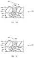
- FIG. 1is a top perspective view of a capture pad structure in accordance with one embodiment of the present invention
- FIG. 2is a cross-sectional view of the capture pad structure along the line II-II of FIG. 1 ;
- FIG. 3is a cross-sectional view of the capture pad structure along the line of FIG. 1 ;
- FIG. 4is a cross-sectional view of the capture pad structure along the line IV-IV of FIG. 1 ;
- FIG. 5is a top perspective view of the capture pad structure of FIG. 1 at a further stage during fabrication in accordance with one embodiment of the present invention
- FIG. 6is a cross-sectional view of the capture pad structure of FIG. 5 along the line VI-VI in accordance with one embodiment
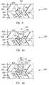
- FIG. 7Ais a cross-sectional view of the capture pad structure of FIG. 6 at a further stage of fabrication in accordance with one embodiment
- FIG. 7Bis a cross-sectional view of a capture pad structure in accordance with another embodiment
- FIG. 7Cis a cross-sectional view of a capture pad structure in accordance with yet another embodiment.
- FIG. 8is a cross-sectional view of a capture pad structure in accordance with another embodiment
- FIG. 9Ais a cross-sectional view of the capture pad structure of FIG. 8 at a further stage of fabrication in accordance with one embodiment
- FIG. 9Bis a cross-sectional view of a capture pad structure in accordance with another embodiment.
- FIG. 9Cis a cross-sectional view of a capture pad structure in accordance with yet another embodiment.
- FIG. 10 ais a cross-sectional view of an electronic component package formed with the capture pad structure of FIG. 9C in accordance with one embodiment
- FIG. 11is a cross-sectional view of an electronic component package formed with the capture pad structure of FIG. 9C in accordance with another embodiment
- FIG. 12is a top perspective view of a capture pad structure in accordance with one embodiment of the present invention.
- FIG. 13is a cross-sectional view of the capture pad structure along the line XIII-XIII of FIG. 12 ;
- FIG. 14is a cross-sectional view of the capture pad structure of FIG. 12 at a further stage of fabrication in accordance with one embodiment.
- FIGS. 15 , 16 , 17 , 18 , 19 , 20are top perspective views of capture pad structures in accordance with various embodiment of the present invention.
- a capture pad structure 100includes a lower dielectric layer 106 , a capture pad 104 embedded within lower dielectric layer 106 , capture pad 104 comprising a plurality of linear segments 108 , 110 .
- capture pad 104is formed using a laser ablation process.
- dielectric layer 106is laser-ablated to form channels therein. More particularly, a focused laser beam is moved linearly, i.e., in straight lines, to form linear channels in dielectric layer 106 . These channels are filled with an electrically conductive material to form capture pad 104 .
- the focused laser beamis moved in a first straight line to form a first channel 122 in dielectric layer 106 in which first linear segment 108 is located and moved in a second straight line to form a second channel 124 in which second linear segment 110 is located.
- the focused laser beamis moved in straight lines rapidly, the laser ablation process used to form capture pad 104 is fast and thus performed at a minimal cost.
- first linear segment 108 and second linear segment 110are less than a circular capture pad having a diameter equal to the length of first linear segment 108 or second linear segment 110 in accordance with this embodiment. Accordingly, the amount of dielectric layer 106 laser-ablated (removed) to form channels 122 , 124 and thus capture pad 104 is minimal. As the amount of dielectric layer 106 removed to form channels 122 , 124 is minimal, the laser ablation process used to form capture pad 104 is fast and thus performed at a minimal cost.
- an upper dielectric layer 602is mounted to lower dielectric layer 106 .
- a blind via aperture 804is formed using a laser ablation over drill process. During this laser ablation over drill process, the energy and ablation time of the focused laser beam is set sufficiently high to laser ablate completely through upper dielectric layer 602 and to partially laser ablate lower dielectric layer 106 around capture pad 104 .
- a blind via 902 with interlocking structure 940is formed within blind via aperture 804 .
- Interlocking structure 940 of blind via 902extends around capture pad 104 . Accordingly, the mechanical strength in the bond between blind via 902 and capture pad 104 is maximized. In this manner, the reliability of the bond between blind via 902 and capture pad 104 is insured.
- FIG. 1is a top perspective view of a capture pad structure 100 in accordance with one embodiment of the present invention.
- FIG. 2is a cross-sectional view of capture pad structure 100 along the line II-II of FIG. 1 .
- FIG. 3is a cross-sectional view of capture pad structure 100 along the line of FIG. 1 .
- FIG. 4is a cross-sectional view of capture pad structure 100 along the line IV-IV of FIG. 1 .
- capture pad structure 100includes a trace 102 , a capture pad 104 , and a lower, e.g., first, dielectric layer 106 .
- Capture pad 104includes a first linear segment 108 and a second linear segment 110 .
- First linear segment 108is linear, i.e., has an absence of curves. More particularly, first linear segment 108 is a straight line extending between a first end 112 and a second end 114 of first linear segment 108 . First linear segment 108 has a uniform width W equal to the width of a focused laser beam used to form the channel in dielectric layer 106 in which first linear segment 108 is formed in one embodiment.
- second linear segment 110is linear, i.e., has an absence of curves. More particularly, second linear segment 110 is a straight line extending between a first end 116 and a second end 118 of second linear segment 110 . Second linear segment 110 also has a uniform width W equal to the width of a focused laser beam used to form the channel in dielectric layer 106 in which second linear segment 110 is formed in one embodiment.
- first linear segment 108has a length, i.e., the distance between first and second ends 112 , 114 , equal to a length of second linear segment 110 , i.e., the distance between first and second ends 116 , 118 .
- first linear segment 108has a length less than or greater than a length of second linear segment 110 .
- First linear segment 108intersects second linear segment 110 at a linear segment intersection 120 .
- first linear segment 108is perpendicular to second linear segment 110 although the angle of intersection of first linear segment 108 to second linear segment 110 is greater or less than 90 degrees in other embodiments.
- perpendicular, parallel, and similar termsare used herein, it is to be understood that the described features may not be exactly perpendicular or parallel, but only substantially perpendicular or parallel to within acceptable manufacturing tolerances.
- First linear segment 108intersects second linear segment 110 in the middle of second linear segment 110 . Accordingly, the distance between first end 116 of second linear segment 110 and intersection 120 equals the distance between second end 118 of second linear segment 110 and intersection 120 .
- second linear segment 110intersects first linear segment 108 in the middle of first linear segment 108 . Accordingly, the distance between first end 112 of first linear segment 108 and intersection 120 equals the distance between second end 114 of first linear segment 108 and intersection 120 .
- first linear segment 108intersects the middle of second linear segment 110 and vice versa
- first linear segment 108intersects second linear segment 110 at a position offset from the middle of second linear segment 110 and/or vice versa.
- Trace 102is electrically connected to intersection 120 and thus to capture pad 104 .
- Trace 102is electrically connected to one or more electrically conductive structures (not shown) of capture pad structure 100 , for example, to lands, solder balls, or other electrically conductive structures on principal surface 106 P and/or lower surface 106 L of dielectric layer 106 .
- Trace 102also has a uniform width W equal to the width of a focused laser beam used to form the channel in dielectric layer 106 in which trace 102 is formed in one embodiment.
- Trace 102is formed of one or more linear segments.
- dielectric layer 106has a principal, e.g., first, surface 106 P and a lower, e.g., second, surface 106 L opposite principal surface 106 P.
- first linear segment 108 , second linear segment 110include exposed upper, e.g., first, surfaces 102 U, 108 U, 110 U, respectively, coplanar, i.e., lying in the same plane, with principal surface 106 P of dielectric layer 106 . Accordingly, upper surfaces 102 U, 108 U, 110 U are exposed from dielectric layer 106 .
- trace 102 , first linear segment 108 , second linear segment 110include coplanar lower, e.g., second, surfaces 102 L, 108 L, 110 L, respectively, below principal surface 106 P of dielectric layer 106 and within dielectric layer 106 . More particularly, lower surfaces 102 L, 108 L, 110 L are located between principal surface 106 P and lower surface 106 L of dielectric layer 106 such that dielectric layer 106 exists between lower surfaces 102 L, 108 L, 110 L and lower surface 106 L.
- trace 102 , first linear segment 108 , second linear segment 110include sidewalls 102 S, 108 S, 110 S extending between upper surfaces 102 U, 108 U, 110 U and lower surfaces 102 L, 108 L, 110 L, respectively.
- trace 102 and capture pad 104are formed using a laser ablation process.
- dielectric layer 106is laser-ablated to form channels therein. More particularly, a focused laser beam is moved linearly, i.e., in straight lines, to form linear channels in dielectric layer 106 having width W equal to the width of the focused laser beam. These channels are filled with an electrically conductive material, e.g., by plating and/or filling with an electrically conductive adhesive, to form trace 102 and capture pad 104 .
- a channelis a trench, opening, or open space in dielectric layer 106 that has a length extending in a horizontal direction parallel to principal surface 106 P of dielectric layer 106 .
- First linear segment 108 , second linear segment 110 , and trace 102are formed of electrically conductive material that fills the channels in dielectric layer 106 .
- the laser ablation process used to form capture pad 104is fast and thus performed at a minimal cost. More particularly, the focused laser beam is moved in a first straight line to form a first channel 122 in dielectric layer 106 in which first linear segment 108 is located and moved in a second straight line to form a second channel 124 in which second linear segment 110 is located. As the focused laser beam is moved in straight lines rapidly, the laser ablation process used to form capture pad 104 is fast and thus performed at a minimal cost.
- first linear segment 108 and second linear segment 110are less than a circular capture pad having a diameter equal to the length of first linear segment 108 or second linear segment 110 in accordance with this embodiment. Accordingly, the amount of dielectric layer 106 laser-ablated (removed) to form channels 122 , 124 and thus capture pad 104 is minimal. As the amount of dielectric layer 106 removed to form channels 122 , 124 is minimal, the laser ablation process used to form capture pad 104 is fast and thus performed at a minimal cost.
- FIG. 5is a top perspective view of capture pad structure 100 of FIG. 1 at a further stage during fabrication in accordance with one embodiment of the present invention.
- FIG. 6is a cross-sectional view of capture pad structure 100 of FIG. 5 along the line VI-VI in accordance with one embodiment.
- an upper, e.g., second, dielectric layer 602is mounted to lower dielectric layer 106 .
- Upper dielectric layer 602is not illustrated in FIG. 5 to allow visualization of capture pad 104 and trace 102 .
- a lower, e.g., first surface 602 L of upper dielectric layer 602is mounted to principal surface 106 P of lower dielectric layer 106 .
- lower surface 602 L of upper dielectric 602 and/or principal surface 106 P of lower dielectric layer 106is adhesive and/or includes an adhesive such that upper dielectric layer 602 is adhesively bonded to lower dielectric layer 106 .
- second dielectric layer 602is applied to lower dielectric layer 106 in a liquid form and then cured, e.g., upper dielectric layer 602 is a cured liquid encapsulant, molding compound, a spin on coating, or other cured material.
- a blind via aperture 604is formed through upper dielectric layer 602 , e.g., using laser ablation.
- Blind via aperture 604extends through upper dielectric layer 602 from an upper, e.g., second, surface 602 U to lower surface 602 L and to capture pad 104 .
- Blind via aperture 604is defined by a blind via aperture sidewall 604 S that extends from upper surface 602 U to lower surface 602 L.
- blind via aperture 604is aligned with capture pad 104 . More particularly, a portion of capture pad 104 is exposed through blind via aperture 604 .
- the length of first linear segment 108 and second linear segment 110is greater than a diameter D of blind via aperture 604 at lower surface 602 L of upper dielectric layer 602 . Accordingly, tolerance in the registration (positioning) of blind via aperture 604 relative to capture pad 104 is accommodated.
- FIG. 7Ais a cross-sectional view of capture pad structure 100 of FIG. 6 at a further stage of fabrication in accordance with one embodiment.
- an electrically conductive blind via 702is formed within blind via aperture 604 .
- Blind via 702e.g., an electrically conductive plated copper seed layer, is formed on blind via aperture sidewall 604 S and extends from upper surface 602 U to lower surface 602 L of upper dielectric layer 602 .
- Blind via 702i.e., a hollow via, does not completely fill blind via aperture 604 such that a space 704 exists within blind via 702 .
- Blind via 702is electrically connected to (e.g., plated on) capture pad 104 . Accordingly, blind via 702 forms the electrical connection to capture pad 104 through upper dielectric layer 602 .
- FIG. 7Bis a cross-sectional view of a capture pad structure 100 B in accordance with another embodiment.
- Capture pad structure 100 B of FIG. 7Bis similar to capture pad structure 100 of FIG. 7A and only the significant differences are discussed below.
- a blind via 712is a multilayer blind via including a hollow blind via 702 and a hollow via filling 706 .
- Hollow blind via 702is substantially similar to blind via 702 of capture pad structure 100 of FIG. 7A .
- Hollow via filling 706is electrically conductive material, e.g., plated metal, solder or electrically conductive adhesive, which fills the space within hollow blind via 702 .
- blind via 712has a planar upper surface 712 U, e.g., a contact or land, coplanar with upper surface 602 U of upper dielectric layer 602 .
- FIG. 7Cis a cross-sectional view of a capture pad structure 100 C in accordance with yet another embodiment.
- Capture pad structure 100 C of FIG. 7Cis similar to capture pad structure 100 of FIG. 7A and only the significant differences are discussed below.
- a blind via 722is electrically conductive material, e.g., plated metal, solder or electrically conductive adhesive, which fills blind via aperture 604 .
- Blind via 722extends from upper surface 602 U to lower surface 602 L of upper dielectric layer 602 .
- Blind via 722completely fills blind via aperture 604 .
- blind via 722has a planar upper surface 722 U, e.g., a contact or land, coplanar with upper surface 602 U of upper dielectric layer 602 .
- Blind via 722is electrically connected to capture pad 104 . Accordingly, blind via 722 forms the electrical connection to capture pad 104 through upper dielectric layer 602 .
- FIG. 8is a cross-sectional view of a capture pad structure 100 D in accordance with another embodiment.
- Capture pad structure 100 D of FIG. 8is similar to capture pad structure 100 of FIG. 6 and only the significant differences are discussed below.
- a blind via aperture 804is formed through upper dielectric layer 602 , e.g., using laser ablation.
- Blind via aperture 804extends through upper dielectric layer 602 from upper surface 602 U to lower surface 602 L and to capture pad 104 .
- Blind via aperture 804is defined by a blind via aperture sidewall 804 S that extends from upper surface 602 U to lower surface 602 L and partially into lower dielectric layer 106 .
- Blind via aperture 804extends into lower dielectric layer 106 around capture pad 104 .
- Blind via aperture 804is formed using a laser ablation over drill process. During this laser ablation over drill process, the energy and ablation time of the focused laser beam, e.g., a low fluence laser beam, is set sufficiently high to laser ablate completely through upper dielectric layer 602 and to partially laser ablate lower dielectric layer 106 around capture pad 104 .
- the focused laser beame.g., a low fluence laser beam
- Dielectric layer 106e.g., molding compound, laminate material, flexible tape, or other dielectric material, is selectively laser ablated relative to capture pad 104 , e.g., an electrically conductive material such as copper. Stated another way, dielectric layer 106 is laser ablated (removed) by the focused laser beam whereas capture pad 104 is substantially unaffected by the focused laser beam. Accordingly, during the laser ablation over drill process, dielectric layer 106 is removed around capture pad 104 .
- dielectric layer 106is over drilled such that a portion of the sidewalls of capture pad 104 is exposed by blind via aperture 804 .
- the lower surface of capture pad 104remains embedded and in contact with lower dielectric layer 106 .
- lower dielectric layer 106is removed around an upper, e.g., first, portion 830 of sidewalls 108 S of first linear segment 108 as illustrated in FIG. 8 .
- a lower, e.g., second, portion 832 of sidewalls 108 S of first linear segment 108remains embedded and in contact with lower dielectric layer 106 .
- blind via aperture 804is aligned with capture pad 104 . More particularly, a portion of capture pad 104 is exposed through blind via aperture 804 .
- the length of first linear segment 108 and second linear segment 110is greater than a diameter D of blind via aperture 804 at lower surface 602 L of upper dielectric layer 602 . Accordingly, tolerance in the registration (positioning) of blind via aperture 804 relative to capture pad 104 is accommodated.
- FIG. 9Ais a cross-sectional view of capture pad structure 100 D of FIG. 8 at a further stage of fabrication in accordance with one embodiment.
- an electrically conductive blind via 902is formed within blind via aperture 804 .
- Blind via 902e.g., an electrically conductive plated copper seed layer, is formed on blind via aperture sidewall 804 S and extends from upper surface 602 U to lower surface 602 L of upper dielectric layer 602 .
- Blind via 902i.e., a hollow via, does not completely fill blind via aperture 804 such that a space 904 exists within blind via 902 .
- Blind via 902is electrically connected to (e.g., plated on) capture pad 104 .
- Blind via 902extends around capture pad 104 . More particularly, blind via 902 directly contacts the upper surface of capture pad 104 and a portion of the sidewalls of capture pad 104 .
- blind via 902contacts upper surface 108 U and upper portion 830 of sidewalls 108 S of first linear segment 108 as illustrated in FIG. 9A . Accordingly, blind via 902 forms the electrical connection to capture pad 104 through upper dielectric layer 602 .
- interlocking structure 940 of blind via 902extends around capture pad 104 .
- the mechanical strength in the bond between blind via 902 and capture pad 104is maximized. In this manner, the reliability of the bond between blind via 902 and capture pad 104 is insured.
- FIG. 9Bis a cross-sectional view of a capture pad structure 100 E in accordance with another embodiment.
- Capture pad structure 100 E of FIG. 9Bis similar to capture pad structure 100 D of FIG. 9A and only the significant differences are discussed below.
- a blind via 912is a multilayer blind via including a hollow blind via 902 and a hollow via filling 906 .
- Hollow blind via 902is substantially similar to blind via 902 of capture pad structure 100 D of FIG. 9A .
- Hollow via filling 906is electrically conductive material, e.g., plated metal, solder or electrically conductive adhesive, which fills the space within hollow blind via 902 .
- blind via 912has a planar upper surface 912 U, e.g., a contact or land, coplanar with upper surface 602 U of upper dielectric layer 602 .
- FIG. 9Cis a cross-sectional view of a capture pad structure 100 F in accordance with yet another embodiment.
- Capture pad structure 100 F of FIG. 9Cis similar to capture pad structure 100 D of FIG. 9A and only the significant differences are discussed below.
- a blind via 922is electrically conductive material, e.g., plated metal, solder or electrically conductive adhesive, which fills blind via aperture 804 .
- Blind via 922extends from upper surface 602 U to lower surface 602 L of upper dielectric layer 602 .
- Blind via 922completely fills blind via aperture 804 .
- blind via 922has a planar upper surface 922 U, e.g., a contact or land, coplanar with upper surface 602 U of upper dielectric layer 602 .
- Blind via 922is electrically connected to capture pad 104 .
- Blind via 922extends around capture pad 104 . More particularly, blind via 922 directly contacts the upper surface of capture pad 104 and a portion of the sidewalls of capture pad 104 .
- blind via 922contacts upper surface 108 U and upper portion 830 of sidewalls 108 S of first linear segment 108 as illustrated in FIG. 9C . Accordingly, blind via 922 forms the electrical connection to capture pad 104 through upper dielectric layer 602 .
- interlocking structure 940 of blind via 922extends around capture pad 104 .
- the mechanical strength in the bond between blind via 922 and capture pad 104is maximized. In this manner, the reliability of the bond between blind via 922 and capture pad 104 is insured.
- dielectric layers 106 , 602are illustrated, in light of this disclosure, those of skill in the art will understand that embodiments of the present invention are applicable to any multi-layer substrates needing inter-layer connections, e.g., having two or more dielectric layers.
- FIG. 10is a cross-sectional view of an electronic component package 1000 formed with capture pad structure 100 F of FIG. 9C in accordance with one embodiment.
- capture pad structure 100 Fforms the substrate for package 1000 .
- Package 1000includes an electronic component 1002 , e.g., an active component such as an integrated circuit die, or a passive component such as a resistor, capacitor, or inductor.
- electronic component 1002is herein referred to as integrated circuit die 1002 .
- An inactive, e.g., first, surface 1002 I of integrated circuit die 1002is mounted to upper surface 602 U of upper dielectric layer 602 by an adhesive 1004 , sometimes called a die attach adhesive.
- An active, e.g., second, surface 1002 A of integrated circuit die 1002includes a bond pad 1008 formed thereon.
- Bond pad 1008is electrically connected to upper surface 922 U of blind via 922 by a bond wire 1010 .
- Integrated circuit die 1002 , bond wire 1010 , and at least a portion of upper surface 602 U of upper dielectric layer 602are enclosed within, sometimes called encapsulated, within an encapsulant 1012 .
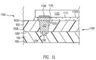
- FIG. 11is a cross-sectional view of an electronic component package 1100 formed with capture pad structure 100 F of FIG. 9C in accordance with another embodiment.
- capture pad structure 100 Fforms the substrate for package 1100 .
- Package 1100includes an electronic component 1102 mounted in a flip chip configuration.
- Electronic component 1102is an active component such as an integrated circuit die, or a passive component such as a resistor, capacitor, or inductor.
- electronic component 1102is herein referred to as integrated circuit die 1102 .
- An active, e.g., first, surface 1102 A of integrated circuit die 1102includes a bond pad 1108 formed thereon.
- Bond pad 1108is electrically connected to upper surface 922 U of blind via 922 by a flip chip bump 1110 , e.g., solder.
- an underfill 1112is applied between active surface 1102 A and upper surface 602 U of upper dielectric layer 602 and around flip chip bump 1110 .
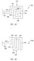
- FIG. 12is a top perspective view of a capture pad structure 1200 in accordance with one embodiment of the present invention.
- FIG. 13is a cross-sectional view of capture pad structure 1200 along the line XIII-XIII of FIG. 12 .
- Capture pad structure 1200 of FIGS. 12 , 13is similar to capture pad structure 100 of FIGS. 5 , 6 and only the significant differences are discussed below.
- capture pad structure 1200includes trace 102 , capture pad 104 , lower dielectric layer 106 , and upper dielectric layer 602 .
- a via aperture 1304is formed through upper dielectric layer 602 and lower dielectric layer 106 .
- Via aperture 1304extends through upper dielectric layer 602 and lower dielectric layer 106 from upper surface 602 U of upper dielectric layer 602 to lower surface 106 L of lower dielectric layer 106 .
- Via aperture 1304extends through capture pad 104 .
- Via aperture 1304is defined by a via aperture sidewall 1304 S that extends from upper surface 602 U to lower surface 106 L.
- via aperture 1304is aligned with capture pad 104 . More particularly, via aperture 1304 passes through a portion of capture pad 104 . The length of first linear segment 108 and second linear segment 110 is greater than a diameter D of via aperture 1304 . Accordingly, tolerance in the registration (positioning) of via aperture 1304 relative to capture pad 104 is accommodated.
- Via aperture 1304is formed by mechanical drilling, laser ablation, chemical etching, or other via aperture fabrication process.
- FIG. 14is a cross-sectional view of capture pad structure 1200 of FIG. 12 at a further stage of fabrication in accordance with one embodiment.
- an electrically conductive via 1402is formed within via aperture 1304 .
- Via 1402e.g., an electrically conductive plated copper layer, is formed on via aperture sidewall 1304 S and extends from upper surface 602 U to lower surface 106 L.
- Via 1402i.e., a hollow via, does not completely fill via aperture 1304 such that a space 1404 exists within via 1402 .
- via 1402entirely fills via aperture 1304 .
- Via 1402is electrically connected to capture pad 104 . Accordingly, via 1402 forms the electrical connection to capture pad 104 through upper dielectric layer 602 and also through lower dielectric layer 106 .
- capture pad 104is a plurality of linear segments arranged into a star configuration
- a capture pad in accordance with other embodiments of the present inventionis formed of a plurality of linear segment arranged in other configurations such as those illustrated in FIGS. 15 , 16 , 17 , 18 , 19 , and 20 .
- FIG. 15is a top perspective view of a capture pad structure 1500 in accordance with another embodiment of the present invention.
- Capture pad structure 1500 of FIG. 15is similar to capture pad structure 100 of FIG. 1 and only the significant differences are discussed below.
- capture pad structure 1500includes a trace 102 A, a capture pad 104 A, and a dielectric layer 106 A.
- Capture pad 104 Asometimes called a cross configuration capture pad, includes a plurality of interconnected linear segments, i.e., three linear segments 1550 , 1552 , and 1554 . Linear segments 1550 , 1552 , 1554 are joined together at a linear segment intersection 1520 .
- Trace 102 Aextends from and is coupled to linear segment intersection 1520 .
- Linear segment 1550extends from linear segment intersection 1520 in a direction perpendicular to trace 102 A.
- Linear segment 1552extends from linear segment intersection 1520 in a direction parallel to but opposite from trace 102 A, and perpendicular to linear segments 1550 , 1554 .
- Linear segment 1554extends from linear segment intersection 1520 in a direction perpendicular to trace 102 A and opposite linear segment 1550 .
- FIG. 16is a top perspective view of a capture pad structure 1600 in accordance with another embodiment of the present invention.
- Capture pad structure 1600 of FIG. 16is similar to capture pad structure 1500 of FIG. 15 and only the significant differences are discussed below.
- capture pad structure 1600includes a trace 102 B, a capture pad 104 B, and a dielectric layer 106 B.
- Capture pad 104 Bsometimes called a horizontal bars configuration capture pad, includes a plurality of interconnected linear segments, i.e., linear segments 1550 , 1552 , 1554 , 1650 , 1652 .
- linear segment 1550extends from linear segment intersection 1520 to linear segment 1650 and in a direction perpendicular to trace 102 B.
- Linear segment 1650is parallel to trace 102 B and perpendicular to linear segment 1550 . Further, linear segment 1550 is coupled to the middle of linear segment 1650 .
- linear segment 1554extends from linear segment intersection 1520 to linear segment 1652 and in a direction perpendicular to trace 102 B.
- Linear segment 1652is parallel to trace 102 B and perpendicular to linear segment 1554 . Further, linear segment 1554 is coupled the middle of linear segment 1652 .
- FIG. 17is a top perspective view of a capture pad structure 1700 in accordance with another embodiment of the present invention. Capture pad structure 1700 of FIG. 17 is similar to capture pad structure 100 of FIG. 1 and only the significant differences are discussed below.
- capture pad structure 1700includes a trace 102 C, a capture pad 104 C, and a dielectric layer 106 C.
- Capture pad 104 Csometimes called a spokes configuration capture pad, includes a plurality of interconnected linear segments, i.e., linear segments 1750 , 1752 , 1754 , 1756 , 1758 interconnected at a linear segment intersection 1720 , sometimes called hub.
- linear segments 1750 , 1752 , 1754 , 1756 , 1758 and trace 102 Cextend radially outwards from linear segment intersection 1720 .
- FIG. 18is a top perspective view of a capture pad structure 1800 in accordance with another embodiment of the present invention. Capture pad structure 1800 of FIG. 18 is similar to capture pad structure 1500 of FIG. 15 and only the significant differences are discussed below.
- capture pad structure 1800includes a trace 102 D, a capture pad 104 D, and a dielectric layer 106 D.
- Capture pad 104 Dsometimes called a vertical bars configuration capture pad, includes a plurality of interconnected linear segments, i.e., linear segments 1550 , 1552 , 1554 , 1850 , 1852 , 1854 , 1856 .
- linear segment 1552extends from linear segment intersection 1520 to a second linear segment intersection 1820 and in a direction parallel to but opposite trace 102 D.
- Linear segment 1850extends from linear segment intersection 1820 in a direction perpendicular to linear segment 1552 .
- Linear segment 1854extends from linear segment intersection 1820 in a direction parallel to but opposite from linear segment 1552 , and perpendicular to linear segments 1850 , 1852 .
- Linear segment 1852extends from linear segment intersection 1820 in a direction perpendicular to linear segment 1552 and opposite linear segment 1850 .
- Linear segment 1854extends from linear segment intersection 1820 to linear segment 1856 .
- Linear segment 1854is perpendicular to linear segment 1856 . Further, linear segment 1854 is coupled to the middle of linear segment 1856 .
- FIG. 19is a top perspective view of a capture pad structure 1900 in accordance with another embodiment of the present invention.
- Capture pad structure 1900 of FIG. 19is similar to capture pad structure 100 of FIG. 1 and only the significant differences are discussed below.
- capture pad structure 1900includes a trace 102 E, a capture pad 104 E, and a dielectric layer 106 E.
- Capture pad 104 Esometimes called a maze configuration capture pad, includes a plurality of interconnected linear segments, i.e., linear segments 1950 , 1952 , 1954 , 1956 , 1958 , 1960 , 1962 .
- Linear segment 1950extends perpendicularly from trace 102 E to linear segment 1952 .
- Linear segment 1952extends perpendicularly from linear segment 1950 in a direction opposite but parallel to trace 102 E to linear segment 1954 .
- Linear segment 1954extends perpendicularly from linear segment 1952 in a same direction and parallel to linear segment 1950 to linear segment 1956 .
- Linear segment 1956extends perpendicularly from linear segment 1954 in a same direction and parallel to linear segment 1952 to linear segment 1958 .
- Linear segment 1958extends perpendicularly from linear segment 1956 in a same direction and parallel to linear segment 1954 to linear segment 1960 .
- Linear segment 1960extends perpendicularly from linear segment 1958 in a same direction and parallel to linear segment 1956 to linear segment 1962 .
- Linear segment 1962extends perpendicularly from linear segment 1960 in a same direction and parallel to linear segment 1958 .
- FIG. 20is a top perspective view of a capture pad structure 2000 in accordance with another embodiment of the present invention.
- Capture pad structure 2000 of FIG. 20is similar to capture pad structure 100 of FIG. 1 and only the significant differences are discussed below.
- capture pad structure 2000includes a trace 102 F, a capture pad 104 F, and a dielectric layer 106 F.
- Capture pad 104 Fsometimes called a serpentine configuration capture pad, includes a plurality of interconnected linear segments, i.e., linear segments 2050 , 2052 , 2054 , 2056 , 2058 , 2060 , 2062 .
- Linear segment 2050extends perpendicularly from trace 102 F to linear segment 2052 .
- Linear segment 2052extends perpendicularly from linear segment 2050 in a direction opposite but parallel to trace 102 F to linear segment 2054 .
- Linear segment 2054extends perpendicularly from linear segment 2052 in a same direction and parallel to linear segment 2050 to linear segment 2056 .
- Linear segment 2056extends perpendicularly from linear segment 2054 in an opposite direction and parallel to linear segment 2052 to linear segment 2058 .
- Linear segment 2058extends perpendicularly from linear segment 2056 in a same direction and parallel to linear segment 2054 to linear segment 2060 .
- Linear segment 2060extends perpendicularly from linear segment 2058 in an opposite direction and parallel to linear segment 2056 to linear segment 2062 .
- Linear segment 2062extends perpendicularly from linear segment 2060 in a same direction and parallel to linear segment 2058 .
Landscapes
- Engineering & Computer Science (AREA)
- Physics & Mathematics (AREA)
- Microelectronics & Electronic Packaging (AREA)
- Condensed Matter Physics & Semiconductors (AREA)
- General Physics & Mathematics (AREA)
- Computer Hardware Design (AREA)
- Power Engineering (AREA)
- Geometry (AREA)
- Ceramic Engineering (AREA)
- Manufacturing & Machinery (AREA)
- Production Of Multi-Layered Print Wiring Board (AREA)
Abstract
Description
Claims (19)
Priority Applications (1)
| Application Number | Priority Date | Filing Date | Title |
|---|---|---|---|
| US12/800,757US8671565B1 (en) | 2006-12-22 | 2010-05-21 | Blind via capture pad structure fabrication method |
Applications Claiming Priority (2)
| Application Number | Priority Date | Filing Date | Title |
|---|---|---|---|
| US11/615,467US7750250B1 (en) | 2006-12-22 | 2006-12-22 | Blind via capture pad structure |
| US12/800,757US8671565B1 (en) | 2006-12-22 | 2010-05-21 | Blind via capture pad structure fabrication method |
Related Parent Applications (1)
| Application Number | Title | Priority Date | Filing Date |
|---|---|---|---|
| US11/615,467DivisionUS7750250B1 (en) | 2006-12-22 | 2006-12-22 | Blind via capture pad structure |
Publications (1)
| Publication Number | Publication Date |
|---|---|
| US8671565B1true US8671565B1 (en) | 2014-03-18 |
Family
ID=42307013
Family Applications (2)
| Application Number | Title | Priority Date | Filing Date |
|---|---|---|---|
| US11/615,467Active2028-03-05US7750250B1 (en) | 2006-12-22 | 2006-12-22 | Blind via capture pad structure |
| US12/800,757Active2029-08-01US8671565B1 (en) | 2006-12-22 | 2010-05-21 | Blind via capture pad structure fabrication method |
Family Applications Before (1)
| Application Number | Title | Priority Date | Filing Date |
|---|---|---|---|
| US11/615,467Active2028-03-05US7750250B1 (en) | 2006-12-22 | 2006-12-22 | Blind via capture pad structure |
Country Status (1)
| Country | Link |
|---|---|
| US (2) | US7750250B1 (en) |
Cited By (2)
| Publication number | Priority date | Publication date | Assignee | Title |
|---|---|---|---|---|
| CN109548271A (en)* | 2018-11-14 | 2019-03-29 | 江门崇达电路技术有限公司 | A kind of production method of the printed circuit board for signal generator |
| US10334728B2 (en)* | 2016-02-09 | 2019-06-25 | Advanced Semiconductor Engineering, Inc. | Reduced-dimension via-land structure and method of making the same |
Families Citing this family (6)
| Publication number | Priority date | Publication date | Assignee | Title |
|---|---|---|---|---|
| KR100771862B1 (en)* | 2005-08-12 | 2007-11-01 | 삼성전자주식회사 | Printed circuit board, manufacturing method and memory module-socket assembly for memory module |
| KR100771467B1 (en)* | 2006-10-30 | 2007-10-30 | 삼성전기주식회사 | Circuit board and manufacturing method |
| US7932170B1 (en) | 2008-06-23 | 2011-04-26 | Amkor Technology, Inc. | Flip chip bump structure and fabrication method |
| US9935038B2 (en)* | 2012-04-11 | 2018-04-03 | Taiwan Semiconductor Manufacturing Company | Semiconductor device packages and methods |
| US9536850B2 (en)* | 2013-03-08 | 2017-01-03 | Taiwan Semiconductor Manufacturing Company, Ltd. | Package having substrate with embedded metal trace overlapped by landing pad |
| US9129843B1 (en)* | 2014-06-12 | 2015-09-08 | Globalfoundries Inc. | Integrated inductor |
Citations (138)
| Publication number | Priority date | Publication date | Assignee | Title |
|---|---|---|---|---|
| US3833838A (en) | 1972-11-13 | 1974-09-03 | A Christiansen | Electronic component mounting wafers for repeated connection in a variety of circuit designs |
| US3868724A (en) | 1973-11-21 | 1975-02-25 | Fairchild Camera Instr Co | Multi-layer connecting structures for packaging semiconductor devices mounted on a flexible carrier |
| US3916434A (en) | 1972-11-30 | 1975-10-28 | Power Hybrids Inc | Hermetically sealed encapsulation of semiconductor devices |
| US4322778A (en) | 1980-01-25 | 1982-03-30 | International Business Machines Corp. | High performance semiconductor package assembly |
| US4532419A (en) | 1982-09-09 | 1985-07-30 | Sony Corporation | Memory card having static electricity protection |
| US4642160A (en) | 1985-08-12 | 1987-02-10 | Interconnect Technology Inc. | Multilayer circuit board manufacturing |
| US4685033A (en) | 1984-08-28 | 1987-08-04 | Nec Corporation | Multilayer wiring substrate |
| US4706167A (en) | 1983-11-10 | 1987-11-10 | Telemark Co., Inc. | Circuit wiring disposed on solder mask coating |
| US4716049A (en) | 1985-12-20 | 1987-12-29 | Hughes Aircraft Company | Compressive pedestal for microminiature connections |
| US4786952A (en) | 1986-07-24 | 1988-11-22 | General Motors Corporation | High voltage depletion mode MOS power field effect transistor |
| US4811082A (en) | 1986-11-12 | 1989-03-07 | International Business Machines Corporation | High performance integrated circuit packaging structure |
| US4897338A (en) | 1987-08-03 | 1990-01-30 | Allied-Signal Inc. | Method for the manufacture of multilayer printed circuit boards |
| US4905124A (en) | 1987-03-31 | 1990-02-27 | Mitsubishi Denki Kabushiki Kaisha | IC card |
| US4964212A (en) | 1988-09-29 | 1990-10-23 | Commissariat A L'energie Atomique | Process for producing electrical connections through a substrate |
| US4974120A (en) | 1989-01-12 | 1990-11-27 | Mitsubishi Denki Kabushiki Kaisha | IC card |
| US4996391A (en) | 1988-09-30 | 1991-02-26 | Siemens Aktiengesellschaft | Printed circuit board having an injection molded substrate |
| US5021047A (en) | 1989-08-29 | 1991-06-04 | Movern John B | Restricted use hypodermic syringe |
| US5072075A (en) | 1989-06-28 | 1991-12-10 | Digital Equipment Corporation | Double-sided hybrid high density circuit board and method of making same |
| US5081520A (en) | 1989-05-16 | 1992-01-14 | Minolta Camera Kabushiki Kaisha | Chip mounting substrate having an integral molded projection and conductive pattern |
| US5108553A (en) | 1989-04-04 | 1992-04-28 | Olin Corporation | G-tab manufacturing process and the product produced thereby |
| US5110664A (en) | 1989-07-10 | 1992-05-05 | Hitachi, Ltd. | Thick film and thin film composite substrate and electronic circuit apparatus using it |
| US5191174A (en) | 1990-08-01 | 1993-03-02 | International Business Machines Corporation | High density circuit board and method of making same |
| US5209817A (en)* | 1991-08-22 | 1993-05-11 | International Business Machines Corporation | Selective plating method for forming integral via and wiring layers |
| US5229550A (en) | 1990-10-30 | 1993-07-20 | International Business Machines Corporation | Encapsulated circuitized power core alignment and lamination |
| US5239448A (en) | 1991-10-28 | 1993-08-24 | International Business Machines Corporation | Formulation of multichip modules |
| US5247429A (en) | 1990-11-21 | 1993-09-21 | Nippondenso Co., Ltd. | Display board |
| US5283459A (en) | 1989-11-15 | 1994-02-01 | Kabushiki Kaisha Toshiba | Semiconductor sensor including an aperture having a funnel shaped section intersecting a second section |
| US5371654A (en) | 1992-10-19 | 1994-12-06 | International Business Machines Corporation | Three dimensional high performance interconnection package |
| US5379191A (en) | 1991-02-26 | 1995-01-03 | Microelectronics And Computer Technology Corporation | Compact adapter package providing peripheral to area translation for an integrated circuit chip |
| US5404044A (en) | 1992-09-29 | 1995-04-04 | International Business Machines Corporation | Parallel process interposer (PPI) |
| US5463253A (en) | 1990-03-15 | 1995-10-31 | Fujitsu Limited | Semiconductor device having a plurality of chips |
| US5474957A (en) | 1994-05-09 | 1995-12-12 | Nec Corporation | Process of mounting tape automated bonded semiconductor chip on printed circuit board through bumps |
| US5474958A (en) | 1993-05-04 | 1995-12-12 | Motorola, Inc. | Method for making semiconductor device having no die supporting surface |
| US5508938A (en) | 1992-08-13 | 1996-04-16 | Fujitsu Limited | Special interconnect layer employing offset trace layout for advanced multi-chip module packages |
| US5530288A (en) | 1994-10-12 | 1996-06-25 | International Business Machines Corporation | Passive interposer including at least one passive electronic component |
| US5531020A (en) | 1989-11-14 | 1996-07-02 | Poly Flex Circuits, Inc. | Method of making subsurface electronic circuits |
| US5574309A (en) | 1991-11-25 | 1996-11-12 | Gemplus Card International | Integrated circuit card comprising means for the protection of the integrated circuit |
| US5581498A (en) | 1993-08-13 | 1996-12-03 | Irvine Sensors Corporation | Stack of IC chips in lieu of single IC chip |
| US5582858A (en) | 1991-10-07 | 1996-12-10 | International Business Machines Corporation | Adhesive layer in multi-level packaging and organic material as a metal diffusion barrier |
| US5616422A (en) | 1994-02-28 | 1997-04-01 | International Business Machines Corporation | Metallized substrate |
| US5637832A (en) | 1993-10-26 | 1997-06-10 | Pacific Microelectronics Corporation | Solder ball array and method of preparation |
| US5674785A (en) | 1995-11-27 | 1997-10-07 | Micron Technology, Inc. | Method of producing a single piece package for semiconductor die |
| US5719749A (en) | 1994-09-26 | 1998-02-17 | Sheldahl, Inc. | Printed circuit assembly with fine pitch flexible printed circuit overlay mounted to printed circuit board |
| US5739588A (en) | 1994-08-15 | 1998-04-14 | Citizen Watch Co., Ltd. | Semiconductor device |
| US5739581A (en) | 1995-11-17 | 1998-04-14 | National Semiconductor Corporation | High density integrated circuit package assembly with a heatsink between stacked dies |
| US5742479A (en) | 1994-03-09 | 1998-04-21 | Seiko Epson Corporation | Card-type electronic device with plastic frame sandwiched between printed circuit board and metal panel |
| US5744224A (en) | 1994-11-29 | 1998-04-28 | Shinko Electric Industries Co., Ltd. | Board for mounting semiconductor chip |
| US5774340A (en) | 1996-08-28 | 1998-06-30 | International Business Machines Corporation | Planar redistribution structure and printed wiring device |
| US5796590A (en) | 1996-11-05 | 1998-08-18 | Micron Electronics, Inc. | Assembly aid for mounting packaged integrated circuit devices to printed circuit boards |
| US5798014A (en) | 1995-02-02 | 1998-08-25 | Hestia Technologies, Inc. | Methods of making multi-tier laminate substrates for electronic device packaging |
| US5822190A (en) | 1996-06-11 | 1998-10-13 | Kabushiki Kaisha Toshiba | Card type memory device and a method for manufacturing the same |
| US5826330A (en) | 1995-12-28 | 1998-10-27 | Hitachi Aic Inc. | Method of manufacturing multilayer printed wiring board |
| US5835355A (en) | 1997-09-22 | 1998-11-10 | Lsi Logic Corporation | Tape ball grid array package with perforated metal stiffener |
| US5847453A (en) | 1996-03-27 | 1998-12-08 | Honda Giken Kogyo Kabushiki Kaisha | Microwave circuit package |
| US5872399A (en) | 1996-04-01 | 1999-02-16 | Anam Semiconductor, Inc. | Solder ball land metal structure of ball grid semiconductor package |
| US5894108A (en) | 1997-02-11 | 1999-04-13 | National Semiconductor Corporation | Plastic package with exposed die |
| US5903052A (en) | 1998-05-12 | 1999-05-11 | Industrial Technology Research Institute | Structure for semiconductor package for improving the efficiency of spreading heat |
| US5928767A (en) | 1995-06-07 | 1999-07-27 | Dexter Corporation | Conductive film composite |
| US5936843A (en) | 1997-10-14 | 1999-08-10 | Fujitsu Limited | Printed wiring board with mounted circuit element using a terminal density conversion board |
| US5952611A (en) | 1997-12-19 | 1999-09-14 | Texas Instruments Incorporated | Flexible pin location integrated circuit package |
| US6004619A (en) | 1996-11-07 | 1999-12-21 | Hewlett-Packard Company | Process for manufacturing printed circuit boards |
| US6013948A (en) | 1995-11-27 | 2000-01-11 | Micron Technology, Inc. | Stackable chip scale semiconductor package with mating contacts on opposed surfaces |
| US6021564A (en) | 1996-11-08 | 2000-02-08 | W. L. Gore & Associates, Inc. | Method for reducing via inductance in an electronic assembly and article |
| US6028364A (en) | 1994-09-20 | 2000-02-22 | Hitachi, Ltd. | Semiconductor device having a stress relieving mechanism |
| US6034427A (en) | 1998-01-28 | 2000-03-07 | Prolinx Labs Corporation | Ball grid array structure and method for packaging an integrated circuit chip |
| US6035527A (en) | 1996-05-18 | 2000-03-14 | Ingenieurbuero Tamm Factory Innovations | Method for the production of printed circuit boards |
| US6040622A (en) | 1998-06-11 | 2000-03-21 | Sandisk Corporation | Semiconductor package using terminals formed on a conductive layer of a circuit board |
| US6060778A (en) | 1997-05-17 | 2000-05-09 | Hyundai Electronics Industries Co. Ltd. | Ball grid array package |
| US6064576A (en) | 1997-01-02 | 2000-05-16 | Texas Instruments Incorporated | Interposer having a cantilevered ball connection and being electrically connected to a printed circuit board |
| US6069407A (en) | 1998-11-18 | 2000-05-30 | Vlsi Technology, Inc. | BGA package using PCB and tape in a die-up configuration |
| US6072243A (en) | 1996-11-26 | 2000-06-06 | Sharp Kabushiki Kaisha | Semiconductor integrated circuit device capable of surely electrically insulating two semiconductor chips from each other and fabricating method thereof |
| US6081036A (en) | 1996-04-19 | 2000-06-27 | Matsushita Electronics Corp. | Semiconductor device |
| US6119338A (en) | 1998-03-19 | 2000-09-19 | Industrial Technology Research Institute | Method for manufacturing high-density multilayer printed circuit boards |
| US6122171A (en) | 1999-07-30 | 2000-09-19 | Micron Technology, Inc. | Heat sink chip package and method of making |
| US6127833A (en) | 1999-01-04 | 2000-10-03 | Taiwan Semiconductor Manufacturing Co. | Test carrier for attaching a semiconductor device |
| US6160705A (en) | 1997-05-09 | 2000-12-12 | Texas Instruments Incorporated | Ball grid array package and method using enhanced power and ground distribution circuitry |
| US6172419B1 (en) | 1998-02-24 | 2001-01-09 | Micron Technology, Inc. | Low profile ball grid array package |
| US6175087B1 (en) | 1998-12-02 | 2001-01-16 | International Business Machines Corporation | Composite laminate circuit structure and method of forming the same |
| US6184463B1 (en) | 1998-04-13 | 2001-02-06 | Harris Corporation | Integrated circuit package for flip chip |
| US6194250B1 (en) | 1998-09-14 | 2001-02-27 | Motorola, Inc. | Low-profile microelectronic package |
| US6204453B1 (en) | 1998-12-02 | 2001-03-20 | International Business Machines Corporation | Two signal one power plane circuit board |
| US6214641B1 (en) | 1996-06-25 | 2001-04-10 | Micron Technology, Inc. | Method of fabricating a multi-chip module |
| US6228466B1 (en) | 1997-04-11 | 2001-05-08 | Ibiden Co. Ltd. | Printed wiring board and method for manufacturing the same |
| US6239485B1 (en) | 1998-11-13 | 2001-05-29 | Fujitsu Limited | Reduced cross-talk noise high density signal interposer with power and ground wrap |
| USD445096S1 (en) | 1998-04-01 | 2001-07-17 | Sandisk Corporation | Removable memory card for use with portable electronic devices |
| USD446525S1 (en) | 1999-08-24 | 2001-08-14 | Kabushiki Kaisha Toshiba | IC memory card |
| US6274821B1 (en) | 1998-09-16 | 2001-08-14 | Denso Corporation | Shock-resistive printed circuit board and electronic device including the same |
| US6280641B1 (en) | 1998-06-02 | 2001-08-28 | Mitsubishi Gas Chemical Company, Inc. | Printed wiring board having highly reliably via hole and process for forming via hole |
| US6316285B1 (en) | 1998-09-02 | 2001-11-13 | Micron Technology, Inc. | Passivation layer for packaged integrated circuits |
| US20020017712A1 (en) | 1998-06-04 | 2002-02-14 | Yoshihiro Bessho | Method for fabricating a semiconductor package with a semiconductor device attached to a multilayered substrate |
| US6351031B1 (en) | 1999-10-12 | 2002-02-26 | Fujitsu Limited | Semiconductor device and method for manufacturing substrate of the same |
| US6353999B1 (en) | 1999-03-09 | 2002-03-12 | Unimicron Taiwan Corp. | Method of making mechanical-laser structure |
| US6365975B1 (en) | 1997-04-02 | 2002-04-02 | Tessera, Inc. | Chip with internal signal routing in external element |
| US6376906B1 (en) | 1997-02-12 | 2002-04-23 | Denso Corporation | Mounting structure of semiconductor element |
| US6388203B1 (en) | 1995-04-04 | 2002-05-14 | Unitive International Limited | Controlled-shaped solder reservoirs for increasing the volume of solder bumps, and structures formed thereby |
| US6392160B1 (en) | 1998-11-25 | 2002-05-21 | Lucent Technologies Inc. | Backplane for radio frequency signals |
| US6395578B1 (en) | 1999-05-20 | 2002-05-28 | Amkor Technology, Inc. | Semiconductor package and method for fabricating the same |
| US6406942B2 (en) | 2000-03-09 | 2002-06-18 | Nec Corporation | Flip chip type semiconductor device and method for manufacturing the same |
| US6405431B1 (en) | 1996-06-27 | 2002-06-18 | Samsung Electro-Mechanics Co., Ltd. | Method for manufacturing build-up multi-layer printed circuit board by using yag laser |
| US6407341B1 (en) | 2000-04-25 | 2002-06-18 | International Business Machines Corporation | Conductive substructures of a multilayered laminate |
| US6407930B1 (en) | 1999-06-23 | 2002-06-18 | Asustek Computer Inc. | Structure of printed circuit board with stacked daughter board |
| US6465747B2 (en) | 1998-03-25 | 2002-10-15 | Tessera, Inc. | Microelectronic assemblies having solder-wettable pads and conductive elements |
| US6479762B2 (en) | 2000-11-20 | 2002-11-12 | Alps Electric Co., Ltd. | Printed circuit board having a pattern of traces formed by screen-printing |
| US6497943B1 (en) | 2000-02-14 | 2002-12-24 | International Business Machines Corporation | Surface metal balancing to reduce chip carrier flexing |
| US6517995B1 (en) | 1999-09-14 | 2003-02-11 | Massachusetts Institute Of Technology | Fabrication of finely featured devices by liquid embossing |
| US6534391B1 (en) | 2001-08-17 | 2003-03-18 | Amkor Technology, Inc. | Semiconductor package having substrate with laser-formed aperture through solder mask layer |
| US6544638B2 (en) | 1996-11-08 | 2003-04-08 | Gore Enterprise Holdings, Inc. | Electronic chip package |
| US6548393B1 (en) | 2000-10-13 | 2003-04-15 | Charles W. C. Lin | Semiconductor chip assembly with hardened connection joint |
| US6586682B2 (en) | 2000-02-23 | 2003-07-01 | Kulicke & Soffa Holdings, Inc. | Printed wiring board with controlled line impedance |
| US20030128096A1 (en) | 2002-01-10 | 2003-07-10 | Joseph Mazzochette | Temperature compensating device with integral sheet thermistors |
| US6608757B1 (en) | 2002-03-18 | 2003-08-19 | International Business Machines Corporation | Method for making a printed wiring board |
| US6660559B1 (en) | 2001-06-25 | 2003-12-09 | Amkor Technology, Inc. | Method of making a chip carrier package using laser ablation |
| US6699780B1 (en) | 2000-10-13 | 2004-03-02 | Bridge Semiconductor Corporation | Method of connecting a conductive trace to a semiconductor chip using plasma undercut etching |
| US6715204B1 (en) | 1998-07-08 | 2004-04-06 | Ibiden Co., Ltd. | Printed wiring board and method for producing the same |
| US6727645B2 (en) | 2002-05-24 | 2004-04-27 | International Business Machines Corporation | Organic LED device |
| US6730857B2 (en) | 2001-03-13 | 2004-05-04 | International Business Machines Corporation | Structure having laser ablated features and method of fabricating |
| US6740964B2 (en) | 2000-11-17 | 2004-05-25 | Oki Electric Industry Co., Ltd. | Semiconductor package for three-dimensional mounting, fabrication method thereof, and semiconductor device |
| US6753612B2 (en) | 2001-04-05 | 2004-06-22 | International Business Machines Corporation | Economical high density chip carrier |
| US6787443B1 (en) | 2003-05-20 | 2004-09-07 | Intel Corporation | PCB design and method for providing vented blind vias |
| US6800506B1 (en) | 2000-10-13 | 2004-10-05 | Bridge Semiconductor Corporation | Method of making a bumped terminal in a laminated structure for a semiconductor chip assembly |
| US6803528B1 (en) | 1999-11-05 | 2004-10-12 | 3M Innovative Properties Company | Multi-layer double-sided wiring board and method of fabricating the same |
| US6815709B2 (en) | 2001-05-23 | 2004-11-09 | International Business Machines Corporation | Structure having flush circuitry features and method of making |
| US6815739B2 (en) | 2001-05-18 | 2004-11-09 | Corporation For National Research Initiatives | Radio frequency microelectromechanical systems (MEMS) devices on low-temperature co-fired ceramic (LTCC) substrates |
| US7005750B2 (en) | 2003-08-01 | 2006-02-28 | Advanced Semiconductor Engineering, Inc. | Substrate with reinforced contact pad structure |
| US20060183316A1 (en) | 2003-12-18 | 2006-08-17 | Endicott Interconnect Technologies, Inc. | Method of providing printed circuit board with conductive holes and board resulting therefrom |
| US20060186537A1 (en) | 2005-02-23 | 2006-08-24 | Intel Corporation | Delamination reduction between vias and conductive pads |
| US20060216860A1 (en) | 2005-03-25 | 2006-09-28 | Stats Chippac, Ltd. | Flip chip interconnection having narrow interconnection sites on the substrate |
| US20070102828A1 (en)* | 2005-11-07 | 2007-05-10 | Wenzel Robert J | Fine pitch interconnect and method of making |
| US7242081B1 (en) | 2006-04-24 | 2007-07-10 | Advanced Semiconductor Engineering Inc. | Stacked package structure |
| US20070273049A1 (en) | 2006-05-12 | 2007-11-29 | Broadcom Corporation | Interconnect structure and formation for package stacking of molded plastic area array package |
| US20070290376A1 (en) | 2006-06-20 | 2007-12-20 | Broadcom Corporation | Integrated circuit (IC) package stacking and IC packages formed by same |
| US7345361B2 (en) | 2003-12-04 | 2008-03-18 | Intel Corporation | Stackable integrated circuit packaging |
| US7372151B1 (en) | 2003-09-12 | 2008-05-13 | Asat Ltd. | Ball grid array package and process for manufacturing same |
| US7388394B1 (en) | 2004-12-01 | 2008-06-17 | Cardiac Pacemakers, Inc. | Multiple layer printed circuit board having misregistration testing pattern |
| US20080230887A1 (en) | 2007-03-23 | 2008-09-25 | Advanced Semiconductor Engineering, Inc. | Semiconductor package and the method of making the same |
| US7501338B1 (en) | 2001-06-19 | 2009-03-10 | Amkor Technology, Inc. | Semiconductor package substrate fabrication method |
| US7698813B2 (en)* | 2006-01-16 | 2010-04-20 | Advanced Semiconductor Engineering, Inc. | Method for fabricating conductive blind via of circuit substrate |
| US8323771B1 (en)* | 2007-08-15 | 2012-12-04 | Amkor Technology, Inc. | Straight conductor blind via capture pad structure and fabrication method |
- 2006
- 2006-12-22USUS11/615,467patent/US7750250B1/enactiveActive
- 2010
- 2010-05-21USUS12/800,757patent/US8671565B1/enactiveActive
Patent Citations (143)
| Publication number | Priority date | Publication date | Assignee | Title |
|---|---|---|---|---|
| US3833838A (en) | 1972-11-13 | 1974-09-03 | A Christiansen | Electronic component mounting wafers for repeated connection in a variety of circuit designs |
| US3916434A (en) | 1972-11-30 | 1975-10-28 | Power Hybrids Inc | Hermetically sealed encapsulation of semiconductor devices |
| US3868724A (en) | 1973-11-21 | 1975-02-25 | Fairchild Camera Instr Co | Multi-layer connecting structures for packaging semiconductor devices mounted on a flexible carrier |
| US4322778A (en) | 1980-01-25 | 1982-03-30 | International Business Machines Corp. | High performance semiconductor package assembly |
| US4532419A (en) | 1982-09-09 | 1985-07-30 | Sony Corporation | Memory card having static electricity protection |
| US4706167A (en) | 1983-11-10 | 1987-11-10 | Telemark Co., Inc. | Circuit wiring disposed on solder mask coating |
| US4685033A (en) | 1984-08-28 | 1987-08-04 | Nec Corporation | Multilayer wiring substrate |
| US4642160A (en) | 1985-08-12 | 1987-02-10 | Interconnect Technology Inc. | Multilayer circuit board manufacturing |
| US4716049A (en) | 1985-12-20 | 1987-12-29 | Hughes Aircraft Company | Compressive pedestal for microminiature connections |
| US4786952A (en) | 1986-07-24 | 1988-11-22 | General Motors Corporation | High voltage depletion mode MOS power field effect transistor |
| US4811082A (en) | 1986-11-12 | 1989-03-07 | International Business Machines Corporation | High performance integrated circuit packaging structure |
| US4905124A (en) | 1987-03-31 | 1990-02-27 | Mitsubishi Denki Kabushiki Kaisha | IC card |
| US4897338A (en) | 1987-08-03 | 1990-01-30 | Allied-Signal Inc. | Method for the manufacture of multilayer printed circuit boards |
| US4964212A (en) | 1988-09-29 | 1990-10-23 | Commissariat A L'energie Atomique | Process for producing electrical connections through a substrate |
| US4996391A (en) | 1988-09-30 | 1991-02-26 | Siemens Aktiengesellschaft | Printed circuit board having an injection molded substrate |
| US4974120A (en) | 1989-01-12 | 1990-11-27 | Mitsubishi Denki Kabushiki Kaisha | IC card |
| US5108553A (en) | 1989-04-04 | 1992-04-28 | Olin Corporation | G-tab manufacturing process and the product produced thereby |
| US5081520A (en) | 1989-05-16 | 1992-01-14 | Minolta Camera Kabushiki Kaisha | Chip mounting substrate having an integral molded projection and conductive pattern |
| US5072075A (en) | 1989-06-28 | 1991-12-10 | Digital Equipment Corporation | Double-sided hybrid high density circuit board and method of making same |
| US5110664A (en) | 1989-07-10 | 1992-05-05 | Hitachi, Ltd. | Thick film and thin film composite substrate and electronic circuit apparatus using it |
| US5021047A (en) | 1989-08-29 | 1991-06-04 | Movern John B | Restricted use hypodermic syringe |
| US5531020A (en) | 1989-11-14 | 1996-07-02 | Poly Flex Circuits, Inc. | Method of making subsurface electronic circuits |
| US5283459A (en) | 1989-11-15 | 1994-02-01 | Kabushiki Kaisha Toshiba | Semiconductor sensor including an aperture having a funnel shaped section intersecting a second section |
| US5463253A (en) | 1990-03-15 | 1995-10-31 | Fujitsu Limited | Semiconductor device having a plurality of chips |
| US5191174A (en) | 1990-08-01 | 1993-03-02 | International Business Machines Corporation | High density circuit board and method of making same |
| US5229550A (en) | 1990-10-30 | 1993-07-20 | International Business Machines Corporation | Encapsulated circuitized power core alignment and lamination |
| US5247429A (en) | 1990-11-21 | 1993-09-21 | Nippondenso Co., Ltd. | Display board |
| US5379191A (en) | 1991-02-26 | 1995-01-03 | Microelectronics And Computer Technology Corporation | Compact adapter package providing peripheral to area translation for an integrated circuit chip |
| US5209817A (en)* | 1991-08-22 | 1993-05-11 | International Business Machines Corporation | Selective plating method for forming integral via and wiring layers |
| US5582858A (en) | 1991-10-07 | 1996-12-10 | International Business Machines Corporation | Adhesive layer in multi-level packaging and organic material as a metal diffusion barrier |
| US5239448A (en) | 1991-10-28 | 1993-08-24 | International Business Machines Corporation | Formulation of multichip modules |
| US5574309A (en) | 1991-11-25 | 1996-11-12 | Gemplus Card International | Integrated circuit card comprising means for the protection of the integrated circuit |
| US5508938A (en) | 1992-08-13 | 1996-04-16 | Fujitsu Limited | Special interconnect layer employing offset trace layout for advanced multi-chip module packages |
| US5404044A (en) | 1992-09-29 | 1995-04-04 | International Business Machines Corporation | Parallel process interposer (PPI) |
| US5371654A (en) | 1992-10-19 | 1994-12-06 | International Business Machines Corporation | Three dimensional high performance interconnection package |
| US5474958A (en) | 1993-05-04 | 1995-12-12 | Motorola, Inc. | Method for making semiconductor device having no die supporting surface |
| US5581498A (en) | 1993-08-13 | 1996-12-03 | Irvine Sensors Corporation | Stack of IC chips in lieu of single IC chip |
| US5637832A (en) | 1993-10-26 | 1997-06-10 | Pacific Microelectronics Corporation | Solder ball array and method of preparation |
| US5616422A (en) | 1994-02-28 | 1997-04-01 | International Business Machines Corporation | Metallized substrate |
| US5742479A (en) | 1994-03-09 | 1998-04-21 | Seiko Epson Corporation | Card-type electronic device with plastic frame sandwiched between printed circuit board and metal panel |
| US5784259A (en) | 1994-03-09 | 1998-07-21 | Seiko Epson Corporation | Card-type electronic device with plastic frame sandwiched between printed circuit boarding metal panel |
| US5474957A (en) | 1994-05-09 | 1995-12-12 | Nec Corporation | Process of mounting tape automated bonded semiconductor chip on printed circuit board through bumps |
| US5739588A (en) | 1994-08-15 | 1998-04-14 | Citizen Watch Co., Ltd. | Semiconductor device |
| US6028364A (en) | 1994-09-20 | 2000-02-22 | Hitachi, Ltd. | Semiconductor device having a stress relieving mechanism |
| US5719749A (en) | 1994-09-26 | 1998-02-17 | Sheldahl, Inc. | Printed circuit assembly with fine pitch flexible printed circuit overlay mounted to printed circuit board |
| US5530288A (en) | 1994-10-12 | 1996-06-25 | International Business Machines Corporation | Passive interposer including at least one passive electronic component |
| US5744224A (en) | 1994-11-29 | 1998-04-28 | Shinko Electric Industries Co., Ltd. | Board for mounting semiconductor chip |
| US5798014A (en) | 1995-02-02 | 1998-08-25 | Hestia Technologies, Inc. | Methods of making multi-tier laminate substrates for electronic device packaging |
| US6388203B1 (en) | 1995-04-04 | 2002-05-14 | Unitive International Limited | Controlled-shaped solder reservoirs for increasing the volume of solder bumps, and structures formed thereby |
| US5928767A (en) | 1995-06-07 | 1999-07-27 | Dexter Corporation | Conductive film composite |
| US5739581A (en) | 1995-11-17 | 1998-04-14 | National Semiconductor Corporation | High density integrated circuit package assembly with a heatsink between stacked dies |
| US6235554B1 (en) | 1995-11-27 | 2001-05-22 | Micron Technology, Inc. | Method for fabricating stackable chip scale semiconductor package |
| US5739585A (en) | 1995-11-27 | 1998-04-14 | Micron Technology, Inc. | Single piece package for semiconductor die |
| US6013948A (en) | 1995-11-27 | 2000-01-11 | Micron Technology, Inc. | Stackable chip scale semiconductor package with mating contacts on opposed surfaces |
| US5674785A (en) | 1995-11-27 | 1997-10-07 | Micron Technology, Inc. | Method of producing a single piece package for semiconductor die |
| US5826330A (en) | 1995-12-28 | 1998-10-27 | Hitachi Aic Inc. | Method of manufacturing multilayer printed wiring board |
| US5847453A (en) | 1996-03-27 | 1998-12-08 | Honda Giken Kogyo Kabushiki Kaisha | Microwave circuit package |
| US5872399A (en) | 1996-04-01 | 1999-02-16 | Anam Semiconductor, Inc. | Solder ball land metal structure of ball grid semiconductor package |
| US6081036A (en) | 1996-04-19 | 2000-06-27 | Matsushita Electronics Corp. | Semiconductor device |
| US6035527A (en) | 1996-05-18 | 2000-03-14 | Ingenieurbuero Tamm Factory Innovations | Method for the production of printed circuit boards |
| US5822190A (en) | 1996-06-11 | 1998-10-13 | Kabushiki Kaisha Toshiba | Card type memory device and a method for manufacturing the same |
| US6214641B1 (en) | 1996-06-25 | 2001-04-10 | Micron Technology, Inc. | Method of fabricating a multi-chip module |
| US6405431B1 (en) | 1996-06-27 | 2002-06-18 | Samsung Electro-Mechanics Co., Ltd. | Method for manufacturing build-up multi-layer printed circuit board by using yag laser |
| US5774340A (en) | 1996-08-28 | 1998-06-30 | International Business Machines Corporation | Planar redistribution structure and printed wiring device |
| US5796590A (en) | 1996-11-05 | 1998-08-18 | Micron Electronics, Inc. | Assembly aid for mounting packaged integrated circuit devices to printed circuit boards |
| US6004619A (en) | 1996-11-07 | 1999-12-21 | Hewlett-Packard Company | Process for manufacturing printed circuit boards |
| US6544638B2 (en) | 1996-11-08 | 2003-04-08 | Gore Enterprise Holdings, Inc. | Electronic chip package |
| US6021564A (en) | 1996-11-08 | 2000-02-08 | W. L. Gore & Associates, Inc. | Method for reducing via inductance in an electronic assembly and article |
| US6072243A (en) | 1996-11-26 | 2000-06-06 | Sharp Kabushiki Kaisha | Semiconductor integrated circuit device capable of surely electrically insulating two semiconductor chips from each other and fabricating method thereof |
| US6064576A (en) | 1997-01-02 | 2000-05-16 | Texas Instruments Incorporated | Interposer having a cantilevered ball connection and being electrically connected to a printed circuit board |
| US5894108A (en) | 1997-02-11 | 1999-04-13 | National Semiconductor Corporation | Plastic package with exposed die |
| US6376906B1 (en) | 1997-02-12 | 2002-04-23 | Denso Corporation | Mounting structure of semiconductor element |
| US6365975B1 (en) | 1997-04-02 | 2002-04-02 | Tessera, Inc. | Chip with internal signal routing in external element |
| US6228466B1 (en) | 1997-04-11 | 2001-05-08 | Ibiden Co. Ltd. | Printed wiring board and method for manufacturing the same |
| US6160705A (en) | 1997-05-09 | 2000-12-12 | Texas Instruments Incorporated | Ball grid array package and method using enhanced power and ground distribution circuitry |
| US6060778A (en) | 1997-05-17 | 2000-05-09 | Hyundai Electronics Industries Co. Ltd. | Ball grid array package |
| US5835355A (en) | 1997-09-22 | 1998-11-10 | Lsi Logic Corporation | Tape ball grid array package with perforated metal stiffener |
| US5936843A (en) | 1997-10-14 | 1999-08-10 | Fujitsu Limited | Printed wiring board with mounted circuit element using a terminal density conversion board |
| US5952611A (en) | 1997-12-19 | 1999-09-14 | Texas Instruments Incorporated | Flexible pin location integrated circuit package |
| US6034427A (en) | 1998-01-28 | 2000-03-07 | Prolinx Labs Corporation | Ball grid array structure and method for packaging an integrated circuit chip |
| US6172419B1 (en) | 1998-02-24 | 2001-01-09 | Micron Technology, Inc. | Low profile ball grid array package |
| US6119338A (en) | 1998-03-19 | 2000-09-19 | Industrial Technology Research Institute | Method for manufacturing high-density multilayer printed circuit boards |
| US6465747B2 (en) | 1998-03-25 | 2002-10-15 | Tessera, Inc. | Microelectronic assemblies having solder-wettable pads and conductive elements |
| USD445096S1 (en) | 1998-04-01 | 2001-07-17 | Sandisk Corporation | Removable memory card for use with portable electronic devices |
| US6184463B1 (en) | 1998-04-13 | 2001-02-06 | Harris Corporation | Integrated circuit package for flip chip |
| US5903052A (en) | 1998-05-12 | 1999-05-11 | Industrial Technology Research Institute | Structure for semiconductor package for improving the efficiency of spreading heat |
| US6280641B1 (en) | 1998-06-02 | 2001-08-28 | Mitsubishi Gas Chemical Company, Inc. | Printed wiring board having highly reliably via hole and process for forming via hole |
| US20020017712A1 (en) | 1998-06-04 | 2002-02-14 | Yoshihiro Bessho | Method for fabricating a semiconductor package with a semiconductor device attached to a multilayered substrate |
| US6040622A (en) | 1998-06-11 | 2000-03-21 | Sandisk Corporation | Semiconductor package using terminals formed on a conductive layer of a circuit board |
| US6715204B1 (en) | 1998-07-08 | 2004-04-06 | Ibiden Co., Ltd. | Printed wiring board and method for producing the same |
| US6316285B1 (en) | 1998-09-02 | 2001-11-13 | Micron Technology, Inc. | Passivation layer for packaged integrated circuits |
| US6194250B1 (en) | 1998-09-14 | 2001-02-27 | Motorola, Inc. | Low-profile microelectronic package |
| US6274821B1 (en) | 1998-09-16 | 2001-08-14 | Denso Corporation | Shock-resistive printed circuit board and electronic device including the same |
| US6239485B1 (en) | 1998-11-13 | 2001-05-29 | Fujitsu Limited | Reduced cross-talk noise high density signal interposer with power and ground wrap |
| US6069407A (en) | 1998-11-18 | 2000-05-30 | Vlsi Technology, Inc. | BGA package using PCB and tape in a die-up configuration |
| US6392160B1 (en) | 1998-11-25 | 2002-05-21 | Lucent Technologies Inc. | Backplane for radio frequency signals |
| US6451509B2 (en) | 1998-12-02 | 2002-09-17 | International Business Machines Corporation | Composite laminate circuit structure and method of forming the same |
| US6204453B1 (en) | 1998-12-02 | 2001-03-20 | International Business Machines Corporation | Two signal one power plane circuit board |
| US6175087B1 (en) | 1998-12-02 | 2001-01-16 | International Business Machines Corporation | Composite laminate circuit structure and method of forming the same |
| US6127833A (en) | 1999-01-04 | 2000-10-03 | Taiwan Semiconductor Manufacturing Co. | Test carrier for attaching a semiconductor device |
| US6353999B1 (en) | 1999-03-09 | 2002-03-12 | Unimicron Taiwan Corp. | Method of making mechanical-laser structure |
| US6395578B1 (en) | 1999-05-20 | 2002-05-28 | Amkor Technology, Inc. | Semiconductor package and method for fabricating the same |
| US6407930B1 (en) | 1999-06-23 | 2002-06-18 | Asustek Computer Inc. | Structure of printed circuit board with stacked daughter board |
| US6122171A (en) | 1999-07-30 | 2000-09-19 | Micron Technology, Inc. | Heat sink chip package and method of making |
| USD446525S1 (en) | 1999-08-24 | 2001-08-14 | Kabushiki Kaisha Toshiba | IC memory card |
| US6517995B1 (en) | 1999-09-14 | 2003-02-11 | Massachusetts Institute Of Technology | Fabrication of finely featured devices by liquid embossing |
| US6351031B1 (en) | 1999-10-12 | 2002-02-26 | Fujitsu Limited | Semiconductor device and method for manufacturing substrate of the same |
| US6803528B1 (en) | 1999-11-05 | 2004-10-12 | 3M Innovative Properties Company | Multi-layer double-sided wiring board and method of fabricating the same |
| US6497943B1 (en) | 2000-02-14 | 2002-12-24 | International Business Machines Corporation | Surface metal balancing to reduce chip carrier flexing |
| US6586682B2 (en) | 2000-02-23 | 2003-07-01 | Kulicke & Soffa Holdings, Inc. | Printed wiring board with controlled line impedance |
| US6406942B2 (en) | 2000-03-09 | 2002-06-18 | Nec Corporation | Flip chip type semiconductor device and method for manufacturing the same |
| US6407341B1 (en) | 2000-04-25 | 2002-06-18 | International Business Machines Corporation | Conductive substructures of a multilayered laminate |
| US6548393B1 (en) | 2000-10-13 | 2003-04-15 | Charles W. C. Lin | Semiconductor chip assembly with hardened connection joint |
| US6699780B1 (en) | 2000-10-13 | 2004-03-02 | Bridge Semiconductor Corporation | Method of connecting a conductive trace to a semiconductor chip using plasma undercut etching |
| US6800506B1 (en) | 2000-10-13 | 2004-10-05 | Bridge Semiconductor Corporation | Method of making a bumped terminal in a laminated structure for a semiconductor chip assembly |
| US6740964B2 (en) | 2000-11-17 | 2004-05-25 | Oki Electric Industry Co., Ltd. | Semiconductor package for three-dimensional mounting, fabrication method thereof, and semiconductor device |
| US6479762B2 (en) | 2000-11-20 | 2002-11-12 | Alps Electric Co., Ltd. | Printed circuit board having a pattern of traces formed by screen-printing |
| US6919514B2 (en) | 2001-03-13 | 2005-07-19 | International Business Machines Corporation | Structure having laser ablated features and method of fabricating |
| US6730857B2 (en) | 2001-03-13 | 2004-05-04 | International Business Machines Corporation | Structure having laser ablated features and method of fabricating |
| US6753612B2 (en) | 2001-04-05 | 2004-06-22 | International Business Machines Corporation | Economical high density chip carrier |
| US6815739B2 (en) | 2001-05-18 | 2004-11-09 | Corporation For National Research Initiatives | Radio frequency microelectromechanical systems (MEMS) devices on low-temperature co-fired ceramic (LTCC) substrates |
| US6815709B2 (en) | 2001-05-23 | 2004-11-09 | International Business Machines Corporation | Structure having flush circuitry features and method of making |
| US7501338B1 (en) | 2001-06-19 | 2009-03-10 | Amkor Technology, Inc. | Semiconductor package substrate fabrication method |
| US6660559B1 (en) | 2001-06-25 | 2003-12-09 | Amkor Technology, Inc. | Method of making a chip carrier package using laser ablation |
| US6534391B1 (en) | 2001-08-17 | 2003-03-18 | Amkor Technology, Inc. | Semiconductor package having substrate with laser-formed aperture through solder mask layer |
| US20030128096A1 (en) | 2002-01-10 | 2003-07-10 | Joseph Mazzochette | Temperature compensating device with integral sheet thermistors |
| US6608757B1 (en) | 2002-03-18 | 2003-08-19 | International Business Machines Corporation | Method for making a printed wiring board |
| US6727645B2 (en) | 2002-05-24 | 2004-04-27 | International Business Machines Corporation | Organic LED device |
| US6787443B1 (en) | 2003-05-20 | 2004-09-07 | Intel Corporation | PCB design and method for providing vented blind vias |
| US7005750B2 (en) | 2003-08-01 | 2006-02-28 | Advanced Semiconductor Engineering, Inc. | Substrate with reinforced contact pad structure |
| US7372151B1 (en) | 2003-09-12 | 2008-05-13 | Asat Ltd. | Ball grid array package and process for manufacturing same |
| US7345361B2 (en) | 2003-12-04 | 2008-03-18 | Intel Corporation | Stackable integrated circuit packaging |
| US20060183316A1 (en) | 2003-12-18 | 2006-08-17 | Endicott Interconnect Technologies, Inc. | Method of providing printed circuit board with conductive holes and board resulting therefrom |
| US7388394B1 (en) | 2004-12-01 | 2008-06-17 | Cardiac Pacemakers, Inc. | Multiple layer printed circuit board having misregistration testing pattern |
| US20060186537A1 (en) | 2005-02-23 | 2006-08-24 | Intel Corporation | Delamination reduction between vias and conductive pads |
| US20060216860A1 (en) | 2005-03-25 | 2006-09-28 | Stats Chippac, Ltd. | Flip chip interconnection having narrow interconnection sites on the substrate |
| US20070102828A1 (en)* | 2005-11-07 | 2007-05-10 | Wenzel Robert J | Fine pitch interconnect and method of making |
| US7698813B2 (en)* | 2006-01-16 | 2010-04-20 | Advanced Semiconductor Engineering, Inc. | Method for fabricating conductive blind via of circuit substrate |
| US7242081B1 (en) | 2006-04-24 | 2007-07-10 | Advanced Semiconductor Engineering Inc. | Stacked package structure |
| US20070273049A1 (en) | 2006-05-12 | 2007-11-29 | Broadcom Corporation | Interconnect structure and formation for package stacking of molded plastic area array package |
| US20070290376A1 (en) | 2006-06-20 | 2007-12-20 | Broadcom Corporation | Integrated circuit (IC) package stacking and IC packages formed by same |
| US20080230887A1 (en) | 2007-03-23 | 2008-09-25 | Advanced Semiconductor Engineering, Inc. | Semiconductor package and the method of making the same |
| US8323771B1 (en)* | 2007-08-15 | 2012-12-04 | Amkor Technology, Inc. | Straight conductor blind via capture pad structure and fabrication method |
Non-Patent Citations (7)
| Title |
|---|
| Berry et al., "Thin Stacked Interposer Package", U.S. Appl. No. 11/865,617, filed Oct. 1, 2007. |
| Huemoeller et al., "Integrated Circuit Substrate Having Embedded Lands with Etching and Plating Control Shapes", U.S. Appl. No. 10/701,782, filed Nov. 5, 2003. |
| Huemoeller et al., "Straight Conductor Blind Via Capture Pad Structure and Fabrication Method", U.S. Appl. No. 11/839,277, filed Aug. 15, 2007. |
| IBM Technical Disclosure Bulletin, "Microstructure Solder Mask by Means of a Laser", vol. 36, Issue 11, p. 589, Nov. 1, 1993. |
| Kim et al., "Application of Through Mold Via (TMV) as PoP base package", 58th ECTC Proceedings, May 2008, Lake Buena Vista, FL, 6 pages, IEEE. |
| Kuo, "Blind Via Capture Pad Structure", U.S. Appl. No. 11/615,467, filed Dec. 22, 2006. |
| Scanlan, "Package-on-package (PoP) with Through-mold Vias", Advanced Packaging, Jan. 2008, 3 pages, vol. 17, Issue 1, PennWell Corporation. |
Cited By (3)
| Publication number | Priority date | Publication date | Assignee | Title |
|---|---|---|---|---|
| US10334728B2 (en)* | 2016-02-09 | 2019-06-25 | Advanced Semiconductor Engineering, Inc. | Reduced-dimension via-land structure and method of making the same |
| CN109548271A (en)* | 2018-11-14 | 2019-03-29 | 江门崇达电路技术有限公司 | A kind of production method of the printed circuit board for signal generator |
| CN109548271B (en)* | 2018-11-14 | 2021-04-02 | 江门崇达电路技术有限公司 | Method for manufacturing printed circuit board for signal generator |
Also Published As
| Publication number | Publication date |
|---|---|
| US7750250B1 (en) | 2010-07-06 |
Similar Documents
| Publication | Publication Date | Title |
|---|---|---|
| US8671565B1 (en) | Blind via capture pad structure fabrication method | |
| US8323771B1 (en) | Straight conductor blind via capture pad structure and fabrication method | |
| US8704369B1 (en) | Flip chip bump structure and fabrication method | |
| KR101344800B1 (en) | Wiring board and semiconductor device | |
| US8817485B2 (en) | Single-layer component package | |
| US6005289A (en) | Package for semiconductor device laminated printed circuit boards | |
| JP6687343B2 (en) | Electrical interconnection structure for embedded semiconductor device package and method of manufacturing the same | |
| US7271476B2 (en) | Wiring substrate for mounting semiconductor components | |
| US20120313240A1 (en) | Semiconductor package and fabrication method thereof | |
| US8035033B2 (en) | Wiring substrate with plurality of wiring and insulating layers with a solder resist layer covering a wiring layer on the outside of outer insulating layer but exposing the holes in the outer insulating layer | |
| US6475833B2 (en) | Bumpless flip chip assembly with strips and via-fill | |
| JP2005520333A (en) | Multilayer substrate stacking technology | |
| KR100744606B1 (en) | Package Board Manufacturing Method | |
| KR101696705B1 (en) | Chip embedded type printed circuit board and method of manufacturing the same and stack package using the same | |
| TW201351514A (en) | Method of making cavity substrate with built-in stiffener and cavity | |
| US9305895B2 (en) | Substrates having ball lands, semiconductor packages including the same, and methods of fabricating semiconductor packages including the same | |
| KR20000035210A (en) | Semiconductor device, connecting substrate therefor, and process of manufacturing connecting substrate | |
| JP2013004737A (en) | Semiconductor package | |
| US20120043371A1 (en) | Wiring substrate manufacturing method | |
| US8322596B2 (en) | Wiring substrate manufacturing method | |
| JP2006237637A (en) | Printed wiring board and manufacturing method thereof | |
| US20100193948A1 (en) | Semiconductor device, printed wiring board for mounting the semiconductor device and connecting structure for these | |
| JP4835629B2 (en) | Manufacturing method of semiconductor device | |
| KR20150065029A (en) | Printed circuit board, manufacturing method thereof and semiconductor package | |
| JP2008294330A (en) | Substrate with built-in chip |
Legal Events
| Date | Code | Title | Description |
|---|---|---|---|
| STCF | Information on status: patent grant | Free format text:PATENTED CASE | |
| AS | Assignment | Owner name:BANK OF AMERICA, N.A., TEXAS Free format text:PATENT SECURITY AGREEMENT;ASSIGNOR:AMKOR TECHNOLOGY, INC.;REEL/FRAME:035613/0592 Effective date:20150409 | |
| MAFP | Maintenance fee payment | Free format text:PAYMENT OF MAINTENANCE FEE, 4TH YEAR, LARGE ENTITY (ORIGINAL EVENT CODE: M1551) Year of fee payment:4 | |
| AS | Assignment | Owner name:BANK OF AMERICA, N.A., AS AGENT, CALIFORNIA Free format text:SECURITY INTEREST;ASSIGNOR:AMKOR TECHNOLOGY, INC.;REEL/FRAME:046683/0139 Effective date:20180713 | |
| AS | Assignment | Owner name:AMKOR TECHNOLOGY SINGAPORE HOLDING PTE.LTD., SINGAPORE Free format text:ASSIGNMENT OF ASSIGNORS INTEREST;ASSIGNOR:AMKOR TECHNOLOGY, INC.;REEL/FRAME:054046/0673 Effective date:20191119 | |
| MAFP | Maintenance fee payment | Free format text:PAYMENT OF MAINTENANCE FEE, 8TH YEAR, LARGE ENTITY (ORIGINAL EVENT CODE: M1552); ENTITY STATUS OF PATENT OWNER: LARGE ENTITY Year of fee payment:8 | |
| AS | Assignment | Owner name:AMKOR TECHNOLOGY, INC., ARIZONA Free format text:ASSIGNMENT OF ASSIGNORS INTEREST;ASSIGNOR:KUO, BOB SHIH-WEI;REEL/FRAME:066067/0431 Effective date:20061221 | |
| MAFP | Maintenance fee payment | Free format text:PAYMENT OF MAINTENANCE FEE, 12TH YEAR, LARGE ENTITY (ORIGINAL EVENT CODE: M1553); ENTITY STATUS OF PATENT OWNER: LARGE ENTITY Year of fee payment:12 |