US8671243B2 - Isolation switching for backup memory - Google Patents
Isolation switching for backup memoryDownload PDFInfo
- Publication number
- US8671243B2 US8671243B2US13/905,048US201313905048AUS8671243B2US 8671243 B2US8671243 B2US 8671243B2US 201313905048 AUS201313905048 AUS 201313905048AUS 8671243 B2US8671243 B2US 8671243B2
- Authority
- US
- United States
- Prior art keywords
- volatile memory
- memory subsystem
- controller
- host system
- subsystem
- Prior art date
- Legal status (The legal status is an assumption and is not a legal conclusion. Google has not performed a legal analysis and makes no representation as to the accuracy of the status listed.)
- Active
Links
Images


Classifications
- G—PHYSICS
- G06—COMPUTING OR CALCULATING; COUNTING
- G06F—ELECTRIC DIGITAL DATA PROCESSING
- G06F3/00—Input arrangements for transferring data to be processed into a form capable of being handled by the computer; Output arrangements for transferring data from processing unit to output unit, e.g. interface arrangements
- G06F3/06—Digital input from, or digital output to, record carriers, e.g. RAID, emulated record carriers or networked record carriers
- G06F3/0601—Interfaces specially adapted for storage systems
- G06F3/0602—Interfaces specially adapted for storage systems specifically adapted to achieve a particular effect
- G06F3/061—Improving I/O performance
- G—PHYSICS
- G06—COMPUTING OR CALCULATING; COUNTING
- G06F—ELECTRIC DIGITAL DATA PROCESSING
- G06F11/00—Error detection; Error correction; Monitoring
- G06F11/07—Responding to the occurrence of a fault, e.g. fault tolerance
- G06F11/08—Error detection or correction by redundancy in data representation, e.g. by using checking codes
- G06F11/10—Adding special bits or symbols to the coded information, e.g. parity check, casting out 9's or 11's
- G06F11/1008—Adding special bits or symbols to the coded information, e.g. parity check, casting out 9's or 11's in individual solid state devices
- G06F11/1072—Adding special bits or symbols to the coded information, e.g. parity check, casting out 9's or 11's in individual solid state devices in multilevel memories
- G—PHYSICS
- G06—COMPUTING OR CALCULATING; COUNTING
- G06F—ELECTRIC DIGITAL DATA PROCESSING
- G06F11/00—Error detection; Error correction; Monitoring
- G06F11/07—Responding to the occurrence of a fault, e.g. fault tolerance
- G06F11/14—Error detection or correction of the data by redundancy in operation
- G06F11/1402—Saving, restoring, recovering or retrying
- G06F11/1415—Saving, restoring, recovering or retrying at system level
- G06F11/1441—Resetting or repowering
- G—PHYSICS
- G06—COMPUTING OR CALCULATING; COUNTING
- G06F—ELECTRIC DIGITAL DATA PROCESSING
- G06F12/00—Accessing, addressing or allocating within memory systems or architectures
- G—PHYSICS
- G06—COMPUTING OR CALCULATING; COUNTING
- G06F—ELECTRIC DIGITAL DATA PROCESSING
- G06F12/00—Accessing, addressing or allocating within memory systems or architectures
- G06F12/02—Addressing or allocation; Relocation
- G06F12/0223—User address space allocation, e.g. contiguous or non contiguous base addressing
- G06F12/023—Free address space management
- G06F12/0238—Memory management in non-volatile memory, e.g. resistive RAM or ferroelectric memory
- G06F12/0246—Memory management in non-volatile memory, e.g. resistive RAM or ferroelectric memory in block erasable memory, e.g. flash memory
- G—PHYSICS
- G06—COMPUTING OR CALCULATING; COUNTING
- G06F—ELECTRIC DIGITAL DATA PROCESSING
- G06F3/00—Input arrangements for transferring data to be processed into a form capable of being handled by the computer; Output arrangements for transferring data from processing unit to output unit, e.g. interface arrangements
- G06F3/06—Digital input from, or digital output to, record carriers, e.g. RAID, emulated record carriers or networked record carriers
- G06F3/0601—Interfaces specially adapted for storage systems
- G06F3/0628—Interfaces specially adapted for storage systems making use of a particular technique
- G06F3/0629—Configuration or reconfiguration of storage systems
- G06F3/0634—Configuration or reconfiguration of storage systems by changing the state or mode of one or more devices
- G—PHYSICS
- G06—COMPUTING OR CALCULATING; COUNTING
- G06F—ELECTRIC DIGITAL DATA PROCESSING
- G06F3/00—Input arrangements for transferring data to be processed into a form capable of being handled by the computer; Output arrangements for transferring data from processing unit to output unit, e.g. interface arrangements
- G06F3/06—Digital input from, or digital output to, record carriers, e.g. RAID, emulated record carriers or networked record carriers
- G06F3/0601—Interfaces specially adapted for storage systems
- G06F3/0628—Interfaces specially adapted for storage systems making use of a particular technique
- G06F3/0646—Horizontal data movement in storage systems, i.e. moving data in between storage devices or systems
- G06F3/065—Replication mechanisms
- G—PHYSICS
- G06—COMPUTING OR CALCULATING; COUNTING
- G06F—ELECTRIC DIGITAL DATA PROCESSING
- G06F3/00—Input arrangements for transferring data to be processed into a form capable of being handled by the computer; Output arrangements for transferring data from processing unit to output unit, e.g. interface arrangements
- G06F3/06—Digital input from, or digital output to, record carriers, e.g. RAID, emulated record carriers or networked record carriers
- G06F3/0601—Interfaces specially adapted for storage systems
- G06F3/0628—Interfaces specially adapted for storage systems making use of a particular technique
- G06F3/0655—Vertical data movement, i.e. input-output transfer; data movement between one or more hosts and one or more storage devices
- G—PHYSICS
- G06—COMPUTING OR CALCULATING; COUNTING
- G06F—ELECTRIC DIGITAL DATA PROCESSING
- G06F3/00—Input arrangements for transferring data to be processed into a form capable of being handled by the computer; Output arrangements for transferring data from processing unit to output unit, e.g. interface arrangements
- G06F3/06—Digital input from, or digital output to, record carriers, e.g. RAID, emulated record carriers or networked record carriers
- G06F3/0601—Interfaces specially adapted for storage systems
- G06F3/0668—Interfaces specially adapted for storage systems adopting a particular infrastructure
- G06F3/0671—In-line storage system
- G06F3/0683—Plurality of storage devices
- G06F3/0688—Non-volatile semiconductor memory arrays
- G—PHYSICS
- G11—INFORMATION STORAGE
- G11C—STATIC STORES
- G11C11/00—Digital stores characterised by the use of particular electric or magnetic storage elements; Storage elements therefor
- G11C11/005—Digital stores characterised by the use of particular electric or magnetic storage elements; Storage elements therefor comprising combined but independently operative RAM-ROM, RAM-PROM, RAM-EPROM cells
- G—PHYSICS
- G11—INFORMATION STORAGE
- G11C—STATIC STORES
- G11C14/00—Digital stores characterised by arrangements of cells having volatile and non-volatile storage properties for back-up when the power is down
- G11C14/0009—Digital stores characterised by arrangements of cells having volatile and non-volatile storage properties for back-up when the power is down in which the volatile element is a DRAM cell
- G11C14/0018—Digital stores characterised by arrangements of cells having volatile and non-volatile storage properties for back-up when the power is down in which the volatile element is a DRAM cell whereby the nonvolatile element is an EEPROM element, e.g. a floating gate or metal-nitride-oxide-silicon [MNOS] transistor
- G—PHYSICS
- G11—INFORMATION STORAGE
- G11C—STATIC STORES
- G11C29/00—Checking stores for correct operation ; Subsequent repair; Testing stores during standby or offline operation
- G11C29/52—Protection of memory contents; Detection of errors in memory contents
- G—PHYSICS
- G11—INFORMATION STORAGE
- G11C—STATIC STORES
- G11C5/00—Details of stores covered by group G11C11/00
- G11C5/14—Power supply arrangements, e.g. power down, chip selection or deselection, layout of wirings or power grids, or multiple supply levels
- G11C5/141—Battery and back-up supplies
- G—PHYSICS
- G11—INFORMATION STORAGE
- G11C—STATIC STORES
- G11C5/00—Details of stores covered by group G11C11/00
- G11C5/14—Power supply arrangements, e.g. power down, chip selection or deselection, layout of wirings or power grids, or multiple supply levels
- G11C5/143—Detection of memory cassette insertion or removal; Continuity checks of supply or ground lines; Detection of supply variations, interruptions or levels ; Switching between alternative supplies
- G—PHYSICS
- G11—INFORMATION STORAGE
- G11C—STATIC STORES
- G11C7/00—Arrangements for writing information into, or reading information out from, a digital store
- G11C7/10—Input/output [I/O] data interface arrangements, e.g. I/O data control circuits, I/O data buffers
- G11C7/1072—Input/output [I/O] data interface arrangements, e.g. I/O data control circuits, I/O data buffers for memories with random access ports synchronised on clock signal pulse trains, e.g. synchronous memories, self timed memories
- G—PHYSICS
- G06—COMPUTING OR CALCULATING; COUNTING
- G06F—ELECTRIC DIGITAL DATA PROCESSING
- G06F11/00—Error detection; Error correction; Monitoring
- G06F11/07—Responding to the occurrence of a fault, e.g. fault tolerance
- G06F11/16—Error detection or correction of the data by redundancy in hardware
- G06F11/20—Error detection or correction of the data by redundancy in hardware using active fault-masking, e.g. by switching out faulty elements or by switching in spare elements
- G06F11/2015—Redundant power supplies
- G—PHYSICS
- G06—COMPUTING OR CALCULATING; COUNTING
- G06F—ELECTRIC DIGITAL DATA PROCESSING
- G06F2212/00—Indexing scheme relating to accessing, addressing or allocation within memory systems or architectures
- G06F2212/72—Details relating to flash memory management
- G06F2212/7201—Logical to physical mapping or translation of blocks or pages
Definitions
- DRAMdynamic random-access memory
- PCBprinted circuit board
- Volatile memorygenerally maintains stored information only when it is powered. Batteries have been used to provide power to volatile memory during power failures or interruptions. However, batteries may require maintenance, may need to be replaced, are not environmentally friendly, and the status of batteries can be difficult to monitor.
- Non-volatile memorycan generally maintain stored information while power is not applied to the non-volatile memory. In certain circumstances, it can therefore be useful to backup volatile memory using non-volatile memory.
- a memory systemhaving a volatile memory subsystem, a non-volatile memory subsystem, a controller coupled to the non-volatile memory subsystem, and a circuit coupled to the volatile memory subsystem, to the controller, and to a host system.
- the circuitis operable to selectively isolate the controller from the volatile memory subsystem, and to selectively couple the volatile memory subsystem to the host system to allow data to be communicated between the volatile memory subsystem and the host system.
- the circuitis operable to selectively couple the controller to the volatile memory subsystem to allow data to be communicated between the volatile memory subsystem and the nonvolatile memory subsystem using the controller, and the circuit is operable to selectively isolate the volatile memory subsystem from the host system.
- the methodincludes coupling a circuit to a host system, a volatile memory subsystem, and a controller, wherein the controller is coupled to a non-volatile memory subsystem.
- the circuitIn a first mode of operation that allows data to be communicated between the volatile memory subsystem and the host system, the circuit is used to (i) selectively isolate the controller from the volatile memory subsystem, and (ii) selectively couple the volatile memory subsystem to the host system.
- the circuitis used to (i) selectively couple the controller to the volatile memory subsystem, and (ii) selectively isolate the volatile memory subsystem from the host system.
- Nontransitory computer readable storage mediumstoring one or more programs configured to be executed by one or more computing devices.
- the programswhen executing on the one or more computing devices, cause a circuit that is coupled to a host system, to a volatile memory subsystem, and to a controller that is coupled to a non-volatile memory subsystem, to perform a method in which, in a first mode of operation that allows data to be communicated between the volatile memory subsystem and the host system, operating the circuit to (i) selectively isolate the controller from the volatile memory subsystem, and (ii) selectively couple the volatile memory subsystem to the host system.
- a second mode of operationthat allows data to be communicated between the volatile memory subsystem and the nonvolatile memory subsystem via the controller, operating the circuit to (i) selectively couple the controller to the volatile memory subsystem, and (ii) selectively isolate the volatile memory subsystem from the host system.
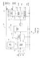
- FIG. 1is a block diagram of an example memory system compatible with certain embodiments described herein.
- FIG. 2is a block diagram of an example memory module with ECC (error-correcting code) having a volatile memory subsystem with nine volatile memory elements and a non-volatile memory subsystem with five non-volatile memory elements in accordance with certain embodiments described herein.
- ECCerror-correcting code
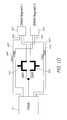
- FIG. 3is a block diagram of an example memory module having a microcontroller unit and logic element integrated into a single device in accordance with certain embodiments described herein.
- FIGS. 4A-4Cschematically illustrate example embodiments of memory systems having volatile memory subsystems comprising registered dual in-line memory modules in accordance with certain embodiments described herein.
- FIG. 5schematically illustrates an example power module of a memory system in accordance with certain embodiments described herein.
- FIG. 6is a flowchart of an example method of providing a first voltage and a second voltage to a memory system including volatile and non-volatile memory subsystems.
- FIG. 7is a flowchart of an example method of controlling a memory system operatively coupled to a host system and which includes at least 100 percent more storage capacity in non-volatile memory than in volatile memory.
- FIG. 8schematically illustrates an example clock distribution topology of a memory system in accordance with certain embodiments described herein.
- FIG. 9is a flowchart of an example method of controlling a memory system operatively coupled to a host system, the method including operating a volatile memory subsystem at a reduced rate in a back-up mode.
- FIG. 10schematically illustrates an example topology of a connection to transfer data slices from two DRAM segments of a volatile memory subsystem of a memory system to a controller of the memory system.
- FIG. 11is a flowchart of an example method of controlling a memory system operatively coupled to a host system, the method including backing up and/or restoring a volatile memory subsystem in slices.
- Certain embodiments described hereininclude a memory system which can communicate with a host system such as a disk controller of a computer system.
- the memory systemcan include volatile and non-volatile memory, and a controller.
- the controllerbacks up the volatile memory using the non-volatile memory in the event of a trigger condition.
- Trigger conditionscan include, for example, a power failure, power reduction, request by the host system, etc.
- the memory systemcan include a secondary power source which does not comprise a battery and may include, for example, a capacitor or capacitor array.
- the memory systemcan be configured such that the operation of the volatile memory is not adversely affected by the non-volatile memory or by the controller when the volatile memory is interacting with the host system.
- one or more isolation devicesmay isolate the non-volatile memory and the controller from the volatile memory when the volatile memory is interacting with the host system and may allow communication between the volatile memory and the non-volatile memory when the data of the volatile memory is being restored or backed-up. This configuration generally protects the operation of the volatile memory when isolated while providing backup and restore capability in the event of a trigger condition, such as a power failure.
- the memory systemincludes a power module which provides power to the various components of the memory system from different sources based on a state of the memory system in relation to a trigger condition (e.g., a power failure).
- the power modulemay switch the source of the power to the various components in order to efficiently provide power in the event of the power failure. For example, when no power failure is detected, the power module may provide power to certain components, such as the volatile memory, from system power while charging a secondary power source (e.g., a capacitor array). In the event of a power failure or other trigger condition, the power module may power the volatile memory elements using the previously charged secondary power source.
- the power moduletransitions relatively smoothly from powering the volatile memory with system power to powering it with the secondary power source.
- the power systemmay power volatile memory with a third power source from the time the memory system detects that power failure is likely to occur until the time the memory system detects that the power failure has actually occurred.
- the volatile memory systemcan be operated at a reduced frequency during backup and/or restore operations which can improve the efficiency of the system and save power.
- the volatile memorycommunicates with the non-volatile memory by writing and/or reading data words in bit-wise slices instead of by writing entire words at once.
- the unused slice(s) of volatile memoryis not active, which can reduce the power consumption of the system.
- the non-volatile memorycan include at least 100 percent more storage capacity than the volatile memory. This configuration can allow the memory system to efficiently handle subsequent trigger conditions.
- FIG. 1is a block diagram of an example memory system 10 compatible with certain embodiments described herein.
- the memory system 10can be coupled to a host computer system and can include a volatile memory subsystem 30 , a non-volatile memory subsystem 40 , and a controller 62 operatively coupled to the non-volatile memory subsystem 40 .
- the memory system 10includes at least one circuit 52 configured to selectively operatively decouple the controller 62 from the volatile memory subsystem 30 .
- the memory system 10comprises a memory module.
- the memory system 10may comprise a printed-circuit board (PCB) 20 .
- the memory system 10has a memory capacity of 512-MB, 1-GB, 2-GB, 4-GB, or 8-GB. Other volatile memory capacities are also compatible with certain embodiments described herein.
- the memory system 10has a non-volatile memory capacity of 512-MB, 1-GB, 2-GB, 4-GB, 8-GB, 16-GB, or 32-GB. Other non-volatile memory capacities are also compatible with certain embodiments described herein.
- the PCB 20has an industry-standard form factor.
- the PCB 20can have a low profile (LP) form factor with a height of 30 millimeters and a width of 133.35 millimeters.
- the PCB 20has a very high profile (VHP) form factor with a height of 50 millimeters or more.
- VLPvery low profile
- SO-DIMMsmall-outline
- UDIMMunbuffered
- RDIMMregistered (RDIMM)
- BFDIMMfully-buffered
- miniDIMMmini-RDIMM
- VLP mini-DIMMVLP mini-DIMM
- micro-DIMMmicro-DIMM
- SRAM DIMMsmall-outline
- certain non-DIMM form factorsare possible such as, for example, single in-line memory module (SIMM), multi-media card (MMC), and small computer system interface (SCSI).
- the memory system 10is in electrical communication with the host system. In other embodiments, the memory system 10 may communicate with a host system using some other type of communication, such as, for example, optical communication. Examples of host systems include, but are not limited to, blade servers, 1U servers, personal computers (PCs), and other applications in which space is constrained or limited.
- the memory system 10can be in communication with a disk controller of a computer system, for example.
- the PCB 20can comprise an interface 22 that is configured to be in electrical communication with the host system (not shown).
- the interface 22can comprise a plurality of edge connections which fit into a corresponding slot connector of the host system.
- the interface 22 of certain embodimentsprovides a conduit for power voltage as well as data, address, and control signals between the memory system 10 and the host system.
- the interface 22can comprise a standard 240-pin DDR2 edge connector.
- the volatile memory subsystem 30comprises a plurality of volatile memory elements 32 and the non-volatile memory subsystem 40 comprises a plurality of non-volatile memory elements 42 .
- Certain embodiments described hereinadvantageously provide non-volatile storage via the non-volatile memory subsystem 40 in addition to high-performance (e.g., high speed) storage via the volatile memory subsystem 30 .
- the first plurality of volatile memory elements 32comprises two or more dynamic random-access memory (DRAM) elements.
- DRAMdynamic random-access memory
- Types of DRAM elements 32 compatible with certain embodiments described hereininclude, but are not limited to, DDR, DDR2, DDR3, and synchronous DRAM (SDRAM). For example, in the block diagram of FIG.
- the first memory bank 30comprises eight 64Mx8 DDR2 SDRAM elements 32 .
- the volatile memory elements 32may comprise other types of memory elements such as static random-access memory (SRAM).
- volatile memory elements 32 having bit widths of 4, 8, 16, 32, as well as other bit widths,are compatible with certain embodiments described herein.
- Volatile memory elements 32 compatible with certain embodiments described hereinhave packaging which include, but are not limited to, thin small-outline package (TSOP), ball-grid-array (BGA), fine-pitch BGA (FBGA), micro-BGA (1.1,BGA), mini-BGA (mBGA), and chip-scale packaging (CSP).
- TSOPthin small-outline package
- BGAball-grid-array
- FBGAfine-pitch BGA
- micro-BGA1.1,BGA
- mini-BGAmini-BGA
- CSPchip-scale packaging
- the second plurality of non-volatile memory elements 42comprises one or more flash memory elements.
- Types of flash memory elements 42 compatible with certain embodiments described hereininclude, but are not limited to, NOR flash, NAND flash, ONE-NAND flash, and multi-level cell (MLC).
- MLCmulti-level cell
- the second memory bank 40comprises 512 MB of flash memory organized as four 128 Mbx8 NAND flash memory elements 42 .
- nonvolatile memory elements 42having bit widths of 4, 8, 16, 32, as well as other bit widths, are compatible with certain embodiments described herein.
- Non-volatile memory elements 42 compatible with certain embodiments described hereinhave packaging which include, but are not limited to, thin small-outline package (TSOP), ball-grid-array (BGA), fine-pitch BGA (FBGA), micro-BGA (PGA), mini-BGA (mBGA), and chip-scale packaging (CSP).
- TSOPthin small-outline package
- BGAball-grid-array
- FBGAfine-pitch BGA
- PGAmicro-BGA
- mini-BGAmini-BGA
- CSPchip-scale packaging
- FIG. 2is a block diagram of an example memory module 10 with ECC (error-correcting code) having a volatile memory subsystem 30 with nine volatile memory elements 32 and a non-volatile memory subsystem 40 with five non-volatile memory elements 42 in accordance with certain embodiments described herein.
- the additional memory element 32 of the first memory bank 30 and the additional memory element 42 of the second memory bank 40provide the ECC capability.
- the volatile memory subsystem 30comprises other numbers of volatile memory elements 32 (e.g., 2, 3, 4, 5, 6, 7, more than 9).
- the non-volatile memory subsystem 40comprises other numbers of non-volatile memory elements 42 (e.g., 2, 3, more than 5).
- the logic element 70comprises a field-programmable gate array (FPGA).
- the logic element 70comprises an FPGA available from Lattice Semiconductor Corporation which includes an internal flash.
- the logic element 70comprises an FPGA available from another vendor.
- the internal flashcan improve the speed of the memory system 10 and save physical space.
- Other types of logic elements 70 compatible with certain embodiments described hereininclude, but are not limited to, a programmable-logic device (PLD), an application-specific integrated circuit (ASIC), a custom-designed semiconductor device, a complex programmable logic device (CPLD).
- the logic element 70is a custom device.
- the logic element 70comprises various discrete electrical elements, while in certain other embodiments, the logic element 70 comprises one or more integrated circuits.
- FIG. 3is a block diagram of an example memory module 10 having a microcontroller unit 60 and logic element 70 integrated into a single controller 62 in accordance with certain embodiments described herein.
- the controller 62includes one or more other components. For example, in one embodiment, an FPGA without an internal flash is used and the controller 62 includes a separate flash memory component which stores configuration information to program the FPGA.
- the at least one circuit 52comprises one or more switches coupled to the volatile memory subsystem 30 , to the controller 62 , and to the host computer (e.g., via the interface 22 , as schematically illustrated by FIGS. 1-3 ).
- the one or more switchesare responsive to signals (e.g., from the controller 62 ) to selectively operatively decouple the controller 62 from the volatile memory subsystem 30 and to selectively operatively couple the controller 62 to the volatile memory subsystem 30 .
- the at least one circuit 52selectively operatively couples and decouples the volatile memory subsystem 30 and the host system.
- the volatile memory subsystem 30can comprise a registered DIMM subsystem comprising one or more registers 160 and a plurality of DRAM elements 180 , as schematically illustrated by FIG. 4A .
- the at least one circuit 52can comprise one or more switches 172 coupled to the controller 62 (e.g., logic element 70 ) and to the volatile memory subsystem 30 which can be actuated to couple and decouple the controller 62 to and from the volatile memory subsystem 30 , respectively.
- the memory system 10further comprises one or more switches 170 coupled to the one or more registers 160 and to the plurality of DRAM elements 180 as schematically illustrated by FIG. 4A .
- the one or more switches 170can be selectively switched, thereby selectively operatively coupling the volatile memory subsystem 30 to the host system 150 .
- the one or more switches 174are also coupled to the one or more registers 160 and to a power source 162 for the one or more registers 160 .
- the one or more switches 174can be selectively switched to turn power on or off to the one or more registers 160 , thereby selectively operatively coupling the volatile memory subsystem 30 to the host system 150 .
- the at least one circuit 52comprises a dynamic on-die termination (ODT) 176 circuit of the logic element 70 .
- ODTdynamic on-die termination
- the logic element 70can comprise a dynamic ODT circuit 176 which selectively operatively couples and decouples the logic element 70 to and from the volatile memory subsystem 30 , respectively.
- the one or more switches 170can be selectively switched, thereby selectively operatively coupling the volatile memory subsystem 30 to the host system 150 .
- the non-volatile memory subsystem 40may backup the volatile memory subsystem 30 in the event of a trigger condition, such as, for example, a power failure or power reduction or a request from the host system.
- a trigger conditionsuch as, for example, a power failure or power reduction or a request from the host system.
- the non-volatile memory subsystem 40holds intermediate data results in a noisy system environment when the host computer system is engaged in a long computation.
- a backupmay be performed on a regular basis. For example, in one embodiment, the backup may occur every millisecond in response to a trigger condition.
- the trigger conditionoccurs when the memory system 10 detects that the system voltage is below a certain threshold voltage.
- the threshold voltageis 10 percent below a specified operating voltage.
- a trigger conditionoccurs when the voltage goes above a certain threshold value, such as, for example, 10 percent above a specified operating voltage.
- a trigger conditionoccurs when the voltage goes below a threshold or above another threshold.
- a backup and/or restore operationmay occur in reboot and/or non-reboot trigger conditions.
- the controller 62may comprise a microcontroller unit (MCU) 60 and a logic element 70 .
- the MCU 60provides memory management for the non-volatile memory subsystem 40 and controls data transfer between the volatile memory subsystem 30 and the non-volatile memory subsystem 40 .
- the MCU 60 of certain embodimentscomprises a 16-bit microcontroller, although other types of microcontrollers are also compatible with certain embodiments described herein.
- the logic element 70 of certain embodimentsis in electrical communication with the non-volatile memory subsystem 40 and the MCU 60 .
- the logic element 70can provide signal level translation between the volatile memory elements 32 (e.g., 1.8V SSTL-2 for DDR2 SDRAM elements) and the non-volatile memory elements 42 (e.g., 3V TTL for NAND flash memory elements). In certain embodiments, the logic element 70 is also programmed to perform address/address translation between the volatile memory subsystem 30 and the non-volatile memory subsystem 40 . In certain preferred embodiments, 1-NAND type flash are used for the non-volatile memory elements 42 because of their superior read speed and compact structure.
- the memory system 10 of certain embodimentsis configured to be operated in at least two states.
- the at least two statescan comprise a first state in which the controller 62 and the non-volatile memory subsystem 40 are operatively decoupled (e.g., isolated) from the volatile memory subsystem 30 by the at least one circuit 52 and a second state in which the volatile memory subsystem 30 is operatively coupled to the controller 62 to allow data to be communicated between the volatile memory subsystem 30 and the nonvolatile memory subsystem 40 via the controller 62 .
- the memory system 10may transition from the first state to the second state in response to a trigger condition, such as when the memory system 10 detects that there is a power interruption (e.g., power failure or reduction) or a system hang-up.
- a power interruptione.g., power failure or reduction
- the memory system 10may further comprise a voltage monitor 50 .
- the voltage monitor circuit 50monitors the voltage supplied by the host system via the interface 22 .
- the voltage monitor circuit 50may transmit a signal to the controller 62 indicative of the detected condition.
- the controller 62responds to the signal from the voltage monitor circuit 50 by transmitting a signal to the at least one circuit 52 to operatively couple the controller to the volatile memory system 30 , such that the memory system 10 enters the second state.
- the voltage monitor 50may send a signal to the MCU 60 which responds by accessing the data on the volatile memory system 30 and by executing a write cycle on the non-volatile memory subsystem 40 .
- the voltage monitor circuit 50is part of the controller 62 (e.g., part of the MCU 60 ) and the voltage monitor circuit 50 transmits a signal to the other portions of the controller 62 upon detecting a power threshold condition.
- the isolation or operational decoupling of the volatile memory subsystem 30 from the non-volatile memory subsystem in the first statecan preserve the integrity of the operation of the memory system 10 during periods of operation in which signals (e.g., data) are transmitted between the host system and the volatile memory subsystem 30 .
- the controller 62 and the nonvolatile memory subsystem 40do not add a significant capacitive load to the volatile memory system 30 when the memory system 10 is in the first state.
- the capacitive load of the controller 62 and the non-volatile memory subsystem 40do not significantly affect the signals propagating between the volatile memory subsystem 30 and the host system. This can be particularly advantageous in relatively high-speed memory systems where loading effects can be significant.
- the at least one circuit 52comprises an FSA 1208 Low-Power, Eight-Port, Hi-Speed Isolation Switch from Fairchild Semiconductor. In other embodiments, the at least one circuit 52 comprises other types of isolation devices.
- Powermay be supplied to the volatile memory subsystem 30 from a first power supply (e.g., a system power supply) when the memory system 10 is in the first state and from a second power supply 80 when the memory system 10 is in the second state.
- the memory system 10is in the first state when no trigger condition (e.g., a power failure) is present and the memory system 10 enters the second state in response to a trigger condition.
- the memory system 10has a third state in which the controller 62 is operatively decoupled from the volatile memory subsystem 30 and power is supplied to the volatile memory subsystem 30 from a third power supply (not shown).
- the third power supplymay provide power to the volatile memory subsystem 30 when the memory system 10 detects that a trigger condition is likely to occur but has not yet occurred.
- the second power supply 80does not comprise a battery. Because a battery is not used, the second power supply 80 of certain embodiments may be relatively easy to maintain, does not generally need to be replaced, and is relatively environmentally friendly.
- the second power supply 80comprises a step-up transformer 82 , a step-down transformer 84 , and a capacitor bank 86 comprising one or more capacitors (e.g., double-layer capacitors).
- capacitorsmay take about three to four minutes to charge and about two minutes to discharge. In other embodiments, the one or more capacitors may take a longer time or a shorter time to charge and/or discharge.
- the second power supply 80is configured to power the volatile memory subsystem 30 for less than thirty minutes.
- the second power supply 80may comprise a battery.
- the second power supply 80comprises a battery and one or more capacitors and is configured to power the volatile memory subsystem 30 for no more than thirty minutes.
- the capacitor bank 86 of the second power supply 80is charged by the first power supply while the memory system 10 is in the first state. As a result, the second power supply 80 is fully charged when the memory system 10 enters the second state.
- the memory system 10 and the second power supply 80may be located on the same printed circuit board 20 . In other embodiments, the second power supply 80 may not be on the same printed circuit board 20 and may be tethered to the printed circuit board 20 , for example.
- the step-up transformer 82keeps the capacitor bank 86 charged at a peak value.
- the step-down transformer 84acts as a voltage regulator to ensure that regulated voltages are supplied to the memory elements (e.g., 1.8V to the volatile DRAM elements 32 and 3.0V to the non-volatile flash memory elements 42 ) when operating in the second state (e.g., during power down).
- the memory elementse.g., 1.8V to the volatile DRAM elements 32 and 3.0V to the non-volatile flash memory elements 42
- the second statee.g., during power down.
- the memory module 10further comprises a switch 90 (e.g., FET switch) that switches power provided to the controller 62 , the volatile memory subsystem 30 , and the non-volatile memory subsystem 40 , between the power from the second power supply 80 and the power from the first power supply (e.g., system power) received via the interface 22 .
- the switch 90may switch from the first power supply to the second power supply 80 when the voltage monitor 50 detects a low voltage condition.
- the switch 90 of certain embodimentsadvantageously ensures that the volatile memory elements 32 and non-volatile memory elements 42 are powered long enough for the data to be transferred from the volatile memory elements 32 and stored in the non-volatile memory elements 42 .
- the switch 90then switches back to the first power supply and the controller 62 transmits a signal to the at least one circuit 52 to operatively decouple the controller 62 from the volatile memory subsystem 30 , such that the memory system 10 reenters the first state.
- datamay be transferred back from the non-volatile memory subsystem 40 to the volatile memory subsystem 30 via the controller 62 .
- the host systemcan then resume accessing the volatile memory subsystem 30 of the memory module 10 .
- the host systemaccesses the volatile memory subsystem 30 rather than the non-volatile memory subsystem 40 because the volatile memory elements 32 have superior read/write characteristics.
- the transfer of data from the volatile memory bank 30 to the nonvolatile memory bank 40 , or from the non-volatile memory bank 40 to the volatile memory bank 30takes less than one minute per GB.
- the memory system 10protects the operation of the volatile memory when communicating with the host-system and provides backup and restore capability in the event of a trigger condition such as a power failure. In certain embodiments, the memory system 10 copies the entire contents of the volatile memory subsystem 30 into the non-volatile memory subsystem 40 on each backup operation. Moreover, in certain embodiments, the entire contents of the non-volatile memory subsystem 40 are copied back into the volatile memory subsystem 30 on each restore operation.
- the entire contents of the non-volatile memory subsystem 40are accessed for each backup and/or restore operation, such that the non-volatile memory subsystem 40 (e.g., flash memory subsystem) is used generally uniformly across its memory space and wear-leveling is not performed by the memory system 10 . In certain embodiments, avoiding wear-leveling can decrease cost and complexity of the memory system 10 and can improve the performance of the memory system 10 . In certain other embodiments, the entire contents of the volatile memory subsystem 30 are not copied into the non-volatile memory subsystem 40 on each backup operation, but only a partial copy is performed. In certain embodiments, other management capabilities such as bad-block management and error management for the flash memory elements of the non-volatile memory subsystem 40 are performed in the controller 62 .
- the non-volatile memory subsystem 40e.g., flash memory subsystem
- the memory system 10generally operates as a write-back cache in certain embodiments.
- the host systeme.g., a disk controller
- writes data to the volatile memory subsystem 30which then writes the data to non-volatile storage which is not part of the memory system 10 , such as, for example, a hard disk.
- the disk controllermay wait for an acknowledgment signal from the memory system 10 indicating that the data has been written to the hard disk or is otherwise secure.
- the memory system 10 of certain embodimentscan decrease delays in the system operation by indicating that the data has been written to the hard disk before it has actually done so.
- the memory system 10will still be able to recover the data efficiently in the event of a power outage because of the backup and restore capabilities described herein.
- the memory system 10may be operated as a write-through cache or as some other type of cache.
- FIG. 5schematically illustrates an example power module 100 of the memory system 10 in accordance with certain embodiments described herein.
- the power module 100provides power to the various components of the memory system 10 using different elements based on a state of the memory system 10 in relation to a trigger condition.
- the power module 100comprises one or more of the components described above with respect to FIG. 1 .
- the power module 100includes the second power supply 80 and the switch 90 .
- the power module 100provides a plurality of voltages to the memory system 10 comprising non-volatile and volatile memory subsystems 30 , 40 .
- the plurality of voltagescomprises at least a first voltage 102 and a second voltage 104 .
- the power module 100comprises an input 106 providing a third voltage 108 to the power module 100 and a voltage conversion element 120 configured to provide the second voltage 104 to the memory system 10 .
- the power module 100further comprises a first power element 130 configured to selectively provide a fourth voltage 110 to the conversion element 120 .
- the first power element 130comprises a pulse-width modulation power controller.
- the first power element 130is configured to receive a 1.8V input system voltage as the third voltage 108 and to output a modulated 5V output as the fourth voltage 110 .
- the power module 100further comprises a second power element 140 can be configured to selectively provide a fifth voltage 112 to the conversion element 120 .
- the power module 100can be configured to selectively provide the first voltage 102 to the memory system 10 either from the conversion element 120 or from the input 106 .
- the power module 100can be configured to be operated in at least three states in certain embodiments.
- a first statethe first voltage 102 is provided to the memory system 10 from the input 106 and the fourth voltage 110 is provided to the conversion element 120 from the first power element 130 .
- the fourth voltage 110is provided to the conversion element 120 from the first power element 130 and the first voltage 102 is provided to the memory system 10 from the conversion element 120 .
- the fifth voltage 112is provided to the conversion element 120 from the second power element 140 and the first voltage 104 is provided to the memory system 10 from the conversion element 120 .
- the power module 100transitions from the first state to the second state upon detecting that a trigger condition is likely to occur and transitions from the second state to the third state upon detecting that the trigger condition has occurred. For example, the power module 100 may transition to the second state when it detects that a power failure is about to occur and transitions to the third state when it detects that the power failure has occurred.
- providing the first voltage 102 in the second state from the first power element 130 rather than from the input 106allows a smoother transition from the first state to the third state. For example, in certain embodiments, providing the first voltage 102 from the first power element 130 has capacitive and other smoothing effects.
- switching the point of power transition to be between the conversion element 120 and the first and second power elements 130 , 140can smooth out potential voltage spikes.
- the second power element 140does not comprise a battery and may comprise one or more capacitors.
- the second power element 140comprises a capacitor array 142 , a buck-boost converter 144 which adjusts the voltage for charging the capacitor array and a voltage/current limiter 146 which limits the charge current to the capacitor array 142 and stops charging the capacitor array 142 when it has reached a certain charge voltage.
- the capacitor array 142comprises two 50 farad capacitors capable of holding a total charge of 4.6V.
- the buck-boost converter 144receives a 1.8V system voltage (first voltage 108 ) and boosts the voltage to 4.3V which is outputted to the voltage current limiter 146 .
- the voltage/current limiter 146limits the current going to the capacitor array 142 to 1 A and stops charging the array 142 when it is charged to 4.3V.
- the second power element 140may include alternative embodiments. For example, different components and/or different value components may be used.
- a pure boost convertermay be used instead of a buck-boost converter.
- only one capacitormay be used instead of a capacitor array 142 .
- the conversion element 120can comprise one or more buck converters and/or one or more buck-boost converters.
- the conversion element 120may comprise a plurality of sub-blocks 122 , 124 , 126 as schematically illustrated by FIG. 4 , which can provide more voltages in addition to the second voltage 104 to the memory system 10 .
- the sub-blocksmay comprise various converter circuits such as buck-converters, boost converters, and buck-boost converter circuits for providing various voltage values to the memory system 10 .
- sub-block 122comprises a buck converter
- sub-block 124comprises a dual buck converter
- sub-block 126comprises a buck-boost converter as schematically illustrated by FIG. 4 .
- the conversion element 120receives as input either the fourth voltage 110 from the first power element 130 or the fifth voltage 112 from the second power element 140 , depending on the state of the power module 100 , and reduces the input to an appropriate amount for powering various components of the memory system.
- the buck-converter of sub-block 122can provide 1.8V at 2 A for about 60 seconds to the volatile memory elements 32 (e.g., DRAM), the non-volatile memory elements 42 (e.g., flash), and the controller 62 (e.g., an FPGA) in one embodiment.
- the sub-block 124can provide the second voltage 104 as well as another reduced voltage 105 to the memory system 10 .
- the second voltage 104is 2.5V and is used to power the at least one circuit 52 (e.g., isolation device) and the other reduced voltage 105 is 1.2V and is used to power the controller 62 (e.g., FPGA).
- the sub-block 126can provide yet another voltage 107 to the memory system 10 .
- the voltage 107may be 3.3V and may be used to power both the controller 62 and the at least one circuit 52 .
- the conversion element 120may include alternative embodiments.
- the volatile memory elements 32 and nonvolatile memory elements 42are powered using independent voltages and are not both powered using the first voltage 102 .
- FIG. 6is a flowchart of an example method 200 of providing a first voltage 102 and a second voltage 104 to a memory system 10 including volatile and nonvolatile memory subsystems 30 , 40 . While the method 200 is described herein by reference to the memory system 10 schematically illustrated by FIGS. 1-4 , other memory systems are also compatible with embodiments of the method 200 .
- the method 200comprises providing the first voltage 102 to the memory system 10 from an input power supply 106 and providing the second voltage 104 to the memory system 10 from a first power subsystem in operational block 210 .
- the first power subsystemcomprises the first power element 130 and the voltage conversion element 120 described above with respect to FIG. 4 . In other embodiments, other first power subsystems are used.
- the method 200further comprises detecting a second condition in operational block 220 .
- detecting the second conditioncomprises detecting that a trigger condition is likely to occur.
- the method 200comprises providing the first voltage 102 and the second voltage 104 to the memory system 10 from the first power subsystem in an operational block 230 .
- a switch 148can be toggled to provide the first voltage 102 from the conversion element 120 rather than from the input power supply.
- the method 200further comprises charging a second power subsystem in operational block 240 .
- the second power subsystemcomprises the second power element 140 or another power supply that does not comprise a battery.
- the second power subsystemcomprises the second power element 140 and the voltage conversion element 120 described above with respect to FIG. 4 . In other embodiments, some other second power subsystem is used.
- the method 200further comprises detecting a third condition in an operational block 250 and during the third condition, providing the first voltage 102 and the second voltage 104 to the memory system 10 from the second power subsystem 140 in an operational block 250 .
- detecting the third conditioncomprises detecting that the trigger condition has occurred.
- the trigger conditionmay comprise various conditions described herein.
- the trigger conditioncomprises a power reduction, power failure, or system hang-up.
- the operational blocks of the method 200may be performed in different orders in various embodiments. For example, in certain embodiments, the second power subsystem 140 is charged before detecting the second condition.
- the memory system 10comprises a volatile memory subsystem 30 and a non-volatile memory subsystem 40 comprising at least 100 percent more storage capacity than does the volatile memory subsystem.
- the memory system 10also comprises a controller 62 operatively coupled to the volatile memory subsystem 30 and operatively coupled to the non-volatile memory subsystem 40 .
- the controller 62can be configured to allow data to be communicated between the volatile memory subsystem 30 and the host system when the memory system 10 is operating in a first state and to allow data to be communicated between the volatile memory subsystem 30 and the non-volatile memory subsystem 40 when the memory system 10 is operating in a second state.
- the memory system 10 having extra storage capacity of the non-volatile memory subsystem 40has been described with respect to certain embodiments, alternative configurations exist. For example, in certain embodiments, there may be more than 100 percent more storage capacity in the non-volatile memory subsystem 40 than in the volatile memory subsystem 30 . In various embodiments, there may be at least 200, 300, or 400 percent more storage capacity in the non-volatile memory subsystem 40 than in the volatile memory subsystem 30 . In other embodiments, the non-volatile memory subsystem 40 includes at least some other integer multiples of the storage capacity of the volatile memory subsystem 30 . In some embodiments, the non-volatile memory subsystem 40 includes a non-integer multiple of the storage capacity of the volatile memory subsystem 30 . In one embodiment, the non-volatile memory subsystem 40 includes less than 100 percent more storage capacity than does the volatile memory subsystem 30 .
- the extra storage capacity of the non-volatile memory subsystem 40can be used to improve the backup capability of the memory system 10 .
- the extra storage capacity of the non-volatile memory subsystem 40allows the volatile memory subsystem 30 to be backed up in the event of a subsequent power failure or other trigger event.
- the extra storage capacity of the non-volatile memory subsystem 40may allow the memory system 10 to backup the volatile memory subsystem 30 efficiently in the event of multiple trigger conditions (e.g., power failures).
- the data in the volatile memory system 30is copied to a first, previously erased portion of the nonvolatile memory subsystem 40 via the controller 62 . Since the non-volatile memory subsystem 40 has more storage capacity than does the volatile memory subsystem 30 , there is a second portion of the non-volatile memory subsystem 40 which does not have data from the volatile memory subsystem 30 copied to it and which remains free of data (e.g., erased).
- the controller 62 of the memory system 10restores the data to the volatile memory subsystem 30 by copying the backed-up data from the non-volatile memory subsystem 40 back to the volatile memory subsystem 30 . After the data is restored, the memory system 10 erases the non-volatile memory subsystem 40 . While the first portion of the non-volatile memory subsystem 40 is being erased, it may be temporarily unaccessible.
- the volatile memory subsystem 30can be backed-up or stored again in the second portion of the non-volatile memory subsystem 40 as described herein.
- the extra storage capacity of the non-volatile memory subsystem 40may allow the memory system 10 to operate more efficiently. For example, because of the extra storage capacity of the non-volatile memory subsystem 40 , the memory system 10 can handle a higher frequency of trigger events that is not limited by the erase time of the non-volatile memory subsystem 40 .
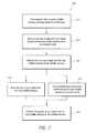
- FIG. 7is a flowchart of an example method 300 of controlling a memory system 10 operatively coupled to a host system and which includes a volatile memory subsystem 30 and a non-volatile memory subsystem 40 .
- the non-volatile memory subsystem 40comprises at least 100 percent more storage capacity than does the volatile memory subsystem 30 as described herein. While the method 300 is described herein by reference to the memory system 10 schematically illustrated by FIGS. 1-3 , the method 300 can be practiced using other memory systems in accordance with certain embodiments described herein.
- the method 300comprises communicating data between the volatile memory subsystem 30 and the host system when the memory system 10 is in a first mode of operation.
- the method 300further comprises storing a first copy of data from the volatile memory subsystem 30 to the non-volatile memory subsystem 40 at a first time when the memory system 10 is in a second mode of operation in an operational block 320 .
- the method 300comprises restoring the first copy of data from the non-volatile memory subsystem 40 to the volatile memory subsystem 30 .
- the method 300further comprises erasing the first copy of data from the non-volatile memory subsystem 40 in an operational block 340 .
- the methodfurther comprises storing a second copy of data from the volatile memory subsystem 30 to the non-volatile memory subsystem 40 at a second time when the memory system 10 is in the second mode of operation in an operational block 350 . Storing the second copy begins before the first copy is completely erased from the non-volatile memory subsystem 40 .
- the memory system 10enters the second mode of operation in response to a trigger condition, such as a power failure.
- a trigger conditionsuch as a power failure.
- the first copy of data and the second copy of dataare stored in separate portions of the nonvolatile memory subsystem 40 .
- the method 300can also include restoring the second copy of data from the non-volatile memory subsystem 40 to the volatile memory subsystem 30 in an operational block 360 .
- the operational blocks of method 300 referred to hereinmay be performed in different orders in various embodiments. For example, in some embodiments, the second copy of data is restored to the volatile memory subsystem 30 at operational block 360 before the first copy of data is completely erased in the operational block 340 .
- FIG. 8schematically illustrates an example clock distribution topology 400 of a memory system 10 in accordance with certain embodiments described herein.
- the clock distribution topology 400generally illustrates the creation and routing of the clock signals provided to the various components of the memory system 10 .
- a clock source 402such as, for example, a 25 MHz oscillator, generates a clock signal.
- the clock source 402may feed a clock generator 404 which provides a clock signal 406 to the controller 62 , which may be an FPGA.
- the clock generator 404generates a 125 MHz clock signal 406 .
- the controller 62receives the clock signal 406 and uses it to clock the controller 62 master state control logic.
- the master state control logicmay control the general operation of an FPGA controller 62 .
- the clock signal 406can also be input into a clock divider 410 which produces a frequency-divided version of the clock signal 406 .
- the clock divider 410is a divide by two clock divider and produces a 62.5 MHz clock signal in response to the 125 MHz clock signal 406 .
- a non-volatile memory phase-locked loop (PLL) block 412can be included (e.g., in the controller 62 ) which distributes a series of clock signals to the non-volatile memory subsystem 40 and to associated control logic.
- a series of clock signals 414can be sent from the controller 62 to the non-volatile memory subsystem 40 .
- Another clock signal 416can be used by the controller logic which is dedicated to controlling the non-volatile memory subsystem 40 .
- the clock signal 416may clock the portion of the controller 62 which is dedicated to generating address and/or control lines for the non-volatile memory subsystem 40 .
- a feedback clock signal 418is fed back into the non-volatile memory PLL block 412 .
- the PLL block 412compares the feedback clock 418 to the reference clock 411 and varies the phase and frequency of its output until the reference 411 and feedback 418 clocks are phase and frequency matched.
- a version of the clock signal 406 such as the backup clock signal 408may be sent from the controller to the volatile memory subsystem 30 .
- the clock signal 408may be, for example, a differential version of the clock signal 406 .
- the backup clock signal 408may be used to clock the volatile memory subsystem 30 when the memory system 10 is backing up the data from the volatile memory subsystem 30 into the non-volatile memory subsystem 40 .
- the backup clock signal 408may also be used to clock the volatile memory subsystem 30 when the memory system 10 is copying the backed-up data back into the volatile memory subsystem 30 from the nonvolatile memory subsystem 40 (also referred to as restoring the volatile memory subsystem 30 ).
- the volatile memory subsystem 30may normally be run at a higher frequency (e.g., DRAM running at 400 MHz) than the non-volatile memory subsystem 40 (e.g., flash memory running at 62.5 MHz) when communicating with the host system (e.g., when no trigger condition is present). However, in certain embodiments the volatile memory subsystem 30 may be operated at a reduced frequency (e.g., at twice the frequency of the non-volatile memory subsystem 40 ) without introducing significant delay into the system during backup operation and/or restore operations. Running the volatile memory subsystem 30 at the reduced frequency during a backup and/or restore operation may advantageously reduce overall power consumption of the memory system 10 .
- a reduced frequencye.g., at twice the frequency of the non-volatile memory subsystem 40
- the backup clock 408 and the volatile memory system clock signal 420are received by a multiplexer 422 , as schematically illustrated by FIG. 8 .
- the multiplexer 422can output either the volatile memory system clock signal 420 or the backup clock signal 408 depending on the backup state of the memory system 10 .
- the volatile memory system clock signal 420may be provided by the multiplexer 422 to the volatile memory PLL block 424 .
- the backup clock signal 408may be provided.
- the volatile memory PLL block 424receives the volatile memory reference clock signal 423 from the multiplexer 422 and can generate a series of clock signals which are distributed to the volatile memory subsystem 30 and associated control logic. For example, in one embodiment, the PLL block 424 generates a series of clock signals 426 which clock the volatile memory elements 32 . A clock signal 428 may be used to clock control logic associated with the volatile memory elements, such as one or more registers (e.g., the one ore more registers of a registered DIMM). Another clock signal 430 may be sent to the controller 62 . A feedback clock signal 432 is fed back into the volatile memory PLL block 424 . In one embodiment, the PLL block 424 compares the feedback clock signal 432 to the reference clock signal 423 and varies the phase and frequency of its output until the reference clock signal 423 and the feedback clock signal 432 clocks are phase and frequency matched.
- the clock signal 430may be used by the controller 62 to generate and distribute clock signals which will be used by controller logic which is configured to control the volatile memory subsystem 30 .
- control logic in the controller 62may be used to control the volatile memory subsystem 30 during a backup or restore operation.
- the clock signal 430may be used as a reference clock signal for the PLL block 434 which can generate one or more clocks 438 used by logic in the controller 62 .
- the PLL block 434may generate one or more clock signals 438 used to drive logic circuitry associated with controlling the volatile memory subsystem 30 .
- the PLL block 434includes a feedback clock signal 436 and operates in a similar manner to other PLL blocks described herein.
- the clock signal 430may be used as a reference clock signal for the PLL block 440 which may generate one or more clock signals used by a sub-block 442 to generate one or more other clock signals 444 .
- the volatile memory subsystem 30comprises DDR2 SDRAM elements and the sub-block 442 generates one or more DDR2 compatible clock signals 444 .
- a feedback clock signal 446is fed back into the PLL block 440 .
- the PLL block 440operates in a similar manner to other PLL blocks described herein.
- one or more of the clock signalshave a different frequency in various other embodiments.
- one or more of the clocks shown as differential signalsare single ended signals.
- the volatile memory subsystem 30operates on the volatile memory clock signal 420 and there is no backup clock signal 408 .
- the volatile memory subsystem 30is operated at a reduced frequency during a backup operation and not during a restore operation. In other embodiments, the volatile memory subsystem 30 is operated at a reduced frequency during a restore operation and not during a backup operation.
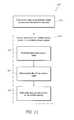
- FIG. 9is a flowchart of an example method 500 of controlling a memory system 10 operatively coupled to a host system. Although described with respect to the memory system 10 described herein, the method 500 is compatible with other memory systems.
- the memory system 10may include a clock distribution topology 400 similar to the one described above with respect to FIG. 8 or another clock distribution topology.
- the memory system 10can include a volatile memory subsystem 30 and a non-volatile memory subsystem 40 .
- the method 500comprises operating the volatile memory subsystem 30 at a first frequency when the memory system 10 is in a first mode of operation in which data is communicated between the volatile memory subsystem 30 and the host system.
- the method 500comprises operating the non-volatile memory subsystem 40 at a second frequency when the memory system 10 is in a second mode of operation in which data is communicated between the volatile memory subsystem 30 and the non-volatile memory subsystem 40 .
- the method 500further comprises operating the volatile memory subsystem 30 at a third frequency in an operational block 530 when the memory system 10 is in the second mode of operation.
- the memory system 10is not powered by a battery when it is in the second mode of operation.
- the memory system 10may switch from the first mode of operation to the second mode of operation in response to a trigger condition.
- the trigger conditionmay be any trigger condition described herein such as, for example, a power failure condition.
- the second mode of operationincludes both backup and restore operations as described herein.
- the second mode of operationincludes backup operations but not restore operations.
- the second mode of operationincludes restore operations but not backup operations.
- the third frequencycan be less than the first frequency.
- the third frequencycan be approximately equal to the second frequency.
- the reduced frequency operationis an optional mode.
- the first, second and/or third frequenciesare configurable by a user or by the memory system 10 .
- FIG. 10schematically illustrates an example topology of a connection to transfer data slices from two DRAM segments 630 , 640 of a volatile memory subsystem 30 of a memory system 10 to a controller 62 of the memory system 10 . While the example of FIG. 10 shows a topology including two DRAM segments 630 , 640 for the purposes of illustration, each address location of the volatile memory subsystem 30 comprises more than the two segments in certain embodiments.
- the data lines 632 , 642 from the first DRAM segment 630 and the second DRAM segment 640 of the volatile memory subsystem 30are coupled to switches 650 , 652 which are coupled to the controller 62 (e.g., logic element 70 ) of the memory system 10 .
- the chip select lines 634 , 644 and the self-refresh lines 636 , 646 (e.g., CKe signals) of the first and second DRAM segments 630 , 640 , respectively,are coupled to the controller 62 .
- the controller 62comprises a buffer (not shown) which is configured to store data from the volatile memory subsystem 30 .
- the bufferis a first-in, first out buffer (FIFO).
- data slices from each DRAM segment 630 , 640comprise a portion of the volatile memory subsystem data bus.
- the volatile memory subsystem 30comprises a 72-bit data bus (e.g., each data word at each addressable location is 72 bits wide and includes, for example, 64 bits of accessible SDRAM and 8 bits of ECC), the first data slice from the first DRAM segment 630 may comprise 40 bits of the data word, and the second data slice from the second DRAM segment 640 may comprise the remaining 32 bits of the data word.
- Certain other embodimentscomprise data buses and/or data slices of different sizes.
- the switches 650 , 652can each be selectively switched to selectively operatively couple the data lines 632 , 642 , respectively from the first and second DRAM segments 630 , 640 to the controller 62 .
- the chip select lines 634 , 644enable the first and second DRAM segments 630 , 640 , respectively, of the volatile memory subsystem 30 , and the self-refresh lines 636 , 646 toggle the first and second DRAM segments 630 , 640 , respectively, from self-refresh mode to active mode.
- the first and second DRAM segments 630 , 640maintain stored information but are not accessible when they are in self-refresh mode, and maintain stored information and are accessible when they are in active mode.
- data slices from only one of the two DRAM segments 630 , 640 at a timeare sent to the controller 62 .
- the controller 62sends a signal via the CKe line 636 to the first DRAM segment 630 to put the first DRAM segment 630 in active mode.
- the data slice from the first DRAM segment 630 for multiple wordsis written to the controller 62 before writing the second data slice from the second DRAM segment 640 to the controller 62 .
- the controller 62While the first data slice is being written to the controller 62 , the controller 62 also sends a signal via the CKe line 646 to put the second DRAM segment 640 in self-refresh mode.
- the controller 62puts the first DRAM segment 630 into self-refresh mode by sending a signal via the CKe line 636 to the first DRAM segment 640 .
- the controller 62also puts the second DRAM segment 640 into active mode by sending a signal via the CKe line 646 to the DRAM segment 640 .
- the second slice for a word or for a block of wordsis written to the controller 62 .
- the controller 62when the first and second data slices are written to the buffer in the controller 62 , the controller 62 combines the first and second data slices 630 , 640 into complete words or blocks of words and then writes each complete word or block of words to the non-volatile memory subsystem 40 . In certain embodiments, this process is called “slicing” the volatile memory subsystem 30 .
- the datamay be sliced in a restore operation as well as, or instead of, during a backup operation.
- the nonvolatile memory elements 42write each backed-up data word to the controller 62 which writes a first slice of the data word to the volatile memory subsystem 30 and then a second slice of the data word to the volatile memory subsystem 30 .
- slicing the volatile memory subsystem 30 during a restore operationmay be performed in a manner generally inverse to slicing the volatile memory subsystem 30 during a backup operation.
- FIG. 11is a flowchart of an example method 600 of controlling a memory system 10 operatively coupled to a host system and which includes a volatile memory subsystem 30 and a non-volatile memory subsystem 40 .
- the method 600comprises communicating data words between the volatile memory subsystem 30 and the host system when the memory system 10 is in a first mode of operation in an operational block 610 .
- the memory system 10may be in the first mode of operation when no trigger condition has occurred and the memory system is not performing a backup and/or restore operation or is not being powered by a secondary power supply.
- the methodfurther comprises transferring data words from the volatile memory subsystem 30 to the non-volatile memory subsystem 40 when the memory system 10 is in a second mode of operation.
- each data wordcomprises the data stored in a particular address of the memory system 10 .
- the memory system 10may enter the second mode of operation, for example, when a trigger condition (e.g., a power failure) occurs.
- transferring each data wordcomprises storing a first portion (also referred to as a slice) of the data word in a buffer in an operational block 622 , storing a second portion of the data word in the buffer in an operational block 624 , and writing the entire data word from the buffer to the non-volatile memory subsystem 40 in an operational block 626 .
- the data wordmay be a 72 bit data word (e.g., 64 bits of accessible SDRAM and 8 bits of ECC), the first portion (or “slice”) may comprise 40 bits of the data word, and the second portion (or “slice”) may comprise the remaining 32 bits of the data word.
- the bufferis included in the controller 62 .
- the bufferis a first-in, first-out buffer implemented in the controller 62 which comprises an FPGA.
- the method 600may generally be referred to as “slicing” the volatile memory during a backup operation.
- the process of “slicing” the volatile memory during a backupincludes bringing the 32-bit slice out of self-refresh, reading a 32-bit block from the slice into the buffer, and putting the 32-bit slice back into self-refresh.
- the 40-bit sliceis then brought out of self-refresh and a 40-bit block from the slice is read into a buffer.
- Each blockmay comprise a portion of multiple words.
- each 32-bit blockmay comprise 32-bit portions of multiple 72-bit words.
- each blockcomprises a portion of a single word.
- the 40-bit sliceis then put back into self-refresh in the example embodiment.
- the 32-bit and 40-bit slicesare then combined into a 72-bit block by the controller 62 and ECC detection/correction is performed on each 72-bit word as it is read from the buffer and written into the non-volatile memory subsystem (e.g., flash).
- the non-volatile memory subsysteme.g., flash
- the entire data wordmay comprise more than two portions.
- the entire data wordmay comprise three portions instead of two and transferring each data word further comprises storing a third portion of each data word in the buffer.
- the data wordmay comprise more than three portions.
- the datamay be sliced in a restore operation as well as, or instead of, during a backup operation.
- the nonvolatile memory elements 40write each backed-up data word to the controller 62 which writes a first portion of the data word to the volatile memory subsystem 30 and then a second portion of the data word to the volatile memory 30 .
- slicing the volatile memory subsystem 30 during a restore operationmay be performed in a manner generally inverse to slicing the volatile memory subsystem 30 during a backup operation.
- the method 600can advantageously provide significant power savings and can lead to other advantages.
- the volatile memory subsystem 30comprises DRAM elements
- only the slice of the DRAM which is currently being accessed (e.g., written to the buffer) during a backupis configured in full-operational mode.
- the slice or slices that are not being accessedmay be put in self-refresh mode. Because DRAM in self-refresh mode uses significantly less power than DRAM in full-operational mode, the method 600 can allow significant power savings.
- each slice of the DRAMincludes a separate self-refresh enable (e.g., CKe) signal which allows each slice to be accessed independently.
- CKeseparate self-refresh enable
- connection between the DRAM elements and the controller 62may be as large as the largest slice instead of as large as the data bus.
- the connection between the controller 62 and the DRAMmay be 40 bits instead of 72 bits.
- pins on the controller 62may be used for other purposes or a smaller controller may be used due to the relatively low number of pin-outs used to connect to the volatile memory subsystem 30 .
- the full width of the data busis connected between the volatile memory subsystem 30 and the controller 62 but only a portion of it is used during slicing operations.
- memory slicingis an optional mode.
Landscapes
- Engineering & Computer Science (AREA)
- Theoretical Computer Science (AREA)
- Physics & Mathematics (AREA)
- General Engineering & Computer Science (AREA)
- General Physics & Mathematics (AREA)
- Human Computer Interaction (AREA)
- Quality & Reliability (AREA)
- Microelectronics & Electronic Packaging (AREA)
- Power Engineering (AREA)
- Computer Hardware Design (AREA)
- Techniques For Improving Reliability Of Storages (AREA)
Abstract
Description
Claims (30)
Priority Applications (4)
| Application Number | Priority Date | Filing Date | Title |
|---|---|---|---|
| US13/905,048US8671243B2 (en) | 2007-06-01 | 2013-05-29 | Isolation switching for backup memory |
| US14/173,219US8904099B2 (en) | 2007-06-01 | 2014-02-05 | Isolation switching for backup memory |
| US14/489,332US9269437B2 (en) | 2007-06-01 | 2014-09-17 | Isolation switching for backup memory |
| US15/000,834US20160342330A1 (en) | 2007-06-01 | 2016-01-19 | Isolation switching for backup memory |
Applications Claiming Priority (5)
| Application Number | Priority Date | Filing Date | Title |
|---|---|---|---|
| US94158607P | 2007-06-01 | 2007-06-01 | |
| US13187308A | 2008-06-02 | 2008-06-02 | |
| US12/240,916US8301833B1 (en) | 2007-06-01 | 2008-09-29 | Non-volatile memory module |
| US13/536,173US8516187B2 (en) | 2007-06-01 | 2012-06-28 | Data transfer scheme for non-volatile memory module |
| US13/905,048US8671243B2 (en) | 2007-06-01 | 2013-05-29 | Isolation switching for backup memory |
Related Parent Applications (1)
| Application Number | Title | Priority Date | Filing Date |
|---|---|---|---|
| US13/536,173ContinuationUS8516187B2 (en) | 2007-06-01 | 2012-06-28 | Data transfer scheme for non-volatile memory module |
Related Child Applications (1)
| Application Number | Title | Priority Date | Filing Date |
|---|---|---|---|
| US14/173,219ContinuationUS8904099B2 (en) | 2007-06-01 | 2014-02-05 | Isolation switching for backup memory |
Publications (2)
| Publication Number | Publication Date |
|---|---|
| US20130254456A1 US20130254456A1 (en) | 2013-09-26 |
| US8671243B2true US8671243B2 (en) | 2014-03-11 |
Family
ID=47022157
Family Applications (8)
| Application Number | Title | Priority Date | Filing Date |
|---|---|---|---|
| US12/240,916Active2030-03-02US8301833B1 (en) | 2007-06-01 | 2008-09-29 | Non-volatile memory module |
| US13/536,173ActiveUS8516187B2 (en) | 2007-06-01 | 2012-06-28 | Data transfer scheme for non-volatile memory module |
| US13/905,053ActiveUS8677060B2 (en) | 2007-06-01 | 2013-05-29 | Isolation switching for backup of registered memory |
| US13/905,048ActiveUS8671243B2 (en) | 2007-06-01 | 2013-05-29 | Isolation switching for backup memory |
| US14/173,219ActiveUS8904099B2 (en) | 2007-06-01 | 2014-02-05 | Isolation switching for backup memory |
| US14/173,242ActiveUS8880791B2 (en) | 2007-06-01 | 2014-02-05 | Isolation switching for backup of registered memory |
| US14/489,332ActiveUS9269437B2 (en) | 2007-06-01 | 2014-09-17 | Isolation switching for backup memory |
| US15/000,834AbandonedUS20160342330A1 (en) | 2007-06-01 | 2016-01-19 | Isolation switching for backup memory |
Family Applications Before (3)
| Application Number | Title | Priority Date | Filing Date |
|---|---|---|---|
| US12/240,916Active2030-03-02US8301833B1 (en) | 2007-06-01 | 2008-09-29 | Non-volatile memory module |
| US13/536,173ActiveUS8516187B2 (en) | 2007-06-01 | 2012-06-28 | Data transfer scheme for non-volatile memory module |
| US13/905,053ActiveUS8677060B2 (en) | 2007-06-01 | 2013-05-29 | Isolation switching for backup of registered memory |
Family Applications After (4)
| Application Number | Title | Priority Date | Filing Date |
|---|---|---|---|
| US14/173,219ActiveUS8904099B2 (en) | 2007-06-01 | 2014-02-05 | Isolation switching for backup memory |
| US14/173,242ActiveUS8880791B2 (en) | 2007-06-01 | 2014-02-05 | Isolation switching for backup of registered memory |
| US14/489,332ActiveUS9269437B2 (en) | 2007-06-01 | 2014-09-17 | Isolation switching for backup memory |
| US15/000,834AbandonedUS20160342330A1 (en) | 2007-06-01 | 2016-01-19 | Isolation switching for backup memory |
Country Status (1)
| Country | Link |
|---|---|
| US (8) | US8301833B1 (en) |
Cited By (19)
| Publication number | Priority date | Publication date | Assignee | Title |
|---|---|---|---|---|
| US20120254663A1 (en)* | 2011-03-29 | 2012-10-04 | Fujitsu Limited | Semiconductor memory device and information processing apparatus including the same |
| US8880791B2 (en) | 2007-06-01 | 2014-11-04 | Netlist, Inc. | Isolation switching for backup of registered memory |
| US8904098B2 (en) | 2007-06-01 | 2014-12-02 | Netlist, Inc. | Redundant backup using non-volatile memory |
| US8930647B1 (en) | 2011-04-06 | 2015-01-06 | P4tents1, LLC | Multiple class memory systems |
| US20150149820A1 (en)* | 2013-11-27 | 2015-05-28 | SK Hynix Inc. | Memory and memory module including the same |
| US9158546B1 (en) | 2011-04-06 | 2015-10-13 | P4tents1, LLC | Computer program product for fetching from a first physical memory between an execution of a plurality of threads associated with a second physical memory |
| US9164679B2 (en) | 2011-04-06 | 2015-10-20 | Patents1, Llc | System, method and computer program product for multi-thread operation involving first memory of a first memory class and second memory of a second memory class |
| US9170744B1 (en) | 2011-04-06 | 2015-10-27 | P4tents1, LLC | Computer program product for controlling a flash/DRAM/embedded DRAM-equipped system |
| US9176671B1 (en) | 2011-04-06 | 2015-11-03 | P4tents1, LLC | Fetching data between thread execution in a flash/DRAM/embedded DRAM-equipped system |
| US9417754B2 (en) | 2011-08-05 | 2016-08-16 | P4tents1, LLC | User interface system, method, and computer program product |
| US9436600B2 (en) | 2013-06-11 | 2016-09-06 | Svic No. 28 New Technology Business Investment L.L.P. | Non-volatile memory storage for multi-channel memory system |
| US9928186B2 (en) | 2007-06-01 | 2018-03-27 | Netlist, Inc. | Flash-DRAM hybrid memory module |
| US10198350B2 (en) | 2011-07-28 | 2019-02-05 | Netlist, Inc. | Memory module having volatile and non-volatile memory subsystems and method of operation |
| US10248328B2 (en) | 2013-11-07 | 2019-04-02 | Netlist, Inc. | Direct data move between DRAM and storage on a memory module |
| US10372551B2 (en) | 2013-03-15 | 2019-08-06 | Netlist, Inc. | Hybrid memory system with configurable error thresholds and failure analysis capability |
| US10380022B2 (en) | 2011-07-28 | 2019-08-13 | Netlist, Inc. | Hybrid memory module and system and method of operating the same |
| US20200019502A1 (en)* | 2018-07-13 | 2020-01-16 | Seagate Technology Llc | Secondary memory configuration for data backup |
| US10838646B2 (en) | 2011-07-28 | 2020-11-17 | Netlist, Inc. | Method and apparatus for presearching stored data |
| US11119676B2 (en) | 2019-11-08 | 2021-09-14 | International Business Machines Corporation | Using spare bits in memory systems |
Families Citing this family (99)
| Publication number | Priority date | Publication date | Assignee | Title |
|---|---|---|---|---|
| US8250295B2 (en) | 2004-01-05 | 2012-08-21 | Smart Modular Technologies, Inc. | Multi-rank memory module that emulates a memory module having a different number of ranks |
| US7761623B2 (en) | 2006-09-28 | 2010-07-20 | Virident Systems, Inc. | Main memory in a system with a memory controller configured to control access to non-volatile memory, and related technologies |
| US8019938B2 (en) | 2006-12-06 | 2011-09-13 | Fusion-I0, Inc. | Apparatus, system, and method for solid-state storage as cache for high-capacity, non-volatile storage |
| WO2011031899A2 (en) | 2009-09-09 | 2011-03-17 | Fusion-Io, Inc. | Apparatus, system, and method for power reduction in a storage device |
| US8688899B2 (en) | 2010-09-28 | 2014-04-01 | Fusion-Io, Inc. | Apparatus, system, and method for an interface between a memory controller and a non-volatile memory controller using a command protocol |
| US9208071B2 (en) | 2010-12-13 | 2015-12-08 | SanDisk Technologies, Inc. | Apparatus, system, and method for accessing memory |
| CN103262054B (en) | 2010-12-13 | 2015-11-25 | 桑迪士克科技股份有限公司 | For automatically submitting device, the system and method for storer to |
| US9280477B2 (en)* | 2010-12-13 | 2016-03-08 | Seagate Technology Llc | Data storage management in a memory device |
| US10817502B2 (en) | 2010-12-13 | 2020-10-27 | Sandisk Technologies Llc | Persistent memory management |
| US10817421B2 (en) | 2010-12-13 | 2020-10-27 | Sandisk Technologies Llc | Persistent data structures |
| US9047178B2 (en) | 2010-12-13 | 2015-06-02 | SanDisk Technologies, Inc. | Auto-commit memory synchronization |
| US9218278B2 (en) | 2010-12-13 | 2015-12-22 | SanDisk Technologies, Inc. | Auto-commit memory |
| US9779020B2 (en) | 2011-02-08 | 2017-10-03 | Diablo Technologies Inc. | System and method for providing an address cache for memory map learning |
| US8713379B2 (en) | 2011-02-08 | 2014-04-29 | Diablo Technologies Inc. | System and method of interfacing co-processors and input/output devices via a main memory system |
| US9552175B2 (en) | 2011-02-08 | 2017-01-24 | Diablo Technologies Inc. | System and method for providing a command buffer in a memory system |
| US9575908B2 (en) | 2011-02-08 | 2017-02-21 | Diablo Technologies Inc. | System and method for unlocking additional functions of a module |
| US8405207B1 (en) | 2011-10-03 | 2013-03-26 | Invensas Corporation | Stub minimization for wirebond assemblies without windows |
| US8525327B2 (en) | 2011-10-03 | 2013-09-03 | Invensas Corporation | Stub minimization for assemblies without wirebonds to package substrate |
| US8653646B2 (en) | 2011-10-03 | 2014-02-18 | Invensas Corporation | Stub minimization using duplicate sets of terminals for wirebond assemblies without windows |
| US8874837B2 (en)* | 2011-11-08 | 2014-10-28 | Xilinx, Inc. | Embedded memory and dedicated processor structure within an integrated circuit |
| US9298252B2 (en) | 2012-04-17 | 2016-03-29 | SMART Storage Systems, Inc. | Storage control system with power down mechanism and method of operation thereof |
| US20130318269A1 (en) | 2012-05-22 | 2013-11-28 | Xockets IP, LLC | Processing structured and unstructured data using offload processors |
| US20130318084A1 (en) | 2012-05-22 | 2013-11-28 | Xockets IP, LLC | Processing structured and unstructured data using offload processors |
| US9058867B2 (en)* | 2012-06-01 | 2015-06-16 | Semiconductor Energy Laboratory Co., Ltd. | Semiconductor device and driving method thereof |
| US9779016B1 (en) | 2012-07-25 | 2017-10-03 | Smart Modular Technologies, Inc. | Computing system with backup and recovery mechanism and method of operation thereof |
| US9135156B2 (en) | 2012-10-29 | 2015-09-15 | Broadcom Corporation | Dynamically configurable memory |
| US9378161B1 (en) | 2013-01-17 | 2016-06-28 | Xockets, Inc. | Full bandwidth packet handling with server systems including offload processors |
| US9250954B2 (en) | 2013-01-17 | 2016-02-02 | Xockets, Inc. | Offload processor modules for connection to system memory, and corresponding methods and systems |
| CN103995481B (en)* | 2013-02-20 | 2018-08-14 | 阿斯科动力科技公司 | Backup memory devices and changeover switch controller for changeover switch controller |
| CN104298516B (en)* | 2013-07-18 | 2017-12-08 | 京瓷办公信息系统株式会社 | Electronic equipment and hang-up control method |
| US9042197B2 (en) | 2013-07-23 | 2015-05-26 | Western Digital Technologies, Inc. | Power fail protection and recovery using low power states in a data storage device/system |
| US9921980B2 (en) | 2013-08-12 | 2018-03-20 | Micron Technology, Inc. | Apparatuses and methods for configuring I/Os of memory for hybrid memory modules |
| DE112013007279T5 (en)* | 2013-09-23 | 2016-05-04 | Intel Corporation | Event-triggered storage of data in a non-volatile memory |
| US9323637B2 (en)* | 2013-10-07 | 2016-04-26 | Sandisk Enterprise Ip Llc | Power sequencing and data hardening architecture |
| TWI527058B (en) | 2013-11-01 | 2016-03-21 | 群聯電子股份有限公司 | Memory controlling method, memory storage device and memory controlling circuit unit |
| US11182284B2 (en) | 2013-11-07 | 2021-11-23 | Netlist, Inc. | Memory module having volatile and non-volatile memory subsystems and method of operation |
| CN111176585B (en)* | 2013-11-07 | 2024-05-03 | 奈特力斯股份有限公司 | Hybrid memory module and system and method for operating hybrid memory module |
| US20150149144A1 (en)* | 2013-11-26 | 2015-05-28 | Lenovo (Singapore) Pte. Ltd. | Simulating non-volatile memory |
| US9280429B2 (en) | 2013-11-27 | 2016-03-08 | Sandisk Enterprise Ip Llc | Power fail latching based on monitoring multiple power supply voltages in a storage device |
| US9122636B2 (en) | 2013-11-27 | 2015-09-01 | Sandisk Enterprise Ip Llc | Hard power fail architecture |
| US9250676B2 (en) | 2013-11-29 | 2016-02-02 | Sandisk Enterprise Ip Llc | Power failure architecture and verification |
| US9092370B2 (en)* | 2013-12-03 | 2015-07-28 | Sandisk Enterprise Ip Llc | Power failure tolerant cryptographic erase |
| US10191822B2 (en) | 2014-02-20 | 2019-01-29 | Rambus Inc. | High performance persistent memory |
| US9684853B2 (en)* | 2014-04-15 | 2017-06-20 | Kyocera Document Solutions Inc. | Image forming apparatus that writes data from volatile memory to non-volatile memory |
| US9354872B2 (en) | 2014-04-24 | 2016-05-31 | Xitore, Inc. | Apparatus, system, and method for non-volatile data storage and retrieval |
| US10048962B2 (en) | 2014-04-24 | 2018-08-14 | Xitore, Inc. | Apparatus, system, and method for non-volatile data storage and retrieval |
| WO2015167449A1 (en)* | 2014-04-29 | 2015-11-05 | Hewlett-Packard Development Company, L.P. | Switches coupling volatile memory devices to a power source |
| US9214198B2 (en) | 2014-04-30 | 2015-12-15 | Sandisk Enterprise Ip Llc | Continuous capacitor health monitoring and power supply system |
| WO2015171101A1 (en) | 2014-05-05 | 2015-11-12 | Empire Technology Development Llc | Electronic device |
| KR20150133350A (en)* | 2014-05-19 | 2015-11-30 | 에스케이하이닉스 주식회사 | Memory module and operation method of the same |
| US9372759B2 (en) | 2014-06-16 | 2016-06-21 | Samsung Electronics Co., Ltd. | Computing system with adaptive back-up mechanism and method of operation thereof |
| US9747200B1 (en)* | 2014-07-02 | 2017-08-29 | Microsemi Solutions (U.S.), Inc. | Memory system with high speed non-volatile memory backup using pre-aged flash memory devices |
| WO2016011403A1 (en)* | 2014-07-18 | 2016-01-21 | Select Comfort Corporation | Automatic sensing and adjustment of a bed system |
| US9691437B2 (en) | 2014-09-25 | 2017-06-27 | Invensas Corporation | Compact microelectronic assembly having reduced spacing between controller and memory packages |
| US9665451B2 (en) | 2014-10-07 | 2017-05-30 | Sandisk Technologies Llc | Method and device for distributing holdup energy to memory arrays |
| US10275314B2 (en) | 2014-11-20 | 2019-04-30 | Hewlett Packard Enterprise Development Lp | Data transfer using backup power supply |
| WO2016114749A1 (en) | 2015-01-12 | 2016-07-21 | Hewlett Packard Enterprise Development Lp | Handling memory errors in memory modules that include volatile and non-volatile components |
| JP5982025B1 (en)* | 2015-02-27 | 2016-08-31 | 京セラドキュメントソリューションズ株式会社 | Information processing apparatus and memory management program |
| KR102076196B1 (en)* | 2015-04-14 | 2020-02-12 | 에스케이하이닉스 주식회사 | Memory system, memory module and operation method of the same |
| CN107710175B (en)* | 2015-04-20 | 2021-12-14 | 奈特力斯股份有限公司 | Memory module and operating system and method |
| US11257527B2 (en)* | 2015-05-06 | 2022-02-22 | SK Hynix Inc. | Memory module with battery and electronic system having the memory module |
| WO2016182579A1 (en)* | 2015-05-14 | 2016-11-17 | Hewlett Packard Enterprise Development Lp | Data transfers based on state transition detections |
| KR102430561B1 (en) | 2015-09-11 | 2022-08-09 | 삼성전자주식회사 | Nonvolatile memory module having dual port dram |
| KR102427262B1 (en) | 2015-09-11 | 2022-08-01 | 삼성전자주식회사 | Storage device including random access memory devices and nonvolatile memory devices |
| US9484080B1 (en) | 2015-11-09 | 2016-11-01 | Invensas Corporation | High-bandwidth memory application with controlled impedance loading |
| US10303372B2 (en) | 2015-12-01 | 2019-05-28 | Samsung Electronics Co., Ltd. | Nonvolatile memory device and operation method thereof |
| US10275160B2 (en) | 2015-12-21 | 2019-04-30 | Intel Corporation | Method and apparatus to enable individual non volatile memory express (NVME) input/output (IO) Queues on differing network addresses of an NVME controller |
| US20170186474A1 (en)* | 2015-12-28 | 2017-06-29 | Invensas Corporation | Dual-channel dimm |
| EP3188021A1 (en)* | 2015-12-30 | 2017-07-05 | Thomson Licensing | Method and device for saving data |
| KR102523141B1 (en) | 2016-02-15 | 2023-04-20 | 삼성전자주식회사 | Nonvolatile memory module comprising volatile memory device and nonvolatile memory device |
| US9830086B2 (en) | 2016-03-03 | 2017-11-28 | Samsung Electronics Co., Ltd. | Hybrid memory controller for arbitrating access to volatile and non-volatile memories in a hybrid memory group |
| CN105955919B (en)* | 2016-04-27 | 2019-02-05 | 西安交通大学 | Implementation method of multi-MCU reading and writing NANDFlash based on FPGA |
| US9679613B1 (en) | 2016-05-06 | 2017-06-13 | Invensas Corporation | TFD I/O partition for high-speed, high-density applications |
| US10200376B2 (en) | 2016-08-24 | 2019-02-05 | Intel Corporation | Computer product, method, and system to dynamically provide discovery services for host nodes of target systems and storage resources in a network |
| US10679722B2 (en) | 2016-08-26 | 2020-06-09 | Sandisk Technologies Llc | Storage system with several integrated components and method for use therewith |
| US10193248B2 (en) | 2016-08-31 | 2019-01-29 | Crystal Group, Inc. | System and method for retaining memory modules |
| US10176116B2 (en) | 2016-09-28 | 2019-01-08 | Intel Corporation | Computer product, method, and system to provide discovery services to discover target storage resources and register a configuration of virtual target storage resources mapping to the target storage resources and an access control list of host nodes allowed to access the virtual target storage resources |
| US10732866B2 (en) | 2016-10-27 | 2020-08-04 | Samsung Electronics Co., Ltd. | Scaling out architecture for DRAM-based processing unit (DPU) |
| WO2018094416A1 (en)* | 2016-11-21 | 2018-05-24 | Sanmina Corporation | Dual inline memory module |
| US10496584B2 (en)* | 2017-05-11 | 2019-12-03 | Samsung Electronics Co., Ltd. | Memory system for supporting internal DQ termination of data buffer |
| US10831963B1 (en)* | 2017-08-26 | 2020-11-10 | Kong-Chen Chen | Apparatus and method of parallel architecture for NVDIMM |
| US11500576B2 (en) | 2017-08-26 | 2022-11-15 | Entrantech Inc. | Apparatus and architecture of non-volatile memory module in parallel configuration |
| KR102505913B1 (en) | 2018-04-04 | 2023-03-07 | 삼성전자주식회사 | Memory module and memory system including memory module) |
| US10990463B2 (en) | 2018-03-27 | 2021-04-27 | Samsung Electronics Co., Ltd. | Semiconductor memory module and memory system including the same |
| US10734756B2 (en) | 2018-08-10 | 2020-08-04 | Crystal Group Inc. | DIMM/expansion card retention method for highly kinematic environments |
| US10877908B2 (en)* | 2018-09-25 | 2020-12-29 | Micron Technology, Inc. | Isolation component |
| CN109683829B (en)* | 2019-01-04 | 2020-10-30 | 中国科学院声学研究所东海研究站 | Intelligent storage control system based on FPGA and application thereof |
| US11126251B2 (en)* | 2019-03-01 | 2021-09-21 | Micron Technology, Inc. | Power management in memory |
| US11055220B2 (en) | 2019-08-19 | 2021-07-06 | Truememorytechnology, LLC | Hybrid memory systems with cache management |
| US11526441B2 (en) | 2019-08-19 | 2022-12-13 | Truememory Technology, LLC | Hybrid memory systems with cache management |
| CN110943639B (en)* | 2019-09-26 | 2021-01-26 | 南京师范大学 | Modular multilevel topology adjustable discontinuous modulation method based on double buck sub-modules |
| DE102020202532A1 (en)* | 2020-02-27 | 2021-09-02 | Infineon Technologies Ag | DEVICES AND METHODS FOR AUTHENTICATION |
| US11379393B2 (en)* | 2020-02-28 | 2022-07-05 | Innogrit Technologies Co., Ltd. | Multi-frequency memory interface and methods for configurating the same |
| US12210754B2 (en)* | 2021-10-28 | 2025-01-28 | Stmicroelectronics International N.V. | Modular memory architecture with more significant bit sub-array word line activation in single-cycle read-modify-write operation dependent on less significant bit sub-array data content |
| KR20230064674A (en)* | 2021-11-03 | 2023-05-11 | 삼성전자주식회사 | Storage device and operating method thereof |
| US20240170044A1 (en)* | 2022-11-18 | 2024-05-23 | Micron Technology, Inc. | Power hold-off circuit |
| US20240170027A1 (en)* | 2022-11-21 | 2024-05-23 | Micron Technology, Inc. | Power hold-off circuit |
| US20240319880A1 (en)* | 2023-03-21 | 2024-09-26 | Micron Technology, Inc. | Compute express link dram + nand system solution |
| TWI873852B (en)* | 2023-09-14 | 2025-02-21 | 慧榮科技股份有限公司 | Flash memory controller, memory device and associated control method |
Citations (28)
| Publication number | Priority date | Publication date | Assignee | Title |
|---|---|---|---|---|
| US4420821A (en) | 1982-02-19 | 1983-12-13 | International Business Machines Corporation | Static RAM with non-volatile back-up storage and method of operation thereof |
| US4449205A (en) | 1982-02-19 | 1984-05-15 | International Business Machines Corp. | Dynamic RAM with non-volatile back-up storage and method of operation thereof |
| US5519663A (en) | 1994-09-28 | 1996-05-21 | Sci Systems, Inc. | Preservation system for volatile memory with nonvolatile backup memory |
| US5675725A (en) | 1993-07-19 | 1997-10-07 | Cheyenne Advanced Technology Limited | Computer backup system operable with open files |
| US6158015A (en) | 1998-03-30 | 2000-12-05 | Micron Electronics, Inc. | Apparatus for swapping, adding or removing a processor in an operating computer system |
| US6336176B1 (en) | 1999-04-08 | 2002-01-01 | Micron Technology, Inc. | Memory configuration data protection |
| US6336174B1 (en) | 1999-08-09 | 2002-01-01 | Maxtor Corporation | Hardware assisted memory backup system and method |
| US20020083368A1 (en) | 2000-12-21 | 2002-06-27 | Nec Corporation | Computer system for mutual communication through network and its memory management method |
| US6487623B1 (en) | 1999-04-30 | 2002-11-26 | Compaq Information Technologies Group, L.P. | Replacement, upgrade and/or addition of hot-pluggable components in a computer system |
| US20020199061A1 (en)* | 2001-06-01 | 2002-12-26 | Viair, Inc. | System and method for progressive and hierarchical caching |
| US6658507B1 (en) | 1998-08-31 | 2003-12-02 | Wistron Corporation | System and method for hot insertion of computer-related add-on cards |
| US6721860B2 (en)* | 1998-01-29 | 2004-04-13 | Micron Technology, Inc. | Method for bus capacitance reduction |
| US20040088508A1 (en) | 2001-01-31 | 2004-05-06 | Ballard Curtis C. | Systems and methods for backing up data |
| US6799244B2 (en) | 1999-12-13 | 2004-09-28 | Hitachi, Ltd. | Storage control unit with a volatile cache and a non-volatile backup cache for processing read and write requests |
| US20040190210A1 (en) | 2003-03-26 | 2004-09-30 | Leete Brian A. | Memory back up and content preservation |
| US6816982B2 (en)* | 2001-03-13 | 2004-11-09 | Gonen Ravid | Method of and apparatus for computer hard disk drive protection and recovery |
| US7111142B2 (en) | 2002-09-13 | 2006-09-19 | Seagate Technology Llc | System for quickly transferring data |
| US20070192627A1 (en) | 2006-02-13 | 2007-08-16 | Megachips Lsi Solutions Inc. | Semiconductor memory and data access method |
| US7353325B2 (en)* | 1991-09-13 | 2008-04-01 | Sandisk Corporation | Wear leveling techniques for flash EEPROM systems |
| US20080104344A1 (en) | 2006-10-25 | 2008-05-01 | Norio Shimozono | Storage system comprising volatile cache memory and nonvolatile memory |
| US7409590B2 (en) | 2000-12-22 | 2008-08-05 | Stec, Inc. | Protection against data corruption due to power failure in solid-state memory device |
| US20080195806A1 (en) | 2007-02-09 | 2008-08-14 | Sigmatel, Inc. | System and method for controlling memory operations |
| US20100274953A1 (en) | 2009-04-23 | 2010-10-28 | Samsung Electronics Co., Ltd. | Data storage device and information processing system incorporating data storage device |
| US20120204079A1 (en) | 2011-02-08 | 2012-08-09 | Diablo Technologies Inc. | System and method of interfacing co-processors and input/output devices via a main memory system |
| US20120271990A1 (en) | 2007-06-01 | 2012-10-25 | Netlist, Inc. | Non-Volatile Memory Module |
| US20130019076A1 (en) | 2007-06-01 | 2013-01-17 | Netlist, Inc. | Redundant backup using non-volatile memory |
| US8407395B2 (en) | 2006-08-22 | 2013-03-26 | Mosaid Technologies Incorporated | Scalable memory system |
| US20130086309A1 (en) | 2007-06-01 | 2013-04-04 | Netlist, Inc. | Flash-dram hybrid memory module |
Family Cites Families (67)
| Publication number | Priority date | Publication date | Assignee | Title |
|---|---|---|---|---|
| US2043099A (en) | 1933-10-26 | 1936-06-02 | Gen Electric | Electrical protective system |
| US3562555A (en) | 1967-09-01 | 1971-02-09 | Rca Corp | Memory protecting circuit |
| US3916390A (en) | 1974-12-31 | 1975-10-28 | Ibm | Dynamic memory with non-volatile back-up mode |
| US4234920A (en) | 1978-11-24 | 1980-11-18 | Engineered Systems, Inc. | Power failure detection and restart system |
| US4965828A (en) | 1989-04-05 | 1990-10-23 | Quadri Corporation | Non-volatile semiconductor memory with SCRAM hold cycle prior to SCRAM-to-E2 PROM backup transfer |
| GB2256735B (en) | 1991-06-12 | 1995-06-21 | Intel Corp | Non-volatile disk cache |
| US5430742A (en) | 1992-10-14 | 1995-07-04 | Ast Research, Inc. | Memory controller with ECC and data streaming control |
| KR970008188B1 (en) | 1993-04-08 | 1997-05-21 | 가부시끼가이샤 히다찌세이사꾸쇼 | Flash memory control method and information processing device using the same |
| US5577213A (en) | 1994-06-03 | 1996-11-19 | At&T Global Information Solutions Company | Multi-device adapter card for computer |
| EP0710033A3 (en) | 1994-10-28 | 1999-06-09 | Matsushita Electric Industrial Co., Ltd. | MPEG video decoder having a high bandwidth memory |
| US5563839A (en) | 1995-03-30 | 1996-10-08 | Simtek Corporation | Semiconductor memory device having a sleep mode |
| US5619644A (en) | 1995-09-18 | 1997-04-08 | International Business Machines Corporation | Software directed microcode state save for distributed storage controller |
| US5914906A (en) | 1995-12-20 | 1999-06-22 | International Business Machines Corporation | Field programmable memory array |
| US6199142B1 (en) | 1996-07-01 | 2001-03-06 | Sun Microsystems, Inc. | Processor/memory device with integrated CPU, main memory, and full width cache and associated method |
| US5890192A (en) | 1996-11-05 | 1999-03-30 | Sandisk Corporation | Concurrent write of multiple chunks of data into multiple subarrays of flash EEPROM |
| US5870350A (en) | 1997-05-21 | 1999-02-09 | International Business Machines Corporation | High performance, high bandwidth memory bus architecture utilizing SDRAMs |
| KR100238188B1 (en) | 1997-09-12 | 2000-01-15 | 윤종용 | Method and apparatus for generating memory clock of video controller |
| US6145068A (en) | 1997-09-16 | 2000-11-07 | Phoenix Technologies Ltd. | Data transfer to a non-volatile storage medium |
| US5953215A (en) | 1997-12-01 | 1999-09-14 | Karabatsos; Chris | Apparatus and method for improving computer memory speed and capacity |
| US6216247B1 (en) | 1998-05-29 | 2001-04-10 | Intel Corporation | 32-bit mode for a 64-bit ECC capable memory subsystem |
| US6269382B1 (en) | 1998-08-31 | 2001-07-31 | Microsoft Corporation | Systems and methods for migration and recall of data from local and remote storage |
| US6459647B1 (en) | 2000-02-08 | 2002-10-01 | Alliance Semiconductor | Split-bank architecture for high performance SDRAMs |
| US6691209B1 (en) | 2000-05-26 | 2004-02-10 | Emc Corporation | Topological data categorization and formatting for a mass storage system |
| US6769081B1 (en) | 2000-08-30 | 2004-07-27 | Sun Microsystems, Inc. | Reconfigurable built-in self-test engine for testing a reconfigurable memory |
| US6487102B1 (en) | 2000-09-18 | 2002-11-26 | Intel Corporation | Memory module having buffer for isolating stacked memory devices |
| JP4049297B2 (en) | 2001-06-11 | 2008-02-20 | 株式会社ルネサステクノロジ | Semiconductor memory device |
| TWI240864B (en) | 2001-06-13 | 2005-10-01 | Hitachi Ltd | Memory device |
| JP4765222B2 (en) | 2001-08-09 | 2011-09-07 | 日本電気株式会社 | DRAM device |
| US6799241B2 (en) | 2002-01-03 | 2004-09-28 | Intel Corporation | Method for dynamically adjusting a memory page closing policy |
| US20030158995A1 (en) | 2002-02-15 | 2003-08-21 | Ming-Hsien Lee | Method for DRAM control with adjustable page size |
| JP4159415B2 (en) | 2002-08-23 | 2008-10-01 | エルピーダメモリ株式会社 | Memory module and memory system |
| US8412879B2 (en) | 2002-10-28 | 2013-04-02 | Sandisk Technologies Inc. | Hybrid implementation for error correction codes within a non-volatile memory system |
| US6944042B2 (en) | 2002-12-31 | 2005-09-13 | Texas Instruments Incorporated | Multiple bit memory cells and methods for reading non-volatile data |
| US7089412B2 (en) | 2003-01-17 | 2006-08-08 | Wintec Industries, Inc. | Adaptive memory module |
| US20040163027A1 (en) | 2003-02-18 | 2004-08-19 | Maclaren John M. | Technique for implementing chipkill in a memory system with X8 memory devices |
| US7234099B2 (en) | 2003-04-14 | 2007-06-19 | International Business Machines Corporation | High reliability memory module with a fault tolerant address and command bus |
| US7170315B2 (en) | 2003-07-31 | 2007-01-30 | Actel Corporation | Programmable system on a chip |
| US20050044302A1 (en) | 2003-08-06 | 2005-02-24 | Pauley Robert S. | Non-standard dual in-line memory modules with more than two ranks of memory per module and multiple serial-presence-detect devices to simulate multiple modules |
| US7231488B2 (en) | 2003-09-15 | 2007-06-12 | Infineon Technologies Ag | Self-refresh system and method for dynamic random access memory |
| KR100574951B1 (en) | 2003-10-31 | 2006-05-02 | 삼성전자주식회사 | Memory module with improved register placement structure |
| US9213609B2 (en) | 2003-12-16 | 2015-12-15 | Hewlett-Packard Development Company, L.P. | Persistent memory device for backup process checkpoint states |
| KR100528482B1 (en) | 2003-12-31 | 2005-11-15 | 삼성전자주식회사 | Flash memory system capable of inputting/outputting sector dara at random |
| JP4428055B2 (en)* | 2004-01-06 | 2010-03-10 | ソニー株式会社 | Data communication apparatus and memory management method for data communication apparatus |
| KR100606242B1 (en) | 2004-01-30 | 2006-07-31 | 삼성전자주식회사 | Volatile Memory Device for buffering between non-Volatile Memory and host, Multi-chip packaged Semiconductor Device and Apparatus for processing data using the same |
| JP2007536634A (en) | 2004-05-04 | 2007-12-13 | フィッシャー−ローズマウント・システムズ・インコーポレーテッド | Service-oriented architecture for process control systems |
| EP1598831B1 (en) | 2004-05-20 | 2007-11-21 | STMicroelectronics S.r.l. | An improved page buffer for a programmable memory device |
| US20060069896A1 (en) | 2004-09-27 | 2006-03-30 | Sigmatel, Inc. | System and method for storing data |
| US20060080515A1 (en) | 2004-10-12 | 2006-04-13 | Lefthand Networks, Inc. | Non-Volatile Memory Backup for Network Storage System |
| US7200021B2 (en) | 2004-12-10 | 2007-04-03 | Infineon Technologies Ag | Stacked DRAM memory chip for a dual inline memory module (DIMM) |
| KR100666169B1 (en) | 2004-12-17 | 2007-01-09 | 삼성전자주식회사 | Flash memory data storage |
| US7053470B1 (en) | 2005-02-19 | 2006-05-30 | Azul Systems, Inc. | Multi-chip package having repairable embedded memories on a system chip with an EEPROM chip storing repair information |
| KR100759427B1 (en) | 2005-03-17 | 2007-09-20 | 삼성전자주식회사 | Hard disk driver with low power consumption, information processing system having same, and their data input / output method |
| JP4724461B2 (en) | 2005-05-17 | 2011-07-13 | Okiセミコンダクタ株式会社 | System LSI |
| US20060294295A1 (en) | 2005-06-24 | 2006-12-28 | Yukio Fukuzo | DRAM chip device well-communicated with flash memory chip and multi-chip package comprising such a device |
| US20070136523A1 (en) | 2005-12-08 | 2007-06-14 | Bonella Randy M | Advanced dynamic disk memory module special operations |
| US7409491B2 (en) | 2005-12-14 | 2008-08-05 | Sun Microsystems, Inc. | System memory board subsystem using DRAM with stacked dedicated high speed point to point links |
| US20070147115A1 (en) | 2005-12-28 | 2007-06-28 | Fong-Long Lin | Unified memory and controller |
| US7421552B2 (en) | 2006-03-17 | 2008-09-02 | Emc Corporation | Techniques for managing data within a data storage system utilizing a flash-based memory vault |
| JP4768504B2 (en) | 2006-04-28 | 2011-09-07 | 株式会社東芝 | Storage device using nonvolatile flash memory |
| US7716411B2 (en) | 2006-06-07 | 2010-05-11 | Microsoft Corporation | Hybrid memory device with single interface |
| JP5616636B2 (en) | 2006-12-14 | 2014-10-29 | ラムバス・インコーポレーテッド | Multi-die memory device |
| KR100909965B1 (en) | 2007-05-23 | 2009-07-29 | 삼성전자주식회사 | A semiconductor memory system having a volatile memory and a nonvolatile memory sharing a bus and a method of controlling the operation of the nonvolatile memory |
| US7865679B2 (en) | 2007-07-25 | 2011-01-04 | AgigA Tech Inc., 12700 | Power interrupt recovery in a hybrid memory subsystem |
| CN102110057B (en) | 2009-12-25 | 2013-05-08 | 澜起科技(上海)有限公司 | Memory module and method for exchanging data in memory module |
| US8898324B2 (en) | 2010-06-24 | 2014-11-25 | International Business Machines Corporation | Data access management in a hybrid memory server |
| US8806245B2 (en)* | 2010-11-04 | 2014-08-12 | Apple Inc. | Memory read timing margin adjustment for a plurality of memory arrays according to predefined delay tables |
| KR101622206B1 (en) | 2012-05-02 | 2016-05-18 | 인텔 코포레이션 | Packet processing of data using multiple media access controllers |
- 2008
- 2008-09-29USUS12/240,916patent/US8301833B1/enactiveActive
- 2012
- 2012-06-28USUS13/536,173patent/US8516187B2/enactiveActive
- 2013
- 2013-05-29USUS13/905,053patent/US8677060B2/enactiveActive
- 2013-05-29USUS13/905,048patent/US8671243B2/enactiveActive
- 2014
- 2014-02-05USUS14/173,219patent/US8904099B2/enactiveActive
- 2014-02-05USUS14/173,242patent/US8880791B2/enactiveActive
- 2014-09-17USUS14/489,332patent/US9269437B2/enactiveActive
- 2016
- 2016-01-19USUS15/000,834patent/US20160342330A1/ennot_activeAbandoned
Patent Citations (31)
| Publication number | Priority date | Publication date | Assignee | Title |
|---|---|---|---|---|
| US4449205A (en) | 1982-02-19 | 1984-05-15 | International Business Machines Corp. | Dynamic RAM with non-volatile back-up storage and method of operation thereof |
| US4420821A (en) | 1982-02-19 | 1983-12-13 | International Business Machines Corporation | Static RAM with non-volatile back-up storage and method of operation thereof |
| US7353325B2 (en)* | 1991-09-13 | 2008-04-01 | Sandisk Corporation | Wear leveling techniques for flash EEPROM systems |
| US5675725A (en) | 1993-07-19 | 1997-10-07 | Cheyenne Advanced Technology Limited | Computer backup system operable with open files |
| US5519663A (en) | 1994-09-28 | 1996-05-21 | Sci Systems, Inc. | Preservation system for volatile memory with nonvolatile backup memory |
| US6721860B2 (en)* | 1998-01-29 | 2004-04-13 | Micron Technology, Inc. | Method for bus capacitance reduction |
| US6158015A (en) | 1998-03-30 | 2000-12-05 | Micron Electronics, Inc. | Apparatus for swapping, adding or removing a processor in an operating computer system |
| US6658507B1 (en) | 1998-08-31 | 2003-12-02 | Wistron Corporation | System and method for hot insertion of computer-related add-on cards |
| US6336176B1 (en) | 1999-04-08 | 2002-01-01 | Micron Technology, Inc. | Memory configuration data protection |
| US6487623B1 (en) | 1999-04-30 | 2002-11-26 | Compaq Information Technologies Group, L.P. | Replacement, upgrade and/or addition of hot-pluggable components in a computer system |
| US6336174B1 (en) | 1999-08-09 | 2002-01-01 | Maxtor Corporation | Hardware assisted memory backup system and method |
| US6799244B2 (en) | 1999-12-13 | 2004-09-28 | Hitachi, Ltd. | Storage control unit with a volatile cache and a non-volatile backup cache for processing read and write requests |
| US20020083368A1 (en) | 2000-12-21 | 2002-06-27 | Nec Corporation | Computer system for mutual communication through network and its memory management method |
| US7409590B2 (en) | 2000-12-22 | 2008-08-05 | Stec, Inc. | Protection against data corruption due to power failure in solid-state memory device |
| US20040088508A1 (en) | 2001-01-31 | 2004-05-06 | Ballard Curtis C. | Systems and methods for backing up data |
| US6816982B2 (en)* | 2001-03-13 | 2004-11-09 | Gonen Ravid | Method of and apparatus for computer hard disk drive protection and recovery |
| US20020199061A1 (en)* | 2001-06-01 | 2002-12-26 | Viair, Inc. | System and method for progressive and hierarchical caching |
| US7111142B2 (en) | 2002-09-13 | 2006-09-19 | Seagate Technology Llc | System for quickly transferring data |
| US20040190210A1 (en) | 2003-03-26 | 2004-09-30 | Leete Brian A. | Memory back up and content preservation |
| US20070192627A1 (en) | 2006-02-13 | 2007-08-16 | Megachips Lsi Solutions Inc. | Semiconductor memory and data access method |
| US8407395B2 (en) | 2006-08-22 | 2013-03-26 | Mosaid Technologies Incorporated | Scalable memory system |
| US20080104344A1 (en) | 2006-10-25 | 2008-05-01 | Norio Shimozono | Storage system comprising volatile cache memory and nonvolatile memory |
| US20080195806A1 (en) | 2007-02-09 | 2008-08-14 | Sigmatel, Inc. | System and method for controlling memory operations |
| US20120271990A1 (en) | 2007-06-01 | 2012-10-25 | Netlist, Inc. | Non-Volatile Memory Module |
| US8301833B1 (en) | 2007-06-01 | 2012-10-30 | Netlist, Inc. | Non-volatile memory module |
| US20130019076A1 (en) | 2007-06-01 | 2013-01-17 | Netlist, Inc. | Redundant backup using non-volatile memory |
| US20130086309A1 (en) | 2007-06-01 | 2013-04-04 | Netlist, Inc. | Flash-dram hybrid memory module |
| US8516187B2 (en) | 2007-06-01 | 2013-08-20 | Netlist, Inc. | Data transfer scheme for non-volatile memory module |
| US20130254497A1 (en) | 2007-06-01 | 2013-09-26 | Netlist, Inc. | Isolation switching for backup of registered memory |
| US20100274953A1 (en) | 2009-04-23 | 2010-10-28 | Samsung Electronics Co., Ltd. | Data storage device and information processing system incorporating data storage device |
| US20120204079A1 (en) | 2011-02-08 | 2012-08-09 | Diablo Technologies Inc. | System and method of interfacing co-processors and input/output devices via a main memory system |
Non-Patent Citations (9)
| Title |
|---|
| International Search Report and Written Opinion in PCT/US12/48750, dated Oct. 10, 2012. |
| Notice of Allowance in U.S. Appl. No. 12/240,916, mailed on Sep. 17, 2012. |
| Office Action in U.S. Appl. No. 12/240,916, mailed on Apr. 3, 2012. |
| Office Action in U.S. Appl. No. 12/240,916, mailed on Feb. 1, 2012. |
| Office Action in U.S. Appl. No. 12/240,916, mailed on Jul. 29, 2011. |
| Office Action in U.S. Appl. No. 13/536,173, mailed Apr. 15, 2013. |
| Office Action in U.S. Appl. No. 13/536,176, mailed on Apr. 15, 2013. |
| Office Action in U.S. Appl. No. 13/625,563, mailed Aug. 5, 2013. |
| Office Action in U.S. Appl. No. 13/905,053, mailed Aug. 1, 2013. |
Cited By (87)
| Publication number | Priority date | Publication date | Assignee | Title |
|---|---|---|---|---|
| US9269437B2 (en) | 2007-06-01 | 2016-02-23 | Netlist, Inc. | Isolation switching for backup memory |
| US8880791B2 (en) | 2007-06-01 | 2014-11-04 | Netlist, Inc. | Isolation switching for backup of registered memory |
| US8904099B2 (en) | 2007-06-01 | 2014-12-02 | Netlist, Inc. | Isolation switching for backup memory |
| US8904098B2 (en) | 2007-06-01 | 2014-12-02 | Netlist, Inc. | Redundant backup using non-volatile memory |
| US11232054B2 (en) | 2007-06-01 | 2022-01-25 | Netlist, Inc. | Flash-dram hybrid memory module |
| US9928186B2 (en) | 2007-06-01 | 2018-03-27 | Netlist, Inc. | Flash-DRAM hybrid memory module |
| US9921762B2 (en) | 2007-06-01 | 2018-03-20 | Netlist, Inc. | Redundant backup using non-volatile memory |
| US11016918B2 (en) | 2007-06-01 | 2021-05-25 | Netlist, Inc. | Flash-DRAM hybrid memory module |
| US8868990B2 (en)* | 2011-03-29 | 2014-10-21 | Fujitsu Limited | Semiconductor memory device and information processing apparatus including the same |
| US20120254663A1 (en)* | 2011-03-29 | 2012-10-04 | Fujitsu Limited | Semiconductor memory device and information processing apparatus including the same |
| US8930647B1 (en) | 2011-04-06 | 2015-01-06 | P4tents1, LLC | Multiple class memory systems |
| US9182914B1 (en) | 2011-04-06 | 2015-11-10 | P4tents1, LLC | System, method and computer program product for multi-thread operation involving first memory of a first memory class and second memory of a second memory class |
| US9189442B1 (en) | 2011-04-06 | 2015-11-17 | P4tents1, LLC | Fetching data between thread execution in a flash/DRAM/embedded DRAM-equipped system |
| US9195395B1 (en) | 2011-04-06 | 2015-11-24 | P4tents1, LLC | Flash/DRAM/embedded DRAM-equipped system and method |
| US9223507B1 (en) | 2011-04-06 | 2015-12-29 | P4tents1, LLC | System, method and computer program product for fetching data between an execution of a plurality of threads |
| US9176671B1 (en) | 2011-04-06 | 2015-11-03 | P4tents1, LLC | Fetching data between thread execution in a flash/DRAM/embedded DRAM-equipped system |
| US9170744B1 (en) | 2011-04-06 | 2015-10-27 | P4tents1, LLC | Computer program product for controlling a flash/DRAM/embedded DRAM-equipped system |
| US9164679B2 (en) | 2011-04-06 | 2015-10-20 | Patents1, Llc | System, method and computer program product for multi-thread operation involving first memory of a first memory class and second memory of a second memory class |
| US9158546B1 (en) | 2011-04-06 | 2015-10-13 | P4tents1, LLC | Computer program product for fetching from a first physical memory between an execution of a plurality of threads associated with a second physical memory |
| US10838646B2 (en) | 2011-07-28 | 2020-11-17 | Netlist, Inc. | Method and apparatus for presearching stored data |
| US10380022B2 (en) | 2011-07-28 | 2019-08-13 | Netlist, Inc. | Hybrid memory module and system and method of operating the same |
| US10198350B2 (en) | 2011-07-28 | 2019-02-05 | Netlist, Inc. | Memory module having volatile and non-volatile memory subsystems and method of operation |
| US10345961B1 (en) | 2011-08-05 | 2019-07-09 | P4tents1, LLC | Devices and methods for navigating between user interfaces |
| US10649578B1 (en) | 2011-08-05 | 2020-05-12 | P4tents1, LLC | Gesture-equipped touch screen system, method, and computer program product |
| US10146353B1 (en) | 2011-08-05 | 2018-12-04 | P4tents1, LLC | Touch screen system, method, and computer program product |
| US10156921B1 (en) | 2011-08-05 | 2018-12-18 | P4tents1, LLC | Tri-state gesture-equipped touch screen system, method, and computer program product |
| US10162448B1 (en) | 2011-08-05 | 2018-12-25 | P4tents1, LLC | System, method, and computer program product for a pressure-sensitive touch screen for messages |
| US10031607B1 (en) | 2011-08-05 | 2018-07-24 | P4tents1, LLC | System, method, and computer program product for a multi-pressure selection touch screen |
| US10203794B1 (en) | 2011-08-05 | 2019-02-12 | P4tents1, LLC | Pressure-sensitive home interface system, method, and computer program product |
| US10209806B1 (en) | 2011-08-05 | 2019-02-19 | P4tents1, LLC | Tri-state gesture-equipped touch screen system, method, and computer program product |
| US10209807B1 (en) | 2011-08-05 | 2019-02-19 | P4tents1, LLC | Pressure sensitive touch screen system, method, and computer program product for hyperlinks |
| US10209808B1 (en) | 2011-08-05 | 2019-02-19 | P4tents1, LLC | Pressure-based interface system, method, and computer program product with virtual display layers |
| US10209809B1 (en) | 2011-08-05 | 2019-02-19 | P4tents1, LLC | Pressure-sensitive touch screen system, method, and computer program product for objects |
| US10222895B1 (en) | 2011-08-05 | 2019-03-05 | P4tents1, LLC | Pressure-based touch screen system, method, and computer program product with virtual display layers |
| US10222893B1 (en) | 2011-08-05 | 2019-03-05 | P4tents1, LLC | Pressure-based touch screen system, method, and computer program product with virtual display layers |
| US10222894B1 (en) | 2011-08-05 | 2019-03-05 | P4tents1, LLC | System, method, and computer program product for a multi-pressure selection touch screen |
| US10222892B1 (en) | 2011-08-05 | 2019-03-05 | P4tents1, LLC | System, method, and computer program product for a multi-pressure selection touch screen |
| US10222891B1 (en) | 2011-08-05 | 2019-03-05 | P4tents1, LLC | Setting interface system, method, and computer program product for a multi-pressure selection touch screen |
| US11740727B1 (en) | 2011-08-05 | 2023-08-29 | P4Tents1 Llc | Devices, methods, and graphical user interfaces for manipulating user interface objects with visual and/or haptic feedback |
| US10275086B1 (en) | 2011-08-05 | 2019-04-30 | P4tents1, LLC | Gesture-equipped touch screen system, method, and computer program product |
| US10275087B1 (en) | 2011-08-05 | 2019-04-30 | P4tents1, LLC | Devices, methods, and graphical user interfaces for manipulating user interface objects with visual and/or haptic feedback |
| US10338736B1 (en) | 2011-08-05 | 2019-07-02 | P4tents1, LLC | Devices, methods, and graphical user interfaces for manipulating user interface objects with visual and/or haptic feedback |
| US11061503B1 (en) | 2011-08-05 | 2021-07-13 | P4tents1, LLC | Devices, methods, and graphical user interfaces for manipulating user interface objects with visual and/or haptic feedback |
| US10365758B1 (en) | 2011-08-05 | 2019-07-30 | P4tents1, LLC | Devices, methods, and graphical user interfaces for manipulating user interface objects with visual and/or haptic feedback |
| US10996787B1 (en) | 2011-08-05 | 2021-05-04 | P4tents1, LLC | Gesture-equipped touch screen system, method, and computer program product |
| US10936114B1 (en) | 2011-08-05 | 2021-03-02 | P4tents1, LLC | Gesture-equipped touch screen system, method, and computer program product |
| US10386960B1 (en) | 2011-08-05 | 2019-08-20 | P4tents1, LLC | Devices, methods, and graphical user interfaces for manipulating user interface objects with visual and/or haptic feedback |
| US10521047B1 (en) | 2011-08-05 | 2019-12-31 | P4tents1, LLC | Gesture-equipped touch screen system, method, and computer program product |
| US10534474B1 (en) | 2011-08-05 | 2020-01-14 | P4tents1, LLC | Gesture-equipped touch screen system, method, and computer program product |
| US10838542B1 (en) | 2011-08-05 | 2020-11-17 | P4tents1, LLC | Gesture-equipped touch screen system, method, and computer program product |
| US10540039B1 (en) | 2011-08-05 | 2020-01-21 | P4tents1, LLC | Devices and methods for navigating between user interface |
| US10551966B1 (en) | 2011-08-05 | 2020-02-04 | P4tents1, LLC | Gesture-equipped touch screen system, method, and computer program product |
| US10592039B1 (en) | 2011-08-05 | 2020-03-17 | P4tents1, LLC | Gesture-equipped touch screen system, method, and computer program product for displaying multiple active applications |
| US10606396B1 (en) | 2011-08-05 | 2020-03-31 | P4tents1, LLC | Gesture-equipped touch screen methods for duration-based functions |
| US10642413B1 (en) | 2011-08-05 | 2020-05-05 | P4tents1, LLC | Gesture-equipped touch screen system, method, and computer program product |
| US10120480B1 (en) | 2011-08-05 | 2018-11-06 | P4tents1, LLC | Application-specific pressure-sensitive touch screen system, method, and computer program product |
| US10649580B1 (en) | 2011-08-05 | 2020-05-12 | P4tents1, LLC | Devices, methods, and graphical use interfaces for manipulating user interface objects with visual and/or haptic feedback |
| US10649571B1 (en) | 2011-08-05 | 2020-05-12 | P4tents1, LLC | Devices, methods, and graphical user interfaces for manipulating user interface objects with visual and/or haptic feedback |
| US10649579B1 (en) | 2011-08-05 | 2020-05-12 | P4tents1, LLC | Devices, methods, and graphical user interfaces for manipulating user interface objects with visual and/or haptic feedback |
| US10649581B1 (en) | 2011-08-05 | 2020-05-12 | P4tents1, LLC | Devices, methods, and graphical user interfaces for manipulating user interface objects with visual and/or haptic feedback |
| US10656752B1 (en) | 2011-08-05 | 2020-05-19 | P4tents1, LLC | Gesture-equipped touch screen system, method, and computer program product |
| US10656756B1 (en) | 2011-08-05 | 2020-05-19 | P4tents1, LLC | Gesture-equipped touch screen system, method, and computer program product |
| US10656754B1 (en) | 2011-08-05 | 2020-05-19 | P4tents1, LLC | Devices and methods for navigating between user interfaces |
| US10656753B1 (en) | 2011-08-05 | 2020-05-19 | P4tents1, LLC | Gesture-equipped touch screen system, method, and computer program product |
| US10656757B1 (en) | 2011-08-05 | 2020-05-19 | P4tents1, LLC | Gesture-equipped touch screen system, method, and computer program product |
| US10656758B1 (en) | 2011-08-05 | 2020-05-19 | P4tents1, LLC | Gesture-equipped touch screen system, method, and computer program product |
| US10656759B1 (en) | 2011-08-05 | 2020-05-19 | P4tents1, LLC | Devices, methods, and graphical user interfaces for manipulating user interface objects with visual and/or haptic feedback |
| US10656755B1 (en) | 2011-08-05 | 2020-05-19 | P4tents1, LLC | Gesture-equipped touch screen system, method, and computer program product |
| US10664097B1 (en) | 2011-08-05 | 2020-05-26 | P4tents1, LLC | Devices, methods, and graphical user interfaces for manipulating user interface objects with visual and/or haptic feedback |
| US10671213B1 (en) | 2011-08-05 | 2020-06-02 | P4tents1, LLC | Devices, methods, and graphical user interfaces for manipulating user interface objects with visual and/or haptic feedback |
| US10671212B1 (en) | 2011-08-05 | 2020-06-02 | P4tents1, LLC | Gesture-equipped touch screen system, method, and computer program product |
| US9417754B2 (en) | 2011-08-05 | 2016-08-16 | P4tents1, LLC | User interface system, method, and computer program product |
| US10788931B1 (en) | 2011-08-05 | 2020-09-29 | P4tents1, LLC | Devices, methods, and graphical user interfaces for manipulating user interface objects with visual and/or haptic feedback |
| US10725581B1 (en) | 2011-08-05 | 2020-07-28 | P4tents1, LLC | Devices, methods and graphical user interfaces for manipulating user interface objects with visual and/or haptic feedback |
| US10782819B1 (en) | 2011-08-05 | 2020-09-22 | P4tents1, LLC | Gesture-equipped touch screen system, method, and computer program product |
| US10372551B2 (en) | 2013-03-15 | 2019-08-06 | Netlist, Inc. | Hybrid memory system with configurable error thresholds and failure analysis capability |
| US11200120B2 (en) | 2013-03-15 | 2021-12-14 | Netlist, Inc. | Hybrid memory system with configurable error thresholds and failure analysis capability |
| US10719246B2 (en) | 2013-06-11 | 2020-07-21 | Netlist, Inc. | Non-volatile memory storage for multi-channel memory system |
| US9436600B2 (en) | 2013-06-11 | 2016-09-06 | Svic No. 28 New Technology Business Investment L.L.P. | Non-volatile memory storage for multi-channel memory system |
| US9996284B2 (en) | 2013-06-11 | 2018-06-12 | Netlist, Inc. | Non-volatile memory storage for multi-channel memory system |
| US11314422B2 (en) | 2013-06-11 | 2022-04-26 | Netlist, Inc. | Non-volatile memory storage for multi-channel memory system |
| US10248328B2 (en) | 2013-11-07 | 2019-04-02 | Netlist, Inc. | Direct data move between DRAM and storage on a memory module |
| US9298558B2 (en)* | 2013-11-27 | 2016-03-29 | SK Hynix Inc. | Memory and memory module including the same |
| US20150149820A1 (en)* | 2013-11-27 | 2015-05-28 | SK Hynix Inc. | Memory and memory module including the same |
| US10671531B2 (en)* | 2018-07-13 | 2020-06-02 | Seagate Technology Llc | Secondary memory configuration for data backup |
| US20200019502A1 (en)* | 2018-07-13 | 2020-01-16 | Seagate Technology Llc | Secondary memory configuration for data backup |
| US11119676B2 (en) | 2019-11-08 | 2021-09-14 | International Business Machines Corporation | Using spare bits in memory systems |
Also Published As
| Publication number | Publication date |
|---|---|
| US20150255156A1 (en) | 2015-09-10 |
| US8904099B2 (en) | 2014-12-02 |
| US20130254497A1 (en) | 2013-09-26 |
| US8516187B2 (en) | 2013-08-20 |
| US8880791B2 (en) | 2014-11-04 |
| US8677060B2 (en) | 2014-03-18 |
| US20140156919A1 (en) | 2014-06-05 |
| US8301833B1 (en) | 2012-10-30 |
| US20120271990A1 (en) | 2012-10-25 |
| US9269437B2 (en) | 2016-02-23 |
| US20140156920A1 (en) | 2014-06-05 |
| US20130254456A1 (en) | 2013-09-26 |
| US20160342330A1 (en) | 2016-11-24 |
Similar Documents
| Publication | Publication Date | Title |
|---|---|---|
| US9269437B2 (en) | Isolation switching for backup memory | |
| US12373366B2 (en) | Memory with on-module power management | |
| US20250094061A1 (en) | Non-volatile memory storage for multi-channel memory system | |
| TWI788495B (en) | Power-supply device and electronic device including the same | |
| US9383808B2 (en) | Dynamic allocation of power budget for a system having non-volatile memory and methods for the same | |
| KR102848954B1 (en) | Storage device and Method of operating the storage device | |
| US8009499B2 (en) | Providing a capacitor-based power supply to enable backup copying of data from volatile storage to persistent storage | |
| US8607023B1 (en) | System-on-chip with dynamic memory module switching | |
| JP2017079050A (en) | Storing parity data separate from protected data | |
| KR20220068914A (en) | Adaptive device behavior based on available energy | |
| US11630587B2 (en) | Storage device and a data backup method thereof | |
| US9582192B2 (en) | Geometry aware block reclamation | |
| US11055189B2 (en) | Replaceable memory | |
| CN115373501A (en) | Power failure protection system for solid state drives | |
| US12360686B2 (en) | Highly efficient SSD power management through PCIe data rate modulation | |
| US11640252B2 (en) | Idle-power mitigation circuit | |
| US11893253B1 (en) | Dynamic TD-PPM state and die mapping in multi-NAND channels | |
| CN117148947A (en) | Storage device for preventing data loss in the absence of power and method of operating the same |
Legal Events
| Date | Code | Title | Description |
|---|---|---|---|
| AS | Assignment | Owner name:NETLIST, INC., CALIFORNIA Free format text:ASSIGNMENT OF ASSIGNORS INTEREST;ASSIGNORS:CHEN, CHI-SHE;SOLOMON, JEFFREY C.;MILTON, SCOTT;AND OTHERS;SIGNING DATES FROM 20081022 TO 20081024;REEL/FRAME:030514/0280 | |
| STCF | Information on status: patent grant | Free format text:PATENTED CASE | |
| AS | Assignment | Owner name:SVIC NO. 28 NEW TECHNOLOGY BUSINESS INVESTMENT L.L.P., KOREA, REPUBLIC OF Free format text:SECURITY INTEREST;ASSIGNOR:NETLIST, INC.;REEL/FRAME:037150/0897 Effective date:20151118 Owner name:SVIC NO. 28 NEW TECHNOLOGY BUSINESS INVESTMENT L.L Free format text:SECURITY INTEREST;ASSIGNOR:NETLIST, INC.;REEL/FRAME:037150/0897 Effective date:20151118 | |
| IPR | Aia trial proceeding filed before the patent and appeal board: inter partes review | Free format text:TRIAL NO: IPR2017-00587 Opponent name:SK HYNIX INC.,SK HYNIX AMERICA INC. ANDSK HYNIX ME Effective date:20170106 | |
| MAFP | Maintenance fee payment | Free format text:PAYMENT OF MAINTENANCE FEE, 4TH YR, SMALL ENTITY (ORIGINAL EVENT CODE: M2551) Year of fee payment:4 | |
| FEPP | Fee payment procedure | Free format text:ENTITY STATUS SET TO UNDISCOUNTED (ORIGINAL EVENT CODE: BIG.) | |
| MAFP | Maintenance fee payment | Free format text:PAYMENT OF MAINTENANCE FEE, 8TH YEAR, LARGE ENTITY (ORIGINAL EVENT CODE: M1552); ENTITY STATUS OF PATENT OWNER: LARGE ENTITY Year of fee payment:8 | |
| AS | Assignment | Owner name:NETLIST, INC, CALIFORNIA Free format text:RELEASE BY SECURED PARTY;ASSIGNOR:SVIC. NO. 28 NEW TECHNOLOGY BUSINESS INVESTMENT L.L.P.;REEL/FRAME:065629/0328 Effective date:20231027 | |
| MAFP | Maintenance fee payment | Free format text:PAYMENT OF MAINTENANCE FEE, 12TH YEAR, LARGE ENTITY (ORIGINAL EVENT CODE: M1553); ENTITY STATUS OF PATENT OWNER: LARGE ENTITY Year of fee payment:12 |