US8665601B1 - Solid state drive with improved enclosure assembly - Google Patents
Solid state drive with improved enclosure assemblyDownload PDFInfo
- Publication number
- US8665601B1 US8665601B1US12/876,094US87609410AUS8665601B1US 8665601 B1US8665601 B1US 8665601B1US 87609410 AUS87609410 AUS 87609410AUS 8665601 B1US8665601 B1US 8665601B1
- Authority
- US
- United States
- Prior art keywords
- cover plate
- circuit board
- rib
- solid
- state drive
- Prior art date
- Legal status (The legal status is an assumption and is not a legal conclusion. Google has not performed a legal analysis and makes no representation as to the accuracy of the status listed.)
- Active, expires
Links
Images


Classifications
- H—ELECTRICITY
- H05—ELECTRIC TECHNIQUES NOT OTHERWISE PROVIDED FOR
- H05K—PRINTED CIRCUITS; CASINGS OR CONSTRUCTIONAL DETAILS OF ELECTRIC APPARATUS; MANUFACTURE OF ASSEMBLAGES OF ELECTRICAL COMPONENTS
- H05K7/00—Constructional details common to different types of electric apparatus
- H05K7/14—Mounting supporting structure in casing or on frame or rack
- H05K7/1461—Slidable card holders; Card stiffeners; Control or display means therefor
- G—PHYSICS
- G11—INFORMATION STORAGE
- G11C—STATIC STORES
- G11C5/00—Details of stores covered by group G11C11/00
- G11C5/005—Circuit means for protection against loss of information of semiconductor storage devices
- G—PHYSICS
- G11—INFORMATION STORAGE
- G11C—STATIC STORES
- G11C5/00—Details of stores covered by group G11C11/00
- G11C5/02—Disposition of storage elements, e.g. in the form of a matrix array
- G11C5/04—Supports for storage elements, e.g. memory modules; Mounting or fixing of storage elements on such supports
- H—ELECTRICITY
- H05—ELECTRIC TECHNIQUES NOT OTHERWISE PROVIDED FOR
- H05K—PRINTED CIRCUITS; CASINGS OR CONSTRUCTIONAL DETAILS OF ELECTRIC APPARATUS; MANUFACTURE OF ASSEMBLAGES OF ELECTRICAL COMPONENTS
- H05K1/00—Printed circuits
- H05K1/02—Details
- H05K1/0201—Thermal arrangements, e.g. for cooling, heating or preventing overheating
- H05K1/0203—Cooling of mounted components
- H—ELECTRICITY
- H05—ELECTRIC TECHNIQUES NOT OTHERWISE PROVIDED FOR
- H05K—PRINTED CIRCUITS; CASINGS OR CONSTRUCTIONAL DETAILS OF ELECTRIC APPARATUS; MANUFACTURE OF ASSEMBLAGES OF ELECTRICAL COMPONENTS
- H05K1/00—Printed circuits
- H05K1/02—Details
- H05K1/14—Structural association of two or more printed circuits
- H05K1/144—Stacked arrangements of planar printed circuit boards
- H—ELECTRICITY
- H05—ELECTRIC TECHNIQUES NOT OTHERWISE PROVIDED FOR
- H05K—PRINTED CIRCUITS; CASINGS OR CONSTRUCTIONAL DETAILS OF ELECTRIC APPARATUS; MANUFACTURE OF ASSEMBLAGES OF ELECTRICAL COMPONENTS
- H05K5/00—Casings, cabinets or drawers for electric apparatus
- H05K5/0026—Casings, cabinets or drawers for electric apparatus provided with connectors and printed circuit boards [PCB], e.g. automotive electronic control units
- H05K5/0069—Casings, cabinets or drawers for electric apparatus provided with connectors and printed circuit boards [PCB], e.g. automotive electronic control units having connector relating features for connecting the connector pins with the PCB or for mounting the connector body with the housing
- H—ELECTRICITY
- H05—ELECTRIC TECHNIQUES NOT OTHERWISE PROVIDED FOR
- H05K—PRINTED CIRCUITS; CASINGS OR CONSTRUCTIONAL DETAILS OF ELECTRIC APPARATUS; MANUFACTURE OF ASSEMBLAGES OF ELECTRICAL COMPONENTS
- H05K5/00—Casings, cabinets or drawers for electric apparatus
- H05K5/10—Casings, cabinets or drawers for electric apparatus comprising several parts forming a closed casing
- H05K5/13—Casings, cabinets or drawers for electric apparatus comprising several parts forming a closed casing assembled by screws
- H—ELECTRICITY
- H05—ELECTRIC TECHNIQUES NOT OTHERWISE PROVIDED FOR
- H05K—PRINTED CIRCUITS; CASINGS OR CONSTRUCTIONAL DETAILS OF ELECTRIC APPARATUS; MANUFACTURE OF ASSEMBLAGES OF ELECTRICAL COMPONENTS
- H05K5/00—Casings, cabinets or drawers for electric apparatus
- H05K5/30—Side-by-side or stacked arrangements
- H—ELECTRICITY
- H05—ELECTRIC TECHNIQUES NOT OTHERWISE PROVIDED FOR
- H05K—PRINTED CIRCUITS; CASINGS OR CONSTRUCTIONAL DETAILS OF ELECTRIC APPARATUS; MANUFACTURE OF ASSEMBLAGES OF ELECTRICAL COMPONENTS
- H05K7/00—Constructional details common to different types of electric apparatus
- H05K7/14—Mounting supporting structure in casing or on frame or rack
- H05K7/1417—Mounting supporting structure in casing or on frame or rack having securing means for mounting boards, plates or wiring boards
- H—ELECTRICITY
- H05—ELECTRIC TECHNIQUES NOT OTHERWISE PROVIDED FOR
- H05K—PRINTED CIRCUITS; CASINGS OR CONSTRUCTIONAL DETAILS OF ELECTRIC APPARATUS; MANUFACTURE OF ASSEMBLAGES OF ELECTRICAL COMPONENTS
- H05K9/00—Screening of apparatus or components against electric or magnetic fields
- H05K9/0066—Constructional details of transient suppressor
- H—ELECTRICITY
- H05—ELECTRIC TECHNIQUES NOT OTHERWISE PROVIDED FOR
- H05K—PRINTED CIRCUITS; CASINGS OR CONSTRUCTIONAL DETAILS OF ELECTRIC APPARATUS; MANUFACTURE OF ASSEMBLAGES OF ELECTRICAL COMPONENTS
- H05K2201/00—Indexing scheme relating to printed circuits covered by H05K1/00
- H05K2201/20—Details of printed circuits not provided for in H05K2201/01 - H05K2201/10
- H05K2201/2018—Presence of a frame in a printed circuit or printed circuit assembly
Definitions
- the present inventionrelates to non-volatile storage devices and solid-state storage devices. More particularly, the present invention relates to enclosures and circuit board assemblies for such storage devices.
- the present inventionpertains to a hard disk drive form factor compatible solid-state storage device enclosure assembly that protects circuit boards contained within the enclosure from environmental disruption, such as mechanical stress, vibration, external electronic disruption, or any combination of these, while allowing for a variable number of circuit boards in the SSD enclosure.
- the solid-state storage device enclosure assembly, or a similar circuit board assemblyincludes an alignment guide that precludes a circuit board from being misaligned within the enclosure.
- FIG. 1Ais a perspective illustration of a SSD that includes a single circuit board and an improved enclosure assembly which complies with the 3.5′′ HDD standard form factor in accordance with one embodiment of the present invention
- FIG. 1Bis an exploded view of the embodiment disclosed in FIG. 1A ;
- FIG. 1Cis portion C which shows a partial top view of the enclosure assembly used by the SSD disclosed in FIG. 1A ;
- FIG. 1Dis section D-D in FIG. 1C ;
- FIG. 1Eis section E-E in FIG. 1C ;
- FIG. 1Fis a top view of the embodiment disclosed in FIG. 1A without the top cover plate;
- FIG. 1Gis portion G which shows an enlarged top view of the alignment guide and tab provided on the enclosure assembly portion shown in FIG. 1F ;
- FIG. 1His a bottom view of the top cover plate (milled version) comprising an enclosure portion used in FIGS. 1A-1D above;
- FIG. 1Iis a top view of the bottom cover plate comprising an enclosure portion used in FIGS. 1A-1D above;
- FIG. 1Jis partial view of section 3 - 3 in FIG. 1A ;
- FIG. 2Ais a perspective view of a SSD that is substantially similar to the improved enclosure assembly disclosed in FIGS. 1-H except the improved enclosure assembly employs a top cover plate that may be formed using a stamping manufacturing process in accordance with another embodiment of the present invention;
- FIG. 2Bis a top view of the top cover plate shown in FIG. 2A ;
- FIG. 2Cis section S-S in FIG. 2B ;
- FIG. 2Dis a bottom view of the stamped top cover plate shown in FIGS. 2A-2B ;
- FIG. 2Eis a bottom perspective view of the stamped top cover plate shown in FIGS. 2A-2B and FIG. 2D ;
- FIG. 3is a perspective view of the mounting positions to which fasteners may be applied to couple a 3.5 inch HDD form factor compliant SSD to a computer, storage appliance case in accordance with yet another embodiment of the present invention.
- FIG. 4Ais a perspective view of a 3.5 inch HDD form factor compliant SSD that has an improved enclosure assembly and that is configured with a fibre channel interface connector in accordance with yet another embodiment of the present invention
- FIG. 4Bis a perspective view of a 3.5 inch HDD form factor compliant SSD that has an improved enclosure assembly and that is configured with a SCSI U320 channel interface connector in accordance with yet another embodiment of the present invention
- FIG. 4Cis a perspective view of a 3.5 inch HDD form factor compliant SSD that has an improved enclosure assembly substantially and that is configured with a SATA channel interface connector in accordance with yet another embodiment of the present invention
- FIG. 5is a partial perspective view of a 3.5 inch HDD form factor compliant SSD that a jumper header, an LED display and a system connector in accordance with yet another embodiment of the present invention
- FIG. 6Ais a perspective illustration of a SSD that includes one circuit board and an improved enclosure assembly that complies with the 2.5′′ HDD standard form factor in accordance with another embodiment of the present invention
- FIG. 6Bis an exploded view of the embodiment disclosed in FIG. 6A ;
- FIG. 6Cis a top view of the SSD illustrated in FIGS. 6A-6B ;
- FIG. 6Dis a cross-sectional view of section D-D in FIG. 6C ;
- FIG. 6Eis a top view of the embodiment disclosed in FIG. 6A with the top cover plate removed;
- FIG. 6Fis cross-sectional view of section F-F in FIG. 6C ;
- FIG. 6Gis a bottom perspective view of the 2.5′′ top cover plate disclosed in FIGS. 6A-6D ;
- FIG. 6His a bottom view of the 2.5′′ top cover plate comprising an enclosure portion used in FIGS. 6A-6D ;
- FIG. 6Iis a perspective view of the outline shape of a circuit board used for the embodiment disclosed in FIG. 6A ;
- FIG. 7is a perspective illustration of a SSD that includes an improved enclosure assembly having enclosure portions that may be formed by using a stamping manufacturing process in accordance with yet another embodiment of the present invention.
- FIG. 8is a perspective illustration of a SSD that includes an improved enclosure assembly having enclosure portions that have been formed using different manufacturing processes in accordance with yet another embodiment of the present invention.
- FIG. 9is a perspective view of the mounting positions to which fasteners may be applied to couple a 2.5 inch HDD form factor compliant SSD with a computer or storage appliance case in accordance with yet another embodiment of the present invention.
- FIG. 10Ais a perspective view of a 2.5 inch HDD form factor compliant SSD that has an improved enclosure assembly and a SATA interface connector in accordance with yet another embodiment of the present invention.
- FIG. 10Bis a perspective view of a 2.5 inch HDD form factor compliant SSD that has an improved enclosure assembly and a PATA interface connector in accordance with yet another embodiment of the present invention.
- FIG. 11is a partial perspective view of a 2.5 inch HDD form factor compliant SSD having an enclosure assembly having voids for providing access to at least one connector and an LED display in accordance with yet another embodiment of the present invention.
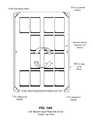
- FIG. 12Ais a perspective illustration of a SSD that includes more than one circuit board and an improved enclosure assembly which complies with the 3.5′′ HDD standard form factor in accordance with yet another embodiment of the present invention
- FIG. 12Bis an exploded view of the embodiment disclosed in FIG. 12A ;
- FIG. 12Cis a bottom perspective view of the top cover plate illustrated in FIG. 12A ;
- FIG. 12Dis a top perspective view of the disclosed in FIG. 12A ;
- FIG. 12Eis a bottom perspective view of the spacer disclosed in FIG. 12D ;
- FIG. 12Fis a bottom view of the spacer disclosed in FIG. 12E ;
- FIG. 12Gis a partial cross sectional view of section F-F of FIG. 12A of the circuit boards that include board-to-board connectors;
- FIG. 13is a cross-sectional perspective view of a 3.5 inch HDD form factor compliant enclosure assembly supporting more than two circuit boards in accordance with yet another embodiment of the present invention.
- FIGS. 14A-Cdisclose various inventive concepts relating to a 2.5 inch HDD form factor compliant SSD that has an enclosure assembly which can support more than one circuit board in accordance with yet another embodiment of the present invention
- FIG. 14Dis a bottom perspective view of a spacer for the embodiment disclosed in FIG. 14A in accordance with yet another embodiment of the present invention.
- FIG. 14Eis bottom view of the spacer in FIG. 14D ;
- FIG. 14Fis an exploded sectional view of Section G-G in FIG. 14A ;
- FIG. 14Gis a top view illustration of the bottom cover plate in FIG. 14A ;
- FIG. 14His a bottom view of the top cover plate in FIG. 14A ;
- FIG. 15is a cross-sectional perspective illustration a 2.5 inch HDD form factor compliant enclosure assembly supporting more than two circuit boards in accordance with yet another embodiment of the present invention.
- FIG. 16is a cross-sectional view of a SSD enclosure assembly having a bottom cover plate that includes a surface which is extended closer to at least one component on a circuit board is disclosed in accordance with yet another embodiment of the present invention.
- the present inventionpertains to a hard disk drive form factor compatible solid-state storage device, named “SSD”, enclosure that protects circuit boards contained within the enclosure from environmental disruption, such as mechanical stress, external electronic disruption, or any combination of these, while allowing for a variable number of circuit boards in the SSD enclosure.
- SSDhard disk drive form factor compatible solid-state storage device
- the solid-state storage device enclosure or a similar circuit board assemblyincludes an alignment guide that precludes a circuit board from being misaligned or mis-installed within the enclosure.
- One such enclosuremay have an external dimension that complies with standard hard disk drive (HDD) standard form factors, such as 3.5 inch, 2.5 inch, 1.8 inch, 1 inch, and the like, commonly employed by computer storage device manufacturers. These form factors include a number that roughly indicates the width of the storage device but may also indicate a mounting location and type, exterior dimensions of length, width and height, and interface connector type and placement. Storage devices that comply with the same HDD form factor in terms of width and length may vary considerably in height and still be considered to comply with the same form factor.
- HDDhard disk drive
- Complying with a standard HDD form factorenables manufacturers of storage devices to avoid custom-fitting and to maximize the compatibility of their HDD form factor compliant storage devices with a variety of different host computers and storage cases and racks, including desktops, notebook, rack-mounted servers and cases, blade servers, raid arrays, SANs, NAS, and other devices that use digital mass storage devices storage.
- a solid-state storage deviceis intended to refer to a mass-storage device that performs the same or substantially similar function of a HDD but does not use any moving parts or media. SSD devices and circuit boards used in such SSD devices are known by those of ordinary skill in the art, and thus, are not further disclosed herein to avoid unnecessarily complicating this disclosure.
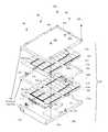
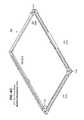
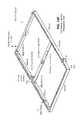
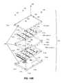
- FIGS. 1A-1Jrelate to a solid-state storage device 96 , named “SSD” that includes a single circuit board 104 and an improved enclosure assembly 98 in accordance with one embodiment of the present invention.
- This embodimentmay also be herein referred to as a SSD having a single-stack 3.5 inch form factor compliant SSD enclosure assembly.
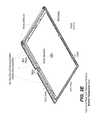
- Enclosure assembly 98includes a set of enclosure portions, such as a top cover plate 100 and a bottom cover plate 102 , which are disposed to interlock and stack with each other as well as receive circuit board 104 .
- Top cover plate 100includes a rib 105 which is located on the perimeter of top cover plate 100 . Rib 105 provides additional stiffness to top cover plate 100 .
- Bottom cover plate 102is disposed with an alignment guide 97 and a tab 99 .
- Circuit board 104is coupled between top and bottom cover plates 100 and 102 , which are fastened together by suitable fasteners, such as a set of eight flat head screws 106 .
- top and bottom cover plates 100 and 102form enclosure assembly 98 and result in a SSD having at least one circuit board, such as circuit board 104 , received within an enclosure assembly that complies with a standard HDD form factor.
- Enclosure assembly 98is disposed to receive circuit board 104 within rib 105 and to distribute mechanical stress across enclosure assembly 98 .
- Circuit board 104includes memory devices, such as NAND flash, a controller integrated circuit for controlling these memory devices, and an interface connector 130 .
- enclosure assembly 98complies with the 3.5 inch HDD form factor although the present invention is not intended to be limited to this particular form factor and other form factors may be used.
- Top and bottom cover plates 100 and 102include surfaces 107 a and 107 b , respectively.
- a perimeter edge portion 108 of circuit board 104is coupled to and located between two enclosure portions of enclosure assembly 98 .
- perimeter edge portion 108is coupled to surfaces 107 a and 107 b and is located adjacent to a rib interior surface 110 of rib 105 .
- Another alignment guide 112 and tab 114are utilized although the number of alignment guides and tabs used to interlock and stack at least two enclosure portions is not intended to be limiting in any way.
- rib 105includes notches 116 a and 116 b for receiving tabs 99 and 114 , respectively.
- notches 116 a and 116 bare formed on a surface of and into rib 105 and have a depth that does not exceed the rib width 122 of rib 105 , creating voids for receiving tabs 99 and 114 , respectively.
- the number of notches formed on rib 105is not intended to be limiting although the number of notches formed equals the number of tabs used in the embodiment shown.
- the shape of the tabs and notchesare also not intended to limit the scope and spirit of the invention disclosed.
- Alignment guide 97has a height that extends through and exceeds the thickness of perimeter edge portion 108 .
- Alignment guide 112also has a height that extends through and exceeds the thickness of another perimeter edge portion of circuit board 104 .
- the positions of alignment guides 97 and 112 on bottom cover plate 102are selected so that when a circuit board is coupled to surfaces 107 a and 107 b , the circuit board includes notches 120 a and 120 b that can receive alignment guides 97 and 112 , respectively.
- alignment guides 97 and 112may be positioned in an offset position relative to each other that prevents circuit board 104 from being coupled between surfaces 107 a and 107 b (see also FIG. 11 ) in the wrong orientation.
- Alignment guides 97 and 112 , tabs 99 and 114 , rib 105 and rib notches 116 A and 116 acollectively function as an interlocking and stacking mechanism that permits enclosure portions to be interlocked and stacked together.
- this interlocking and stacking mechanismdistributes mechanical stress, such as torsion, across the enclosure portions of enclosure assembly 98 , reducing the amount of disruptive or damaging mechanical stress that might otherwise be transmitted to circuit board 104 .
- positioning alignment guides 97 and 112 in an offset position relative to each otherprovides for a “fool-proof” assembly of SSD 96 because this prevents a circuit board with matching notches, such as circuit board 104 , from being coupled between surfaces of enclosure portions, such as surfaces 107 a and 107 b in the wrong orientation 124 .
- the positions of alignment guides 97 and 114are offset relative to each other, precluding circuit board 104 from inadvertently being placed upside down relative to one of the enclosure portions of enclosure assembly 98 , such as bottom cover plate 102 .
- Alignment guides 97 and 114are aligned on the same plane with each other but are positioned from a center axis, such as center axis 126 , at different distances, resulting in an offset position relative to each other. Center axis 126 is shown projected along the middle of length 128 of enclosure assembly 98 . Alignment guide 97 is positioned at the middle of length 128 on bottom cover plate 102 , while alignment guide 114 is offset from alignment guide 97 at a distance D 1 from middle the middle of length 128 .
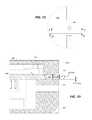
- rib 105is formed so that it has a rib extension length 118 that extends from surface 107 a .
- Rib extension length 118is selected so that the circuit board portion 108 is coupled between surfaces 107 a and 107 b during assembly. For instance, if rib extension length 118 is disposed to have a length that is less than the mean thickness of circuit board portion 108 , surfaces 107 a and 107 b will contact and hold circuit board portion 108 . Besides contacting and holding circuit board portion 108 , surfaces 107 a and 107 b dampen vibration forces imparted on circuit board 104 .
- rib extension length 118is selected to have a length that is equal to the distance between surfaces 107 a and 107 b when circuit board portion 108 is coupled between these surfaces subtracted by the absolute value of the negative tolerance used to manufacture circuit board portion 108 .
- rib extension length 118may be disposed to have a length of 2 mm minus 0.13 mm, which is equal to 1.87 mm. Using a rib extension length 118 that is less than the distance between surfaces 107 a and 107 b creates a gap 117 a.
- Rib extension length 118also protects circuit board 104 from electronic disturbance due to electro-static discharge (ESD), electro-magnetic interference (EMI), or both.
- Rib 105may be also coupled to an electrical ground (not shown) used by circuit board 104 to further increase this electronic disturbance protection. Further still, rib 105 further stiffens top cover plate 100 , which further minimizes mechanical disturbance due to vibration which may be transferred circuit board 104 .
- top cover plate 100 and bottom cover plate 102are provided with top center post 132 and bottom center post 134 , respectively, while circuit board 104 includes a board aperture 136 .
- Top and bottom center posts 132 and 134are located approximately within the respective centers of top and bottom cover plates 100 and 102 .
- the location of board aperture 136is selected so that when circuit board 104 is coupled between top and bottom cover plates 100 and 102 during assembly as previously described, top and bottom center posts 132 and 134 and board aperture 136 are in-line with each other so that a fastener of sufficient length, such as 106 , couples top cover plate 100 with bottom cover plate 102 and passes through board aperture 136 as illustrated in FIG. 1J .
- Providing top and bottom center posts 132 and 134further stabilizes circuit board 104 from mechanical disturbance, such as vibration, although this functional advantage provided by these center posts is not intended to limit the scope of the present invention.
- the portions comprising enclosure assembly 98may be formed by using a variety of manufacturing processes, and may be milled, die-casted, stamped, injection-molded (plastic), and the like.
- the design of enclosure assembly 98permits the interchange of parts that have been formed using different manufacturing processes.
- a SSD 140that includes an improved enclosure assembly 142 having enclosure portions that have been formed using different manufacturing processes.
- One enclosure portionis formed by stamping, such as stamped top cover plate 144
- the other enclosure portionis formed by die-casting, such as bottom cover plate 102 .
- SSD 140is substantially similar to SSD 98 except SSD 98 is shown using an enclosure assembly that employs a stamped top cover plate 144 , and fasteners sized to compensate for the different any difference in thickness between stamped cover plate 144 and top cover plate 100 .
- screws 146are used to fasten stamped cover plate 144 to bottom cover plate 102 and have screw lengths that are suitable for coupling to bottom cover plate 102 when SSD 140 is fully assembled.
- Stamped cover plate 144includes notches that receive and interlock with the tabs of bottom cover plate 102 , such as tabs 99 and 114 illustrated also in FIG. 1B and FIGS. 1E-I . Additional views of stamped cover plate 144 are provided in FIGS. 2B-2E
- FIG. 3is a perspective view of the mounting positions to which fasteners may be applied to couple a 3.5 inch HDD form factor compliant SSD, such as SSD 96 or 140 above, to a computer or storage appliance case in accordance with yet another embodiment of the present invention.
- SSD 96 or 140includes mounting positions that comply with the HDD form factor selected for enclosure assembly 98 .
- enclosure assembly 98includes mounting positions 150 a - 150 d that are located on the bottom surface of bottom cover plate 102 and mounting positions 152 a - 152 c on the sides of bottom cover plate 102 .
- Bottom cover plate 102also includes additional mounting positions disposed on the other side of bottom cover plate 102 but are not illustrated in this figure due to its perspective view.
- FIG. 4Ais a perspective view of a 3.5 inch HDD form factor compliant SSD 156 that has an improved enclosure assembly substantially similar to enclosure assembly 98 above, but is configured with a fibre channel interface connector 158 in accordance with yet another embodiment of the present invention.
- FIG. 4Bis a perspective view of a 3.5 inch HDD form factor compliant SSD 160 that has an improved enclosure assembly substantially similar to enclosure assembly 98 above, but is configured with a SCSI U320 channel interface connector 162 in accordance with yet another embodiment of the present invention.
- FIG. 4Cis a perspective view of a 3.5 inch HDD form factor compliant SSD 164 that has an improved enclosure assembly substantially similar to enclosure assembly 98 above, but is configured with a SATA channel interface connector 166 in accordance with yet another embodiment of the present invention.
- the present inventionis not limited to a particular type of interface connector, including those shown herein, but may be any interface connector that is compatible with the interface protocol used by the SSD manufactured.
- the SSDs disclosed hereinmay have other types of interface connectors, such as PATA, iSCSI, and the like.
- FIG. 5is a partial perspective view of a 3.5 inch HDD form factor compliant SSD, such as SSD 96 or 140 above, that includes a jumper header 168 , an LED display 170 and a system connector 172 in accordance with yet another embodiment of the present invention.
- Jumper header 168may be used to set and monitor signals sent to LED display 170
- system connector 172may be used to provide firmware upgrades to the SSD.
- FIGS. 6A-6Billustrate a SSD 196 that includes a single circuit board 204 and an improved enclosure assembly 198 that complies with the 2.5′′ HDD standard form factor in accordance with another embodiment of the present invention.
- This embodimentmay also be herein referred to as a SSD having a single-stack 2.5 inch form factor compliant SSD enclosure assembly.
- Enclosure assembly 198includes a set of enclosure portions, such as a top cover plate 200 and a bottom cover plate 202 , which are disposed to interlock and stack with each other as well as receive circuit board 204 .
- Top cover plate 200includes a rib 205 which is located on the perimeter of top cover plate 200 . Rib 205 provides additional stiffness to top cover plate 200 .
- Bottom cover plate 202is disposed with an alignment guide 197 , but unlike bottom cover plate 102 above, bottom cover plate is configured without a tab in this particular example.
- Circuit board 204is coupled between top and bottom cover plates 200 and 202 , which are fastened together by suitable fasteners, such as a set of six flat head screws 206 .
- top and bottom cover plates 200 and 202form enclosure assembly 198 and result in a SSD having at least one circuit board, such as circuit board 204 , that is received within an enclosure assembly that complies with a standard HDD form factor.
- Enclosure assembly 198is disposed to receive circuit board 204 within rib 205 and to distribute mechanical stress across enclosure assembly 198 .
- Enclosure assembly 198complies with the 2.5 inch HDD form factor although the present invention is not intended to be limited to this particular form factor and other form factors may be used.
- top and bottom cover plates 200 and 202include surfaces 207 a and 207 b , respectively.
- a perimeter edge portion 208 of circuit board 204is coupled to and located between two enclosure portions of enclosure assembly 198 .
- perimeter edge portion 208is coupled to surfaces 207 a and 207 b and is located adjacent to an interior rib surface 210 of rib 205 .
- FIGS. 6B , 6 D, 6 G and 6 Htop and bottom cover plates 200 and 202 include surfaces 207 a and 207 b , respectively.
- rib 205includes notches, such as 216 a - 216 c , for receiving the alignment guides included on bottom cover plate 202 .
- Notches 216 a - care formed on a surface of and into rib 205 so that they form voids for receiving their respective alignment guides, such as alignment guides 197 and 212 a - c , respectively.
- the number of notches formed on rib 205is not intended to be limiting although the number of notches formed equals the number of tabs used in the embodiment shown. Moreover, the shape of the tabs and notches are also not intended to limit the scope and spirit of the invention disclosed.
- Alignment guides 197 and 212 a - ceach have a height that extends through and exceeds the thickness of perimeter edge portion 209 . As shown in FIGS. 6B , 6 E- 6 F and 6 I, the positions of alignment guides 197 and 212 a - c on bottom cover plate 202 are selected so that a circuit board disposed with circuit board notches 217 a - 217 d can be received within alignment guides 197 and 212 a - c , enabling the circuit board to is also contact surface 207 b of bottom cover plate 202 .
- Alignment guides 197 and 212 a - c , notches 21 a - c of top cover plate 200 , and rib 205form an interlocking and stacking mechanism that permits enclosure portions to be stacked together.
- this interlocking and stacking mechanismdistributes mechanical stress, such as torsion, across the enclosure portions of enclosure assembly 198 , reducing the amount of disruptive or damaging mechanical stress that might otherwise be transmitted to circuit board 204 .
- alignment guide 197has a shape, dimension, or both that is different than the shape, dimension, or both of at least one of the alignment guides, such as 216 a - 216 c to prevent circuit board 204 from being coupled between surfaces 207 a and 207 b in the wrong orientation. This also prevents a circuit board with matching circuit board notches, such as circuit board 204 , from being coupled between surfaces of enclosure portions, such as surfaces 207 a and 207 b in the wrong orientation 224 , resulting in a “fool-proof” assembly of SSD 196 .
- rib 205is formed so that it has a rib extension length 218 that extends from surface 207 a .
- Rib extension length 218is selected so that circuit board portion 208 is coupled between surfaces 207 a and 207 b during assembly. For instance, if rib extension length 218 is disposed to be less than the mean thickness of circuit board portion 108 , surfaces 207 a and 207 b will contact and hold circuit board portion 208 . Besides contacting and holding circuit board portion 208 , surfaces 207 a and 207 b dampen vibration forces imparted on circuit board 204 .
- rib extension length 218is selected to have a length that is equal to the distance between surfaces 207 a and 207 b when circuit board portion 208 is coupled between these surfaces subtracted by the absolute value of the negative tolerance used to manufacture circuit board portion 208 .
- rib extension length 218may be disposed to have a length of 2 mm minus 0.13 mm, which is equal to 1.87 mm. Using a rib extension length 218 that is less than the distance between surfaces 207 a and 207 b creates a gap 117 b.
- Rib extension length 218also protects circuit board 204 from electronic disturbance due to electro-static discharge (ESD), electro-magnetic interference (EMI), or both.
- Rib 205may be also coupled to an electrical ground (not shown) used by circuit board 204 to further increase this electronic disturbance protection. Further still, rib 205 further stiffens top cover plate 200 , which further minimizes mechanical disturbance due to vibration which may be transferred circuit board 204 .
- the portions comprising enclosure assembly 198may be formed by using a variety of manufacturing processes, and may be milled, die-casted, stamped, injection-molded (plastic), and the like.
- the design of enclosure assembly 198permits the interchange of parts that have been formed using different manufacturing processes.
- a SSD 230includes an improved enclosure assembly 232 having stamped enclosure portions. Both top cover plate 234 and bottom cover plate 235 are manufactured using a manufacturing process that includes stamping.
- Bottom cover plate 235includes a flanges 237 a - b disposed on at least two sides of its perimeter so that at two respective side edges of top cover plate 234 are received within the inside facing surfaces of flanges 237 a and 237 b .
- SSD 230is substantially similar to SSD 196 except SSD 230 is shown using an enclosure assembly that employs a stamped top and bottom cover plates 234 and 235 , and fasteners that are have sized to compensate for the different any difference in thickness between stamped cover plate 234 and top cover plate 200 .
- screws 236are used to fasten stamped top cover plate 234 to bottom cover plate 235 , and screws 236 have screw lengths that are suitable for coupling to top cover plate 234 to bottom cover plate 235 .
- FIG. 8illustrates a SSD 240 that includes an improved enclosure assembly 232 having enclosure portions that have been formed using different manufacturing processes.
- One enclosure portionis formed by stamping, such as stamped bottom cover plate 244 ; while the other enclosure portion is formed by die-casting, such as top cover plate 200 .
- SSD 240is substantially similar to SSD 196 except SSD 240 is shown using an enclosure assembly that employs a stamped bottom cover plate 244 and fasteners that are have sized to compensate for the different any difference in thickness between stamped bottom cover plate 244 and top cover plate 200 .
- screws 246are used to fasten top cover plate 200 to stamped bottom cover plate 244 .
- Screws 246have screw lengths that are suitable for coupling top cover plate 200 to bottom cover plate 244 .
- Top cover plate 248is substantially similar to top cover plate 200 disclosed with respect to FIGS. 6A-6D
- bottom cover plate 244is substantially similar to bottom cover plate 235 disclosed with respect to FIG. 7 .
- FIG. 9is a perspective view of the mounting positions to which fasteners may be applied to couple a 2.5 inch HDD form factor compliant SSD, such as SSD 196 above, with a computer or storage appliance case in accordance with yet another embodiment of the present invention.
- SSD 196includes mounting positions that comply with the HDD form factor selected for enclosure assembly 198 .
- enclosure assembly 198includes mounting positions 250 a - 250 h that are located on the bottom surface of bottom cover plate 202 and mounting positions 252 a - 252 d on the sides of bottom cover plate 202 .
- Bottom cover plate 202also includes additional mounting positions disposed on the other side of bottom cover plate 202 but are not illustrated in this figure due to its perspective view.
- FIG. 10Ais a perspective view of a 2.5 inch HDD form factor compliant SSD 256 that has an improved enclosure assembly substantially similar to enclosure assembly 198 above, but is configured with a SATA interface connector 258 in accordance with yet another embodiment of the present invention.
- FIG. 10Bis a perspective view of a 2.5 inch HDD form factor compliant SSD 260 that has an improved enclosure assembly substantially similar to enclosure assembly 198 above, but is configured with a PATA interface connector 262 in accordance with yet another embodiment of the present invention.
- FIG. 11is a partial perspective view of a 2.5 inch HDD form factor compliant SSD, such as SSD 196 or 230 above, that has an enclosure assembly 261 having openings for providing access to a jumper header 264 , an LED display 266 and a system connector 268 in accordance with yet another embodiment of the present invention.
- Jumper header 264may be used to set and monitor signals sent to LED display 266
- system connector 268may be used to provide firmware upgrades to the SSD.
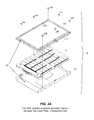
- FIGS. 12A-12Fdisclose various inventive concepts relating to a 3.5 inch HDD form factor compliant SSD 280 that has an enclosure assembly 286 that can support more than one circuit board, such as circuit boards 282 and 284 .
- Enclosure assembly 286is similar to enclosure assembly 98 or 142 supporting a single circuit board SSD, such as SSD 96 or 140 , which complies with the 3.5 inch HDD form factor disclosed previously above.
- Enclosure assembly 286includes enclosure portions comprising top cover plate 300 and bottom cover plate 302 .
- Top and bottom cover plates 300 and 302are substantially similar to those disclosed with respect to enclosure assemblies 98 and 142 , such as top cover plate 100 or 144 and bottom cover plate 102 .
- top cover plate 300includes a rib 304 having an interior surface 310 , notches 316 a and 316 b , a top center post 332 , and a surface 307 a which are substantially similar to rib 105 , interior surface 110 , notches 116 a and 116 b , top center post 132 and surface 107 a , respectively, of top cover plate 100 previously disclosed above.
- Bottom cover plate 302includes alignment guides 311 and 312 , tabs and a bottom center post 334 , and a surface 307 b , which are respectively and substantially similar to alignment guides 97 and 112 , tabs 99 and 114 , bottom center post 134 , and surface 107 b previously disclosed above. Unlike enclosure assembly 98 or 142 , however, enclosure assembly 286 further comprises a spacer 288 .
- Spacer 288 , top cover plate 300 and a bottom cover plate 302are disposed to interlock and stack with each other as well as receive circuit boards 282 and 284 .
- spacer 288includes a cross-member 270 , spacer center post 272 , alignment guides 274 and 276 , tabs 278 and 294 , a rib 290 , an interior rib surface 292 , and surfaces 309 a and 309 b .
- the number of alignment guides and tabs provided or disposed on spacer 288is not intended to be limiting, although in the embodiment shown, the number of alignment guides and tabs used on spacer 288 is respectively equal to the number of alignment guides and tabs selected for top and bottom cover plates 300 and 302 .
- Rib 290is located on the perimeter of spacer 288 and provides additional stiffness to spacer 288 .
- Circuit board 282is coupled between bottom cover plate 302 and one side of spacer 290
- circuit board 284is coupled between top cover plate 300 and another side of spacer 288 .
- Circuit boards 282 and 284 , spacer 288 , top cover plate 300 and bottom cover plate 302are fastened together by suitable fasteners, such as a set of eight flat head screws 306 .
- suitable fastenerssuch as a set of eight flat head screws 306 .
- circuit board 282includes memory devices, such as NAND flash, a controller integrated circuit for controlling these memory devices, and an interface connector 296 , and a board-to-board connector 295 .
- circuit board 284may be used as a memory expansion board and may include additional memory components and a board-to-board connector 293 that can electrically couple to board-to-board connector 295 .
- perimeter edge portion 308 of circuit board 282 and perimeter edge portion 305 of circuit board 284are each coupled to and located between two enclosure portions of enclosure assembly 286 .
- perimeter edge portion 308is coupled to and located between bottom cover plate 302 at surface 307 b and spacer 288 at surface 309 b
- perimeter edge portion 305is coupled to and located between top cover plate 300 at surface 307 a and spacer 288 at surface 309 a .
- Perimeter edge portion 308is adjacent to interior rib surface 292 of rib 290 when circuit board 305 is placed between bottom cover plate 302 and spacer 288 .
- Perimeter edge portion 305is adjacent to interior rib surface 310 of rib 304 when circuit board 284 is placed between top cover plate 300 and spacer 288 .
- Rib 290includes notches 318 a and 318 b for receiving tabs 298 and 314 , respectively, and rib 304 includes notches 316 a and 316 b for receiving tabs 278 and 294 .
- Rib 290includes notches 318 a and 318 b for receiving tabs 298 and 314 , respectively, and rib 304 includes notches 316 a and 316 b for receiving tabs 278 and 294 .
- notches 316 a - 316 b and 318 a - 318 bare each respectively formed on a surface of and into ribs 290 and 304 , and have a depth that does not exceed rib widths 322 and 324 , creating voids for receiving tabs 274 and 294 and tabs 298 and 314 , respectively.
- the number of notches formed on ribs 290 and 304is not intended to be limiting.
- the shape of the tabs and notchesare also not intended to limit the scope and spirit of the invention disclosed.
- Alignment guides 274 and 276 and alignment guides 311 and 312each have a height that extends through and exceeds the thickness of perimeter edge portions 284 and 308 , respectively. As shown in FIGS. 12B-12D , the positions of alignment guides 274 and 276 that are disposed on spacer 288 , and alignment guides 311 and 312 that are disposed on bottom cover plate 302 , are selected so circuit board notches 320 a - 320 b and circuit board notches 326 a - 326 b respectively receive these alignment guides during assembly.
- Alignment guides 274 , 276 , 311 , and 312 ; tabs 294 , 278 , 298 , 314 , ribs 290 and 304 , and notches 316 a - 316 b and 318 a - 318 bcollectively function as an interlocking and stacking mechanism that permits enclosure portions, such as spacer 288 , top cover plate 300 and bottom cover plate 302 , to be interlocked and stacked together.
- this interlocking and stacking mechanismdistributes mechanical stress, such as torsion, across the enclosure portions of enclosure assembly 286 , reducing the amount of disruptive or damaging mechanical stress that might otherwise be transmitted to circuit boards 282 and 284 .
- these alignment guides from the same enclosure portionmay be positioned in an offset position relative to each other that prevents a circuit board from being coupled between enclosure portions in the wrong orientation and providing a “fool-proof” assembly of SSD 280 because this prevents a circuit board with matching notches, such as circuit board 282 or 284 , from being coupled in the wrong orientation between surfaces of enclosure portions, such as surfaces 307 a and 309 a , or surfaces 307 b and 309 b , respectively.
- rib 290 of spacer 288 in FIG. 12E and rib 304 of top cover plate 300 in FIG. 12Care each formed so that they have rib extension length 330 and rib extension length 336 , respectively.
- Rib extension lengths 330 and 336respectively extend from surfaces 309 a and 307 a , respectively, in substantially the same manner as described for rib extension length 118 or 218 disclosed above.
- rib extension lengths 330 and 336create gaps 117 c , as shown in FIG. 13 below.
- Rib extension lengths 330 and 336also protect circuit boards 282 and 284 from electronic disturbance due to electro-static discharge (ESD), electro-magnetic interference (EMI), or both.
- Ribs 290 and 304may be also coupled to an electrical ground (not shown) used by these circuit boards to further increase this electronic disturbance protection.
- Ribs 290 and 304further stiffen spacer and top cover plate 300 , respectively, which further minimizes mechanical disturbance due to vibration which may be transferred circuit boards 282 and 284 .
- Enclosure assembly 338includes enclosure portions comprising top cover plate 340 and bottom cover plate 342 , which are substantially similar to those disclosed with respect to enclosure assemblies 98 , 142 , or 286 , such as top cover plate 100 , 144 or 300 , and bottom cover plate 102 or 302 , disclosed previously.
- top cover plate 340includes a rib 344 having an interior rib surface, at least two notches, a top center post and a surface which are respectively and substantially similar to rib 304 , interior surface 310 , notches 316 a and 316 b , top center post 332 and surface 307 a of top cover plate 300 .
- Bottom cover plate 302includes alignment guides, tabs, a bottom center post, and a surface, which are respectively and substantially similar to alignment guides 311 and 312 , tabs 298 and 314 , bottom center post 334 , and surface 307 b previously disclosed above.
- enclosure assembly 338comprises more than one spacer, such as spacer 350 .
- Spacer 350is substantially similar to spacer 288 previously disclosed above with respect to FIGS. 12A-12C .
- Top cover plate 340 , bottom cover plate 242 , and multiple instances of spacer 350are disposed to interlock and stack with each other as well as receive circuit boards 346 and 348 . These circuit boards are coupled to each other through board-to-board connectors and are received by enclosure assembly 338 .
- This board-to-board connectoris not illustrated in FIG. 13 but is substantially similar to board-to-board connectors 293 and 295 , previously disclosed with respect to FIG. 12F .
- Circuit boards 346 and 348are substantially similar to circuit board 284 and 282 , respectively disclosed above with respect to FIGS. 12A and 12B .
- spacer 350Using multiple instances of spacer 350 enables a SSD that includes enclosure assembly 238 to receive more than one circuit board disposed with memory devices, such as circuit board 346 , enabling this SSD to remain suitable for mounting in systems that require 3.5′′ HDD form factor compliant storage devices and that can receive such storage devices but with different enclosure assembly heights.
- FIGS. 14A-14Gdisclose various inventive concepts relating to a 2.5 inch HDD form factor compliant SSD 358 that has an enclosure assembly 360 which can support more than one circuit board, such as circuit boards 362 and 364 .
- Enclosure assembly 360is similar to an enclosure assembly that supports a single circuit board SSD which complies with the 2.5 inch HDD form factor disclosed previously above. Examples of such an enclosure assembly and SSD include enclosure assembly 198 , 232 , or 242 and SSD 196 , 230 or 240 , which were previously disclosed with respect to FIGS. 6A-6I , FIG. 7 , or FIG. 8 , respectively.
- Enclosure assembly 360includes enclosure portions comprising top cover plate 366 and bottom cover plate 368 .
- Top and bottom cover plates 366 and 368are substantially similar to those disclosed with respect to enclosure assemblies 198 , 232 , and 242 , such as top cover plate 200 or 234 , and such as bottom cover plate 202 or 244 .
- top cover plate 366includes a rib 370 having an interior rib surface 372 , notches 374 a - c , and a surface 376 a which are respectively and substantially similar to rib 205 , interior rib surface 210 , notches 216 a - c , and surface 207 a of top cover plate 200 previously disclosed above.
- Bottom cover plate 368includes a surface 376 b and alignment guides 378 a - c , which are respectively and substantially similar to surface 207 b and alignment guides 197 and 212 a - c , previously disclosed above for bottom cover plate 202 in FIGS. 6A and 6B .
- enclosure assembly 360further comprises a spacer 380 .
- spacer 380includes alignment guides 382 a - c , a rib 384 , an interior rib surface 386 , and surfaces 388 a - b , which are substantially similar to alignment guides 197 and 212 a - c , a rib 290 , an interior rib surface 210 , and surfaces 207 a and 207 b in FIGS. 6A-6D .
- Spacer 380also includes notches disposed on the corners of spacer 380 , such as notches 389 a - c .
- the number of alignment guides and notches disposed on spacer 380is not intended to be limiting although in the current embodiment the number of alignment guides and notches used on spacer 380 is respectively equal to the number of notches and alignment guides selected for top and bottom cover plates 366 and 368 , respectively.
- Spacer 380 , top cover plate 366 and a bottom cover plate 368are disposed to interlock and stack with each other as well as receive circuit boards 362 and 364 .
- Rib 384is located on the perimeter of spacer 380 and provides additional stiffness to spacer 380 .
- Circuit board 364is coupled between bottom cover plate 368 and one side of spacer 380 , such as surface 388 b .
- Circuit board 362is coupled between top cover plate 366 and another side of spacer 380 , such as surface 388 a .
- Circuit boards 362 and 366 , spacer 380 , top cover plate 366 and bottom cover plate 368are fastened together by suitable fasteners, such as a set of six flat head screws 390 .
- circuit board 364includes memory devices, such as NAND flash, a controller integrated circuit for controlling these memory devices, and an interface connector 392 , and a board-to-board connector 394 .
- Circuit board 362may be used as a memory expansion board and may include additional memory components and a board-to-board connector 396 that can electrically couple to board-to-board connector 394 .
- perimeter edge portion 398 of circuit board 362 and perimeter edge portion 400 of circuit board 364are each coupled to and located between two enclosure portions of enclosure assembly 360 .
- perimeter edge portion 400is coupled to and located between bottom cover plate 368 at surface 376 b and spacer 380 at surface 388 b .
- Perimeter edge portion 400is adjacent to interior rib surface 386 of rib 384 when circuit board 364 is placed between bottom cover plate 368 and spacer 380 .
- perimeter edge portion 398is coupled to and located between top cover plate 366 at surface 376 a and spacer 380 at surface 388 a .
- Perimeter edge portion 398is adjacent to interior rib surface 404 of rib 370 when circuit board 362 is placed between top cover plate 366 and spacer 380 .
- the stacking of spacer 380 , top cover plate 366 and bottom cover plate 368involves using notches 374 a - d and 389 a - d and alignment guides 378 a - d and 382 a - d .
- Notches 374 a - dreceive alignment guides 382 a - d , respectively, and notches 389 a - d receive alignment guides 378 a - d .
- notches 374 a - c and notches 389 a - care each respectively formed on a surface of and into ribs 370 and 384 .
- notches 374 a - c of top cover plate 366 , and notches 389 a - c of spacer 380each have a depth that does not exceed rib widths 406 and 408 , creating voids for receiving alignment guides 382 a - d and 378 a - d , respectively.
- the number of notches formed on ribs 370 and 384is not intended to be limiting.
- the shapes of the alignment guides and notches disclosed hereinare also not intended to limit the scope and spirit of the invention disclosed.
- alignment guides 378 a - d and alignment guides 382 a - deach have a height that extends through and exceeds the thickness of the portion of circuit boards 364 and 362 which are adjacent to these alignment guides, respectively.
- the positions of alignment guides 378 a - d and alignment guides 382 a - dare selected so circuit board notches 217 a - d permit circuit boards 364 and 362 to be received by bottom cover plate 368 and spacer 380 within the inside surfaces of their respective alignment guides during assembly.
- circuit boards 362 and 364have the same length and width dimensions.
- alignment guides 378 a - d of bottom cover plate 368 , alignment guides 382 a - d of spacer 380 , ribs 384 and 370 , and notches 389 a - c and 374 a - ccollectively function as an interlocking and stacking mechanism that permits enclosure portions, such as spacer 380 , top cover plate 366 and bottom cover plate 368 to be interlocked and stacked together.
- this interlocking and stacking mechanismdistributes mechanical stress, such as torsion, across the enclosure portions of enclosure assembly 360 , reducing the amount of disruptive or damaging mechanical stress that might otherwise be transmitted to circuit boards 362 and 364 .
- At least one alignment guidesuch as alignment guide 382 d and 378 d , from each set of alignment guides from spacer 380 and bottom cover plate 368 , respectively, have a uniquely shaped surface that prevents a circuit board from being coupled between enclosure portions in the wrong orientation.
- Thisprovides a “fool-proof” assembly of SSD 358 by preventing a circuit board with matching notches, such as circuit board 364 and 362 , from being placed in the wrong orientation between surfaces of enclosure portions, such as surfaces 376 a and 388 b , or surfaces 388 a and 376 b , respectively.
- rib 384 of spacer 380 in FIG. 14E , and rib 370 of top cover plate 366 in FIG. 14Gare each formed so that they have rib extension lengths 414 and 416 , respectively.
- Rib extension lengths 414 and 416respectively extend from surfaces 376 a and 388 b in substantially the same manner as described for rib extension length 118 or 218 disclosed above.
- rib extension lengths 414 and 416create gaps 117 d , as shown in FIG. 15 below.
- Rib extension lengths 414 and 416also protect circuit boards 364 and 362 from electronic disturbance due to electro-static discharge (ESD), electro-magnetic interference (EMI), or both.
- Ribs 384 and 370may be also coupled to an electrical ground (not shown) used by these circuit boards to further increase this electronic disturbance protection.
- ribs 384 and 370further stiffen spacer 380 and top cover plate 366 , respectively, which further minimizes mechanical disturbance due to vibration which may be transferred circuit boards 364 and 362 .
- FIG. 15another embodiment of a 2.5 inch HDD form factor compliant enclosure assembly 418 supporting more than two circuit boards is shown.
- This embodimentmay also be herein referred to as a multi-stack 2.5 inch form factor compliant SSD enclosure assembly.
- Enclosure assembly 418is similar to enclosure assembly 360 because it includes enclosure portions comprising top cover plate 422 and bottom cover plate 424 , which are substantially similar to those disclosed with respect to enclosure assemblies 198 or 360 , such as top cover plate 200 or 366 , and bottom cover plate 202 or 368 , which were previously disclosed above with respect to FIGS. 6A-6D and FIGS. 14A-14C , respectively.
- top cover plate 422includes a rib 426 having an interior rib surface, notches, and a surface which are respectively and substantially similar to rib 370 , interior rib surface (not yet assigned), notches 374 a - d , and surface 376 a of top cover plate 366 .
- Bottom cover plate 424includes alignment guides and a surface, which are respectively and substantially similar to alignment guides 378 a - d and surface 376 b .
- enclosure assembly 418comprises more than one spacer, such as spacer 428 .
- Spacer 428is substantially similar to spacer 380 .
- Top cover plate 422 , bottom cover plate 424 , and spacers 428are disposed to interlock and stack with each other as well as receive circuit boards 430 and 432 . These circuit boards are coupled to each other through a board-to-board connector (not shown) and are received by enclosure assembly 418 as disclosed in FIG. 15 . Increasing memory capacity may be performed by interlocking and stacking an additional circuit board and spacer, while decreasing memory capacity may be performed by removing a circuit board and spacer from enclosure assembly 418 . When using screws to fasten enclosure assembly 418 would obviously require screws of different lengths based on the number of spacers and circuit boards used. Circuit boards 430 and 432 are substantially similar to circuit board 364 and 362 , respectively, in FIGS. 14A-14C .
- spacer 428permits a SSD that includes enclosure assembly 418 to receive more than one circuit board disposed with memory devices, such as circuit board 432 , enabling this SSD to remain suitable for mounting in systems that require a 2.5′′ HDD form factor compliant storage device and that can receive storage devices of different heights.
- an enclosure assembly 438 having a bottom cover plate 442 that includes a surface 444 which is extended closer to at least one component 446 on a circuit board 448is disclosed in accordance with yet another embodiment of the present invention.
- Component 446dissipates heat during operation of component 446 .
- Enclosure assembly 438may be used as part of a HDD form factor compliant SSD, such as those previously disclosed above, and further includes top cover plate 440 .
- a thermal pad 450is placed between surface 444 and component 446 so that thermal pad 450 contacts surface 444 and component 446 .
- top and bottom cover plates 440 and 442are substantially similar in form and function as other top and bottom cover plates disclosed above, except bottom cover plate 442 has been modified to include surface 444 .
Landscapes
- Engineering & Computer Science (AREA)
- Microelectronics & Electronic Packaging (AREA)
- Casings For Electric Apparatus (AREA)
Abstract
Description
Claims (21)
Priority Applications (3)
| Application Number | Priority Date | Filing Date | Title |
|---|---|---|---|
| US12/876,094US8665601B1 (en) | 2009-09-04 | 2010-09-03 | Solid state drive with improved enclosure assembly |
| US14/182,303US9552848B2 (en) | 2009-09-04 | 2014-02-18 | Solid state drive with improved enclosure assembly |
| US15/414,504US10149399B1 (en) | 2009-09-04 | 2017-01-24 | Solid state drive with improved enclosure assembly |
Applications Claiming Priority (2)
| Application Number | Priority Date | Filing Date | Title |
|---|---|---|---|
| US23978709P | 2009-09-04 | 2009-09-04 | |
| US12/876,094US8665601B1 (en) | 2009-09-04 | 2010-09-03 | Solid state drive with improved enclosure assembly |
Related Child Applications (1)
| Application Number | Title | Priority Date | Filing Date |
|---|---|---|---|
| US14/182,303ContinuationUS9552848B2 (en) | 2009-09-04 | 2014-02-18 | Solid state drive with improved enclosure assembly |
Publications (1)
| Publication Number | Publication Date |
|---|---|
| US8665601B1true US8665601B1 (en) | 2014-03-04 |
Family
ID=50158792
Family Applications (3)
| Application Number | Title | Priority Date | Filing Date |
|---|---|---|---|
| US12/876,094Active2032-01-16US8665601B1 (en) | 2009-09-04 | 2010-09-03 | Solid state drive with improved enclosure assembly |
| US14/182,303Active2031-05-20US9552848B2 (en) | 2009-09-04 | 2014-02-18 | Solid state drive with improved enclosure assembly |
| US15/414,504ActiveUS10149399B1 (en) | 2009-09-04 | 2017-01-24 | Solid state drive with improved enclosure assembly |
Family Applications After (2)
| Application Number | Title | Priority Date | Filing Date |
|---|---|---|---|
| US14/182,303Active2031-05-20US9552848B2 (en) | 2009-09-04 | 2014-02-18 | Solid state drive with improved enclosure assembly |
| US15/414,504ActiveUS10149399B1 (en) | 2009-09-04 | 2017-01-24 | Solid state drive with improved enclosure assembly |
Country Status (1)
| Country | Link |
|---|---|
| US (3) | US8665601B1 (en) |
Cited By (24)
| Publication number | Priority date | Publication date | Assignee | Title |
|---|---|---|---|---|
| US20140160698A1 (en)* | 2012-12-12 | 2014-06-12 | James Farquhar | Solid-state drive housing, a solid-state disk using the same and an assembling process thereof |
| GB2523839A (en)* | 2014-03-07 | 2015-09-09 | Xyratex Tech Ltd | A solid state storage carrier and a storage system |
| US20160254612A1 (en)* | 2013-08-05 | 2016-09-01 | Continental Automotive Gmbh | Module housing for electronic assembly |
| USD768134S1 (en)* | 2010-10-18 | 2016-10-04 | Apple Inc. | Electronic device |
| US9552848B2 (en) | 2009-09-04 | 2017-01-24 | Bitmicro Networks, Inc. | Solid state drive with improved enclosure assembly |
| GB2540864A (en)* | 2015-06-12 | 2017-02-01 | Deere & Co | Electronic assembly having alignable stacked circuit boards |
| US20170188477A1 (en)* | 2015-12-28 | 2017-06-29 | Kabushiki Kaisha Toshiba | Storage device |
| US20170188473A1 (en)* | 2015-12-28 | 2017-06-29 | Kabushiki Kaisha Toshiba | Storage device |
| US10019041B2 (en) | 2016-04-20 | 2018-07-10 | Samsung Electronics Co., Ltd. | Solid state drive (SSD) housing and SSD housing assembly |
| US20180270991A1 (en)* | 2017-03-16 | 2018-09-20 | Toshiba Memory Corporation | Electronic device |
| US20180276171A1 (en)* | 2017-03-23 | 2018-09-27 | Hewlett Packard Enterprise Development Lp | Non-volatile memory drives |
| EP3515156A1 (en)* | 2018-01-19 | 2019-07-24 | Ge Aviation Systems Llc, Inc. | Control boxes and system-on-module circuit boards for unmanned vehicles |
| US20190341081A1 (en)* | 2015-12-30 | 2019-11-07 | Shenzhen Longsys Electronics Co., Ltd. | Ssd storage module, ssd component, and ssd |
| US10499507B2 (en) | 2017-12-08 | 2019-12-03 | Samsung Electronics Co., Ltd. | Solid state drive apparatus |
| US10582632B2 (en)* | 2016-06-02 | 2020-03-03 | Autonetworks Technologies, Ltd. | Board unit |
| US20200077547A1 (en)* | 2018-08-30 | 2020-03-05 | Samsung Electronics Co., Ltd. | Solid state drive apparatus including electrostatic prevention structure |
| US10595438B1 (en)* | 2019-03-22 | 2020-03-17 | Agylstor, Inc. | Rugged digital mass storage device |
| US10955882B2 (en) | 2018-03-09 | 2021-03-23 | Samsung Electronics Co., Ltd. | Solid-state drive case and solid-state drive device using the same |
| US11116088B2 (en)* | 2019-03-19 | 2021-09-07 | Toshiba Memory Corporation | Semiconductor storage device |
| US20210294386A1 (en)* | 2020-03-19 | 2021-09-23 | Nexark, Inc. | Enclosing a portable solid state device |
| DE102021110115A1 (en) | 2021-04-21 | 2022-10-27 | Lear Corporation | Container with a mechanical tolerance compensation element |
| US20220394862A1 (en)* | 2021-06-02 | 2022-12-08 | Kioxia Corporation | Semiconductor storage device |
| US20230051635A1 (en)* | 2021-08-13 | 2023-02-16 | Pegatron Corporation | Electronic device capable of discharging static electricity |
| US20230132119A1 (en)* | 2019-11-11 | 2023-04-27 | Shenzhen Unionmemory Information System Limited | Method and apparatus for upgrading ssd firmware compatible with raid ssd and non-raid |
Families Citing this family (11)
| Publication number | Priority date | Publication date | Assignee | Title |
|---|---|---|---|---|
| US10223316B2 (en)* | 2014-06-18 | 2019-03-05 | Ngd Systems, Inc. | Interface compatible with M.2 connector socket for ultra high capacity solid state drive |
| CN106814822A (en)* | 2015-11-27 | 2017-06-09 | 英业达科技有限公司 | Fixing device |
| US9818452B2 (en) | 2016-04-12 | 2017-11-14 | Dell Products, Lp | Rear pluggable hard disk drive with floating connecting mechanism |
| CN107515833B (en)* | 2016-06-16 | 2021-03-16 | 伊姆西Ip控股有限责任公司 | Input-output card for memory device and memory device |
| US10045452B2 (en)* | 2016-10-12 | 2018-08-07 | Micron Technology, Inc. | Electronic device structures and methods of making |
| CN111667852B (en)* | 2019-03-07 | 2021-11-30 | 上海宝存信息科技有限公司 | Solid state memory device |
| KR102675837B1 (en) | 2019-06-27 | 2024-06-14 | 삼성전자주식회사 | Memory device |
| EP3923687B1 (en) | 2020-06-09 | 2024-04-03 | Samsung Electronics Co., Ltd. | Memory device and electronic device including the same |
| CN215121456U (en)* | 2021-05-18 | 2021-12-10 | 上海宝存信息科技有限公司 | Electronic device with storage function |
| US11755078B2 (en) | 2021-06-22 | 2023-09-12 | Seagate Technology Llc | Solid-state drive with printed circuit boards coupled by a flexible interconnect |
| JP2023015553A (en) | 2021-07-20 | 2023-02-01 | キオクシア株式会社 | memory system |
Citations (10)
| Publication number | Priority date | Publication date | Assignee | Title |
|---|---|---|---|---|
| US5038250A (en)* | 1989-09-09 | 1991-08-06 | Ryoden Kasei Co. Ltd. | IC card |
| US5672844A (en)* | 1993-12-10 | 1997-09-30 | Ericsson Inc. | Apparatus for the suppression of electromagnetic interference in an electronic system |
| US6128194A (en)* | 1997-08-05 | 2000-10-03 | 3Com Corporation | PC card with electromagnetic and thermal management |
| US6462958B2 (en)* | 2000-05-09 | 2002-10-08 | Sony Computer Entertainment, Inc. | Shielded and grounded electronic device |
| US6683245B1 (en)* | 1997-01-13 | 2004-01-27 | Sony Corporation | Electromagnetic shield |
| US6762939B2 (en)* | 2002-02-20 | 2004-07-13 | Intel Corporation | Thermal solution for a mezzanine card |
| US7008240B1 (en)* | 2004-04-16 | 2006-03-07 | Super Talent Electronics, Inc. | PC card assembly |
| US20070180264A1 (en)* | 2000-01-06 | 2007-08-02 | Super Talent Electronics Inc. | Hard Drive with Metal Casing and Ground Pin Standoff to Reduce ESD Damage to Stacked PCBA's |
| US20080212297A1 (en)* | 2004-09-29 | 2008-09-04 | Super Talent Electronics, Inc. | Flash Memory Device Assembly Using Adhesive |
| US20080266816A1 (en)* | 2004-11-16 | 2008-10-30 | Super Talent Electronics, Inc. | Light-Weight Solid State Drive With Rivet Sets |
Family Cites Families (343)
| Publication number | Priority date | Publication date | Assignee | Title |
|---|---|---|---|---|
| US4403283A (en) | 1980-07-28 | 1983-09-06 | Ncr Corporation | Extended memory system and method |
| US4402040A (en) | 1980-09-24 | 1983-08-30 | Raytheon Company | Distributed bus arbitration method and apparatus |
| US4967344A (en) | 1985-03-26 | 1990-10-30 | Codex Corporation | Interconnection network for multiple processors |
| US4752871A (en) | 1985-09-30 | 1988-06-21 | Motorola, Inc. | Single-chip microcomputer having a program register for controlling two EEPROM arrays |
| USRE34100E (en) | 1987-01-12 | 1992-10-13 | Seagate Technology, Inc. | Data error correction system |
| US5222046A (en) | 1988-02-17 | 1993-06-22 | Intel Corporation | Processor controlled command port architecture for flash memory |
| US5268870A (en) | 1988-06-08 | 1993-12-07 | Eliyahou Harari | Flash EEPROM system and intelligent programming and erasing methods therefor |
| EP0935255A2 (en) | 1989-04-13 | 1999-08-11 | SanDisk Corporation | Flash EEPROM system |
| US5535328A (en) | 1989-04-13 | 1996-07-09 | Sandisk Corporation | Non-volatile memory system card with flash erasable sectors of EEprom cells including a mechanism for substituting defective cells |
| US5111058A (en) | 1990-05-23 | 1992-05-05 | Martin Richard A | Circuit for sustaining power supply output following momentary interruption of commercial a.c. power |
| EP0489227B1 (en) | 1990-12-06 | 1998-12-23 | Tandberg Data Asa | Data storage system having removable media and equipped to download a control program from the removable media |
| JP2724046B2 (en) | 1991-02-07 | 1998-03-09 | 富士写真フイルム株式会社 | IC memory card system |
| US5396468A (en) | 1991-03-15 | 1995-03-07 | Sundisk Corporation | Streamlined write operation for EEPROM system |
| US5339404A (en) | 1991-05-28 | 1994-08-16 | International Business Machines Corporation | Asynchronous TMR processing system |
| DE4229710B4 (en) | 1991-09-09 | 2008-06-05 | Samsung Electronics Co., Ltd. | Digital audio data storage system and digital audio system equipped therewith |
| JP3178909B2 (en) | 1992-01-10 | 2001-06-25 | 株式会社東芝 | Semiconductor memory device |
| US5375222A (en) | 1992-03-31 | 1994-12-20 | Intel Corporation | Flash memory card with a ready/busy mask register |
| JP3328321B2 (en) | 1992-06-22 | 2002-09-24 | 株式会社日立製作所 | Semiconductor storage device |
| WO1994006210A1 (en) | 1992-08-28 | 1994-03-17 | Prabhakar Goel | Multichip ic design using tdm |
| JPH0750558B2 (en) | 1992-09-22 | 1995-05-31 | インターナショナル・ビジネス・マシーンズ・コーポレイション | Batch erasable non-volatile memory |
| JP3105092B2 (en) | 1992-10-06 | 2000-10-30 | 株式会社東芝 | Semiconductor memory device |
| US5448577A (en) | 1992-10-30 | 1995-09-05 | Intel Corporation | Method for reliably storing non-data fields in a flash EEPROM memory array |
| JP3641280B2 (en) | 1992-10-30 | 2005-04-20 | インテル・コーポレーション | Method for determining blocks to be cleaned up in a flash EEPROM array |
| US5359570A (en) | 1992-11-13 | 1994-10-25 | Silicon Storage Technology, Inc. | Solid state peripheral storage device |
| US5459850A (en) | 1993-02-19 | 1995-10-17 | Conner Peripherals, Inc. | Flash solid state drive that emulates a disk drive and stores variable length and fixed lenth data blocks |
| US5485595A (en) | 1993-03-26 | 1996-01-16 | Cirrus Logic, Inc. | Flash memory mass storage architecture incorporating wear leveling technique without using cam cells |
| US5388083A (en) | 1993-03-26 | 1995-02-07 | Cirrus Logic, Inc. | Flash memory mass storage architecture |
| US5479638A (en) | 1993-03-26 | 1995-12-26 | Cirrus Logic, Inc. | Flash memory mass storage architecture incorporation wear leveling technique |
| US5488711A (en) | 1993-04-01 | 1996-01-30 | Microchip Technology Incorporated | Serial EEPROM device and associated method for reducing data load time using a page mode write cache |
| US5371709A (en) | 1993-04-01 | 1994-12-06 | Microchip Technology Incorporated | Power management system for serial EEPROM device |
| JP2784440B2 (en) | 1993-04-14 | 1998-08-06 | インターナショナル・ビジネス・マシーンズ・コーポレイション | Data page transfer control method |
| JP3330187B2 (en) | 1993-05-13 | 2002-09-30 | 株式会社リコー | Memory card |
| US5542042A (en) | 1993-05-27 | 1996-07-30 | Whirlpool Corporation | Method and apparatus for monitoring volatile memory validity |
| US5509134A (en) | 1993-06-30 | 1996-04-16 | Intel Corporation | Method and apparatus for execution of operations in a flash memory array |
| US5524231A (en) | 1993-06-30 | 1996-06-04 | Intel Corporation | Nonvolatile memory card with an address table and an address translation logic for mapping out defective blocks within the memory card |
| US5603001A (en) | 1994-05-09 | 1997-02-11 | Kabushiki Kaisha Toshiba | Semiconductor disk system having a plurality of flash memories |
| JP3507132B2 (en) | 1994-06-29 | 2004-03-15 | 株式会社日立製作所 | Storage device using flash memory and storage control method thereof |
| US5619470A (en) | 1994-08-17 | 1997-04-08 | Sharp Kabushiki Kaisha | Non-volatile dynamic random access memory |
| JPH0877066A (en) | 1994-08-31 | 1996-03-22 | Tdk Corp | Flash memory controller |
| US5848247A (en) | 1994-09-13 | 1998-12-08 | Hitachi, Ltd. | Microprocessor having PC card interface |
| JPH08124393A (en) | 1994-10-20 | 1996-05-17 | Fujitsu Ltd | Method of controlling memory with limited number of times data is erased and apparatus using this method |
| US5606529A (en) | 1994-12-20 | 1997-02-25 | Hitachi, Ltd. | Semiconductor disk storage |
| JPH08212019A (en) | 1995-01-31 | 1996-08-20 | Mitsubishi Electric Corp | Semiconductor disk device |
| JPH08314794A (en) | 1995-02-28 | 1996-11-29 | Matsushita Electric Ind Co Ltd | Method and system for reducing latency of access to stable storage |
| US5644784A (en) | 1995-03-03 | 1997-07-01 | Intel Corporation | Linear list based DMA control structure |
| US5606532A (en) | 1995-03-17 | 1997-02-25 | Atmel Corporation | EEPROM array with flash-like core |
| US5568423A (en) | 1995-04-14 | 1996-10-22 | Unisys Corporation | Flash memory wear leveling system providing immediate direct access to microprocessor |
| US5510959A (en)* | 1995-05-17 | 1996-04-23 | The Whitaker Corporation | High density PCMCIA frame kit |
| US6978342B1 (en) | 1995-07-31 | 2005-12-20 | Lexar Media, Inc. | Moving sectors within a block of information in a flash memory mass storage architecture |
| US5943421A (en) | 1995-09-11 | 1999-08-24 | Norand Corporation | Processor having compression and encryption circuitry |
| US5799200A (en) | 1995-09-28 | 1998-08-25 | Emc Corporation | Power failure responsive apparatus and method having a shadow dram, a flash ROM, an auxiliary battery, and a controller |
| US5765023A (en) | 1995-09-29 | 1998-06-09 | Cirrus Logic, Inc. | DMA controller having multiple channels and buffer pool having plurality of buffers accessible to each channel for buffering data transferred to and from host computer |
| US5818029A (en) | 1995-10-03 | 1998-10-06 | Intermart Systems | Method and apparatus for connecting PCMCIA cards to computer interfaces |
| US5774680A (en) | 1995-12-11 | 1998-06-30 | Compaq Computer Corporation | Interfacing direct memory access devices to a non-ISA bus |
| US5774682A (en) | 1995-12-11 | 1998-06-30 | International Business Machines Corporation | System for concurrent cache data access by maintaining and selectively merging multiple ranked part copies |
| US5682509A (en) | 1995-12-13 | 1997-10-28 | Ast Research, Inc. | Bus interface to a RAID architecture |
| US5870627A (en) | 1995-12-20 | 1999-02-09 | Cirrus Logic, Inc. | System for managing direct memory access transfer in a multi-channel system using circular descriptor queue, descriptor FIFO, and receive status queue |
| US5881264A (en) | 1996-01-31 | 1999-03-09 | Kabushiki Kaisha Toshiba | Memory controller and memory control system |
| US5913215A (en) | 1996-04-09 | 1999-06-15 | Seymour I. Rubinstein | Browse by prompted keyword phrases with an improved method for obtaining an initial document set |
| US5787466A (en) | 1996-05-01 | 1998-07-28 | Sun Microsystems, Inc. | Multi-tier cache and method for implementing such a system |
| US6128303A (en) | 1996-05-09 | 2000-10-03 | Maker Communications, Inc. | Asynchronous transfer mode cell processing system with scoreboard scheduling |
| US5796182A (en) | 1996-06-27 | 1998-08-18 | Martin; Richard A. | Capacator storage circuit for sustaining a DC converter |
| US6047352A (en) | 1996-10-29 | 2000-04-04 | Micron Technology, Inc. | Memory system, method and predecoding circuit operable in different modes for selectively accessing multiple blocks of memory cells for simultaneous writing or erasure |
| US5864653A (en) | 1996-12-31 | 1999-01-26 | Compaq Computer Corporation | PCI hot spare capability for failed components |
| US5918033A (en) | 1997-01-08 | 1999-06-29 | Intel Corporation | Method and apparatus for dynamic location and control of processor resources to increase resolution of data dependency stalls |
| JP3928819B2 (en) | 1997-01-21 | 2007-06-13 | ソニー株式会社 | Data receiving apparatus and encryption processing program update method |
| US5960169A (en) | 1997-02-27 | 1999-09-28 | International Business Machines Corporation | Transformational raid for hierarchical storage management system |
| US5978866A (en) | 1997-03-10 | 1999-11-02 | Integrated Technology Express, Inc. | Distributed pre-fetch buffer for multiple DMA channel device |
| US5933849A (en) | 1997-04-10 | 1999-08-03 | At&T Corp | Scalable distributed caching system and method |
| US5987621A (en) | 1997-04-25 | 1999-11-16 | Emc Corporation | Hardware and software failover services for a file server |
| US5822251A (en) | 1997-08-25 | 1998-10-13 | Bit Microsystems, Inc. | Expandable flash-memory mass-storage using shared buddy lines and intermediate flash-bus between device-specific buffers and flash-intelligent DMA controllers |
| US5956743A (en) | 1997-08-25 | 1999-09-21 | Bit Microsystems, Inc. | Transparent management at host interface of flash-memory overhead-bytes using flash-specific DMA having programmable processor-interrupt of high-level operations |
| US6000006A (en) | 1997-08-25 | 1999-12-07 | Bit Microsystems, Inc. | Unified re-map and cache-index table with dual write-counters for wear-leveling of non-volatile flash RAM mass storage |
| US6151641A (en) | 1997-09-30 | 2000-11-21 | Lsi Logic Corporation | DMA controller of a RAID storage controller with integrated XOR parity computation capability adapted to compute parity in parallel with the transfer of data segments |
| US6341342B1 (en) | 1997-11-04 | 2002-01-22 | Compaq Information Technologies Group, L.P. | Method and apparatus for zeroing a transfer buffer memory as a background task |
| US6014709A (en) | 1997-11-05 | 2000-01-11 | Unisys Corporation | Message flow protocol for avoiding deadlocks |
| US6076137A (en) | 1997-12-11 | 2000-06-13 | Lexar Media, Inc. | Method and apparatus for storing location identification information within non-volatile memory devices |
| US6098119A (en) | 1998-01-21 | 2000-08-01 | Mylex Corporation | Apparatus and method that automatically scans for and configures previously non-configured disk drives in accordance with a particular raid level based on the needed raid level |
| US6230269B1 (en) | 1998-03-04 | 2001-05-08 | Microsoft Corporation | Distributed authentication system and method |
| US6138247A (en) | 1998-05-14 | 2000-10-24 | Motorola, Inc. | Method for switching between multiple system processors |
| US6138200A (en) | 1998-06-09 | 2000-10-24 | International Business Machines Corporation | System for allocating bus bandwidth by assigning priority for each bus duration time slot to application using bus frame and bus duration |
| US6286083B1 (en) | 1998-07-08 | 2001-09-04 | Compaq Computer Corporation | Computer system with adaptive memory arbitration scheme |
| US6298071B1 (en) | 1998-09-03 | 2001-10-02 | Diva Systems Corporation | Method and apparatus for processing variable bit rate information in an information distribution system |
| US6526506B1 (en) | 1999-02-25 | 2003-02-25 | Telxon Corporation | Multi-level encryption access point for wireless network |
| US6397267B1 (en) | 1999-03-04 | 2002-05-28 | Sun Microsystems, Inc. | Redirected I/O for scalable performance storage architecture |
| US6363441B1 (en) | 1999-03-05 | 2002-03-26 | Silicon Graphics, Inc. | Timing controller having dependency memory, selection serialization component and reordering component for maintaining time dependencies in conversions between sequential and parallel operations using staging memory |
| US6857076B1 (en) | 1999-03-26 | 2005-02-15 | Micron Technology, Inc. | Data security for digital data storage |
| JP4141581B2 (en) | 1999-04-05 | 2008-08-27 | 株式会社ルネサステクノロジ | Storage device with flash memory |
| US7350028B2 (en) | 1999-05-21 | 2008-03-25 | Intel Corporation | Use of a translation cacheable flag for physical address translation and memory protection in a host |
| US6363444B1 (en) | 1999-07-15 | 2002-03-26 | 3Com Corporation | Slave processor to slave memory data transfer with master processor writing address to slave memory and providing control input to slave processor and slave memory |
| US7103684B2 (en) | 2003-12-02 | 2006-09-05 | Super Talent Electronics, Inc. | Single-chip USB controller reading power-on boot code from integrated flash memory for user storage |
| US7660941B2 (en) | 2003-09-10 | 2010-02-09 | Super Talent Electronics, Inc. | Two-level RAM lookup table for block and page allocation and wear-leveling in limited-write flash-memories |
| US6496939B2 (en) | 1999-09-21 | 2002-12-17 | Bit Microsystems, Inc. | Method and system for controlling data in a computer system in the event of a power failure |
| EP1104213A3 (en) | 1999-11-29 | 2003-05-21 | Philips Intellectual Property & Standards GmbH | Wireless network with key change procedure |
| US6452602B1 (en) | 1999-12-13 | 2002-09-17 | Ati International Srl | Method and apparatus for storing compressed data |
| US6557095B1 (en) | 1999-12-27 | 2003-04-29 | Intel Corporation | Scheduling operations using a dependency matrix |
| US7676640B2 (en) | 2000-01-06 | 2010-03-09 | Super Talent Electronics, Inc. | Flash memory controller controlling various flash memory cells |
| US6874044B1 (en) | 2003-09-10 | 2005-03-29 | Supertalent Electronics, Inc. | Flash drive/reader with serial-port controller and flash-memory controller mastering a second RAM-buffer bus parallel to a CPU bus |
| US8266367B2 (en) | 2003-12-02 | 2012-09-11 | Super Talent Electronics, Inc. | Multi-level striping and truncation channel-equalization for flash-memory system |
| WO2001052018A1 (en) | 2000-01-14 | 2001-07-19 | Microsoft Corporation | Specifying security for an element by assigning a scaled value representative of the relative security thereof |
| US6601126B1 (en) | 2000-01-20 | 2003-07-29 | Palmchip Corporation | Chip-core framework for systems-on-a-chip |
| US6317330B1 (en) | 2000-02-15 | 2001-11-13 | Bitmicro Networks, Inc. | Printed circuit board assembly |
| US6744635B2 (en) | 2000-02-15 | 2004-06-01 | Bit Microsystems, Inc. | Removable visual indication structure for a printed circuit board |
| US6922391B1 (en) | 2000-05-08 | 2005-07-26 | Crossroads Systems Inc. | Method and system for decreasing routing latency for switching platforms with variable configuration |
| JP2004502224A (en) | 2000-06-27 | 2004-01-22 | コーニンクレッカ フィリップス エレクトロニクス エヌ ヴィ | Integrated circuit with flash bridge and autoload |
| KR100805603B1 (en) | 2000-06-27 | 2008-02-20 | 엔엑스피 비 브이 | integrated circuit |
| US6404772B1 (en) | 2000-07-27 | 2002-06-11 | Symbol Technologies, Inc. | Voice and data wireless communications network and method |
| US6785746B1 (en) | 2000-10-06 | 2004-08-31 | Adaptec, Inc. | Dual-channel SCSI chips and methods for configuring separate interoperability of each channel of the SCSI chip |
| US20020044486A1 (en) | 2000-10-16 | 2002-04-18 | Cheng-Sheng Chan | IC card with different page sizes to increase endurance |
| US6728840B1 (en) | 2000-10-20 | 2004-04-27 | Emc Corporation | Methods and apparatus for providing host controlled caching of data in a storage system |
| US6757845B2 (en) | 2000-11-30 | 2004-06-29 | Bitmicro Networks, Inc. | Method and apparatus for testing a storage device |
| US6529416B2 (en) | 2000-11-30 | 2003-03-04 | Bitmicro Networks, Inc. | Parallel erase operations in memory systems |
| US8522041B2 (en) | 2000-12-07 | 2013-08-27 | Sony Corporation | System and method for efficiently performing a data encryption operation |
| US6970890B1 (en) | 2000-12-20 | 2005-11-29 | Bitmicro Networks, Inc. | Method and apparatus for data recovery |
| US6785767B2 (en) | 2000-12-26 | 2004-08-31 | Intel Corporation | Hybrid mass storage system and method with two different types of storage medium |
| US20030131201A1 (en) | 2000-12-29 | 2003-07-10 | Manoj Khare | Mechanism for efficiently supporting the full MESI (modified, exclusive, shared, invalid) protocol in a cache coherent multi-node shared memory system |
| US7194766B2 (en) | 2001-06-12 | 2007-03-20 | Corrent Corporation | Method and system for high-speed processing IPSec security protocol packets |
| US6571321B2 (en) | 2001-07-27 | 2003-05-27 | Broadcom Corporation | Read exclusive for fast, simple invalidate |
| US6678754B1 (en) | 2001-07-30 | 2004-01-13 | Lsi Logic Corporation | Methods and structure for recursive scatter/gather lists |
| GB0123410D0 (en) | 2001-09-28 | 2001-11-21 | Memquest Ltd | Memory system for data storage and retrieval |
| GB0123417D0 (en) | 2001-09-28 | 2001-11-21 | Memquest Ltd | Improved data processing |
| US7062591B2 (en) | 2001-09-28 | 2006-06-13 | Dot Hill Systems Corp. | Controller data sharing using a modular DMA architecture |
| US7305548B2 (en) | 2001-10-22 | 2007-12-04 | Microsoft Corporation | Using atomic messaging to increase the security of transferring data across a network |
| US7548841B2 (en) | 2001-11-16 | 2009-06-16 | Canon Kabushiki Kaisha | Method for logic checking to check operation of circuit to be connected to bus |
| US20030161355A1 (en) | 2001-12-21 | 2003-08-28 | Rocco Falcomato | Multi-mode framer and pointer processor for optically transmitted data |
| US7047358B2 (en) | 2001-12-26 | 2006-05-16 | Boon Storage Technologies, Inc. | High-performance log-structured RAID |
| US7263192B2 (en) | 2002-02-14 | 2007-08-28 | Hewlett-Packard Development Company, L.P. | Establishing an encrypted session |
| US7047374B2 (en) | 2002-02-25 | 2006-05-16 | Intel Corporation | Memory read/write reordering |
| US6901499B2 (en) | 2002-02-27 | 2005-05-31 | Microsoft Corp. | System and method for tracking data stored in a flash memory device |
| US6877059B2 (en) | 2002-03-29 | 2005-04-05 | Emc Corporation | Communications architecture for a high throughput storage processor |
| US6792506B2 (en) | 2002-03-29 | 2004-09-14 | Emc Corporation | Memory architecture for a high throughput storage processor |
| US7330954B2 (en) | 2002-04-18 | 2008-02-12 | Intel Corporation | Storing information in one of at least two storage devices based on a storage parameter and an attribute of the storage devices |
| US20030204675A1 (en) | 2002-04-29 | 2003-10-30 | Dover Lance W. | Method and system to retrieve information from a storage device |
| US6721820B2 (en) | 2002-05-15 | 2004-04-13 | M-Systems Flash Disk Pioneers Ltd. | Method for improving performance of a flash-based storage system using specialized flash controllers |
| JP4128395B2 (en) | 2002-05-23 | 2008-07-30 | 三菱電機株式会社 | Data converter |
| US7376826B2 (en) | 2002-05-31 | 2008-05-20 | Broadcom Corporation | Methods and apparatus for performing encryption and authentication |
| US7210004B2 (en) | 2003-06-26 | 2007-04-24 | Copan Systems | Method and system for background processing of data in a storage system |
| EP1546884A4 (en) | 2002-09-16 | 2007-08-01 | Tigi Corp | Storage system architectures and multiple caching arrangements |
| US6973546B2 (en) | 2002-09-27 | 2005-12-06 | International Business Machines Corporation | Method, system, and program for maintaining data in distributed caches |
| US20040073721A1 (en) | 2002-10-10 | 2004-04-15 | Koninklijke Philips Electronics N.V. | DMA Controller for USB and like applications |
| US7307948B2 (en) | 2002-10-21 | 2007-12-11 | Emulex Design & Manufacturing Corporation | System with multiple path fail over, fail back and load balancing |
| US7283629B2 (en) | 2002-12-05 | 2007-10-16 | Microsoft Corporation | Deriving keys used to securely process electronic messages |
| US7454610B2 (en) | 2002-12-31 | 2008-11-18 | Broadcom Corporation | Security association updates in a packet load-balanced system |
| US7149823B2 (en) | 2003-08-29 | 2006-12-12 | Emulex Corporation | System and method for direct memory access from host without processor intervention wherein automatic access to memory during host start up does not occur |
| US6933862B2 (en) | 2003-10-14 | 2005-08-23 | Agilent Technologies, Inc. | Power consumption stabilization system and method |
| JP3949643B2 (en) | 2003-11-06 | 2007-07-25 | Necエレクトロニクス株式会社 | Master / Slave Digital DLL and Control Method Therefor |
| US6954450B2 (en) | 2003-11-26 | 2005-10-11 | Cisco Technology, Inc. | Method and apparatus to provide data streaming over a network connection in a wireless MAC processor |
| US7669032B2 (en) | 2003-11-26 | 2010-02-23 | Symantec Operating Corporation | Host-based virtualization optimizations in storage environments employing off-host storage virtualization |
| US7127549B2 (en) | 2004-02-04 | 2006-10-24 | Sandisk Corporation | Disk acceleration using first and second storage devices |
| US20050210149A1 (en) | 2004-03-03 | 2005-09-22 | Kimball Jordan L | Method, system, and computer useable medium to facilitate name preservation across an unrestricted set of TLDS |
| US7290066B2 (en) | 2004-03-18 | 2007-10-30 | Lsi Corporation | Methods and structure for improved transfer rate performance in a SAS wide port environment |
| JP4698982B2 (en) | 2004-04-06 | 2011-06-08 | 株式会社日立製作所 | Storage system that performs cryptographic processing |
| JP4681249B2 (en) | 2004-04-09 | 2011-05-11 | 株式会社日立製作所 | Disk array device |
| US7424553B1 (en) | 2004-04-15 | 2008-09-09 | Xilinx, Inc. | Method and apparatus for communicating data between a network transceiver and memory circuitry |
| JP2005309847A (en) | 2004-04-22 | 2005-11-04 | Sharp Corp | Data processor |
| JP4222251B2 (en) | 2004-04-27 | 2009-02-12 | ソニー株式会社 | Bus arbitration apparatus and bus arbitration method |
| US7478186B1 (en) | 2004-06-03 | 2009-01-13 | Integrated Device Technology, Inc. | Interrupt coalescer for DMA channel |
| US7634615B2 (en) | 2004-06-10 | 2009-12-15 | Marvell World Trade Ltd. | Adaptive storage system |
| US7788427B1 (en) | 2005-05-05 | 2010-08-31 | Marvell International Ltd. | Flash memory interface for disk drive |
| US7430650B1 (en) | 2004-06-17 | 2008-09-30 | Richard Ross | Generating a set of pre-fetch address candidates based on popular sets of address and data offset counters |
| US7680966B1 (en) | 2004-06-29 | 2010-03-16 | National Semiconductor Corporation | Memory interface including generation of timing signals for memory operation |
| US7975018B2 (en) | 2004-07-07 | 2011-07-05 | Emc Corporation | Systems and methods for providing distributed cache coherence |
| US20060026329A1 (en) | 2004-07-30 | 2006-02-02 | Yu James K | System and method for an arbiter rewind |
| US7500063B2 (en) | 2004-08-09 | 2009-03-03 | Xiv Ltd. | Method and apparatus for managing a cache memory in a mass-storage system |
| US8612632B2 (en) | 2004-08-18 | 2013-12-17 | Lsi Corporation | Systems and methods for tag information validation in wide port SAS connections |
| US7634589B2 (en) | 2004-09-23 | 2009-12-15 | International Business Machines Corporation | Method for controlling peripheral adapter interrupt frequency by estimating processor load in the peripheral adapter |
| JP2006133989A (en) | 2004-11-04 | 2006-05-25 | Hitachi Ltd | Storage system management method and apparatus |
| JP2006146833A (en) | 2004-11-25 | 2006-06-08 | Hitachi Global Storage Technologies Netherlands Bv | Consistency check support method for disk device and consistency check method for disk array device |
| US7212440B2 (en) | 2004-12-30 | 2007-05-01 | Sandisk Corporation | On-chip data grouping and alignment |
| US7668925B1 (en) | 2005-01-28 | 2010-02-23 | Pmc-Sierra, Inc. | Method and apparatus for routing in SAS using logical zones |
| US7831749B2 (en) | 2005-02-03 | 2010-11-09 | Solarflare Communications, Inc. | Including descriptor queue empty events in completion events |
| US20060184718A1 (en) | 2005-02-16 | 2006-08-17 | Sinclair Alan W | Direct file data programming and deletion in flash memories |
| US7958295B1 (en) | 2005-03-31 | 2011-06-07 | Pmc-Sierra Us, Inc. | Method and apparatus for finding subset maxima and minima in SAS expanders and related devices |
| US7474926B1 (en) | 2005-03-31 | 2009-01-06 | Pmc-Sierra, Inc. | Hierarchical device spin-up control for serial attached devices |
| SG126788A1 (en) | 2005-04-19 | 2006-11-29 | Trek 2000 Int Ltd | Interface for non-volatile memories |
| US7681188B1 (en) | 2005-04-29 | 2010-03-16 | Sun Microsystems, Inc. | Locked prefetch scheduling in general cyclic regions |
| US7496699B2 (en) | 2005-06-17 | 2009-02-24 | Level 5 Networks, Inc. | DMA descriptor queue read and cache write pointer arrangement |
| US7386662B1 (en) | 2005-06-20 | 2008-06-10 | Symantec Operating Corporation | Coordination of caching and I/O management in a multi-layer virtualized storage environment |
| US7636801B1 (en) | 2005-06-20 | 2009-12-22 | Symantec Operating Corporation | Coordination of quality of service in a multi-layer virtualized storage environment |
| JP4292419B2 (en) | 2005-07-25 | 2009-07-08 | ソニー株式会社 | Monitor terminal |
| US7729370B1 (en) | 2005-08-19 | 2010-06-01 | Bitmicro Networks, Inc. | Apparatus for networking devices having fibre channel node functionality |
| JP4786262B2 (en) | 2005-09-06 | 2011-10-05 | ルネサスエレクトロニクス株式会社 | Interface circuit |
| US7412631B2 (en) | 2005-09-13 | 2008-08-12 | Lsi Corporation | Methods and structure for verifying domain functionality |
| US8218770B2 (en) | 2005-09-13 | 2012-07-10 | Agere Systems Inc. | Method and apparatus for secure key management and protection |
| US7415549B2 (en) | 2005-09-27 | 2008-08-19 | Intel Corporation | DMA completion processing mechanism |
| US7496695B2 (en) | 2005-09-29 | 2009-02-24 | P.A. Semi, Inc. | Unified DMA |
| US8205019B2 (en) | 2005-09-30 | 2012-06-19 | Intel Corporation | DMA transfers of sets of data and an exclusive or (XOR) of the sets of data |
| US8151014B2 (en) | 2005-10-03 | 2012-04-03 | Hewlett-Packard Development Company, L.P. | RAID performance using command descriptor block pointer forwarding technique |
| US7644198B2 (en) | 2005-10-07 | 2010-01-05 | International Business Machines Corporation | DMAC translation mechanism |
| US20070093124A1 (en) | 2005-10-20 | 2007-04-26 | Lsi Logic Corporation | Methods and structure for SAS expander optimization of SAS wide ports |
| US20070094450A1 (en) | 2005-10-26 | 2007-04-26 | International Business Machines Corporation | Multi-level cache architecture having a selective victim cache |
| JP4520394B2 (en) | 2005-10-27 | 2010-08-04 | ルネサスエレクトロニクス株式会社 | DLL circuit and test method thereof |
| US7624239B2 (en) | 2005-11-14 | 2009-11-24 | Sandisk Corporation | Methods for the management of erase operations in non-volatile memories |
| US20070121499A1 (en) | 2005-11-28 | 2007-05-31 | Subhasis Pal | Method of and system for physically distributed, logically shared, and data slice-synchronized shared memory switching |
| US8195945B2 (en) | 2005-12-01 | 2012-06-05 | Sony Mobile Communications Ab | Secure digital certificate storing scheme for flash memory and electronic apparatus |
| US20070168754A1 (en) | 2005-12-19 | 2007-07-19 | Xiv Ltd. | Method and apparatus for ensuring writing integrity in mass storage systems |
| JP2007183692A (en) | 2005-12-29 | 2007-07-19 | Fujitsu Ltd | Data processing device |
| US7826243B2 (en) | 2005-12-29 | 2010-11-02 | Bitmicro Networks, Inc. | Multiple chip module and package stacking for storage devices |
| US7490177B2 (en) | 2006-01-23 | 2009-02-10 | Infineon Technologies Ag | System method for performing a direct memory access for automatically copying initialization boot code in a new memory architecture |
| US7263006B2 (en) | 2006-01-26 | 2007-08-28 | Micron Technology, Inc. | Memory block erasing in a flash memory device |
| US7634591B2 (en) | 2006-01-26 | 2009-12-15 | International Business Machines Corporation | Method and apparatus for tracking command order dependencies |
| US7743202B2 (en) | 2006-03-09 | 2010-06-22 | Mediatek Inc. | Command controller, prefetch buffer and methods for accessing a serial flash in an embedded system |
| US7716389B1 (en) | 2006-03-17 | 2010-05-11 | Bitmicro Networks, Inc. | Direct memory access controller with encryption and decryption for non-blocking high bandwidth I/O transactions |
| US8165301B1 (en) | 2006-04-04 | 2012-04-24 | Bitmicro Networks, Inc. | Input-output device and storage controller handshake protocol using key exchange for data security |
| US7620748B1 (en) | 2006-04-06 | 2009-11-17 | Bitmicro Networks, Inc. | Hardware assisted non-volatile memory-to-input/output direct memory access (DMA) transfer |
| JP4676378B2 (en) | 2006-05-18 | 2011-04-27 | 株式会社バッファロー | Data storage device and data storage method |
| US20070283095A1 (en) | 2006-06-06 | 2007-12-06 | Alcor Micro, Corp. | Method to access storage device through universal serial bus |
| US7673185B2 (en) | 2006-06-08 | 2010-03-02 | Dot Hill Systems Corporation | Adaptive SAS PHY configuration |
| US8010740B2 (en) | 2006-06-08 | 2011-08-30 | Bitmicro Networks, Inc. | Optimizing memory operations in an electronic storage device |
| US7613876B2 (en) | 2006-06-08 | 2009-11-03 | Bitmicro Networks, Inc. | Hybrid multi-tiered caching storage system |
| US7506098B2 (en) | 2006-06-08 | 2009-03-17 | Bitmicro Networks, Inc. | Optimized placement policy for solid state storage devices |
| US7996623B2 (en) | 2006-06-30 | 2011-08-09 | Seagate Technology Llc | Read ahead storage control |
| US7707473B2 (en) | 2006-08-02 | 2010-04-27 | Micron Technology, Inc. | Integrated testing apparatus, systems, and methods |
| US8225022B2 (en) | 2006-08-08 | 2012-07-17 | Dataram, Inc. | Methods for eliminating intermediate bussing and bridging requirements between a solid state memory device with PCI controller and a main system bus |
| US7627714B2 (en) | 2006-08-22 | 2009-12-01 | International Business Machines Corporation | Apparatus, system, and method for preventing write starvation in a partitioned cache of a storage controller |
| KR20080017982A (en) | 2006-08-23 | 2008-02-27 | 삼성전자주식회사 | Flash memory system and program method thereof |
| KR100799687B1 (en) | 2006-09-19 | 2008-02-01 | 삼성전자주식회사 | System with two or more controllers sharing nonvolatile memory |
| US8447872B2 (en) | 2006-11-01 | 2013-05-21 | Intel Corporation | Load balancing in a storage system |
| US8006015B2 (en) | 2006-11-08 | 2011-08-23 | Freescale Semiconductor, Inc. | Device and method for managing access requests |
| US8706968B2 (en) | 2007-12-06 | 2014-04-22 | Fusion-Io, Inc. | Apparatus, system, and method for redundant write caching |
| US8019938B2 (en) | 2006-12-06 | 2011-09-13 | Fusion-I0, Inc. | Apparatus, system, and method for solid-state storage as cache for high-capacity, non-volatile storage |
| US20080147963A1 (en) | 2006-12-15 | 2008-06-19 | Accusys. Inc. | Disk array device |
| US7620749B2 (en) | 2007-01-10 | 2009-11-17 | International Business Machines Corporation | Descriptor prefetch mechanism for high latency and out of order DMA device |
| JP5014821B2 (en) | 2007-02-06 | 2012-08-29 | 株式会社日立製作所 | Storage system and control method thereof |
| KR100904758B1 (en) | 2007-02-08 | 2009-06-29 | 삼성전자주식회사 | Flash memory device and system including buffer memory, Data update method of flash memory device |
| US8360315B2 (en) | 2007-03-02 | 2013-01-29 | Harold Szu | Smart hybrid card system providing authenticity, privacy, and security (APS) |
| US9349027B2 (en) | 2007-03-02 | 2016-05-24 | Harold Szu | Smart hybrid card system providing authenticity, privacy, and security (APS) |
| US7710102B2 (en) | 2007-03-08 | 2010-05-04 | Hynix Semiconductor Inc. | Clock test apparatus and method for semiconductor integrated circuit |
| US7861113B2 (en) | 2007-03-16 | 2010-12-28 | Dot Hill Systems Corporation | Method and apparatus for operating storage controller system in elevated temperature environment |
| US7719287B2 (en) | 2007-04-05 | 2010-05-18 | Dell Products L.P. | Systems and method for monitoring information handling system interfaces through cables having plural links |
| US7975109B2 (en) | 2007-05-30 | 2011-07-05 | Schooner Information Technology, Inc. | System including a fine-grained memory and a less-fine-grained memory |
| US8161223B1 (en) | 2007-07-23 | 2012-04-17 | Augmentix Corporation | Method and system for a storage device |
| US7903746B2 (en) | 2007-07-26 | 2011-03-08 | International Business Machines Corporation | Calibrating parameters in a storage subsystem with wide ports |
| US20090037565A1 (en) | 2007-08-02 | 2009-02-05 | International Business Machines Corporation | Address mapping scheme for sas zoning |
| KR101425957B1 (en) | 2007-08-21 | 2014-08-06 | 삼성전자주식회사 | Ecc control circuit and multi channel memory system icluding the same |
| JP4538027B2 (en) | 2007-08-22 | 2010-09-08 | 株式会社東芝 | Semiconductor device |
| KR101466694B1 (en) | 2007-08-28 | 2014-11-28 | 삼성전자주식회사 | ECC circuit, and storage device having the same, and method there-of |
| US8341300B1 (en) | 2007-08-30 | 2012-12-25 | Virident Systems, Inc. | Systems for sustained read and write performance with non-volatile memory |
| US8275599B2 (en) | 2007-09-25 | 2012-09-25 | Intel Corporation | Embedded bus emulation |
| JP5026213B2 (en) | 2007-09-28 | 2012-09-12 | 株式会社日立製作所 | Storage apparatus and data deduplication method |
| CN101162449B (en) | 2007-10-08 | 2010-06-02 | 福州瑞芯微电子有限公司 | NAND FLASH controller and data interactive method with NAND FLASH chip |
| US9201790B2 (en) | 2007-10-09 | 2015-12-01 | Seagate Technology Llc | System and method of matching data rates |
| US8959307B1 (en) | 2007-11-16 | 2015-02-17 | Bitmicro Networks, Inc. | Reduced latency memory read transactions in storage devices |
| US7882281B2 (en) | 2007-12-10 | 2011-02-01 | Emulex Design & Manufacturing Corporation | SAS reference Phys for virtualization and traffic isolation |
| US7761740B2 (en) | 2007-12-13 | 2010-07-20 | Spansion Llc | Power safe translation table operation in flash memory |
| US8762620B2 (en) | 2007-12-27 | 2014-06-24 | Sandisk Enterprise Ip Llc | Multiprocessor storage controller |
| US8239611B2 (en) | 2007-12-28 | 2012-08-07 | Spansion Llc | Relocating data in a memory device |
| US7941692B2 (en) | 2007-12-31 | 2011-05-10 | Intel Corporation | NAND power fail recovery |
| US20110202709A1 (en) | 2008-03-19 | 2011-08-18 | Rambus Inc. | Optimizing storage of common patterns in flash memory |
| GB2459939B (en) | 2008-05-16 | 2012-02-15 | Icera Inc | Fetching descriptors in a multiple context DMA engine |
| US20100125695A1 (en) | 2008-11-15 | 2010-05-20 | Nanostar Corporation | Non-volatile memory storage system |
| WO2010020992A1 (en) | 2008-08-21 | 2010-02-25 | Xsignnet Ltd. | Storage system and method of operating thereof |
| US8156320B2 (en) | 2008-08-27 | 2012-04-10 | Wireless Silicon Group, Llc | Method and apparatus for fast booting a portable computing device allowing for immediate operation |
| US7921237B1 (en) | 2008-09-29 | 2011-04-05 | Network Appliance, Inc. | Preserving data integrity of DMA descriptors |
| US7877639B2 (en) | 2008-11-06 | 2011-01-25 | Dell Products L.P. | Systems and methods to provide failover support for booting embedded hypervisor from an internal non-volatile memory card |
| US8341311B1 (en) | 2008-11-18 | 2012-12-25 | Entorian Technologies, Inc | System and method for reduced latency data transfers from flash memory to host by utilizing concurrent transfers into RAM buffer memory and FIFO host interface |
| US8397016B2 (en) | 2008-12-31 | 2013-03-12 | Violin Memory, Inc. | Efficient use of hybrid media in cache architectures |
| WO2010080163A1 (en) | 2009-01-12 | 2010-07-15 | Hewlett-Packard Development Company, L.P. | Reducing propagation of message floods in computer networks |
| US20100268904A1 (en) | 2009-04-15 | 2010-10-21 | Sheffield Robert L | Apparatus and methods for region lock management assist circuit in a storage system |
| US8166233B2 (en) | 2009-07-24 | 2012-04-24 | Lsi Corporation | Garbage collection for solid state disks |
| US9600421B2 (en) | 2009-05-20 | 2017-03-21 | Conexant Systems, Inc. | Systems and methods for low-latency encrypted storage |
| JP2010286983A (en) | 2009-06-10 | 2010-12-24 | Renesas Electronics Corp | Bus arbitration circuit and bus arbitration method |
| US20110022783A1 (en) | 2009-07-24 | 2011-01-27 | Stec, Inc. | Flash storage with increased throughput |
| US8665601B1 (en) | 2009-09-04 | 2014-03-04 | Bitmicro Networks, Inc. | Solid state drive with improved enclosure assembly |
| US9135190B1 (en) | 2009-09-04 | 2015-09-15 | Bitmicro Networks, Inc. | Multi-profile memory controller for computing devices |
| US8447908B2 (en) | 2009-09-07 | 2013-05-21 | Bitmicro Networks, Inc. | Multilevel memory bus system for solid-state mass storage |
| WO2011030874A1 (en) | 2009-09-11 | 2011-03-17 | 川崎重工業株式会社 | Superconducting rotating electrical machine, and stator used for superconducting rotating electrical machine |
| US8560804B2 (en) | 2009-09-14 | 2013-10-15 | Bitmicro Networks, Inc. | Reducing erase cycles in an electronic storage device that uses at least one erase-limited memory device |
| US20110087833A1 (en) | 2009-10-08 | 2011-04-14 | Advanced Micro Devices, Inc. | Local nonvolatile write-through cache for a data server having network-based data storage, and related operating methods |
| US8244946B2 (en) | 2009-10-16 | 2012-08-14 | Brocade Communications Systems, Inc. | Interrupt moderation |
| JP5391993B2 (en) | 2009-10-19 | 2014-01-15 | 富士通株式会社 | Disk array device |
| US8364924B2 (en) | 2009-10-21 | 2013-01-29 | International Business Machines Corporation | Achieving a high throughput in a storage cache application using a flash solid state disk |
| WO2011048630A1 (en) | 2009-10-22 | 2011-04-28 | Hitachi,Ltd. | Storage apparatus having multiple storage controllers connected with multiple paths and method for verifying its connections |
| US8201020B2 (en) | 2009-11-12 | 2012-06-12 | International Business Machines Corporation | Method apparatus and system for a redundant and fault tolerant solid state disk |
| US8510631B2 (en) | 2009-11-24 | 2013-08-13 | Mediatek Inc. | Multi-channel memory apparatus and method thereof |
| EP2339795B1 (en) | 2009-12-07 | 2013-08-14 | STMicroelectronics (Research & Development) Limited | Inter-chip communication interface for a multi-chip package |
| KR20110097438A (en) | 2010-02-25 | 2011-08-31 | 삼성전자주식회사 | Memory system, and how it works |
| US8458377B2 (en) | 2010-03-05 | 2013-06-04 | Lsi Corporation | DMA engine capable of concurrent data manipulation |
| US9047351B2 (en) | 2010-04-12 | 2015-06-02 | Sandisk Enterprise Ip Llc | Cluster of processing nodes with distributed global flash memory using commodity server technology |
| JP5079841B2 (en) | 2010-04-15 | 2012-11-21 | 株式会社日立製作所 | Method and storage apparatus for controlling data write to virtual logical volume according to Thin Provisioning |
| KR20110119408A (en) | 2010-04-27 | 2011-11-02 | 삼성전자주식회사 | Data storage device and its operation method |
| US20120173795A1 (en) | 2010-05-25 | 2012-07-05 | Ocz Technology Group, Inc. | Solid state drive with low write amplification |
| JP4806089B1 (en) | 2010-06-30 | 2011-11-02 | 株式会社東芝 | Information processing apparatus, RAID controller card, and mirroring method |
| US8626986B2 (en) | 2010-06-30 | 2014-01-07 | Sandisk Technologies Inc. | Pre-emptive garbage collection of memory blocks |
| DE112011103208T5 (en) | 2010-09-24 | 2013-10-02 | Texas Memory Systems, Inc. | High-speed storage system |
| US9009391B2 (en) | 2010-10-25 | 2015-04-14 | Fastor Systems, Inc. | Solid state drive architecture |
| US8938574B2 (en) | 2010-10-26 | 2015-01-20 | Lsi Corporation | Methods and systems using solid-state drives as storage controller cache memory |
| US8762609B1 (en) | 2010-11-03 | 2014-06-24 | Pmc-Sierra Us, Inc. | System and method for multiengine operation with super descriptor in SAS/SATA controller wherein portion of super-descriptor is executed without intervention of initiator |
| US8452914B2 (en) | 2010-11-26 | 2013-05-28 | Htc Corporation | Electronic devices with improved flash memory compatibility and methods corresponding thereto |
| US8880817B2 (en) | 2010-12-16 | 2014-11-04 | Dell Products L.P. | Storage subsystem backplane management system |
| JP2012137885A (en) | 2010-12-24 | 2012-07-19 | Toshiba Corp | Data storage device, memory control device and memory control method |
| US8219719B1 (en) | 2011-02-07 | 2012-07-10 | Lsi Corporation | SAS controller with persistent port configuration |
| US8966191B2 (en) | 2011-03-18 | 2015-02-24 | Fusion-Io, Inc. | Logical interface for contextual storage |
| US8832371B2 (en) | 2011-04-04 | 2014-09-09 | Hitachi, Ltd. | Storage system with multiple flash memory packages and data control method therefor |
| US8756434B2 (en) | 2011-04-08 | 2014-06-17 | Apple Inc. | System and method for executing an encrypted binary from a memory pool |
| US8972617B2 (en) | 2011-04-20 | 2015-03-03 | Pieco | Multi-configuration computer |
| US9778912B2 (en) | 2011-05-27 | 2017-10-03 | Cassy Holdings Llc | Stochastic processing of an information stream by a processing architecture generated by operation of non-deterministic data used to select data processing modules |
| US8806090B2 (en) | 2011-05-31 | 2014-08-12 | Micron Technology, Inc. | Apparatus including buffer allocation management and related methods |
| US8909982B2 (en) | 2011-06-19 | 2014-12-09 | Sandisk Enterprise Ip Llc | System and method for detecting copyback programming problems |
| US8872894B2 (en) | 2011-07-07 | 2014-10-28 | Vixs Systems, Inc. | Stereoscopic video transcoder and methods for use therewith |
| US20130019053A1 (en) | 2011-07-14 | 2013-01-17 | Vinay Ashok Somanache | Flash controller hardware architecture for flash devices |
| US8583868B2 (en) | 2011-08-29 | 2013-11-12 | International Business Machines | Storage system cache using flash memory with direct block access |
| KR20130042373A (en) | 2011-10-18 | 2013-04-26 | 삼성전자주식회사 | Voltage scaling device of semiconductor memory |
| KR101899084B1 (en) | 2011-10-20 | 2018-09-18 | 에스케이하이닉스 주식회사 | Semiconductor integrated circuit and method of driving the same |
| US8935478B2 (en) | 2011-11-01 | 2015-01-13 | International Business Machines Corporation | Variable cache line size management |
| KR20130092299A (en) | 2012-02-10 | 2013-08-20 | 삼성전자주식회사 | Latency control circuit and semiconductor memory device having the same |
| JP2013164822A (en) | 2012-02-13 | 2013-08-22 | Fujitsu Ltd | Load threshold value calculating program, load threshold value calculating device, and load threshold value calculating method |
| JP2013164820A (en) | 2012-02-13 | 2013-08-22 | Fujitsu Ltd | Evaluation support method, evaluation support program, and evaluation support apparatus |
| US9158661B2 (en) | 2012-02-15 | 2015-10-13 | Apple Inc. | Enhanced debugging for embedded devices |
| US8554963B1 (en) | 2012-03-23 | 2013-10-08 | DSSD, Inc. | Storage system with multicast DMA and unified address space |
| US8874829B2 (en) | 2012-03-30 | 2014-10-28 | Hitachi, Ltd. | Storage system and storage system control method |
| US9128925B2 (en) | 2012-04-24 | 2015-09-08 | Freescale Semiconductor, Inc. | System and method for direct memory access buffer utilization by setting DMA controller with plurality of arbitration weights associated with different DMA engines |
| US20130304775A1 (en) | 2012-05-11 | 2013-11-14 | Xyratex Technology Limited | Storage unit for high performance computing system, storage network and methods |
| US9043669B1 (en) | 2012-05-18 | 2015-05-26 | Bitmicro Networks, Inc. | Distributed ECC engine for storage media |
| JP2013257801A (en) | 2012-06-14 | 2013-12-26 | Toshiba Corp | Server computer and drive control device |
| US20130346672A1 (en) | 2012-06-22 | 2013-12-26 | Microsoft Corporation | Multi-Tiered Cache with Storage Medium Awareness |
| US8856392B2 (en) | 2012-07-16 | 2014-10-07 | Hewlett-Packard Development Company, L.P. | Dividing a port into smaller ports |
| KR101929983B1 (en) | 2012-07-18 | 2018-12-17 | 삼성전자주식회사 | Semiconductor memory device having resistive memory cells and method of testing the same |
| US9026727B2 (en) | 2012-09-04 | 2015-05-05 | Avago Technologies General Ip (Singapore) Pte Ltd | Enhanced memory savings in routing memory structures of serial attached SCSI expanders |
| KR102002830B1 (en) | 2012-09-28 | 2019-07-23 | 삼성전자 주식회사 | Segment cleaning apparatus and method thereof |
| US8996926B2 (en) | 2012-10-15 | 2015-03-31 | Infineon Technologies Ag | DMA integrity checker |
| US20140189203A1 (en) | 2012-12-28 | 2014-07-03 | Hitachi, Ltd. | Storage apparatus and storage control method |
| JP2014174845A (en) | 2013-03-11 | 2014-09-22 | Fujitsu Ltd | Performance evaluation support program, performance evaluation support device, and performance evaluation support method |
| US9423457B2 (en) | 2013-03-14 | 2016-08-23 | Bitmicro Networks, Inc. | Self-test solution for delay locked loops |
| US9400617B2 (en) | 2013-03-15 | 2016-07-26 | Bitmicro Networks, Inc. | Hardware-assisted DMA transfer with dependency table configured to permit-in parallel-data drain from cache without processor intervention when filled or drained |
| US9858084B2 (en) | 2013-03-15 | 2018-01-02 | Bitmicro Networks, Inc. | Copying of power-on reset sequencer descriptor from nonvolatile memory to random access memory |
| US9430386B2 (en) | 2013-03-15 | 2016-08-30 | Bitmicro Networks, Inc. | Multi-leveled cache management in a hybrid storage system |
| US9021189B2 (en) | 2013-07-24 | 2015-04-28 | NXGN Data, Inc. | System and method for performing efficient processing of data stored in a storage node |
| US9092321B2 (en) | 2013-07-24 | 2015-07-28 | NXGN Data, Inc. | System and method for performing efficient searches and queries in a storage node |
| US8819335B1 (en) | 2013-08-30 | 2014-08-26 | NXGN Data, Inc. | System and method for executing map-reduce tasks in a storage device |
| US9772781B2 (en) | 2013-11-27 | 2017-09-26 | Ngd Systems, Inc. | System and method for supporting atomic writes in a flash translation layer |
| US8838936B1 (en) | 2013-11-27 | 2014-09-16 | NXGN Data, Inc. | System and method for efficient flash translation layer |
| US8843700B1 (en) | 2013-11-29 | 2014-09-23 | NXGN Data, Inc. | Power efficient method for cold storage data retention management |
| US9323304B2 (en) | 2013-12-18 | 2016-04-26 | NXGN Data, Inc. | Dynamic self-correcting power management for solid state drive |
| US9448745B2 (en) | 2014-03-13 | 2016-09-20 | NXGN Data, Inc. | Configurable read-modify-write engine and method for operating the same in a solid state drive |
| US9354822B2 (en) | 2014-03-13 | 2016-05-31 | NXGN Data, Inc. | Programmable data read management system and method for operating the same in a solid state drive |
| US9454551B2 (en) | 2014-03-13 | 2016-09-27 | NXGN Data, Inc. | System and method for management of garbage collection operation in a solid state drive |
| US20150371684A1 (en) | 2014-06-18 | 2015-12-24 | NXGN Data, Inc. | Ultra high capacity ssd |
| US20150370670A1 (en) | 2014-06-18 | 2015-12-24 | NXGN Data, Inc. | Method of channel content rebuild via raid in ultra high capacity ssd |
| US10168997B2 (en) | 2014-06-26 | 2019-01-01 | Ngd Systems, Inc. | System and method for executing native client code in a storage device |
| US20160026402A1 (en) | 2014-07-22 | 2016-01-28 | NXGN Data, Inc. | System and method for providing consistent, reliable, and predictable performance in a storage device |
| US20160027521A1 (en) | 2014-07-22 | 2016-01-28 | NXGN Data, Inc. | Method of flash channel calibration with multiple luts for adaptive multiple-read |
| US20160041596A1 (en) | 2014-08-06 | 2016-02-11 | NXGN Data, Inc. | Power efficient method and system for executing host data processing tasks during data retention operations in a storage device |
- 2010
- 2010-09-03USUS12/876,094patent/US8665601B1/enactiveActive
- 2014
- 2014-02-18USUS14/182,303patent/US9552848B2/enactiveActive
- 2017
- 2017-01-24USUS15/414,504patent/US10149399B1/enactiveActive
Patent Citations (10)
| Publication number | Priority date | Publication date | Assignee | Title |
|---|---|---|---|---|
| US5038250A (en)* | 1989-09-09 | 1991-08-06 | Ryoden Kasei Co. Ltd. | IC card |
| US5672844A (en)* | 1993-12-10 | 1997-09-30 | Ericsson Inc. | Apparatus for the suppression of electromagnetic interference in an electronic system |
| US6683245B1 (en)* | 1997-01-13 | 2004-01-27 | Sony Corporation | Electromagnetic shield |
| US6128194A (en)* | 1997-08-05 | 2000-10-03 | 3Com Corporation | PC card with electromagnetic and thermal management |
| US20070180264A1 (en)* | 2000-01-06 | 2007-08-02 | Super Talent Electronics Inc. | Hard Drive with Metal Casing and Ground Pin Standoff to Reduce ESD Damage to Stacked PCBA's |
| US6462958B2 (en)* | 2000-05-09 | 2002-10-08 | Sony Computer Entertainment, Inc. | Shielded and grounded electronic device |
| US6762939B2 (en)* | 2002-02-20 | 2004-07-13 | Intel Corporation | Thermal solution for a mezzanine card |
| US7008240B1 (en)* | 2004-04-16 | 2006-03-07 | Super Talent Electronics, Inc. | PC card assembly |
| US20080212297A1 (en)* | 2004-09-29 | 2008-09-04 | Super Talent Electronics, Inc. | Flash Memory Device Assembly Using Adhesive |
| US20080266816A1 (en)* | 2004-11-16 | 2008-10-30 | Super Talent Electronics, Inc. | Light-Weight Solid State Drive With Rivet Sets |
Cited By (46)
| Publication number | Priority date | Publication date | Assignee | Title |
|---|---|---|---|---|
| US9552848B2 (en) | 2009-09-04 | 2017-01-24 | Bitmicro Networks, Inc. | Solid state drive with improved enclosure assembly |
| USD768134S1 (en)* | 2010-10-18 | 2016-10-04 | Apple Inc. | Electronic device |
| US9504175B2 (en)* | 2012-12-12 | 2016-11-22 | Fourte Internatinal, Ltd. | Solid-state drive housing, a solid-state disk using the same and an assembling process thereof |
| US20140160698A1 (en)* | 2012-12-12 | 2014-06-12 | James Farquhar | Solid-state drive housing, a solid-state disk using the same and an assembling process thereof |
| US20160254612A1 (en)* | 2013-08-05 | 2016-09-01 | Continental Automotive Gmbh | Module housing for electronic assembly |
| GB2523839B (en)* | 2014-03-07 | 2018-08-08 | Xyratex Tech Limited | A solid state storage carrier and a storage system |
| US20150277512A1 (en)* | 2014-03-07 | 2015-10-01 | Seagate Technology Llc | Solid state storage system |
| GB2523839A (en)* | 2014-03-07 | 2015-09-09 | Xyratex Tech Ltd | A solid state storage carrier and a storage system |
| US9746886B2 (en)* | 2014-03-07 | 2017-08-29 | Seagate Technology Llc | Solid state storage system |
| GB2540864A (en)* | 2015-06-12 | 2017-02-01 | Deere & Co | Electronic assembly having alignable stacked circuit boards |
| US9629262B2 (en) | 2015-06-12 | 2017-04-18 | Deere & Company | Electronic assembly having alignable stacked circuit boards |
| GB2540864B (en)* | 2015-06-12 | 2021-06-23 | Deere & Co | Electronic assembly having alignable stacked circuit boards |
| US9807899B2 (en)* | 2015-12-28 | 2017-10-31 | Kabushiki Kaisha Toshiba | Storage device |
| US9867297B2 (en)* | 2015-12-28 | 2018-01-09 | Toshiba Memory Corporation | Storage device |
| US20170188473A1 (en)* | 2015-12-28 | 2017-06-29 | Kabushiki Kaisha Toshiba | Storage device |
| US20170188477A1 (en)* | 2015-12-28 | 2017-06-29 | Kabushiki Kaisha Toshiba | Storage device |
| US20190341081A1 (en)* | 2015-12-30 | 2019-11-07 | Shenzhen Longsys Electronics Co., Ltd. | Ssd storage module, ssd component, and ssd |
| US10714148B2 (en)* | 2015-12-30 | 2020-07-14 | Shenzhen Longsys Electronics Co., Ltd. | SSD storage module, SSD component, and SSD |
| US10019041B2 (en) | 2016-04-20 | 2018-07-10 | Samsung Electronics Co., Ltd. | Solid state drive (SSD) housing and SSD housing assembly |
| US10582632B2 (en)* | 2016-06-02 | 2020-03-03 | Autonetworks Technologies, Ltd. | Board unit |
| US10524390B2 (en)* | 2017-03-16 | 2019-12-31 | Toshiba Memory Corporation | Electronic device |
| US11122709B2 (en)* | 2017-03-16 | 2021-09-14 | Kioxia Corporation | Electronic device |
| US11711909B2 (en) | 2017-03-16 | 2023-07-25 | Kioxia Corporation | Electronic device |
| US20180270991A1 (en)* | 2017-03-16 | 2018-09-20 | Toshiba Memory Corporation | Electronic device |
| CN108628790A (en)* | 2017-03-23 | 2018-10-09 | 慧与发展有限责任合伙企业 | Non volatile memory drives |
| US20180276171A1 (en)* | 2017-03-23 | 2018-09-27 | Hewlett Packard Enterprise Development Lp | Non-volatile memory drives |
| US10499507B2 (en) | 2017-12-08 | 2019-12-03 | Samsung Electronics Co., Ltd. | Solid state drive apparatus |
| EP3515156A1 (en)* | 2018-01-19 | 2019-07-24 | Ge Aviation Systems Llc, Inc. | Control boxes and system-on-module circuit boards for unmanned vehicles |
| US10827629B2 (en) | 2018-01-19 | 2020-11-03 | Ge Aviation Systems Llc | Control boxes and system-on-module circuit boards for unmanned vehicles |
| US10955882B2 (en) | 2018-03-09 | 2021-03-23 | Samsung Electronics Co., Ltd. | Solid-state drive case and solid-state drive device using the same |
| US20200077547A1 (en)* | 2018-08-30 | 2020-03-05 | Samsung Electronics Co., Ltd. | Solid state drive apparatus including electrostatic prevention structure |
| US11974420B2 (en)* | 2018-08-30 | 2024-04-30 | Samsung Electronics Co., Ltd. | Solid state drive apparatus including electrostatic prevention structure |
| US11576287B2 (en)* | 2018-08-30 | 2023-02-07 | Samsung Electronics Co., Ltd. | Solid state drive apparatus including electrostatic prevention structure |
| US11116088B2 (en)* | 2019-03-19 | 2021-09-07 | Toshiba Memory Corporation | Semiconductor storage device |
| US11622454B2 (en) | 2019-03-19 | 2023-04-04 | Kioxia Corporation | Semiconductor storage device |
| US10595438B1 (en)* | 2019-03-22 | 2020-03-17 | Agylstor, Inc. | Rugged digital mass storage device |
| US20230132119A1 (en)* | 2019-11-11 | 2023-04-27 | Shenzhen Unionmemory Information System Limited | Method and apparatus for upgrading ssd firmware compatible with raid ssd and non-raid |
| US11989418B2 (en)* | 2019-11-11 | 2024-05-21 | Shenzhen Unionmemory Information System Limited | Method and apparatus for upgrading SSD firmware compatible with raid SSD and non-raid |
| US11520381B2 (en)* | 2020-03-19 | 2022-12-06 | Nexark, Inc. | Enclosing a portable solid state device |
| US20210294386A1 (en)* | 2020-03-19 | 2021-09-23 | Nexark, Inc. | Enclosing a portable solid state device |
| DE102021110115A1 (en) | 2021-04-21 | 2022-10-27 | Lear Corporation | Container with a mechanical tolerance compensation element |
| US12150259B2 (en) | 2021-04-21 | 2024-11-19 | Lear Corporation | Containers having a mechanical tolerance compensatory element |
| US20220394862A1 (en)* | 2021-06-02 | 2022-12-08 | Kioxia Corporation | Semiconductor storage device |
| US11844180B2 (en)* | 2021-06-02 | 2023-12-12 | Kioxia Corporation | Semiconductor storage device |
| US20230051635A1 (en)* | 2021-08-13 | 2023-02-16 | Pegatron Corporation | Electronic device capable of discharging static electricity |
| US12082330B2 (en)* | 2021-08-13 | 2024-09-03 | Pegatron Corporation | Electronic device capable of discharging static electricity |
Also Published As
| Publication number | Publication date |
|---|---|
| US9552848B2 (en) | 2017-01-24 |
| US10149399B1 (en) | 2018-12-04 |
| US20140160661A1 (en) | 2014-06-12 |
Similar Documents
| Publication | Publication Date | Title |
|---|---|---|
| US10149399B1 (en) | Solid state drive with improved enclosure assembly | |
| US6657868B1 (en) | Electronic device mount assembly | |
| US8248778B2 (en) | Fixing mechanism for storage device | |
| US8064195B2 (en) | Storage device module and screw mounting structure of the same | |
| US7835148B2 (en) | Portable storage device capable of being disassembled easily | |
| US7758308B2 (en) | Mounting apparatus for fan | |
| US20110267761A1 (en) | Data storage assembly | |
| US20110235262A1 (en) | Computer system with backplane | |
| US20120147545A1 (en) | Mounting apparatus for data storage devices | |
| US20110090635A1 (en) | Hard disk mounting device | |
| US7952868B2 (en) | Computer enclosure and data storage device bracket of the computer enclosure | |
| US20100053893A1 (en) | Self-retaining vibration isolating fan mount assembly | |
| US8469466B2 (en) | Computer enclosure | |
| US20130315728A1 (en) | Fixing device for fan | |
| US20150003005A1 (en) | Electronic device and data storage module | |
| US9022734B2 (en) | Case structure and fan frame fixing module | |
| US7948747B2 (en) | Hard drive rail for hard drive carrier | |
| US10492325B1 (en) | Computer host housing | |
| US7772488B2 (en) | Case assembly structure and electronic device with same | |
| CN102215657A (en) | Fan fixing device | |
| CN111149076B (en) | Alternately shaped base plates to accommodate electrical components | |
| US20130322006A1 (en) | Computer enclosure and mounting assembly for data storage device of the same | |
| US20080049411A1 (en) | I/O shield and electronic apparatus using the same | |
| TWM548413U (en) | Server equipment with foolproof structure | |
| US20090194490A1 (en) | Plate and sliding connection apparatus |
Legal Events
| Date | Code | Title | Description |
|---|---|---|---|
| AS | Assignment | Owner name:BITMICRO NETWORKS, INC., CALIFORNIA Free format text:ASSIGNMENT OF ASSIGNORS INTEREST;ASSIGNORS:ESQUERRA, ELBERT CASTRO;CRUZ, ALLAN FAMITANCO;REEL/FRAME:025201/0829 Effective date:20100623 | |
| AS | Assignment | Owner name:BITMICRO NETWORKS, INC., CALIFORNIA Free format text:ASSIGNMENT OF ASSIGNORS INTEREST;ASSIGNORS:MANGAY-AYAM, ROGELIO GAZMEN, JR.;PARAZO, JERICO ALGE;GALVEZ, CHRISTOPHER DAYEGO;SIGNING DATES FROM 20101019 TO 20101020;REEL/FRAME:025386/0299 | |
| STCF | Information on status: patent grant | Free format text:PATENTED CASE | |
| AS | Assignment | Owner name:BITMICRO LLC, SOUTH CAROLINA Free format text:ASSIGNMENT OF ASSIGNORS INTEREST;ASSIGNOR:BITMICRO NETWORKS, INC.;REEL/FRAME:043488/0047 Effective date:20170630 | |
| FEPP | Fee payment procedure | Free format text:MAINTENANCE FEE REMINDER MAILED (ORIGINAL EVENT CODE: REM.) | |
| FEPP | Fee payment procedure | Free format text:ENTITY STATUS SET TO SMALL (ORIGINAL EVENT CODE: SMAL) | |
| FEPP | Fee payment procedure | Free format text:SURCHARGE FOR LATE PAYMENT, SMALL ENTITY (ORIGINAL EVENT CODE: M2554) | |
| MAFP | Maintenance fee payment | Free format text:PAYMENT OF MAINTENANCE FEE, 4TH YR, SMALL ENTITY (ORIGINAL EVENT CODE: M2551) Year of fee payment:4 | |
| FEPP | Fee payment procedure | Free format text:ENTITY STATUS SET TO UNDISCOUNTED (ORIGINAL EVENT CODE: BIG.); ENTITY STATUS OF PATENT OWNER: LARGE ENTITY | |
| FEPP | Fee payment procedure | Free format text:MAINTENANCE FEE REMINDER MAILED (ORIGINAL EVENT CODE: REM.); ENTITY STATUS OF PATENT OWNER: LARGE ENTITY | |
| FEPP | Fee payment procedure | Free format text:7.5 YR SURCHARGE - LATE PMT W/IN 6 MO, LARGE ENTITY (ORIGINAL EVENT CODE: M1555); ENTITY STATUS OF PATENT OWNER: LARGE ENTITY | |
| MAFP | Maintenance fee payment | Free format text:PAYMENT OF MAINTENANCE FEE, 8TH YEAR, LARGE ENTITY (ORIGINAL EVENT CODE: M1552); ENTITY STATUS OF PATENT OWNER: LARGE ENTITY Year of fee payment:8 | |
| MAFP | Maintenance fee payment | Free format text:PAYMENT OF MAINTENANCE FEE, 12TH YEAR, LARGE ENTITY (ORIGINAL EVENT CODE: M1553); ENTITY STATUS OF PATENT OWNER: LARGE ENTITY Year of fee payment:12 |