US8664657B2 - Electrical circuit with a nanostructure and method for producing a contact connection of a nanostructure - Google Patents
Electrical circuit with a nanostructure and method for producing a contact connection of a nanostructureDownload PDFInfo
- Publication number
- US8664657B2 US8664657B2US11/577,070US57707005AUS8664657B2US 8664657 B2US8664657 B2US 8664657B2US 57707005 AUS57707005 AUS 57707005AUS 8664657 B2US8664657 B2US 8664657B2
- Authority
- US
- United States
- Prior art keywords
- carbon
- nanostructure
- layer
- interconnect
- circuit
- Prior art date
- Legal status (The legal status is an assumption and is not a legal conclusion. Google has not performed a legal analysis and makes no representation as to the accuracy of the status listed.)
- Expired - Fee Related, expires
Links
Images


Classifications
- H—ELECTRICITY
- H10—SEMICONDUCTOR DEVICES; ELECTRIC SOLID-STATE DEVICES NOT OTHERWISE PROVIDED FOR
- H10K—ORGANIC ELECTRIC SOLID-STATE DEVICES
- H10K85/00—Organic materials used in the body or electrodes of devices covered by this subclass
- H10K85/20—Carbon compounds, e.g. carbon nanotubes or fullerenes
- H10K85/221—Carbon nanotubes
- H—ELECTRICITY
- H10—SEMICONDUCTOR DEVICES; ELECTRIC SOLID-STATE DEVICES NOT OTHERWISE PROVIDED FOR
- H10K—ORGANIC ELECTRIC SOLID-STATE DEVICES
- H10K10/00—Organic devices specially adapted for rectifying, amplifying, oscillating or switching; Organic capacitors or resistors having potential barriers
- B—PERFORMING OPERATIONS; TRANSPORTING
- B82—NANOTECHNOLOGY
- B82Y—SPECIFIC USES OR APPLICATIONS OF NANOSTRUCTURES; MEASUREMENT OR ANALYSIS OF NANOSTRUCTURES; MANUFACTURE OR TREATMENT OF NANOSTRUCTURES
- B82Y10/00—Nanotechnology for information processing, storage or transmission, e.g. quantum computing or single electron logic
- H—ELECTRICITY
- H10—SEMICONDUCTOR DEVICES; ELECTRIC SOLID-STATE DEVICES NOT OTHERWISE PROVIDED FOR
- H10D—INORGANIC ELECTRIC SEMICONDUCTOR DEVICES
- H10D30/00—Field-effect transistors [FET]
- H10D30/40—FETs having zero-dimensional [0D], one-dimensional [1D] or two-dimensional [2D] charge carrier gas channels
- H10D30/43—FETs having zero-dimensional [0D], one-dimensional [1D] or two-dimensional [2D] charge carrier gas channels having 1D charge carrier gas channels, e.g. quantum wire FETs or transistors having 1D quantum-confined channels
- H—ELECTRICITY
- H10—SEMICONDUCTOR DEVICES; ELECTRIC SOLID-STATE DEVICES NOT OTHERWISE PROVIDED FOR
- H10K—ORGANIC ELECTRIC SOLID-STATE DEVICES
- H10K71/00—Manufacture or treatment specially adapted for the organic devices covered by this subclass
- H10K71/60—Forming conductive regions or layers, e.g. electrodes
Definitions
- the inventionrelates to an electrical circuit with a nanostructure and a method for producing a contact-connection of a nanostructure.
- nanostructuressuch as, for example, nanotubes, in particular carbon nanotubes, and nanorods, also called nanowires.
- a carbon nanotubeis a single-wall or multiwall, tubular carbon compound.
- at least one inner nanotubeis coaxially surrounded by an outer nanotube.
- Single-wall nanotubestypically have diameters of 1 nm, while the length of a nanotube may amount to hundreds of nm.
- the ends of a nanotubeare often terminated with in each case half a fullerene molecule.
- Nanotubescan be produced by depositing a catalyst material layer, for example composed of iron, cobalt or nickel, on a substrate and, on said catalyst material layer, growing carbon nanotubes on the catalyst material layer using a CVD method (“chemical vapor deposition”) by means of introducing a carbon-containing material (for example acetylene) into the method chamber.
- CVD methodchemical vapor deposition
- nanotubesare suitable for a large number of applications, in particular in the electrical coupling technology in integrated circuits, for components in microelectronics and also as electron emitters.
- Carbon nanotubescan be used for forming such a field effect transistor, whereby a so-called CNT-FET (“carbon nanotube field effect transistor”) is formed R. Martel et al., “Ambipolar Electrical Transport in Semiconducting Single-Wall Carbon Nanotubes”, Physical Review Letters, Vol. 87 No. 25 (2001) Art. 265805, S. Heinze et al., “Carbon Nanotubes as Schottky Barrier Transistors”, Physical Review Letters, Vol. 89 No. 10 (2002) Art. 106801.
- a nanotubeis formed in planar fashion on a dielectric layer on a conductive substrate and contact-connected.
- the conductivity of the carbon nanotubeis controlled by means of a suitable electrical voltage applied to the conductive substrate, with the result that the electric current flow through the nanotube, clearly the electric current flow between the source/drain terminals of the CNT-FET, can be controlled by means of applying a voltage to the conductive substrate.
- CNTsare used as so-called vias or interconnects, that is to say as connecting lines between interconnects or electrical subcircuits situated on different planes of an electrical circuit, or else vias in so-called 3D integration, that is to say a suitable formation one above another or stacking one above another of the individual components or system units of the integrated circuit. It is thereby possible to increase the packing density and thus to reduce the space required in a plane.
- 3D integrationis the stacking one above another of different integrated circuits of so-called systems which are intended to be integrated on a common chip, whereby a so-called system-on-chip (SoC) is formed.
- SoCsystem-on-chip
- EP 1 496 554 A2describes a thin-film transistor in which a threshold-voltage-controlling film is provided between a gate-insulating film and an organic semiconductor film, with the result that the threshold voltage can be controlled in a simple manner.
- FIG. 1 ashows a schematic sectional view of a layer arrangement after first partial steps of a method in accordance with one exemplary embodiment for producing a transistor.
- FIG. 1 bshows a schematic sectional view of the layer arrangement from FIG. 1 a after additional partial steps of the method, which principally serve for forming a thin carbon film.
- FIG. 1 cshows a schematic sectional view of the layer arrangement from FIG. 1 b after additional partial steps of the method, which principally serve for forming an etching mask.
- FIG. 1 dshows a schematic sectional view of the layer arrangement from FIG. 1 c after additional partial steps of the method, which principally serve for the patterning of the etching mask.
- FIG. 1 eshows a schematic sectional view of the layer arrangement from FIG. 1 d after additional partial steps of the method, which principally serve for the patterning of the thin carbon film.
- FIG. 2shows a scanning electron microscope micrograph of a substrate having a network of carbon nanotubes and a carbon interconnect.
- FIG. 3 ashows diagrams of measured so-called burn-off curves of carbon nanotubes.
- FIG. 3 bshows characteristic curves of carbon nanotubes before and after the formation of a carbon interconnect.
- FIG. 4shows a schematic illustration of a carbon nanotube via which is contact-connected by means of two carbon interconnects.
- the inventionis based on the problem of providing an electrical circuit with a nanostructure and a method for producing a contact-connection of a nanostructure, wherein a contact resistance between the nanostructure and an interconnect is reduced.
- An electrical circuithas at least one nanostructure and a carbon interconnect, which carbon interconnect is formed by means of a layer essentially comprising carbon, wherein the nanostructure and the carbon interconnect are directly coupled to one another.
- the carbon interconnectpreferably has a resistivity of less than 1 m ⁇ cm.
- a nanostructure and a carbon interconnectare formed, wherein the nanostructure and the carbon interconnect are formed in such a way that they are directly coupled to one another.
- interconnects formed essentially from carbonare used instead of metallic interconnects for the contact-connection of nanostructures.
- the nanostructure and the carbon interconnectare directly coupled to one another or, to put it clearly, the nanostructure and the carbon interconnect can be in direct contact, that is to say that the nanostructure and the carbon interconnect can be in touching contact with one another.
- the contact resistance of the contact-connectionscan be reduced for a multiplicity of materials.
- the very good processability of carbon and the possibility of formation in simple processesare advantageous with regard to carbon interconnects. It is also possible to form entire metallization systems whose interconnects essentially have carbon.
- carbon interconnectscan be formed in such a way that they have a resistivity comparable with that of metals.
- what can be achieved by using carbon as material of the interconnectsis that, in the case of small feature sizes, that is to say feature sizes of less than 100 nm, the electron scattering processes in the interconnect can be reduced, which has the effect of not resulting in the rise in the resistivity such as can be observed in the case of metals for which, in the case of feature sizes of less than 100 nm, the resistivity afforded for macroscopic systems cannot be achieved.
- the contact resistance of the carbon interconnects with respect to nanostructures having carbonis reduced since the thickness of the Schottky barrier can be reduced.
- a further advantage of the use of carbon interconnectsis that the carbon simultaneously acts as a diffusion barrier. Consequently, there is no need for special diffusion barriers such as used for example when copper is used as interconnect and silicon dioxide as dielectric, and which make the process for producing electrical circuits more difficult and slow it down. So-called adhesion prompting layers are not necessary either in the case of carbon interconnects, since carbon, in contrast to copper, for example, adheres on silicon oxide. Such diffusion barriers and adhesion promoting layers are usually produced from tantalum-based materials, which are expensive, when copper is used as material of the interconnects. The entire production process can therefore be shortened temporally and be made more cost-effective by obviating process steps.
- the time duration for the deposition of a layer composed of carbon which is used as a carbon interconnectis relatively short. Furthermore, a parallel so-called batch process is also possible with good reproducibility.
- the carbon layerhas a roughness of 2 nm ⁇ 0.3 nm with an average grain size of 1 nm to 2 nm.
- a deposited carbon layercan also be patterned in a simple manner in order to form a carbon interconnect. This is possible for example by means of a hydrogen and/or oxygen plasma and/or air plasma.
- the nanostructureis a nanotube or a nanowire, the nanostructure preferably being a carbon nanostructure.
- a contact-connection between a carbon interconnect and a carbon nanostructureis particularly advantageous since, through the use of carbon for both structures, it is possible to reduce the contact resistance by the reduction of the Schottky barrier.
- a networkcan be formed in which the carbon interconnect encloses the nanostructure at least in partial regions, whereby a particularly stable and low-resistance contact can be formed.
- the electrical circuitmay have a transistor in which the channel region of the transistor has the nanostructure, in particular a carbon nanostructure, and at least one of the source/drain regions of the transistor has the carbon interconnect.
- both source/drain regions of the transistorhave a carbon interconnect.
- the electrical circuitpreferably has at least one via that connects two planes of the electrical circuit to one another, the nanostructure being arranged in the at least one via and the carbon interconnect being arranged in one of the two planes.
- the electrical circuithas an additional carbon interconnect which is arranged in the other of the two planes, which additional carbon interconnect likewise makes direct contact with the nanostructure.
- Vias having aspect ratios of 100 to 200can be realized according to the invention. Furthermore, the electrical conductivity of such a via is also at least comparable with that of highly doped polysilicon that is conventionally used for vias, with the result that a sufficient conductivity of the vertical connection can be ensured. According to the invention, it is also possible to form a plurality of vias in which nanostructures are arranged. It is also possible for a plurality of vias to be formed, nanostructures being arranged in only some, i.e. not in all, of said vias.
- SoCsystem-on-chips
- the layer essentially comprising carbonis a polycrystalline carbon layer.
- polycrystalline carbon layeris understood to mean a layer having in each case a graphitelike structure, i.e. a predominant sp2 modification, in partial regions.
- a large-area hexagonal structureis not formed.
- the individual partial regions having a graphitelike structurehave a size which corresponds to the grain size of the polycrystalline carbon layer and is approximately 1 nm to 2 nm.
- the individual partial regions with a hexagonal graphite structureare always interrupted again by regions in which a regular graphite structure is not present or in which the hexagonal graphite structures have at least a different orientation.
- the individual partial regions having a regular graphite structurecan be interpreted as “crystalline” regions.
- the polycrystalline carbonhas a multiplicity of “crystalline” regions.
- the term “polycrystalline carbon”has been chosen for the material.
- the individual crystalline regionsthat is to say the graphite structures, generally have a preferred direction, that is to say that layer like structures made from the polycrystalline carbon form.
- the carbon interconnectpreferably has a resistivity of between 1 ⁇ cm and 1000 ⁇ cm, and particularly preferably a resistivity of between 1 ⁇ cm and 50 ⁇ cm.
- Carbon interconnects having such resistivitiesare particularly suitable for being used in electrical integrated circuits.
- the resistance of the carbon interconnectis even lower than that of a metallic interconnect because in the case of the latter, as already mentioned, electron scattering processes occur in the case of feature sizes of less than 100 nm.
- the contact resistance with respect to nanostructuresis reduced.
- the low resistanceenables the RC switching times of the electrical circuits to be reduced.
- the low resistivitiescan be obtained with carbon interconnects which are doped by means of customary dopants such as boron, phosphorus or arsenic.
- An intercalation by means of metal halidessuch as, for example, arsenic fluoride (AsF 5 ) or antimony fluoride (SbF 5 ) is also possible.
- metal halidessuch as, for example, arsenic fluoride (AsF 5 ) or antimony fluoride (SbF 5 )
- AsF 5arsenic fluoride
- SbF 5antimony fluoride
- an electrical resistivity of up to 1.1 ⁇ cmcan be obtained.
- the resistivities of doped carbon interconnectsare for example significantly lower than those of highly doped polysilicon, which is usually used in the prior art for the formation of vertical connections.
- the carbon interconnectalso has a better thermal conductivity, whereby heat that arises in the case of 3D integration can be dissipated better, whereby chip heating can be counteracted.
- the nanostructureis formed on the substrate and then the carbon interconnect is formed at the nanostructure.
- the carbon interconnectis formed on the substrate and then the nanostructure is formed at the carbon interconnect.
- a viais formed by means of the nanostructure, which via connects the carbon interconnect to a second interconnect, wherein the carbon interconnect and the second interconnect are arranged in different planes.
- the second interconnectis likewise formed as a carbon interconnect which is preferably formed by means of the same process as the carbon interconnect.
- both interconnects which make contact with the viaare formed as carbon interconnects, whereby the contact resistance can be reduced in a particularly efficient manner since the Schottky barrier can thus be reduced at both contact-connections.
- the carbon interconnectmay be doped and/or intercollated.
- the doping or intercalationmakes it possible, in a simple manner, to obtain a resistivity of the carbon interconnect which is at least as good as or better than that of metallic interconnects.
- the doped and/or intercollated carbon interconnectis thermally activated.
- thermal activationis a suitable method step for favorably influencing the properties, for example the resistivity, of the carbon interconnect.
- the thermal activationcan be carried out by heating a gas situated in a chamber in which the electrical circuit is processed.
- An alternative possibilityis to heat the wafer itself onto which the electrical circuit is processed, for example by means of an electrical heating of the so-called chuck.
- a selective activation of the doped and/or intercollated carbon interconnectis carried out by means of a laser.
- a laseris a particularly suitable means for carrying out a selective activation of the doped and/or intercollated carbon interconnect since regions can be selectively thermally treated, i.e. heated, in a targeted manner by means of a laser.
- the carbon-containing gasmay be methane, ethane, alcohol vapor and/or acetylene.
- These carbon-containing gasesare particularly suitable for being used in the method for producing a polycrystalline carbon layer.
- the carbon interconnectis formed in an atmosphere having a hydrogen partial pressure of between 1 hectopascal and 5 hectopascals and, at a temperature of between 600° Celsius and 1000° Celsius, as a layer essentially comprising carbon by means of a carbon-containing gas being supplied.
- the described process of depositing the carbon interconnectmakes it possible, in a simple manner, to form a layer essentially comprising carbon which has a low resistance and, in particular, a low contact resistance with respect to a nanostructure.
- the temperatureis between 900° Celsius and 970° Celsius and the hydrogen partial pressure is essentially 1 hectopascal and, during the formation of the carbon interconnect, the amount of carbon-containing gas supplied is such that an overall pressure of between 500 hectopascals and 700 hectopascals is established.
- the temperatureis between 750° Celsius and 850° Celsius
- the hydrogen partial pressureis essentially 1.5 hectopascals and, during the formation of the carbon interconnect, the amount of carbon-containing gas supplied is such that a partial pressure of the carbon-containing gas of between 9 hectopascals and 11 hectopascals is established.
- a formation of a layer for a carbon interconnect and a resistivity of less than 1 nm cmcan be carried out particularly effectively and in a simple manner.
- the temperatureis maintained at least partly by means of a photon heating and/or by means of the heating of the substrate on a hotplate.
- the formation of the carbon interconnectis supported by means of a radiofrequency plasma and/or a microwave plasma.
- a radiofrequency plasma and/or a microwave plasmamakes it possible to reduce the deposition temperature of the carbon layer.
- the inventioncreates an alternative to materials used hitherto for interconnects for the contact-connection of nanostructures.
- a carbon-based materialis used instead of the previous use of metals, by means of which material carbon interconnects are formed.
- the carbon interconnectsare distinguished by very simple and cost-effective production and simple processability.
- the contact resistance between the nanostructure and the carbon interconnectis lower, particularly if the nanostructure is formed as a carbon nanostructure since, in this case, the Schottky barrier is reduced.
- the carbon nanostructuremay be formed as a so-called single-wall carbon nanotube (SWCNT) or as a so-called multiwall carbon nanotube.
- the carbon interconnecthas a lower resistivity than material that has been customary hitherto for interconnects in metallization systems. This makes it possible to reduce the switching times of the integrated circuits, that is to say to operate the integrated circuits with a faster clock.
- a further advantage of doped carbonis that the thermal conductivity of the doped carbon is better as well, whereby it is possible to achieve a better thermal coupling between different components in the 3D integration of integrated circuits, which leads to improved dissipation of heat toward the outside.
- Another configuration of the inventionprovides for one or a plurality of carbon nanotubes to be contact-connected with a carbon layer as described above.
- the carbon nanotube(s)is/are set up as light-emitting elements and therefore clearly serve as light-emitting diodes.
- FIG. 1 ashows a schematic illustration of a layer arrangement 100 after first partial steps of a method in accordance with a first exemplary embodiment for producing an electrical circuit with carbon interconnects which are used for the contact-connection of carbon nanotubes, the electrical circuit being a carbon nanotube field effect transistor (CNT-FET).
- CNT-FETcarbon nanotube field effect transistor
- a silicon oxide layer 102is formed on a substrate 101 , which, in accordance with this exemplary embodiment of the invention, additionally serves as a gate electrode and is formed from silicon.
- a layer of carbon nanotubes 103is subsequently formed on the silicon oxide layer 102 by means of methods known per se, the channel region of the CNT-FET being formed from said carbon nanotubes in the course of the method.
- carbon nanotubescan be produced by depositing a catalyst material layer, for example composed of iron, cobalt or nickel, on a substrate, in this case the silicon oxide layer 102 , and, on said catalyst material layer, growing carbon nanotubes on the catalyst material layer using a CVD method (“chemical vapor deposition”) by means of introducing a carbon-containing material (for example acetylene) into the method chamber.
- a catalyst material layerfor example composed of iron, cobalt or nickel
- CVD methodchemical vapor deposition
- TEOStetraethyl orthosilicate
- SOGSpin-on Glass
- FIG. 1 bAn explanation is given, referring to FIG. 1 b , of partial steps of the method in accordance with the exemplary embodiment of the invention which principally serve for forming a thin carbon layer or carbon film.
- a polycrystalline carbon layeris understood to be a layer which essentially comprises carbon and which has a graphite structure, that is to say a hexagonal lattice structure, which can be interpreted as crystalline, in partial regions.
- the individual “crystalline” partial regions having hexagonal structuresare separated, however, by regions which have no hexagonal lattice structures, or at least by hexagonal lattice structures which have an orientation arranged differently than the adjacent “crystalline” partial regions.
- the layer 104therefore clearly serves to ensure that the carbon layer 106 is interrupted and the carbon nanotube transistor formed is not short-circuited. It should be pointed out in this connection that the process sequence described is not restrictive and should be understood only as an example of many possible process variants.
- a hydrogen atmosphere with a pressure of approximately 0.001 bar, or 1 hectopascalis generated at a temperature of between 900° Celsius and 970° Celsius, preferably 950° Celsius.
- a carbon-containing gasfor example methane (CH 4 ) or acetylene (C 2 H 4 ), is subsequently introduced until a total pressure of approximately 0.6 bar, or 600 hectopascals, is established. Under these conditions, a polycrystalline carbon layer deposits on the surface of the layer arrangement 100 .
- the carbon-containing gasis preferably introduced continuously during the deposition process, so that the total pressure remains essentially constant.
- a hydrogen atmosphere of approximately 2 torr to 3 torr, preferably 2.5 torr, which corresponds to approximately 3.33 hectopascalsis generated at a temperature of approximately 800° Celsius.
- a so-called photon furnaceis used, that is to say a light source which additionally provides energy. This makes it possible to reduce the temperature compared with the method described above, which may be advantageous depending on the field of application.
- a carbon-containing gasfor example methane (CH 4 ), acetylene (C 2 H 4 ) or alcohol vapor, preferably ethanol vapor (C 2 H 5 OH), is once again introduced into the hydrogen atmosphere until a total pressure of between 6.5 torr and 8.5 torr, preferably 7.5 torr, which corresponds to approximately 10 hectopascals, is attained.
- a carbon-containing gasfor example methane (CH 4 ), acetylene (C 2 H 4 ) or alcohol vapor, preferably ethanol vapor (C 2 H 5 OH
- a polycrystalline carbon layerdeposits under these conditions, too.
- the carbon-containing gasis preferably introduced continuously as long as the conformal deposition is carried out.
- the thickness of the carbon layercan be controlled by means of the duration of the deposition process.
- FIG. 1 cAn explanation is given, referring to FIG. 1 c , of partial steps of the method in accordance with the exemplary embodiment of the invention which principally serve for forming an etching mask.
- a metal layer 107 of suitable thickness composed of titanium or goldis formed on the thin carbon layer 106 .
- a suitable thicknessmay be approximately 20 nm, depending on the application.
- the thin layer 107 composed of gold or titaniumis subsequently polished mechanically in such a way that partial regions of the thin carbon layer 106 are uncovered in the region of the gate encapsulation 105 , which is illustrated schematically in FIG. 1 d.
- the thin carbon layer 106is subsequently patterned using the residual etching mask layer 107 in such a way that a first source/drain region 108 and a second source/drain region 109 are formed by means of it, which is shown schematically in FIG. 1 e .
- the two source/drain regions 108 and 109make contact with the carbon nanotubes 103 forming the channel region of the transistor.
- the patterning of the thin carbon layer 106may be carried out by means of H 2 plasma etching, by way of example.
- FIG. 2shows a scanning electron microscope micrograph of a substrate having a network of carbon nanotubes and carbon interconnect and essentially corresponding to the layer sequence shown in FIG. 1 a before the gate region was formed.
- a silicon substrate 200can be discerned, on which a silicon oxide layer 201 is formed.
- a layer of carbon nanotubes 202was formed on the silicon oxide layer 201 , and a thin layer of carbon 203 was subsequently formed on said layer of carbon nanotubes.
- the substrate 200was broken and a scanning electron microscope micrograph of the resulting break edge was recorded, which is illustrated in FIG. 2 .
- Carbon nanotubescan be discerned, which can be seen as light filaments in FIG. 2 and which project from the carbon layer 203 and from the break edge. Consequently, FIG. 2 shows that the carbon nanotubes withstand without any damage subsequent formation of a polycrystalline carbon layer by means of a process described above.
- FIG. 3 ashows diagrams of measured so-called burn-off curves of carbon nanotubes used in a CNT-FET, which CNT-FETs were produced by means of a process described in FIGS. 1 a to 1 e .
- the current intensity I ds in ⁇ A between drain and source terminalsis plotted against the potential difference V ds in volts between drain and source terminals.
- So-called burn-off curvescan be discerned, that is to say the curves show an increase in the drain-source current as the potential difference rises up to a point at which the carbon nanotubes burn off and the drain-source current decreases abruptly.
- 3 ashows that the carbon nanotubes withstand without any damage both the formation of the polycrystalline carbon layer and a spin-on glass process carried out during the production of the CNT-FET at high temperatures of 950° Celsius, that is to say that the intrinsic properties of the carbon nanotubes are preserved even after a contact-connection by means of carbon.
- Maximum currents of between 10 nA and 25 nAwere obtained, corresponding to current densities in the region of approximately 10 8 A/cm 2 .
- FIG. 3 bshows characteristic curves of a CNT field effect transistor in which the contact-connection of the channel region is formed by means of carbon interconnects, that is to say by means of source/drain regions composed of polycrystalline carbon.
- the current (in nanoamperes) between source region and drain regionis plotted against the voltage (in volts) at the gate of the CNT field effect transistor.
- CNT field effect transistorstypically have a hysteresis in their characteristic curve, as shown in FIG. 3 b .
- the characteristic curve with hysteresis before the burn-off of the CNT field effect transistoris designated by the reference symbols 302 and 304 in FIG. 3 b .
- the characteristic curve with hysteresis after the burn-off of the metallic carbon nanotubes (CNTs) of the CNT field effect transistoris designated by the reference symbols 301 and 303 in FIG. 3 b .
- a large offset current I offsetin particular, is shown in the characteristic curve 302 , 304 .
- a resultant low offset current I offsetis shown in the characteristic curve 301 , 303 .
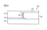
- FIG. 4shows a schematic illustration of a layer sequence 400 with carbon nanotubes which are contact-connected as via by means of two carbon interconnects.
- the layer sequence 400has a substrate 401 , on which a first carbon interconnect 402 is formed.
- a passivation layer 403is formed on said first carbon interconnect 401 .
- the passivation layer 403was patterned and a passage hole was formed, which uncovers a partial region of the first carbon interconnect 402 .
- carbon nanotubes 404which are shown schematically and not to scale in FIG. 4 , were then grown on the first carbon interconnect 401 by means of the known production processes, i.e. formation of a catalyst layer composed, for example, of iron, cobalt or nickel and growth thereon of the carbon nanotubes.
- the layer sequence 400has a second carbon interconnect 405 , which, like the first carbon interconnect 402 , makes contact with the carbon nanotubes 404 and was produced in the same way as the first carbon interconnect 402 by means of one of the processes explained with reference to FIG. 1 .
- one aspect of the inventioncan be seen in providing an electrical circuit with a nanostructure and a method for producing a contact-connection of a nanostructure, in particular a carbon nanostructure, which contact-connection has a low contact resistance.
- a so-called polycrystalline carbon layeris used for the contact-connection, which layer reduces the contact resistance, in particular the Schottky barrier, with respect to a nanostructure, particularly if the latter is formed as a carbon nanostructure, for example as a carbon nanotube.
- the method for producing the polycrystalline carbon layeris based on simple and customary process steps which are compatible with the use of a carbon nanostructure, that is to say that carbon nanostructures present are not destroyed during a subsequent process for forming the polycrystalline carbon layer.
- the specific conductivity of the polycrystalline carbonto be increased further by carrying out a doping or a so-called intercalation of the polycrystalline carbon.
Landscapes
- Engineering & Computer Science (AREA)
- Chemical & Material Sciences (AREA)
- Nanotechnology (AREA)
- Materials Engineering (AREA)
- Theoretical Computer Science (AREA)
- Crystallography & Structural Chemistry (AREA)
- Physics & Mathematics (AREA)
- Manufacturing & Machinery (AREA)
- Mathematical Physics (AREA)
- Internal Circuitry In Semiconductor Integrated Circuit Devices (AREA)
- Electrodes Of Semiconductors (AREA)
- Carbon And Carbon Compounds (AREA)
- Conductive Materials (AREA)
- Mobile Radio Communication Systems (AREA)
Abstract
Description
Claims (22)
Applications Claiming Priority (4)
| Application Number | Priority Date | Filing Date | Title |
|---|---|---|---|
| DE102004049453.3 | 2004-10-11 | ||
| DE102004049453ADE102004049453A1 (en) | 2004-10-11 | 2004-10-11 | Nanostructure electrical circuit and method of making a nanostructure contacting |
| DE102004049453 | 2004-10-11 | ||
| PCT/DE2005/001816WO2006039907A2 (en) | 2004-10-11 | 2005-10-11 | Electrical circuit with a nanostructure and method for contacting a nanostructure |
Publications (2)
| Publication Number | Publication Date |
|---|---|
| US20090213830A1 US20090213830A1 (en) | 2009-08-27 |
| US8664657B2true US8664657B2 (en) | 2014-03-04 |
Family
ID=35588904
Family Applications (1)
| Application Number | Title | Priority Date | Filing Date |
|---|---|---|---|
| US11/577,070Expired - Fee RelatedUS8664657B2 (en) | 2004-10-11 | 2005-10-11 | Electrical circuit with a nanostructure and method for producing a contact connection of a nanostructure |
Country Status (5)
| Country | Link |
|---|---|
| US (1) | US8664657B2 (en) |
| EP (1) | EP1800360B1 (en) |
| KR (1) | KR20070089912A (en) |
| DE (1) | DE102004049453A1 (en) |
| WO (1) | WO2006039907A2 (en) |
Cited By (1)
| Publication number | Priority date | Publication date | Assignee | Title |
|---|---|---|---|---|
| US20140162414A1 (en)* | 2012-12-12 | 2014-06-12 | Varian Semiconductor Equipment Associates, Inc. | Technique for selectively processing three dimensional device |
Families Citing this family (13)
| Publication number | Priority date | Publication date | Assignee | Title |
|---|---|---|---|---|
| DE102004049453A1 (en) | 2004-10-11 | 2006-04-20 | Infineon Technologies Ag | Nanostructure electrical circuit and method of making a nanostructure contacting |
| DE102004050393B4 (en)* | 2004-10-15 | 2010-09-16 | Infineon Technologies Ag | Communication device, control device and communication system |
| ES2336360T3 (en)* | 2006-04-20 | 2010-04-12 | Lifescan Scotland Ltd | METHOD FOR TRANSMITTING DATA IN A GLUCOSE SYSTEM IN BLOOD AND GLUCOSE SYSTEM IN BLOOD CORRESPONDING. |
| US20110061014A1 (en) | 2008-02-01 | 2011-03-10 | Energyhub | Interfacing to resource consumption management devices |
| US8255090B2 (en)* | 2008-02-01 | 2012-08-28 | Energyhub | System and method for home energy monitor and control |
| EP2507746B1 (en) | 2009-11-30 | 2015-10-14 | Corning Incorporated | Rfid condition latching |
| KR101179126B1 (en)* | 2010-03-31 | 2012-09-07 | 전자부품연구원 | magnetic field communication method for managing node with low power comsumption and the node operated thereby |
| US20120274452A1 (en)* | 2011-04-26 | 2012-11-01 | Aravind Chamarti | Radio frequency (rf)-enabled latches and related components, assemblies, systems, and methods |
| US9165232B2 (en) | 2012-05-14 | 2015-10-20 | Corning Incorporated | Radio-frequency identification (RFID) tag-to-tag autoconnect discovery, and related methods, circuits, and systems |
| US8624396B2 (en) | 2012-06-14 | 2014-01-07 | Taiwan Semiconductor Manufacturing Company, Ltd. | Apparatus and method for low contact resistance carbon nanotube interconnect |
| US9648612B2 (en) | 2013-12-23 | 2017-05-09 | At&T Intellectual Property I, L.P. | Method, computer-readable storage device, and apparatus for allocating timeslots on channels in a wireless network |
| US9974023B2 (en)* | 2015-09-25 | 2018-05-15 | Intel Corporation | Apparatus, system and method of communicating a wakeup packet |
| US11805483B2 (en)* | 2020-12-14 | 2023-10-31 | Marvell Asia Pte, Ltd. | Method and apparatus for restoring WUP mode for multi-speed ethernet device |
Citations (48)
| Publication number | Priority date | Publication date | Assignee | Title |
|---|---|---|---|---|
| US5940771A (en)* | 1991-05-13 | 1999-08-17 | Norand Corporation | Network supporting roaming, sleeping terminals |
| DE19856295A1 (en) | 1998-02-27 | 1999-09-09 | Fraunhofer Ges Forschung | Chemical field effect transistor with carbon gate electrode |
| US6280697B1 (en)* | 1999-03-01 | 2001-08-28 | The University Of North Carolina-Chapel Hill | Nanotube-based high energy material and method |
| US6325909B1 (en)* | 1999-09-24 | 2001-12-04 | The Governing Council Of The University Of Toronto | Method of growth of branched carbon nanotubes and devices produced from the branched nanotubes |
| WO2002011216A1 (en) | 2000-07-28 | 2002-02-07 | Infineon Technologies Ag | Field effect transistor, circuit arrangement and method for production of a field effect transistor |
| US6495258B1 (en)* | 2000-09-20 | 2002-12-17 | Auburn University | Structures with high number density of carbon nanotubes and 3-dimensional distribution |
| US20030008692A1 (en)* | 2001-07-05 | 2003-01-09 | Phelan John Roux | Energy conservation in battery powered tag |
| US20030143398A1 (en)* | 2000-02-25 | 2003-07-31 | Hiroshi Ohki | Carbon nanotube and method for producing the same, electron source and method for producing the same, and display |
| US6615033B1 (en)* | 2000-01-11 | 2003-09-02 | International Business Machines Corporation | Synchronized-timed-reminded communications for family radios |
| US6639907B2 (en)* | 2000-09-26 | 2003-10-28 | Qualcomm, Incorporated | Method and apparatus for processing paging indicator bits transmitted on a quick paging channel |
| US20040142172A1 (en)* | 2003-01-10 | 2004-07-22 | Sanyo Electric Co., Ltd. | Bonded structure including a carbon nanotube |
| US6798000B2 (en)* | 2000-07-04 | 2004-09-28 | Infineon Technologies Ag | Field effect transistor |
| US20040222081A1 (en)* | 2002-12-17 | 2004-11-11 | William Marsh Rice University | Use of microwaves to crosslink carbon nanotubes |
| US20040253996A1 (en)* | 2003-06-12 | 2004-12-16 | Industrial Technology Research Institute | Method and system for power-saving in a wireless local area network |
| US20040264397A1 (en)* | 2002-12-16 | 2004-12-30 | Mathilde Benveniste | Power-saving mechanism for periodic traffic streams in wireless local-area networks |
| EP1496554A2 (en) | 2003-07-07 | 2005-01-12 | Seiko Epson Corporation | Organic thin film transistor and method of manufacturing the same |
| US20050018624A1 (en)* | 2003-07-24 | 2005-01-27 | Meier Robert C. | Uniform power save method for 802.11e stations |
| US20050096101A1 (en)* | 2002-03-06 | 2005-05-05 | Sayers Anthony D. | Method to reduce power consumption in a radio communication system and apparatus therefor |
| US20050129573A1 (en)* | 2003-09-12 | 2005-06-16 | Nanomix, Inc. | Carbon dioxide nanoelectronic sensor |
| US20050233704A1 (en)* | 2004-04-16 | 2005-10-20 | Itaru Maekawa | Advanced power saving in communication terminal, communication system and power control method |
| US6972467B2 (en)* | 2002-08-23 | 2005-12-06 | Intel Corporation | Multi-gate carbon nano-tube transistors |
| US20050285116A1 (en)* | 2004-06-29 | 2005-12-29 | Yongqian Wang | Electronic assembly with carbon nanotube contact formations or interconnections |
| US6987302B1 (en)* | 2003-07-01 | 2006-01-17 | Yingjian Chen | Nanotube with at least a magnetic nanoparticle attached to the nanotube's exterior sidewall and electronic devices made thereof |
| WO2006039907A2 (en) | 2004-10-11 | 2006-04-20 | Qimonda Ag | Electrical circuit with a nanostructure and method for contacting a nanostructure |
| US7094692B2 (en)* | 2004-03-26 | 2006-08-22 | Fujitsu Limited | Semiconductor device and method of manufacturing the same |
| US20060226551A1 (en)* | 2001-05-02 | 2006-10-12 | Fujitsu Limited | Integrated circuit device and method of producing the same |
| US7183229B2 (en)* | 2000-12-08 | 2007-02-27 | Sony Corporation | Semiconductor thin film forming method, production methods for semiconductor device and electrooptical device, devices used for these methods, and semiconductor device and electrooptical device |
| US20070059947A1 (en)* | 2002-08-01 | 2007-03-15 | Semiconductor Energy Laboratory Co., Ltd. | Method of manufacturing carbon nanotube semiconductor device |
| US7245946B2 (en)* | 2003-07-07 | 2007-07-17 | Texas Instruments Incorporated | Optimal power saving scheduler for 802.11e APSD |
| US7247897B2 (en)* | 2003-05-01 | 2007-07-24 | Samsung Electronics Co., Ltd. | Conductive line for a semiconductor device using a carbon nanotube including a memory thin film and semiconductor device manufactured |
| US7335603B2 (en)* | 2000-02-07 | 2008-02-26 | Vladimir Mancevski | System and method for fabricating logic devices comprising carbon nanotube transistors |
| US20080053952A1 (en)* | 2003-12-26 | 2008-03-06 | Fuji Xerox Co., Ltd. | Rectifying Device, Electronic Circuit Using the Same, and Method of Manufacturing Rectifying Device |
| US20080159943A1 (en)* | 2003-09-17 | 2008-07-03 | Molecular Nanosystems, Inc. | Methods for synthesizing carbon nanotubes |
| US7400595B2 (en)* | 2003-06-17 | 2008-07-15 | Motorola, Inc. | Method and apparatus for battery life extension for nodes within beaconing networks |
| US20080179590A1 (en)* | 2000-02-07 | 2008-07-31 | Vladimir Mancevski | Logic devices comprising carbon nanotube patterns |
| US7413971B2 (en)* | 2001-12-13 | 2008-08-19 | Steinhoegl Werner | Method of producing a layered arrangement and layered arrangement |
| US7439081B2 (en)* | 2004-07-29 | 2008-10-21 | International Business Machines Corporation | Method for making integrated circuit chip utilizing oriented carbon nanotube conductive layers |
| US7452828B2 (en)* | 2003-05-30 | 2008-11-18 | Fuji Xerox Co., Ltd. | Carbon nanotube device, method of manufacturing the same, and carbon nanotube transfer body |
| US7507987B2 (en)* | 2002-10-11 | 2009-03-24 | Massachusetts Institute Of Technology | Method of making packets of nanostructures |
| US20090169951A1 (en)* | 2004-07-02 | 2009-07-02 | Kabushiki Kaisha Toshiba | Manufacturing methods of catalysts for carbon fiber composition and carbon material compound, manufacturing methods of carbon fiber and catalyst material for fuel cell, and catalyst material for fuel cell |
| US7573186B2 (en)* | 2003-12-15 | 2009-08-11 | Fuji Xerox Co., Ltd. | Electrode for electrochemical measurement |
| US7579272B2 (en)* | 2004-10-04 | 2009-08-25 | International Business Machines Corporation | Methods of forming low-k dielectric layers containing carbon nanostructures |
| US7801065B2 (en)* | 2003-11-25 | 2010-09-21 | Motorola Mobility, Inc. | Reception timing method and apparatus |
| US7829883B2 (en)* | 2004-02-12 | 2010-11-09 | International Business Machines Corporation | Vertical carbon nanotube field effect transistors and arrays |
| US7883968B2 (en)* | 2003-05-22 | 2011-02-08 | Fujitsu Limited | Field effect transistor and its manufacturing method |
| US20110159181A1 (en)* | 2004-02-18 | 2011-06-30 | Hitachi Metals, Ltd | Fine Composite Metal Particles and Their Production Method, Micro-Bodies, and Magnetic Beads |
| US20110162966A1 (en)* | 2003-02-27 | 2011-07-07 | Burke Peter J | Systems and methods for making and using nanoelectrodes |
| US20110212566A1 (en)* | 2003-06-06 | 2011-09-01 | Stmicroelectronics S.R.L. | Optically controlled electrical-switch device based upon carbon nanotubes and electrical-switch system using the switch device |
- 2004
- 2004-10-11DEDE102004049453Apatent/DE102004049453A1/ennot_activeWithdrawn
- 2005
- 2005-10-11WOPCT/DE2005/001816patent/WO2006039907A2/enactiveApplication Filing
- 2005-10-11KRKR1020077010783Apatent/KR20070089912A/ennot_activeCeased
- 2005-10-11USUS11/577,070patent/US8664657B2/ennot_activeExpired - Fee Related
- 2005-10-11EPEP05800840Apatent/EP1800360B1/ennot_activeCeased
Patent Citations (53)
| Publication number | Priority date | Publication date | Assignee | Title |
|---|---|---|---|---|
| US5940771A (en)* | 1991-05-13 | 1999-08-17 | Norand Corporation | Network supporting roaming, sleeping terminals |
| DE19856295A1 (en) | 1998-02-27 | 1999-09-09 | Fraunhofer Ges Forschung | Chemical field effect transistor with carbon gate electrode |
| US6280697B1 (en)* | 1999-03-01 | 2001-08-28 | The University Of North Carolina-Chapel Hill | Nanotube-based high energy material and method |
| US6325909B1 (en)* | 1999-09-24 | 2001-12-04 | The Governing Council Of The University Of Toronto | Method of growth of branched carbon nanotubes and devices produced from the branched nanotubes |
| US6615033B1 (en)* | 2000-01-11 | 2003-09-02 | International Business Machines Corporation | Synchronized-timed-reminded communications for family radios |
| US7335603B2 (en)* | 2000-02-07 | 2008-02-26 | Vladimir Mancevski | System and method for fabricating logic devices comprising carbon nanotube transistors |
| US20080179590A1 (en)* | 2000-02-07 | 2008-07-31 | Vladimir Mancevski | Logic devices comprising carbon nanotube patterns |
| US20030143398A1 (en)* | 2000-02-25 | 2003-07-31 | Hiroshi Ohki | Carbon nanotube and method for producing the same, electron source and method for producing the same, and display |
| US6798000B2 (en)* | 2000-07-04 | 2004-09-28 | Infineon Technologies Ag | Field effect transistor |
| US6740910B2 (en) | 2000-07-28 | 2004-05-25 | Infineon Technologies Ag | Field-effect transistor, circuit configuration and method of fabricating a field-effect transistor |
| WO2002011216A1 (en) | 2000-07-28 | 2002-02-07 | Infineon Technologies Ag | Field effect transistor, circuit arrangement and method for production of a field effect transistor |
| US6495258B1 (en)* | 2000-09-20 | 2002-12-17 | Auburn University | Structures with high number density of carbon nanotubes and 3-dimensional distribution |
| US6639907B2 (en)* | 2000-09-26 | 2003-10-28 | Qualcomm, Incorporated | Method and apparatus for processing paging indicator bits transmitted on a quick paging channel |
| US20070087492A1 (en)* | 2000-12-08 | 2007-04-19 | Hideo Yamanaka | Method for forming semiconductor film, method for manufacturing semiconductor device and electrooptic device, apparatus for performing the same, and semiconductor device and electrooptic device |
| US7183229B2 (en)* | 2000-12-08 | 2007-02-27 | Sony Corporation | Semiconductor thin film forming method, production methods for semiconductor device and electrooptical device, devices used for these methods, and semiconductor device and electrooptical device |
| US20060226551A1 (en)* | 2001-05-02 | 2006-10-12 | Fujitsu Limited | Integrated circuit device and method of producing the same |
| US7332810B2 (en)* | 2001-05-02 | 2008-02-19 | Fujitsu Limited | Integrated circuit device and method of producing the same |
| US20030008692A1 (en)* | 2001-07-05 | 2003-01-09 | Phelan John Roux | Energy conservation in battery powered tag |
| US7413971B2 (en)* | 2001-12-13 | 2008-08-19 | Steinhoegl Werner | Method of producing a layered arrangement and layered arrangement |
| US20050096101A1 (en)* | 2002-03-06 | 2005-05-05 | Sayers Anthony D. | Method to reduce power consumption in a radio communication system and apparatus therefor |
| US20070059947A1 (en)* | 2002-08-01 | 2007-03-15 | Semiconductor Energy Laboratory Co., Ltd. | Method of manufacturing carbon nanotube semiconductor device |
| US7560756B2 (en)* | 2002-08-23 | 2009-07-14 | Intel Corporation | Tri-gate devices and methods of fabrication |
| US6972467B2 (en)* | 2002-08-23 | 2005-12-06 | Intel Corporation | Multi-gate carbon nano-tube transistors |
| US7507987B2 (en)* | 2002-10-11 | 2009-03-24 | Massachusetts Institute Of Technology | Method of making packets of nanostructures |
| US20040264397A1 (en)* | 2002-12-16 | 2004-12-30 | Mathilde Benveniste | Power-saving mechanism for periodic traffic streams in wireless local-area networks |
| US20040222081A1 (en)* | 2002-12-17 | 2004-11-11 | William Marsh Rice University | Use of microwaves to crosslink carbon nanotubes |
| US20040142172A1 (en)* | 2003-01-10 | 2004-07-22 | Sanyo Electric Co., Ltd. | Bonded structure including a carbon nanotube |
| US20110162966A1 (en)* | 2003-02-27 | 2011-07-07 | Burke Peter J | Systems and methods for making and using nanoelectrodes |
| US7247897B2 (en)* | 2003-05-01 | 2007-07-24 | Samsung Electronics Co., Ltd. | Conductive line for a semiconductor device using a carbon nanotube including a memory thin film and semiconductor device manufactured |
| US7883968B2 (en)* | 2003-05-22 | 2011-02-08 | Fujitsu Limited | Field effect transistor and its manufacturing method |
| US7452828B2 (en)* | 2003-05-30 | 2008-11-18 | Fuji Xerox Co., Ltd. | Carbon nanotube device, method of manufacturing the same, and carbon nanotube transfer body |
| US20110212566A1 (en)* | 2003-06-06 | 2011-09-01 | Stmicroelectronics S.R.L. | Optically controlled electrical-switch device based upon carbon nanotubes and electrical-switch system using the switch device |
| US20040253996A1 (en)* | 2003-06-12 | 2004-12-16 | Industrial Technology Research Institute | Method and system for power-saving in a wireless local area network |
| US7400595B2 (en)* | 2003-06-17 | 2008-07-15 | Motorola, Inc. | Method and apparatus for battery life extension for nodes within beaconing networks |
| US6987302B1 (en)* | 2003-07-01 | 2006-01-17 | Yingjian Chen | Nanotube with at least a magnetic nanoparticle attached to the nanotube's exterior sidewall and electronic devices made thereof |
| US7329897B2 (en) | 2003-07-07 | 2008-02-12 | Seiko Epson Corporation | Organic thin film transistor and method of manufacturing the same |
| US7245946B2 (en)* | 2003-07-07 | 2007-07-17 | Texas Instruments Incorporated | Optimal power saving scheduler for 802.11e APSD |
| EP1496554A2 (en) | 2003-07-07 | 2005-01-12 | Seiko Epson Corporation | Organic thin film transistor and method of manufacturing the same |
| US20050018624A1 (en)* | 2003-07-24 | 2005-01-27 | Meier Robert C. | Uniform power save method for 802.11e stations |
| US20050129573A1 (en)* | 2003-09-12 | 2005-06-16 | Nanomix, Inc. | Carbon dioxide nanoelectronic sensor |
| US20080159943A1 (en)* | 2003-09-17 | 2008-07-03 | Molecular Nanosystems, Inc. | Methods for synthesizing carbon nanotubes |
| US7801065B2 (en)* | 2003-11-25 | 2010-09-21 | Motorola Mobility, Inc. | Reception timing method and apparatus |
| US7573186B2 (en)* | 2003-12-15 | 2009-08-11 | Fuji Xerox Co., Ltd. | Electrode for electrochemical measurement |
| US20080053952A1 (en)* | 2003-12-26 | 2008-03-06 | Fuji Xerox Co., Ltd. | Rectifying Device, Electronic Circuit Using the Same, and Method of Manufacturing Rectifying Device |
| US7829883B2 (en)* | 2004-02-12 | 2010-11-09 | International Business Machines Corporation | Vertical carbon nanotube field effect transistors and arrays |
| US20110159181A1 (en)* | 2004-02-18 | 2011-06-30 | Hitachi Metals, Ltd | Fine Composite Metal Particles and Their Production Method, Micro-Bodies, and Magnetic Beads |
| US7094692B2 (en)* | 2004-03-26 | 2006-08-22 | Fujitsu Limited | Semiconductor device and method of manufacturing the same |
| US20050233704A1 (en)* | 2004-04-16 | 2005-10-20 | Itaru Maekawa | Advanced power saving in communication terminal, communication system and power control method |
| US20050285116A1 (en)* | 2004-06-29 | 2005-12-29 | Yongqian Wang | Electronic assembly with carbon nanotube contact formations or interconnections |
| US20090169951A1 (en)* | 2004-07-02 | 2009-07-02 | Kabushiki Kaisha Toshiba | Manufacturing methods of catalysts for carbon fiber composition and carbon material compound, manufacturing methods of carbon fiber and catalyst material for fuel cell, and catalyst material for fuel cell |
| US7439081B2 (en)* | 2004-07-29 | 2008-10-21 | International Business Machines Corporation | Method for making integrated circuit chip utilizing oriented carbon nanotube conductive layers |
| US7579272B2 (en)* | 2004-10-04 | 2009-08-25 | International Business Machines Corporation | Methods of forming low-k dielectric layers containing carbon nanostructures |
| WO2006039907A2 (en) | 2004-10-11 | 2006-04-20 | Qimonda Ag | Electrical circuit with a nanostructure and method for contacting a nanostructure |
Non-Patent Citations (8)
| Title |
|---|
| A. Javey et al., "Ballistic Carbon Nanotube Field-Effect Transistors", Nature, vol. 424 (Aug. 2003) pp. 654-657. |
| Graham et al., "Towards the integration of carbon nanotubes in microelectronics", Diamond and Related Materials, vol. 13, Apr.-Aug. 2004, pp. 1296-1300. |
| Hung et al., "Growth and Analysis of Polycrystalline Carbon for MOS Applications", Material Research Society Symposium Proceedings, vol. 427, 1996, pp. 317-322. |
| M. Nihei et al., "Simultaneous Formation of Multiwall Carbon Nanotubes and their End-Bonded Ohmic Contacts to Ti Electrodes for Future ULSI Interconnects", Japanese Journal of Applied Physics, vol. 43, No. 4B, Apr. 2004, pp. 1856-1859. |
| R. Martel et al., "Ambipolar Electrical Transport in Semiconducting Single-Wall Carbon Nanotubes", Physical Review Letters, vol. 87, No. 25 (2001). |
| S. Heinze et al., "Carbon Nanotubes as Schottky Barrier Transistors", Physical Review Letters, vol. 89, No. 10 (2002). |
| W. Yu et al., "Spinose carbon nanotubes grown on graphitized DLC film by low frequency r.f. plasma-enhanced chemical vapor deposition", Diamond and Related Materials, vol. 12, No. 12, Dec. 2003, pp. 2203-2207. |
| X. Sun et al., "Growth of carbon nanotubes on carbon paper by Ohmically heating silane-dispersed catalytic sites", Chemical Physics Letters, vol. 363, No. 5-6, Sep. 16, 2002, pp. 415-421. |
Cited By (2)
| Publication number | Priority date | Publication date | Assignee | Title |
|---|---|---|---|---|
| US20140162414A1 (en)* | 2012-12-12 | 2014-06-12 | Varian Semiconductor Equipment Associates, Inc. | Technique for selectively processing three dimensional device |
| US9337314B2 (en)* | 2012-12-12 | 2016-05-10 | Varian Semiconductor Equipment Associates, Inc. | Technique for selectively processing three dimensional device |
Also Published As
| Publication number | Publication date |
|---|---|
| US20090213830A1 (en) | 2009-08-27 |
| WO2006039907A2 (en) | 2006-04-20 |
| EP1800360B1 (en) | 2012-02-22 |
| DE102004049453A1 (en) | 2006-04-20 |
| EP1800360A2 (en) | 2007-06-27 |
| KR20070089912A (en) | 2007-09-04 |
| WO2006039907A3 (en) | 2006-06-22 |
Similar Documents
| Publication | Publication Date | Title |
|---|---|---|
| Graham et al. | How do carbon nanotubes fit into the semiconductor roadmap? | |
| Chung et al. | Silicon nanowire devices | |
| US8664657B2 (en) | Electrical circuit with a nanostructure and method for producing a contact connection of a nanostructure | |
| US7341774B2 (en) | Electronic and opto-electronic devices fabricated from nanostructured high surface to volume ratio thin films | |
| US7709827B2 (en) | Vertically integrated field-effect transistor having a nanostructure therein | |
| US7084507B2 (en) | Integrated circuit device and method of producing the same | |
| JP5511746B2 (en) | Method for forming vertical nanotube semiconductor device structure | |
| CN1886332A (en) | Method of sorting carbon nanotubes | |
| US7872334B2 (en) | Carbon nanotube diodes and electrostatic discharge circuits and methods | |
| CN1838446A (en) | Self-contained electrostatically doped carbon nanotube device and manufacturing method thereof | |
| US20070155064A1 (en) | Method for manufacturing carbon nano-tube FET | |
| US20240014071A1 (en) | Cmos-compatible graphene structures, interconnects and fabrication methods | |
| US20140287575A1 (en) | Spatial orientation of the carbon nanotubes in electrophoretic deposition process | |
| US7553472B2 (en) | Nanotube forming methods | |
| CN1770467A (en) | Unipolar nanotube transistor using carrier-trapping material and method of manufacturing the same | |
| Chai et al. | Nanodiode based on a multiwallCNx/carbon nanotube intramolecular junction | |
| CN1992198A (en) | Carbon nano-tube generating method and method for forming electric wire of semiconductor device | |
| Tang et al. | High-performance carbon nanotube complementary logic with end-bonded contacts | |
| JP4935808B2 (en) | Carbon nanotube device and manufacturing method thereof | |
| US20100068828A1 (en) | Method of forming a structure having a giant resistance anisotropy or low-k dielectric | |
| KR100873800B1 (en) | Silicide Forming Method of Semiconductor Device Using Carbon Nanotubes | |
| KR101010115B1 (en) | Semiconductor element and method of forming the same | |
| Graham et al. | Towards the integration of carbon nanotubes in microelectronics | |
| JP2003142679A (en) | Optoelectronic integrated circuit device | |
| CN116631957A (en) | Semiconductor device based on encapsulated graphene nanoribbons and preparation method thereof |
Legal Events
| Date | Code | Title | Description |
|---|---|---|---|
| AS | Assignment | Owner name:QIMONDA AG, GERMANY Free format text:ASSIGNMENT OF ASSIGNORS INTEREST;ASSIGNORS:DUESBERG, GEORG;KREUPL, FRANZ;SEIDEL, ROBERT;AND OTHERS;REEL/FRAME:022298/0521;SIGNING DATES FROM 20070523 TO 20070828 Owner name:QIMONDA AG, GERMANY Free format text:ASSIGNMENT OF ASSIGNORS INTEREST;ASSIGNORS:DUESBERG, GEORG;KREUPL, FRANZ;SEIDEL, ROBERT;AND OTHERS;SIGNING DATES FROM 20070523 TO 20070828;REEL/FRAME:022298/0521 | |
| AS | Assignment | Owner name:QIMONDA AG, GERMANY Free format text:RE-RECORD TO CORRECT THE ADDRESS OF THE ASSIGNEE, PREVIOUSLY RECORDED ON REEL 022298 FRAME 0521.;ASSIGNORS:DUESBERG, GEORG;KREUPL, FRANZ;SEIDEL, ROBERT;AND OTHERS;REEL/FRAME:023317/0169;SIGNING DATES FROM 20070523 TO 20070828 Owner name:QIMONDA AG, GERMANY Free format text:RE-RECORD TO CORRECT THE ADDRESS OF THE ASSIGNEE, PREVIOUSLY RECORDED ON REEL 022298 FRAME 0521;ASSIGNORS:DUESBERG, GEORG;KREUPL, FRANZ;SEIDEL, ROBERT;AND OTHERS;SIGNING DATES FROM 20070523 TO 20070828;REEL/FRAME:023317/0169 | |
| FEPP | Fee payment procedure | Free format text:PAYOR NUMBER ASSIGNED (ORIGINAL EVENT CODE: ASPN); ENTITY STATUS OF PATENT OWNER: LARGE ENTITY | |
| AS | Assignment | Owner name:INFINEON TECHNOLOGIES AG, GERMANY Free format text:ASSIGNMENT OF ASSIGNORS INTEREST;ASSIGNOR:QIMONDA AG;REEL/FRAME:035623/0001 Effective date:20141009 | |
| AS | Assignment | Owner name:POLARIS INNOVATIONS LIMITED, IRELAND Free format text:ASSIGNMENT OF ASSIGNORS INTEREST;ASSIGNOR:INFINEON TECHNOLOGIES AG;REEL/FRAME:036908/0923 Effective date:20150708 | |
| FEPP | Fee payment procedure | Free format text:MAINTENANCE FEE REMINDER MAILED (ORIGINAL EVENT CODE: REM.) | |
| LAPS | Lapse for failure to pay maintenance fees | Free format text:PATENT EXPIRED FOR FAILURE TO PAY MAINTENANCE FEES (ORIGINAL EVENT CODE: EXP.) | |
| STCH | Information on status: patent discontinuation | Free format text:PATENT EXPIRED DUE TO NONPAYMENT OF MAINTENANCE FEES UNDER 37 CFR 1.362 | |
| FP | Lapsed due to failure to pay maintenance fee | Effective date:20180304 |