US8661527B2 - Authenticator, authenticatee and authentication method - Google Patents
Authenticator, authenticatee and authentication methodDownload PDFInfo
- Publication number
- US8661527B2 US8661527B2US13/486,684US201213486684AUS8661527B2US 8661527 B2US8661527 B2US 8661527B2US 201213486684 AUS201213486684 AUS 201213486684AUS 8661527 B2US8661527 B2US 8661527B2
- Authority
- US
- United States
- Prior art keywords
- information
- data
- nand flash
- flash memory
- host device
- Prior art date
- Legal status (The legal status is an assumption and is not a legal conclusion. Google has not performed a legal analysis and makes no representation as to the accuracy of the status listed.)
- Active
Links
Images


Classifications
- H—ELECTRICITY
- H04—ELECTRIC COMMUNICATION TECHNIQUE
- H04L—TRANSMISSION OF DIGITAL INFORMATION, e.g. TELEGRAPHIC COMMUNICATION
- H04L9/00—Cryptographic mechanisms or cryptographic arrangements for secret or secure communications; Network security protocols
- H04L9/08—Key distribution or management, e.g. generation, sharing or updating, of cryptographic keys or passwords
- H04L9/0861—Generation of secret information including derivation or calculation of cryptographic keys or passwords
- H04L9/0869—Generation of secret information including derivation or calculation of cryptographic keys or passwords involving random numbers or seeds
- G—PHYSICS
- G06—COMPUTING OR CALCULATING; COUNTING
- G06F—ELECTRIC DIGITAL DATA PROCESSING
- G06F21/00—Security arrangements for protecting computers, components thereof, programs or data against unauthorised activity
- G06F21/30—Authentication, i.e. establishing the identity or authorisation of security principals
- G06F21/31—User authentication
- G06F21/34—User authentication involving the use of external additional devices, e.g. dongles or smart cards
- G—PHYSICS
- G06—COMPUTING OR CALCULATING; COUNTING
- G06F—ELECTRIC DIGITAL DATA PROCESSING
- G06F21/00—Security arrangements for protecting computers, components thereof, programs or data against unauthorised activity
- G06F21/60—Protecting data
- G06F21/62—Protecting access to data via a platform, e.g. using keys or access control rules
- G06F21/6218—Protecting access to data via a platform, e.g. using keys or access control rules to a system of files or objects, e.g. local or distributed file system or database
- H—ELECTRICITY
- H04—ELECTRIC COMMUNICATION TECHNIQUE
- H04L—TRANSMISSION OF DIGITAL INFORMATION, e.g. TELEGRAPHIC COMMUNICATION
- H04L9/00—Cryptographic mechanisms or cryptographic arrangements for secret or secure communications; Network security protocols
- H04L9/08—Key distribution or management, e.g. generation, sharing or updating, of cryptographic keys or passwords
- H04L9/0816—Key establishment, i.e. cryptographic processes or cryptographic protocols whereby a shared secret becomes available to two or more parties, for subsequent use
- H—ELECTRICITY
- H04—ELECTRIC COMMUNICATION TECHNIQUE
- H04L—TRANSMISSION OF DIGITAL INFORMATION, e.g. TELEGRAPHIC COMMUNICATION
- H04L9/00—Cryptographic mechanisms or cryptographic arrangements for secret or secure communications; Network security protocols
- H04L9/14—Cryptographic mechanisms or cryptographic arrangements for secret or secure communications; Network security protocols using a plurality of keys or algorithms
- H—ELECTRICITY
- H04—ELECTRIC COMMUNICATION TECHNIQUE
- H04L—TRANSMISSION OF DIGITAL INFORMATION, e.g. TELEGRAPHIC COMMUNICATION
- H04L9/00—Cryptographic mechanisms or cryptographic arrangements for secret or secure communications; Network security protocols
- H04L9/32—Cryptographic mechanisms or cryptographic arrangements for secret or secure communications; Network security protocols including means for verifying the identity or authority of a user of the system or for message authentication, e.g. authorization, entity authentication, data integrity or data verification, non-repudiation, key authentication or verification of credentials
- H04L9/3271—Cryptographic mechanisms or cryptographic arrangements for secret or secure communications; Network security protocols including means for verifying the identity or authority of a user of the system or for message authentication, e.g. authorization, entity authentication, data integrity or data verification, non-repudiation, key authentication or verification of credentials using challenge-response
- H—ELECTRICITY
- H04—ELECTRIC COMMUNICATION TECHNIQUE
- H04L—TRANSMISSION OF DIGITAL INFORMATION, e.g. TELEGRAPHIC COMMUNICATION
- H04L2209/00—Additional information or applications relating to cryptographic mechanisms or cryptographic arrangements for secret or secure communication H04L9/00
- H04L2209/16—Obfuscation or hiding, e.g. involving white box
- H—ELECTRICITY
- H04—ELECTRIC COMMUNICATION TECHNIQUE
- H04L—TRANSMISSION OF DIGITAL INFORMATION, e.g. TELEGRAPHIC COMMUNICATION
- H04L2209/00—Additional information or applications relating to cryptographic mechanisms or cryptographic arrangements for secret or secure communication H04L9/00
- H04L2209/24—Key scheduling, i.e. generating round keys or sub-keys for block encryption
Definitions
- Embodiments described hereinrelate generally to an authenticator, an authenticatee and an authentication method.
- an ID and secret information for individualizing the IC cardare stored in an IC in the card, and the IC card has a cipher processing function for executing authentication based on the ID and secret information.
- an authentication methodis specified in Content Protection for Recordable Media (CPRM) as means for certifying authenticity of an SD (registered trademark) card in protection of copyrighted contents.
- CPRMContent Protection for Recordable Media
- an imitative SD (registered trademark) card in disguiseis produced by using hidden information extracted from software, thereby to deceitfully use an authentic software player.
- a false SD (registered trademark) cardis produced such that an encryption key, which was used in encryption of content, can be easily read out from the false SD (registered trademark) card. Thereby, it becomes possible to easily decode the video content recorded in the false SD (registered trademark) card, by using an authentic video recorder.
- An authenticatormay be provided not only as a dedicated hardware device such as a consumer device, but also as a program (software) which is executable in a PC (personal computer) or the like, and, in some cases, the software functions as a substantial authenticator.
- an authenticateeis, for instance, recording media or the like.
- a program called “firmware”mediates in the operation of hardware which constitutes the recording media, an important process or information is stored in a hidden state in hardware in the cell array.
- the tamper-resistancethe resistance to attacks
- FIG. 1is a block diagram showing a structure example of a memory system according to a first embodiment
- FIG. 2is a flow chart illustrating an authentication flow of the memory system according to the first embodiment
- FIG. 3is a view illustrating a structure example of a Set of Encrypted LotID set (SELID) in the first embodiment
- FIG. 4is a block diagram illustrating a structure example of a memory system according to a second embodiment
- FIG. 5is a flow chart illustrating an authentication flow of the memory system according to the second embodiment
- FIG. 6is a view illustrating a structure example of a Set of Encrypted LotID set (SELID) in the second embodiment
- FIG. 7is a block diagram illustrating a structure example of a memory system according to a third embodiment
- FIG. 8is a flow chart illustrating an authentication flow of the memory system according to the third embodiment.
- FIG. 9is a block diagram illustrating a structure example of a memory system according to a fourth embodiment.
- FIG. 10is a flow chart illustrating an authentication flow of the memory system according to the fourth embodiment.
- FIG. 11is a block diagram illustrating a structure example of a memory system according to a fifth embodiment
- FIG. 12is a flow chart illustrating an authentication flow of the memory system according to the fifth embodiment.
- FIG. 13is a block diagram illustrating a structure example of a memory system according to a sixth embodiment
- FIG. 14is a flow chart illustrating an authentication flow of the memory system according to the sixth embodiment.
- FIG. 15is a block diagram illustrating a structure example of a memory system according to a seventh embodiment
- FIG. 16is a flow chart illustrating an authentication flow of the memory system according to the seventh embodiment.
- FIG. 17is a view illustrating a structure example of a Set of Encrypted LotID set (SELID) in the seventh embodiment
- FIG. 18is a block diagram illustrating a structure example of a memory system according to an eighth embodiment.
- FIG. 19is a flow chart illustrating an authentication flow of the memory system according to the eighth embodiment.
- FIG. 20is a view illustrating a structure example of a Set of Encrypted ChipID set (SECID) in the eighth embodiment
- FIG. 21is a block diagram illustrating a structure example of a memory system according to a ninth embodiment.
- FIG. 22is a flow chart illustrating an authentication flow of the memory system according to the ninth embodiment.
- FIG. 23is a view illustrating a structure example of a Set of Encrypted ChipID set (SECID) in the ninth embodiment
- FIG. 24is a block diagram illustrating a structure example of a memory system according to a tenth embodiment
- FIG. 25is a flow chart illustrating an authentication flow of the memory system according to the tenth embodiment.
- FIG. 26is a block diagram illustrating a structure example of a memory system according to an eleventh embodiment
- FIG. 27is a flow chart illustrating an authentication flow of the memory system according to the eleventh embodiment.
- FIG. 28is a block diagram illustrating a structure example of a memory system according to a twelfth embodiment
- FIG. 29is a view showing an authenticatee in a state prior to SECID write in the twelfth embodiment
- FIG. 30is a block diagram illustrating a system of downloading the SECID in the twelfth embodiment
- FIG. 31is a flow chart illustrating a flow of downloading the SECID in the twelfth embodiment
- FIG. 32is a block diagram illustrating a memory system according to a 13th embodiment
- FIG. 33is a block diagram showing a NAND flash memory according to a 14th embodiment.
- FIG. 34is an equivalent circuit diagram showing a block (BLOCK) in the 14th embodiment.
- an authenticator which authenticates an authenticatee, which stores first key information (NKey) that is hiddenincludes a memory configured to store second key information (HKey) which is hidden; a random number generation module configured to generate random number information; and a data generation module configured to generate a session key (SKey) by using the second key information (HKey) and the random number information.
- the authenticatoris configured such that the second key information (HKey) is generated from the first key information (NKey) but the first key information (NKey) is not generated from the second key information (HKey).
- FIG. 1a structure example of a memory system according to the first embodiment is described.
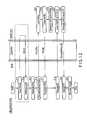
- the memory systemincludes a NAND flash memory 10 which is an authenticatee, a host device 20 which is an authenticator, and a controller 19 which mediates between both.
- the host device 20accesses the NAND flash memory 10 via the controller 19 .
- a fabrication process of a semiconductor productsuch as NAND flash memory 10 , is described in brief.
- the fabrication process of a semiconductor productis mainly divided into a pre-process of forming a circuit on a substrate wafer, and a post-process of dicing the wafer into pieces and performing wiring and resin package sealing.
- the controller 19is variously configured, for example, such that the controller 19 is included in the NAND flash memory 10 in the pre-process, the controller 19 is not included in the pre-process but is included in the same package in the post-process, or the controller 19 is formed as a chip which is different from the NAND flash memory 10 .
- the controller 19is formed as a chip different from the NAND flash memory 10 .
- the controller 19mediates, in many cases, in the transactions of data and instructions between the host device 20 and NAND flash memory 10 . Even in this case, the controller 19 does not change the substantial contents of the above-described data and instructions, so a description of the details will be omitted in some cases. Structure examples of the NAND flash memory 10 and controller 19 will be described later in detail.
- the host device 20is constructed by dedicated hardware, like a consumer device, it is thinkable that the host device 20 is composed of a combination of dedicated hardware and firmware that operates the hardware, and that the function of the device is constructed by a software program which operates on the PC.
- This embodimentillustrates a method of reading out identification information, such as ChipID or LotID, which is recorded in the NAND flash memory 10 that is the authenticatee, in the state in which the identification information is hidden from a third party, and surely confirming the data that is read out from the authenticatee 10 , and shows a structure example in the case where this method is applied to the NAND flash memory 10 .
- identification informationsuch as ChipID or LotID
- the NAND flash memory 10includes a cell array 11 , a data cache 12 which is disposed in a peripheral area of the cell array 11 , data generation modules (Generate) 13 and 16 , a data concatenation module (Concatenate) 14 , a random number generator (RNG) 15 , an exclusive-OR module (EXOR) 17 , and an encryptor (Encrypt) 18 .
- a plurality of memory cellsare arranged in a matrix at intersections between bit lines and word lines (not shown).
- the memory cellincludes, in the named order on a semiconductor substrate, a tunnel insulation film, a floating gate, an interlayer insulation film, and a control gate connected to the word line.
- Current paths of memory cells in the bit line directionare connected in series, thereby constituting a cell unit.
- the cell unitis selected by a select transistor which is connected to the bit line and a source line.
- a plurality of memory cells in the word line directionconstitute 1 page (Page) which is a unit of data read and data write.
- a plurality of pagesconstitutes a block (Block) which is a unit of data erase.
- the cell array (Cell array) 11includes a user area (User area) 11 - 1 , a hidden area (Hidden area) 11 - 2 and a ROM area (ROM area) 11 - 3 .
- the user area (User area) 11 - 1is an area in which data write and data read can be freely executed.
- SELIDSet of Encrypted LotID
- content datasuch as photos, video, music or e-books, are recorded in the user area 11 - 1 .
- the structure of the SELID in this embodimentwill be described later with reference to FIG. 3 .
- the hidden area (Hidden area) 11 - 2is an area in which the outside of the NAND flash memory 10 is prohibited from data write, and in which data read is prohibited (Read/Program inhibit).
- NKeyfirst key information
- second key information (HKey)is generated from the first key information (NKey).
- NKeysecond key information
- such configurationis adopted that the first key information (NKey) cannot be generated from the second key information (HKey).
- the ROM area (ROM area) 11 - 3is an area in which data write from the outside is prohibited and data read from the outside is permitted.
- a chip ID (ChipID) and a lot ID (LotID), which are identification information,are recorded.
- ChipID and LotIDare recorded, in general, in the state in which the ChipID and LotID are error-correction-encoded, so that the correct identification information may be read out even when an error has occurred in the data.
- the error-correction encoding/decodingis not particularly illustrated.
- the chip ID (ChipID)is a unique ID which is allocated to the NAND flash memory 10 on a chip-by-chip basis.
- the lot IDis an ID which is allocated to each group of a certain number of chips in the manufacturing process of NAND flash memories 10 .
- the LotIDis changed between groups each comprising a predetermined number of chips, e.g. one million chips, or the LotID is changed at predetermined time intervals of manufacture, such as one month or a half year.
- the ChipID and LotIDmay be recorded in the above-described hidden area, in place of the ROM area.
- the above-described ROM area 11 - 3 , hidden area 11 - 2 and user area 11 - 1may be realized by making physical structures different, or may be realized by logical control within the NAND flash memory 10 , with the physical structure being the same.
- the logical controlis, for example, such a method that the respective areas are provided with identifiers which control access from the outside of the NAND flash memory 10 , these identifiers are stored, and access control is executed by the identifiers when the NAND flash memory 10 has accepted access to the areas from the outside.
- each of the memory cells constituting the cell array (Cell array) 11may be a memory cell which stores a plurality of bits (MLC: Multi Level Cell) or a memory cell which stores 1 bit (SLC: Single Level Cell).
- MLCMulti Level Cell
- SLCSingle Level Cell
- the ROM area 11 - 3 and hidden area 11 - 2may be configured to be used by the SLC
- the user area 11 - 1may be configured to be used by the MLC.
- the physical structure of the cell arraymay be different between the SLC area and the MLC area, or only partial bits of the memory cell, which is usable as the MCL, may be utilized as a pseudo-SLC area.
- the data cache (Data cache) 12temporarily stores data which has been read out from the cell array 11 .
- Each of the data generation modules (Generate) 13 , 16is a module which generates output data by a predetermined calculation from a plurality of input data.
- the data generation module 13converts information (HC j ), which has been received from the host device 20 , by using the above-described first secret information NKey, thereby generating HKey j (second key information). In this manner, on the NAND flash memory 10 side, the second key information (HKey j ) can be generated from the first key information (NKey).
- the data generation module 16converts, by using the HKey j , data which is created by concatenating a random number RN h , which has been received from the host device 20 , and a random number RN c , which has been generated by the NAND flash memory 10 itself, thereby generating a session key SKey j .
- AESAdvanced Encryption Standard
- encryptorsmay be used for the data generation modules 13 and 16 .
- each of the data generation modules (Generate) 13 , 16is a module which outputs new data from plural input information pieces.
- the two data generation modules 13 and 16which are depicted as different structural elements in order to make the data processing procedure easy to understand, may be realized by repeatedly utilizing the same module.
- the data concatenation module (Concatenate) 14concatenates two input data (random number RN h , random number RN c ) and outputs the concatenated data to the data generation circuit 16 .
- the random number generator (RNG) 15generates a random number RN c , which is used for authentication.
- the exclusive-OR module (EXOR) 17receives, as input data, two identification information pieces (ChipID, LotID) which are read out of the ROM area 11 - 3 , calculates an exclusive logical sum of the two input data, and outputs the calculation result.
- the identification informationis stored in the hidden area in place of the ROM area, as described above, the identification information, which is the input data to the exclusive-OR module, is read out of the hidden area.
- the encryptor (Encrypt) 18is a module which encrypts the input data by key data which is input separately, and outputs encrypted input data.
- the encryptor 18may also be used as the data generation module. In this case, (+) represents exclusive logical addition.
- an output module for outputting datawhich is to be sent to the host device 20 via the controller 19 , is actually disposed as a structural element.
- the structural elementssuch as the data cache 12 , other than the cell array 11 , may also be disposed in the memory controller (Controller) 19 .
- the host device 20includes a memory (Memory) 23 , a random number generator (RNG) 25 , a data concatenation module (Concatenate) 26 , exclusive-OR modules (EXOR) 24 and 29 , a data selector (Select) 21 , a data generator (Generate) 27 , and decryptors (Decrypt) 22 and 28 .
- the memory (Memory) 23stores secret information HKey j and a host constant HC j , which are necessary for executing the authentication process of the present embodiment.
- the secret information HKey jneeds to be stored by using such means as to prevent exposure to the outside.
- the host devicesuch as a consumer device, which is constructed by using dedicated hardware
- the secret information HKey jcan securely be protected by protecting the program itself by using a tamper-resistant software technology.
- the random number generator (RNG) 25generates RN h which is used for authentication.
- the data concatenation module (Concatenate) 26concatenates two input random number data (RN h , RN c ) which are generated by the random number generators 15 and 25 , and outputs the concatenated data.
- Each of the exclusive-OR modules (EXOR) 24 and 29calculates an exclusive logical sum of two input data, and outputs the calculation result.
- the data selector (Select) 21selects, by using index information j of secret information HKey j , encrypted LotID data which can be decrypted by using the secret information HKey j that is hidden in the host device 20 , from the set of encrypted LotID (SELID) which has been read out of the NAND flash memory 10 .
- the secret information HKey jis recorded in an internal dedicated memory after being encrypted by a unique method of the manufacturer.
- the secret information HKey jis stored in the state in which the secret information HKey j can be protected against unlawful analysis by a tamper-resistant software (TRS) technology.
- TRStamper-resistant software
- the secret information HKey jis stored, after taking such a measure as hiding the secret information HKey j by using the function of the security module.
- the data generator (Generate) 27is an arithmetic module which generates output data by a predetermined calculation from a plurality of input data.
- the data generator (Generate) 27executes the same calculation process as the data generation module 16 which is provided in the NAND flash memory.
- the data generator 27 in this exampleconverts, by using the secret information HKey j hidden in the host device 20 , data which is created by concatenating the random number RN h , which has been generated by the host device 20 itself, and the random number RN c , which has been received from the NAND flash memory 10 , thereby generating a session key SKey j .
- the data generator 27can use, for example, an AES encryption calculation.
- the decryptor (Decrypt) 22 , 28decrypts input data by key data which is separately input, and outputs decrypted input data.
- the decryptor 22is used in order to obtain LotID by decrypting encrypted LotID data which has been selected by the data selector 21 , by using, as key information, a calculation result by the exclusive-OR module with respect to the secret information HKey j hidden in the host device and index information j for identifying the secret information HKey j , where necessary.
- the decryptor 28decrypts the encrypted ID information Enc-ID, which has been received from the NAND flash memory 10 , by using the SKey j which has been output from the data generator 27 , and outputs the decrypted result to the exclusive-OR module 29 .
- the host device 20can obtain two identification data, ChipID and LotID.
- the host device 20obtains the LotID by the first-stage decryptor 22 .
- the ChipIDcan also be obtained by the result of calculation by the exclusive-OR module 29 with respect to the obtained LotID and the output data of the second-stage decryptor 28 .
- the decryption of the encrypted ID information Enc-ID with use of the shared key data SKey jit is confirmed that the ID information (ChipID, LotID) has correctly been read out from the NAND flash memory 10 which has been authenticated by the host device 20 .
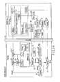
- FIG. 2a description is given of an authentication flow of the memory system having the structure shown in FIG. 1 .
- the host device 20If authentication is started (Start), the host device 20 reads out an encrypted LotID set (SELID: Set of Encrypted LotID) from the NAND flash memory 10 (Step S 11 ).
- SELIDSet of Encrypted LotID
- the host device 20executes, by the selector 21 , a select process for selection from the read-out SELID, and reads out encrypted LotID data which can be decrypted by the host device 20 . Further, the host device 20 obtains LotID by executing, by the decryptor 22 , the above-described decryption process by using the hidden secret information HKey j (Step S 12 ).
- the host device 20generates a random number RN h which is necessary at the time of requesting authentication.
- the random number RN hfor the authentication process, it becomes possible to use, in the subsequent process, a different shared key at each time between the host device 20 and the NAND flash memory 10 (Step S 13 ).
- the host device 20requests authentication (Request authentication) and transmits a pre-stored host constant (HC j ) and the random number RN h to the NAND flash memory 10 (Step S 14 ).
- the NAND flash memory 10receives the request for authentication, loads NKey which is hidden in the hidden area 11 - 2 , and stores the NKey in the data cache 12 (Step S 15 ).
- the NAND flash memory 10generates, by the random number generator 15 , a random number RN c which is necessary for authentication, and sends the random number RN c to the host device (Step S 16 ).
- the NAND flash memory 10uses the loaded NKey and the host constant HC j that has been received in Step S 14 to generate HKey j by the above-described data generation process circuit 13 . Further, the NAND flash memory 10 generates, by the data concatenation process module 14 , concatenated data RN h ⁇ RN c , from the random number RN h received in Step S 14 and the random number RN c generated in Step S 16 .
- the host device 20sends an ID request (Request ID) to the NAND flash memory 10 (Step S 19 ).
- the NAND flash memory 10reads out ChipID and LotID from the ROM area 11 - 3 (Step S 21 ).
- the host device 20calculates, by the exclusive-OR module 29 , an exclusive logical sum between the above-described ID and the LotID obtained in Step S 12 , thereby obtaining ChipID (Step S 24 ).
- HKey jthe set of second key information
- HKey j (+) jis used as an encryption key.
- a cyclic shift operationmay be used.
- the Cyclic shift operationis an operation in which bits are shifted and a bit exceeding digits is carried over to the opposite side.
- a left cyclic shift operationif “11010101” in a binary system is cyclically shifted three times to the left, the result is “10101110”.
- (CyclicLeftShift (HKey j , j)means that HKey j is cyclically shifted to the left by j times.
- the exclusive-OR module 24 shown in FIG. 1is replaced with a left cyclic shift module which executes a left cyclic shift operation.
- the structure of the SELIDis not limited to the above example.
- the host device 20 which stores this HKey jmay be configured such that LotID cannot be decrypted from the encrypted LotID set.
- the encrypted LotID, which can be decrypted by the HKey jis deleted from the SELID.
- the NAND flash memory 10in which a newly configured SELID is recorded, has been used, correct LotID and ChipID cannot be obtained (decrypted) in the host device.
- the host device 20 that is the authenticatormay be provided not only as a dedicated hardware device such as a consumer device, but also as a program (software) which is executable in a PC (personal computer) or the like, and, in some cases, the software functions as a substantial authenticator.
- the NAND flash memory 10 that is the authenticateeis, for instance, recording media or the like. Even in the case where a program called “firmware” mediates in the recording media, an important process or information is stored in a hidden state in hardware in the cell array 11 . Thus, in reality, for example, there is concern that the software, which is executed on the PC, has a lower tamper-resistance (resistance to an attack) than the recording media.
- the first key information (NKey), from which the second key information (HKey) is generatedis hidden in the cell array 11 .
- the second key information (HKey)is hidden in the memory 23 .
- the NAND flash memory 10generates the second key information (HKey) that is same information hidden in the authenticator, by using the source information (HC) that is received from the host device 20 and the first key information (NKey) that is hidden in the NAND flash memory 10 itself.
- the NAND flash memory 10generates the session key (SKey) from the second key information (HKey) and the random number information (RN h , RN C ).
- the host device 20generates the session key (SKey′) from the hidden second key information (HKey) and the random number information (RN h , RN C ). As a result, the NAND flash memory 10 and host device 20 share the session key with the same value.
- the secrecy level of the information, which is hidden in the NAND flash memory (authenticatee) 10 , and the secrecy level of the information, which is hidden in the host device (authenticator) 20can be made asymmetric.
- the secrecy level of the information, which is hidden in the NAND flash memory 10 with a relatively higher tamper-resistancecan be set to be higher than the secrecy level of the information, which is hidden in the host device 20 with a relatively low tamper-resistance.
- the structure of the present embodimentis subject to the environment in which restrictions are imposed on circuit scales, for example, in an environment in which hardware implementation of a public key encryption process or an MKB process, which requires a relatively large circuit scale, is difficult to achieve.
- the key informationis asymmetric, there is no need to use the public key encryption process which requires a relatively large circuit scale.
- the secrecy level of the information hidden in the host device (authenticator) 20 and the secrecy level of the information hidden in the NAND flash memory (authenticatee) 10are made asymmetric. Thereby, use is made of such authentication means that information alone, which is leaked from one device, does not allow disguise as the other device, and the session key (SKey) that is secret information is shared between the authenticator and authenticatee.
- SKeysession key
- circuit scalecan be made relatively small, by implementing the data generation circuit and the encryptor, which constitute the memory system, by the same process, as described above.
- This embodimentrelates to an example in which a plurality of NKeys (first key information) is provided. A detailed description of parts common to those in the first embodiment is omitted.
- index information iis kept in the host device 20 , the index information i indicating which secret information HKey i,j corresponding to secret information NKey i in the NAND flash memory 10 is hidden in the memory 23 .
- the host device 20selects, by the selector 21 , encrypted LotID which can be decrypted by the host device 20 itself, from the SELID by making use of the index information i for designating the secret information, together with the index information j.
- the host device 20transmits the index information i to the NAND flash memory 10 .
- the index information iwhich is necessary for selecting the secret information NKey i hidden in the NAND flash memory 10 , is further transmitted from the host device 20 to the NAND flash memory 10 .
- Step S 18in the NAND flash memory 10 , the index information i is used in order to generate second key information HKey i,j.
- secret information HKeywhich varies depending on the purpose of use, is hidden in the corresponding host device 20 . Therefore, more advantageously, even when HKey or NKey, which was distributed for a specific purpose of use, has been exposed, the other purposes of use are not adversely affected.
- first secret information NKeyis allocated to a video player and second secret information NKey is allocated to an e-book reader
- secret information HKey 1,j /NKey 1which is allocated to the video player, has been exposed
- HKey 1,j /NKey iit is not possible to construct an e-book reader by using the exposed secret information HKey 1,j /NKey i .
- different HKeys/NKeyswere allocated to individual host device makers, even if the secret information has been exposed from a host device of maker A, it is not possible to construct a host device of maker B. Therefore, it becomes possible to newly manufacture and provide such a NAND flash memory 10 that only the host device of the specific maker A, from which the secret information has been exposed, is unable to correctly read out LotID and ChipID.
- This embodimentrelates to an example in which a plurality of NKeys (first key information) is provided for each Lot (e.g. for each NAND maker). A detailed description of parts common to those in the first embodiment is omitted.
- the third embodimentdiffers from the first embodiment.
- SELIDencrypted LotID set
- the index i and SELIDare read out in this order, but the order of read-out is not particularly limited.
- the index information for designating HKeyis composed of two index information pieces, i.e. i and j.
- the SELIDis similar to that in the second embodiment shown in FIG. 6 .
- a plurality of NKeys (first key information) for each Lotis stored in the hidden area 11 - 2 of the NAND flash memory 10 . Further, the index information i for specifying the secret information NKey i is recorded in the ROM area 11 - 3 .
- NAND flash memorieswhich are manufactured by other NAND flash memory makers, can be continuously usable without change, and this is advantageous.
- index information iindex of NKey
- index information imay be stored in user area (normal read/write area) 11 - 1 , instead of the ROM area 11 - 3 .
- the information to be stored in hidden area 11 - 2is high degree of confidentiality, and should not be stored in the other areas.
- the other kind of informationcan be stored in other area such as user area 11 - 1 or ROM area 11 - 3 , for the sake of, for example, data storing step at fabricating of the device or for easy use of data.
- This embodimentrelates to an example in which SELID is recorded in a protected area (Protected area). A detailed description of parts common to those in the first embodiment is omitted.
- the fourth embodimentdiffers from the foregoing embodiments in that the encrypted LotID set (SELID) is recorded in a protected area (Protected area) 11 - 4 of the cell array (Cell array) 11 of the NAND flash memory 10 .
- the protected area (Protected area) 11 - 4is an area in which a data write/read process by access from the outside is permitted only when an authentication process, which is separately implemented in the controller 19 , has been successfully executed.
- This protected area 11 - 4is an area which is provided in, for instance, an SD (registered trademark) card, etc., which are currently marketed.
- the data recorded in the protected area 11 - 4is not only hidden from the outside of the authentic host device 20 which can execute an authentication process with the controller 19 . It is also possible to prevent the user from erroneously rewriting/deleting the data therein.
- the protected area 11 - 4serves also as an area for storing information which is necessary and indispensable for a data reproduction process.
- the SELID relating to this embodimentis transmitted to the host device 20 , after establishing a secure channel 33 through which an authentication process, which is separately provided between the host device 20 and the controller 19 , has been executed.
- Step S 35the host device 20 establishes the secure channel by executing the authentication process which is separately provided between the host device 20 and the controller 19 .
- Step S 35the host device 20 obtains an access permission to the protected area (Protected area) 11 - 4 , and reads out the encrypted LotID set (SELID) via the established secure channel.
- the SELID in the fourth embodimentis the same as the SELID shown in FIG. 3 .
- the encrypted LotID set(SELID) is recorded in the protected area (Protected area) 11 - 4 of the cell array 11 . It is possible, therefore, to prevent such a trouble that the ChipID or LotID cannot be read out due to erroneously rewrite/deletion of the SELID by the user.
- This embodimentrelates to an example in which the random number generator 15 is not provided in the NAND flash memory 10 . A detailed description of parts common to those in the first embodiment is omitted.
- the random number generator (RNG) 15is not provided in the NAND flash memory 10 .
- i-NANDfixed value index information
- the i-NANDis a value which is used when key data SKey j is generated in place of the random number RN c in the first embodiment.
- this valueuse may be made of values generated by various generation means, for instance, a random number value which was generated in advance at the time of manufacture of the NAND flash memory, a hash value of ChipID or LotID, or a value created by encrypting ChipID or LotID by a specific value.
- the NAND flash memory 10further includes a data cache 12 B.
- Step S 16when the NAND flash memory 10 receives an authentication request (Request authentication) from the host device 20 , the NAND flash memory 10 reads out the fixed value index information (i-NAND) from the ROM area 11 - 3 , instead of generating a random number by a random number generator, and sends the fixed value index information (i-NAND) to the host device 20 .
- the NAND flash memory 10reads out the fixed value index information (i-NAND) from the ROM area 11 - 3 , instead of generating a random number by a random number generator, and sends the fixed value index information (i-NAND) to the host device 20 .
- the SELID in the fifth embodimentis the same as the SELID shown in FIG. 3 .
- the above-described random number generator (RNG) 15 in FIG. 1is not included in the NAND flash memory 10 . Therefore, the implementation circuit scale of the NAND flash memory 10 can further be reduced, and microfabrication can advantageously be achieved.
- This embodimentrelates to an example in which verification data (Token) is generated. A detailed description of parts common to those in the first embodiment is omitted.
- the structure example of the sixth embodimentdiffers from the foregoing embodiments in that each of the NAND flash memory 10 and host device 20 generates key data SKey j from secret information HKey j and the concatenated data RN h ⁇ RN c of two random numbers, by using the data generation circuit (Generate) 16 , 26 , and generates verification data (Token) for confirming that the same key data SKey j is generated between the host device and the NAND flash memory.
- the verification datais data which is calculated based on the session key data SKey j and a value shared by the host device 20 and NAND flash memory 10 .
- Generate ( )is described as G ( ).
- the data generation circuitwhich is used for generating the session key SKey j
- the data generation modulewhich is used for generating the Token
- the data generation circuitwhich is used for generating the session key SKey j
- the data generation modulewhich is used for generating the Token
- the purposeis to generate the same data by the host device 20 and NAND flash memory 10 , it is not necessary that the above-described two data generation modules be the same data generation module, and these two data generation modules may be constructed by different modules.
- the generated verification data Tokenis sent from the NAND flash memory to the host device.
- the host device 20determines, by a comparator 35 , whether the received verification data Token and the verification data calculated by the host device itself are identical. If the verification data values Token are identical (Yes), a gate module 36 outputs a session key SKey j to the decryption module (Decrypt) 28 , and continues the subsequent process, as in the first embodiment. On the other hand, if the verification data values Token are different (No), the subsequent process is canceled (Abort).
- the following processis added after the generation of the key data SKey j in the first embodiment.
- Step S 39the host device confirms whether the receive Token corresponds to the Token generated by the host device itself.
- the subsequent processis continuously executed.
- the receive Tokendoes not corresponds to the Token generated by the host device itself, the subsequent authentication process is canceled.
- the SELID in the sixth embodimentis the same as the SELID shown in FIG. 3 .
- the verification data (Token) for confirming that the same key data SKey j is generated between the host device and the NAND flash memoryis generated, and the agreement of the verification data (Token) is determined.
- This embodimentrelates to an example in which another set of IDKeys is used for SELID encryption. A detailed description of parts common to those in the first embodiment is omitted.
- FIG. 15a structure example according to the seventh embodiment is described.
- the structure example of the seventh embodimentdiffers from the foregoing embodiments in that the encryption key, which is used to generate the encrypted LotID set (SELID), is changed to an encryption key IDKey which is different from the HKey that is derived from the NKey.
- the encryption keywhich is used to generate the encrypted LotID set (SELID)
- IDKeywhich is different from the HKey that is derived from the NKey.
- new secret information IDKey kis hidden in the memory 23 , and this IDKey k is used in the decryption process of the SELID that is read out of the NAND flash memory 10 .
- the present embodimentdiffers from the foregoing embodiments. However, there is no change in the decryption process itself.
- the present embodimentdiffers from the foregoing embodiments in that the host device 20 , in Step S 12 , decrypts the encrypted LotID set (SELID), which has been red out of the NAND flash memory 10 , by using the secret information IDKey k and index information k.
- SELIDencrypted LotID set
- the structure example of the SELID in this embodimentis as shown in FIG. 17 .
- the same advantageous effects (1) and (2), as with the above-described first embodiment,can be obtained.
- the LotIDcannot be obtained by decrypting the SELID.
- an authenticatorrelates to an example in which a one-way function is used for calculation at time of ChipID transmission. A detailed description of parts common to those in the first embodiment is omitted.
- the structure example of the eighth embodimentdiffers from the foregoing embodiments in that an encrypted ChipID set (SECID: Set of Encrypted ChipID), which is formed by encrypting not LotIDs but ChipIDs, is recorded in the user area (User area) 11 - 1 in the cell array (Cell array) 11 of the NAND flash memory 10 , and only the ChipID is recorded in the ROM area 11 - 3 .
- SECIDSet of Encrypted ChipID
- the NAND flash memory 10 and host device 20include one-way converters (Oneway) 38 and 39 for executing one-way calculations, instead of encrypting the ID by the session key SKey j .
- the host device 20includes a decryptor 22 , which is similar to the decryptor 22 in the first embodiment, for reading out the SECID from the NAND flash memory 10 , and obtaining the ChipID from the SECID by using the HKey j and index information j.
- the host device 20includes a data verification module 40 for determining a verification result between a value (Oneway(SKey j , ChipID)), which is obtained by oneway-converting the ChipID received from the NAND flash memory 10 , and a oneway conversion value of the ChipID calculated by the host device 20 itself.
- a data verification module 40for determining a verification result between a value (Oneway(SKey j , ChipID)), which is obtained by oneway-converting the ChipID received from the NAND flash memory 10 , and a oneway conversion value of the ChipID calculated by the host device 20 itself.
- the host device 20reads out an encrypted ChipID set (SECID: Set of Encrypted ChipID) from the NAND flash memory 10 (Step S 11 ).
- SECIDSet of Encrypted ChipID
- the host device 20executes the above-described select process for selection from the read-out SECID, and reads out encrypted ChipID data which can be decrypted by the host device 20 . Further, the host device 20 obtains ChipID by executing the above-described decryption process by using the hidden secret information HKey j (Step S 12 ).
- the host device 20generates a random number RN h which is necessary at the time of requesting authentication.
- a different shared keyis used at each time in the subsequent process between the host device 20 and the NAND flash memory 10 (Step S 13 ).
- the host device 20requests authentication (Request authentication) and transmits a pre-stored host constant (HC j ) and the random number RN h to the NAND flash memory 10 (Step S 14 ).
- the NAND flash memory 10generates a random number RN c which is necessary for authentication, and sends the random number RN c to the host device (Step S 15 ).
- the NAND flash memory 10uses the hidden NKey and the HC j that has been received in Step S 14 to generate HKey j by the above-described data generation process. Further, the NAND flash memory 10 generates concatenated data RN h ⁇ RN c , from the random number RN h received in Step S 14 and the random number RN c generated in Step S 15 by the above-described data concatenation process.
- the host device 20sends an ID request (Request ID) to the NAND flash memory 10 (Step S 19 ).
- the NAND flash memory 10reads out ChipID from the ROM area 11 - 3 (Step S 21 ).
- the host device 20executes one-way conversion by using the key data SKey j with which the ChipID has been generated, and finds oneway conversion data Oneway-ID (Step S 39 ).
- the host device 20confirms that the received oneway conversion data Oneway-ID corresponds to the found oneway conversion data Oneway-ID. When both correspond, the host device 20 determines that the above-described ChipID is the correct ChipID. When both do not correspond, the host device 20 determines that the above-described ChipID is an unauthentic ID (Step S 40 ).
- a structure example of the SECID that is the encrypted ChipID setis, similarly, as shown in FIG. 20 .
- the encrypted ChipID set(SECID), which is formed by encrypting not LotIDs but ChipIDs, is recorded in the user area (User area) 11 - 1 in the cell array (Cell array) 11 of the NAND flash memory 10 , and only the ChipID is recorded in the ROM area 11 - 3 .
- the amount of ID information, which has to be stored in the NAND flash memory 10can be reduced.
- the present embodimentincludes both the changes added to the first embodiment in the seventh embodiment and eighth embodiment.
- the ninth embodimentis different from the first embodiment, mainly in that the IDKey is introduced and the SELID is changed to the SECID.
- FIG. 22illustrates an authentication flow relating to the ninth embodiment.
- the authentication flow of the ninth embodimentis the combination of the authentication flow of the seventh embodiment and that of the eighth embodiment.
- a structure example of the SECID that is the encrypted ChipID setis, similarly, as shown in FIG. 23 .
- the present embodimentincludes the different points which are added in the third, seventh and eighth embodiments.
- the tenth embodimentis different from the first embodiment, mainly in that the IDKey is introduced, the SELID is changed to the SECID, and plural secret information pieces HKeys are hidden in the host device.
- the authentication flowis different from that of the ninth embodiment in that an authentication flow, which is described below, is added.
- the host device 20requests authentication (Request authentication) in Step S 14 .
- process flow illustrated in FIG. 25is merely an example.
- the process flowis not limited to this example, if necessary data can be obtained in advance in processes such as the read-out of the index information i and the select process of HKey i,j.
- a structure example of the SECID that is the encrypted ChipID setis, similarly, as shown in FIG. 23 .
- the same advantageous effects (1) and (2), as with the above-described first embodiment,can be obtained.
- an authenticatorrelates to an example in which the random number generator 15 is not provided in the NAND flash memory 10 in the tenth embodiment. A detailed description of parts common to those in the first embodiment is omitted.
- the present embodimentdiffers from the tenth embodiment in that the random number generator (RNG) 15 , which is provided in the NAND flash memory in the tenth embodiment, is not provided.
- RNGrandom number generator
- the session key data SKey i,jis generated from the concatenated data of two random numbers RN h and RN c and the secret data HKey i,j .
- the session key data SKey i,jis generated from the random number RN h and the secret data HKey i,j.
- the present embodimentillustrates a method of reading out identification information ChipID, which is recorded in the NAND flash memory that is the authenticatee, in the state in which the identification information ChipID is hidden from a third party, and surely confirming the data that is read out from the authenticatee, and shows a structure example in the case where this method is applied to the NAND flash memory.
- the NAND flash memory 10is an authenticatee, as described above.
- the NAND flash memory 10includes a cell array 11 , data caches 12 A and 12 B which are disposed in a peripheral area of the cell array 11 , data generation modules (Generate) 13 and 16 , and a one-way converter (Oneway) 38 .
- the cell array (Cell array) 11includes a ROM area (ROM area) 11 - 3 , a hidden area (Hidden area) 11 - 2 and a user area (User area) 11 - 1 .
- the ROM area (ROM area) 11 - 3is an area in which data record from the outside is prohibited and data read from the outside is permitted.
- a ChipIDwhich is identification information
- index information iindex of NKey
- the ChipID and index iare recorded, in general, in the state in which the ChipID and index i are error-correction-encoded, so that the correct identification information may be read out even when an error has occurred in the data.
- the error-correction encoding/decodingis not particularly illustrated.
- the hidden area (Hidden area) 11 - 2is an area in which the outside of the NAND flash memory 10 is prohibited from data record, and in which data read is prohibited (Read/Program inhibit).
- NKey iwhich is secret information that is used by the NAND flash memory 10 in the authentication, is recorded.
- the ChipIDmay be recorded in the hidden area, in place of the ROM area.
- the user area (User area) 11 - 1is an area in which data record and data read can be freely executed.
- SECIDSet of Encrypted ChipID
- content datasuch as photos, video, music or e-books, are recorded in the user area 11 - 1 .
- the structure example of the SECID that is the encrypted ChipIDis the same as shown in FIG. 23 .
- the data cache (Data cache) 12 A, 12 Btemporarily stores data which has been read out from the cell array 11 .
- Each of the data generation modules (Generate) 13 , 16is a module which outputs new data from a plurality of input information pieces. In order to reduce the whole module scale, it is possible to construct the data generation modules (Generate) 13 , 16 by the same module as the above-described oneway converter or a module which makes applicable use of the one-way converter. Similarly, the two data generation modules, which are depicted as different structural elements in order to make the data processing procedure easy to understand, may be realized by repeatedly utilizing the same module.
- Each of the data generation modules (Generate) 13 , 16is a module which generates output data by a predetermined calculation from a plurality of input data.
- the data generation modulesare used in order to convert information (HC j ), which has been received from the host device 20 , by using the above-described secret information NKey i , thereby generating HKey i,j , and to convert, by using the HKey j , the random number RN h which has been received from the host device 20 , thereby generating a session key SKey i,j .
- AESAdvanced Encryption Standard
- encryptorsmay be used for the data generation modules 13 and 16 .
- the oneway converter (Oneway) 38is a module which executes oneway conversion of the input data and the key data which is separately input, and outputs oneway-converted input data.
- the identification information ChipIDis recorded in the hidden area in place of the ROM area
- the identification information ChipIDwhich is the input data of the oneway converter, is read out from the hidden area.
- the oneway converter 38may also be used as the data generation circuit.
- an output module for outputting datawhich is to be sent to the host device 20 via the controller 19 , may actually be disposed as a structural element.
- the host device (Host) 20includes a random number generator (RNG) 25 , an exclusive-OR module (EXOR) 24 , data selectors (Select) 21 - 1 and 21 - 2 , a decryptor (Decrypt) 22 , a data generator (Generate) 27 , a one-way converter (Oneway) 39 , and a data verification module (Verify) 40 .
- RNGrandom number generator
- EXORexclusive-OR
- Data selectorsSelect
- Decryptdecryptor
- Decryptdecryptor
- Generatedata generator
- Onewayone-way converter
- Verifydata verification module
- an error correction process modulefor instance, which is not shown, may be included as a structural element, where necessary.
- the random number generator (RNG) 25generates RN h which is used for authentication.
- the exclusive-OR module (EXOR) 24calculates an exclusive logical sum of two input data, and outputs the calculation result.
- the first-stage data selector (Select 1 ) 21 - 1selects, by using index information k of secret information HKey j , encrypted ChipID data which can be decrypted by using secret information IDKey k that is hidden in the host device, from the encrypted ChipID set (SECID) which has been read out of the NAND flash memory 10 .
- the secret information IDKey k and HKey i,jare recorded in an internal dedicated memory after being encrypted by a unique method of the maker.
- the secret information IDKey k and HKey i,jare stored in the state in which the secret information IDKey k and HKey i,j can be protected against unlawful analysis by a tamper-resistant software (TRS) technology.
- TRStamper-resistant software
- the secret information IDKey k and HKey i,jare stored, after taking such a measure as hiding the secret information IDKey k and HKey i,j by using the function of the security module.
- the decryptor (Decrypt) 22decrypts input data by key data which is separately input, and outputs decrypted input data.
- the decryptor 22is used in order to obtain ChipID by decrypting encrypted ChipID data which has been selected by the first data selector, by using, as key information, a calculation result by the exclusive-OR module with respect to the secret information IDKey k hidden in the host device and index information k for identifying the secret information IDKey k , where necessary.
- the data generator (Generate) 27is an arithmetic module which generates output data by a predetermined calculation from a plurality of input data.
- the data generator 27is used in order to convert, by using the secret information HKey i,j hidden in the host device, the random number RN h , which has been generated by the host device 20 itself, thereby generating a session key SKey i,j .
- the data generator 27can use, for example, an AES encryption calculation.
- the oneway converter (Oneway) 39converts, by a oneway function, the ChipID which has been output from the decryptor, by using the SKey i,j which has been output from the data generator, thereby generating oneway conversion identification information Oneway-ID.
- the data verification module (Verify) 40compares the oneway conversion identification information Oneway-ID, which has been received from the NAND flash memory 10 , and the oneway conversion identification information obtained from the oneway converter in the host device. When both information values correspond, the data verification module (Verify) 40 determines that the above-described ChipID obtained by the decryptor is the correct ChipID. When both information values do not correspond, the data verification module (Verify) 40 determines that the above-described ChipID is an unauthentic ID.
- An error correction process module, etc., which are not shown,may be provided as structural elements, where necessary.
- the host device 20reads out an encrypted ChipID set (SECID: Set of Encrypted ChipID) from the NAND flash memory 10 (Step S 11 ).
- SECIDSet of Encrypted ChipID
- the host device 20executes, by the data selector (Select 1 ) 21 - 1 , a data select process for selection from the read-out SECID, and reads out encrypted ChipID data which can be decrypted by the host device 20 . Further, the host device 20 obtains ChipID by executing, by the decryptor 22 , the decryption process by using the hidden secret information IDKey k (Step S 12 ).
- the host device 20generates a random number RN h which is necessary at the time of requesting authentication (Step S 13 ).
- RN ha random number which is necessary at the time of requesting authentication
- the host device 20requests authentication (Request authentication) and transmits a pre-stored host constant (HC j ) and the random number RN h to the NAND flash memory 10 (Step S 14 ).
- the host device 20sends an ID request (Request ID) to the NAND flash memory 10 (Step S 19 ).
- the NAND flash memory 10reads out ChipID from the ROM area (Step S 21 ).
- the host device 20executes a one-way conversion process in the oneway converter 39 by using the key data SKey i,j with which the ChipID has been generated, and finds oneway conversion data Oneway-ID (Step S 39 ).
- the host device 20confirms that the received oneway conversion data Oneway-ID corresponds to the found oneway conversion data. When both correspond, the host device 20 determines that the above-described ChipID is the correct ChipID. When both do not correspond, the host device 20 determines that the above-described ChipID is an unauthentic ID (Step S 40 ).
- the eleventh embodimentthere is no need to provide the random number generator 15 in the NAND flash memory 10 . Therefore, the advantageous effects of the first embodiment and the advantageous effects, which are added in the tenth embodiment, can similarly be obtained, and the implementation circuit scale of the NAND flash memory can, advantageously, further be reduced.
- This embodimentrelates to an example in which index information ID-index, which is necessary for specifying ChipID, is written. A detailed description of parts common to those in the first embodiment is omitted.
- FIG. 28a structure example according to the twelfth embodiment is described.
- the present embodimentdiffers from the eleventh embodiment in that index information ID-index, which is necessary for specifying ChipID, is written in the ROM area 11 - 3 of the NAND flash memory 10 , the ChipID is recorded in the hidden area (Hidden area) 11 - 3 , and a data cache (Data cache) 12 C, for instance, for reading out the ChipID is included, where necessary.
- index information ID-indexwhich is necessary for specifying ChipID
- a structure example of the SECID that is the encrypted ChipIDis similar to that shown in FIG. 23 .
- the NAND flash memory 10reads out the ChipID via the data cache, where necessary.
- the process flowis substantially the same as that in the eleventh embodiment.
- This write processis not particularly necessary, for example, when the encrypted ChipID set (SECID) is written at the time of manufacture of the NAND flash memory 10 .
- the SECID write processis necessary, for example, in the case where the NAND flash memory 10 and controller 19 are combined and are obtained by general users as a storage media product such as an SD (registered trademark) card, and the SECID is written later in the market at the time of use of the card.
- SDregistered trademark
- FIG. 29shows the case in which data is recorded in a storage medium in the state in which the SECID has not yet been recorded, as described above.
- secret information NKey i and identification information ChipIDare recorded in the hidden area 11 - 2 , index information i which is necessary for specifying the secret information NKey i and index information ID-index which is necessary for specifying the identification information ChipID are written in the ROM area 11 - 3 .
- the SECIDhas not yet been written in the NAND flash memory 10 .
- a data cache 12is disposed, where necessary, in the NAND flash memory 10 .
- ChipID generatorGenerate ChipID
- EncryptEncryptor
- ID-indexis expressed as follows:
- ID-indexEncrypt (K m , ChipID).
- the ID-indexis transmitted to the server 60 via the Internet 50 .
- the generator 62decrypts the received ID-index by using the conversion key K m , thereby obtaining ChipID.
- the ChipIDis expressed as follows:
- ChipIDDecrypt (K m , ID-index).
- the conversion key K mmay be made common to all makers of NAND flash memories 10 . However, the conversion key K m may also be made different between the makers of NAND flash memories 10 .
- the host device 20has a function of determining whether new write of SECID is necessary or not, and requesting SECID from the server where necessary.
- the SECID write processis started (Start), and the host device 20 issues a SECID request to the server 60 (Step S 55 ).
- the server 60requests, from the NAND flash memory 10 , the index information ID-index which is necessary for specifying the ChipID (Step S 60 ).
- the NAND flash memory 10reads out the ID-index from the ROM area 11 - 3 , and sends the ID-index to the server (Step S 61 ).
- the server 60generates ChipID by the ChipID generator 62 , by using the received ID-index (Step S 62 ).
- the server 60sends the generated encrypted ChipID set (SECID) to the NAND flash memory (Step S 64 ).
- the NAND flash memory 10writes and records the received encrypted ChipID set (SECID) in the user area 11 - 1 (Step S 65 ).
- the 13th embodimentrelates to an example of the NAND flash memory 10 , controller 19 and host device 20 , which are applicable to the above-described embodiments.
- an SD cardregistered trademark
- a memory cardis taken as an example of a memory card.
- FIG. 32in this embodiment, functional blocks of the host device, which is connected to the memory card, are illustrated.
- the respective functional blockscan be realized by either hardware or computer software, or by a combination of both.
- the respective blocksare described, in general, from the standpoint of their functions, so as to clarify by which of them each block is realized. Whether such functions are executed as hardware or software depends on concrete modes of implementation or on design restrictions imposed on the entire system. A person skilled in the art may realize these functions by various methods in each concrete mode of implementation, but all methods of implementation fall within the scope of the present invention.
- the host device 20includes software 211 such as an application or an operating system.
- the software 211is instructed by the user to write data in the memory card, or to read out data from the memory card.
- the software 211instructs a file system 212 to write and read data.
- the file system 212is a scheme for managing file data which is recorded in a storage medium that is an object of management.
- the file system 212records management information in a memory area in the storage medium, and manages the file data by using the management information.
- the host device 20includes an SD interface 213 .
- the SD interface 213is composed of hardware and software, which are necessary for executing an interface process between the host device 20 and the memory card.
- the host device 20communicates with the memory card via the SD interface 213 .
- the SD interface 213specifies various protocols which are necessary for communication between the host device 20 and the memory card, and includes a set of various commands which are mutually recognizable by an SD interface 131 of the memory card, which will be described later.
- the SD interface 213includes a hardware structure (arrangement of pins, number of pins, etc.) which is connectable to the SD interface 131 of the memory card.
- the memory cardincludes a NAND flash memory 10 and a controller 19 for controlling the memory 10 .
- the memory cardWhen the memory card is connected to the host 20 , or when the host 20 is turned on in the state in which the memory card is inserted in the host 20 that is in the OFF state, the memory card is supplied with power, executes an initializing process, and executes a process corresponding to the access from the host 20 .
- the NAND memory 10stores data in a nonvolatile state, and executes data write and read in a unit called “page” which comprises a plurality of memory cells. A unique physical address is allocated to each page. In addition, the memory 10 executes erase of data in a unit called “block” (erase block) which comprises a plurality of pages. In some cases, a physical address is allocated to a physical block unit.
- the controller 19manages the storage state of data by the memory 10 .
- the management of the storage stateincludes managing a relationship between a physical address of a page (or a physical block) and a logical address of data which is stored in this page, and managing which physical address is indicative of a page (or a physical block) that is in an erase state (a state in which no data is written or invalid data is stored).
- the controller 19includes an SD interface 131 , an MPU 132 , a ROM (read only memory) 133 , a RAM (random access memory) 134 , and a NAND interface 135 .
- the SD interface 131is composed of hardware and software, which are necessary for executing an interface process between the host 20 and the controller 19 . Like the SD interface 213 , the SD interface 131 specifies protocols which enable communication between both, includes a set of various commands, and also includes a hardware structure (arrangement of pins, number of pins, etc.).
- the memory card (controller 19 )communicates with the host 20 via the SD interface 131 .
- the SD interface 131includes a register 136 .
- the MPU 132controls the entire operation of the memory card. For example, when the memory card is supplied with power, the MPU 132 reads out firmware (control program), which is stored in the ROM 133 , into the RAM 134 , and executes a predetermined process. The MPU 132 creates various tables on the RAM 134 according to the control program, or executes a predetermined process on the memory 10 according to a command which is received from the host 20 .
- firmwarecontrol program
- the ROM 133stores, e.g. a control program which is controlled by the MPU 132 .
- the RAM 134is used as a working area of the MPU 132 , and temporarily stores the control program or various tables. Such tables include a conversion table (logical/physical table) for converting a logical address allocated to data by the file system 212 to a physical address of a page in which the data is actually stored.
- the NAND interface 135executes an interface process between the controller 19 and the memory 10 .
- the memory areas in the NAND flash memory 10include, for example, a user area (User area), a hidden area (Hidden area), a protected area (Protected area) and a ROM area (ROM area), as described above, in accordance with the kinds of data which is stored.
- the controller 19secures a part of the user data area, and stores control data (e.g. logical/physical table) which is necessary for the operation of the controller 19 itself.
- FIG. 33shows a concrete entire structure example of the NAND flash memory 10 .
- the NAND flash memory 10 of this embodimentincludes a memory cell array 11 , a control circuit 19 , an authentication circuit 151 , a bit line control circuit 152 , a column decoder 153 , a data input/output buffer 154 , a data input/output terminal 155 , a word line driving circuit 156 , a control signal input terminal 158 , and a power generation circuit 159 .
- the memory cell array 11is composed of a plurality of blocks (BLOCK 1 to BLOCK n). Each of the blocks (BLOCK 1 to BLOCK n) includes a plurality of memory cells which are arranged at intersections between word lines and bit lines.
- BLOCK 1is the above-described ROM area 11 - 3 .
- BLOCK 2is the hidden area 11 - 2 .
- the other blocksare, for example, user areas (User area) 11 - 1 , which are accessible from the host device 20 .
- the ROM area 11 - 3is, for example, an OTP (One Time Program) block, and only one-time write is permitted. After data write, a block decoder is controlled by using means such as an electric fuse, a laser fuse or a ROM fuse, thereby prohibiting an erase operation.
- the hidden area 11 - 2is set in such a state that the hidden area 11 - 2 cannot be selected by, for example, decoding with an external address.
- the hidden area 11 - 2is an area from which data can be read out by only the control circuit 19 in the NAND flash memory.
- the authentication circuit 151includes, for example, the above-described data cache 12 , generation circuits 13 and 16 , concatenation circuit 14 , random number generator 15 , exclusive-OR circuit 17 , and encryptor 18 .
- the authentication circuit 151is controlled by the control circuit 19 .
- the bit line control circuit 152reads out data of a memory cell in the memory cell array 11 via a bit line, and detects the state of a memory cell in the memory cell array 11 via a bit line. In addition, the bit line control circuit 152 applies a write control voltage to a memory cell in the memory cell array 11 via a bit line, thereby writing data in the memory cell.
- bit line control circuit 152a data memory circuit, such as a page buffer (not shown), is provided, and this data memory circuit is selected by the column decoder 153 .
- the data of the memory cell, which has been read out to the data memory circuit,is output to the outside from the data input/output terminal 155 via the data input/output buffer 154 .
- the data input/output terminal 155is connected to, for example, an external host device 20 .
- the data input/output terminal 155has a bus width of, e.g. 8 bits or 16 bits.
- the NAND flash memory 10may support a high-speed interface standard such as a toggle mode interface. In the toggle mode interface, for example, data transfer is performed via the data input/output terminal 155 , in sync with both the rising and falling edges of a data strobe signal (DQS).
- DQSdata strobe signal
- the host device 20is, for example, a microcomputer, and receives data which is output from the data input/output terminal 155 .
- the host device 20outputs various commands CMD (write command, read command, erase command, status read command, etc.) for controlling the operation of the NAND flash memory 10 , addresses ADD, and data DT.
- the write data DTwhich has been input to the data input/output terminal 155 from the host device 20 , is supplied via the data input/output buffer 154 to the data memory circuit (not shown) which is selected by the column decoder 153 .
- the commands CMD and addresses ADDare supplied to the control circuit 19 .
- the word line driving circuit 156under the control of the control circuit 19 , selects a word line in the memory cell array 11 , and applies to the selected word line the voltage that is necessary for data read, write or erase.
- the voltage generation circuit 159under the control of the control circuit 19 , supplies necessary voltages for the operations of the connected structural circuits shown in the Figure. For example, the voltage generation circuit 159 boosts an external voltage which is supplied from the host device, and generates a voltage which is applied to the word line at a time of data read, write or erase.
- the control circuit (Controller) 19delivers necessary control signals and control voltages to the respective connected circuits, thereby to control the operation of the entirety of the NAND flash memory 10 .
- the control circuit 19is connected to the memory cell array 11 , authentication circuit 151 , bit line control circuit 152 , column decoder 153 , data input/output buffer 154 , word line driving circuit 156 and voltage generation circuit 159 .
- the connected structural circuitsare controlled by the control circuit 19 .
- the control circuit 19is connected to the control signal input terminal 158 , and is controlled by a combination of control signals, such as a WE (write enable) signal, a RE (read enable) signal, an ALE (address latch enable) signal and a CLE (command latch enable) signal, which are input via the control signal input terminal 158 from the host device 20 .
- control signalssuch as a WE (write enable) signal, a RE (read enable) signal, an ALE (address latch enable) signal and a CLE (command latch enable) signal, which are input via the control signal input terminal 158 from the host device 20 .
- the word line driving circuit 156 , bit line control circuit 152 , column decoder 153 and control circuit 19constitute a data write circuit, a data read circuit and a data erase circuit.
- the host device 20detects whether the NAND flash memory 10 is executing an internal operation, such as a write operation, a read operation or an erase operation, by monitoring an RY/BY (ready/busy) signal output terminal (not shown).
- the control circuit 19outputs an RY/BY signal via the RY/BY signal output terminal.
- FIG. 34a structure example of the block (BLOCK), which constitutes the memory cell array, is described.
- the block BLOCK 1 in FIG. 33is described by way of example.
- this blockis a data erase unit.
- the block BLOCK 1comprises a plurality of memory cell units MU which are arranged in a word line direction (WL direction).
- the memory cell unit MUcomprises a NAND string (memory cell string) which is arranged in a bit line direction (BL direction) crossing the WL direction and is composed of 8 memory cells MC 0 to MC 7 having current paths connected in series; a source-side select transistor S 1 connected to one end of the current path of the NAND string; and a drain-side select transistor S 2 connected to the other end of the current path of the NAND string.
- the memory cell unit MUcomprises 8 memory cells MC 0 to MC 7 .
- the number of memory cellsis not limited to 8, and may be two or more, for example, 56 or 32.
- the other end of the current path of the source-side select transistor S 1is connected to a source line SL.
- the other end of the current path of the drain-side select transistor S 2is connected to a bit line BLm ⁇ 1 which is provided on an upper side of the memory cell unit MU in association with each memory cell unit MU and extends in the BL direction.
- Word lines WL 0 to WL 7extend in the WL direction, and are connected commonly to the control electrodes of the plural memory cells in the WL direction.
- a select gate line SGSextends in the WL direction, and is connected commonly to the plural select transistors S 1 in the WL direction.
- a select gate line SGDextends in the WL direction, and is connected commonly to the plural select transistors S 2 in the WL direction.
- a page (PAGE)is present in association with each of the word lines WL 0 to WL 7 .
- a page 7(PAGE 7) is present in association with the word line WL 7 . Since a data read operation and a data write operation are executed in units of the page (PAGE), the page (PAGE) is a data read unit and a data write unit.
Landscapes
- Engineering & Computer Science (AREA)
- Computer Security & Cryptography (AREA)
- Theoretical Computer Science (AREA)
- Signal Processing (AREA)
- Computer Networks & Wireless Communication (AREA)
- Computer Hardware Design (AREA)
- Software Systems (AREA)
- Physics & Mathematics (AREA)
- General Engineering & Computer Science (AREA)
- General Physics & Mathematics (AREA)
- Databases & Information Systems (AREA)
- Health & Medical Sciences (AREA)
- Bioethics (AREA)
- General Health & Medical Sciences (AREA)
- Storage Device Security (AREA)
Abstract
Description
Claims (2)
Priority Applications (4)
| Application Number | Priority Date | Filing Date | Title |
|---|---|---|---|
| US14/090,740US9225513B2 (en) | 2011-08-31 | 2013-11-26 | Authenticator, authenticatee and authentication method |
| US14/939,426US9887841B2 (en) | 2011-08-31 | 2015-11-12 | Authenticator, authenticatee and authentication method |
| US15/827,867US10361850B2 (en) | 2011-08-31 | 2017-11-30 | Authenticator, authenticatee and authentication method |
| US15/936,881US10361851B2 (en) | 2011-08-31 | 2018-03-27 | Authenticator, authenticatee and authentication method |
Applications Claiming Priority (3)
| Application Number | Priority Date | Filing Date | Title |
|---|---|---|---|
| JP2011-189979 | 2011-08-31 | ||
| JP2011189979AJP5214782B2 (en) | 2011-08-31 | 2011-08-31 | Memory device, storage medium, host device, and system |
| PCT/JP2012/058276WO2013031270A1 (en) | 2011-08-31 | 2012-03-19 | Authenticator, authenticatee and authentication method |
Related Parent Applications (1)
| Application Number | Title | Priority Date | Filing Date |
|---|---|---|---|
| PCT/JP2012/058276ContinuationWO2013031270A1 (en) | 2011-08-31 | 2012-03-19 | Authenticator, authenticatee and authentication method |
Related Child Applications (1)
| Application Number | Title | Priority Date | Filing Date |
|---|---|---|---|
| US14/090,740ContinuationUS9225513B2 (en) | 2011-08-31 | 2013-11-26 | Authenticator, authenticatee and authentication method |
Publications (2)
| Publication Number | Publication Date |
|---|---|
| US20130054961A1 US20130054961A1 (en) | 2013-02-28 |
| US8661527B2true US8661527B2 (en) | 2014-02-25 |
Family
ID=47745403
Family Applications (5)
| Application Number | Title | Priority Date | Filing Date |
|---|---|---|---|
| US13/486,684ActiveUS8661527B2 (en) | 2011-08-31 | 2012-06-01 | Authenticator, authenticatee and authentication method |
| US14/090,740Expired - Fee RelatedUS9225513B2 (en) | 2011-08-31 | 2013-11-26 | Authenticator, authenticatee and authentication method |
| US14/939,426ActiveUS9887841B2 (en) | 2011-08-31 | 2015-11-12 | Authenticator, authenticatee and authentication method |
| US15/827,867Expired - Fee RelatedUS10361850B2 (en) | 2011-08-31 | 2017-11-30 | Authenticator, authenticatee and authentication method |
| US15/936,881Expired - Fee RelatedUS10361851B2 (en) | 2011-08-31 | 2018-03-27 | Authenticator, authenticatee and authentication method |
Family Applications After (4)
| Application Number | Title | Priority Date | Filing Date |
|---|---|---|---|
| US14/090,740Expired - Fee RelatedUS9225513B2 (en) | 2011-08-31 | 2013-11-26 | Authenticator, authenticatee and authentication method |
| US14/939,426ActiveUS9887841B2 (en) | 2011-08-31 | 2015-11-12 | Authenticator, authenticatee and authentication method |
| US15/827,867Expired - Fee RelatedUS10361850B2 (en) | 2011-08-31 | 2017-11-30 | Authenticator, authenticatee and authentication method |
| US15/936,881Expired - Fee RelatedUS10361851B2 (en) | 2011-08-31 | 2018-03-27 | Authenticator, authenticatee and authentication method |
Country Status (1)
| Country | Link |
|---|---|
| US (5) | US8661527B2 (en) |
Cited By (4)
| Publication number | Priority date | Publication date | Assignee | Title |
|---|---|---|---|---|
| US20140089675A1 (en)* | 2011-08-31 | 2014-03-27 | Kabushiki Kaisha Toshiba | Authenticator, authenticatee and authentication method |
| US20180165438A1 (en)* | 2016-12-12 | 2018-06-14 | Fanuc Corporation | Operator identification system |
| CN108875413A (en)* | 2017-05-12 | 2018-11-23 | 晨星半导体股份有限公司 | Functional circuit enabling method and chip using same |
| US20250106203A1 (en)* | 2014-04-09 | 2025-03-27 | Cardex Systems Inc. | Self-authenticating chips |
Families Citing this family (25)
| Publication number | Priority date | Publication date | Assignee | Title |
|---|---|---|---|---|
| JP2012084071A (en) | 2010-10-14 | 2012-04-26 | Toshiba Corp | Digital content protection method, decryption method, reproducing device, memory medium and cryptographic device |
| JP5275432B2 (en) | 2011-11-11 | 2013-08-28 | 株式会社東芝 | Storage medium, host device, memory device, and system |
| JP5100884B1 (en) | 2011-12-02 | 2012-12-19 | 株式会社東芝 | Memory device |
| JP5112555B1 (en) | 2011-12-02 | 2013-01-09 | 株式会社東芝 | Memory card, storage media, and controller |
| JP5204290B1 (en) | 2011-12-02 | 2013-06-05 | 株式会社東芝 | Host device, system, and device |
| JP5204291B1 (en) | 2011-12-02 | 2013-06-05 | 株式会社東芝 | Host device, device, system |
| JP5275482B2 (en) | 2012-01-16 | 2013-08-28 | 株式会社東芝 | Storage medium, host device, memory device, and system |
| US8762717B2 (en)* | 2012-06-15 | 2014-06-24 | Kabushiki Kaisha Toshiba | Authentication device |
| US9201811B2 (en) | 2013-02-14 | 2015-12-01 | Kabushiki Kaisha Toshiba | Device and authentication method therefor |
| US8984294B2 (en) | 2013-02-15 | 2015-03-17 | Kabushiki Kaisha Toshiba | System of authenticating an individual memory device via reading data including prohibited data and readable data |
| US9722774B2 (en)* | 2015-04-29 | 2017-08-01 | Samsung Electronics Co., Ltd. | Non-leaky helper data: extracting unique cryptographic key from noisy F-PUF fingerprint |
| US10163282B2 (en)* | 2016-03-30 | 2018-12-25 | Intermec, Inc. | Systems and methods for authentication |
| WO2017176951A1 (en)* | 2016-04-05 | 2017-10-12 | Tfor Llc | A transencrypting method and apparatus for removing information from data transmitted over networks and stored in data storage facilities |
| CN107493166A (en)* | 2016-06-13 | 2017-12-19 | 阿里巴巴集团控股有限公司 | The storage and read method of a kind of private key, device and server |
| US10484350B2 (en)* | 2017-04-26 | 2019-11-19 | At&T Intellectual Property I, L.P. | Privacy-preserving location corroborations |
| EP3439229A1 (en)* | 2017-08-02 | 2019-02-06 | Siemens Aktiengesellschaft | Method and devices for achieving a safety function, particularly in the vicinity of a device control and/or system control |
| US11275920B1 (en) | 2017-09-27 | 2022-03-15 | Apple Inc. | Elongated fingerprint sensor |
| CN107819579B (en)* | 2017-12-13 | 2021-08-24 | 西安Tcl软件开发有限公司 | A user request processing method, server and computer-readable storage medium |
| JP2019133345A (en) | 2018-01-30 | 2019-08-08 | 東芝メモリ株式会社 | Data accumulating device, data processing system and data processing method |
| CN108376211B (en)* | 2018-02-07 | 2020-10-20 | 杭州矩视科技有限公司 | Software authorization management method, server and system |
| US10256974B1 (en)* | 2018-04-25 | 2019-04-09 | Blockchain Asics Llc | Cryptographic ASIC for key hierarchy enforcement |
| CN108600256A (en)* | 2018-05-08 | 2018-09-28 | 山东浪潮通软信息科技有限公司 | A kind of Information Exchange System and method |
| US11189248B1 (en) | 2020-05-06 | 2021-11-30 | Apple Inc. | Systems and methods for switching vision correction graphical outputs on a display of an electronic device |
| US12093359B2 (en) | 2020-09-25 | 2024-09-17 | Apple Inc. | Electronic device having a sealed biometric input system |
| US11783629B2 (en) | 2021-03-02 | 2023-10-10 | Apple Inc. | Handheld electronic device |
Citations (83)
| Publication number | Priority date | Publication date | Assignee | Title |
|---|---|---|---|---|
| US4757468A (en) | 1982-09-22 | 1988-07-12 | Intel Corporation | Authenticated read-only memory |
| JPH03171231A (en) | 1989-11-30 | 1991-07-24 | Toshiba Corp | microcomputer system |
| JPH08204702A (en) | 1995-01-30 | 1996-08-09 | Nec Corp | Cipher key management equipment |
| JPH10232918A (en) | 1997-02-19 | 1998-09-02 | Canon Inc | Image file, image processing apparatus for processing the same, image processing method, and image processing system |
| JP2000122931A (en) | 1998-10-15 | 2000-04-28 | Toshiba Corp | Digital integrated circuit |
| WO2001011883A1 (en) | 1999-08-10 | 2001-02-15 | Intel Corporation | System and method for securely distributing content to groups of receivers |
| JP2001209305A (en) | 2000-01-25 | 2001-08-03 | Sony Corp | Data processing system, recording device, data processing method and program providing medium |
| EP1126355A1 (en) | 2000-02-14 | 2001-08-22 | Kabushiki Kaisha Toshiba | Method and system for distributing programs using tamper resistant processor |
| WO2002033521A2 (en) | 2000-10-17 | 2002-04-25 | Telefonaktiebolaget L M Ericsson (Publ) | Method and apparatus for controlling access to functions with different security levels |
| US20020087814A1 (en) | 2000-12-28 | 2002-07-04 | Ripley Michael S. | Verifying the integrity of a media key block by storing validation data in the cutting area of media |
| US20020116632A1 (en) | 2001-02-22 | 2002-08-22 | Hitachi, Ltd. | Tamper-resistant computer system |
| US20030070082A1 (en)* | 2001-10-10 | 2003-04-10 | Hideki Nimura | Method and apparatus for recording information including secret information and method and apparatus for reproduction thereof |
| US20030105961A1 (en) | 2001-11-30 | 2003-06-05 | Peter Zatloukal | Avoiding attachment of an ineligible smart interchangeable cover to an electronic device |
| US20030154355A1 (en) | 2002-01-24 | 2003-08-14 | Xtec, Incorporated | Methods and apparatus for providing a memory challenge and response |
| JP2003233795A (en) | 1999-04-27 | 2003-08-22 | Matsushita Electric Ind Co Ltd | Semiconductor memory card and reading device |
| JP2004030326A (en) | 2002-06-26 | 2004-01-29 | Sony Corp | Contents use managing system, information processor or information processing method for using or providing contents and computer program |
| US20040039924A1 (en) | 2001-04-09 | 2004-02-26 | Baldwin Robert W. | System and method for security of computing devices |
| US6829676B2 (en) | 1999-10-21 | 2004-12-07 | Matsushita Electric Industrial Co., Ltd. | Semiconductor memory card access apparatus, a computer-readable recording medium, an initialization method, and a semiconductor memory card |
| US20050182948A1 (en) | 2004-02-17 | 2005-08-18 | Vixs Systems Inc. | Method and system for secure content distribution |
| US6950379B2 (en) | 2003-03-28 | 2005-09-27 | Mediatek Inc. | Burst cutting area extraction method and device |
| JP2005316946A (en) | 2004-03-31 | 2005-11-10 | Seiko Epson Corp | Layout rule generation system, layout system, layout rule generation program, layout program and storage medium, layout rule generation method and layout method |
| US20050257243A1 (en) | 2004-04-27 | 2005-11-17 | Microsoft Corporation | Method and system for enforcing a security policy via a security virtual machine |
| JP2005341156A (en) | 2004-05-26 | 2005-12-08 | Toshiba Corp | Storage medium conversion method, program and device |
| US20060060065A1 (en)* | 2004-09-17 | 2006-03-23 | Sony Corporation | Information processing apparatus and method, recording medium, program, and information processing system |
| US20060085644A1 (en)* | 2004-10-15 | 2006-04-20 | Kabushiki Kaisha Toshiba | Information processing apparatus and information processing method |
| US7065648B1 (en) | 1999-06-16 | 2006-06-20 | Kabushiki Kaisha Toshiba | Mutual authentication method, recording apparatus, reproducing apparatus, and recording medium |
| JP2006172147A (en) | 2004-12-16 | 2006-06-29 | Matsushita Electric Ind Co Ltd | Content protection method and information recording / reproducing apparatus using the method |
| TWI266190B (en) | 2004-02-10 | 2006-11-11 | Yizai Internat Corp | File access controlling method and file access controlling system for digital rights management |
| WO2007028099A2 (en) | 2005-09-01 | 2007-03-08 | Qualcomm Incorporated | Efficient key hierarchy for delivery of multimedia content |
| US20070143838A1 (en) | 2005-12-21 | 2007-06-21 | Thomas Milligan | Systems and methods for automatic secret generation and distribution for secure systems |
| US7240157B2 (en) | 2001-09-26 | 2007-07-03 | Ati Technologies, Inc. | System for handling memory requests and method thereof |
| US20070174198A1 (en) | 2004-08-06 | 2007-07-26 | Kabushiki Kaisha Toshiba | Content data distributing system, content data distributing method, and commodity selling method |
| US20070186110A1 (en) | 2006-02-06 | 2007-08-09 | Sony Corporation | Information processing apparatus, information recording medium manufacturing apparatus, information recording medium, information processing method, information recording medium manufacturing method, and computer program |
| JP2007525748A (en) | 2004-01-22 | 2007-09-06 | コーニンクレッカ フィリップス エレクトロニクス エヌ ヴィ | How to authenticate access to content |
| JP2008022367A (en) | 2006-07-13 | 2008-01-31 | Toshiba Corp | Encryption key information holding method and encryption key information processing apparatus |
| JP2008035397A (en) | 2006-07-31 | 2008-02-14 | Toshiba Corp | Cryptographic information processing method and cryptographic information processing apparatus |
| JP2008506317A (en) | 2004-07-09 | 2008-02-28 | ボルテージ セキュリティー, インコーポレイテッド | Secure messaging system using derived key |
| JP2008084445A (en) | 2006-09-27 | 2008-04-10 | Sony Corp | Information processing apparatus, information recording medium, information processing method, and computer program |
| US20080098212A1 (en) | 2006-10-20 | 2008-04-24 | Helms William L | Downloadable security and protection methods and apparatus |
| US20080101604A1 (en) | 2001-03-28 | 2008-05-01 | Cryptography Research, Inc. | Self-protecting digital content |
| US7395429B2 (en) | 2003-01-15 | 2008-07-01 | Sony Corporation | Mutual authentication method, program, recording medium, signal processing system, reproduction device, and information processing device |
| EP1983466A2 (en) | 2007-04-17 | 2008-10-22 | Broadcom Corporation | Method and apparatus of secure authentication for system-on-chip (SoC) |
| JP2008269088A (en) | 2007-04-17 | 2008-11-06 | Toshiba Corp | Program information providing system, program information providing method, and recording medium used for program information providing method |
| US20080294562A1 (en)* | 2004-07-15 | 2008-11-27 | Kabushiki Kaisha Toshiba | Storage Medium Processing Method, Storage Medium Processing Device, and Program |
| US7484090B2 (en)* | 2003-10-10 | 2009-01-27 | Panasonic Corporation | Encryption apparatus, decryption apparatus, secret key generation apparatus, and copyright protection system |
| US20090106551A1 (en) | 2006-04-25 | 2009-04-23 | Stephen Laurence Boren | Dynamic distributed key system and method for identity management, authentication servers, data security and preventing man-in-the-middle attacks |
| JP2009087497A (en) | 2007-10-02 | 2009-04-23 | Sony Corp | Recording system, information processing device, storage device, recording method, and program |
| JP2009100394A (en) | 2007-10-19 | 2009-05-07 | Sony Corp | Information processing apparatus and method, recording medium, program, and information processing system |
| US7533276B2 (en)* | 2003-08-26 | 2009-05-12 | Panasonic Corporation | Program execution device |
| JP2009105566A (en) | 2007-10-22 | 2009-05-14 | Sky Kk | Distribution control device and distribution control program |
| US7565698B2 (en) | 2003-11-11 | 2009-07-21 | Kabushiki Kaisha Toshiba | Information-processing device |
| US20090232314A1 (en)* | 2008-03-14 | 2009-09-17 | Kabushiki Kaisha Toshiba | Apparatus, method, and computer program product for processing information |
| JP2009543244A (en) | 2006-07-12 | 2009-12-03 | コーニンクレッカ フィリップス エレクトロニクス エヌ ヴィ | Method and system for obfuscating cryptographic functions |
| US20100008509A1 (en)* | 2008-07-11 | 2010-01-14 | Kabushiki Kaisha Toshiba | Communication apparatus, key server, and management server |
| US20100017626A1 (en) | 2008-07-18 | 2010-01-21 | Kabushiki Kaisha Toshiba | Information processing apparatus, authentication method, and storage medium |
| WO2010035449A1 (en) | 2008-09-24 | 2010-04-01 | パナソニック株式会社 | Recording/reproducing system, recording medium device, and recording/reproducing device |
| US7712131B1 (en) | 2005-02-09 | 2010-05-04 | David Lethe | Method and apparatus for storage and use of diagnostic software using removeable secure solid-state memory |
| US20100146501A1 (en) | 2008-12-09 | 2010-06-10 | David Wyatt | Method and apparatus for the secure processing of confidential content within a virtual machine of a processor |
| US20100199129A1 (en) | 2009-02-04 | 2010-08-05 | Sony Optiarc Inc. | Information processing apparatus, information processing method, and program |
| US20100268953A1 (en) | 2009-04-16 | 2010-10-21 | Kabushiki Kaisha Toshiba | Recording device, and content-data playback system |
| JP2010267240A (en) | 2009-04-16 | 2010-11-25 | Toshiba Corp | Recording device |
| JP2010267540A (en) | 2009-05-15 | 2010-11-25 | Panasonic Corp | Nonaqueous electrolyte secondary battery |
| JP2010287005A (en) | 2009-06-11 | 2010-12-24 | Sony Corp | Card management device and card management system |
| WO2011064883A1 (en) | 2009-11-27 | 2011-06-03 | 株式会社東芝 | Memory chip |
| US7971070B2 (en) | 2005-01-11 | 2011-06-28 | International Business Machines Corporation | Read/write media key block |
| US7979915B2 (en) | 2005-02-07 | 2011-07-12 | Panasonic Corporation | Recording device, replay device, integrated circuit, and control program |
| US8020199B2 (en) | 2001-02-14 | 2011-09-13 | 5th Fleet, L.L.C. | Single sign-on system, method, and access device |
| US20110222691A1 (en) | 2010-03-11 | 2011-09-15 | Takahiro Yamaguchi | Recording system, playback system, key distribution server, recording device, recording medium device, playback device, recording method, and playback method |
| US20110225089A1 (en) | 2010-03-09 | 2011-09-15 | Ayman Hammad | System and method including security parameters used for generation of verification value |
| JP2011209802A (en) | 2010-03-29 | 2011-10-20 | Sony Corp | Memory device, host device and memory system |
| JP2011215983A (en) | 2010-04-01 | 2011-10-27 | Sony Corp | Memory device, host device, and memory system |
| US20110276490A1 (en) | 2010-05-07 | 2011-11-10 | Microsoft Corporation | Security service level agreements with publicly verifiable proofs of compliance |
| JP2012014416A (en) | 2010-06-30 | 2012-01-19 | Toshiba Corp | Recording device, writing device, reading device, and control method for recording device |
| US8131646B2 (en) | 2003-07-07 | 2012-03-06 | Rovi Solutions Corporation | Reprogrammable security for controlling piracy and enabling interactive content using revocation status |
| US20120137137A1 (en) | 2010-11-30 | 2012-05-31 | Brickell Ernest F | Method and apparatus for key provisioning of hardware devices |
| US8260259B2 (en) | 2004-09-08 | 2012-09-04 | Qualcomm Incorporated | Mutual authentication with modified message authentication code |
| US8261130B2 (en) | 2007-03-02 | 2012-09-04 | Infineon Technologies Ag | Program code trace signature |
| US8290146B2 (en) | 2007-01-19 | 2012-10-16 | Mitsubishi Electric Corporation | Ciphertext generating apparatus, cryptographic communication system, and group parameter generating apparatus |
| US8296477B1 (en) | 2011-04-22 | 2012-10-23 | Symantec Corporation | Secure data transfer using legitimate QR codes wherein a warning message is given to the user if data transfer is malicious |
| US8381062B1 (en) | 2007-05-03 | 2013-02-19 | Emc Corporation | Proof of retrievability for archived files |
| US20130054961A1 (en) | 2011-08-31 | 2013-02-28 | Taku Kato | Authenticator, authenticatee and authentication method |
| JP2013055370A (en) | 2011-08-31 | 2013-03-21 | Toshiba Corp | Memory, device, host device, and system |
| JP2013106162A (en) | 2011-11-11 | 2013-05-30 | Toshiba Corp | Storage media, host device, memory device, and system |
Family Cites Families (77)
| Publication number | Priority date | Publication date | Assignee | Title |
|---|---|---|---|---|
| JPS6254329A (en) | 1985-05-22 | 1987-03-10 | Hitachi Ltd | How to register and search data on file device |
| JP2606827B2 (en) | 1986-07-24 | 1997-05-07 | 株式会社東芝 | Encryption device using IC card |
| JPS6370634A (en) | 1986-09-12 | 1988-03-30 | Toshiba Corp | Cryptographic key sharing system |
| FR2618002B1 (en) | 1987-07-10 | 1991-07-05 | Schlumberger Ind Sa | METHOD AND SYSTEM FOR AUTHENTICATING ELECTRONIC MEMORY CARDS |
| JPH09507729A (en) | 1994-01-13 | 1997-08-05 | バンカーズ・トラスト・カンパニー | Cryptographic system and method with key escrow function |
| JP2741481B2 (en) | 1994-06-27 | 1998-04-15 | 竹内鉄工株式会社 | Vehicle body top surface treatment device |
| US6487661B2 (en) | 1995-04-21 | 2002-11-26 | Certicom Corp. | Key agreement and transport protocol |
| AU1551097A (en) | 1996-07-25 | 1998-02-20 | Mark David James Bowyer | Immobilisation protection system for electronic components |
| US6292896B1 (en) | 1997-01-22 | 2001-09-18 | International Business Machines Corporation | Method and apparatus for entity authentication and session key generation |
| US6876293B2 (en) | 1998-04-03 | 2005-04-05 | Harrow Products, Llc | Multiple access electronic lock system |
| US6898706B1 (en) | 1999-05-20 | 2005-05-24 | Microsoft Corporation | License-based cryptographic technique, particularly suited for use in a digital rights management system, for controlling access and use of bore resistant software objects in a client computer |
| US7430670B1 (en) | 1999-07-29 | 2008-09-30 | Intertrust Technologies Corp. | Software self-defense systems and methods |
| AU2001260970A1 (en) | 2000-01-31 | 2001-08-07 | Vdg Inc. | Block encryption method and schemes for data confidentiality and integrity protection |
| JP2001256113A (en) | 2000-03-13 | 2001-09-21 | Toshiba Corp | Content processing system and content protection method |
| US6978021B1 (en)* | 2000-09-18 | 2005-12-20 | Navteq North America, Llc | Encryption method for distribution of data |
| JP4710132B2 (en) | 2000-12-26 | 2011-06-29 | ソニー株式会社 | Information processing system, information processing method, and program recording medium |
| JP2002229859A (en) | 2001-01-31 | 2002-08-16 | Toshiba Corp | Disk storage device and authentication method applied to the same |
| GB0121747D0 (en) | 2001-09-08 | 2001-10-31 | Amphion Semiconductor Ltd | Improvements in and relating to data encryption\decryption apparatus |
| JP2003143128A (en) | 2001-11-05 | 2003-05-16 | Open Loop:Kk | Communication system and communication method |
| AU2003241297A1 (en) | 2002-04-15 | 2003-11-03 | Core Sdi, Incorporated | Security framework for protecting rights in computer software |
| US7890771B2 (en) | 2002-04-17 | 2011-02-15 | Microsoft Corporation | Saving and retrieving data based on public key encryption |
| JP3754004B2 (en) | 2002-05-20 | 2006-03-08 | システムニーズ株式会社 | Data update method |
| FR2845222B1 (en) | 2002-09-26 | 2004-11-19 | Gemplus Card Int | IDENTIFICATION OF A TERMINAL WITH A SERVER |
| US7412053B1 (en) | 2002-10-10 | 2008-08-12 | Silicon Image, Inc. | Cryptographic device with stored key data and method for using stored key data to perform an authentication exchange or self test |
| JP2004362532A (en) | 2002-10-25 | 2004-12-24 | Matsushita Electric Ind Co Ltd | Watermark insertion device and watermark extraction device |
| CN1764970A (en) | 2003-03-24 | 2006-04-26 | 松下电器产业株式会社 | Recording device and content protection system |
| JP2005039480A (en) | 2003-07-18 | 2005-02-10 | Toshiba Corp | Content recording method, recording medium, and content recording apparatus |
| JP2005122402A (en) | 2003-10-15 | 2005-05-12 | Systemneeds Inc | Ic card system |
| JP2005294952A (en) | 2004-03-31 | 2005-10-20 | Matsushita Electric Ind Co Ltd | Confidential information mounting system, LSI, storage device, and confidential information mounting method |
| JP4646050B2 (en) | 2004-05-06 | 2011-03-09 | 大日本印刷株式会社 | Method to issue IC card and perform encryption / decryption |
| JP4660123B2 (en) | 2004-06-16 | 2011-03-30 | 株式会社東芝 | Storage medium processing method, data processing apparatus, and storage medium processing program |
| US20050283826A1 (en) | 2004-06-22 | 2005-12-22 | Sun Microsystems, Inc. | Systems and methods for performing secure communications between an authorized computing platform and a hardware component |
| TWI277870B (en) | 2004-11-22 | 2007-04-01 | Toshiba Corp | Copyright management method, information recording/reproducing method and device, and information recording medium and method of manufacturing the medium |
| CN100538718C (en) | 2004-12-14 | 2009-09-09 | 松下电器产业株式会社 | Management server device, content playback device, and recording medium |
| JP3810425B2 (en) | 2004-12-16 | 2006-08-16 | 松下電器産業株式会社 | Falsification detection data generation method, and falsification detection method and apparatus |
| US20100131729A1 (en) | 2004-12-21 | 2010-05-27 | Koninklijke Philips Electronics N.V. | Integrated circuit with improved device security |
| US20070074050A1 (en) | 2005-09-14 | 2007-03-29 | Noam Camiel | System and method for software and data copy protection |
| JP5034227B2 (en) | 2005-11-29 | 2012-09-26 | ソニー株式会社 | Information processing apparatus, information recording medium manufacturing apparatus, information recording medium and method, and computer program |
| WO2007091492A1 (en)* | 2006-02-06 | 2007-08-16 | Matsushita Electric Industrial Co., Ltd. | Secure processing device, method and program |
| JP4795812B2 (en) | 2006-02-22 | 2011-10-19 | 富士通セミコンダクター株式会社 | Secure processor |
| JP2008052578A (en) | 2006-08-25 | 2008-03-06 | Seiko Epson Corp | Access control device, image display device, and program |
| CN100555939C (en) | 2006-09-20 | 2009-10-28 | 北京飞天诚信科技有限公司 | A kind of based on network method for protecting software |
| US20090249492A1 (en) | 2006-09-21 | 2009-10-01 | Hans Martin Boesgaard Sorensen | Fabrication of computer executable program files from source code |
| US20080104709A1 (en) | 2006-09-29 | 2008-05-01 | Verus Card Services | System and method for secure data storage |
| US8364881B2 (en) | 2006-10-04 | 2013-01-29 | Marvell World Trade Ltd. | Flash memory controller and methods of programming and reading flash memory devices using the controller |
| JP4991320B2 (en) | 2007-01-12 | 2012-08-01 | 株式会社東芝 | Host device and memory system |
| US7779058B2 (en) | 2007-02-22 | 2010-08-17 | Ronald Raymond Shea | Method and apparatus for managing a digital inventory of multimedia files stored across a dynamic distributed network |
| KR101395778B1 (en) | 2007-03-14 | 2014-05-19 | 삼성전자주식회사 | Memory card and memory system including the same and operating method thereof |
| US20090086966A1 (en) | 2007-09-28 | 2009-04-02 | Kabushiki Kaisha Toshiba | Reproduction apparatus, reproduction method and information recording medium |
| US9251332B2 (en) | 2007-12-19 | 2016-02-02 | Proxense, Llc | Security system and method for controlling access to computing resources |
| US8185752B2 (en) | 2007-12-27 | 2012-05-22 | Verizon Patent And Licensing Inc. | Method and system for providing data field encryption and storage |
| JP5025009B2 (en) | 2008-02-15 | 2012-09-12 | 株式会社東芝 | Authentication method, host computer and recording medium |
| US8677144B2 (en) | 2008-02-25 | 2014-03-18 | Cavium, Inc. | Secure software and hardware association technique |
| US8615799B2 (en) | 2008-05-24 | 2013-12-24 | Via Technologies, Inc. | Microprocessor having secure non-volatile storage access |
| WO2010010430A2 (en) | 2008-07-25 | 2010-01-28 | Lee Kok-Wah | Methods and systems to create big memorizable secrets and their applications in information engineering |
| US8422684B2 (en)* | 2008-08-15 | 2013-04-16 | International Business Machines Corporation | Security classes in a media key block |
| US20100107245A1 (en) | 2008-10-29 | 2010-04-29 | Microsoft Corporation | Tamper-tolerant programs |
| EP2197148A1 (en) | 2008-12-15 | 2010-06-16 | Gemalto SA | Data providing process based on an IBPE scheme |
| US8103883B2 (en) | 2008-12-31 | 2012-01-24 | Intel Corporation | Method and apparatus for enforcing use of danbury key management services for software applied full volume encryption |
| US8234460B2 (en) | 2009-06-04 | 2012-07-31 | Micron Technology, Inc. | Communication between internal and external processors |
| US8972745B2 (en) | 2009-12-15 | 2015-03-03 | International Business Machines Corporation | Secure data handling in a computer system |
| JP5139465B2 (en)* | 2010-03-31 | 2013-02-06 | 株式会社東芝 | Memory chip, information storage system, readout device |
| US8488785B2 (en) | 2010-04-08 | 2013-07-16 | Oceansblue Systems, Llc | Secure storage and retrieval of confidential information |
| US20110271119A1 (en)* | 2010-04-30 | 2011-11-03 | Gsimedia Corporation | Secure Data Storage and Transfer for Portable Data Storage Devices |
| EP2583212B1 (en) | 2010-06-16 | 2019-08-14 | OneSpan International GmbH | Mass storage device memory encryption methods, systems, and apparatus |
| US8510548B1 (en) | 2010-09-24 | 2013-08-13 | ReVera Networks Inc. | Method and discovery system for discovering encrypted peer-to-peer (EP2P) nodes associated with a particular EP2P network |
| JP5668397B2 (en) | 2010-10-01 | 2015-02-12 | ミツミ電機株式会社 | Communication device setting device, communication device setting method, and communication device setting program |
| JP2012084071A (en) | 2010-10-14 | 2012-04-26 | Toshiba Corp | Digital content protection method, decryption method, reproducing device, memory medium and cryptographic device |
| JP2012227899A (en) | 2011-04-22 | 2012-11-15 | Toshiba Corp | Authentication component, authenticated component and authentication method therefor |
| JP5050114B1 (en) | 2011-04-28 | 2012-10-17 | 株式会社東芝 | Information recording device |
| JP5159916B2 (en) | 2011-04-28 | 2013-03-13 | 株式会社東芝 | host |
| US9385871B2 (en) | 2011-05-23 | 2016-07-05 | Samsung Electronics Co., Ltd | Method and apparatus for authenticating a non-volatile memory device |
| JP2013005293A (en) | 2011-06-17 | 2013-01-07 | Toshiba Corp | Authentication component, authentication target component, and authentication method for the same |
| US9858401B2 (en) | 2011-08-09 | 2018-01-02 | Biogy, Inc. | Securing transactions against cyberattacks |
| US9235719B2 (en) | 2011-09-29 | 2016-01-12 | Intel Corporation | Apparatus, system, and method for providing memory access control |
| KR101859646B1 (en) | 2011-12-16 | 2018-05-18 | 삼성전자주식회사 | Secure data protecting memory device, data protecting method using the secure data |
| US8995657B2 (en) | 2012-06-14 | 2015-03-31 | Kabushiki Kaisha Toshiba | Device and method for certifying one's own authenticity |
- 2012
- 2012-06-01USUS13/486,684patent/US8661527B2/enactiveActive
- 2013
- 2013-11-26USUS14/090,740patent/US9225513B2/ennot_activeExpired - Fee Related
- 2015
- 2015-11-12USUS14/939,426patent/US9887841B2/enactiveActive
- 2017
- 2017-11-30USUS15/827,867patent/US10361850B2/ennot_activeExpired - Fee Related
- 2018
- 2018-03-27USUS15/936,881patent/US10361851B2/ennot_activeExpired - Fee Related
Patent Citations (96)
| Publication number | Priority date | Publication date | Assignee | Title |
|---|---|---|---|---|
| US4757468A (en) | 1982-09-22 | 1988-07-12 | Intel Corporation | Authenticated read-only memory |
| JPH03171231A (en) | 1989-11-30 | 1991-07-24 | Toshiba Corp | microcomputer system |
| JPH08204702A (en) | 1995-01-30 | 1996-08-09 | Nec Corp | Cipher key management equipment |
| JPH10232918A (en) | 1997-02-19 | 1998-09-02 | Canon Inc | Image file, image processing apparatus for processing the same, image processing method, and image processing system |
| JP2000122931A (en) | 1998-10-15 | 2000-04-28 | Toshiba Corp | Digital integrated circuit |
| JP2003233795A (en) | 1999-04-27 | 2003-08-22 | Matsushita Electric Ind Co Ltd | Semiconductor memory card and reading device |
| US7065648B1 (en) | 1999-06-16 | 2006-06-20 | Kabushiki Kaisha Toshiba | Mutual authentication method, recording apparatus, reproducing apparatus, and recording medium |
| WO2001011883A1 (en) | 1999-08-10 | 2001-02-15 | Intel Corporation | System and method for securely distributing content to groups of receivers |
| US6829676B2 (en) | 1999-10-21 | 2004-12-07 | Matsushita Electric Industrial Co., Ltd. | Semiconductor memory card access apparatus, a computer-readable recording medium, an initialization method, and a semiconductor memory card |
| JP2001209305A (en) | 2000-01-25 | 2001-08-03 | Sony Corp | Data processing system, recording device, data processing method and program providing medium |
| EP1126355A1 (en) | 2000-02-14 | 2001-08-22 | Kabushiki Kaisha Toshiba | Method and system for distributing programs using tamper resistant processor |
| WO2002033521A3 (en) | 2000-10-17 | 2003-08-21 | Ericsson Telefon Ab L M | Method and apparatus for controlling access to functions with different security levels |
| WO2002033521A2 (en) | 2000-10-17 | 2002-04-25 | Telefonaktiebolaget L M Ericsson (Publ) | Method and apparatus for controlling access to functions with different security levels |
| US20020059518A1 (en) | 2000-10-17 | 2002-05-16 | Smeets Bernard Jan Marie | Method and apparatus for secure leveled access control |
| US20020087871A1 (en) | 2000-12-28 | 2002-07-04 | Ripley Michael S. | Method and apparatus for verifying the integrity of a media key block |
| US20020087814A1 (en) | 2000-12-28 | 2002-07-04 | Ripley Michael S. | Verifying the integrity of a media key block by storing validation data in the cutting area of media |
| US8020199B2 (en) | 2001-02-14 | 2011-09-13 | 5th Fleet, L.L.C. | Single sign-on system, method, and access device |
| US20020116632A1 (en) | 2001-02-22 | 2002-08-22 | Hitachi, Ltd. | Tamper-resistant computer system |
| US20080101604A1 (en) | 2001-03-28 | 2008-05-01 | Cryptography Research, Inc. | Self-protecting digital content |
| US20040039924A1 (en) | 2001-04-09 | 2004-02-26 | Baldwin Robert W. | System and method for security of computing devices |
| US7240157B2 (en) | 2001-09-26 | 2007-07-03 | Ati Technologies, Inc. | System for handling memory requests and method thereof |
| US20030070082A1 (en)* | 2001-10-10 | 2003-04-10 | Hideki Nimura | Method and apparatus for recording information including secret information and method and apparatus for reproduction thereof |
| WO2003048938A1 (en) | 2001-11-30 | 2003-06-12 | Wildseed, Ltd. | Counterfeit avoidance attachment of a smart interchangeable cover to an electronic device |
| US20030105961A1 (en) | 2001-11-30 | 2003-06-05 | Peter Zatloukal | Avoiding attachment of an ineligible smart interchangeable cover to an electronic device |
| US20030154355A1 (en) | 2002-01-24 | 2003-08-14 | Xtec, Incorporated | Methods and apparatus for providing a memory challenge and response |
| JP2004030326A (en) | 2002-06-26 | 2004-01-29 | Sony Corp | Contents use managing system, information processor or information processing method for using or providing contents and computer program |
| US7395429B2 (en) | 2003-01-15 | 2008-07-01 | Sony Corporation | Mutual authentication method, program, recording medium, signal processing system, reproduction device, and information processing device |
| US6950379B2 (en) | 2003-03-28 | 2005-09-27 | Mediatek Inc. | Burst cutting area extraction method and device |
| US8131646B2 (en) | 2003-07-07 | 2012-03-06 | Rovi Solutions Corporation | Reprogrammable security for controlling piracy and enabling interactive content using revocation status |
| US7533276B2 (en)* | 2003-08-26 | 2009-05-12 | Panasonic Corporation | Program execution device |
| US7484090B2 (en)* | 2003-10-10 | 2009-01-27 | Panasonic Corporation | Encryption apparatus, decryption apparatus, secret key generation apparatus, and copyright protection system |
| US7565698B2 (en) | 2003-11-11 | 2009-07-21 | Kabushiki Kaisha Toshiba | Information-processing device |
| JP2007525748A (en) | 2004-01-22 | 2007-09-06 | コーニンクレッカ フィリップス エレクトロニクス エヌ ヴィ | How to authenticate access to content |
| TWI266190B (en) | 2004-02-10 | 2006-11-11 | Yizai Internat Corp | File access controlling method and file access controlling system for digital rights management |
| US20050182948A1 (en) | 2004-02-17 | 2005-08-18 | Vixs Systems Inc. | Method and system for secure content distribution |
| JP2005316946A (en) | 2004-03-31 | 2005-11-10 | Seiko Epson Corp | Layout rule generation system, layout system, layout rule generation program, layout program and storage medium, layout rule generation method and layout method |
| US20050257243A1 (en) | 2004-04-27 | 2005-11-17 | Microsoft Corporation | Method and system for enforcing a security policy via a security virtual machine |
| JP2005341156A (en) | 2004-05-26 | 2005-12-08 | Toshiba Corp | Storage medium conversion method, program and device |
| JP2008506317A (en) | 2004-07-09 | 2008-02-28 | ボルテージ セキュリティー, インコーポレイテッド | Secure messaging system using derived key |
| US20080294562A1 (en)* | 2004-07-15 | 2008-11-27 | Kabushiki Kaisha Toshiba | Storage Medium Processing Method, Storage Medium Processing Device, and Program |
| US20070174198A1 (en) | 2004-08-06 | 2007-07-26 | Kabushiki Kaisha Toshiba | Content data distributing system, content data distributing method, and commodity selling method |
| US8260259B2 (en) | 2004-09-08 | 2012-09-04 | Qualcomm Incorporated | Mutual authentication with modified message authentication code |
| US20060060065A1 (en)* | 2004-09-17 | 2006-03-23 | Sony Corporation | Information processing apparatus and method, recording medium, program, and information processing system |
| US20060085644A1 (en)* | 2004-10-15 | 2006-04-20 | Kabushiki Kaisha Toshiba | Information processing apparatus and information processing method |
| JP2006172147A (en) | 2004-12-16 | 2006-06-29 | Matsushita Electric Ind Co Ltd | Content protection method and information recording / reproducing apparatus using the method |
| US7971070B2 (en) | 2005-01-11 | 2011-06-28 | International Business Machines Corporation | Read/write media key block |
| US7979915B2 (en) | 2005-02-07 | 2011-07-12 | Panasonic Corporation | Recording device, replay device, integrated circuit, and control program |
| US7712131B1 (en) | 2005-02-09 | 2010-05-04 | David Lethe | Method and apparatus for storage and use of diagnostic software using removeable secure solid-state memory |
| WO2007028099A2 (en) | 2005-09-01 | 2007-03-08 | Qualcomm Incorporated | Efficient key hierarchy for delivery of multimedia content |
| US20070143838A1 (en) | 2005-12-21 | 2007-06-21 | Thomas Milligan | Systems and methods for automatic secret generation and distribution for secure systems |
| JP2007208897A (en) | 2006-02-06 | 2007-08-16 | Sony Corp | Information processing device, information recording medium manufacturing device, information recording medium, method, and computer program |
| US20070186110A1 (en) | 2006-02-06 | 2007-08-09 | Sony Corporation | Information processing apparatus, information recording medium manufacturing apparatus, information recording medium, information processing method, information recording medium manufacturing method, and computer program |
| US20090106551A1 (en) | 2006-04-25 | 2009-04-23 | Stephen Laurence Boren | Dynamic distributed key system and method for identity management, authentication servers, data security and preventing man-in-the-middle attacks |
| JP2009543244A (en) | 2006-07-12 | 2009-12-03 | コーニンクレッカ フィリップス エレクトロニクス エヌ ヴィ | Method and system for obfuscating cryptographic functions |
| US20090313480A1 (en) | 2006-07-12 | 2009-12-17 | Michiels Wilhelmus Petrus Adri | Method and system for obfuscating a gryptographic function |
| JP2008022367A (en) | 2006-07-13 | 2008-01-31 | Toshiba Corp | Encryption key information holding method and encryption key information processing apparatus |
| JP2008035397A (en) | 2006-07-31 | 2008-02-14 | Toshiba Corp | Cryptographic information processing method and cryptographic information processing apparatus |
| JP2008084445A (en) | 2006-09-27 | 2008-04-10 | Sony Corp | Information processing apparatus, information recording medium, information processing method, and computer program |
| US20080098212A1 (en) | 2006-10-20 | 2008-04-24 | Helms William L | Downloadable security and protection methods and apparatus |
| US8290146B2 (en) | 2007-01-19 | 2012-10-16 | Mitsubishi Electric Corporation | Ciphertext generating apparatus, cryptographic communication system, and group parameter generating apparatus |
| US8261130B2 (en) | 2007-03-02 | 2012-09-04 | Infineon Technologies Ag | Program code trace signature |
| US20080263362A1 (en)* | 2007-04-17 | 2008-10-23 | Chen Xuemin Sherman | Method and apparatus of secure authentication for system on chip (soc) |
| EP1983466A3 (en) | 2007-04-17 | 2011-08-31 | Broadcom Corporation | Method and apparatus of secure authentication for system-on-chip (SoC) |
| EP1983466A2 (en) | 2007-04-17 | 2008-10-22 | Broadcom Corporation | Method and apparatus of secure authentication for system-on-chip (SoC) |
| JP2008269088A (en) | 2007-04-17 | 2008-11-06 | Toshiba Corp | Program information providing system, program information providing method, and recording medium used for program information providing method |
| US8381062B1 (en) | 2007-05-03 | 2013-02-19 | Emc Corporation | Proof of retrievability for archived files |
| JP2009087497A (en) | 2007-10-02 | 2009-04-23 | Sony Corp | Recording system, information processing device, storage device, recording method, and program |
| JP2009100394A (en) | 2007-10-19 | 2009-05-07 | Sony Corp | Information processing apparatus and method, recording medium, program, and information processing system |
| JP2009105566A (en) | 2007-10-22 | 2009-05-14 | Sky Kk | Distribution control device and distribution control program |
| US20090232314A1 (en)* | 2008-03-14 | 2009-09-17 | Kabushiki Kaisha Toshiba | Apparatus, method, and computer program product for processing information |
| US20100008509A1 (en)* | 2008-07-11 | 2010-01-14 | Kabushiki Kaisha Toshiba | Communication apparatus, key server, and management server |
| US20100017626A1 (en) | 2008-07-18 | 2010-01-21 | Kabushiki Kaisha Toshiba | Information processing apparatus, authentication method, and storage medium |
| JP2010028485A (en) | 2008-07-18 | 2010-02-04 | Toshiba Corp | Information processing apparatus, authentication method, and storage medium |
| WO2010035449A1 (en) | 2008-09-24 | 2010-04-01 | パナソニック株式会社 | Recording/reproducing system, recording medium device, and recording/reproducing device |
| US20100275036A1 (en)* | 2008-09-24 | 2010-10-28 | Shunji Harada | Recording/reproducing system, recording medium device, and recording/reproducing device |
| US20100146501A1 (en) | 2008-12-09 | 2010-06-10 | David Wyatt | Method and apparatus for the secure processing of confidential content within a virtual machine of a processor |
| JP2010140470A (en) | 2008-12-09 | 2010-06-24 | Nvidia Corp | Method and apparatus for secure processing of confidential content within virtual machine of processor |
| JP2010183278A (en) | 2009-02-04 | 2010-08-19 | Sony Optiarc Inc | Apparatus, method and program for processing information |
| US20100199129A1 (en) | 2009-02-04 | 2010-08-05 | Sony Optiarc Inc. | Information processing apparatus, information processing method, and program |
| JP2010268417A (en) | 2009-04-16 | 2010-11-25 | Toshiba Corp | Recording apparatus and content data reproduction system |
| JP2010267240A (en) | 2009-04-16 | 2010-11-25 | Toshiba Corp | Recording device |
| US20100268953A1 (en) | 2009-04-16 | 2010-10-21 | Kabushiki Kaisha Toshiba | Recording device, and content-data playback system |
| JP2010267540A (en) | 2009-05-15 | 2010-11-25 | Panasonic Corp | Nonaqueous electrolyte secondary battery |
| JP2010287005A (en) | 2009-06-11 | 2010-12-24 | Sony Corp | Card management device and card management system |
| WO2011064883A1 (en) | 2009-11-27 | 2011-06-03 | 株式会社東芝 | Memory chip |
| US20110225089A1 (en) | 2010-03-09 | 2011-09-15 | Ayman Hammad | System and method including security parameters used for generation of verification value |
| US20110222691A1 (en) | 2010-03-11 | 2011-09-15 | Takahiro Yamaguchi | Recording system, playback system, key distribution server, recording device, recording medium device, playback device, recording method, and playback method |
| JP2011209802A (en) | 2010-03-29 | 2011-10-20 | Sony Corp | Memory device, host device and memory system |
| JP2011215983A (en) | 2010-04-01 | 2011-10-27 | Sony Corp | Memory device, host device, and memory system |
| US20110276490A1 (en) | 2010-05-07 | 2011-11-10 | Microsoft Corporation | Security service level agreements with publicly verifiable proofs of compliance |
| JP2012014416A (en) | 2010-06-30 | 2012-01-19 | Toshiba Corp | Recording device, writing device, reading device, and control method for recording device |
| US20120137137A1 (en) | 2010-11-30 | 2012-05-31 | Brickell Ernest F | Method and apparatus for key provisioning of hardware devices |
| US8296477B1 (en) | 2011-04-22 | 2012-10-23 | Symantec Corporation | Secure data transfer using legitimate QR codes wherein a warning message is given to the user if data transfer is malicious |
| US20130054961A1 (en) | 2011-08-31 | 2013-02-28 | Taku Kato | Authenticator, authenticatee and authentication method |
| JP2013055370A (en) | 2011-08-31 | 2013-03-21 | Toshiba Corp | Memory, device, host device, and system |
| JP2013106162A (en) | 2011-11-11 | 2013-05-30 | Toshiba Corp | Storage media, host device, memory device, and system |
Non-Patent Citations (69)
| Title |
|---|
| "Blu-ray Disc Prepared Video Book," Advanced Access Content System (AACS), Revision 0.953, http://www.aacsla.com/specifications, Oct. 26, 2012, Total 59 Pages. |
| "Blu-ray Disc Pre-recorded Book," Advanced Access Content System (AACS), Revision 0.921, http://www.aacsla.com/specifications, Total 117 Pages, (Jun. 6, 2008). |
| "Blu-ray Disc Pre-recorded Book," Advanced Access Content System (AACS), Revision 0.953, http://www.aacsla.com/specifications, Oct. 26, 2012, Total 173 Pages. |
| "Blu-ray Disc Recordable Book," Advanced Access Content System (AACS), Revision 0.921, http://www.aacsla.com/specifications, Total 55 Pages, (Aug. 5, 2008). |
| "Blu-ray Disc Recordable Book," Advanced Access Content System (AACS), Revision 0.953, http://www.aacsla.com/specifications, Oct. 26, 2012, Total 61 Pages. |
| "CBHD Pre-recorded Book," Advanced Access Content System (AACS), Revision 0.90, http://www.aacsla.com/specifications, Total 91 Pages, (Oct. 7, 2008). |
| "Content Protection for eXtended Media Specification", Revision 0.85 Preliminary Release, 4C Entity, LLC, http://www.4CEntity.com, Sep. 27, 2010, 16 pages. |
| "Content Protection for eXtended Media Specification: SD Memory Card Book Common Part", Revision 0.85 Preliminary Release, 4C Entity, Sep. 27, 2010, 38 pages. |
| "Content Protection for Prerecorded Media Specification: Introduction and Common Cryptographic Elements", Revision 1.0, 4C Entity, Jan. 17, 2003, 25 pages. |
| "Content Protection for Recordable Media Specification", issued by 4C Entity, LLC., Jan. 17, 2003, htt://www.4centity.com, 31 pages. |
| "Content Protection for Recordable Media Specification: Introduction and Common Cryptographic Elements", 4C Entity, LLC, http://www.4centity.com, Revision 1.1, Dec. 15, 2010, 38 pages. |
| "Content Protection for Recordable Media Specification: SD Memory Card Book Common Part", issued by 4C Entity LLC, www.4centity.com, Revision 0.97, Dec. 15, 2010, 20 Pages. |
| "HD DVD and DVD Prepared Video Book," Advanced Access Content System (AACS), Revision 0.953, http://www.aacsla.com/specifications, Oct. 26, 2012, Total 43 Pages. |
| "HD DVD and DVD Pre-recorded Book," Advanced Access Content System (AACS), Revision 0.953, http://www.aacsla.com/specifications, Oct. 26, 2012, Total 154 Pages. |
| "HD DVD and DVD Pre-recorded Book,"Advanced Access Content System (AACS), Revision 0.912, http://www.aacsla.com/specifications, Total 166 Pages, (Aug. 15, 2006). |
| "HD DVD and DVD Recordable Book," Advanced Access Content System (AACS), Revision 0.953, http://www.aacsla.com/specifications, Oct. 26, 2012, Total 65 Pages. |
| "HD DVD and DVD Recordable Book,"Advanced Access Content System (AACS), Revision 0.921, http://www.aacsla.com/specifications, Total 59 Pages, (Jul. 25, 2006). |
| "Introduction and Common Cryptographic Elements Book," Advanced Access Content System (AACS), Revision 0.953, http://www.aacsla.com/specifications, Oct. 26, 2012, Total 102 Pages. |
| "Introduction and Common Cryptographic Elements," Advanced Access Content System (AACS), Revision 0.91, http://www.aacsla.com/specifications, Feb. 17, 2006, Total 82 Pages. |
| "Media identifier Management Technology Specification", issued by 4C Entity, LLC., Sep. 27, 2010, http://www.4centify.com, 26 pages. |
| "Next Generation Secure Memory", www.nextgenerationsecurememory.com, Mar. 2012, 9 Pages. |
| "Prepared Video Book," Advanced Access Content System (AACS), Revision 0.953, http://www.aacsla.com/specifications, Oct. 26, 2012, Total 45 Pages. |
| "Pre-recorded Video Book," Advanced Access Content System (AACS), Revision 0.92, http://www.aacsla.com/specifications, Total 61 Pages, (Nov. 29, 2007). |
| "Pre-recorded Video Book," Advanced Access Content System (AACS), Revision 0.952, http://www.aacsla.com/specifications, Jul. 14, 2011, Total 86 Pages. |
| "Recordable Video Book," Advanced Access Content System (AACS), Revision 0.91, http://www.aacsla.com/specifications, Total 23 Pages, (Feb. 17, 2006). |
| "Recordable Video Book," Advanced Access Content System (AACS), Revision 0.953, http://www.aacsla.com/specifications,Oct. 26, 2012, Total 22 Pages. |
| "Signed CSS Book," Advanced Access Content System (AACS), Revision 0.953, http://www.aacsla.com/specifications, Oct. 26, 2012, Total 18 Pages. |
| Content Protection for Recordable Media Specification SD Memory Card Book Common Part, Revision 0.96, Nov. 26, 2001 4C Entity, LLC.* |
| Dalit Naor et al., "Revocation and Tracing Schemes for Stateless Receivers", Proc. CRYPTO 2001, LNCS 2139, Springer-Verlag, 2001, pp. 41-62. |
| David Hoff et al., "System and Software Security via Authentication Handshake in EPROM",1985 Procedings of the National Computer Conference, The Internet, , vol. 54, 1985, pp. 203-209 and cover pages. |
| David Hoff et al., "System and Software Security via Authentication Handshake in EPROM",1985 Procedings of the National Computer Conference, The Internet, <URL: http://www.computer.org/csdl/proceedings/afips/1985/5092/00/50920203-abs.html>, vol. 54, 1985, pp. 203-209 and cover pages. |
| English translation of the International Preliminary Report on Patentability issued Apr. 25, 2013, in PCT/JP2011/062860, filed May 30, 2011. |
| English translation of the Written Opinion of the International Searching Authority issued Jun. 28, 2011, in PCT/JP2011/062860, filed May 30, 2011. |
| International Search Report and Written Opinion issued Aug. 16, 2012 in PCT/JP2012/058276. |
| International Search Report and Written Opinion issued Nov. 22, 2012 in PCT/JP2012/065932, filed Jun. 15, 2012. |
| International Search Report and Written Opinion issued Nov. 22, 2012 in PCT/JP2012/065933, filed Jun. 15, 2012. |
| International Search Report and Written Opinion issued Nov. 22, 2012 in PCT/JP2012/065935, filed Jun. 15, 2012. |
| International Search Report and Written Opinion issued Nov. 22, 2012 in PCT/JP2012/065937, filed Jun. 15, 2012. |
| International Search Report and Written Opinion issued Nov. 22, 2012 in PCT/JP2012/065938, filed Jun. 15, 2012. |
| International Search Report and Written Opinion issued Nov. 22, 2012, in PCT/JP2012/065934, filed Jun. 15, 2012. |
| International Search Report Issued Jun. 28, 2011 in PCT/JP11/62860 Filed May 30, 2011. |
| Japanese Office Action (with English Translation) mailed Nov. 22, 2013 in patent application No. 2012-209681. |
| Japanese Office Action issued Nov. 20, 2012 in Patent Application No. 2011-248056 with English Translation. |
| Japanese Office Action issued Nov. 27, 2012 in Patent Application No. 2011-265281 with English Translation. |
| Kocher, P., et al., "Self-Protecting Digital Content-A Technical Report From The CRI Content Security Research Initiative," Cryptography Research, Inc., http://www.cryptography.com/publicipdf/selfprotectingcontent.pdf, 2003, pp. 1-14. |
| Office Action issued Oct. 16, 2012 in Japanese Patent Application No. 2011-265281 with English language translation. |
| Office Action issued Oct. 16, 2012 in Japanese Patent Application No. 2011-265289 with English language translation. |
| Taiwanese Office Action (with English Translation) mailed Nov. 4, 2013 in patent application No. 100120444. |
| U.S. Appl. No. 13/520,051, filed Jun. 29, 2012, Nagai, et al. |
| U.S. Appl. No. 13/520,053, filed Jun. 29, 2012, Nagai, et al. |
| U.S. Appl. No. 13/520,092, filed Jun. 29, 2012, Nagai, et al. |
| U.S. Appl. No. 13/524,271, filed Jun. 15, 2012, Nagai, et al. |
| U.S. Appl. No. 13/524,417, filed Jun. 15, 2012, Kato et al. |
| U.S. Appl. No. 13/524,475, filed Jun. 15, 2012, Nagai, et al. |
| U.S. Appl. No. 13/524,532, filed Jun. 15, 2012, Kato et al. |
| U.S. Appl. No. 13/524,843, filed Jun. 15, 2012, Nagai, et al. |
| U.S. Appl. No. 13/524,873, filed Jun. 15, 2012, Nagai, et al. |
| U.S. Appl. No. 13/524,894, filed Jun. 15, 2012, Nagai, et al. |
| U.S. Appl. No. 13/766,940, filed Feb. 14, 2013, Nagai, et al. |
| U.S. Appl. No. 13/768,476, filed Feb. 15, 2013, Nagai, et al. |
| U.S. Appl. No. 13/770,208, filed Feb. 19, 2013, Nagai, et al. |
| U.S. Appl. No. 13/771,507, filed Feb. 20, 2013, Nagai, et al. |
| U.S. Appl. No. 13/772,611, filed Feb. 21, 2013, Nagai, et al. |
| U.S. Appl. No. 13/773,822, filed Feb. 22, 2013, Nagai, et al. |
| U.S. Appl. No. 13/775,527, filed Feb. 25, 2013, Nagai, et al. |
| U.S. Appl. No. 13/777,123, filed Feb. 26, 2013, Nagai, et al. |
| U.S. Appl. No. 13/778,337, filed Feb. 27, 2013, Nagai, et al. |
| U.S. Appl. No. 13/780,405, filed Feb. 28, 2013, Nagai, et al. |
| U.S. Appl. No. 13/820,343, filed Mar. 1, 2013, Nagai, et al. |
Cited By (9)
| Publication number | Priority date | Publication date | Assignee | Title |
|---|---|---|---|---|
| US20140089675A1 (en)* | 2011-08-31 | 2014-03-27 | Kabushiki Kaisha Toshiba | Authenticator, authenticatee and authentication method |
| US9225513B2 (en)* | 2011-08-31 | 2015-12-29 | Kabushiki Kaisha Toshiba | Authenticator, authenticatee and authentication method |
| US9887841B2 (en)* | 2011-08-31 | 2018-02-06 | Toshiba Memory Corporation | Authenticator, authenticatee and authentication method |
| US10361851B2 (en)* | 2011-08-31 | 2019-07-23 | Toshiba Memory Corporation | Authenticator, authenticatee and authentication method |
| US10361850B2 (en)* | 2011-08-31 | 2019-07-23 | Toshiba Memory Corporation | Authenticator, authenticatee and authentication method |
| US20250106203A1 (en)* | 2014-04-09 | 2025-03-27 | Cardex Systems Inc. | Self-authenticating chips |
| US20180165438A1 (en)* | 2016-12-12 | 2018-06-14 | Fanuc Corporation | Operator identification system |
| US10621320B2 (en)* | 2016-12-12 | 2020-04-14 | Fanuc Corporation | Operator identification system |
| CN108875413A (en)* | 2017-05-12 | 2018-11-23 | 晨星半导体股份有限公司 | Functional circuit enabling method and chip using same |
Also Published As
| Publication number | Publication date |
|---|---|
| US10361851B2 (en) | 2019-07-23 |
| US20130054961A1 (en) | 2013-02-28 |
| US20140089675A1 (en) | 2014-03-27 |
| US10361850B2 (en) | 2019-07-23 |
| US9887841B2 (en) | 2018-02-06 |
| US20160080147A1 (en) | 2016-03-17 |
| US9225513B2 (en) | 2015-12-29 |
| US20180227123A1 (en) | 2018-08-09 |
| US20180097623A1 (en) | 2018-04-05 |
Similar Documents
| Publication | Publication Date | Title |
|---|---|---|
| US10361851B2 (en) | Authenticator, authenticatee and authentication method | |
| EP2751732B1 (en) | Authenticator, authenticatee and authentication method | |
| US9100187B2 (en) | Authenticator | |
| KR101546204B1 (en) | Host device, semiconductor memory device, and authentication method | |
| US9319389B2 (en) | Data recording device, and method of processing data recording device | |
| US9413532B2 (en) | Information recording device | |
| US8971529B2 (en) | Information recording device | |
| US20140344582A1 (en) | Information recording device | |
| US20140281570A1 (en) | Method of performing an authentication process between data recording device and host device | |
| JP5591964B2 (en) | Authentication method, device to be authenticated, and authentication device | |
| US20140281543A1 (en) | Host device configured for authentication with memory device | |
| US20130336477A1 (en) | Medium | |
| US20130336488A1 (en) | Host device |
Legal Events
| Date | Code | Title | Description |
|---|---|---|---|
| AS | Assignment | Owner name:KABUSHIKI KAISHA TOSHIBA, JAPAN Free format text:ASSIGNMENT OF ASSIGNORS INTEREST;ASSIGNORS:KATO, TAKU;MATSUSHITA, TATSUYUKI;NAGAI, YUJI;AND OTHERS;SIGNING DATES FROM 20120608 TO 20120614;REEL/FRAME:028675/0366 | |
| STCF | Information on status: patent grant | Free format text:PATENTED CASE | |
| FEPP | Fee payment procedure | Free format text:PAYOR NUMBER ASSIGNED (ORIGINAL EVENT CODE: ASPN); ENTITY STATUS OF PATENT OWNER: LARGE ENTITY | |
| AS | Assignment | Owner name:TOSHIBA MEMORY CORPORATION, JAPAN Free format text:ASSIGNMENT OF ASSIGNORS INTEREST;ASSIGNOR:KABUSHIKI KAISHA TOSHIBA;REEL/FRAME:043328/0388 Effective date:20170630 | |
| FPAY | Fee payment | Year of fee payment:4 | |
| AS | Assignment | Owner name:K.K. PANGEA, JAPAN Free format text:MERGER;ASSIGNOR:TOSHIBA MEMORY CORPORATION;REEL/FRAME:055659/0471 Effective date:20180801 Owner name:KIOXIA CORPORATION, JAPAN Free format text:CHANGE OF NAME AND ADDRESS;ASSIGNOR:TOSHIBA MEMORY CORPORATION;REEL/FRAME:055669/0001 Effective date:20191001 Owner name:TOSHIBA MEMORY CORPORATION, JAPAN Free format text:CHANGE OF NAME AND ADDRESS;ASSIGNOR:K.K. PANGEA;REEL/FRAME:055669/0401 Effective date:20180801 | |
| MAFP | Maintenance fee payment | Free format text:PAYMENT OF MAINTENANCE FEE, 8TH YEAR, LARGE ENTITY (ORIGINAL EVENT CODE: M1552); ENTITY STATUS OF PATENT OWNER: LARGE ENTITY Year of fee payment:8 |