US8661312B2 - Error detection and correction scheme for a memory device - Google Patents
Error detection and correction scheme for a memory deviceDownload PDFInfo
- Publication number
- US8661312B2 US8661312B2US13/080,299US201113080299AUS8661312B2US 8661312 B2US8661312 B2US 8661312B2US 201113080299 AUS201113080299 AUS 201113080299AUS 8661312 B2US8661312 B2US 8661312B2
- Authority
- US
- United States
- Prior art keywords
- error detection
- error
- data
- correction
- memory array
- Prior art date
- Legal status (The legal status is an assumption and is not a legal conclusion. Google has not performed a legal analysis and makes no representation as to the accuracy of the status listed.)
- Expired - Lifetime, expires
Links
Images


Classifications
- H—ELECTRICITY
- H03—ELECTRONIC CIRCUITRY
- H03M—CODING; DECODING; CODE CONVERSION IN GENERAL
- H03M13/00—Coding, decoding or code conversion, for error detection or error correction; Coding theory basic assumptions; Coding bounds; Error probability evaluation methods; Channel models; Simulation or testing of codes
- H03M13/03—Error detection or forward error correction by redundancy in data representation, i.e. code words containing more digits than the source words
- H03M13/05—Error detection or forward error correction by redundancy in data representation, i.e. code words containing more digits than the source words using block codes, i.e. a predetermined number of check bits joined to a predetermined number of information bits
- H03M13/09—Error detection only, e.g. using cyclic redundancy check [CRC] codes or single parity bit
- H03M13/095—Error detection codes other than CRC and single parity bit codes
- H03M13/096—Checksums
- G—PHYSICS
- G06—COMPUTING OR CALCULATING; COUNTING
- G06F—ELECTRIC DIGITAL DATA PROCESSING
- G06F11/00—Error detection; Error correction; Monitoring
- G06F11/07—Responding to the occurrence of a fault, e.g. fault tolerance
- G06F11/08—Error detection or correction by redundancy in data representation, e.g. by using checking codes
- G06F11/10—Adding special bits or symbols to the coded information, e.g. parity check, casting out 9's or 11's
- G06F11/1008—Adding special bits or symbols to the coded information, e.g. parity check, casting out 9's or 11's in individual solid state devices
Definitions
- the present inventionrelates generally to memory devices and in particular the present invention relates to error correction in memory devices.
- RAMrandom-access memory
- ROMread only memory
- DRAMdynamic random access memory
- SDRAMsynchronous dynamic random access memory
- flash memoryflash memory
- a typical flash memorycomprises a memory array, which includes a large number of memory cells.
- the flash memoryis differentiated from other non-volatile memory in that flash memory cells can be erased and reprogrammed in blocks instead of one byte at a time.
- Flash memory devicestypically have some type of error detection and correction that provides greater reliability. For example, if a design in which the memory device is implemented is electrically noisy but requires high reliability (e.g., automobile antiskid braking system), some type of error detection and correction would be necessary to increase the reliability that the data in the memory is actually what was stored by the processor or other controller.
- high reliabilitye.g., automobile antiskid braking system
- Error correction schemesthat are used in memory devices include Hamming or Reed-Solomon codes. However, each of these schemes has drawbacks.
- the Hamming codeis faster than many error correction schemes but is not as robust.
- the Reed-Solomon codeis very robust but is relatively slow.
- FIG. 1shows a block diagram of one embodiment of an electronic system of the present invention.
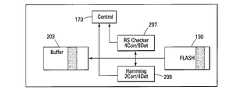
- FIG. 2shows a block diagram of one embodiment of an error detection and correction scheme for a memory device in accordance with the present invention.
- FIG. 3shows a table of results and accompanying actions resulting from the error detection in accordance with the embodiment of FIG. 2 .
- FIG. 4shows a block diagram of an embodiment of a Reed-Solomon code error correction scheme for a memory device in accordance with the embodiments of FIGS. 2 and 3 .
- FIG. 5shows a block diagram of another alternate embodiment of an error detection and correction scheme for a memory device in accordance with the present invention.
- FIG. 6shows a table of results and accompanying actions resulting from the error detection in accordance with the embodiment of FIG. 5 .
- FIG. 1illustrates a functional block diagram of a memory device 100 of one embodiment of the present invention that is coupled to a processor 110 .
- the processor 110may be a microprocessor, a processor, or some other type of controlling circuitry.
- the memory device 100 and the processor 110form part of an electronic system 120 .
- the memory device 100has been simplified to focus on features of the memory that are helpful in understanding the present invention.
- the memory deviceincludes an array of memory cells 130 .
- the memory cellsare non-volatile floating-gate memory cells and the memory array 130 is arranged in banks of rows and columns.
- An address buffer circuit 140is provided to latch address signals provided on address input connections A 0 -Ax 142 . Address signals are received and decoded by a row decoder 144 and a column decoder 146 to access the memory array 130 . It will be appreciated by those skilled in the art, with the benefit of the present description, that the number of address input connections depends on the density and architecture of the memory array 130 . That is, the number of addresses increases with both increased memory cell counts and increased bank and block counts.
- the memory device 100reads data in the memory array 130 by sensing voltage or current changes in the memory array columns using sense/buffer circuitry 150 .
- the sense/buffer circuitryin one embodiment, is coupled to read and latch a row of data from the memory array 130 .
- Data input and output buffer circuitry 160is included for bi-directional data communication over a plurality of data connections 162 with the controller 110 ).
- Write circuitry 155is provided to write data to the memory array.
- Control circuitry 170decodes signals provided on control connections 172 from the processor 110 . These signals are used to control the operations on the memory array 130 , including data read, data write, and erase operations. In one embodiment, the control circuitry 170 executes the error detection and correction schemes of the present invention.
- the control circuitry 170may be a state machine, a sequencer, or some other type of controller.
- FIG. 1The flash memory device illustrated in FIG. 1 has been simplified to facilitate a basic understanding of the features of the memory. A more detailed understanding of internal circuitry and functions of flash memories are known to those skilled in the art.
- FIG. 2illustrates a block diagram of one embodiment of an error detection and correction scheme for a memory device. This embodiment uses both the Hamming code and Reed-Solomon code error detection in parallel with the read operation to take advantage of the attributes of each scheme.
- a Reed-Solomon codeis an algebraic code that belongs to a class of Bose-Chaudhuri-Hocquenghem (BCH) multiple burst correcting cyclic codes.
- the Reed-Solomon codeoperates on bytes of fixed length. Given m parity symbols, a Reed-Solomon code can correct up to m byte errors in known positions that are also referred to as erasures. It can also detect and correct up to m/2 byte errors in unknown positions. In one embodiment, the Reed-Solomon code can immediately detect eight byte errors and correct four byte errors but typically requires some time to determine whether the errors are correctable. Reed-Solomon codes are well known in the art and are not discussed further.
- FIG. 2includes the flash memory array 130 as described above with reference to FIG. 1 .
- the operation of these cellsis well known in the art and is not discussed further.
- a data buffer 203is coupled to the flash memory array 130 .
- the data buffer 203is used by the memory controller circuit to store data after a read operation.
- the buffermay be the read/buffer 150 of FIG. 1 , memory in the controller circuit 170 , or some other temporary memory for storing data read from the memory array 201 .
- the controller circuit 170is responsible for performing the read operations and execution of the embodiments of the error detection and correction schemes of the present invention.
- the controller circuit 170also executes the Reed-Solomon and Hamming code error detection and correction operations.
- the method illustrated in FIG. 2performs a read operation into the buffer 203 .
- the datais being read out of the memory array 201 , it is simultaneously checked by both the Reed-Solomon 207 and Hamming 209 code checkers.
- the results from these error detection routines 207 and 209are passed to the controller circuitry 170 in order to determine the next course of action.
- FIG. 3illustrates a table that lists the combinations of results from each of the error detection routines 207 and 209 of FIG. 2 . Along with each combination of results is an action that is performed in response to that error detection combination.
- the first set of resultsis when both the Hamming code error detection and the Reed-Solomon code error detection determine that no errors exist in the data going to the buffer. In this case, the data is returned from the buffer to the memory array. Alternate embodiments may perform other tasks with the error-free data such as permitting the data to be read out of the buffer by a system controller coupled to the memory device.
- the Reed-Solomon code correction methodis then used as illustrated in FIG. 4 .
- FIG. 4illustrates a block diagram of the Reed-Solomon code correction method 207 after a detected error could not be corrected by the Hamming code error correction method 209 .
- the datais read from the buffer 203 and processed by the Reed-Solomon code correction method 207 .
- the resultsare sent to the controller circuitry 170 that returns the data to the buffer 203 if the errors were corrected. If the errors were not corrected, the data is permanently corrupted and flagged as such.
- the Hamming code error detectionmay detect an uncorrectable error (UE). This is an error that is beyond its error correction capabilities as described above. If the Reed-Solomon code error detection also detects an error, the Reed-Solomon code error correction method is used.
- UEuncorrectable error
- the Reed-Solomon code error correction methodis used to correct the error as illustrated in FIG. 4 .
- FIG. 5illustrates a block diagram of another embodiment of the error detection and correction scheme for a memory device in accordance with the present invention. This embodiment performs a serial error correction with the memory read operation.
- Datais loaded from the flash memory array 130 into the buffer 203 as part of a read operation. As the data is loaded, it is checked and corrected, if necessary, using the Hamming code error detection method 501 . If any errors are discovered during the error detection 501 , the Reed-Solomon code error detection method 502 is invoked. If necessary, the Reed-Solomon code error correction method 502 is performed.
- FIG. 6illustrates a table of results and accompanying actions resulting from the error detection in accordance with the embodiment of FIG. 5 . If the Hamming code error detection method does not find an error, the Reed-Solomon code correction/detection method is not invoked.
- the Reed-Solomon code correction methodis invoked to correct the data in the buffer using the Hamming correction data. The results from this operation are then run through the Reed-Solomon code error detection method again. The corrected data is then returned to the memory array from the buffer.
- the Hamming code error detection methodfinds an error that cannot be corrected using the Hamming code error correction method, the Reed-Solomon code error correction method is invoked. In this case, the Hamming correction data is not used by the Reed-Solomon code error correction method. The corrected data is then returned to the memory array from the buffer.
- the embodiments of the error detection and correction method in a memory deviceprovide a robust and efficient way to improve data reliability in a memory device. This is accomplished by using both the Hamming code and Reed-Solomon code error detection, either in parallel or in series with the data read operation. The repair operations then require very little overhead to perform.
- datais read from the memory array.
- a first error detection operationis performed in parallel with a second error detection operation on the read data.
- the results of the two error detection operationsare reported to the controller.
- the error corrected datais stored in the data buffer.
- a first error detection operationis performed as the data is loaded into a data buffer. If an error is detected that can be corrected by a first error correction operation, that operation is performed and a second error detection operation is used on the corrected data word. If the error is uncorrectable by the first error correction operation, the second error correction operation is used on the data word.
Landscapes
- Engineering & Computer Science (AREA)
- Theoretical Computer Science (AREA)
- Physics & Mathematics (AREA)
- Quality & Reliability (AREA)
- General Engineering & Computer Science (AREA)
- General Physics & Mathematics (AREA)
- Probability & Statistics with Applications (AREA)
- Techniques For Improving Reliability Of Storages (AREA)
- Error Detection And Correction (AREA)
Abstract
Description
Claims (19)
Priority Applications (2)
| Application Number | Priority Date | Filing Date | Title |
|---|---|---|---|
| US13/080,299US8661312B2 (en) | 2004-01-30 | 2011-04-05 | Error detection and correction scheme for a memory device |
| US14/173,256US8954818B2 (en) | 2004-01-30 | 2014-02-05 | Error detection and correction scheme for a memory device |
Applications Claiming Priority (3)
| Application Number | Priority Date | Filing Date | Title |
|---|---|---|---|
| US10/769,001US7389465B2 (en) | 2004-01-30 | 2004-01-30 | Error detection and correction scheme for a memory device |
| US11/706,506US7930612B2 (en) | 2004-01-30 | 2007-02-15 | Error detection and correction scheme for a memory device |
| US13/080,299US8661312B2 (en) | 2004-01-30 | 2011-04-05 | Error detection and correction scheme for a memory device |
Related Parent Applications (1)
| Application Number | Title | Priority Date | Filing Date |
|---|---|---|---|
| US11/706,506ContinuationUS7930612B2 (en) | 2004-01-30 | 2007-02-15 | Error detection and correction scheme for a memory device |
Related Child Applications (1)
| Application Number | Title | Priority Date | Filing Date |
|---|---|---|---|
| US14/173,256ContinuationUS8954818B2 (en) | 2004-01-30 | 2014-02-05 | Error detection and correction scheme for a memory device |
Publications (2)
| Publication Number | Publication Date |
|---|---|
| US20110185254A1 US20110185254A1 (en) | 2011-07-28 |
| US8661312B2true US8661312B2 (en) | 2014-02-25 |
Family
ID=34808013
Family Applications (4)
| Application Number | Title | Priority Date | Filing Date |
|---|---|---|---|
| US10/769,001Active2025-11-16US7389465B2 (en) | 2004-01-30 | 2004-01-30 | Error detection and correction scheme for a memory device |
| US11/706,506Active2027-02-02US7930612B2 (en) | 2004-01-30 | 2007-02-15 | Error detection and correction scheme for a memory device |
| US13/080,299Expired - LifetimeUS8661312B2 (en) | 2004-01-30 | 2011-04-05 | Error detection and correction scheme for a memory device |
| US14/173,256Expired - LifetimeUS8954818B2 (en) | 2004-01-30 | 2014-02-05 | Error detection and correction scheme for a memory device |
Family Applications Before (2)
| Application Number | Title | Priority Date | Filing Date |
|---|---|---|---|
| US10/769,001Active2025-11-16US7389465B2 (en) | 2004-01-30 | 2004-01-30 | Error detection and correction scheme for a memory device |
| US11/706,506Active2027-02-02US7930612B2 (en) | 2004-01-30 | 2007-02-15 | Error detection and correction scheme for a memory device |
Family Applications After (1)
| Application Number | Title | Priority Date | Filing Date |
|---|---|---|---|
| US14/173,256Expired - LifetimeUS8954818B2 (en) | 2004-01-30 | 2014-02-05 | Error detection and correction scheme for a memory device |
Country Status (3)
| Country | Link |
|---|---|
| US (4) | US7389465B2 (en) |
| TW (1) | TWI303435B (en) |
| WO (1) | WO2005076133A1 (en) |
Families Citing this family (168)
| Publication number | Priority date | Publication date | Assignee | Title |
|---|---|---|---|---|
| US7389465B2 (en)* | 2004-01-30 | 2008-06-17 | Micron Technology, Inc. | Error detection and correction scheme for a memory device |
| JP4695385B2 (en) | 2004-11-30 | 2011-06-08 | 株式会社東芝 | Memory card and card controller |
| GB2428496A (en)* | 2005-07-15 | 2007-01-31 | Global Silicon Ltd | Error correction for flash memory |
| US7523381B2 (en)* | 2005-09-01 | 2009-04-21 | Micron Technology, Inc. | Non-volatile memory with error detection |
| JP2009510585A (en)* | 2005-09-27 | 2009-03-12 | エヌエックスピー ビー ヴィ | Error detection / correction circuit and method |
| US7562283B2 (en) | 2005-12-27 | 2009-07-14 | D.S.P. Group Ltd. | Systems and methods for error correction using binary coded hexidecimal or hamming decoding |
| KR100746225B1 (en) | 2006-02-13 | 2007-08-03 | 삼성전자주식회사 | Semiconductor memory device and memory system having same |
| US7453723B2 (en)* | 2006-03-01 | 2008-11-18 | Micron Technology, Inc. | Memory with weighted multi-page read |
| FR2900749B1 (en)* | 2006-05-05 | 2008-07-25 | Thales Sa | METHOD AND DEVICE FOR SECURING THE MEMORY OF A COMPUTER AGAINST ERRORS DUE TO RADIATION |
| US7551486B2 (en)* | 2006-05-15 | 2009-06-23 | Apple Inc. | Iterative memory cell charging based on reference cell value |
| US7852690B2 (en)* | 2006-05-15 | 2010-12-14 | Apple Inc. | Multi-chip package for a flash memory |
| US7613043B2 (en)* | 2006-05-15 | 2009-11-03 | Apple Inc. | Shifting reference values to account for voltage sag |
| US7639542B2 (en)* | 2006-05-15 | 2009-12-29 | Apple Inc. | Maintenance operations for multi-level data storage cells |
| US8000134B2 (en) | 2006-05-15 | 2011-08-16 | Apple Inc. | Off-die charge pump that supplies multiple flash devices |
| US7568135B2 (en)* | 2006-05-15 | 2009-07-28 | Apple Inc. | Use of alternative value in cell detection |
| US7511646B2 (en)* | 2006-05-15 | 2009-03-31 | Apple Inc. | Use of 8-bit or higher A/D for NAND cell value |
| US7639531B2 (en)* | 2006-05-15 | 2009-12-29 | Apple Inc. | Dynamic cell bit resolution |
| US7911834B2 (en)* | 2006-05-15 | 2011-03-22 | Apple Inc. | Analog interface for a flash memory die |
| US7701797B2 (en)* | 2006-05-15 | 2010-04-20 | Apple Inc. | Two levels of voltage regulation supplied for logic and data programming voltage of a memory device |
| US20070283208A1 (en)* | 2006-06-01 | 2007-12-06 | International Business Machines Corporation | Systems, methods, and computer program products for providing a two-bit symbol bus error correcting code with bus diagnostic features |
| US20070283223A1 (en)* | 2006-06-01 | 2007-12-06 | International Business Machines Corporation | Systems, methods, and computer program products for providing a two-bit symbol bus error correcting code with all checkbits transferred last |
| US7721178B2 (en)* | 2006-06-01 | 2010-05-18 | International Business Machines Corporation | Systems, methods, and computer program products for providing a two-bit symbol bus error correcting code |
| US20070283207A1 (en)* | 2006-06-01 | 2007-12-06 | International Business Machines Corporation | Systems, methods, and computer program products for providing a two-bit symbol bus error correcting code with bus timing improvements |
| US7369434B2 (en)* | 2006-08-14 | 2008-05-06 | Micron Technology, Inc. | Flash memory with multi-bit read |
| DE102006040644A1 (en)* | 2006-08-30 | 2008-03-13 | Robert Bosch Gmbh | Correction procedure for a reprogrammable microprocessor |
| US9116823B2 (en) | 2006-12-06 | 2015-08-25 | Intelligent Intellectual Property Holdings 2 Llc | Systems and methods for adaptive error-correction coding |
| US9495241B2 (en)* | 2006-12-06 | 2016-11-15 | Longitude Enterprise Flash S.A.R.L. | Systems and methods for adaptive data storage |
| US8019938B2 (en) | 2006-12-06 | 2011-09-13 | Fusion-I0, Inc. | Apparatus, system, and method for solid-state storage as cache for high-capacity, non-volatile storage |
| US8015473B2 (en)* | 2006-12-19 | 2011-09-06 | Intel Corporation | Method, system, and apparatus for ECC protection of small data structures |
| US8055982B2 (en)* | 2007-02-21 | 2011-11-08 | Sigmatel, Inc. | Error correction system and method |
| US8051358B2 (en) | 2007-07-06 | 2011-11-01 | Micron Technology, Inc. | Error recovery storage along a nand-flash string |
| US8065583B2 (en) | 2007-07-06 | 2011-11-22 | Micron Technology, Inc. | Data storage with an outer block code and a stream-based inner code |
| US7747903B2 (en)* | 2007-07-09 | 2010-06-29 | Micron Technology, Inc. | Error correction for memory |
| JP4564520B2 (en) | 2007-08-31 | 2010-10-20 | 株式会社東芝 | Semiconductor memory device and control method thereof |
| US8327245B2 (en) | 2007-11-21 | 2012-12-04 | Micron Technology, Inc. | Memory controller supporting rate-compatible punctured codes |
| US8046542B2 (en) | 2007-11-21 | 2011-10-25 | Micron Technology, Inc. | Fault-tolerant non-volatile integrated circuit memory |
| US7836226B2 (en) | 2007-12-06 | 2010-11-16 | Fusion-Io, Inc. | Apparatus, system, and method for coordinating storage requests in a multi-processor/multi-thread environment |
| US20090158122A1 (en)* | 2007-12-12 | 2009-06-18 | Intel Corporation | Forward error correction of an error acknowledgement command protocol |
| US8762620B2 (en)* | 2007-12-27 | 2014-06-24 | Sandisk Enterprise Ip Llc | Multiprocessor storage controller |
| TWI364661B (en)* | 2008-09-25 | 2012-05-21 | Silicon Motion Inc | Access methods for a flash memory and memory devices |
| EP2359372B1 (en)* | 2008-12-18 | 2020-04-08 | NovaChips Canada Inc. | Error detection method and a system including one or more memory devices |
| US20100180182A1 (en)* | 2009-01-09 | 2010-07-15 | Seagate Technology Llc | Data memory device and controller with interface error detection and handling logic |
| KR20100098969A (en)* | 2009-03-02 | 2010-09-10 | 삼성전자주식회사 | Semiconductor device for improving reliability of error correction codes, semiconductor system having the same, and method for processing error correction code |
| CN101615145B (en)* | 2009-07-24 | 2011-12-07 | 中兴通讯股份有限公司 | Method and device for improving reliability of data caching of memorizer |
| US8077515B2 (en) | 2009-08-25 | 2011-12-13 | Micron Technology, Inc. | Methods, devices, and systems for dealing with threshold voltage change in memory devices |
| US8271697B2 (en) | 2009-09-29 | 2012-09-18 | Micron Technology, Inc. | State change in systems having devices coupled in a chained configuration |
| US9626243B2 (en)* | 2009-12-11 | 2017-04-18 | Advanced Micro Devices, Inc. | Data error correction device and methods thereof |
| TWI413904B (en)* | 2010-03-03 | 2013-11-01 | Pixart Imaging Inc | Universal Serial Bus (USB) controller and its execution method |
| JP4772909B1 (en)* | 2010-03-30 | 2011-09-14 | 株式会社東芝 | Information processing apparatus and information processing method |
| US8429391B2 (en) | 2010-04-16 | 2013-04-23 | Micron Technology, Inc. | Boot partitions in memory devices and systems |
| US8451664B2 (en) | 2010-05-12 | 2013-05-28 | Micron Technology, Inc. | Determining and using soft data in memory devices and systems |
| US8386895B2 (en) | 2010-05-19 | 2013-02-26 | Micron Technology, Inc. | Enhanced multilevel memory |
| US8640005B2 (en)* | 2010-05-21 | 2014-01-28 | Intel Corporation | Method and apparatus for using cache memory in a system that supports a low power state |
| KR101739878B1 (en) | 2011-02-22 | 2017-05-26 | 삼성전자주식회사 | Controller, method of operating the controller, and memory system having the controller |
| US8677205B2 (en) | 2011-03-10 | 2014-03-18 | Freescale Semiconductor, Inc. | Hierarchical error correction for large memories |
| US8909982B2 (en) | 2011-06-19 | 2014-12-09 | Sandisk Enterprise Ip Llc | System and method for detecting copyback programming problems |
| US8910020B2 (en) | 2011-06-19 | 2014-12-09 | Sandisk Enterprise Ip Llc | Intelligent bit recovery for flash memory |
| CN102231136B (en)* | 2011-07-12 | 2014-06-11 | 晨星软件研发(深圳)有限公司 | Data storage method and device for flash memory storage equipment |
| US8938658B2 (en) | 2011-11-07 | 2015-01-20 | Sandisk Enterprise Ip Llc | Statistical read comparison signal generation for memory systems |
| US8954822B2 (en) | 2011-11-18 | 2015-02-10 | Sandisk Enterprise Ip Llc | Data encoder and decoder using memory-specific parity-check matrix |
| US8924815B2 (en) | 2011-11-18 | 2014-12-30 | Sandisk Enterprise Ip Llc | Systems, methods and devices for decoding codewords having multiple parity segments |
| US9048876B2 (en) | 2011-11-18 | 2015-06-02 | Sandisk Enterprise Ip Llc | Systems, methods and devices for multi-tiered error correction |
| US8914712B2 (en) | 2012-02-27 | 2014-12-16 | Freescale Semiconductor, Inc. | Hierarchical error correction |
| US8806294B2 (en) | 2012-04-20 | 2014-08-12 | Freescale Semiconductor, Inc. | Error detection within a memory |
| US9047214B1 (en) | 2012-05-22 | 2015-06-02 | Pmc-Sierra, Inc. | System and method for tolerating a failed page in a flash device |
| US9021337B1 (en) | 2012-05-22 | 2015-04-28 | Pmc-Sierra, Inc. | Systems and methods for adaptively selecting among different error correction coding schemes in a flash drive |
| US9176812B1 (en) | 2012-05-22 | 2015-11-03 | Pmc-Sierra, Inc. | Systems and methods for storing data in page stripes of a flash drive |
| US9021336B1 (en) | 2012-05-22 | 2015-04-28 | Pmc-Sierra, Inc. | Systems and methods for redundantly storing error correction codes in a flash drive with secondary parity information spread out across each page of a group of pages |
| US8793556B1 (en) | 2012-05-22 | 2014-07-29 | Pmc-Sierra, Inc. | Systems and methods for reclaiming flash blocks of a flash drive |
| US8972824B1 (en) | 2012-05-22 | 2015-03-03 | Pmc-Sierra, Inc. | Systems and methods for transparently varying error correction code strength in a flash drive |
| US9183085B1 (en) | 2012-05-22 | 2015-11-10 | Pmc-Sierra, Inc. | Systems and methods for adaptively selecting from among a plurality of error correction coding schemes in a flash drive for robustness and low latency |
| US8996957B1 (en) | 2012-05-22 | 2015-03-31 | Pmc-Sierra, Inc. | Systems and methods for initializing regions of a flash drive having diverse error correction coding (ECC) schemes |
| US9021333B1 (en) | 2012-05-22 | 2015-04-28 | Pmc-Sierra, Inc. | Systems and methods for recovering data from failed portions of a flash drive |
| US8788910B1 (en) | 2012-05-22 | 2014-07-22 | Pmc-Sierra, Inc. | Systems and methods for low latency, high reliability error correction in a flash drive |
| CN104246898B (en)* | 2012-05-31 | 2017-03-22 | 慧与发展有限责任合伙企业 | local error detection and global error correction |
| TWI475387B (en)* | 2012-07-19 | 2015-03-01 | Jmicron Technology Corp | Memory control method and memory control circuit thereof |
| US9699263B1 (en) | 2012-08-17 | 2017-07-04 | Sandisk Technologies Llc. | Automatic read and write acceleration of data accessed by virtual machines |
| US9577673B2 (en) | 2012-11-08 | 2017-02-21 | Micron Technology, Inc. | Error correction methods and apparatuses using first and second decoders |
| US9501398B2 (en) | 2012-12-26 | 2016-11-22 | Sandisk Technologies Llc | Persistent storage device with NVRAM for staging writes |
| US9239751B1 (en) | 2012-12-27 | 2016-01-19 | Sandisk Enterprise Ip Llc | Compressing data from multiple reads for error control management in memory systems |
| US9612948B2 (en) | 2012-12-27 | 2017-04-04 | Sandisk Technologies Llc | Reads and writes between a contiguous data block and noncontiguous sets of logical address blocks in a persistent storage device |
| US9003264B1 (en) | 2012-12-31 | 2015-04-07 | Sandisk Enterprise Ip Llc | Systems, methods, and devices for multi-dimensional flash RAID data protection |
| US9454420B1 (en) | 2012-12-31 | 2016-09-27 | Sandisk Technologies Llc | Method and system of reading threshold voltage equalization |
| US9329928B2 (en) | 2013-02-20 | 2016-05-03 | Sandisk Enterprise IP LLC. | Bandwidth optimization in a non-volatile memory system |
| US9214965B2 (en) | 2013-02-20 | 2015-12-15 | Sandisk Enterprise Ip Llc | Method and system for improving data integrity in non-volatile storage |
| US9870830B1 (en) | 2013-03-14 | 2018-01-16 | Sandisk Technologies Llc | Optimal multilevel sensing for reading data from a storage medium |
| US9053012B1 (en) | 2013-03-15 | 2015-06-09 | Pmc-Sierra, Inc. | Systems and methods for storing data for solid-state memory |
| US9244763B1 (en) | 2013-03-15 | 2016-01-26 | Sandisk Enterprise Ip Llc | System and method for updating a reading threshold voltage based on symbol transition information |
| US9208018B1 (en) | 2013-03-15 | 2015-12-08 | Pmc-Sierra, Inc. | Systems and methods for reclaiming memory for solid-state memory |
| US9009565B1 (en) | 2013-03-15 | 2015-04-14 | Pmc-Sierra, Inc. | Systems and methods for mapping for solid-state memory |
| US9009576B1 (en) | 2013-03-15 | 2015-04-14 | Sandisk Enterprise Ip Llc | Adaptive LLR based on syndrome weight |
| US9136877B1 (en) | 2013-03-15 | 2015-09-15 | Sandisk Enterprise Ip Llc | Syndrome layered decoding for LDPC codes |
| US9367246B2 (en) | 2013-03-15 | 2016-06-14 | Sandisk Technologies Inc. | Performance optimization of data transfer for soft information generation |
| US9092350B1 (en) | 2013-03-15 | 2015-07-28 | Sandisk Enterprise Ip Llc | Detection and handling of unbalanced errors in interleaved codewords |
| US9081701B1 (en) | 2013-03-15 | 2015-07-14 | Pmc-Sierra, Inc. | Systems and methods for decoding data for solid-state memory |
| US9236886B1 (en) | 2013-03-15 | 2016-01-12 | Sandisk Enterprise Ip Llc | Universal and reconfigurable QC-LDPC encoder |
| US9026867B1 (en) | 2013-03-15 | 2015-05-05 | Pmc-Sierra, Inc. | Systems and methods for adapting to changing characteristics of multi-level cells in solid-state memory |
| US10049037B2 (en) | 2013-04-05 | 2018-08-14 | Sandisk Enterprise Ip Llc | Data management in a storage system |
| US9170941B2 (en) | 2013-04-05 | 2015-10-27 | Sandisk Enterprises IP LLC | Data hardening in a storage system |
| US9159437B2 (en) | 2013-06-11 | 2015-10-13 | Sandisk Enterprise IP LLC. | Device and method for resolving an LM flag issue |
| TWI497280B (en)* | 2013-07-08 | 2015-08-21 | Phison Electronics Corp | Data protecting method, memory storage device and memory controller |
| US9384126B1 (en) | 2013-07-25 | 2016-07-05 | Sandisk Technologies Inc. | Methods and systems to avoid false negative results in bloom filters implemented in non-volatile data storage systems |
| US9043517B1 (en) | 2013-07-25 | 2015-05-26 | Sandisk Enterprise Ip Llc | Multipass programming in buffers implemented in non-volatile data storage systems |
| US9524235B1 (en) | 2013-07-25 | 2016-12-20 | Sandisk Technologies Llc | Local hash value generation in non-volatile data storage systems |
| WO2015016880A1 (en)* | 2013-07-31 | 2015-02-05 | Hewlett-Packard Development Company, L.P. | Global error correction |
| TWI479359B (en)* | 2013-08-01 | 2015-04-01 | Phison Electronics Corp | Command executing method, memory controller and memory storage apparatus |
| KR102170857B1 (en)* | 2013-08-19 | 2020-10-29 | 삼성전자주식회사 | Driving method of nonvolatile memory device using variable resistive element |
| US9639463B1 (en) | 2013-08-26 | 2017-05-02 | Sandisk Technologies Llc | Heuristic aware garbage collection scheme in storage systems |
| US9361221B1 (en) | 2013-08-26 | 2016-06-07 | Sandisk Technologies Inc. | Write amplification reduction through reliable writes during garbage collection |
| US9442670B2 (en) | 2013-09-03 | 2016-09-13 | Sandisk Technologies Llc | Method and system for rebalancing data stored in flash memory devices |
| US9519577B2 (en) | 2013-09-03 | 2016-12-13 | Sandisk Technologies Llc | Method and system for migrating data between flash memory devices |
| KR101767018B1 (en) | 2013-09-27 | 2017-08-09 | 인텔 코포레이션 | Error correction in non_volatile memory |
| US9158349B2 (en) | 2013-10-04 | 2015-10-13 | Sandisk Enterprise Ip Llc | System and method for heat dissipation |
| US9323637B2 (en) | 2013-10-07 | 2016-04-26 | Sandisk Enterprise Ip Llc | Power sequencing and data hardening architecture |
| US9298608B2 (en) | 2013-10-18 | 2016-03-29 | Sandisk Enterprise Ip Llc | Biasing for wear leveling in storage systems |
| US9442662B2 (en) | 2013-10-18 | 2016-09-13 | Sandisk Technologies Llc | Device and method for managing die groups |
| US9436831B2 (en) | 2013-10-30 | 2016-09-06 | Sandisk Technologies Llc | Secure erase in a memory device |
| US9263156B2 (en) | 2013-11-07 | 2016-02-16 | Sandisk Enterprise Ip Llc | System and method for adjusting trip points within a storage device |
| US9244785B2 (en) | 2013-11-13 | 2016-01-26 | Sandisk Enterprise Ip Llc | Simulated power failure and data hardening |
| US9152555B2 (en) | 2013-11-15 | 2015-10-06 | Sandisk Enterprise IP LLC. | Data management with modular erase in a data storage system |
| US9703816B2 (en) | 2013-11-19 | 2017-07-11 | Sandisk Technologies Llc | Method and system for forward reference logging in a persistent datastore |
| US9520197B2 (en) | 2013-11-22 | 2016-12-13 | Sandisk Technologies Llc | Adaptive erase of a storage device |
| US9280429B2 (en) | 2013-11-27 | 2016-03-08 | Sandisk Enterprise Ip Llc | Power fail latching based on monitoring multiple power supply voltages in a storage device |
| US9122636B2 (en) | 2013-11-27 | 2015-09-01 | Sandisk Enterprise Ip Llc | Hard power fail architecture |
| US9520162B2 (en) | 2013-11-27 | 2016-12-13 | Sandisk Technologies Llc | DIMM device controller supervisor |
| US9582058B2 (en) | 2013-11-29 | 2017-02-28 | Sandisk Technologies Llc | Power inrush management of storage devices |
| US9250676B2 (en) | 2013-11-29 | 2016-02-02 | Sandisk Enterprise Ip Llc | Power failure architecture and verification |
| US9092370B2 (en) | 2013-12-03 | 2015-07-28 | Sandisk Enterprise Ip Llc | Power failure tolerant cryptographic erase |
| US9235245B2 (en) | 2013-12-04 | 2016-01-12 | Sandisk Enterprise Ip Llc | Startup performance and power isolation |
| US9129665B2 (en) | 2013-12-17 | 2015-09-08 | Sandisk Enterprise Ip Llc | Dynamic brownout adjustment in a storage device |
| US9323602B2 (en) | 2014-01-20 | 2016-04-26 | Freescale Semiconductor, Inc. | Error correction with extended CAM |
| US9549457B2 (en) | 2014-02-12 | 2017-01-17 | Sandisk Technologies Llc | System and method for redirecting airflow across an electronic assembly |
| US9497889B2 (en) | 2014-02-27 | 2016-11-15 | Sandisk Technologies Llc | Heat dissipation for substrate assemblies |
| US9703636B2 (en) | 2014-03-01 | 2017-07-11 | Sandisk Technologies Llc | Firmware reversion trigger and control |
| US9348377B2 (en) | 2014-03-14 | 2016-05-24 | Sandisk Enterprise Ip Llc | Thermal isolation techniques |
| US9485851B2 (en) | 2014-03-14 | 2016-11-01 | Sandisk Technologies Llc | Thermal tube assembly structures |
| US9519319B2 (en) | 2014-03-14 | 2016-12-13 | Sandisk Technologies Llc | Self-supporting thermal tube structure for electronic assemblies |
| US9448876B2 (en) | 2014-03-19 | 2016-09-20 | Sandisk Technologies Llc | Fault detection and prediction in storage devices |
| US9454448B2 (en) | 2014-03-19 | 2016-09-27 | Sandisk Technologies Llc | Fault testing in storage devices |
| US9390814B2 (en) | 2014-03-19 | 2016-07-12 | Sandisk Technologies Llc | Fault detection and prediction for data storage elements |
| US9626400B2 (en) | 2014-03-31 | 2017-04-18 | Sandisk Technologies Llc | Compaction of information in tiered data structure |
| US9626399B2 (en) | 2014-03-31 | 2017-04-18 | Sandisk Technologies Llc | Conditional updates for reducing frequency of data modification operations |
| US9390021B2 (en) | 2014-03-31 | 2016-07-12 | Sandisk Technologies Llc | Efficient cache utilization in a tiered data structure |
| US9697267B2 (en) | 2014-04-03 | 2017-07-04 | Sandisk Technologies Llc | Methods and systems for performing efficient snapshots in tiered data structures |
| US9396064B2 (en) | 2014-04-30 | 2016-07-19 | Freescale Semiconductor, Inc. | Error correction with secondary memory |
| US10656840B2 (en) | 2014-05-30 | 2020-05-19 | Sandisk Technologies Llc | Real-time I/O pattern recognition to enhance performance and endurance of a storage device |
| US9070481B1 (en) | 2014-05-30 | 2015-06-30 | Sandisk Technologies Inc. | Internal current measurement for age measurements |
| US10146448B2 (en) | 2014-05-30 | 2018-12-04 | Sandisk Technologies Llc | Using history of I/O sequences to trigger cached read ahead in a non-volatile storage device |
| US9645749B2 (en) | 2014-05-30 | 2017-05-09 | Sandisk Technologies Llc | Method and system for recharacterizing the storage density of a memory device or a portion thereof |
| US10162748B2 (en) | 2014-05-30 | 2018-12-25 | Sandisk Technologies Llc | Prioritizing garbage collection and block allocation based on I/O history for logical address regions |
| US9703491B2 (en) | 2014-05-30 | 2017-07-11 | Sandisk Technologies Llc | Using history of unaligned writes to cache data and avoid read-modify-writes in a non-volatile storage device |
| US10114557B2 (en) | 2014-05-30 | 2018-10-30 | Sandisk Technologies Llc | Identification of hot regions to enhance performance and endurance of a non-volatile storage device |
| US8891303B1 (en) | 2014-05-30 | 2014-11-18 | Sandisk Technologies Inc. | Method and system for dynamic word line based configuration of a three-dimensional memory device |
| US9093160B1 (en) | 2014-05-30 | 2015-07-28 | Sandisk Technologies Inc. | Methods and systems for staggered memory operations |
| US10372613B2 (en) | 2014-05-30 | 2019-08-06 | Sandisk Technologies Llc | Using sub-region I/O history to cache repeatedly accessed sub-regions in a non-volatile storage device |
| US10656842B2 (en) | 2014-05-30 | 2020-05-19 | Sandisk Technologies Llc | Using history of I/O sizes and I/O sequences to trigger coalesced writes in a non-volatile storage device |
| US9652381B2 (en) | 2014-06-19 | 2017-05-16 | Sandisk Technologies Llc | Sub-block garbage collection |
| JP6332134B2 (en)* | 2014-09-16 | 2018-05-30 | 株式会社デンソー | Memory diagnostic circuit |
| US9768808B2 (en) | 2015-04-08 | 2017-09-19 | Sandisk Technologies Llc | Method for modifying device-specific variable error correction settings |
| US9606737B2 (en) | 2015-05-20 | 2017-03-28 | Sandisk Technologies Llc | Variable bit encoding per NAND flash cell to extend life of flash-based storage devices and preserve over-provisioning |
| US9639282B2 (en) | 2015-05-20 | 2017-05-02 | Sandisk Technologies Llc | Variable bit encoding per NAND flash cell to improve device endurance and extend life of flash-based storage devices |
| US10013179B2 (en) | 2015-12-03 | 2018-07-03 | Sandisk Technologies Llc | Reading logical groups of data from physical locations in memory using headers |
| US9830084B2 (en) | 2015-12-03 | 2017-11-28 | Sandisk Technologies Llc | Writing logical groups of data to physical locations in memory using headers |
| GB201710839D0 (en)* | 2017-07-05 | 2017-08-16 | Irdeto Bv | Data protection |
| CN109903806A (en)* | 2019-04-01 | 2019-06-18 | 江苏华存电子科技有限公司 | A kind of double mode error detection memory and double mode error-detecting method |
| JP7306945B2 (en)* | 2019-10-03 | 2023-07-11 | ファナック株式会社 | MEMORY ERROR DETERMINATION DEVICE AND COMPUTER PROGRAM FOR MEMORY ERROR DETERMINATION |
| TWI847532B (en)* | 2023-02-08 | 2024-07-01 | 南亞科技股份有限公司 | Memory system and memory testing method |
| US12308855B2 (en) | 2023-04-11 | 2025-05-20 | Sk Hynix Nand Product Solutions Corp. | Methods and systems for error-detecting during iterative decoding |
Citations (11)
| Publication number | Priority date | Publication date | Assignee | Title |
|---|---|---|---|---|
| US4005405A (en) | 1975-05-07 | 1977-01-25 | Data General Corporation | Error detection and correction in data processing systems |
| US4716566A (en) | 1984-08-20 | 1987-12-29 | Nec Corporation | Error correcting system |
| US4716567A (en) | 1985-02-08 | 1987-12-29 | Hitachi, Ltd. | Method of transmitting digital data in which error detection codes are dispersed using alternate delay times |
| US5357527A (en) | 1992-12-31 | 1994-10-18 | Trimble Navigation Limited | Validation of RAM-resident software programs |
| US5754563A (en) | 1995-09-11 | 1998-05-19 | Ecc Technologies, Inc. | Byte-parallel system for implementing reed-solomon error-correcting codes |
| US5754753A (en) | 1992-06-11 | 1998-05-19 | Digital Equipment Corporation | Multiple-bit error correction in computer main memory |
| US6003151A (en) | 1997-02-04 | 1999-12-14 | Mediatek Inc. | Error correction and detection system for mass storage controller |
| US6651212B1 (en) | 1999-12-16 | 2003-11-18 | Hitachi, Ltd. | Recording/reproduction device, semiconductor memory, and memory card using the semiconductor memory |
| US6769087B2 (en) | 2000-04-11 | 2004-07-27 | Kabushiki Kaisha Toshiba | Data storage device and method for controlling the device |
| US7231585B2 (en) | 2002-12-11 | 2007-06-12 | Nvidia Corporation | Error correction for flash memory |
| US7389465B2 (en)* | 2004-01-30 | 2008-06-17 | Micron Technology, Inc. | Error detection and correction scheme for a memory device |
Family Cites Families (10)
| Publication number | Priority date | Publication date | Assignee | Title |
|---|---|---|---|---|
| US4359772A (en)* | 1980-11-14 | 1982-11-16 | International Business Machines Corporation | Dual function error correcting system |
| US4464747A (en)* | 1982-02-18 | 1984-08-07 | The Singer Company | High reliability memory |
| US4464755A (en)* | 1982-03-26 | 1984-08-07 | Rca Corporation | Memory system with error detection and correction |
| US4547882A (en)* | 1983-03-01 | 1985-10-15 | The Board Of Trustees Of The Leland Stanford Jr. University | Error detecting and correcting memories |
| US4617664A (en)* | 1984-06-29 | 1986-10-14 | International Business Machines Corporation | Error correction for multiple bit output chips |
| US5513192A (en)* | 1992-08-28 | 1996-04-30 | Sun Microsystems, Inc. | Fault tolerant disk drive system with error detection and correction |
| US5384788A (en)* | 1992-10-26 | 1995-01-24 | Dell Usa, L.P. | Apparatus and method for optimal error correcting code to parity conversion |
| US5602857A (en)* | 1993-09-21 | 1997-02-11 | Cirrus Logic, Inc. | Error correction method and apparatus |
| JP2001027953A (en)* | 1999-07-15 | 2001-01-30 | Mitsubishi Electric Corp | Semiconductor storage device |
| US7028213B2 (en)* | 2001-09-28 | 2006-04-11 | Hewlett-Packard Development Company, L.P. | Error indication in a raid memory system |
- 2004
- 2004-01-30USUS10/769,001patent/US7389465B2/enactiveActive
- 2005
- 2005-01-26WOPCT/US2005/002496patent/WO2005076133A1/enactiveApplication Filing
- 2005-01-28TWTW094102574Apatent/TWI303435B/ennot_activeIP Right Cessation
- 2007
- 2007-02-15USUS11/706,506patent/US7930612B2/enactiveActive
- 2011
- 2011-04-05USUS13/080,299patent/US8661312B2/ennot_activeExpired - Lifetime
- 2014
- 2014-02-05USUS14/173,256patent/US8954818B2/ennot_activeExpired - Lifetime
Patent Citations (11)
| Publication number | Priority date | Publication date | Assignee | Title |
|---|---|---|---|---|
| US4005405A (en) | 1975-05-07 | 1977-01-25 | Data General Corporation | Error detection and correction in data processing systems |
| US4716566A (en) | 1984-08-20 | 1987-12-29 | Nec Corporation | Error correcting system |
| US4716567A (en) | 1985-02-08 | 1987-12-29 | Hitachi, Ltd. | Method of transmitting digital data in which error detection codes are dispersed using alternate delay times |
| US5754753A (en) | 1992-06-11 | 1998-05-19 | Digital Equipment Corporation | Multiple-bit error correction in computer main memory |
| US5357527A (en) | 1992-12-31 | 1994-10-18 | Trimble Navigation Limited | Validation of RAM-resident software programs |
| US5754563A (en) | 1995-09-11 | 1998-05-19 | Ecc Technologies, Inc. | Byte-parallel system for implementing reed-solomon error-correcting codes |
| US6003151A (en) | 1997-02-04 | 1999-12-14 | Mediatek Inc. | Error correction and detection system for mass storage controller |
| US6651212B1 (en) | 1999-12-16 | 2003-11-18 | Hitachi, Ltd. | Recording/reproduction device, semiconductor memory, and memory card using the semiconductor memory |
| US6769087B2 (en) | 2000-04-11 | 2004-07-27 | Kabushiki Kaisha Toshiba | Data storage device and method for controlling the device |
| US7231585B2 (en) | 2002-12-11 | 2007-06-12 | Nvidia Corporation | Error correction for flash memory |
| US7389465B2 (en)* | 2004-01-30 | 2008-06-17 | Micron Technology, Inc. | Error detection and correction scheme for a memory device |
Also Published As
| Publication number | Publication date |
|---|---|
| US20070162824A1 (en) | 2007-07-12 |
| US20140189475A1 (en) | 2014-07-03 |
| US8954818B2 (en) | 2015-02-10 |
| US20050172207A1 (en) | 2005-08-04 |
| TWI303435B (en) | 2008-11-21 |
| WO2005076133A1 (en) | 2005-08-18 |
| US7930612B2 (en) | 2011-04-19 |
| US20110185254A1 (en) | 2011-07-28 |
| US7389465B2 (en) | 2008-06-17 |
| TW200532703A (en) | 2005-10-01 |
Similar Documents
| Publication | Publication Date | Title |
|---|---|---|
| US8661312B2 (en) | Error detection and correction scheme for a memory device | |
| US12413251B2 (en) | Semiconductor memory device and method of controlling the same | |
| EP2203819B1 (en) | Semiconductor memory device and its control method | |
| KR100681429B1 (en) | Semiconductor memory device and bit error detection method thereof | |
| US8161355B2 (en) | Automatic refresh for improving data retention and endurance characteristics of an embedded non-volatile memory in a standard CMOS logic process | |
| US20060069851A1 (en) | Integrated circuit memory devices that support detection of write errors occuring during power failures and methods of operating same | |
| US7747926B2 (en) | Methods and apparatus for a memory device with self-healing reference bits | |
| US12212339B2 (en) | Error correction circuit, memory system, and error correction method | |
| US9280412B2 (en) | Memory with error correction configured to prevent overcorrection |
Legal Events
| Date | Code | Title | Description |
|---|---|---|---|
| FEPP | Fee payment procedure | Free format text:PAYOR NUMBER ASSIGNED (ORIGINAL EVENT CODE: ASPN); ENTITY STATUS OF PATENT OWNER: LARGE ENTITY | |
| STCF | Information on status: patent grant | Free format text:PATENTED CASE | |
| AS | Assignment | Owner name:U.S. BANK NATIONAL ASSOCIATION, AS COLLATERAL AGENT, CALIFORNIA Free format text:SECURITY INTEREST;ASSIGNOR:MICRON TECHNOLOGY, INC.;REEL/FRAME:038669/0001 Effective date:20160426 Owner name:U.S. BANK NATIONAL ASSOCIATION, AS COLLATERAL AGEN Free format text:SECURITY INTEREST;ASSIGNOR:MICRON TECHNOLOGY, INC.;REEL/FRAME:038669/0001 Effective date:20160426 | |
| AS | Assignment | Owner name:MORGAN STANLEY SENIOR FUNDING, INC., AS COLLATERAL AGENT, MARYLAND Free format text:PATENT SECURITY AGREEMENT;ASSIGNOR:MICRON TECHNOLOGY, INC.;REEL/FRAME:038954/0001 Effective date:20160426 Owner name:MORGAN STANLEY SENIOR FUNDING, INC., AS COLLATERAL Free format text:PATENT SECURITY AGREEMENT;ASSIGNOR:MICRON TECHNOLOGY, INC.;REEL/FRAME:038954/0001 Effective date:20160426 | |
| AS | Assignment | Owner name:U.S. BANK NATIONAL ASSOCIATION, AS COLLATERAL AGENT, CALIFORNIA Free format text:CORRECTIVE ASSIGNMENT TO CORRECT THE REPLACE ERRONEOUSLY FILED PATENT #7358718 WITH THE CORRECT PATENT #7358178 PREVIOUSLY RECORDED ON REEL 038669 FRAME 0001. ASSIGNOR(S) HEREBY CONFIRMS THE SECURITY INTEREST;ASSIGNOR:MICRON TECHNOLOGY, INC.;REEL/FRAME:043079/0001 Effective date:20160426 Owner name:U.S. BANK NATIONAL ASSOCIATION, AS COLLATERAL AGEN Free format text:CORRECTIVE ASSIGNMENT TO CORRECT THE REPLACE ERRONEOUSLY FILED PATENT #7358718 WITH THE CORRECT PATENT #7358178 PREVIOUSLY RECORDED ON REEL 038669 FRAME 0001. ASSIGNOR(S) HEREBY CONFIRMS THE SECURITY INTEREST;ASSIGNOR:MICRON TECHNOLOGY, INC.;REEL/FRAME:043079/0001 Effective date:20160426 | |
| FPAY | Fee payment | Year of fee payment:4 | |
| AS | Assignment | Owner name:JPMORGAN CHASE BANK, N.A., AS COLLATERAL AGENT, ILLINOIS Free format text:SECURITY INTEREST;ASSIGNORS:MICRON TECHNOLOGY, INC.;MICRON SEMICONDUCTOR PRODUCTS, INC.;REEL/FRAME:047540/0001 Effective date:20180703 Owner name:JPMORGAN CHASE BANK, N.A., AS COLLATERAL AGENT, IL Free format text:SECURITY INTEREST;ASSIGNORS:MICRON TECHNOLOGY, INC.;MICRON SEMICONDUCTOR PRODUCTS, INC.;REEL/FRAME:047540/0001 Effective date:20180703 | |
| AS | Assignment | Owner name:MICRON TECHNOLOGY, INC., IDAHO Free format text:RELEASE BY SECURED PARTY;ASSIGNOR:U.S. BANK NATIONAL ASSOCIATION, AS COLLATERAL AGENT;REEL/FRAME:047243/0001 Effective date:20180629 | |
| AS | Assignment | Owner name:MICRON TECHNOLOGY, INC., IDAHO Free format text:RELEASE BY SECURED PARTY;ASSIGNOR:MORGAN STANLEY SENIOR FUNDING, INC., AS COLLATERAL AGENT;REEL/FRAME:050937/0001 Effective date:20190731 | |
| AS | Assignment | Owner name:MICRON SEMICONDUCTOR PRODUCTS, INC., IDAHO Free format text:RELEASE BY SECURED PARTY;ASSIGNOR:JPMORGAN CHASE BANK, N.A., AS COLLATERAL AGENT;REEL/FRAME:051028/0001 Effective date:20190731 Owner name:MICRON TECHNOLOGY, INC., IDAHO Free format text:RELEASE BY SECURED PARTY;ASSIGNOR:JPMORGAN CHASE BANK, N.A., AS COLLATERAL AGENT;REEL/FRAME:051028/0001 Effective date:20190731 | |
| MAFP | Maintenance fee payment | Free format text:PAYMENT OF MAINTENANCE FEE, 8TH YEAR, LARGE ENTITY (ORIGINAL EVENT CODE: M1552); ENTITY STATUS OF PATENT OWNER: LARGE ENTITY Year of fee payment:8 | |
| MAFP | Maintenance fee payment | Free format text:PAYMENT OF MAINTENANCE FEE, 12TH YEAR, LARGE ENTITY (ORIGINAL EVENT CODE: M1553); ENTITY STATUS OF PATENT OWNER: LARGE ENTITY Year of fee payment:12 |