US8659929B2 - Amorphous silicon RRAM with non-linear device and operation - Google Patents
Amorphous silicon RRAM with non-linear device and operationDownload PDFInfo
- Publication number
- US8659929B2 US8659929B2US13/174,264US201113174264AUS8659929B2US 8659929 B2US8659929 B2US 8659929B2US 201113174264 AUS201113174264 AUS 201113174264AUS 8659929 B2US8659929 B2US 8659929B2
- Authority
- US
- United States
- Prior art keywords
- electrode
- voltage
- resistive switching
- state
- linear
- Prior art date
- Legal status (The legal status is an assumption and is not a legal conclusion. Google has not performed a legal analysis and makes no representation as to the accuracy of the status listed.)
- Active, expires
Links
Images


Classifications
- G—PHYSICS
- G11—INFORMATION STORAGE
- G11C—STATIC STORES
- G11C13/00—Digital stores characterised by the use of storage elements not covered by groups G11C11/00, G11C23/00, or G11C25/00
- G11C13/0002—Digital stores characterised by the use of storage elements not covered by groups G11C11/00, G11C23/00, or G11C25/00 using resistive RAM [RRAM] elements
- G11C13/0021—Auxiliary circuits
- G11C13/004—Reading or sensing circuits or methods
- G—PHYSICS
- G11—INFORMATION STORAGE
- G11C—STATIC STORES
- G11C13/00—Digital stores characterised by the use of storage elements not covered by groups G11C11/00, G11C23/00, or G11C25/00
- G11C13/0002—Digital stores characterised by the use of storage elements not covered by groups G11C11/00, G11C23/00, or G11C25/00 using resistive RAM [RRAM] elements
- G11C13/0007—Digital stores characterised by the use of storage elements not covered by groups G11C11/00, G11C23/00, or G11C25/00 using resistive RAM [RRAM] elements comprising metal oxide memory material, e.g. perovskites
- G—PHYSICS
- G11—INFORMATION STORAGE
- G11C—STATIC STORES
- G11C13/00—Digital stores characterised by the use of storage elements not covered by groups G11C11/00, G11C23/00, or G11C25/00
- G11C13/0002—Digital stores characterised by the use of storage elements not covered by groups G11C11/00, G11C23/00, or G11C25/00 using resistive RAM [RRAM] elements
- G11C13/0021—Auxiliary circuits
- G11C13/003—Cell access
- G—PHYSICS
- G11—INFORMATION STORAGE
- G11C—STATIC STORES
- G11C13/00—Digital stores characterised by the use of storage elements not covered by groups G11C11/00, G11C23/00, or G11C25/00
- G11C13/0002—Digital stores characterised by the use of storage elements not covered by groups G11C11/00, G11C23/00, or G11C25/00 using resistive RAM [RRAM] elements
- G11C13/0021—Auxiliary circuits
- G11C13/0069—Writing or programming circuits or methods
- H—ELECTRICITY
- H10—SEMICONDUCTOR DEVICES; ELECTRIC SOLID-STATE DEVICES NOT OTHERWISE PROVIDED FOR
- H10B—ELECTRONIC MEMORY DEVICES
- H10B63/00—Resistance change memory devices, e.g. resistive RAM [ReRAM] devices
- H10B63/80—Arrangements comprising multiple bistable or multi-stable switching components of the same type on a plane parallel to the substrate, e.g. cross-point arrays
- H—ELECTRICITY
- H10—SEMICONDUCTOR DEVICES; ELECTRIC SOLID-STATE DEVICES NOT OTHERWISE PROVIDED FOR
- H10N—ELECTRIC SOLID-STATE DEVICES NOT OTHERWISE PROVIDED FOR
- H10N70/00—Solid-state devices having no potential barriers, and specially adapted for rectifying, amplifying, oscillating or switching
- H10N70/20—Multistable switching devices, e.g. memristors
- H10N70/24—Multistable switching devices, e.g. memristors based on migration or redistribution of ionic species, e.g. anions, vacancies
- H10N70/245—Multistable switching devices, e.g. memristors based on migration or redistribution of ionic species, e.g. anions, vacancies the species being metal cations, e.g. programmable metallization cells
- H—ELECTRICITY
- H10—SEMICONDUCTOR DEVICES; ELECTRIC SOLID-STATE DEVICES NOT OTHERWISE PROVIDED FOR
- H10N—ELECTRIC SOLID-STATE DEVICES NOT OTHERWISE PROVIDED FOR
- H10N70/00—Solid-state devices having no potential barriers, and specially adapted for rectifying, amplifying, oscillating or switching
- H10N70/801—Constructional details of multistable switching devices
- H10N70/821—Device geometry
- H10N70/826—Device geometry adapted for essentially vertical current flow, e.g. sandwich or pillar type devices
- H—ELECTRICITY
- H10—SEMICONDUCTOR DEVICES; ELECTRIC SOLID-STATE DEVICES NOT OTHERWISE PROVIDED FOR
- H10N—ELECTRIC SOLID-STATE DEVICES NOT OTHERWISE PROVIDED FOR
- H10N70/00—Solid-state devices having no potential barriers, and specially adapted for rectifying, amplifying, oscillating or switching
- H10N70/801—Constructional details of multistable switching devices
- H10N70/841—Electrodes
- H—ELECTRICITY
- H10—SEMICONDUCTOR DEVICES; ELECTRIC SOLID-STATE DEVICES NOT OTHERWISE PROVIDED FOR
- H10N—ELECTRIC SOLID-STATE DEVICES NOT OTHERWISE PROVIDED FOR
- H10N70/00—Solid-state devices having no potential barriers, and specially adapted for rectifying, amplifying, oscillating or switching
- H10N70/801—Constructional details of multistable switching devices
- H10N70/881—Switching materials
- H10N70/884—Switching materials based on at least one element of group IIIA, IVA or VA, e.g. elemental or compound semiconductors
- G—PHYSICS
- G11—INFORMATION STORAGE
- G11C—STATIC STORES
- G11C13/00—Digital stores characterised by the use of storage elements not covered by groups G11C11/00, G11C23/00, or G11C25/00
- G11C13/0002—Digital stores characterised by the use of storage elements not covered by groups G11C11/00, G11C23/00, or G11C25/00 using resistive RAM [RRAM] elements
- G11C13/0021—Auxiliary circuits
- G11C13/004—Reading or sensing circuits or methods
- G11C2013/0042—Read using differential sensing, e.g. bit line [BL] and bit line bar [BLB]
- G—PHYSICS
- G11—INFORMATION STORAGE
- G11C—STATIC STORES
- G11C13/00—Digital stores characterised by the use of storage elements not covered by groups G11C11/00, G11C23/00, or G11C25/00
- G11C13/0002—Digital stores characterised by the use of storage elements not covered by groups G11C11/00, G11C23/00, or G11C25/00 using resistive RAM [RRAM] elements
- G11C13/0021—Auxiliary circuits
- G11C13/0069—Writing or programming circuits or methods
- G11C2013/0073—Write using bi-directional cell biasing
- G—PHYSICS
- G11—INFORMATION STORAGE
- G11C—STATIC STORES
- G11C2213/00—Indexing scheme relating to G11C13/00 for features not covered by this group
- G11C2213/30—Resistive cell, memory material aspects
- G11C2213/33—Material including silicon
- G—PHYSICS
- G11—INFORMATION STORAGE
- G11C—STATIC STORES
- G11C2213/00—Indexing scheme relating to G11C13/00 for features not covered by this group
- G11C2213/70—Resistive array aspects
- G11C2213/72—Array wherein the access device being a diode
- G—PHYSICS
- G11—INFORMATION STORAGE
- G11C—STATIC STORES
- G11C2213/00—Indexing scheme relating to G11C13/00 for features not covered by this group
- G11C2213/70—Resistive array aspects
- G11C2213/74—Array wherein each memory cell has more than one access device
Definitions
- the present inventionis generally related to resistive switching devices. More particularly, embodiments according to the present invention provide a method and a structure for forming a resistive switching device coupled to a non-linear device.
- the present inventioncan be applied to non-volatile memory devices but it should be recognized that the present invention can have a much broader range of applicability.
- the inventors of the present inventionhave recognized the success of semiconductor devices has been mainly driven by an intensive transistor down-scaling process.
- FETsfield effect transistors
- physical problemssuch as short channel effect begin to hinder proper device operation.
- FETsfield effect transistors
- Flash memoriesother performance degradations or problems may occur as device sizes shrink.
- a high voltageis usually required for programming of such memories, however, as device sizes shrink, the high programming voltage can result in dielectric breakdown and other problems. Similar problems can occur with other types of non-volatile memory devices other than Flash memories.
- RAMnon-volatile random access memory
- Fe RAMferroelectric RAM
- MRAMmagneto-resistive RAM
- ORAMorganic RAM
- PCRAMphase change RAM
- a common drawback with these memory devicesinclude that they often require new materials that are incompatible with typical CMOS manufacturing.
- Organic RAM or ORAMrequires organic chemicals that are currently incompatible with large volume silicon-based fabrication techniques and foundries.
- Fe-RAM and MRAM devicestypically require materials using a high temperature anneal step, and thus such devices cannot be normally be incorporated with large volume silicon-based fabrication techniques.
- Additional drawbacks with these devicesinclude that such memory cells often lack one or more key attributes required of non-volatile memories.
- Fe-RAM and MRAM devicestypically have fast switching (e.g. “0” to “1”) characteristics and good programming endurance, however, such memory cells are difficult to scale to small sizes.
- switching of PCRAM devicestypically include Joules heating and undesirably require high power consumption.
- the present inventionis generally related to resistive switching devices. More particularly, embodiments according to the present invention provide a method and a structure for forming a resistive switching device coupled to a non-linear device.
- the present inventioncan be applied to non-volatile memory devices but it should be recognized that the present invention can have a much broader range of applicability.
- a non-volatile memory deviceincludes a resistive switching device.
- the resistive switching deviceincludes a first electrode, a second electrode, and a resistive switching element disposed in an intersection region between the first electrode and the second electrode.
- the resistive switching elementcan include a silicon material in a specific embodiment.
- the second electrodeincludes at least a metal material physically and electrically in contact with the resistive switching material.
- the non-volatile memory deviceincludes a non-linear device disposed in between the first electrode and the resistive switching element and serially connected to the resistive switching element.
- the non-linear deviceis conigured to conduct electric current when a voltage greater than a first voltage is applied to the second electrode.
- the first voltagecauses the resistive switching device to change from a first state to a second state in a specific embodiment.
- the first statecan be a high resistance state and the second state can be a low resistance state.
- the first statecan be a low resistance state and the second state can be a high resistance state.
- a method of programming a memory cell in an array of non-volatile memory devicesincludes providing a plurality of memory cells arranged in an array. Each of the plurality of memory cells includes a resistive switching device and a non-linear device serially coupled to the resistive switching device.
- the resistive switching deviceincludes at least a first electrode, a second electrode, and a resistive switching material.
- the resistive switching materialincludes a silicon material in a specific embodiment.
- the first electrodeincludes at least a silver material in a specific embodiment.
- the non-linear deviceis disposed between the second electrode and the resistive switching material in a specific embodiment.
- each of the memory cellshas a first current flowing in the respective resistive switching device.
- the first currentcan be a dark current in each of the device in a specific embodiment.
- the methodincludes selecting a first memory cell and applying a first voltage to the first memory cell.
- the first voltageis configured to cause the non-linear device, e.g., punch-through diode, to conduct current and to cause the resistive switching device associated with the first memory cell to change from the first state to a second while the first current from other memory cells is blocked from flowing in the first memory cell by a second voltage drop across the respective non-linear device in other memory cells.
- a non-volatile memory deviceincludes a resistive switching device comprising a first electrode, a second electrode, and a resistive switching element, wherein the resistive switching element comprises a silicon material disposed in an overlapping region between the first electrode and the second electrode, wherein the second electrode comprises at least a metal material physically and electrically in contact with the resistive switching material, wherein the resistive switching element is characterized by a resistance depending on an electric field in the resistive switching element.
- a devicemay include a non-linear device coupled between the first electrode and the resistive switching element, wherein the non-linear device is configured to conduct electric current when a voltage greater than a first voltage is applied to the second electrode.
- the resistive switching deviceis configured to change from a first state to a second state in response to the first voltage.
- a method of programming a memory cell in an array of non-volatile memory devicesincludes providing a plurality of memory cells arranged in an array, wherein each of the plurality of memory cells comprises a resistive switching device and a non-linear device serially coupled to the resistive switching device, wherein each of the memory cells have a first current flowing in respective resistive switching devices, wherein the resistive switching device comprise at least a first electrode, a second electrode, and a resistive switching material, wherein the resistive switching material comprises a silicon material, wherein the first electrode comprises at least a silver material, and wherein the non-linear device is disposed in between the second electrode and the resistive switching material.
- a processmay include selecting a first memory cell, and applying a first voltage to the first memory cell, wherein the first voltage is greater than a voltage to cause the non-linear device to conduct a first current and to cause the resistive switching device associated with the first memory cell to change from a first state to a second state, while a first current from other memory cells is blocked from flowing in the first memory cell by a second voltage drop across respective non-linear devices associated with other memory cells.
- Embodiments according to the present inventionprovide a device structure and a programming method for a non-volatile memory device.
- the device structureincludes a non-linear device to suppress leakage current from interfering with write, erase as well as read operations in a specific embodiment. Depending on the embodiment, one or more of these benefits may be achieved.
- One skilled in the artwould recognize other variations, modifications, and alternatives.
- FIG. 1is a simplified diagram illustrating a resistive switching device according to an embodiment of the present invention.
- FIG. 2is a simplified diagram illustrating a resistive switching device arranged in a crossbar configuration according to an embodiment of the present invention.
- FIGS. 3 , 4 , and 5are simplified diagrams illustrating a resistive switching mechanism of the resistive switching device according to an embodiment of the present invention.
- FIG. 6is a simplified diagram illustrating a portion of a crossbar array and a leakage current path according to an embodiment of the present invention.
- FIG. 7is a simplified diagram illustrating a current-voltage characteristic of a conventional rectifying device.
- FIG. 8is a simplified diagram illustrating a non-linear device according to an embodiment of the present invention.
- FIG. 9is a simplified diagram illustrating a current-voltage characteristic of the non-linear device according to an embodiment of the present invention.
- the present inventionis directed to switching devices. More particularly, embodiments of the present invention provide a method and device structure for a resistive switching device coupled to a non-linear device, e.g., diode, to prevent leakage current for proper operations of the resistive switching device.
- a non-linear devicee.g., diode
- Embodiments of the present inventionhave been applied to a crossbar array of non-volatile memory device using a silicon material as resistive switching material. But it should be recognized that embodiments of the present invention have a broader range of applicability.
- High density and low cost storage devicesare in ever increasing demand due to the growth in consumer devices common in the market place.
- Current non-volatile memory devices including Flashare probably approaching an end to further scaling due to fundamental limitations in the devices. It is predicted that current charge storage in a floating gate or a dielectric material in Flash may not be possible in device size less that about 10 nm.
- a new category of devices using an interconnected crossbar configuration that can be vertically integrated in a three dimensional mannerprovides a high device density not achievable in current memory devices.
- Embodiments of the present inventionprovide a device structure that includes at least a non-linear device and related methods for a resistive switching device that is rectifying and yet allows current to flow in forward bias as well as in reverse bias operations.
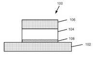
- FIG. 1is a simplified diagram illustrating a resistive switching device 100 according to an embodiment of the present invention.
- the resistive switching deviceincludes a first electrode 102 , a second electrode 106 , and a resistive switching material 104 sandwiched between the first electrode and the second electrode.
- the first electrodecan be a first conductor material.
- the first electrode 102can include a first conductive material such as a first metal material or a doped semiconductor material.
- the first metal materialcan be tungsten, aluminum, copper or other suitable metal that is compatible with CMOS fabrication techniques.
- the first electrodeis elongated in shape and extends in a first direction.
- the resistive switching material 104can include a suitable insulator material having a resistance that can be altered upon application of an electric field to the insulator material.
- the resistive switching materialcan include a silicon material.
- the silicon materialcan be an amorphous silicon material, a microcrystalline silicon material, a macro crystalline silicon material, a silicon germanium material including any combination of these materials, or the like.
- the silicon materialincludes an amorphous silicon material.
- the second electrode 106can comprise a second conductive material and can have a portion that includes a second metal material.
- the second metal materialcan be aluminum, nickel, silver, gold, palladium, platinum, or another similar metal or combination of metals.
- the second metal materialtypically is characterized by a suitable diffusivity into the resistive switching material in a specific embodiment.
- the second electrode 106is elongated in shape and extends in a second direction that is orthogonal to the first direction, as illustrated in FIG. 2 .
- the second metal materialincludes a silver material.
- the resistive switching devicefurther includes a contact material 108 disposed between the metal material of the first electrode 102 and the amorphous silicon material 104 .
- the contact materialis believed to provide a suitable interfacial defect characteristic for desirable switching behavior for the resistive switching device.
- the contact materialcan be p+ polysilicon material, p+ silicon germanium material, or the like.
- the contact materialcan be optional.
- the resistive switching devicecan be disposed in an N by M crossbar array with pillars of resistive switching material 104 located at the crossings of the array, to form a high density interconnected array of non-volatile memory cells.
- FIGS. 3-5are simplified diagrams illustrating operations of a resistive switching device.
- the second metal materialforms a metal region 302 in a portion of the resistive switching material 104 when a first positive voltage 304 greater than a threshold voltage is applied to the second electrode 106 .
- the threshold voltageis the forming voltage for the resistive switching device.
- the resistive switching deviceis at a high resistance state, otherwise known as an erase state, or an “OFF” state.
- the metal regionmay further form a filament region 402 .
- the filament region 402may be characterized by a length, a first distance between metal particles, a second distance between the filament and the first electrode 102 , and the like.
- the filamentextends in a direction 404 towards the first electrode 102 when a second positive bias voltage 406 is applied to the second electrode 106 .
- the resistive switching device 104is in a low resistance state, otherwise known as a programmed or “ON” state, allowing current to flow through the resistive switching device 104 .
- the filament structure 402retracts in a direction 502 away from first electrode 102 , when a negative bias voltage 504 or an erase voltage is applied to the second electrode 106 .
- the resistive switching device 104is reverted back to the high resistance state illustrated in FIG. 3 . Accordingly, as shown in FIGS. 3-5 .
- the resistive switching device 100is considered a two-terminal or a bipolar device.
- leakage current from un-selected cellscan form a leakage path, that affects operations of the selected cell.
- Leakage current from the selected cellcan also affect the states of unselected cells in the leakage path. As an example of this, in a situation where a selected cell is at a high conductance state, leakage current from the high conductance cell can erase an unselected cell also in the high conductance state in the leakage path.
- FIG. 6is a simplified diagram illustrating a crossbar array of memory cells 600 .
- Cell 602includes a first bottom electrode 612 , a first top electrode 614 , and a first resistive switching region 618 .
- Cell 604shares the same first bottom electrode 612 as cell 602 , and includes a second top electrode 616 and a second resistive switching region 620 .
- Cell 608shares the same first top electrode 614 as cell 602 , and includes a third bottom electrode 622 and a third resistive switching region 624 .
- Cell 610shares the same first top electrode 616 as cell 602 , and the same bottom electrode 622 as cell 608 and a fourth resistive switching region 628 .
- a positive bias voltage applied to first top electrode 614causes cell 602 to be in a low resistance state, such that an ‘ON’ state current flows in cell 602 during a subsequent read operation. If cell 604 is in a low resistance (e.g. programmed state), current leaking from cell 602 can cause cell 604 to be unintentionally erased. Similarly, if cell 602 is in a programmed state and to be erased, a negative voltage applied to first top electrode 614 can cause cell 608 to be unintentionally erased when cell 608 is in a low resistance state.
- a rectifier or a diodemay be incorporated into the design.
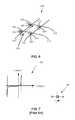
- FIG. 7illustrates a conventional diode 700 and an IV characteristic 702 of the conventional diode.
- a conventional diodelimits current flow only in one direction, the conventional diode can only reduce reverse current flow for either a program operation (e.g. positive voltage) or an erase operation (e.g. negative voltage), but typically not for both.
- the conventional diodemay experience breakdown in reversed bias or during an erase operation when a current starts to flow.
- a conventional diode configured to operate for a negative bias erase functionmay experience breakdown during a positive bias program function. After breakdown, the conventional diode becomes defective and non-functional.
- Embodiments according to the present inventionprovide a device coupled to a resistive switching device, as described above, that addresses this breakdown issue.
- the non-linear deviceis a two terminal device configured to prevent leakage current from unselected cells to interfere with proper operation of a selected cell under conditions of forward bias as well as reversed bias.
- the non-linear devicealso prevents leakage current from a selected cell during, for example programming, from unintentionally erasing one or more unselected cells or unintentionally programming one or more unselected cells.
- the non-linear deviceis serially connected to the resistive switching device and can be disposed between the first electrode ( FIG. 1 , 106 ) and the resistive switching element ( FIG.
- the non-linear devicecan be disposed between the second electrode 106 and the resistive switching element ( 104 , 108 ).
- the non-linear deviceis configured to conduct electric current when an operating voltage is applied to, for example, the second electrode 106 of the resistive switching device 100 .
- the operating voltageincludes a forward biased programming voltage and a reverse biased erase voltage in a specific embodiment.
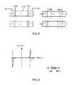
- the non-linear device 800includes a first impurity region 802 , a second impurity region 804 , and a third impurity region 806 sandwiched between the first impurity region 802 and the second impurity region 806 .
- the first impurity region 802 and the second impurity region 804have the same charge polarity characteristic and have substantially the same impurity concentration.
- the third impurity region 806has an opposite charge polarity characteristic and a lower impurity concentration than the first impurity region 802 and the second impurity region 804 .
- the non-linear devicecan have a pnp configuration or an npn configuration depending on the embodiment.
- the non-linear device 800is configured to conduct electric current when a voltage greater than a first voltage, or “punch-through” voltage, is applied.
- This type of diodemay be referred to as a punch-through diode.
- the first voltagefurther causes the resistive switching device to change from a first state (e.g. non-conductive) to a second state (e.g. conductive).
- the first statecan be an off state or a high resistance state and the second state can be a programmed state or a low resistance state.
- the first voltagecan be a programming voltage or a read voltage depending on the embodiment.
- Embodiments according to the present inventioncan be applied to a one-time programmable memory device configured in an array, for example in a crossbar array.
- the non-linear device 800includes a first depletion region 808 formed from the first impurity region 802 and the third impurity region 806 , and a second depletion region 810 formed from the second impurity region 804 and the third impurity region 806 .
- a first voltageis applied to a selected cell, (for example, in a programming operation or an erase operation)
- the first depletion region 808 and the second depletion region 810expand, as illustrated.
- the two depletion regions ( 808 and 810 )merge, so that a further increase in applied voltage would allow a current to flow and cause switching in the resistive switching device.
- the non-linear devicecan have an insulator material sandwiched between a first metal and a second metal or having a metal-insulator-metal (MIM) configuration.
- the non-linear devicecan also have a first insulator material and a second insulator material sandwiched between the first metal and the second metal or a metal-insulator-insulator-metal (M-I-I-M) configuration depending on the application.
- MIMmetal-insulator-insulator-metal
- M-I-I-Mmetal-insulator-insulator-metal
- the diode having MIM or MIIM configurationcan be disposed between the resistive switching element and the first electrode.
- the non-linear device having MIM or MIIM configurationcan be disposed between the resistive switching element and the second electrode, depending on the application.
- the present inventionhas been exemplified using silver electrode and amorphous silicon material as resistive switching material.
- the non-linear devicecan be applied to any two terminal devices to prevent leakage current from proper operation of the two terminal device. Therefore though the present invention has been described using various examples and embodiments, it is also understood that the examples and embodiments described herein are for illustrative purposes only and that various modifications or alternatives in light thereof will be suggested to persons skilled in the art and are to be included within the spirit and purview of this application and scope of the appended claims.
Landscapes
- Chemical & Material Sciences (AREA)
- Engineering & Computer Science (AREA)
- Materials Engineering (AREA)
- Semiconductor Memories (AREA)
Abstract
Description
Claims (22)
Priority Applications (3)
| Application Number | Priority Date | Filing Date | Title |
|---|---|---|---|
| US13/174,264US8659929B2 (en) | 2011-06-30 | 2011-06-30 | Amorphous silicon RRAM with non-linear device and operation |
| PCT/US2012/045312WO2013003856A2 (en) | 2011-06-30 | 2012-07-02 | Amorphous silicon rram with non-linear device and operation |
| US14/106,288US20140269001A1 (en) | 2011-06-30 | 2013-12-13 | Amorphous silicon rram with non-linear device and operation |
Applications Claiming Priority (1)
| Application Number | Priority Date | Filing Date | Title |
|---|---|---|---|
| US13/174,264US8659929B2 (en) | 2011-06-30 | 2011-06-30 | Amorphous silicon RRAM with non-linear device and operation |
Related Child Applications (1)
| Application Number | Title | Priority Date | Filing Date |
|---|---|---|---|
| US14/106,288ContinuationUS20140269001A1 (en) | 2011-06-30 | 2013-12-13 | Amorphous silicon rram with non-linear device and operation |
Publications (2)
| Publication Number | Publication Date |
|---|---|
| US20130003436A1 US20130003436A1 (en) | 2013-01-03 |
| US8659929B2true US8659929B2 (en) | 2014-02-25 |
Family
ID=47390536
Family Applications (2)
| Application Number | Title | Priority Date | Filing Date |
|---|---|---|---|
| US13/174,264Active2031-08-23US8659929B2 (en) | 2011-06-30 | 2011-06-30 | Amorphous silicon RRAM with non-linear device and operation |
| US14/106,288AbandonedUS20140269001A1 (en) | 2011-06-30 | 2013-12-13 | Amorphous silicon rram with non-linear device and operation |
Family Applications After (1)
| Application Number | Title | Priority Date | Filing Date |
|---|---|---|---|
| US14/106,288AbandonedUS20140269001A1 (en) | 2011-06-30 | 2013-12-13 | Amorphous silicon rram with non-linear device and operation |
Country Status (2)
| Country | Link |
|---|---|
| US (2) | US8659929B2 (en) |
| WO (1) | WO2013003856A2 (en) |
Cited By (5)
| Publication number | Priority date | Publication date | Assignee | Title |
|---|---|---|---|---|
| US20140269001A1 (en)* | 2011-06-30 | 2014-09-18 | Crossbar, Inc. | Amorphous silicon rram with non-linear device and operation |
| US20150302932A1 (en)* | 2012-04-27 | 2015-10-22 | Sony Corporation | Memory device, semiconductor unit and method of operating the same, and electronic apparatus |
| US9472281B1 (en) | 2015-06-30 | 2016-10-18 | HGST Netherlands B.V. | Non-volatile memory with adjustable cell bit shape |
| US9716225B2 (en) | 2014-09-03 | 2017-07-25 | Micron Technology, Inc. | Memory cells including dielectric materials, memory devices including the memory cells, and methods of forming same |
| US9728255B2 (en) | 2015-10-13 | 2017-08-08 | Western Digital Technologies, Inc. | Planar variable resistance memory |
Families Citing this family (14)
| Publication number | Priority date | Publication date | Assignee | Title |
|---|---|---|---|---|
| US10916317B2 (en)* | 2010-08-20 | 2021-02-09 | Attopsemi Technology Co., Ltd | Programmable resistance memory on thin film transistor technology |
| US10586832B2 (en) | 2011-02-14 | 2020-03-10 | Attopsemi Technology Co., Ltd | One-time programmable devices using gate-all-around structures |
| JP5364739B2 (en)* | 2011-02-18 | 2013-12-11 | 株式会社東芝 | Nonvolatile resistance change element |
| KR20140128482A (en)* | 2013-04-25 | 2014-11-06 | 에스케이하이닉스 주식회사 | Resistance Memory Device and Write Control Circuit, Memory Apparatus and Data Processing System Having the Same, and Operation Method Therefor |
| US9214228B1 (en)* | 2013-08-22 | 2015-12-15 | Kabushiki Kaisha Toshiba | Semiconductor memory device and method of forming thereof |
| WO2015072958A1 (en) | 2013-11-12 | 2015-05-21 | Hewlett-Packard Development Company, L.P. | Nonlinear memristor devices with three-layer selectors |
| KR102142648B1 (en)* | 2013-12-16 | 2020-08-10 | 삼성디스플레이 주식회사 | Photo-sensitive resin composition, method for manufacturing organic layer using the composition, and display device comprising the organic layer |
| WO2018063164A1 (en)* | 2016-09-27 | 2018-04-05 | Intel Corporation | Diode based resistive random access memory |
| US11062786B2 (en) | 2017-04-14 | 2021-07-13 | Attopsemi Technology Co., Ltd | One-time programmable memories with low power read operation and novel sensing scheme |
| US11615859B2 (en) | 2017-04-14 | 2023-03-28 | Attopsemi Technology Co., Ltd | One-time programmable memories with ultra-low power read operation and novel sensing scheme |
| TWI714862B (en) | 2017-06-19 | 2021-01-01 | 大陸商深圳瑞健生命科學硏究院有限公司 | A method and drug for regulating GLP-1/GLP-1R |
| JP2020144959A (en)* | 2019-03-06 | 2020-09-10 | キオクシア株式会社 | Semiconductor storage device |
| WO2020213968A1 (en)* | 2019-04-17 | 2020-10-22 | 삼성전자 주식회사 | Memory device |
| US11258023B1 (en)* | 2020-08-05 | 2022-02-22 | Nantero, Inc. | Resistive change elements using passivating interface gaps and methods for making same |
Citations (187)
| Publication number | Priority date | Publication date | Assignee | Title |
|---|---|---|---|---|
| US680652A (en) | 1897-11-08 | 1901-08-13 | Leonard L Elden | Circuit-breaker. |
| US4433468A (en) | 1980-03-26 | 1984-02-28 | Nippon Electric Co., Ltd. | Method for making semiconductor device having improved thermal stress characteristics |
| US4684972A (en) | 1981-08-07 | 1987-08-04 | The British Petroleum Company, P.L.C. | Non-volatile amorphous semiconductor memory device utilizing a forming voltage |
| US4741601A (en) | 1984-10-08 | 1988-05-03 | Nec Corporation | Non-linear device for driving liquid crystal display |
| US5242855A (en) | 1991-09-30 | 1993-09-07 | Nec Corporation | Method of fabricating a polycrystalline silicon film having a reduced resistivity |
| US5278085A (en) | 1992-08-11 | 1994-01-11 | Micron Semiconductor, Inc. | Single mask process for forming both n-type and p-type gates in a polycrystalline silicon layer during the formation of a semiconductor device |
| US5315131A (en) | 1990-11-22 | 1994-05-24 | Matsushita Electric Industrial Co., Ltd. | Electrically reprogrammable nonvolatile memory device |
| US5335219A (en) | 1991-01-18 | 1994-08-02 | Ovshinsky Stanford R | Homogeneous composition of microcrystalline semiconductor material, semiconductor devices and directly overwritable memory elements fabricated therefrom, and arrays fabricated from the memory elements |
| US5360981A (en) | 1989-05-11 | 1994-11-01 | British Telecommunications Public Limited Company | Amorphous silicon memory |
| US5457649A (en) | 1994-08-26 | 1995-10-10 | Microchip Technology, Inc. | Semiconductor memory device and write-once, read-only semiconductor memory array using amorphous-silicon and method therefor |
| US5538564A (en) | 1994-03-18 | 1996-07-23 | Regents Of The University Of California | Three dimensional amorphous silicon/microcrystalline silicon solar cells |
| US5541869A (en) | 1991-10-22 | 1996-07-30 | British Telecommunications, Plc | Resistive memory element |
| US5594363A (en) | 1995-04-07 | 1997-01-14 | Zycad Corporation | Logic cell and routing architecture in a field programmable gate array |
| US5614756A (en) | 1990-04-12 | 1997-03-25 | Actel Corporation | Metal-to-metal antifuse with conductive |
| US5627451A (en) | 1993-04-28 | 1997-05-06 | Fujitsu Limited | Control method and control apparatus for secondary battery charging in constant current charging method |
| US5751012A (en) | 1995-06-07 | 1998-05-12 | Micron Technology, Inc. | Polysilicon pillar diode for use in a non-volatile memory cell |
| US5840608A (en) | 1996-11-22 | 1998-11-24 | United Microelectronics Corporation | High density ROM and a method of making the same |
| US5970332A (en) | 1995-03-28 | 1999-10-19 | U.S. Philips Corporation | Method of manufacturing a semiconductor device with a BiCMOS circuit |
| US5998244A (en) | 1996-08-22 | 1999-12-07 | Micron Technology, Inc. | Memory cell incorporating a chalcogenide element and method of making same |
| US6128214A (en) | 1999-03-29 | 2000-10-03 | Hewlett-Packard | Molecular wire crossbar memory |
| US6143642A (en) | 1997-12-22 | 2000-11-07 | Vlsi Technology, Inc. | Programmable semiconductor structures and methods for making the same |
| US6259116B1 (en) | 1997-10-22 | 2001-07-10 | U.S. Philips Corporation | Multiple memory element semiconductor memory devices |
| US6291836B1 (en) | 1996-06-05 | 2001-09-18 | U. S. Philips Corporation | Method of operating a programmable, non-volatile memory device |
| US6436818B1 (en) | 1997-02-19 | 2002-08-20 | Micron Technology, Inc. | Semiconductor structure having a doped conductive layer |
| US6436765B1 (en) | 2001-02-09 | 2002-08-20 | United Microelectronics Corp. | Method of fabricating a trenched flash memory cell |
| US6492694B2 (en) | 1998-02-27 | 2002-12-10 | Micron Technology, Inc. | Highly conductive composite polysilicon gate for CMOS integrated circuits |
| US20040026682A1 (en) | 2002-06-17 | 2004-02-12 | Hai Jiang | Nano-dot memory and fabricating same |
| US6762474B1 (en) | 1998-06-10 | 2004-07-13 | Agere Systems Inc. | Method and apparatus for temperature compensation of read-only memory |
| US6768157B2 (en) | 2001-08-13 | 2004-07-27 | Advanced Micro Devices, Inc. | Memory device |
| US20040170040A1 (en) | 2002-08-02 | 2004-09-02 | Unity Semiconductor Corporation | Rewritable memory with non-linear memory element |
| US6815286B2 (en) | 2001-08-13 | 2004-11-09 | Advanced Micro Devices, Inc. | Memory device |
| US6838720B2 (en) | 2001-08-13 | 2005-01-04 | Advanced Micro Devices, Inc. | Memory device with active passive layers |
| US20050020510A1 (en) | 2002-08-29 | 2005-01-27 | Benedict Dale L. | D-mannose contraceptives |
| US20050029587A1 (en) | 1995-06-07 | 2005-02-10 | Harshfield Steven T. | Method and apparatus for forming an integrated circuit electrode having a reduced contact area |
| US6858481B2 (en) | 2001-08-13 | 2005-02-22 | Advanced Micro Devices, Inc. | Memory device with active and passive layers |
| US6858482B2 (en) | 2002-04-10 | 2005-02-22 | Micron Technology, Inc. | Method of manufacture of programmable switching circuits and memory cells employing a glass layer |
| US6864127B2 (en) | 1997-04-25 | 2005-03-08 | Semiconductor Energy Laboratory Co., Ltd. | Semiconductor device and method of fabricating the same |
| US20050062045A1 (en) | 2002-10-02 | 2005-03-24 | Arup Bhattacharyya | Processes of forming stacked resistor constructions |
| US6927430B2 (en) | 2001-06-28 | 2005-08-09 | Sharp Laboratories Of America, Inc. | Shared bit line cross-point memory array incorporating P/N junctions |
| US6939787B2 (en) | 1999-12-28 | 2005-09-06 | Fujitsu Limited | Method for fabricating semiconductor device having gate electrode with polymetal structure of polycrystalline silicon film and metal film |
| US6946719B2 (en) | 2003-12-03 | 2005-09-20 | Matrix Semiconductor, Inc | Semiconductor device including junction diode contacting contact-antifuse unit comprising silicide |
| US7020006B2 (en) | 2002-08-02 | 2006-03-28 | Unity Semiconductor Corporation | Discharge of conductive array lines in fast memory |
| US7023093B2 (en) | 2002-10-24 | 2006-04-04 | International Business Machines Corporation | Very low effective dielectric constant interconnect Structures and methods for fabricating the same |
| US7102150B2 (en) | 2001-05-11 | 2006-09-05 | Harshfield Steven T | PCRAM memory cell and method of making same |
| US7122853B1 (en) | 2004-08-17 | 2006-10-17 | Fasl, Inc. | Method to improve yield and simplify operation of polymer memory cells |
| US20060281244A1 (en) | 2005-06-08 | 2006-12-14 | Masayuki Ichige | Nonvolatile semiconductor memory device and method of manufacturing the same |
| US20060286762A1 (en) | 2005-06-15 | 2006-12-21 | Winbond Electronics Corp. | Method for non-volatile memory fabrication |
| US20070008773A1 (en) | 2005-07-11 | 2007-01-11 | Matrix Semiconductor, Inc. | Nonvolatile memory cell comprising switchable resistor and transistor |
| US20070015348A1 (en) | 2005-07-18 | 2007-01-18 | Sharp Laboratories Of America, Inc. | Crosspoint resistor memory device with back-to-back Schottky diodes |
| US7187577B1 (en) | 2005-11-23 | 2007-03-06 | Grandis, Inc. | Method and system for providing current balanced writing for memory cells and magnetic devices |
| US20070069119A1 (en) | 2005-09-23 | 2007-03-29 | Massachusetts Institute Of Technology | Optical trapping with a semiconductor |
| US20070087508A1 (en) | 2003-12-03 | 2007-04-19 | Herner S B | Method for making a p-i-n diode crystallized adjacent to a silicide in series with a dielectric antifuse |
| US20070090425A1 (en) | 2005-09-28 | 2007-04-26 | Matrix Semiconductor, Inc. | Memory cell comprising switchable semiconductor memory element with trimmable resistance |
| US20070105390A1 (en) | 2005-11-09 | 2007-05-10 | Oh Travis B | Oxygen depleted etching process |
| US20070105284A1 (en) | 2003-12-03 | 2007-05-10 | Herner S B | Method for forming a memory cell comprising a semiconductor junction diode crystallized adjacent to a silicide |
| US7221599B1 (en) | 2004-11-01 | 2007-05-22 | Spansion, Llc | Polymer memory cell operation |
| US7238607B2 (en) | 2002-12-19 | 2007-07-03 | Sandisk 3D Llc | Method to minimize formation of recess at surface planarized by chemical mechanical planarization |
| US20070171698A1 (en) | 2005-12-23 | 2007-07-26 | Heinz Hoenigschmid | Memory circuit including a resistive memory element and method for operating such a memory circuit |
| US20070205510A1 (en) | 2006-03-03 | 2007-09-06 | Lavoie Adrien R | Noble metal barrier layers |
| US20070228414A1 (en) | 2006-03-31 | 2007-10-04 | Sandisk 3D, Llc | Heterojunction device comprising a semiconductor and a resistivity-switching oxide or nitride |
| US7289353B2 (en) | 2004-08-17 | 2007-10-30 | Spansion, Llc | Systems and methods for adjusting programming thresholds of polymer memory cells |
| US20070284575A1 (en) | 2005-07-18 | 2007-12-13 | Sharp Laboratories Of America, Inc. | Metal/semiconductor/metal current limiter |
| US20070290186A1 (en) | 2006-05-04 | 2007-12-20 | El Mostafa Bourim | Non-volatile variable resistance memory device and method of fabricating the same |
| US20080002481A1 (en) | 2002-12-20 | 2008-01-03 | Dietmar Gogl | Integrated Circuit, Method of Operating an Integrated Circuit, Method of Manufacturing an Integrated Circuit, Memory Module, Stackable Memory Module |
| US20080006907A1 (en) | 2006-07-06 | 2008-01-10 | Samsung Electronics Co., Ltd | Non-volatile memory device including a variable resistance material |
| US20080019163A1 (en) | 2006-07-21 | 2008-01-24 | Heinz Hoenigschmid | Method and memory circuit for operating a resistive memory cell |
| US7324363B2 (en) | 2005-12-12 | 2008-01-29 | Synopsys, Inc. | SPICE optimized for arrays |
| US20080048164A1 (en) | 2006-07-11 | 2008-02-28 | Matsushita Electric Industrial Co., Ltd. | Electro-resistance element, method of manufacturing the same and electro-resistance memory using the same |
| US20080089110A1 (en) | 2006-10-16 | 2008-04-17 | Warren Robinett | Crossbar-memory systems and methods for writing to and reading from crossbar memory junctions of crossbar-memory systems |
| US20080090337A1 (en) | 2006-10-03 | 2008-04-17 | Williams R Stanley | Electrically actuated switch |
| US7365411B2 (en) | 2004-08-12 | 2008-04-29 | Micron Technology, Inc. | Resistance variable memory with temperature tolerant materials |
| US20080106926A1 (en) | 2006-11-08 | 2008-05-08 | Symetrix Corporation | Non-volatile resistance switching memories and methods of making same |
| US20080106925A1 (en) | 2006-11-08 | 2008-05-08 | Symetrix Corporation | Correlated electron memory |
| US20080165571A1 (en) | 2007-01-09 | 2008-07-10 | Macronix International Co., Ltd. | Method, Apparatus and Computer Program Product for Read Before Programming Process on Multiple Programmable Resistive Memory Cell |
| US7405418B2 (en) | 2004-02-17 | 2008-07-29 | Infineon Technologies Ag | Memory device electrode with a surface structure |
| US20080185567A1 (en) | 2007-02-05 | 2008-08-07 | Nitin Kumar | Methods for forming resistive switching memory elements |
| US20080206931A1 (en) | 2002-07-26 | 2008-08-28 | Laurent Breuil | Nonvolatile memory element and production method thereof and storage memory arrangement |
| US20080278988A1 (en) | 2007-05-09 | 2008-11-13 | Klaus Ufert | Resistive switching element |
| US20080278990A1 (en) | 2007-05-09 | 2008-11-13 | Pragati Kumar | Resistive-switching nonvolatile memory elements |
| US20080301497A1 (en) | 2007-06-04 | 2008-12-04 | Silicon Motion, Inc. | Testing Apparatus, System, and Method for Testing at Least One Device with a Connection Interface |
| US20080304312A1 (en) | 2007-06-11 | 2008-12-11 | Macronix International Co., Ltd. | Resistance memory with tungsten compound and manufacturing |
| US20080311722A1 (en) | 2007-06-15 | 2008-12-18 | Sandisk 3D Llc | Method for forming polycrystalline thin film bipolar transistors |
| US20090001345A1 (en) | 2007-06-29 | 2009-01-01 | April Schricker | Memory cell that employs a selectively deposited reversible resistance-switching element and methods of forming the same |
| US7474000B2 (en) | 2003-12-05 | 2009-01-06 | Sandisk 3D Llc | High density contact to relaxed geometry layers |
| WO2009005699A1 (en) | 2007-06-29 | 2009-01-08 | Sandisk 3D, Llc | Memory cell that employs a selectively grown reversible resistance-switching element and methods of forming the same |
| US20090014707A1 (en) | 2006-10-20 | 2009-01-15 | Wei Lu | Non-volatile solid state resistive switching devices |
| US20090052226A1 (en) | 2007-08-24 | 2009-02-26 | Samsung Electronics Co., Ltd | Resistive random access memory device |
| US20090095951A1 (en) | 2007-10-12 | 2009-04-16 | Ovonyx, Inc. | Memory Device With Low Reset Current |
| US7521705B2 (en) | 2005-08-15 | 2009-04-21 | Micron Technology, Inc. | Reproducible resistance variable insulating memory devices having a shaped bottom electrode |
| US7534625B2 (en) | 2004-09-24 | 2009-05-19 | Karpov Ilya V | Phase change memory with damascene memory element |
| US20090152737A1 (en) | 2000-07-14 | 2009-06-18 | Micron Technology, Inc. | Memory devices having contact features |
| US7550380B2 (en) | 2004-11-03 | 2009-06-23 | Micron Technology, Inc. | Electroless plating of metal caps for chalcogenide-based memory devices |
| US20090168486A1 (en) | 2007-12-27 | 2009-07-02 | Sandisk 3D Llc | Large capacity one-time programmable memory cell using metal oxides |
| US20090231910A1 (en) | 2008-03-11 | 2009-09-17 | Micron Technology, Inc. | Non-volatile memory with resistive access component |
| US20090250787A1 (en) | 2008-04-07 | 2009-10-08 | Toshie Kutsunai | Semiconductor storage device and manufacturing method of the same |
| US20090256130A1 (en) | 2008-04-11 | 2009-10-15 | Sandisk 3D Llc | Memory cell that employs a selectively fabricated carbon nano-tube reversible resistance-switching element, and methods of forming the same |
| US20090257265A1 (en)* | 2008-04-11 | 2009-10-15 | Sandisk 3D Llc | Multilevel nonvolatile memory device containing a carbon storage material and methods of making and using same |
| US7606059B2 (en) | 2003-03-18 | 2009-10-20 | Kabushiki Kaisha Toshiba | Three-dimensional programmable resistance memory device with a read/write circuit stacked under a memory cell array |
| US7615439B1 (en) | 2008-09-29 | 2009-11-10 | Sandisk Corporation | Damascene process for carbon memory element with MIIM diode |
| US20090298224A1 (en) | 2002-12-13 | 2009-12-03 | Lowrey Tyler A | Memory and Access Device and Method Therefor |
| US20090321706A1 (en) | 2008-06-25 | 2009-12-31 | Qimonda Ag | Resistive Memory Devices with Improved Resistive Changing Elements |
| US20090321789A1 (en) | 2008-06-30 | 2009-12-31 | Sandisk 3D Llc | Triangle two dimensional complementary patterning of pillars |
| US20100012914A1 (en) | 2008-07-18 | 2010-01-21 | Sandisk 3D Llc | Carbon-based resistivity-switching materials and methods of forming the same |
| US20100019221A1 (en) | 2008-07-22 | 2010-01-28 | Macronix International Co., Ltd. | Fully self-aligned pore-type memory cell having diode access device |
| US20100019310A1 (en) | 2008-07-25 | 2010-01-28 | Kabushiki Kaisha Toshiba | Semiconductor memory device |
| US20100032638A1 (en) | 2008-08-07 | 2010-02-11 | Sandisk 3D Llc | Memory cell that includes a carbon-based memory element and methods of forming the same |
| US7667442B2 (en) | 2005-03-16 | 2010-02-23 | Ricoh Company, Ltd. | Constant voltage power supply circuit and method of testing the same |
| US20100084625A1 (en) | 2008-10-02 | 2010-04-08 | Guy Wicker | Memory Device |
| US20100085798A1 (en) | 2008-10-08 | 2010-04-08 | The Regents Of The University Of Michigan | Silicon-based nanoscale resistive device with adjustable resistance |
| US20100090192A1 (en) | 2006-08-31 | 2010-04-15 | Nxp, B.V. | Method for controlled formation of the resistive switching material in a resistive switching device and device obtained thereof |
| US7704788B2 (en) | 2007-04-06 | 2010-04-27 | Samsung Electronics Co., Ltd. | Methods of fabricating multi-bit phase-change memory devices and devices formed thereby |
| US20100101290A1 (en) | 2008-10-24 | 2010-04-29 | Antonio Bertolotto | Method for the production of an agent for treatment of agricultural soils |
| US20100102290A1 (en) | 2008-10-20 | 2010-04-29 | The Regents Of The University Of Michigan | Silicon based nanoscale crossbar memory |
| US7729158B2 (en) | 2003-04-03 | 2010-06-01 | Kabushiki Kaisha Toshiba | Resistance change memory device |
| US7728318B2 (en) | 2006-11-16 | 2010-06-01 | Sandisk Corporation | Nonvolatile phase change memory cell having a reduced contact area |
| US20100157710A1 (en) | 2008-12-19 | 2010-06-24 | Unity Semiconductor Corporation | Array Operation Using A Schottky Diode As a Non-Ohmic Isolation Device |
| US20100157651A1 (en)* | 2008-12-18 | 2010-06-24 | Sandisk 3D Llc | Method of programming a nonvolatile memory device containing a carbon storage material |
| US20100163828A1 (en) | 2008-12-30 | 2010-07-01 | Industrial Technology Research Institute | Phase change memory devices and methods for fabricating the same |
| US7749805B2 (en) | 2005-03-10 | 2010-07-06 | Qimonda Ag | Method for manufacturing an integrated circuit including an electrolyte material layer |
| US20100176368A1 (en) | 2009-01-14 | 2010-07-15 | Ko Nikka | Method of manufacturing semiconductor memory device, and semiconductor memory device |
| US7772581B2 (en) | 2006-09-11 | 2010-08-10 | Macronix International Co., Ltd. | Memory device having wide area phase change element and small electrode contact area |
| US7786589B2 (en) | 2006-12-06 | 2010-08-31 | Kabushiki Kaisha Toshiba | Semiconductor device and method for manufacturing semiconductor device |
| US7786464B2 (en) | 2007-11-20 | 2010-08-31 | Infineon Technologies Ag | Integrated circuit having dielectric layer including nanocrystals |
| US20100219510A1 (en) | 2008-06-30 | 2010-09-02 | Sandisk 3D Llc | Method for fabricating high density pillar structures by double patterning using positive photoresist |
| US20100221868A1 (en) | 2007-12-04 | 2010-09-02 | Regino Sandoval | Active Material Devices with Containment Layer |
| US20100237314A1 (en) | 2009-03-19 | 2010-09-23 | Takayuki Tsukamoto | Resistance change type memory |
| US7824956B2 (en) | 2007-06-29 | 2010-11-02 | Sandisk 3D Llc | Memory cell that employs a selectively grown reversible resistance-switching element and methods of forming the same |
| US20100277969A1 (en) | 2008-10-31 | 2010-11-04 | Seagate Technology Llc. | Structures for resistive random access memory cells |
| US7829875B2 (en) | 2006-03-31 | 2010-11-09 | Sandisk 3D Llc | Nonvolatile rewritable memory cell comprising a resistivity-switching oxide or nitride and an antifuse |
| US7835170B2 (en) | 2005-05-09 | 2010-11-16 | Nantero, Inc. | Memory elements and cross point switches and arrays of same using nonvolatile nanotube blocks |
| US20100321095A1 (en) | 2008-06-10 | 2010-12-23 | Takumi Mikawa | Semiconductor device, manufacturing method of semiconductor device, semiconductor chip and system |
| US7859884B2 (en) | 2005-01-19 | 2010-12-28 | Sandisk 3D Llc | Structure and method for biasing phase change memory array for reliable writing |
| US7881097B2 (en) | 2006-12-26 | 2011-02-01 | Sony Corporation | Storage element and memory |
| US7897953B2 (en) | 2008-01-16 | 2011-03-01 | Micron Technology, Inc. | Multi-level programmable PCRAM memory |
| US7898838B2 (en) | 2008-10-31 | 2011-03-01 | Seagate Technology Llc | Resistive sense memory calibration for self-reference read method |
| US7920412B2 (en) | 2006-09-29 | 2011-04-05 | Kabushiki Kaisha Toshiba | Magnetic random access memory and method of manufacturing the same |
| US7924138B2 (en) | 2007-03-01 | 2011-04-12 | Fujitsu Limited | Semiconductor device and manufacturing method of the same |
| US20110089391A1 (en) | 2009-10-20 | 2011-04-21 | Andrei Mihnea | Punch-through diode steering element |
| US20110136327A1 (en) | 2009-12-03 | 2011-06-09 | Applied Materials, Inc. | High mobility monolithic p-i-n diodes |
| US20110133149A1 (en) | 2009-12-04 | 2011-06-09 | Sonehara Takeshi | Resistance change memory and manufacturing method thereof |
| US7968419B2 (en) | 2005-07-18 | 2011-06-28 | Sharp Laboratories Of America, Inc. | Back-to-back metal/semiconductor/metal (MSM) Schottky diode |
| US20110155991A1 (en) | 2009-12-29 | 2011-06-30 | Industrial Technology Research Institute | Resistive memory device and fabricating method thereof |
| US7984776B2 (en) | 2007-03-30 | 2011-07-26 | The Regents Of The University Of Michigan | Energy storage and control system for a vehicle electrified drivetrain |
| US20110198557A1 (en) | 2008-02-07 | 2011-08-18 | International Business Machines Corporation | Method for fabrication of crystalline diodes for resistive memories |
| US8004882B2 (en) | 2004-06-04 | 2011-08-23 | Micron Technology, Inc. | Spintronic devices with integrated transistors |
| US20110204312A1 (en) | 2008-05-10 | 2011-08-25 | Intermolecular, Inc. | Confinement techniques for non-volatile resistive-switching memories |
| US20110204314A1 (en) | 2005-03-28 | 2011-08-25 | Samsung Electronics Co., Ltd. | Resistive memory cells and devices having asymmetrical contacts |
| US20110205782A1 (en) | 2010-02-23 | 2011-08-25 | Xiying Chen Costa | Step soft program for reversible resistivity-switching elements |
| US20110212616A1 (en) | 2010-02-26 | 2011-09-01 | Robert Seidel | Metallization system of a semiconductor device comprising rounded interconnects formed by hard mask rounding |
| US8018760B2 (en) | 2006-12-28 | 2011-09-13 | Panasonic Corporation | Resistance variable element and resistance variable memory apparatus |
| US20110227028A1 (en) | 2010-03-16 | 2011-09-22 | Deepak Chandra Sekar | Bottom electrodes for use with metal oxide resistivity switching layers |
| US8045364B2 (en) | 2009-12-18 | 2011-10-25 | Unity Semiconductor Corporation | Non-volatile memory device ion barrier |
| US8054674B2 (en) | 2007-05-10 | 2011-11-08 | Sharp Kabushiki Kaisha | Variable resistive element, manufacturing method for same, and non-volatile semiconductor memory device |
| US20110284814A1 (en) | 2010-05-24 | 2011-11-24 | Guobiao Zhang | Large Bit-Per-Cell Three-Dimensional Mask-Programmable Read-Only Memory |
| US8067815B2 (en) | 2008-12-11 | 2011-11-29 | Macronix International Co., Lt.d. | Aluminum copper oxide based memory devices and methods for manufacture |
| US20110305064A1 (en) | 2010-06-11 | 2011-12-15 | Crossbar, Inc. | Interface control for improved switching in rram |
| US20110310656A1 (en) | 2010-06-18 | 2011-12-22 | Franz Kreupl | Memory Cell With Resistance-Switching Layers Including Breakdown Layer |
| US20110317470A1 (en) | 2010-06-24 | 2011-12-29 | The Regents Of The University Of Michigan | Rectification element and method for resistive switching for non volatile memory device |
| US8088688B1 (en) | 2010-11-05 | 2012-01-03 | Crossbar, Inc. | p+ polysilicon material on aluminum for non-volatile memory device and method |
| EP2405441A1 (en) | 2010-07-09 | 2012-01-11 | Crossbar, Inc. | Resistive memory using SiGe material |
| US20120007035A1 (en) | 2010-07-12 | 2012-01-12 | Crossbar, Inc. | Intrinsic Programming Current Control for a RRAM |
| US8097874B2 (en) | 2008-10-30 | 2012-01-17 | Seagate Technology Llc | Programmable resistive memory cell with sacrificial metal |
| EP2408035A2 (en) | 2010-07-13 | 2012-01-18 | Crossbar, Inc. | Two terminal resistive switching device structure and method of fabricating |
| US20120012806A1 (en) | 2010-07-13 | 2012-01-19 | Crossbar, Inc. | Improved on/off ratio for non-volatile memory device and method |
| US20120025161A1 (en) | 2008-02-27 | 2012-02-02 | Manuj Rathor | Diode and resistive memory device structures |
| US20120033479A1 (en) | 2010-08-06 | 2012-02-09 | Lsi Corporation | Modification of logic by morphological manipulation of a semiconductor resistive element |
| US20120043519A1 (en) | 2010-08-23 | 2012-02-23 | Crossbar, Inc. | Device switching using layered device structure |
| US20120043654A1 (en) | 2010-08-19 | 2012-02-23 | Taiwan Semiconductor Manufacturing Company, Ltd. | Mechanisms for forming copper pillar bumps using patterned anodes |
| US8143092B2 (en) | 2008-03-10 | 2012-03-27 | Pragati Kumar | Methods for forming resistive switching memory elements by heating deposited layers |
| US20120108030A1 (en) | 2010-10-27 | 2012-05-03 | Crossbar, Inc. | Method for obtaining smooth, continuous silver film |
| US20120104351A1 (en) | 2010-07-01 | 2012-05-03 | Zhiqiang Wei | Non-volatile memory cell, non-volatile memory cell array, and method of manufacturing the same |
| US8183553B2 (en) | 2009-04-10 | 2012-05-22 | Intermolecular, Inc. | Resistive switching memory element including doped silicon electrode |
| US8198144B2 (en) | 2010-06-11 | 2012-06-12 | Crossbar, Inc. | Pillar structure for memory device and method |
| US20120145984A1 (en) | 2010-12-13 | 2012-06-14 | Peter Rabkin | Punch-through diode |
| US20120155146A1 (en) | 2010-12-20 | 2012-06-21 | Yoshihiro Ueda | Resistance-change memory |
| US8207064B2 (en) | 2009-09-17 | 2012-06-26 | Sandisk 3D Llc | 3D polysilicon diode with low contact resistance and method for forming same |
| US8233308B2 (en) | 2007-06-29 | 2012-07-31 | Sandisk 3D Llc | Memory cell that employs a selectively deposited reversible resistance-switching element and methods of forming the same |
| US8231998B2 (en) | 2007-03-30 | 2012-07-31 | The Regents Of The University Of Michigan | Deposited microarchitectured battery and manufacturing method |
| US8237146B2 (en)* | 2010-02-24 | 2012-08-07 | Sandisk 3D Llc | Memory cell with silicon-containing carbon switching layer and methods for forming the same |
| US20120205606A1 (en) | 2011-02-14 | 2012-08-16 | Dongguk University Industry-Academic Cooperation Foundation | Nonvolatile Memory Device Using The Resistive Switching of Graphene Oxide And The Fabrication Method Thereof |
| US8258020B2 (en) | 2010-11-04 | 2012-09-04 | Crossbar Inc. | Interconnects for stacked non-volatile memory device and method |
| US20120235112A1 (en) | 2010-11-30 | 2012-09-20 | Huo Zongliang | Resistive switching memory and method for manufacturing the same |
| US8274812B2 (en) | 2010-06-14 | 2012-09-25 | Crossbar, Inc. | Write and erase scheme for resistive memory device |
| US8315079B2 (en) | 2010-10-07 | 2012-11-20 | Crossbar, Inc. | Circuit for concurrent read operation and method therefor |
| US8320160B2 (en) | 2011-03-18 | 2012-11-27 | Crossbar, Inc. | NAND architecture having a resistive memory cell connected to a control gate of a field-effect transistor |
| US8385100B2 (en) | 2009-12-08 | 2013-02-26 | Intel Corporation | Energy-efficient set write of phase change memory with switch |
| US8394670B2 (en) | 2011-05-31 | 2013-03-12 | Crossbar, Inc. | Vertical diodes for non-volatile memory device |
Family Cites Families (5)
| Publication number | Priority date | Publication date | Assignee | Title |
|---|---|---|---|---|
| JP5475776B2 (en)* | 2008-07-31 | 2014-04-16 | ヒューレット−パッカード デベロップメント カンパニー エル.ピー. | Multilayer reconfigurable switch |
| US7969011B2 (en)* | 2008-09-29 | 2011-06-28 | Sandisk 3D Llc | MIIM diodes having stacked structure |
| US8455855B2 (en)* | 2009-01-12 | 2013-06-04 | Micron Technology, Inc. | Memory cell having dielectric memory element |
| US8450711B2 (en)* | 2009-01-26 | 2013-05-28 | Hewlett-Packard Development Company, L.P. | Semiconductor memristor devices |
| US8659929B2 (en)* | 2011-06-30 | 2014-02-25 | Crossbar, Inc. | Amorphous silicon RRAM with non-linear device and operation |
- 2011
- 2011-06-30USUS13/174,264patent/US8659929B2/enactiveActive
- 2012
- 2012-07-02WOPCT/US2012/045312patent/WO2013003856A2/enactiveApplication Filing
- 2013
- 2013-12-13USUS14/106,288patent/US20140269001A1/ennot_activeAbandoned
Patent Citations (208)
| Publication number | Priority date | Publication date | Assignee | Title |
|---|---|---|---|---|
| US680652A (en) | 1897-11-08 | 1901-08-13 | Leonard L Elden | Circuit-breaker. |
| US4433468A (en) | 1980-03-26 | 1984-02-28 | Nippon Electric Co., Ltd. | Method for making semiconductor device having improved thermal stress characteristics |
| US4684972A (en) | 1981-08-07 | 1987-08-04 | The British Petroleum Company, P.L.C. | Non-volatile amorphous semiconductor memory device utilizing a forming voltage |
| US4741601A (en) | 1984-10-08 | 1988-05-03 | Nec Corporation | Non-linear device for driving liquid crystal display |
| US5360981A (en) | 1989-05-11 | 1994-11-01 | British Telecommunications Public Limited Company | Amorphous silicon memory |
| US5614756A (en) | 1990-04-12 | 1997-03-25 | Actel Corporation | Metal-to-metal antifuse with conductive |
| US5315131A (en) | 1990-11-22 | 1994-05-24 | Matsushita Electric Industrial Co., Ltd. | Electrically reprogrammable nonvolatile memory device |
| US5335219A (en) | 1991-01-18 | 1994-08-02 | Ovshinsky Stanford R | Homogeneous composition of microcrystalline semiconductor material, semiconductor devices and directly overwritable memory elements fabricated therefrom, and arrays fabricated from the memory elements |
| US5242855A (en) | 1991-09-30 | 1993-09-07 | Nec Corporation | Method of fabricating a polycrystalline silicon film having a reduced resistivity |
| US5541869A (en) | 1991-10-22 | 1996-07-30 | British Telecommunications, Plc | Resistive memory element |
| US5278085A (en) | 1992-08-11 | 1994-01-11 | Micron Semiconductor, Inc. | Single mask process for forming both n-type and p-type gates in a polycrystalline silicon layer during the formation of a semiconductor device |
| US5627451A (en) | 1993-04-28 | 1997-05-06 | Fujitsu Limited | Control method and control apparatus for secondary battery charging in constant current charging method |
| US5538564A (en) | 1994-03-18 | 1996-07-23 | Regents Of The University Of California | Three dimensional amorphous silicon/microcrystalline silicon solar cells |
| US5457649A (en) | 1994-08-26 | 1995-10-10 | Microchip Technology, Inc. | Semiconductor memory device and write-once, read-only semiconductor memory array using amorphous-silicon and method therefor |
| US5714416A (en) | 1994-08-26 | 1998-02-03 | Microchip Technology Incorporated | Semiconductor memory device and write-once, read-only semiconductor memory array using amorphous-silicon and method therefor |
| US5970332A (en) | 1995-03-28 | 1999-10-19 | U.S. Philips Corporation | Method of manufacturing a semiconductor device with a BiCMOS circuit |
| US5594363A (en) | 1995-04-07 | 1997-01-14 | Zycad Corporation | Logic cell and routing architecture in a field programmable gate array |
| US5751012A (en) | 1995-06-07 | 1998-05-12 | Micron Technology, Inc. | Polysilicon pillar diode for use in a non-volatile memory cell |
| US20050029587A1 (en) | 1995-06-07 | 2005-02-10 | Harshfield Steven T. | Method and apparatus for forming an integrated circuit electrode having a reduced contact area |
| US6291836B1 (en) | 1996-06-05 | 2001-09-18 | U. S. Philips Corporation | Method of operating a programmable, non-volatile memory device |
| US5998244A (en) | 1996-08-22 | 1999-12-07 | Micron Technology, Inc. | Memory cell incorporating a chalcogenide element and method of making same |
| US5840608A (en) | 1996-11-22 | 1998-11-24 | United Microelectronics Corporation | High density ROM and a method of making the same |
| US6436818B1 (en) | 1997-02-19 | 2002-08-20 | Micron Technology, Inc. | Semiconductor structure having a doped conductive layer |
| US6864127B2 (en) | 1997-04-25 | 2005-03-08 | Semiconductor Energy Laboratory Co., Ltd. | Semiconductor device and method of fabricating the same |
| US6259116B1 (en) | 1997-10-22 | 2001-07-10 | U.S. Philips Corporation | Multiple memory element semiconductor memory devices |
| US6143642A (en) | 1997-12-22 | 2000-11-07 | Vlsi Technology, Inc. | Programmable semiconductor structures and methods for making the same |
| US6492694B2 (en) | 1998-02-27 | 2002-12-10 | Micron Technology, Inc. | Highly conductive composite polysilicon gate for CMOS integrated circuits |
| US6762474B1 (en) | 1998-06-10 | 2004-07-13 | Agere Systems Inc. | Method and apparatus for temperature compensation of read-only memory |
| US6128214A (en) | 1999-03-29 | 2000-10-03 | Hewlett-Packard | Molecular wire crossbar memory |
| US6939787B2 (en) | 1999-12-28 | 2005-09-06 | Fujitsu Limited | Method for fabricating semiconductor device having gate electrode with polymetal structure of polycrystalline silicon film and metal film |
| US20090152737A1 (en) | 2000-07-14 | 2009-06-18 | Micron Technology, Inc. | Memory devices having contact features |
| US20120080798A1 (en) | 2000-07-14 | 2012-04-05 | Round Rock Research, Llc | Memory devices having contact features |
| US6436765B1 (en) | 2001-02-09 | 2002-08-20 | United Microelectronics Corp. | Method of fabricating a trenched flash memory cell |
| US7102150B2 (en) | 2001-05-11 | 2006-09-05 | Harshfield Steven T | PCRAM memory cell and method of making same |
| US6927430B2 (en) | 2001-06-28 | 2005-08-09 | Sharp Laboratories Of America, Inc. | Shared bit line cross-point memory array incorporating P/N junctions |
| US7026702B2 (en) | 2001-08-13 | 2006-04-11 | Advanced Micro Devices, Inc. | Memory device |
| US6838720B2 (en) | 2001-08-13 | 2005-01-04 | Advanced Micro Devices, Inc. | Memory device with active passive layers |
| US6858481B2 (en) | 2001-08-13 | 2005-02-22 | Advanced Micro Devices, Inc. | Memory device with active and passive layers |
| US6815286B2 (en) | 2001-08-13 | 2004-11-09 | Advanced Micro Devices, Inc. | Memory device |
| US6864522B2 (en) | 2001-08-13 | 2005-03-08 | Advanced Micro Devices, Inc. | Memory device |
| US7254053B2 (en) | 2001-08-13 | 2007-08-07 | Advanced Micro Devices, Inc. | Active programming and operation of a memory device |
| US6768157B2 (en) | 2001-08-13 | 2004-07-27 | Advanced Micro Devices, Inc. | Memory device |
| US6858482B2 (en) | 2002-04-10 | 2005-02-22 | Micron Technology, Inc. | Method of manufacture of programmable switching circuits and memory cells employing a glass layer |
| US7479650B2 (en) | 2002-04-10 | 2009-01-20 | Micron Technology, Inc. | Method of manufacture of programmable conductor memory |
| US20040026682A1 (en) | 2002-06-17 | 2004-02-12 | Hai Jiang | Nano-dot memory and fabricating same |
| US20080206931A1 (en) | 2002-07-26 | 2008-08-28 | Laurent Breuil | Nonvolatile memory element and production method thereof and storage memory arrangement |
| US7020006B2 (en) | 2002-08-02 | 2006-03-28 | Unity Semiconductor Corporation | Discharge of conductive array lines in fast memory |
| US20040170040A1 (en) | 2002-08-02 | 2004-09-02 | Unity Semiconductor Corporation | Rewritable memory with non-linear memory element |
| US20050020510A1 (en) | 2002-08-29 | 2005-01-27 | Benedict Dale L. | D-mannose contraceptives |
| US20050062045A1 (en) | 2002-10-02 | 2005-03-24 | Arup Bhattacharyya | Processes of forming stacked resistor constructions |
| US7023093B2 (en) | 2002-10-24 | 2006-04-04 | International Business Machines Corporation | Very low effective dielectric constant interconnect Structures and methods for fabricating the same |
| US20090298224A1 (en) | 2002-12-13 | 2009-12-03 | Lowrey Tyler A | Memory and Access Device and Method Therefor |
| US7238607B2 (en) | 2002-12-19 | 2007-07-03 | Sandisk 3D Llc | Method to minimize formation of recess at surface planarized by chemical mechanical planarization |
| US7433253B2 (en) | 2002-12-20 | 2008-10-07 | Qimonda Ag | Integrated circuit, method of operating an integrated circuit, method of manufacturing an integrated circuit, memory module, stackable memory module |
| US20080002481A1 (en) | 2002-12-20 | 2008-01-03 | Dietmar Gogl | Integrated Circuit, Method of Operating an Integrated Circuit, Method of Manufacturing an Integrated Circuit, Memory Module, Stackable Memory Module |
| US7606059B2 (en) | 2003-03-18 | 2009-10-20 | Kabushiki Kaisha Toshiba | Three-dimensional programmable resistance memory device with a read/write circuit stacked under a memory cell array |
| US7729158B2 (en) | 2003-04-03 | 2010-06-01 | Kabushiki Kaisha Toshiba | Resistance change memory device |
| US20070105284A1 (en) | 2003-12-03 | 2007-05-10 | Herner S B | Method for forming a memory cell comprising a semiconductor junction diode crystallized adjacent to a silicide |
| US6946719B2 (en) | 2003-12-03 | 2005-09-20 | Matrix Semiconductor, Inc | Semiconductor device including junction diode contacting contact-antifuse unit comprising silicide |
| US20070087508A1 (en) | 2003-12-03 | 2007-04-19 | Herner S B | Method for making a p-i-n diode crystallized adjacent to a silicide in series with a dielectric antifuse |
| US7474000B2 (en) | 2003-12-05 | 2009-01-06 | Sandisk 3D Llc | High density contact to relaxed geometry layers |
| US7405418B2 (en) | 2004-02-17 | 2008-07-29 | Infineon Technologies Ag | Memory device electrode with a surface structure |
| US8004882B2 (en) | 2004-06-04 | 2011-08-23 | Micron Technology, Inc. | Spintronic devices with integrated transistors |
| US8164948B2 (en) | 2004-06-04 | 2012-04-24 | Micron Technology, Inc. | Spintronic devices with integrated transistors |
| US7365411B2 (en) | 2004-08-12 | 2008-04-29 | Micron Technology, Inc. | Resistance variable memory with temperature tolerant materials |
| US7122853B1 (en) | 2004-08-17 | 2006-10-17 | Fasl, Inc. | Method to improve yield and simplify operation of polymer memory cells |
| US7289353B2 (en) | 2004-08-17 | 2007-10-30 | Spansion, Llc | Systems and methods for adjusting programming thresholds of polymer memory cells |
| US7534625B2 (en) | 2004-09-24 | 2009-05-19 | Karpov Ilya V | Phase change memory with damascene memory element |
| US7221599B1 (en) | 2004-11-01 | 2007-05-22 | Spansion, Llc | Polymer memory cell operation |
| US7550380B2 (en) | 2004-11-03 | 2009-06-23 | Micron Technology, Inc. | Electroless plating of metal caps for chalcogenide-based memory devices |
| US8102698B2 (en) | 2005-01-19 | 2012-01-24 | Sandisk 3D Llc | Structure and method for biasing phase change memory array for reliable writing |
| US7859884B2 (en) | 2005-01-19 | 2010-12-28 | Sandisk 3D Llc | Structure and method for biasing phase change memory array for reliable writing |
| US7749805B2 (en) | 2005-03-10 | 2010-07-06 | Qimonda Ag | Method for manufacturing an integrated circuit including an electrolyte material layer |
| US7667442B2 (en) | 2005-03-16 | 2010-02-23 | Ricoh Company, Ltd. | Constant voltage power supply circuit and method of testing the same |
| US20110204314A1 (en) | 2005-03-28 | 2011-08-25 | Samsung Electronics Co., Ltd. | Resistive memory cells and devices having asymmetrical contacts |
| US7835170B2 (en) | 2005-05-09 | 2010-11-16 | Nantero, Inc. | Memory elements and cross point switches and arrays of same using nonvolatile nanotube blocks |
| US20060281244A1 (en) | 2005-06-08 | 2006-12-14 | Masayuki Ichige | Nonvolatile semiconductor memory device and method of manufacturing the same |
| US20060286762A1 (en) | 2005-06-15 | 2006-12-21 | Winbond Electronics Corp. | Method for non-volatile memory fabrication |
| US7426128B2 (en)* | 2005-07-11 | 2008-09-16 | Sandisk 3D Llc | Switchable resistive memory with opposite polarity write pulses |
| US20070008773A1 (en) | 2005-07-11 | 2007-01-11 | Matrix Semiconductor, Inc. | Nonvolatile memory cell comprising switchable resistor and transistor |
| US20070284575A1 (en) | 2005-07-18 | 2007-12-13 | Sharp Laboratories Of America, Inc. | Metal/semiconductor/metal current limiter |
| US7968419B2 (en) | 2005-07-18 | 2011-06-28 | Sharp Laboratories Of America, Inc. | Back-to-back metal/semiconductor/metal (MSM) Schottky diode |
| US20070015348A1 (en) | 2005-07-18 | 2007-01-18 | Sharp Laboratories Of America, Inc. | Crosspoint resistor memory device with back-to-back Schottky diodes |
| US7521705B2 (en) | 2005-08-15 | 2009-04-21 | Micron Technology, Inc. | Reproducible resistance variable insulating memory devices having a shaped bottom electrode |
| US20070069119A1 (en) | 2005-09-23 | 2007-03-29 | Massachusetts Institute Of Technology | Optical trapping with a semiconductor |
| US20070090425A1 (en) | 2005-09-28 | 2007-04-26 | Matrix Semiconductor, Inc. | Memory cell comprising switchable semiconductor memory element with trimmable resistance |
| US20070105390A1 (en) | 2005-11-09 | 2007-05-10 | Oh Travis B | Oxygen depleted etching process |
| US7187577B1 (en) | 2005-11-23 | 2007-03-06 | Grandis, Inc. | Method and system for providing current balanced writing for memory cells and magnetic devices |
| US7324363B2 (en) | 2005-12-12 | 2008-01-29 | Synopsys, Inc. | SPICE optimized for arrays |
| US20070171698A1 (en) | 2005-12-23 | 2007-07-26 | Heinz Hoenigschmid | Memory circuit including a resistive memory element and method for operating such a memory circuit |
| US20070205510A1 (en) | 2006-03-03 | 2007-09-06 | Lavoie Adrien R | Noble metal barrier layers |
| US7829875B2 (en) | 2006-03-31 | 2010-11-09 | Sandisk 3D Llc | Nonvolatile rewritable memory cell comprising a resistivity-switching oxide or nitride and an antifuse |
| US20070228414A1 (en) | 2006-03-31 | 2007-10-04 | Sandisk 3D, Llc | Heterojunction device comprising a semiconductor and a resistivity-switching oxide or nitride |
| US8227787B2 (en) | 2006-03-31 | 2012-07-24 | Sandisk 3D Llc | Heterojunction device comprising a semiconductor and a resistivity-switching oxide or nitride |
| US7875871B2 (en) | 2006-03-31 | 2011-01-25 | Sandisk 3D Llc | Heterojunction device comprising a semiconductor and a resistivity-switching oxide or nitride |
| US20070290186A1 (en) | 2006-05-04 | 2007-12-20 | El Mostafa Bourim | Non-volatile variable resistance memory device and method of fabricating the same |
| US20080006907A1 (en) | 2006-07-06 | 2008-01-10 | Samsung Electronics Co., Ltd | Non-volatile memory device including a variable resistance material |
| US20080048164A1 (en) | 2006-07-11 | 2008-02-28 | Matsushita Electric Industrial Co., Ltd. | Electro-resistance element, method of manufacturing the same and electro-resistance memory using the same |
| US20080019163A1 (en) | 2006-07-21 | 2008-01-24 | Heinz Hoenigschmid | Method and memory circuit for operating a resistive memory cell |
| US20100090192A1 (en) | 2006-08-31 | 2010-04-15 | Nxp, B.V. | Method for controlled formation of the resistive switching material in a resistive switching device and device obtained thereof |
| US7772581B2 (en) | 2006-09-11 | 2010-08-10 | Macronix International Co., Ltd. | Memory device having wide area phase change element and small electrode contact area |
| US7920412B2 (en) | 2006-09-29 | 2011-04-05 | Kabushiki Kaisha Toshiba | Magnetic random access memory and method of manufacturing the same |
| US20080090337A1 (en) | 2006-10-03 | 2008-04-17 | Williams R Stanley | Electrically actuated switch |
| US20080089110A1 (en) | 2006-10-16 | 2008-04-17 | Warren Robinett | Crossbar-memory systems and methods for writing to and reading from crossbar memory junctions of crossbar-memory systems |
| US20090014707A1 (en) | 2006-10-20 | 2009-01-15 | Wei Lu | Non-volatile solid state resistive switching devices |
| US20080106926A1 (en) | 2006-11-08 | 2008-05-08 | Symetrix Corporation | Non-volatile resistance switching memories and methods of making same |
| US7778063B2 (en) | 2006-11-08 | 2010-08-17 | Symetrix Corporation | Non-volatile resistance switching memories and methods of making same |
| US20080106925A1 (en) | 2006-11-08 | 2008-05-08 | Symetrix Corporation | Correlated electron memory |
| US7728318B2 (en) | 2006-11-16 | 2010-06-01 | Sandisk Corporation | Nonvolatile phase change memory cell having a reduced contact area |
| US7786589B2 (en) | 2006-12-06 | 2010-08-31 | Kabushiki Kaisha Toshiba | Semiconductor device and method for manufacturing semiconductor device |
| US7881097B2 (en) | 2006-12-26 | 2011-02-01 | Sony Corporation | Storage element and memory |
| US8018760B2 (en) | 2006-12-28 | 2011-09-13 | Panasonic Corporation | Resistance variable element and resistance variable memory apparatus |
| US20080165571A1 (en) | 2007-01-09 | 2008-07-10 | Macronix International Co., Ltd. | Method, Apparatus and Computer Program Product for Read Before Programming Process on Multiple Programmable Resistive Memory Cell |
| US20080185567A1 (en) | 2007-02-05 | 2008-08-07 | Nitin Kumar | Methods for forming resistive switching memory elements |
| US7924138B2 (en) | 2007-03-01 | 2011-04-12 | Fujitsu Limited | Semiconductor device and manufacturing method of the same |
| US7984776B2 (en) | 2007-03-30 | 2011-07-26 | The Regents Of The University Of Michigan | Energy storage and control system for a vehicle electrified drivetrain |
| US8231998B2 (en) | 2007-03-30 | 2012-07-31 | The Regents Of The University Of Michigan | Deposited microarchitectured battery and manufacturing method |
| US7704788B2 (en) | 2007-04-06 | 2010-04-27 | Samsung Electronics Co., Ltd. | Methods of fabricating multi-bit phase-change memory devices and devices formed thereby |
| US20080278988A1 (en) | 2007-05-09 | 2008-11-13 | Klaus Ufert | Resistive switching element |
| US20080278990A1 (en) | 2007-05-09 | 2008-11-13 | Pragati Kumar | Resistive-switching nonvolatile memory elements |
| US8144498B2 (en) | 2007-05-09 | 2012-03-27 | Intermolecular, Inc. | Resistive-switching nonvolatile memory elements |
| US8054674B2 (en) | 2007-05-10 | 2011-11-08 | Sharp Kabushiki Kaisha | Variable resistive element, manufacturing method for same, and non-volatile semiconductor memory device |
| US20080301497A1 (en) | 2007-06-04 | 2008-12-04 | Silicon Motion, Inc. | Testing Apparatus, System, and Method for Testing at Least One Device with a Connection Interface |
| US20080304312A1 (en) | 2007-06-11 | 2008-12-11 | Macronix International Co., Ltd. | Resistance memory with tungsten compound and manufacturing |
| US20080311722A1 (en) | 2007-06-15 | 2008-12-18 | Sandisk 3D Llc | Method for forming polycrystalline thin film bipolar transistors |
| US7824956B2 (en) | 2007-06-29 | 2010-11-02 | Sandisk 3D Llc | Memory cell that employs a selectively grown reversible resistance-switching element and methods of forming the same |
| US8233308B2 (en) | 2007-06-29 | 2012-07-31 | Sandisk 3D Llc | Memory cell that employs a selectively deposited reversible resistance-switching element and methods of forming the same |
| WO2009005699A1 (en) | 2007-06-29 | 2009-01-08 | Sandisk 3D, Llc | Memory cell that employs a selectively grown reversible resistance-switching element and methods of forming the same |
| US20090001345A1 (en) | 2007-06-29 | 2009-01-01 | April Schricker | Memory cell that employs a selectively deposited reversible resistance-switching element and methods of forming the same |
| US20090052226A1 (en) | 2007-08-24 | 2009-02-26 | Samsung Electronics Co., Ltd | Resistive random access memory device |
| US20090095951A1 (en) | 2007-10-12 | 2009-04-16 | Ovonyx, Inc. | Memory Device With Low Reset Current |
| US7786464B2 (en) | 2007-11-20 | 2010-08-31 | Infineon Technologies Ag | Integrated circuit having dielectric layer including nanocrystals |
| US20100221868A1 (en) | 2007-12-04 | 2010-09-02 | Regino Sandoval | Active Material Devices with Containment Layer |
| US20090168486A1 (en) | 2007-12-27 | 2009-07-02 | Sandisk 3D Llc | Large capacity one-time programmable memory cell using metal oxides |
| US7897953B2 (en) | 2008-01-16 | 2011-03-01 | Micron Technology, Inc. | Multi-level programmable PCRAM memory |
| US20110198557A1 (en) | 2008-02-07 | 2011-08-18 | International Business Machines Corporation | Method for fabrication of crystalline diodes for resistive memories |
| US20120025161A1 (en) | 2008-02-27 | 2012-02-02 | Manuj Rathor | Diode and resistive memory device structures |
| US8143092B2 (en) | 2008-03-10 | 2012-03-27 | Pragati Kumar | Methods for forming resistive switching memory elements by heating deposited layers |
| US20090231910A1 (en) | 2008-03-11 | 2009-09-17 | Micron Technology, Inc. | Non-volatile memory with resistive access component |
| US20090250787A1 (en) | 2008-04-07 | 2009-10-08 | Toshie Kutsunai | Semiconductor storage device and manufacturing method of the same |
| US20090257265A1 (en)* | 2008-04-11 | 2009-10-15 | Sandisk 3D Llc | Multilevel nonvolatile memory device containing a carbon storage material and methods of making and using same |
| US7830698B2 (en) | 2008-04-11 | 2010-11-09 | Sandisk 3D Llc | Multilevel nonvolatile memory device containing a carbon storage material and methods of making and using same |
| US20090256130A1 (en) | 2008-04-11 | 2009-10-15 | Sandisk 3D Llc | Memory cell that employs a selectively fabricated carbon nano-tube reversible resistance-switching element, and methods of forming the same |
| US20110204312A1 (en) | 2008-05-10 | 2011-08-25 | Intermolecular, Inc. | Confinement techniques for non-volatile resistive-switching memories |
| US20100321095A1 (en) | 2008-06-10 | 2010-12-23 | Takumi Mikawa | Semiconductor device, manufacturing method of semiconductor device, semiconductor chip and system |
| US20090321706A1 (en) | 2008-06-25 | 2009-12-31 | Qimonda Ag | Resistive Memory Devices with Improved Resistive Changing Elements |
| US20100219510A1 (en) | 2008-06-30 | 2010-09-02 | Sandisk 3D Llc | Method for fabricating high density pillar structures by double patterning using positive photoresist |
| US20090321789A1 (en) | 2008-06-30 | 2009-12-31 | Sandisk 3D Llc | Triangle two dimensional complementary patterning of pillars |
| US20100012914A1 (en) | 2008-07-18 | 2010-01-21 | Sandisk 3D Llc | Carbon-based resistivity-switching materials and methods of forming the same |
| US20100019221A1 (en) | 2008-07-22 | 2010-01-28 | Macronix International Co., Ltd. | Fully self-aligned pore-type memory cell having diode access device |
| US20100019310A1 (en) | 2008-07-25 | 2010-01-28 | Kabushiki Kaisha Toshiba | Semiconductor memory device |
| US20100032638A1 (en) | 2008-08-07 | 2010-02-11 | Sandisk 3D Llc | Memory cell that includes a carbon-based memory element and methods of forming the same |
| US7615439B1 (en) | 2008-09-29 | 2009-11-10 | Sandisk Corporation | Damascene process for carbon memory element with MIIM diode |
| US20100084625A1 (en) | 2008-10-02 | 2010-04-08 | Guy Wicker | Memory Device |
| US20100085798A1 (en) | 2008-10-08 | 2010-04-08 | The Regents Of The University Of Michigan | Silicon-based nanoscale resistive device with adjustable resistance |
| US20100102290A1 (en) | 2008-10-20 | 2010-04-29 | The Regents Of The University Of Michigan | Silicon based nanoscale crossbar memory |
| US8071972B2 (en) | 2008-10-20 | 2011-12-06 | The Regents Of The University Of Michigan | Silicon based nanoscale crossbar memory |
| US20100101290A1 (en) | 2008-10-24 | 2010-04-29 | Antonio Bertolotto | Method for the production of an agent for treatment of agricultural soils |
| US8097874B2 (en) | 2008-10-30 | 2012-01-17 | Seagate Technology Llc | Programmable resistive memory cell with sacrificial metal |
| US7898838B2 (en) | 2008-10-31 | 2011-03-01 | Seagate Technology Llc | Resistive sense memory calibration for self-reference read method |
| US20100277969A1 (en) | 2008-10-31 | 2010-11-04 | Seagate Technology Llc. | Structures for resistive random access memory cells |
| US8067815B2 (en) | 2008-12-11 | 2011-11-29 | Macronix International Co., Lt.d. | Aluminum copper oxide based memory devices and methods for manufacture |
| US20100157651A1 (en)* | 2008-12-18 | 2010-06-24 | Sandisk 3D Llc | Method of programming a nonvolatile memory device containing a carbon storage material |
| US20100157710A1 (en) | 2008-12-19 | 2010-06-24 | Unity Semiconductor Corporation | Array Operation Using A Schottky Diode As a Non-Ohmic Isolation Device |
| US20100163828A1 (en) | 2008-12-30 | 2010-07-01 | Industrial Technology Research Institute | Phase change memory devices and methods for fabricating the same |
| US20100176368A1 (en) | 2009-01-14 | 2010-07-15 | Ko Nikka | Method of manufacturing semiconductor memory device, and semiconductor memory device |
| US20100237314A1 (en) | 2009-03-19 | 2010-09-23 | Takayuki Tsukamoto | Resistance change type memory |
| US8183553B2 (en) | 2009-04-10 | 2012-05-22 | Intermolecular, Inc. | Resistive switching memory element including doped silicon electrode |
| US8207064B2 (en) | 2009-09-17 | 2012-06-26 | Sandisk 3D Llc | 3D polysilicon diode with low contact resistance and method for forming same |
| US20110089391A1 (en) | 2009-10-20 | 2011-04-21 | Andrei Mihnea | Punch-through diode steering element |
| US20110136327A1 (en) | 2009-12-03 | 2011-06-09 | Applied Materials, Inc. | High mobility monolithic p-i-n diodes |
| US20110133149A1 (en) | 2009-12-04 | 2011-06-09 | Sonehara Takeshi | Resistance change memory and manufacturing method thereof |
| US8385100B2 (en) | 2009-12-08 | 2013-02-26 | Intel Corporation | Energy-efficient set write of phase change memory with switch |
| US8045364B2 (en) | 2009-12-18 | 2011-10-25 | Unity Semiconductor Corporation | Non-volatile memory device ion barrier |
| US20110155991A1 (en) | 2009-12-29 | 2011-06-30 | Industrial Technology Research Institute | Resistive memory device and fabricating method thereof |
| US20110205782A1 (en) | 2010-02-23 | 2011-08-25 | Xiying Chen Costa | Step soft program for reversible resistivity-switching elements |
| US8237146B2 (en)* | 2010-02-24 | 2012-08-07 | Sandisk 3D Llc | Memory cell with silicon-containing carbon switching layer and methods for forming the same |
| US20110212616A1 (en) | 2010-02-26 | 2011-09-01 | Robert Seidel | Metallization system of a semiconductor device comprising rounded interconnects formed by hard mask rounding |
| US20110227028A1 (en) | 2010-03-16 | 2011-09-22 | Deepak Chandra Sekar | Bottom electrodes for use with metal oxide resistivity switching layers |
| US20110284814A1 (en) | 2010-05-24 | 2011-11-24 | Guobiao Zhang | Large Bit-Per-Cell Three-Dimensional Mask-Programmable Read-Only Memory |
| US8198144B2 (en) | 2010-06-11 | 2012-06-12 | Crossbar, Inc. | Pillar structure for memory device and method |
| US20110305064A1 (en) | 2010-06-11 | 2011-12-15 | Crossbar, Inc. | Interface control for improved switching in rram |
| US8274812B2 (en) | 2010-06-14 | 2012-09-25 | Crossbar, Inc. | Write and erase scheme for resistive memory device |
| US20110310656A1 (en) | 2010-06-18 | 2011-12-22 | Franz Kreupl | Memory Cell With Resistance-Switching Layers Including Breakdown Layer |
| US20110317470A1 (en) | 2010-06-24 | 2011-12-29 | The Regents Of The University Of Michigan | Rectification element and method for resistive switching for non volatile memory device |
| US20120104351A1 (en) | 2010-07-01 | 2012-05-03 | Zhiqiang Wei | Non-volatile memory cell, non-volatile memory cell array, and method of manufacturing the same |
| US8374018B2 (en) | 2010-07-09 | 2013-02-12 | Crossbar, Inc. | Resistive memory using SiGe material |
| EP2405441A1 (en) | 2010-07-09 | 2012-01-11 | Crossbar, Inc. | Resistive memory using SiGe material |
| US20120008366A1 (en) | 2010-07-09 | 2012-01-12 | Crossbar, Inc. | RESTIVE MEMORY USING SiGe MATERIAL |
| US20120007035A1 (en) | 2010-07-12 | 2012-01-12 | Crossbar, Inc. | Intrinsic Programming Current Control for a RRAM |
| US20120012806A1 (en) | 2010-07-13 | 2012-01-19 | Crossbar, Inc. | Improved on/off ratio for non-volatile memory device and method |
| US8168506B2 (en) | 2010-07-13 | 2012-05-01 | Crossbar, Inc. | On/off ratio for non-volatile memory device and method |
| EP2408035A2 (en) | 2010-07-13 | 2012-01-18 | Crossbar, Inc. | Two terminal resistive switching device structure and method of fabricating |
| US20120015506A1 (en) | 2010-07-13 | 2012-01-19 | Crossbar, Inc. | Two terminal resistive switching device structure and method of fabricating |
| US20120033479A1 (en) | 2010-08-06 | 2012-02-09 | Lsi Corporation | Modification of logic by morphological manipulation of a semiconductor resistive element |
| US20120043654A1 (en) | 2010-08-19 | 2012-02-23 | Taiwan Semiconductor Manufacturing Company, Ltd. | Mechanisms for forming copper pillar bumps using patterned anodes |
| US20120043519A1 (en) | 2010-08-23 | 2012-02-23 | Crossbar, Inc. | Device switching using layered device structure |
| US8315079B2 (en) | 2010-10-07 | 2012-11-20 | Crossbar, Inc. | Circuit for concurrent read operation and method therefor |
| US8187945B2 (en) | 2010-10-27 | 2012-05-29 | Crossbar, Inc. | Method for obtaining smooth, continuous silver film |
| US20120108030A1 (en) | 2010-10-27 | 2012-05-03 | Crossbar, Inc. | Method for obtaining smooth, continuous silver film |
| US8258020B2 (en) | 2010-11-04 | 2012-09-04 | Crossbar Inc. | Interconnects for stacked non-volatile memory device and method |
| US8088688B1 (en) | 2010-11-05 | 2012-01-03 | Crossbar, Inc. | p+ polysilicon material on aluminum for non-volatile memory device and method |
| US20120235112A1 (en) | 2010-11-30 | 2012-09-20 | Huo Zongliang | Resistive switching memory and method for manufacturing the same |
| US20120145984A1 (en) | 2010-12-13 | 2012-06-14 | Peter Rabkin | Punch-through diode |
| US20120155146A1 (en) | 2010-12-20 | 2012-06-21 | Yoshihiro Ueda | Resistance-change memory |
| US20120205606A1 (en) | 2011-02-14 | 2012-08-16 | Dongguk University Industry-Academic Cooperation Foundation | Nonvolatile Memory Device Using The Resistive Switching of Graphene Oxide And The Fabrication Method Thereof |
| US8320160B2 (en) | 2011-03-18 | 2012-11-27 | Crossbar, Inc. | NAND architecture having a resistive memory cell connected to a control gate of a field-effect transistor |
| US8394670B2 (en) | 2011-05-31 | 2013-03-12 | Crossbar, Inc. | Vertical diodes for non-volatile memory device |
Non-Patent Citations (142)
| Title |
|---|
| A. Avila et al., "Switching in coplanar amorphous hydrogenated silicon devices", Solid-State Electronics, 2000, pp. 17-27, vol. 44, Elsevier Science Ltd. |
| A. E. Owen et al., "Electronic Switching in Amorphous Silicon Devices: Properties of the Conducting Filament", Proceedings of 5th International Conference on Solid-State and Integrated Circuit Technology, IEEE, 1998, pp. 830-833. |
| A. E. Owen et al., "Switching in amorphous devices", Int. J. Electronics, 1992, pp. 897-906, vol. 73, No. 5, Taylor and Francis Ltd. |
| A. J. Holmes et al., "Design of Analogue Synapse Circuits using Non-Volatile a-Si:H Memory Devices", Proceedings of ISCAS, 1994, pp. 351-354. |
| A. Moopenn et al., "Programmable Synaptic Devices for Electronic Neural Nets", Control and Computers, 1990, pp. 37-41, vol. 18 No. 2. |
| A.E. Owen et al., "Memory Switching in Amorphous Silicon Devices", Journal of Non-Crystalline Solids 59 & 60,1983, pp. 1273-1280, North Holland Publishing Company/Physical Society of Japan. |
| A.E. Owen et al., "New amorphous-silicon electrically programmable nonvolatile switching device", Solid-State and Electron Devices, IEEE Proceedings, Apr. 1982, pp. 51-54, vol. 129, Pt. I., No. 2. |
| Advisory Action for U.S. Appl. No. 12/835,704 dated Jun. 8, 2012. |
| Alexandra Stikeman, "Polymer Memory-The plastic path to better data storage", Technology Review, www.technologyreview.com, Sep. 2002, pp. 31. |
| André Dehon, "Array-Based Architecture for FET-Based, Nanoscale Electronics", IEEE Transactions on Nanotechnology, Mar. 2003, pp. 23-32, vol. 2, No. 1, IEEE. |
| C. P. Collier et al., "Electronically Configurable Molecular-Based Logic Gates", Science Jul. 16, 1999, pp. 391-395, vol. 285, No. 5426, American Association for the Advancement of Science. |
| Cagli, C. et al, "Evidence for threshold switching in the set process of NiO-based RRAM and physical modeling for set, reset, retention and disturb prediction", 2008 IEEE International Electron Devices Meeting (IEDM), Dec. 15-17, 2008, pp. 1-4, San Francisco, CA, USA. |
| Corrected Notice of Allowability for U.S. Appl. No. 13/733,828, dated Oct. 1, 2013. |
| Corrected Notice of Allowance for U.S. Appl. No. 12/861,666 dated Jan. 11, 2013. |
| D. A. Muller et al., "The Electronic structure at the atomic scale of ultrathin gate oxides", Nature, Jun. 24, 1999, pp. 758-761, vol. 399. |
| European Search Report for Application No. EP 09 81 9890.6 of Mar. 27, 2012. |
| European Search Report for Application No. EP 1100 5207.3 of Oct. 12, 2011. |
| Ex parte Quayle Action for U.S. Appl. No. 12/826,653 dated May 8, 2012. |
| Gerhard Müller et al., "Status and Outlook of Emerging Nonvolatile Memory Technologies", IEEE, 2004, pp. 567-570. |
| Hao-Chih Yuan et al., "Silicon Solar Cells with Front Hetero-Contact and Aluminum Alloy Back Junction", NREL Conference Paper CP-520-42566, 33rd IEEE Photovoltaic Specialists Conference, May 11-16, 2008, National Renewable Energy Laboratory, San Diego, California. |
| Herb Goronkin et al., "High-Performance Emerging Solid-State Memory Technologies", MRS Bulletin, www.mrs.org/publications/bulletin, Nov. 2004, pp. 805-813. |
| Herve Marand et al., MESc. 5025 lecture notes: Chapter 7. Diffusion, University of Vermont, http://www.files.chem.vt.edu/chem-dept/marand/MEScchap6-1c.pdf. |
| International Search Report and Written Opinion for PCT/US2011/040362 filed on Jun. 14, 2011. |
| International Search Report and Written Opinion for PCT/US2011/046035 filed on Jul. 29, 2011. |
| International Search Report and Written Opinion for PCT/US2012/040242, filed May 31, 2012. |
| International Search Report and Written Opinion for PCT/US2012/045312 filed on Jul. 2, 2012. |
| International Search Report for PCT/US2009/060023 filed on Oct. 8, 2009. |
| International Search Report for PCT/US2009/061249 filed on Oct. 20, 2009. |
| International Search Report for PCT/US2011/040090 filed on Jun. 10, 2011. |
| International Search Report for PCT/US2011/045124 filed on Jul. 22, 2011. |
| J. Campbell Scott, "Is There an Immortal Memory?", www.sciencemag.org, Apr. 2, 2004, pp. 62-63, vol. 304 No. 5667, American Association for the Advancement of Science. |
| J. Del Alamo et al., "Operating Limits of Al-Alloyed High-Low Junctions for BSF Solar Cells", Solid-State Electronics, 1981, pp. 415-420, vol. 24, Pergamon Press Ltd., Great Britain. |
| J. Hajto et al., "Amorphous & Microcrystalline Semiconductor Devices: vol. 2, Materials and Device Physics", Mar. 1, 2004, pp. 640-700, Artech House Publishers. |
| J. Hajto et al., "Analogue memory and ballistic electron effects in metal-amorphous silicon structures", Philosophical Magazine B, 1991, pp. 349-369, vol. 63 No. 1, Taylor & Francis Ltd. |
| J. Hajto et al., "The Programmability of Amorphous Silicon Analogue Memory Elements", Mat. Res. Soc. Symp. Proc., 1990, pp. 405-410, vol. 192, Materials Research Society. |
| J. Hu, et al., "AC Characteristics of Cr/p+a-Si:H/V Analog Switching Devices", IEEE Transactions on Electron Devices, Sep. 2000, pp. 1751-1757, vol. 47 No. 9, IEEE. |
| J. Suñé et al., "Nondestructive multiple breakdown events in very thin SiO2 films", Applied Physics Letters, 1989, pp. 128-130, vol. 55. |
| Jang Wook Choi, "Bistable [2]Rotaxane Based Molecular Electronics: Fundamentals and Applications", Dissertation, Chapter 3, <http://resolver.caltech.edu/CaltechETD:etd-05242007-194737> 2007, pp. 79-120, California Institute of Technology, Pasadena. |
| Jang Wook Choi, "Bistable [2]Rotaxane Based Molecular Electronics: Fundamentals and Applications", Dissertation, Chapter 3, 2007, pp. 79-120, California Institute of Technology, Pasadena. |
| Jian Hu et al., "Area-Dependent Switching in Thin Film-Silicon Devices", Materials Research Society, Mal. Res. Soc. Symp Proc., 2003, pp. A18.3.1-A18.3.6, vol. 762. |
| Jian Hu et al., "Switching and filament formation in hot-wire CVD p-type a-Si:H devices", Thin Solid Films, Science Direct, www.sciencedirect.com, 2003, pp. 249-252, vol. 430, Elsevier Science B.V. |
| K. Terabe et al., "Quantized conductance atomic switch", Nature, www.nature.com/nature, Jan. 6, 2005, pp. 47-50, vol. 433, Nature Publishing Group. |
| Kuk-Hwan Kim et al., "Nanoscale resistive memory with intrinsic diode characteristics and long endurance," Applied Physics Letters, 2010, pp. 053106-1-053106-3, vol. 96, American Institute of Physics. |
| M. J. Rose et al., "Amorphous Silicon Analogue Memory Devices", Journal of Non-Crystalline Solids, 1989, pp. 168-170, vol. 115, Elsevier Science Publishers B.V., North-Holland. |
| M. Jafar et al., "Switching in amorphous-silicon devices", Physical Review B, May 15, 1994, pp. 611-615, vol. 49, No. 19, The American Physical Society. |
| Michael Kund et al., "Conductive bridging RAM (CBRAM): An emerging non-volatile memory technology scalable to sub 20nm", IEEE, 2005. |
| Notice of Allowability for U.S. Appl. No. 13/417,135, dated Oct. 23, 2013. |
| Notice of Allowability for U.S. Appl. No. 13/452,657, dated Oct. 10, 2013. |
| Notice of Allowance for U.S. Appl. No. 12/582,086 dated Oct. 21, 2011. |
| Notice of Allowance for U.S. Appl. No. 12/814,410 dated Jan. 8, 2013. |
| Notice of Allowance for U.S. Appl. No. 12/815,369 dated May 22, 2012. |
| Notice of Allowance for U.S. Appl. No. 12/833,898 dated May 30, 2012. |
| Notice of Allowance for U.S. Appl. No. 12/835,699 dated Feb. 6, 2012. |
| Notice of Allowance for U.S. Appl. No. 12/861,650 dated Jun. 19, 2012. |
| Notice of Allowance for U.S. Appl. No. 12/861,666 dated Nov. 14, 2012. |
| Notice of Allowance for U.S. Appl. No. 12/894,087 dated Oct. 25, 2012. |
| Notice of Allowance for U.S. Appl. No. 12/894,098, dated Mar. 15, 2013. |
| Notice of Allowance for U.S. Appl. No. 12/939,824 dated Jul. 24, 2012. |
| Notice of Allowance for U.S. Appl. No. 12/939,824 dated May 11, 2012. |
| Notice of Allowance for U.S. Appl. No. 12/940,920 dated Oct. 5, 2011. |
| Notice of Allowance for U.S. Appl. No. 13/118,258, dated Feb. 6, 2013. |
| Notice of Allowance for U.S. Appl. No. 13/149,807 dated Oct. 29, 2012. |
| Notice of Allowance for U.S. Appl. No. 13/158,231 dated Apr. 17, 2012. |
| Notice of Allowance for U.S. Appl. No. 13/290,024 dated Nov. 28, 2012. |
| Notice of Allowance for U.S. Appl. No. 13/314,513 dated Jan. 24, 2013. |
| Notice of Allowance for U.S. Appl. No. 13/532,019 dated Nov. 14, 2012. |
| Notice of Allowance for U.S. Appl. No. 13/679,976, dated Sep. 17, 2013. |
| Notice of Allowance for U.S. Appl. No. 13/733,828, dated Aug. 8, 2013. |
| Notice of Allowance for U.S. Appl. No. 13/748,490, dated Apr. 9, 2013. |
| Notice of Allowance for U.S. Appl. No. 13/769,152, dated Oct. 8, 2013. |
| Notice of Allowance for U.S. Appl. No. 13/905,074 , dated Oct. 8, 2013. |
| Office Action for Application No. EP 1100 5207.3 dated Aug. 8, 2012. |
| Office Action for U.S. Appl. No. 11/875,541 dated Jul. 22, 2010. |
| Office Action for U.S. Appl. No. 11/875,541 dated Jun. 8, 2012. |
| Office Action for U.S. Appl. No. 11/875,541 dated Mar. 30, 2011. |
| Office Action for U.S. Appl. No. 11/875,541 dated Oct. 5, 2011. |
| Office Action for U.S. Appl. No. 12/582,086 dated Apr. 19, 2011. |
| Office Action for U.S. Appl. No. 12/582,086 dated Sep. 6, 2011. |
| Office Action for U.S. Appl. No. 12/814,410 dated Apr. 17, 2012. |
| Office Action for U.S. Appl. No. 12/815,369 dated Mar. 14, 2012. |
| Office Action for U.S. Appl. No. 12/833,898 dated Apr. 5, 2012. |
| Office Action for U.S. Appl. No. 12/834,610 dated Apr. 16, 2012. |
| Office Action for U.S. Appl. No. 12/835,699 dated Aug. 24, 2011. |
| Office Action for U.S. Appl. No. 12/835,704 dated Mar. 1, 2012. |
| Office Action for U.S. Appl. No. 12/835,704 dated Sep. 21, 2011. |
| Office Action for U.S. Appl. No. 12/861,432 dated Mar. 29, 2013. |
| Office Action for U.S. Appl. No. 12/861,650 dated Jan. 25, 2012. |
| Office Action for U.S. Appl. No. 12/861,650 dated Oct. 16, 2012. |
| Office Action for U.S. Appl. No. 12/894,098 dated Aug. 1, 2012. |
| Office Action for U.S. Appl. No. 13/077,941, dated Aug. 12, 2013. |
| Office Action for U.S. Appl. No. 13/149,653 dated Apr. 25, 2012. |
| Office Action for U.S. Appl. No. 13/149,653 dated Nov. 20, 2012. |
| Office Action for U.S. Appl. No. 13/149,757 dated Jun. 19, 2012. |
| Office Action for U.S. Appl. No. 13/156,232, dated Nov. 26, 2012. |
| Office Action for U.S. Appl. No. 13/174,264 dated Mar. 6, 2013. |
| Office Action for U.S. Appl. No. 13/189,401 dated Sep. 30, 2013. |
| Office Action for U.S. Appl. No. 13/314,513 dated Mar. 27, 2012. |
| Office Action for U.S. Appl. No. 13/417,135 dated Oct. 9, 2012. |
| Office Action for U.S. Appl. No. 13/462,653 dated Sep. 30, 2013. |
| Office Action for U.S. Appl. No. 13/465,188, dated Mar. 19, 2013. |
| Office Action for U.S. Appl. No. 13/466,008, dated Jul. 29, 2013. |
| Office Action for U.S. Appl. No. 13/594,665 dated Aug. 2, 2013. |
| Office Action for U.S. Appl. No. 13/679,976, dated Mar. 6, 2013. |
| Office Action for U.S. Appl. No. 13/725,331, dated May 20, 2013. |
| Office Action of U.S. Appl. No. 13/436,714 dated Aug. 27, 2013. |
| Office Action of U.S. Appl. No. 13/436,714 dated Dec. 7, 2012. |
| P.G. Le Comber, "Present and Future Applications of Amorphous Silicon and its Alloys", Journal of Non-Crystalline Solids, 1989, pp. 1-13, vol. 115, Elsevier Science Publishers B.V., North-Holland. |
| P.G. Lecomber et al., "The Switching Mechanism in Amorphous Silicon Junctions", Journal of Non-Crystalline Solids,1985, pp. 1373-1382, vol. 77 & 78, Elsevier Science Publishers B.V., North Holland Physics Publishing Division, North-Holland, Amsterdam. |
| Peng-Heng Chang et al., "Aluminum spiking at contact windows in Al/Ti-W/Si", Appl. Phys. Lett., Jan. 25, 1988, pp. 272-274, vol. 52 No. 4, American Institute of Physics. |
| R C Newman, "Defects in silicon", Rep. Prog. Phys., 1982, pp. 1163-1210, vol. 45, The Institute of Physics, Great Britain. |
| Rainer Waser et al., "Nanoionics-based resistive switching memories", Nature Materials, Nov. 2007, pp. 833-835, vol. 6, Nature Publishing Group. |
| Russo, U. et al, "Self-Accelerated Thermal Dissolution Model for Reset Programming in Unipolar Resistive-Switching Memory (RRAM) Devices", IEEE Transactions on Electron Devices, Feb. 2009, pp. 193-200, vol. 56, Issue 2. |
| S. Hudgens et al., "Overview of Phase-Change Chalcogenide Nonvolatile Memory Technology", MRS Bulletin, www.mrs.org/publications/bulletin, Nov. 2004, pp. 829-832. |
| S. K. Dey, "Electrothermal model of switching in amorphous silicon films", J. Vac. Sci. Technol., Jan./Feb. 1980, pp. 445-448, vol. 17, No. 1, American Vacuum Society. |
| S. Zankovych et al., "Nanoimprint Lithography: challenges and prospects", Nanotechnology, 2001, pp. 91-95, vol. 12, Institute of Physics Publishing. |
| S.H. Lee et al., "Full Integration and Cell Characteristics for 64Mb Nonvolatile PRAM", 2004 Symposium on VLSI Technology Digest of Technical Papers, IEEE, 2004, pp. 20-21. |
| Shong Yin, "Solution Processed Silver Sulfide Thin Films for Filament Memory Applications", Technical Report No. UCB/EECS-2010-166, http://www.eecs.berkeley.edu/Pubs/TechRpts/2010/EECS-2010-166.html, Dec. 17, 2010, Electrical Engineering and Computer Sciences, University of California at Berkeley. |
| Shubhra Gangopadhyay et al., "Memory Switching in Sputtered Hydrogenated Amorphous Silicon (a-Si:H)", Japanese Journal of Applied Physics, Short Notes, 1985, pp. 1363-1364, vol. 24 No. 10. |
| Stephen Y. Chou et al., "Imprint Lithography With 25-Nanometer Resolution", Science, Apr. 5, 1996, pp. 85-87, vol. 272, American Association for the Advancement of Science. |
| Sung Hyun Jo et al., "Ag/a-Si:H/c-Si Resistive Switching Nonvolatile Memory Devices", Nanotechnology Materials and Devices Conference, IEEE, 2006, pp. 116-117, vol. 1. |
| Sung Hyun Jo et al., "CMOS Compatible Nanoscale Nonvolatile Resistance Switching Memory", Nano Letters, 2008, pp. 392-397, vol. 8, No. 2. |
| Sung Hyun Jo et al., "Experimental, Modeling and Simulation Studies of Nanoscale Resistance Switching Devices", 9th Conference on Nanotechnology, IEEE, 2009, pp. 493-495. |
| Sung Hyun Jo et al., "High-Density Crossbar Arrays Based on a Si Memristive System", Nano Letters, 2009, pp. 870-874, vol. 9 No. 2, American Chemical Society Publications. |
| Sung Hyun Jo et al., "High-Density Crossbar Arrays Based on a Si Memristive System", Supporting Information, 2009, pp. 1-4. |
| Sung Hyun Jo et al., "Nanoscale Memristor Device as Synapse in Neuromorphic Systems", Nano Letters, 10, 1297-1301, 2010, pubs.acs.org/NanoLett, A-E, American Chemical Society Publications. |
| Sung Hyun Jo et al., "Nonvolatile Resistive Switching Devices Based on Nanoscale Metal/Amorphous Silicon/Crystalline Silicon Junctions", Mater. Res. Soc. Symp. Proc., 2007, vol. 997, Materials Research Society. |
| Sung Hyun Jo et al., "Programmable Resistance Switching in Nanoscale Two-Terminal Devices", Nano Letters, 2009, pp. 496-500, vol. 9 No. 1, American Chemical Society Publications. |
| Sung Hyun Jo et al., "Programmable Resistance Switching in Nanoscale Two-Terminal Devices," Supporting Information, Dec. 29, 2008, pp. 1-4, vol. 9., No. 1, Department of Electrical Engineering and Computer Science, the University of Michigan, Ann Arbor, Michigan. |
| Sung Hyun Jo et al., "Si Memristive Devices Applied to Memory and Neuromorphic Circuits", Proceedings of 2010 IEEE International Symposium on Circuits and Systems, 2010, pp. 13-16. |
| Sung Hyun Jo et al., "Si-Based Two-Terminal Resistive Switching Nonvolatile Memory", IEEE, 2008. |
| Sung Hyun Jo, "Nanoscale Memristive Devices for Memory and Logic Applications", Ph. D dissertation, University of Michigan, 2010. |
| Sung-Hyun Jo et al., "A Silicon-Based Crossbar Ultra-High-Density Non-Volatile Memory", SSEL Annual Report 2007. |
| Supplemental Notice of Allowance for U.S. Appl. No. 12/894,087 dated Jan. 11, 2013. |
| W. Den Boer, "Threshold switching in hydrogenated amorphous silicon", Appl. Phys. Letter, 1982, pp. 812-813, vol. 40, American Institute of Physics. |
| Wei Lu et al., "Nanoelectronics from the bottom up", Nature Materials, www.nature.com/naturematerials, Nov. 2007, pp. 841-850, vol. 6, Nature Publishing Group. |
| Wei Lu et al., "Supporting Information", 2008. |
| Written Opinion of the International Searching Authority for PCT/US2009/060023 filed on Oct. 8, 2009. |
| Written Opinion of the International Searching Authority for PCT/US2009/061249 filed on Oct. 20, 2009. |
| Written Opinion of the International Searching Authority for PCT/US2011/040090 filed on Jun. 10, 2011. |
| Written Opinion of the International Searching Authority for PCT/US2011/045124 filed on Jul. 22, 2011. |
| Yajie Dong et al., "Si/a-Si Core/Shell Nanowires as Nonvolatile Crossbar Switches", Nano Letters, Jan. 2008, pp. 386-391, vol. 8 No. 2, American Chemical Society. |
| Yong Chen et al., "Nanoscale molecular-switch crossbar circuits", Nanotechnology, 2003, pp. 462-468, vol. 14, Institute of Physics Publishing Ltd. |
Cited By (12)
| Publication number | Priority date | Publication date | Assignee | Title |
|---|---|---|---|---|
| US20140269001A1 (en)* | 2011-06-30 | 2014-09-18 | Crossbar, Inc. | Amorphous silicon rram with non-linear device and operation |
| US20150302932A1 (en)* | 2012-04-27 | 2015-10-22 | Sony Corporation | Memory device, semiconductor unit and method of operating the same, and electronic apparatus |
| US9336895B2 (en)* | 2012-04-27 | 2016-05-10 | Sony Corporation | Memory device, semiconductor unit and method of operating the same, and electronic apparatus |
| US9716225B2 (en) | 2014-09-03 | 2017-07-25 | Micron Technology, Inc. | Memory cells including dielectric materials, memory devices including the memory cells, and methods of forming same |
| US10193064B2 (en) | 2014-09-03 | 2019-01-29 | Micron Technology, Inc. | Memory cells including dielectric materials, memory devices including the memory cells, and methods of forming same |
| US10418554B2 (en) | 2014-09-03 | 2019-09-17 | Micron Technology, Inc. | Methods of forming memory cells and semiconductor devices |
| US10923657B2 (en) | 2014-09-03 | 2021-02-16 | Micron Technology, Inc. | Methods of forming memory cells and memory devices |
| US11672191B2 (en) | 2014-09-03 | 2023-06-06 | Micron Technology, Inc. | Semiconductor devices comprising threshold switching materials |
| US9472281B1 (en) | 2015-06-30 | 2016-10-18 | HGST Netherlands B.V. | Non-volatile memory with adjustable cell bit shape |
| US10229737B2 (en) | 2015-06-30 | 2019-03-12 | HGST Netherlands B.V. | Non-volatile memory with adjustable cell bit shape |
| US9728255B2 (en) | 2015-10-13 | 2017-08-08 | Western Digital Technologies, Inc. | Planar variable resistance memory |
| US10163504B2 (en) | 2015-10-13 | 2018-12-25 | Western Digital Technologies, Inc. | Planar variable resistance memory |
Also Published As
| Publication number | Publication date |
|---|---|
| US20140269001A1 (en) | 2014-09-18 |
| US20130003436A1 (en) | 2013-01-03 |
| WO2013003856A3 (en) | 2013-05-16 |
| WO2013003856A2 (en) | 2013-01-03 |
Similar Documents
| Publication | Publication Date | Title |
|---|---|---|
| US8659929B2 (en) | Amorphous silicon RRAM with non-linear device and operation | |
| US8391049B2 (en) | Resistor structure for a non-volatile memory device and method | |
| US9118007B2 (en) | RRAM with dual mode operation | |
| US8203873B2 (en) | Rectifying element for a crosspoint based memory array architecture | |
| CN102522499B (en) | Magnetic memory, electronic system, memory and method for providing same | |
| US9165933B2 (en) | Vertical bit line TFT decoder for high voltage operation | |
| US9105468B2 (en) | Vertical bit line wide band gap TFT decoder | |
| US8995169B1 (en) | Method of operating FET low current 3D Re-RAM | |
| US8767441B2 (en) | Switching device having a non-linear element | |
| US7929335B2 (en) | Use of a symmetric resistive memory material as a diode to drive symmetric or asymmetric resistive memory | |
| CN102376739B (en) | Electronic system, memory and method for providing same | |
| JP5123488B2 (en) | Memory element having resistance node of series connection structure | |
| US20090052231A1 (en) | Semiconductor device | |
| US20150070965A1 (en) | FET LOW CURRENT 3D ReRAM NON-VOLATILE STORAGE | |
| WO2012166935A2 (en) | Switching device having a non-linear element | |
| US20080106929A1 (en) | Electrochemical memory with heater | |
| US12002527B2 (en) | Programmable resistance memory on wide-bandgap semiconductor technologies | |
| US9059705B1 (en) | Resistive random accessed memory device for FPGA configuration | |
| US20240274189A1 (en) | Semiconductor memory devices with differential threshold voltages | |
| US9058865B1 (en) | Multi-level cell operation in silver/amorphous silicon RRAM | |
| CN102185108A (en) | Semiconductor memory structure and control method thereof | |
| USRE46335E1 (en) | Switching device having a non-linear element | |
| Tran | Transition metal oxide based resistive RAM for high density non-vilatile memory |
Legal Events
| Date | Code | Title | Description |
|---|---|---|---|
| AS | Assignment | Owner name:CROSSBAR, INC., CALIFORNIA Free format text:ASSIGNMENT OF ASSIGNORS INTEREST;ASSIGNOR:KUMAR, TANMAY;REEL/FRAME:026933/0679 Effective date:20110131 | |
| STCF | Information on status: patent grant | Free format text:PATENTED CASE | |
| FEPP | Fee payment procedure | Free format text:PAT HOLDER NO LONGER CLAIMS SMALL ENTITY STATUS, ENTITY STATUS SET TO UNDISCOUNTED (ORIGINAL EVENT CODE: STOL) | |
| MAFP | Maintenance fee payment | Free format text:PAYMENT OF MAINTENANCE FEE, 4TH YEAR, LARGE ENTITY (ORIGINAL EVENT CODE: M1551) Year of fee payment:4 | |
| MAFP | Maintenance fee payment | Free format text:PAYMENT OF MAINTENANCE FEE, 8TH YEAR, LARGE ENTITY (ORIGINAL EVENT CODE: M1552); ENTITY STATUS OF PATENT OWNER: LARGE ENTITY Year of fee payment:8 | |
| AS | Assignment | Owner name:INNOSTAR SEMICONDUCTOR (SHANGHAI) CO., LTD, CHINA Free format text:ASSIGNMENT OF ASSIGNORS INTEREST;ASSIGNOR:CROSSBAR, INC.;REEL/FRAME:059547/0048 Effective date:20220301 | |
| MAFP | Maintenance fee payment | Free format text:PAYMENT OF MAINTENANCE FEE, 12TH YEAR, LARGE ENTITY (ORIGINAL EVENT CODE: M1553); ENTITY STATUS OF PATENT OWNER: LARGE ENTITY Year of fee payment:12 |