US8659066B2 - Integrated circuit with a thin body field effect transistor and capacitor - Google Patents
Integrated circuit with a thin body field effect transistor and capacitorDownload PDFInfo
- Publication number
- US8659066B2 US8659066B2US13/345,266US201213345266AUS8659066B2US 8659066 B2US8659066 B2US 8659066B2US 201213345266 AUS201213345266 AUS 201213345266AUS 8659066 B2US8659066 B2US 8659066B2
- Authority
- US
- United States
- Prior art keywords
- layer
- dielectric
- semiconductor layer
- capacitor
- dielectric layer
- Prior art date
- Legal status (The legal status is an assumption and is not a legal conclusion. Google has not performed a legal analysis and makes no representation as to the accuracy of the status listed.)
- Active
Links
Images


Classifications
- H—ELECTRICITY
- H10—SEMICONDUCTOR DEVICES; ELECTRIC SOLID-STATE DEVICES NOT OTHERWISE PROVIDED FOR
- H10D—INORGANIC ELECTRIC SEMICONDUCTOR DEVICES
- H10D86/00—Integrated devices formed in or on insulating or conducting substrates, e.g. formed in silicon-on-insulator [SOI] substrates or on stainless steel or glass substrates
- H10D86/01—Manufacture or treatment
- H—ELECTRICITY
- H01—ELECTRIC ELEMENTS
- H01L—SEMICONDUCTOR DEVICES NOT COVERED BY CLASS H10
- H01L21/00—Processes or apparatus adapted for the manufacture or treatment of semiconductor or solid state devices or of parts thereof
- H01L21/02—Manufacture or treatment of semiconductor devices or of parts thereof
- H01L21/04—Manufacture or treatment of semiconductor devices or of parts thereof the devices having potential barriers, e.g. a PN junction, depletion layer or carrier concentration layer
- H01L21/18—Manufacture or treatment of semiconductor devices or of parts thereof the devices having potential barriers, e.g. a PN junction, depletion layer or carrier concentration layer the devices having semiconductor bodies comprising elements of Group IV of the Periodic Table or AIIIBV compounds with or without impurities, e.g. doping materials
- H01L21/30—Treatment of semiconductor bodies using processes or apparatus not provided for in groups H01L21/20 - H01L21/26
- H01L21/31—Treatment of semiconductor bodies using processes or apparatus not provided for in groups H01L21/20 - H01L21/26 to form insulating layers thereon, e.g. for masking or by using photolithographic techniques; After treatment of these layers; Selection of materials for these layers
- H01L21/3205—Deposition of non-insulating-, e.g. conductive- or resistive-, layers on insulating layers; After-treatment of these layers
- H01L21/32051—Deposition of metallic or metal-silicide layers
- H01L21/32053—Deposition of metallic or metal-silicide layers of metal-silicide layers
- H—ELECTRICITY
- H10—SEMICONDUCTOR DEVICES; ELECTRIC SOLID-STATE DEVICES NOT OTHERWISE PROVIDED FOR
- H10D—INORGANIC ELECTRIC SEMICONDUCTOR DEVICES
- H10D84/00—Integrated devices formed in or on semiconductor substrates that comprise only semiconducting layers, e.g. on Si wafers or on GaAs-on-Si wafers
- H10D84/01—Manufacture or treatment
- H10D84/0123—Integrating together multiple components covered by H10D12/00 or H10D30/00, e.g. integrating multiple IGBTs
- H10D84/0126—Integrating together multiple components covered by H10D12/00 or H10D30/00, e.g. integrating multiple IGBTs the components including insulated gates, e.g. IGFETs
- H10D84/0165—Integrating together multiple components covered by H10D12/00 or H10D30/00, e.g. integrating multiple IGBTs the components including insulated gates, e.g. IGFETs the components including complementary IGFETs, e.g. CMOS devices
- H10D84/017—Manufacturing their source or drain regions, e.g. silicided source or drain regions
- H—ELECTRICITY
- H10—SEMICONDUCTOR DEVICES; ELECTRIC SOLID-STATE DEVICES NOT OTHERWISE PROVIDED FOR
- H10D—INORGANIC ELECTRIC SEMICONDUCTOR DEVICES
- H10D84/00—Integrated devices formed in or on semiconductor substrates that comprise only semiconducting layers, e.g. on Si wafers or on GaAs-on-Si wafers
- H10D84/01—Manufacture or treatment
- H10D84/02—Manufacture or treatment characterised by using material-based technologies
- H10D84/03—Manufacture or treatment characterised by using material-based technologies using Group IV technology, e.g. silicon technology or silicon-carbide [SiC] technology
- H10D84/038—Manufacture or treatment characterised by using material-based technologies using Group IV technology, e.g. silicon technology or silicon-carbide [SiC] technology using silicon technology, e.g. SiGe
- H—ELECTRICITY
- H10—SEMICONDUCTOR DEVICES; ELECTRIC SOLID-STATE DEVICES NOT OTHERWISE PROVIDED FOR
- H10D—INORGANIC ELECTRIC SEMICONDUCTOR DEVICES
- H10D84/00—Integrated devices formed in or on semiconductor substrates that comprise only semiconducting layers, e.g. on Si wafers or on GaAs-on-Si wafers
- H10D84/80—Integrated devices formed in or on semiconductor substrates that comprise only semiconducting layers, e.g. on Si wafers or on GaAs-on-Si wafers characterised by the integration of at least one component covered by groups H10D12/00 or H10D30/00, e.g. integration of IGFETs
- H10D84/811—Combinations of field-effect devices and one or more diodes, capacitors or resistors
- H—ELECTRICITY
- H10—SEMICONDUCTOR DEVICES; ELECTRIC SOLID-STATE DEVICES NOT OTHERWISE PROVIDED FOR
- H10D—INORGANIC ELECTRIC SEMICONDUCTOR DEVICES
- H10D86/00—Integrated devices formed in or on insulating or conducting substrates, e.g. formed in silicon-on-insulator [SOI] substrates or on stainless steel or glass substrates
- H10D86/201—Integrated devices formed in or on insulating or conducting substrates, e.g. formed in silicon-on-insulator [SOI] substrates or on stainless steel or glass substrates the substrates comprising an insulating layer on a semiconductor body, e.g. SOI
- H—ELECTRICITY
- H10—SEMICONDUCTOR DEVICES; ELECTRIC SOLID-STATE DEVICES NOT OTHERWISE PROVIDED FOR
- H10D—INORGANIC ELECTRIC SEMICONDUCTOR DEVICES
- H10D64/00—Electrodes of devices having potential barriers
- H10D64/20—Electrodes characterised by their shapes, relative sizes or dispositions
- H10D64/23—Electrodes carrying the current to be rectified, amplified, oscillated or switched, e.g. sources, drains, anodes or cathodes
- H10D64/251—Source or drain electrodes for field-effect devices
- H10D64/258—Source or drain electrodes for field-effect devices characterised by the relative positions of the source or drain electrodes with respect to the gate electrode
- H10D64/259—Source or drain electrodes being self-aligned with the gate electrode and having bottom surfaces higher than the interface between the channel and the gate dielectric
Definitions
- the present inventiongenerally relates to the field of semiconductors, and more particularly relates to thin body field effect transistors (FETs).
- FETsthin body field effect transistors
- FETsFully depleted field effect transistors
- ETSOIsilicon-on-insulator
- finFET devicesare now being used due to their superior device characteristics.
- FETsIn addition to FETs, most integrated circuits also require on-chip capacitors, such as decoupling capacitors.
- capacitors formed by conventional complementary metal-oxide-semiconductor (CMOS) fabrication processes along with thin body FETssuffer from high resistance due to the high resistance of the thin body.
- CMOScomplementary metal-oxide-semiconductor
- the integrated circuitcomprises a transistor and a capacitor.
- the transistorincludes a first semiconductor layer and a gate stack located on the first semiconductor layer.
- the gate stackcomprises a metal layer and a first high-k dielectric layer.
- a gate spaceris located on sidewalls of the gate stack.
- the first high-k dielectric layeris located between the first semiconductor layer and the metal layer and between the gate spacer and sidewalls of the metal layer.
- First and second source/drain regionsare formed in a second semiconductor layer that is located on the first semiconductor layer.
- the first and second source/drain regionsare located on opposite sides of the gate stack.
- a first silicide regionis located on the first source/drain region.
- a second silicide regionis located on the second source/drain region.
- the capacitorincludes a first terminal that comprises a third silicide region located on a portion of the second semiconductor layer, which is located on the first semiconductor layer.
- a second high-k dielectric layeris located on the silicide region.
- a second terminalcomprises a metal layer that is located on the second high-k dielectric layer.
- Another embodimentdiscloses a method for fabricating an integrated circuit.
- the methodcomprises isolating a transistor region of a first semiconductor layer and a capacitor region in the first semiconductor layer.
- a dummy gate structureis formed on the first semiconductor layer in the transistor region.
- a gate spaceris formed on vertical sidewalls of the dummy gate structure.
- a second semiconductor layeris formed on the first semiconductor layer. First and second portions of the second semiconductor layer re located in the transistor region, and a third portion of the second semiconductor layer is located in the capacitor region.
- a first silicide regionis formed on the first portion of the second semiconductor layer.
- a second silicide regionis formed on the second portion of the second semiconductor layer.
- a third silicide regionis formed on the third portion of the second semiconductor layer.
- a dielectric layeris formed that covers the first, second, and third silicide regions. After forming the dielectric layer, the dummy gate structure is removed so as to form a first cavity. At least a portion of the dielectric layer located above the third silicide region is removed so as to form a second cavity.
- a gate dielectricis formed in the first cavity and a capacitor dielectric in the second cavity.
- a gate conductoris formed in the first cavity and a metal electrode in the second cavity.
- a further embodimentdiscloses another method for fabricating an integrated circuit.
- the methodcomprises isolating a transistor region of a first semiconductor layer and a capacitor region in the first semiconductor layer.
- a dummy gate structureis formed on the first semiconductor layer in the transistor region.
- a gate spaceris formed on vertical sidewalls of the dummy gate structure.
- a second semiconductor layeris formed on the first semiconductor layer. First and second portions of the second semiconductor layer are located in the transistor region.
- a third portion of the second semiconductor layeris located in the capacitor region.
- the dummy gate structureis removed so as to form a first cavity.
- a gate dielectricis formed in the first cavity.
- a gate conductoris formed in the first cavity.
- Trenchesare formed in the dielectric layer so as to expose at least part of the first portion of the second semiconductor layer, at least part of the second portion of the second semiconductor layer, and at least part of the third portion of the second semiconductor layer.
- a first silicide regionis formed on the exposed part of the first portion of the second semiconductor layer, a second silicide region on the exposed part of the second portion of the second semiconductor layer, and a third silicide region on the exposed part of the third portion of the second semiconductor layer.
- a capacitor dielectricis formed.
- a metal electrodeis formed on the capacitor dielectric. At least a portion of the capacitor dielectric being located between the metal electrode and the third silicide region.
- the information processing systemcomprises an integrated circuit.
- the integrated circuitcomprises a transistor and a capacitor.
- the transistorincludes a first semiconductor layer and a gate stack located on the first semiconductor layer.
- the gate stackcomprises a metal layer and a first high-k dielectric layer.
- a gate spaceris located on sidewalls of the gate stack.
- the first high-k dielectric layeris located between the first semiconductor layer and the metal layer and between the gate spacer and sidewalls of the metal layer.
- First and second source/drain regionsare formed in a second semiconductor layer that is located on the first semiconductor layer.
- the first and second source/drain regionsare located on opposite sides of the gate stack.
- a first silicide regionis located on the first source/drain region.
- a second silicide regionis located on the second source/drain region.
- the capacitorincludes a first terminal that comprises a third silicide region located on a portion of the second semiconductor layer, which is located on the first semiconductor layer.
- a second high-k dielectric layeris located on the silicide region.
- a second terminalcomprises a metal layer that is located on the second high-k dielectric layer.
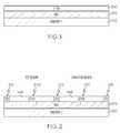
- FIG. 1is a cross-sectional view of a semiconductor structure after a first semiconductor layer has been formed on a buried insulator layer according to a first embodiment of the present invention
- FIG. 2is a cross-sectional view of the semiconductor structure of FIG. 1 after shallow trench isolation areas have been formed according to the first embodiment of the present invention
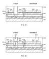
- FIG. 3is a cross-sectional view of the semiconductor structure of FIG. 1 after a dummy gate structure has been formed on an active area of a field-effect-transistor region according to the first embodiment of the present invention
- FIG. 4is a cross-sectional view of the semiconductor structure of FIG. 1 after a second semiconductor layer has been formed on the active area of the field-effect-transistor and capacitor regions according to the first embodiment of the present invention
- FIG. 5is a cross-sectional view of the semiconductor structure of FIG. 1 after a dielectric layer has been formed over the structure according to the first embodiment of the present invention
- FIG. 6is a cross-sectional view of the semiconductor structure of FIG. 1 after the dummy gate structure and a portion of the dielectric layer in the capacitor region have been removed according to the first embodiment of the present invention
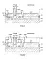
- FIG. 7is a cross-sectional view of the semiconductor structure of FIG. 1 after a high-k gate dielectric layer and a gate conductor layer have been formed in the field-effect-transistor region according to the first embodiment of the present invention
- FIG. 8is a cross-sectional view of the semiconductor structure of FIG. 1 after contacts have been formed in the field-effect-transistor region and the capacitor region according to the first embodiment of the present invention
- FIG. 9is a cross-sectional view of a semiconductor structure after a dielectric layer has been formed over a field-effect-transistor region and a capacitor region according to a second embodiment of the present invention.
- FIG. 10is a cross-sectional view of the semiconductor structure of FIG. 9 after portions of the dielectric layer have been removed in the field-effect-transistor region and the capacitor region according to the second embodiment of the present invention
- FIG. 11is a cross-sectional view of the semiconductor structure of FIG. 9 after silicide regions have been formed in the field-effect-transistor region and the capacitor region according to the second embodiment of the present invention
- FIG. 12is a cross-sectional view of the semiconductor structure of FIG. 9 after contacts have been formed in the field-effect-transistor region and the capacitor region according to the second embodiment of the present invention
- FIG. 13is an operational flow diagram illustrating a process for forming a fully depleted FET and an on-chip capacitor according to one embodiment of the present invention.
- FIG. 14is an operational flow diagram illustrating another process for forming a fully depleted FET and an on-chip capacitor according to another embodiment of the present invention.
- Embodiments of the present inventionprovide an integrated circuit that includes a fully depleted FET and an on-chip capacitor, and methods for forming such an integrated circuit.
- an on-chip capacitor and a fully depleted FETshare the same high-k dielectric and a metal layer, so as to greatly reduce process complexity and cost.
- the capacitorhas a low resistance silicide electrode and a low resistance metal electrode, so as to greatly improve the capacitor's electrical characteristics.
- the capacitoris formed during a trench silicide/contact formation process. This allows the capacitor to have a high-k dielectric layer made of a different material than the gate dielectric of the FET, so as to achieve better electrical characteristics for the FET and the capacitor.
- Embodiments of the present inventionare also applicable to other devices (such as finFETs and nanowire devices) in which epitaxial growth is used to form merged source/drains, as opposed to the raised source/drains of ETSOI devices.
- FIGS. 1 to 8illustrate a process for forming an integrated circuit that includes a fully depleted FET and an on-chip capacitor according to one embodiment of the present invention.
- an SOI waferhaving a silicon substrate 102 , a buried insulator layer such as a buried oxide (BOX) 104 , and a first semiconductor layer 106 such as an extremely thin silicon-on-insulator (ETSOI) layer.
- the ETSOI layer 106 of this embodimenthas a thickness ranging from about 1 nm to 20 nm, while in another embodiment the ETSOI layer 106 has a thickness ranging from about 3 nm to 10 nm.
- the SOI waferis formed by thinning a “thick” SOI wafer (with a thickness in the 30 nm to 90 nm range) using oxidation and a hydrofluoric acid (HF) wet etch.
- the ETSOI layer 106can be any semiconducting material, including but not limited to Si (silicon), strained Si, SiC (silicon carbide), Ge (geranium), SiGe (silicon germanium), SiGeC (silicon-germanium-carbon), Si alloys, Ge alloys, GaAs (gallium arsenide), InAs (indium arsenide), InP (indium phosphide), or any combination thereof.
- An active area 206 for the FET and an area 210 for the capacitorare then defined within the ETSOI layer 106 through pad-film deposition, patterning (e.g., by photolithography), and reactive-ion etching (RIE).
- RIEreactive-ion etching
- a pad oxide having a thickness of 2 nm to 10 nmis formed in an oxidation furnace, and a pad nitride is deposited over the pad oxide using low-pressure chemical vapor deposition (LPCVD) or rapid-thermal chemical vapor deposition (RTCVD).
- LPCVDlow-pressure chemical vapor deposition
- RTCVDrapid-thermal chemical vapor deposition
- Photolithography and a nitride-oxide-silicon RIEare then performed to define the active area 206 and capacitor area 210 .
- STIshallow trench isolation
- LOCOSLocal Oxidation Of Silicon for Isolation
- mesa isolationSTI
- STIis obtained through deposition of an STI oxide, densification anneals, and chemical-mechanical polishing (CMP) that stops on the pad nitride.
- CMPchemical-mechanical polishing
- the pad nitride, along with any STI oxide remaining on the pad nitride, and the pad oxideare then removed (e.g., through wet etching using hot phosphoric acid and HF).
- a dummy (or replacement) gate structure 318is then formed on the active area 206 of the FET, as shown in FIG. 3 .
- the dummy gate 318comprises multiple layers of oxide, polysilicon, amorphous silicon, nitride, or a combination thereof.
- the dummy gate 318can comprise a single layer such as a nitride layer.
- a gate spacer 320comprising a dielectric material (such as silicon oxide, silicon nitride, silicon oxynitride, or a combination of these) is formed on the sidewalls of the dummy gate 318 .
- the dielectric materialis formed and then reactive-ion etching is used to remove the dielectric material except from the sidewalls of the dummy gate 318 .
- an additional layer 421 and 423(“second semiconductor layer”) is formed on exposed surfaces of the ETSOI layer 106 in both the FET and capacitor regions.
- the additional layer 421 in the FET regioncomprises a first portion 422 and a second portion 424 located on the sides of the gate spacer 320 .
- the first portion 422is formed on the ETSOI layer 106 between the first STI region 212 and a first wall 417 of the gate spacer 320
- the second portion 424is formed between the second STI region 214 and a second wall 419 of the gate spacer 320 .
- Another portion of the additional layer 423is formed in the capacitor region over substantially the entire ETSOI layer 106 of the capacitor region.
- the additional layer 421 and 423is formed through epitaxial growth, and can be formed undoped or doped with either p-type or n-type dopants.
- the portions 422 and 424 of the additional layer in the FET regionform the raised source and drain regions of the FET.
- the deposited atomsarrive at the surface of the ETSOI layer 106 with sufficient energy to move around on the surface and orient themselves to the crystal arrangement of the atoms of the deposition surface.
- an epitaxial film deposited on a [100] crystal surfacewill take on a [100] orientation.
- the deposited atomshave no surface to align to and form polysilicon instead of single crystal silicon.
- Silicon sources for the epitaxial growthinclude silicon tetrachloride, dichlorosilane (SiH2Cl2), and silane (SiH4).
- the temperature for this epitaxial silicon depositionis from 550° C. to 900° C.
- the additional layeris formed through selective-epitaxial growth of SiGe atop the ETSOI layer 106 .
- the Ge content of the epitaxial grown SiGeranges from 5% to 60% (by atomic weight). In another embodiment, the Ge content of the epitaxially grown SiGe ranges from 10% to 40%.
- the epitaxially grown SiGe of the illustrated embodimentis under an intrinsic compressive strain that is produced by a lattice mismatch between the larger lattice dimension of the SiGe and the smaller lattice dimension of the layer on which the SiGe is epitaxially grown.
- the epitaxially grown SiGeproduces a compressive strain in the portion of the ETSOI layer 106 in which the channel of the semiconductor device is formed.
- the additional layer 421 and 423is doped with a first conductivity type dopant during the epitaxial growth process.
- P-type MOSFET devicesare produced by doping the additional layer with elements from group III of the periodic table (e.g., boron, aluminum, gallium, or indium).
- the dopantcan be boron in a concentration ranging from 1 ⁇ 10E18 atoms/cm3 to 2 ⁇ 10E21 atoms/cm3.
- the additional layeris composed of epitaxially grown Si:C (carbon doped silicon).
- the carbon (C) content of the epitaxially grown Si:Cranges from 0.3% to 10% (by atomic weight). In another embodiment, the carbon (C) content of the epitaxially grown Si:C ranges from 1% to 2%.
- the epitaxially grown Si:Cis under an intrinsic tensile strain that is produced by a lattice mismatch between the smaller lattice dimension of the Si:C and the larger lattice dimension of the layer on which the Si:C is epitaxially grown.
- the epitaxial grown Si:Cproduces a tensile strain in the ETSOI layer 106 in which the channel of the semiconductor device is formed.
- the additional layer 421 and 423is doped with a second conductivity type dopant during the epitaxial growth process.
- N-type MOSFET devicesare produced by doping the semiconductor material 208 with elements from group V of the periodic table (e.g., phosphorus, antimony, or arsenic).
- the additional layer 421 and 423is a doped dielectric such as a doped oxide, formed by deposition such as through atomic layer deposition (ALD), molecular layer deposition (MLD), chemical vapor deposition (CVD), low-pressure chemical vapor deposition (LPCVD), plasma enhanced chemical vapor deposition (PECVD), high density plasma chemical vapor deposition (HDPCVD), sub-atmospheric chemical vapor deposition (SACVD), rapid thermal chemical vapor deposition (RTCVD), in-situ radical assisted deposition, high temperature oxide deposition (HTO), low temperature oxide deposition (LTO), ozone/TEOS deposition, limited reaction processing CVD (LRPCVD), ultrahigh vacuum chemical vapor deposition (UHVCVD), metalorganic chemical vapor deposition (MOCVD), molecular beam epitaxy (MBE), physical vapor deposition, sputtering, plating, evaporation, spin-on-coating, ion beam deposition, electron beam deposition,
- the dopant in the additional layer 421 and 423is boron, arsenic, phosphorus, or indium, with a concentration ranging from 1 ⁇ 10E18 atoms/cm3 to 2 ⁇ 10E21 atoms/cm3.
- the portions 422 and 424 of the additional layer 421 in the FET regionprovides the raised source and drain regions of the FET.
- an implantation processcan be performed to implant the additional layer of the capacitor and to form the source/drain regions and source/drain extensions of the FET.
- photolithographyis used to selectively define NFET and PFET areas for deep source/drain and extension implants, and then ions are implanted. N-type species are implanted for NFETs, while P-type species are implanted for PFETs.
- a thermal annealis then performed to activate and diffuse the implanted ions so as to form the raised source/drain regions 427 and 428 and the source/drain extensions 430 and 432 , such as through a spike rapid-thermal anneal (RTA), and to also diffuse the implanted ions in the additional layer 423 of the capacitor.
- RTAspike rapid-thermal anneal
- annealingsuch as rapid thermal annealing, furnace annealing, flash lamp annealing, laser annealing, or any suitable combination thereof
- the source/drain regions 427 and 428are heavily doped with an N-type dopant, the source/drain extension regions 430 and 432 are lightly doped with the same or a different N-type dopant, and the halo regions are doped with a P-type dopant.
- the source/drain regions 427 and 428are heavily doped with a P-type dopant, the source/drain extension regions 430 and 432 are lightly doped with the same or a different P-type dopant, and the halo regions are doped with an N-type dopant.
- silicide areas 534 , 536 , and 538are formed for contacts on the raised source/drain regions 427 and 428 of the FET and the additional layer 423 of the capacitor.
- a metalis deposited on top of the raised source/drain regions 427 and 428 of the FET and the additional layer 423 of the capacitor.
- An annealis then performed to form silicide, and then the metal is selectively removed.
- the metalcan be nickel, cobalt, titanium, platinum, or an alloy or combination thereof.
- a first dielectric layer 540(e.g., an oxide layer, nitride layer, low-k material or any suitable combination of those materials) is formed over the entire structure, as shown in FIG. 5 .
- This dielectric layer 540is then etched down to the level of the top surface of the dummy gate 318 .
- the dummy gate 318is removed via selective etching or another technique to form a gate cavity 642 that exposes a portion 646 of the ETSOI layer 106 , as shown in FIG. 6 .
- a masking layeris then formed over the dielectric layer 540 and gate cavity 642 in the FET region, and also over portions of the silicide area 538 in the capacitor region.
- the unmasked area of the dielectric layer 540 of the capacitoris then removed by a patterning, (e.g., by photolithography followed by etching such as reactive-ion etching (RIE) process) to form a capacitor cavity 644 that exposes a portion of the silicide area 538 , as shown in FIG. 6 .
- RIEreactive-ion etching
- the capacitor cavitycan be formed prior to removing the dummy gate 318 .
- a high-k dielectric materialis blanket deposited, for example by CVD (chemical vapor deposition), PECVD (plasma enhanced chemical vapor deposition), or ALD (Atomic layer deposition) followed by depositing one or more conductive materials to form high-k gate dielectric and metal gate.
- CVDchemical vapor deposition
- PECVDplasma enhanced chemical vapor deposition
- ALDAtomic layer deposition
- the excessive conductive material and high-k gate dielectric above the dielectric layer 540can be removed, for example, by polishing such as chemically mechanical polishing (CMP) and/or etching to form a high-k gate dielectric 746 on the bottom (the exposed portion of the ETSOI layer 106 ) and vertical sidewalls of the gate cavity 642 of the FET region, and a high-k capacitor dielectric 748 on the bottom (the exposed portion of the silicide area 538 ) and vertical sidewalls of the capacitor cavity 644 , and a gate conductor 750 in the gate cavity 642 and a metal electrode (terminal) 752 in the capacitor cavity 644 , as shown in FIG. 7 .
- the gate conductor 750fills the remaining portion of the gate cavity 642 and the metal electrode 752 fills the remaining portion of the capacitor cavity 644 .
- high-k materialsinclude but are not limited to metal oxides such as hafnium oxide, hafnium silicon oxide, hafnium silicon oxynitride, lanthanum oxide, lanthanum aluminum oxide, zirconium oxide, zirconium silicon oxide, zirconium silicon oxynitride, tantalum oxide, titanium oxide, barium strontium titanium oxide, barium titanium oxide, strontium titanium oxide, yttrium oxide, aluminum oxide, lead scandium tantalum oxide, and lead zinc niobate.
- the high-kmay further include dopants such as lanthanum, aluminum.
- An interfacial layer(not shown) may be formed on top of the channel 208 before depositing high-k material.
- the interfacial layerincludes but is not limited to, silicon oxide, silicon nitride, silicon oxynitride that can be formed by chemical oxidation, low temperature oxidation, nitridation, and/or oxynitridation process.
- the conductive materialcomprises polycrystalline or amorphous silicon, germanium, silicon germanium, a metal (e.g., tungsten, titanium, tantalum, ruthenium, zirconium, cobalt, copper, aluminum, lead, platinum, tin, silver, gold), a conducting metallic compound material (e.g., tantalum nitride, titanium nitride, tungsten silicide, tungsten nitride, ruthenium oxide, cobalt silicide, nickel silicide), carbon nanotube, conductive carbon, or any suitable combination of these materials.
- the conductive materialmay further comprise dopants that are incorporated during or after deposition.
- the conductive materialmay comprises multiple layers such as gate workfunction setting layer and gate conductive layer.
- a second dielectric layer 853comprising an oxide layer, nitride layer, low-k material or any suitable combination of those materials, in this embodiment, is then formed over the entire structure, as shown in FIG. 8 .
- Contacts 854 , 856 , and 858are then formed for the silicide areas 534 and 536 and the gate conductor 750 of the FET.
- Contacts 860 , 862 , and 864are also formed to the silicide area 538 adjacent to the vertical sidewalls of the high-k capacitor dielectric 748 , and also to the metal electrode 752 , as shown in FIG. 8 .
- a conventional processis used to form the contacts.
- the above processproduces a FET having a high-k gate dielectric and a metal gate, and a capacitor having a metal electrode (terminal), high-k capacitor dielectric, and another electrode (terminal) comprising a silicide.
- a high-k/metal gate FET and a low resistance capacitorare fabricated simultaneously. Also, because the FET and capacitor are formed using the same dielectric and metal materials, low fabrication costs are achieved.
- FIGS. 9 to 12illustrate the relevant portion of a process for forming an integrated circuit that includes a fully depleted FET and an on-chip capacitor according to another embodiment of the present invention.
- the capacitoris formed during a trench silicide process.
- the dummy gate structure 318 and gate spacer 320are formed as described above. Then, prior to forming the additional layer 421 and 423 , the dummy gate 318 is removed to form a gate cavity 642 .
- a high-k dielectric layeris blanket deposited, for example by CVD (chemical vapor deposition), PECVD (plasma enhanced chemical vapor deposition), or ALD (Atomic layer deposition) followed by depositing one or more conductive materials to form high-k gate dielectric and metal gate.
- the excessive conductive material and high-k gate dielectric above the dielectric layer 540can be removed, for example, by polishing such as chemically mechanical polishing (CMP) and/or etching.
- CMPchemically mechanical polishing
- the gate conductor 750fills the remaining portion of the gate cavity 642 .
- the additional layer 421 and 423is then formed using the process described above.
- the source/drain regions 427 and 428 and the source/drain extensions 430 and 432are then formed.
- the source/drain regions 427 and 428are merged source/drains.
- a dielectric layer 540e.g., an oxide layer, nitride layer, low-k material or any suitable combination of those materials is then formed over the entire structure, as shown in FIG. 9 .
- portions of the dielectric layer 540 over the additional layer 421 and 423are removed (e.g., through a dry etch such as RIE and/or a wet etch using HF) so as to create contact trenches/openings 1066 and 1068 in the FET region, and a capacitor trench/opening 644 in the capacitor region, as shown in FIG. 10 .
- Silicide regions 534 , 536 , and 538are then formed within the contact openings 1066 and 1068 and the capacitor cavity 644 , as shown in FIG. 11 .
- a metalis deposited on top of the source/drain regions 427 and 428 and the additional layer 423 of the capacitor. An anneal is then performed to form silicide, and then the metal is selectively removed.
- the metalis nickel, cobalt, titanium, platinum, or an alloy or combination thereof.
- a high-k dielectric materialis blanket deposited, for example by CVD (chemical vapor deposition), PECVD (plasma enhanced chemical vapor deposition), or ALD (Atomic layer deposition) followed by depositing one or more conductive materials to form high-k gate dielectric and metal gate for the capacitor.
- CVDchemical vapor deposition
- PECVDplasma enhanced chemical vapor deposition
- ALDAtomic layer deposition
- the excessive conductive material and high-k gate dielectric above the dielectric layer 540can be removed, for example, by polishing such as chemically mechanical polishing (CMP) and/or etching to form a high-k capacitor dielectric 748 on the bottom (the exposed portion of the silicide area 538 ) and vertical sidewalls of the capacitor cavity 644 , and a metal electrode (terminal) 1252 in the capacitor cavity 644 , as shown in FIG. 12 .
- the metal electrode 1252fills the remaining portion of the capacitor cavity 644 .
- the capacitor and the transistorcan have same high-k dielectric material, but with different thicknesses.
- contacts 1254 and 1256are then formed for the silicide areas 534 and 536 and in the contact openings 1066 and 1068 , as shown in FIG. 12 .
- a conventional processis used to form the contacts.
- FIG. 13is an operational flow diagram illustrating a process for forming an integrated circuit that includes a fully depleted FET and an on-chip capacitor according to one embodiment of the present invention.
- a transistor region and a capacitor regionare defined in a first semiconductor layer, at step 1304 .
- a dummy gate structureis formed on the first semiconductor layer in the transistor region, at step 1306 .
- a gate spaceris formed on vertical sidewalls of the dummy gate structure, at step 1308 .
- a second semiconductor layeris formed adjacent to each side of the gate spacer on the first semiconductor layer, and a third semiconductor layer is formed on the first semiconductor layer in the capacitor region, at step 1310 .
- a first silicide region and a second silicide regionare formed on the second semiconductor layer, and a third silicide region is formed on the third semiconductor layer, at step 1312 .
- an oxide layeris formed on the silicide regions and the gate spacer, at step 1314 .
- the dummy gate structureis removed so as to form a first cavity, at step 1316 .
- a portion of the oxide layer formed on the third silicide regionis removed so as to form a second cavity, at step 1318 .
- a gate dielectricis formed in the first cavity and a capacitor dielectric is formed in the second cavity, at step 1320 .
- a gate conductoris formed in the first cavity abutting the gate dielectric, and a metal electrode is formed within the second cavity abutting the capacitor dielectric, at step 1322 .
- Contactsare then formed on the silicide areas and the gate conductor of the FET, and contacts are also formed on portions of the silicide area that are adjacent to the vertical sidewalls of the high-k capacitor dielectric, and also on a portion of the metal electrode, at step 1324 .
- FIG. 14is an operational flow diagram illustrating a process for forming an integrated circuit that includes a fully depleted FET and an on-chip capacitor according to another embodiment of the present invention.
- a transistor region and a capacitor regionare defined/isolated in a first semiconductor layer, at step 1404 .
- a dummy gate structureis formed on the first semiconductor layer in the transistor region, at step 1406 .
- a gate spaceris formed on vertical sidewalls of the dummy gate structure, at step 1408 .
- a second semiconductor layeris formed adjacent to each side of the gate spacer on the first semiconductor layer, and a third semiconductor layer is formed on the first semiconductor layer in the capacitor region, at step 1410 .
- An oxide layeris then formed on the gate spacer and the second and third semiconductor layers, at step 1412 .
- the dummy gate structureis removed so as to form a first cavity, at step 1414 .
- a gate dielectricis formed in the first cavity, and a gate conductor is formed in the first cavity abutting the gate dielectric, at step 1416 .
- Trenchesare formed within the oxide layer to expose areas of the second semiconductor layer that are adjacent to the sides of the gate spacer, and a second cavity is formed in the oxide layer exposing an area of the third semiconductor layer, at step 1418 .
- a first silicide region and a second silicide regionare formed within the trenches on the second semiconductor layer, and a third silicide region is formed on the third semiconductor layer, at step 1420 .
- a capacitor dielectricis formed at least on the third silicide region and vertical sidewalls of the second cavity, at step 1422 .
- Metalized contactsare formed within the trenches for the FET, and a metal electrode for the capacitor is formed within the second cavity abutting the capacitor dielectric, at step 1424 .
- the circuit as described aboveis part of the design for an integrated circuit chip.
- the chip designis created in a graphical computer programming language, and stored in a computer storage medium (such as a disk, tape, physical hard drive, or virtual hard drive such as in a storage access network). If the designer does not fabricate chips or the photolithographic masks used to fabricate chips, the designer transmits the resulting design by physical means (e.g., by providing a copy of the storage medium storing the design) or electronically (e.g., through the Internet) to such entities, directly or indirectly.
- the stored designis then converted into the appropriate format (e.g., GDSII) for the fabrication of photolithographic masks, which typically include multiple copies of the chip design in question that are to be formed on a wafer.
- the photolithographic masksare utilized to define areas of the wafer (and/or the layers thereon) to be etched or otherwise processed.
- the resulting integrated circuit chipscan be distributed by the fabricator in raw wafer form (that is, as a single wafer that has multiple unpackaged chips), as a bare chip, or in a packaged form.
- the chipis mounted in a single chip package (such as a plastic carrier, with leads that are affixed to a motherboard or other higher level carrier) or in a multichip package (such as a ceramic carrier that has either or both surface interconnections or buried interconnections).
- the chipis then integrated with other chips, discrete circuit elements, and/or other signal processing devices as part of either (a) an intermediate product, such as a motherboard, or (b) an end product.
- the end productcan be any product that includes integrated circuit chips, ranging from toys and other low-end applications to advanced computer products (such as, but not limited to, an information processing system) having a display, a keyboard, or other input device, and a central processor.
- the terms “a” or “an”, as used herein,are defined as one as or more than one.
- the term plurality, as used herein,is defined as two as or more than two. Plural and singular terms are the same unless expressly stated otherwise.
- the term another, as used herein,is defined as at least a second or more.
- the terms including and/or having, as used herein,are defined as comprising (i.e., open language).
- the term coupled, as used herein,is defined as connected, although not necessarily directly, and not necessarily mechanically.
- program, software application, and the like as used hereinare defined as a sequence of instructions designed for execution on a computer system.
- a program, computer program, or software applicationmay include a subroutine, a function, a procedure, an object method, an object implementation, an executable application, an applet, a servlet, a source code, an object code, a shared library/dynamic load library and/or other sequence of instructions designed for execution on a computer system.
Landscapes
- Engineering & Computer Science (AREA)
- Physics & Mathematics (AREA)
- Condensed Matter Physics & Semiconductors (AREA)
- General Physics & Mathematics (AREA)
- Manufacturing & Machinery (AREA)
- Computer Hardware Design (AREA)
- Microelectronics & Electronic Packaging (AREA)
- Power Engineering (AREA)
- Thin Film Transistor (AREA)
- Metal-Oxide And Bipolar Metal-Oxide Semiconductor Integrated Circuits (AREA)
- Semiconductor Integrated Circuits (AREA)
Abstract
Description
Claims (12)
Priority Applications (4)
| Application Number | Priority Date | Filing Date | Title |
|---|---|---|---|
| US13/345,266US8659066B2 (en) | 2012-01-06 | 2012-01-06 | Integrated circuit with a thin body field effect transistor and capacitor |
| US13/614,908US8652898B2 (en) | 2012-01-06 | 2012-09-13 | Integrated circuit with a thin body field effect transistor and capacitor |
| US14/164,310US9245807B2 (en) | 2012-01-06 | 2014-01-27 | Integrated circuit with a thin body field effect transistor and capacitor |
| US14/168,208US9070788B2 (en) | 2012-01-06 | 2014-01-30 | Integrated circuit with a thin body field effect transistor and capacitor |
Applications Claiming Priority (1)
| Application Number | Priority Date | Filing Date | Title |
|---|---|---|---|
| US13/345,266US8659066B2 (en) | 2012-01-06 | 2012-01-06 | Integrated circuit with a thin body field effect transistor and capacitor |
Related Child Applications (2)
| Application Number | Title | Priority Date | Filing Date |
|---|---|---|---|
| US13/614,908ContinuationUS8652898B2 (en) | 2012-01-06 | 2012-09-13 | Integrated circuit with a thin body field effect transistor and capacitor |
| US14/168,208ContinuationUS9070788B2 (en) | 2012-01-06 | 2014-01-30 | Integrated circuit with a thin body field effect transistor and capacitor |
Publications (2)
| Publication Number | Publication Date |
|---|---|
| US20130175596A1 US20130175596A1 (en) | 2013-07-11 |
| US8659066B2true US8659066B2 (en) | 2014-02-25 |
Family
ID=48743332
Family Applications (4)
| Application Number | Title | Priority Date | Filing Date |
|---|---|---|---|
| US13/345,266ActiveUS8659066B2 (en) | 2012-01-06 | 2012-01-06 | Integrated circuit with a thin body field effect transistor and capacitor |
| US13/614,908Expired - Fee RelatedUS8652898B2 (en) | 2012-01-06 | 2012-09-13 | Integrated circuit with a thin body field effect transistor and capacitor |
| US14/164,310Expired - Fee RelatedUS9245807B2 (en) | 2012-01-06 | 2014-01-27 | Integrated circuit with a thin body field effect transistor and capacitor |
| US14/168,208ActiveUS9070788B2 (en) | 2012-01-06 | 2014-01-30 | Integrated circuit with a thin body field effect transistor and capacitor |
Family Applications After (3)
| Application Number | Title | Priority Date | Filing Date |
|---|---|---|---|
| US13/614,908Expired - Fee RelatedUS8652898B2 (en) | 2012-01-06 | 2012-09-13 | Integrated circuit with a thin body field effect transistor and capacitor |
| US14/164,310Expired - Fee RelatedUS9245807B2 (en) | 2012-01-06 | 2014-01-27 | Integrated circuit with a thin body field effect transistor and capacitor |
| US14/168,208ActiveUS9070788B2 (en) | 2012-01-06 | 2014-01-30 | Integrated circuit with a thin body field effect transistor and capacitor |
Country Status (1)
| Country | Link |
|---|---|
| US (4) | US8659066B2 (en) |
Cited By (1)
| Publication number | Priority date | Publication date | Assignee | Title |
|---|---|---|---|---|
| US20170194418A1 (en)* | 2015-12-30 | 2017-07-06 | Teledyne Scientific & Imaging, Llc | Vertical capacitor contact arrangement and fabrication method |
Families Citing this family (387)
| Publication number | Priority date | Publication date | Assignee | Title |
|---|---|---|---|---|
| US10378106B2 (en) | 2008-11-14 | 2019-08-13 | Asm Ip Holding B.V. | Method of forming insulation film by modified PEALD |
| US9394608B2 (en) | 2009-04-06 | 2016-07-19 | Asm America, Inc. | Semiconductor processing reactor and components thereof |
| US8802201B2 (en) | 2009-08-14 | 2014-08-12 | Asm America, Inc. | Systems and methods for thin-film deposition of metal oxides using excited nitrogen-oxygen species |
| US9312155B2 (en) | 2011-06-06 | 2016-04-12 | Asm Japan K.K. | High-throughput semiconductor-processing apparatus equipped with multiple dual-chamber modules |
| US10364496B2 (en) | 2011-06-27 | 2019-07-30 | Asm Ip Holding B.V. | Dual section module having shared and unshared mass flow controllers |
| US10854498B2 (en) | 2011-07-15 | 2020-12-01 | Asm Ip Holding B.V. | Wafer-supporting device and method for producing same |
| US20130023129A1 (en) | 2011-07-20 | 2013-01-24 | Asm America, Inc. | Pressure transmitter for a semiconductor processing environment |
| US9017481B1 (en) | 2011-10-28 | 2015-04-28 | Asm America, Inc. | Process feed management for semiconductor substrate processing |
| JP5968708B2 (en) | 2012-01-23 | 2016-08-10 | ルネサスエレクトロニクス株式会社 | Semiconductor device |
| US9659799B2 (en) | 2012-08-28 | 2017-05-23 | Asm Ip Holding B.V. | Systems and methods for dynamic semiconductor process scheduling |
| US9021985B2 (en) | 2012-09-12 | 2015-05-05 | Asm Ip Holdings B.V. | Process gas management for an inductively-coupled plasma deposition reactor |
| US9748356B2 (en) | 2012-09-25 | 2017-08-29 | Stmicroelectronics, Inc. | Threshold adjustment for quantum dot array devices with metal source and drain |
| US9601630B2 (en)* | 2012-09-25 | 2017-03-21 | Stmicroelectronics, Inc. | Transistors incorporating metal quantum dots into doped source and drain regions |
| US10714315B2 (en) | 2012-10-12 | 2020-07-14 | Asm Ip Holdings B.V. | Semiconductor reaction chamber showerhead |
| US9012966B2 (en)* | 2012-11-21 | 2015-04-21 | Qualcomm Incorporated | Capacitor using middle of line (MOL) conductive layers |
| US9029208B2 (en)* | 2012-11-30 | 2015-05-12 | International Business Machines Corporation | Semiconductor device with replacement metal gate and method for selective deposition of material for replacement metal gate |
| US20160376700A1 (en) | 2013-02-01 | 2016-12-29 | Asm Ip Holding B.V. | System for treatment of deposition reactor |
| US9484191B2 (en) | 2013-03-08 | 2016-11-01 | Asm Ip Holding B.V. | Pulsed remote plasma method and system |
| US9589770B2 (en) | 2013-03-08 | 2017-03-07 | Asm Ip Holding B.V. | Method and systems for in-situ formation of intermediate reactive species |
| US9093285B2 (en) | 2013-03-22 | 2015-07-28 | United Microelectronics Corp. | Semiconductor structure and process thereof |
| US10002938B2 (en) | 2013-08-20 | 2018-06-19 | Stmicroelectronics, Inc. | Atomic layer deposition of selected molecular clusters |
| US9240412B2 (en) | 2013-09-27 | 2016-01-19 | Asm Ip Holding B.V. | Semiconductor structure and device and methods of forming same using selective epitaxial process |
| US10683571B2 (en) | 2014-02-25 | 2020-06-16 | Asm Ip Holding B.V. | Gas supply manifold and method of supplying gases to chamber using same |
| US10167557B2 (en) | 2014-03-18 | 2019-01-01 | Asm Ip Holding B.V. | Gas distribution system, reactor including the system, and methods of using the same |
| US11015245B2 (en) | 2014-03-19 | 2021-05-25 | Asm Ip Holding B.V. | Gas-phase reactor and system having exhaust plenum and components thereof |
| US9245903B2 (en)* | 2014-04-11 | 2016-01-26 | International Business Machines Corporation | High voltage metal oxide semiconductor field effect transistor integrated into extremely thin semiconductor on insulator process |
| US9543440B2 (en)* | 2014-06-20 | 2017-01-10 | International Business Machines Corporation | High density vertical nanowire stack for field effect transistor |
| US10858737B2 (en) | 2014-07-28 | 2020-12-08 | Asm Ip Holding B.V. | Showerhead assembly and components thereof |
| US9754935B2 (en)* | 2014-08-07 | 2017-09-05 | International Business Machines Corporation | Raised metal semiconductor alloy for self-aligned middle-of-line contact |
| US9890456B2 (en) | 2014-08-21 | 2018-02-13 | Asm Ip Holding B.V. | Method and system for in situ formation of gas-phase compounds |
| US9657845B2 (en) | 2014-10-07 | 2017-05-23 | Asm Ip Holding B.V. | Variable conductance gas distribution apparatus and method |
| US10941490B2 (en) | 2014-10-07 | 2021-03-09 | Asm Ip Holding B.V. | Multiple temperature range susceptor, assembly, reactor and system including the susceptor, and methods of using the same |
| KR102300403B1 (en) | 2014-11-19 | 2021-09-09 | 에이에스엠 아이피 홀딩 비.브이. | Method of depositing thin film |
| KR102263121B1 (en) | 2014-12-22 | 2021-06-09 | 에이에스엠 아이피 홀딩 비.브이. | Semiconductor device and manufacuring method thereof |
| US9443871B2 (en)* | 2015-01-08 | 2016-09-13 | Globalfoundries Inc. | Cointegration of bulk and SOI semiconductor devices |
| US9570578B2 (en)* | 2015-02-11 | 2017-02-14 | United Microelectronics Corp. | Gate and gate forming process |
| US10529542B2 (en) | 2015-03-11 | 2020-01-07 | Asm Ip Holdings B.V. | Cross-flow reactor and method |
| US10276355B2 (en) | 2015-03-12 | 2019-04-30 | Asm Ip Holding B.V. | Multi-zone reactor, system including the reactor, and method of using the same |
| KR102271239B1 (en)* | 2015-03-23 | 2021-06-29 | 삼성전자주식회사 | Semiconductor device and method for fabricating the same |
| US9536974B2 (en)* | 2015-04-17 | 2017-01-03 | Globalfoundries Inc. | FET device with tuned gate work function |
| US10458018B2 (en) | 2015-06-26 | 2019-10-29 | Asm Ip Holding B.V. | Structures including metal carbide material, devices including the structures, and methods of forming same |
| US10600673B2 (en) | 2015-07-07 | 2020-03-24 | Asm Ip Holding B.V. | Magnetic susceptor to baseplate seal |
| US10043661B2 (en) | 2015-07-13 | 2018-08-07 | Asm Ip Holding B.V. | Method for protecting layer by forming hydrocarbon-based extremely thin film |
| US10083836B2 (en) | 2015-07-24 | 2018-09-25 | Asm Ip Holding B.V. | Formation of boron-doped titanium metal films with high work function |
| US9768254B2 (en)* | 2015-07-30 | 2017-09-19 | International Business Machines Corporation | Leakage-free implantation-free ETSOI transistors |
| US9490252B1 (en) | 2015-08-05 | 2016-11-08 | International Business Machines Corporation | MIM capacitor formation in RMG module |
| US10312318B2 (en)* | 2015-09-22 | 2019-06-04 | International Business Machines Corporation | Metal-insulator-metal capacitor structure |
| US9691897B2 (en)* | 2015-09-28 | 2017-06-27 | Globalfoundries Inc. | Three-dimensional semiconductor transistor with gate contact in active region |
| US9960072B2 (en) | 2015-09-29 | 2018-05-01 | Asm Ip Holding B.V. | Variable adjustment for precise matching of multiple chamber cavity housings |
| US10211308B2 (en) | 2015-10-21 | 2019-02-19 | Asm Ip Holding B.V. | NbMC layers |
| US10322384B2 (en) | 2015-11-09 | 2019-06-18 | Asm Ip Holding B.V. | Counter flow mixer for process chamber |
| US11139308B2 (en) | 2015-12-29 | 2021-10-05 | Asm Ip Holding B.V. | Atomic layer deposition of III-V compounds to form V-NAND devices |
| US10529554B2 (en) | 2016-02-19 | 2020-01-07 | Asm Ip Holding B.V. | Method for forming silicon nitride film selectively on sidewalls or flat surfaces of trenches |
| US10468251B2 (en) | 2016-02-19 | 2019-11-05 | Asm Ip Holding B.V. | Method for forming spacers using silicon nitride film for spacer-defined multiple patterning |
| US10501866B2 (en) | 2016-03-09 | 2019-12-10 | Asm Ip Holding B.V. | Gas distribution apparatus for improved film uniformity in an epitaxial system |
| US10343920B2 (en) | 2016-03-18 | 2019-07-09 | Asm Ip Holding B.V. | Aligned carbon nanotubes |
| US9892913B2 (en) | 2016-03-24 | 2018-02-13 | Asm Ip Holding B.V. | Radial and thickness control via biased multi-port injection settings |
| US10865475B2 (en) | 2016-04-21 | 2020-12-15 | Asm Ip Holding B.V. | Deposition of metal borides and silicides |
| US10087522B2 (en) | 2016-04-21 | 2018-10-02 | Asm Ip Holding B.V. | Deposition of metal borides |
| US10190213B2 (en) | 2016-04-21 | 2019-01-29 | Asm Ip Holding B.V. | Deposition of metal borides |
| US10032628B2 (en)* | 2016-05-02 | 2018-07-24 | Asm Ip Holding B.V. | Source/drain performance through conformal solid state doping |
| US10367080B2 (en) | 2016-05-02 | 2019-07-30 | Asm Ip Holding B.V. | Method of forming a germanium oxynitride film |
| KR102592471B1 (en) | 2016-05-17 | 2023-10-20 | 에이에스엠 아이피 홀딩 비.브이. | Method of forming metal interconnection and method of fabricating semiconductor device using the same |
| US11453943B2 (en) | 2016-05-25 | 2022-09-27 | Asm Ip Holding B.V. | Method for forming carbon-containing silicon/metal oxide or nitride film by ALD using silicon precursor and hydrocarbon precursor |
| US10388509B2 (en) | 2016-06-28 | 2019-08-20 | Asm Ip Holding B.V. | Formation of epitaxial layers via dislocation filtering |
| US9859151B1 (en) | 2016-07-08 | 2018-01-02 | Asm Ip Holding B.V. | Selective film deposition method to form air gaps |
| US10612137B2 (en) | 2016-07-08 | 2020-04-07 | Asm Ip Holdings B.V. | Organic reactants for atomic layer deposition |
| US9793135B1 (en) | 2016-07-14 | 2017-10-17 | ASM IP Holding B.V | Method of cyclic dry etching using etchant film |
| US10714385B2 (en) | 2016-07-19 | 2020-07-14 | Asm Ip Holding B.V. | Selective deposition of tungsten |
| KR102354490B1 (en) | 2016-07-27 | 2022-01-21 | 에이에스엠 아이피 홀딩 비.브이. | Method of processing a substrate |
| US10395919B2 (en) | 2016-07-28 | 2019-08-27 | Asm Ip Holding B.V. | Method and apparatus for filling a gap |
| KR102532607B1 (en) | 2016-07-28 | 2023-05-15 | 에이에스엠 아이피 홀딩 비.브이. | Substrate processing apparatus and method of operating the same |
| US10177025B2 (en) | 2016-07-28 | 2019-01-08 | Asm Ip Holding B.V. | Method and apparatus for filling a gap |
| US9887082B1 (en) | 2016-07-28 | 2018-02-06 | Asm Ip Holding B.V. | Method and apparatus for filling a gap |
| US9812320B1 (en) | 2016-07-28 | 2017-11-07 | Asm Ip Holding B.V. | Method and apparatus for filling a gap |
| US9728543B1 (en)* | 2016-08-15 | 2017-08-08 | Taiwan Semiconductor Manufacturing Co., Ltd. | Semiconductor structure and fabricating method thereof |
| US10418364B2 (en)* | 2016-08-31 | 2019-09-17 | Globalfoundries Inc. | Semiconductor device structure with self-aligned capacitor device |
| US10090316B2 (en) | 2016-09-01 | 2018-10-02 | Asm Ip Holding B.V. | 3D stacked multilayer semiconductor memory using doped select transistor channel |
| US10410943B2 (en) | 2016-10-13 | 2019-09-10 | Asm Ip Holding B.V. | Method for passivating a surface of a semiconductor and related systems |
| US10643826B2 (en) | 2016-10-26 | 2020-05-05 | Asm Ip Holdings B.V. | Methods for thermally calibrating reaction chambers |
| US11532757B2 (en) | 2016-10-27 | 2022-12-20 | Asm Ip Holding B.V. | Deposition of charge trapping layers |
| US10643904B2 (en) | 2016-11-01 | 2020-05-05 | Asm Ip Holdings B.V. | Methods for forming a semiconductor device and related semiconductor device structures |
| US10229833B2 (en) | 2016-11-01 | 2019-03-12 | Asm Ip Holding B.V. | Methods for forming a transition metal nitride film on a substrate by atomic layer deposition and related semiconductor device structures |
| US10714350B2 (en) | 2016-11-01 | 2020-07-14 | ASM IP Holdings, B.V. | Methods for forming a transition metal niobium nitride film on a substrate by atomic layer deposition and related semiconductor device structures |
| US10435790B2 (en) | 2016-11-01 | 2019-10-08 | Asm Ip Holding B.V. | Method of subatmospheric plasma-enhanced ALD using capacitively coupled electrodes with narrow gap |
| US10134757B2 (en) | 2016-11-07 | 2018-11-20 | Asm Ip Holding B.V. | Method of processing a substrate and a device manufactured by using the method |
| KR102546317B1 (en) | 2016-11-15 | 2023-06-21 | 에이에스엠 아이피 홀딩 비.브이. | Gas supply unit and substrate processing apparatus including the same |
| US10340135B2 (en) | 2016-11-28 | 2019-07-02 | Asm Ip Holding B.V. | Method of topologically restricted plasma-enhanced cyclic deposition of silicon or metal nitride |
| KR102491538B1 (en)* | 2016-11-30 | 2023-01-20 | 삼성전자주식회사 | Semiconductor device and method for fabricating the same |
| KR102762543B1 (en) | 2016-12-14 | 2025-02-05 | 에이에스엠 아이피 홀딩 비.브이. | Substrate processing apparatus |
| US9916980B1 (en) | 2016-12-15 | 2018-03-13 | Asm Ip Holding B.V. | Method of forming a structure on a substrate |
| US11447861B2 (en) | 2016-12-15 | 2022-09-20 | Asm Ip Holding B.V. | Sequential infiltration synthesis apparatus and a method of forming a patterned structure |
| US11581186B2 (en) | 2016-12-15 | 2023-02-14 | Asm Ip Holding B.V. | Sequential infiltration synthesis apparatus |
| KR102700194B1 (en) | 2016-12-19 | 2024-08-28 | 에이에스엠 아이피 홀딩 비.브이. | Substrate processing apparatus |
| US10269558B2 (en) | 2016-12-22 | 2019-04-23 | Asm Ip Holding B.V. | Method of forming a structure on a substrate |
| US10867788B2 (en) | 2016-12-28 | 2020-12-15 | Asm Ip Holding B.V. | Method of forming a structure on a substrate |
| US11390950B2 (en) | 2017-01-10 | 2022-07-19 | Asm Ip Holding B.V. | Reactor system and method to reduce residue buildup during a film deposition process |
| US9991267B1 (en)* | 2017-01-25 | 2018-06-05 | International Business Machines Corporation | Forming eDRAM unit cell with VFET and via capacitance |
| US10655221B2 (en) | 2017-02-09 | 2020-05-19 | Asm Ip Holding B.V. | Method for depositing oxide film by thermal ALD and PEALD |
| US10468261B2 (en) | 2017-02-15 | 2019-11-05 | Asm Ip Holding B.V. | Methods for forming a metallic film on a substrate by cyclical deposition and related semiconductor device structures |
| US10263013B2 (en)* | 2017-02-24 | 2019-04-16 | Globalfoundries Inc. | Method of forming an integrated circuit (IC) with hallow trench isolation (STI) regions and the resulting IC structure |
| US10283353B2 (en) | 2017-03-29 | 2019-05-07 | Asm Ip Holding B.V. | Method of reforming insulating film deposited on substrate with recess pattern |
| US10529563B2 (en) | 2017-03-29 | 2020-01-07 | Asm Ip Holdings B.V. | Method for forming doped metal oxide films on a substrate by cyclical deposition and related semiconductor device structures |
| US10103040B1 (en) | 2017-03-31 | 2018-10-16 | Asm Ip Holding B.V. | Apparatus and method for manufacturing a semiconductor device |
| USD830981S1 (en) | 2017-04-07 | 2018-10-16 | Asm Ip Holding B.V. | Susceptor for semiconductor substrate processing apparatus |
| KR102457289B1 (en) | 2017-04-25 | 2022-10-21 | 에이에스엠 아이피 홀딩 비.브이. | Method for depositing a thin film and manufacturing a semiconductor device |
| US10892156B2 (en) | 2017-05-08 | 2021-01-12 | Asm Ip Holding B.V. | Methods for forming a silicon nitride film on a substrate and related semiconductor device structures |
| US10770286B2 (en) | 2017-05-08 | 2020-09-08 | Asm Ip Holdings B.V. | Methods for selectively forming a silicon nitride film on a substrate and related semiconductor device structures |
| US10446393B2 (en) | 2017-05-08 | 2019-10-15 | Asm Ip Holding B.V. | Methods for forming silicon-containing epitaxial layers and related semiconductor device structures |
| US10504742B2 (en) | 2017-05-31 | 2019-12-10 | Asm Ip Holding B.V. | Method of atomic layer etching using hydrogen plasma |
| US10886123B2 (en) | 2017-06-02 | 2021-01-05 | Asm Ip Holding B.V. | Methods for forming low temperature semiconductor layers and related semiconductor device structures |
| US12040200B2 (en) | 2017-06-20 | 2024-07-16 | Asm Ip Holding B.V. | Semiconductor processing apparatus and methods for calibrating a semiconductor processing apparatus |
| US11306395B2 (en) | 2017-06-28 | 2022-04-19 | Asm Ip Holding B.V. | Methods for depositing a transition metal nitride film on a substrate by atomic layer deposition and related deposition apparatus |
| US10685834B2 (en) | 2017-07-05 | 2020-06-16 | Asm Ip Holdings B.V. | Methods for forming a silicon germanium tin layer and related semiconductor device structures |
| KR20190009245A (en) | 2017-07-18 | 2019-01-28 | 에이에스엠 아이피 홀딩 비.브이. | Methods for forming a semiconductor device structure and related semiconductor device structures |
| US11018002B2 (en) | 2017-07-19 | 2021-05-25 | Asm Ip Holding B.V. | Method for selectively depositing a Group IV semiconductor and related semiconductor device structures |
| US10541333B2 (en) | 2017-07-19 | 2020-01-21 | Asm Ip Holding B.V. | Method for depositing a group IV semiconductor and related semiconductor device structures |
| US11374112B2 (en) | 2017-07-19 | 2022-06-28 | Asm Ip Holding B.V. | Method for depositing a group IV semiconductor and related semiconductor device structures |
| US10590535B2 (en) | 2017-07-26 | 2020-03-17 | Asm Ip Holdings B.V. | Chemical treatment, deposition and/or infiltration apparatus and method for using the same |
| US10605530B2 (en) | 2017-07-26 | 2020-03-31 | Asm Ip Holding B.V. | Assembly of a liner and a flange for a vertical furnace as well as the liner and the vertical furnace |
| US10312055B2 (en) | 2017-07-26 | 2019-06-04 | Asm Ip Holding B.V. | Method of depositing film by PEALD using negative bias |
| TWI815813B (en) | 2017-08-04 | 2023-09-21 | 荷蘭商Asm智慧財產控股公司 | Showerhead assembly for distributing a gas within a reaction chamber |
| US10692741B2 (en) | 2017-08-08 | 2020-06-23 | Asm Ip Holdings B.V. | Radiation shield |
| US10770336B2 (en) | 2017-08-08 | 2020-09-08 | Asm Ip Holding B.V. | Substrate lift mechanism and reactor including same |
| US11139191B2 (en) | 2017-08-09 | 2021-10-05 | Asm Ip Holding B.V. | Storage apparatus for storing cassettes for substrates and processing apparatus equipped therewith |
| US10249524B2 (en) | 2017-08-09 | 2019-04-02 | Asm Ip Holding B.V. | Cassette holder assembly for a substrate cassette and holding member for use in such assembly |
| US11769682B2 (en) | 2017-08-09 | 2023-09-26 | Asm Ip Holding B.V. | Storage apparatus for storing cassettes for substrates and processing apparatus equipped therewith |
| US10236177B1 (en) | 2017-08-22 | 2019-03-19 | ASM IP Holding B.V.. | Methods for depositing a doped germanium tin semiconductor and related semiconductor device structures |
| USD900036S1 (en) | 2017-08-24 | 2020-10-27 | Asm Ip Holding B.V. | Heater electrical connector and adapter |
| US11830730B2 (en) | 2017-08-29 | 2023-11-28 | Asm Ip Holding B.V. | Layer forming method and apparatus |
| US11295980B2 (en) | 2017-08-30 | 2022-04-05 | Asm Ip Holding B.V. | Methods for depositing a molybdenum metal film over a dielectric surface of a substrate by a cyclical deposition process and related semiconductor device structures |
| KR102491945B1 (en) | 2017-08-30 | 2023-01-26 | 에이에스엠 아이피 홀딩 비.브이. | Substrate processing apparatus |
| US11056344B2 (en) | 2017-08-30 | 2021-07-06 | Asm Ip Holding B.V. | Layer forming method |
| KR102401446B1 (en) | 2017-08-31 | 2022-05-24 | 에이에스엠 아이피 홀딩 비.브이. | Substrate processing apparatus |
| US10607895B2 (en) | 2017-09-18 | 2020-03-31 | Asm Ip Holdings B.V. | Method for forming a semiconductor device structure comprising a gate fill metal |
| KR102630301B1 (en) | 2017-09-21 | 2024-01-29 | 에이에스엠 아이피 홀딩 비.브이. | Method of sequential infiltration synthesis treatment of infiltrateable material and structures and devices formed using same |
| US10844484B2 (en) | 2017-09-22 | 2020-11-24 | Asm Ip Holding B.V. | Apparatus for dispensing a vapor phase reactant to a reaction chamber and related methods |
| US10658205B2 (en) | 2017-09-28 | 2020-05-19 | Asm Ip Holdings B.V. | Chemical dispensing apparatus and methods for dispensing a chemical to a reaction chamber |
| US10403504B2 (en) | 2017-10-05 | 2019-09-03 | Asm Ip Holding B.V. | Method for selectively depositing a metallic film on a substrate |
| US10319588B2 (en) | 2017-10-10 | 2019-06-11 | Asm Ip Holding B.V. | Method for depositing a metal chalcogenide on a substrate by cyclical deposition |
| US10923344B2 (en) | 2017-10-30 | 2021-02-16 | Asm Ip Holding B.V. | Methods for forming a semiconductor structure and related semiconductor structures |
| US10910262B2 (en) | 2017-11-16 | 2021-02-02 | Asm Ip Holding B.V. | Method of selectively depositing a capping layer structure on a semiconductor device structure |
| KR102443047B1 (en) | 2017-11-16 | 2022-09-14 | 에이에스엠 아이피 홀딩 비.브이. | Method of processing a substrate and a device manufactured by the same |
| US11022879B2 (en) | 2017-11-24 | 2021-06-01 | Asm Ip Holding B.V. | Method of forming an enhanced unexposed photoresist layer |
| CN111344522B (en) | 2017-11-27 | 2022-04-12 | 阿斯莫Ip控股公司 | Including clean mini-environment device |
| WO2019103613A1 (en) | 2017-11-27 | 2019-05-31 | Asm Ip Holding B.V. | A storage device for storing wafer cassettes for use with a batch furnace |
| US10290508B1 (en) | 2017-12-05 | 2019-05-14 | Asm Ip Holding B.V. | Method for forming vertical spacers for spacer-defined patterning |
| US10872771B2 (en) | 2018-01-16 | 2020-12-22 | Asm Ip Holding B. V. | Method for depositing a material film on a substrate within a reaction chamber by a cyclical deposition process and related device structures |
| TWI799494B (en) | 2018-01-19 | 2023-04-21 | 荷蘭商Asm 智慧財產控股公司 | Deposition method |
| KR102695659B1 (en) | 2018-01-19 | 2024-08-14 | 에이에스엠 아이피 홀딩 비.브이. | Method for depositing a gap filling layer by plasma assisted deposition |
| USD903477S1 (en) | 2018-01-24 | 2020-12-01 | Asm Ip Holdings B.V. | Metal clamp |
| US11018047B2 (en) | 2018-01-25 | 2021-05-25 | Asm Ip Holding B.V. | Hybrid lift pin |
| USD880437S1 (en) | 2018-02-01 | 2020-04-07 | Asm Ip Holding B.V. | Gas supply plate for semiconductor manufacturing apparatus |
| US10535516B2 (en) | 2018-02-01 | 2020-01-14 | Asm Ip Holdings B.V. | Method for depositing a semiconductor structure on a surface of a substrate and related semiconductor structures |
| US11081345B2 (en) | 2018-02-06 | 2021-08-03 | Asm Ip Holding B.V. | Method of post-deposition treatment for silicon oxide film |
| WO2019158960A1 (en) | 2018-02-14 | 2019-08-22 | Asm Ip Holding B.V. | A method for depositing a ruthenium-containing film on a substrate by a cyclical deposition process |
| US10896820B2 (en) | 2018-02-14 | 2021-01-19 | Asm Ip Holding B.V. | Method for depositing a ruthenium-containing film on a substrate by a cyclical deposition process |
| US10731249B2 (en) | 2018-02-15 | 2020-08-04 | Asm Ip Holding B.V. | Method of forming a transition metal containing film on a substrate by a cyclical deposition process, a method for supplying a transition metal halide compound to a reaction chamber, and related vapor deposition apparatus |
| US10658181B2 (en) | 2018-02-20 | 2020-05-19 | Asm Ip Holding B.V. | Method of spacer-defined direct patterning in semiconductor fabrication |
| KR102636427B1 (en) | 2018-02-20 | 2024-02-13 | 에이에스엠 아이피 홀딩 비.브이. | Substrate processing method and apparatus |
| US10975470B2 (en) | 2018-02-23 | 2021-04-13 | Asm Ip Holding B.V. | Apparatus for detecting or monitoring for a chemical precursor in a high temperature environment |
| US11473195B2 (en) | 2018-03-01 | 2022-10-18 | Asm Ip Holding B.V. | Semiconductor processing apparatus and a method for processing a substrate |
| US11629406B2 (en) | 2018-03-09 | 2023-04-18 | Asm Ip Holding B.V. | Semiconductor processing apparatus comprising one or more pyrometers for measuring a temperature of a substrate during transfer of the substrate |
| US11114283B2 (en) | 2018-03-16 | 2021-09-07 | Asm Ip Holding B.V. | Reactor, system including the reactor, and methods of manufacturing and using same |
| KR102646467B1 (en) | 2018-03-27 | 2024-03-11 | 에이에스엠 아이피 홀딩 비.브이. | Method of forming an electrode on a substrate and a semiconductor device structure including an electrode |
| US11230766B2 (en) | 2018-03-29 | 2022-01-25 | Asm Ip Holding B.V. | Substrate processing apparatus and method |
| US10510536B2 (en) | 2018-03-29 | 2019-12-17 | Asm Ip Holding B.V. | Method of depositing a co-doped polysilicon film on a surface of a substrate within a reaction chamber |
| US11088002B2 (en) | 2018-03-29 | 2021-08-10 | Asm Ip Holding B.V. | Substrate rack and a substrate processing system and method |
| KR102501472B1 (en) | 2018-03-30 | 2023-02-20 | 에이에스엠 아이피 홀딩 비.브이. | Substrate processing method |
| KR102600229B1 (en) | 2018-04-09 | 2023-11-10 | 에이에스엠 아이피 홀딩 비.브이. | Substrate supporting device, substrate processing apparatus including the same and substrate processing method |
| TWI811348B (en) | 2018-05-08 | 2023-08-11 | 荷蘭商Asm 智慧財產控股公司 | Methods for depositing an oxide film on a substrate by a cyclical deposition process and related device structures |
| US12025484B2 (en) | 2018-05-08 | 2024-07-02 | Asm Ip Holding B.V. | Thin film forming method |
| US12272527B2 (en) | 2018-05-09 | 2025-04-08 | Asm Ip Holding B.V. | Apparatus for use with hydrogen radicals and method of using same |
| KR20190129718A (en) | 2018-05-11 | 2019-11-20 | 에이에스엠 아이피 홀딩 비.브이. | Methods for forming a doped metal carbide film on a substrate and related semiconductor device structures |
| KR102596988B1 (en) | 2018-05-28 | 2023-10-31 | 에이에스엠 아이피 홀딩 비.브이. | Method of processing a substrate and a device manufactured by the same |
| TWI840362B (en) | 2018-06-04 | 2024-05-01 | 荷蘭商Asm Ip私人控股有限公司 | Wafer handling chamber with moisture reduction |
| US11718913B2 (en) | 2018-06-04 | 2023-08-08 | Asm Ip Holding B.V. | Gas distribution system and reactor system including same |
| US11286562B2 (en) | 2018-06-08 | 2022-03-29 | Asm Ip Holding B.V. | Gas-phase chemical reactor and method of using same |
| US10797133B2 (en) | 2018-06-21 | 2020-10-06 | Asm Ip Holding B.V. | Method for depositing a phosphorus doped silicon arsenide film and related semiconductor device structures |
| KR102568797B1 (en) | 2018-06-21 | 2023-08-21 | 에이에스엠 아이피 홀딩 비.브이. | Substrate processing system |
| TWI873894B (en) | 2018-06-27 | 2025-02-21 | 荷蘭商Asm Ip私人控股有限公司 | Cyclic deposition methods for forming metal-containing material and films and structures including the metal-containing material |
| KR102854019B1 (en) | 2018-06-27 | 2025-09-02 | 에이에스엠 아이피 홀딩 비.브이. | Periodic deposition method for forming a metal-containing material and films and structures comprising the metal-containing material |
| KR102686758B1 (en) | 2018-06-29 | 2024-07-18 | 에이에스엠 아이피 홀딩 비.브이. | Method for depositing a thin film and manufacturing a semiconductor device |
| US10612136B2 (en) | 2018-06-29 | 2020-04-07 | ASM IP Holding, B.V. | Temperature-controlled flange and reactor system including same |
| US10388513B1 (en) | 2018-07-03 | 2019-08-20 | Asm Ip Holding B.V. | Method for depositing silicon-free carbon-containing film as gap-fill layer by pulse plasma-assisted deposition |
| US10755922B2 (en) | 2018-07-03 | 2020-08-25 | Asm Ip Holding B.V. | Method for depositing silicon-free carbon-containing film as gap-fill layer by pulse plasma-assisted deposition |
| US10767789B2 (en) | 2018-07-16 | 2020-09-08 | Asm Ip Holding B.V. | Diaphragm valves, valve components, and methods for forming valve components |
| US10483099B1 (en) | 2018-07-26 | 2019-11-19 | Asm Ip Holding B.V. | Method for forming thermally stable organosilicon polymer film |
| US11053591B2 (en) | 2018-08-06 | 2021-07-06 | Asm Ip Holding B.V. | Multi-port gas injection system and reactor system including same |
| US10883175B2 (en) | 2018-08-09 | 2021-01-05 | Asm Ip Holding B.V. | Vertical furnace for processing substrates and a liner for use therein |
| US10829852B2 (en) | 2018-08-16 | 2020-11-10 | Asm Ip Holding B.V. | Gas distribution device for a wafer processing apparatus |
| US11430674B2 (en) | 2018-08-22 | 2022-08-30 | Asm Ip Holding B.V. | Sensor array, apparatus for dispensing a vapor phase reactant to a reaction chamber and related methods |
| US11024523B2 (en) | 2018-09-11 | 2021-06-01 | Asm Ip Holding B.V. | Substrate processing apparatus and method |
| KR102707956B1 (en) | 2018-09-11 | 2024-09-19 | 에이에스엠 아이피 홀딩 비.브이. | Method for deposition of a thin film |
| US11049751B2 (en) | 2018-09-14 | 2021-06-29 | Asm Ip Holding B.V. | Cassette supply system to store and handle cassettes and processing apparatus equipped therewith |
| CN110970344B (en) | 2018-10-01 | 2024-10-25 | Asmip控股有限公司 | Substrate holding apparatus, system comprising the same and method of using the same |
| US11232963B2 (en) | 2018-10-03 | 2022-01-25 | Asm Ip Holding B.V. | Substrate processing apparatus and method |
| KR102592699B1 (en) | 2018-10-08 | 2023-10-23 | 에이에스엠 아이피 홀딩 비.브이. | Substrate support unit and apparatuses for depositing thin film and processing the substrate including the same |
| US10847365B2 (en) | 2018-10-11 | 2020-11-24 | Asm Ip Holding B.V. | Method of forming conformal silicon carbide film by cyclic CVD |
| US10811256B2 (en) | 2018-10-16 | 2020-10-20 | Asm Ip Holding B.V. | Method for etching a carbon-containing feature |
| KR102605121B1 (en) | 2018-10-19 | 2023-11-23 | 에이에스엠 아이피 홀딩 비.브이. | Substrate processing apparatus and substrate processing method |
| KR102546322B1 (en) | 2018-10-19 | 2023-06-21 | 에이에스엠 아이피 홀딩 비.브이. | Substrate processing apparatus and substrate processing method |
| USD948463S1 (en) | 2018-10-24 | 2022-04-12 | Asm Ip Holding B.V. | Susceptor for semiconductor substrate supporting apparatus |
| US10381219B1 (en) | 2018-10-25 | 2019-08-13 | Asm Ip Holding B.V. | Methods for forming a silicon nitride film |
| US12378665B2 (en) | 2018-10-26 | 2025-08-05 | Asm Ip Holding B.V. | High temperature coatings for a preclean and etch apparatus and related methods |
| US11087997B2 (en) | 2018-10-31 | 2021-08-10 | Asm Ip Holding B.V. | Substrate processing apparatus for processing substrates |
| KR102748291B1 (en) | 2018-11-02 | 2024-12-31 | 에이에스엠 아이피 홀딩 비.브이. | Substrate support unit and substrate processing apparatus including the same |
| US11572620B2 (en) | 2018-11-06 | 2023-02-07 | Asm Ip Holding B.V. | Methods for selectively depositing an amorphous silicon film on a substrate |
| US11031242B2 (en) | 2018-11-07 | 2021-06-08 | Asm Ip Holding B.V. | Methods for depositing a boron doped silicon germanium film |
| US10818758B2 (en) | 2018-11-16 | 2020-10-27 | Asm Ip Holding B.V. | Methods for forming a metal silicate film on a substrate in a reaction chamber and related semiconductor device structures |
| US10847366B2 (en) | 2018-11-16 | 2020-11-24 | Asm Ip Holding B.V. | Methods for depositing a transition metal chalcogenide film on a substrate by a cyclical deposition process |
| US10559458B1 (en) | 2018-11-26 | 2020-02-11 | Asm Ip Holding B.V. | Method of forming oxynitride film |
| US12040199B2 (en) | 2018-11-28 | 2024-07-16 | Asm Ip Holding B.V. | Substrate processing apparatus for processing substrates |
| US11217444B2 (en) | 2018-11-30 | 2022-01-04 | Asm Ip Holding B.V. | Method for forming an ultraviolet radiation responsive metal oxide-containing film |
| KR102636428B1 (en) | 2018-12-04 | 2024-02-13 | 에이에스엠 아이피 홀딩 비.브이. | A method for cleaning a substrate processing apparatus |
| US11158513B2 (en) | 2018-12-13 | 2021-10-26 | Asm Ip Holding B.V. | Methods for forming a rhenium-containing film on a substrate by a cyclical deposition process and related semiconductor device structures |
| TWI874340B (en) | 2018-12-14 | 2025-03-01 | 荷蘭商Asm Ip私人控股有限公司 | Method of forming device structure, structure formed by the method and system for performing the method |
| TWI866480B (en) | 2019-01-17 | 2024-12-11 | 荷蘭商Asm Ip 私人控股有限公司 | Methods of forming a transition metal containing film on a substrate by a cyclical deposition process |
| KR102727227B1 (en) | 2019-01-22 | 2024-11-07 | 에이에스엠 아이피 홀딩 비.브이. | Semiconductor processing device |
| CN111524788B (en) | 2019-02-01 | 2023-11-24 | Asm Ip私人控股有限公司 | Method for forming topologically selective films of silicon oxide |
| TWI838458B (en) | 2019-02-20 | 2024-04-11 | 荷蘭商Asm Ip私人控股有限公司 | Apparatus and methods for plug fill deposition in 3-d nand applications |
| TWI845607B (en) | 2019-02-20 | 2024-06-21 | 荷蘭商Asm Ip私人控股有限公司 | Cyclical deposition method and apparatus for filling a recess formed within a substrate surface |
| TWI873122B (en) | 2019-02-20 | 2025-02-21 | 荷蘭商Asm Ip私人控股有限公司 | Method of filling a recess formed within a surface of a substrate, semiconductor structure formed according to the method, and semiconductor processing apparatus |
| KR102626263B1 (en) | 2019-02-20 | 2024-01-16 | 에이에스엠 아이피 홀딩 비.브이. | Cyclical deposition method including treatment step and apparatus for same |
| TWI842826B (en) | 2019-02-22 | 2024-05-21 | 荷蘭商Asm Ip私人控股有限公司 | Substrate processing apparatus and method for processing substrate |
| US11742198B2 (en) | 2019-03-08 | 2023-08-29 | Asm Ip Holding B.V. | Structure including SiOCN layer and method of forming same |
| KR102782593B1 (en) | 2019-03-08 | 2025-03-14 | 에이에스엠 아이피 홀딩 비.브이. | Structure Including SiOC Layer and Method of Forming Same |
| KR102858005B1 (en) | 2019-03-08 | 2025-09-09 | 에이에스엠 아이피 홀딩 비.브이. | Method for Selective Deposition of Silicon Nitride Layer and Structure Including Selectively-Deposited Silicon Nitride Layer |
| JP2020167398A (en) | 2019-03-28 | 2020-10-08 | エーエスエム・アイピー・ホールディング・ベー・フェー | Door openers and substrate processing equipment provided with door openers |
| KR102809999B1 (en) | 2019-04-01 | 2025-05-19 | 에이에스엠 아이피 홀딩 비.브이. | Method of manufacturing semiconductor device |
| KR20200123380A (en) | 2019-04-19 | 2020-10-29 | 에이에스엠 아이피 홀딩 비.브이. | Layer forming method and apparatus |
| KR20200125453A (en) | 2019-04-24 | 2020-11-04 | 에이에스엠 아이피 홀딩 비.브이. | Gas-phase reactor system and method of using same |
| US11289326B2 (en) | 2019-05-07 | 2022-03-29 | Asm Ip Holding B.V. | Method for reforming amorphous carbon polymer film |
| KR20200130121A (en) | 2019-05-07 | 2020-11-18 | 에이에스엠 아이피 홀딩 비.브이. | Chemical source vessel with dip tube |
| KR20200130652A (en) | 2019-05-10 | 2020-11-19 | 에이에스엠 아이피 홀딩 비.브이. | Method of depositing material onto a surface and structure formed according to the method |
| JP7598201B2 (en) | 2019-05-16 | 2024-12-11 | エーエスエム・アイピー・ホールディング・ベー・フェー | Wafer boat handling apparatus, vertical batch furnace and method |
| JP7612342B2 (en) | 2019-05-16 | 2025-01-14 | エーエスエム・アイピー・ホールディング・ベー・フェー | Wafer boat handling apparatus, vertical batch furnace and method |
| USD975665S1 (en) | 2019-05-17 | 2023-01-17 | Asm Ip Holding B.V. | Susceptor shaft |
| USD947913S1 (en) | 2019-05-17 | 2022-04-05 | Asm Ip Holding B.V. | Susceptor shaft |
| USD935572S1 (en) | 2019-05-24 | 2021-11-09 | Asm Ip Holding B.V. | Gas channel plate |
| USD922229S1 (en) | 2019-06-05 | 2021-06-15 | Asm Ip Holding B.V. | Device for controlling a temperature of a gas supply unit |
| KR20200141002A (en) | 2019-06-06 | 2020-12-17 | 에이에스엠 아이피 홀딩 비.브이. | Method of using a gas-phase reactor system including analyzing exhausted gas |
| KR20200141931A (en) | 2019-06-10 | 2020-12-21 | 에이에스엠 아이피 홀딩 비.브이. | Method for cleaning quartz epitaxial chambers |
| KR20200143254A (en) | 2019-06-11 | 2020-12-23 | 에이에스엠 아이피 홀딩 비.브이. | Method of forming an electronic structure using an reforming gas, system for performing the method, and structure formed using the method |
| USD944946S1 (en) | 2019-06-14 | 2022-03-01 | Asm Ip Holding B.V. | Shower plate |
| USD931978S1 (en) | 2019-06-27 | 2021-09-28 | Asm Ip Holding B.V. | Showerhead vacuum transport |
| KR20210005515A (en) | 2019-07-03 | 2021-01-14 | 에이에스엠 아이피 홀딩 비.브이. | Temperature control assembly for substrate processing apparatus and method of using same |
| JP7499079B2 (en) | 2019-07-09 | 2024-06-13 | エーエスエム・アイピー・ホールディング・ベー・フェー | Plasma device using coaxial waveguide and substrate processing method |
| CN112216646A (en) | 2019-07-10 | 2021-01-12 | Asm Ip私人控股有限公司 | Substrate supporting assembly and substrate processing device comprising same |
| KR20210010307A (en) | 2019-07-16 | 2021-01-27 | 에이에스엠 아이피 홀딩 비.브이. | Substrate processing apparatus |
| KR102860110B1 (en) | 2019-07-17 | 2025-09-16 | 에이에스엠 아이피 홀딩 비.브이. | Methods of forming silicon germanium structures |
| KR20210010816A (en) | 2019-07-17 | 2021-01-28 | 에이에스엠 아이피 홀딩 비.브이. | Radical assist ignition plasma system and method |
| US11643724B2 (en) | 2019-07-18 | 2023-05-09 | Asm Ip Holding B.V. | Method of forming structures using a neutral beam |
| TWI839544B (en) | 2019-07-19 | 2024-04-21 | 荷蘭商Asm Ip私人控股有限公司 | Method of forming topology-controlled amorphous carbon polymer film |
| KR20210010817A (en) | 2019-07-19 | 2021-01-28 | 에이에스엠 아이피 홀딩 비.브이. | Method of Forming Topology-Controlled Amorphous Carbon Polymer Film |
| TWI851767B (en) | 2019-07-29 | 2024-08-11 | 荷蘭商Asm Ip私人控股有限公司 | Methods for selective deposition utilizing n-type dopants and/or alternative dopants to achieve high dopant incorporation |
| CN112309900A (en) | 2019-07-30 | 2021-02-02 | Asm Ip私人控股有限公司 | Substrate processing apparatus |
| CN112309899A (en) | 2019-07-30 | 2021-02-02 | Asm Ip私人控股有限公司 | Substrate processing apparatus |
| US12169361B2 (en) | 2019-07-30 | 2024-12-17 | Asm Ip Holding B.V. | Substrate processing apparatus and method |
| US11587815B2 (en) | 2019-07-31 | 2023-02-21 | Asm Ip Holding B.V. | Vertical batch furnace assembly |
| US11587814B2 (en) | 2019-07-31 | 2023-02-21 | Asm Ip Holding B.V. | Vertical batch furnace assembly |
| US11227782B2 (en) | 2019-07-31 | 2022-01-18 | Asm Ip Holding B.V. | Vertical batch furnace assembly |
| CN112323048B (en) | 2019-08-05 | 2024-02-09 | Asm Ip私人控股有限公司 | Liquid level sensor for chemical source container |
| CN112342526A (en) | 2019-08-09 | 2021-02-09 | Asm Ip私人控股有限公司 | Heater assembly including cooling device and method of using same |
| USD965524S1 (en) | 2019-08-19 | 2022-10-04 | Asm Ip Holding B.V. | Susceptor support |
| USD965044S1 (en) | 2019-08-19 | 2022-09-27 | Asm Ip Holding B.V. | Susceptor shaft |
| JP2021031769A (en) | 2019-08-21 | 2021-03-01 | エーエスエム アイピー ホールディング ビー.ブイ. | Production apparatus of mixed gas of film deposition raw material and film deposition apparatus |
| USD979506S1 (en) | 2019-08-22 | 2023-02-28 | Asm Ip Holding B.V. | Insulator |
| USD930782S1 (en) | 2019-08-22 | 2021-09-14 | Asm Ip Holding B.V. | Gas distributor |
| KR20210024423A (en) | 2019-08-22 | 2021-03-05 | 에이에스엠 아이피 홀딩 비.브이. | Method for forming a structure with a hole |
| USD949319S1 (en) | 2019-08-22 | 2022-04-19 | Asm Ip Holding B.V. | Exhaust duct |
| USD940837S1 (en) | 2019-08-22 | 2022-01-11 | Asm Ip Holding B.V. | Electrode |
| US11286558B2 (en) | 2019-08-23 | 2022-03-29 | Asm Ip Holding B.V. | Methods for depositing a molybdenum nitride film on a surface of a substrate by a cyclical deposition process and related semiconductor device structures including a molybdenum nitride film |
| KR20210024420A (en) | 2019-08-23 | 2021-03-05 | 에이에스엠 아이피 홀딩 비.브이. | Method for depositing silicon oxide film having improved quality by peald using bis(diethylamino)silane |
| KR102806450B1 (en) | 2019-09-04 | 2025-05-12 | 에이에스엠 아이피 홀딩 비.브이. | Methods for selective deposition using a sacrificial capping layer |
| KR102733104B1 (en) | 2019-09-05 | 2024-11-22 | 에이에스엠 아이피 홀딩 비.브이. | Substrate processing apparatus |
| US11562901B2 (en) | 2019-09-25 | 2023-01-24 | Asm Ip Holding B.V. | Substrate processing method |
| CN112593212B (en) | 2019-10-02 | 2023-12-22 | Asm Ip私人控股有限公司 | Method for forming topologically selective silicon oxide film by cyclic plasma enhanced deposition process |
| TW202128273A (en) | 2019-10-08 | 2021-08-01 | 荷蘭商Asm Ip私人控股有限公司 | Gas injection system, reactor system, and method of depositing material on surface of substratewithin reaction chamber |
| TWI846953B (en) | 2019-10-08 | 2024-07-01 | 荷蘭商Asm Ip私人控股有限公司 | Substrate processing device |
| KR20210042810A (en) | 2019-10-08 | 2021-04-20 | 에이에스엠 아이피 홀딩 비.브이. | Reactor system including a gas distribution assembly for use with activated species and method of using same |
| TWI846966B (en) | 2019-10-10 | 2024-07-01 | 荷蘭商Asm Ip私人控股有限公司 | Method of forming a photoresist underlayer and structure including same |
| US12009241B2 (en) | 2019-10-14 | 2024-06-11 | Asm Ip Holding B.V. | Vertical batch furnace assembly with detector to detect cassette |
| TWI834919B (en) | 2019-10-16 | 2024-03-11 | 荷蘭商Asm Ip私人控股有限公司 | Method of topology-selective film formation of silicon oxide |
| US11637014B2 (en) | 2019-10-17 | 2023-04-25 | Asm Ip Holding B.V. | Methods for selective deposition of doped semiconductor material |
| KR102845724B1 (en) | 2019-10-21 | 2025-08-13 | 에이에스엠 아이피 홀딩 비.브이. | Apparatus and methods for selectively etching films |
| KR20210050453A (en) | 2019-10-25 | 2021-05-07 | 에이에스엠 아이피 홀딩 비.브이. | Methods for filling a gap feature on a substrate surface and related semiconductor structures |
| US11646205B2 (en) | 2019-10-29 | 2023-05-09 | Asm Ip Holding B.V. | Methods of selectively forming n-type doped material on a surface, systems for selectively forming n-type doped material, and structures formed using same |
| KR20210054983A (en) | 2019-11-05 | 2021-05-14 | 에이에스엠 아이피 홀딩 비.브이. | Structures with doped semiconductor layers and methods and systems for forming same |
| US11501968B2 (en) | 2019-11-15 | 2022-11-15 | Asm Ip Holding B.V. | Method for providing a semiconductor device with silicon filled gaps |
| KR102861314B1 (en) | 2019-11-20 | 2025-09-17 | 에이에스엠 아이피 홀딩 비.브이. | Method of depositing carbon-containing material on a surface of a substrate, structure formed using the method, and system for forming the structure |
| US11450529B2 (en) | 2019-11-26 | 2022-09-20 | Asm Ip Holding B.V. | Methods for selectively forming a target film on a substrate comprising a first dielectric surface and a second metallic surface |
| CN112951697B (en) | 2019-11-26 | 2025-07-29 | Asmip私人控股有限公司 | Substrate processing apparatus |
| CN112885692B (en) | 2019-11-29 | 2025-08-15 | Asmip私人控股有限公司 | Substrate processing apparatus |
| CN120432376A (en) | 2019-11-29 | 2025-08-05 | Asm Ip私人控股有限公司 | Substrate processing apparatus |
| JP7527928B2 (en) | 2019-12-02 | 2024-08-05 | エーエスエム・アイピー・ホールディング・ベー・フェー | Substrate processing apparatus and substrate processing method |
| KR20210070898A (en) | 2019-12-04 | 2021-06-15 | 에이에스엠 아이피 홀딩 비.브이. | Substrate processing apparatus |
| KR20210078405A (en) | 2019-12-17 | 2021-06-28 | 에이에스엠 아이피 홀딩 비.브이. | Method of forming vanadium nitride layer and structure including the vanadium nitride layer |
| KR20210080214A (en) | 2019-12-19 | 2021-06-30 | 에이에스엠 아이피 홀딩 비.브이. | Methods for filling a gap feature on a substrate and related semiconductor structures |
| JP7636892B2 (en) | 2020-01-06 | 2025-02-27 | エーエスエム・アイピー・ホールディング・ベー・フェー | Channeled Lift Pins |
| JP7730637B2 (en) | 2020-01-06 | 2025-08-28 | エーエスエム・アイピー・ホールディング・ベー・フェー | Gas delivery assembly, components thereof, and reactor system including same |
| US11993847B2 (en) | 2020-01-08 | 2024-05-28 | Asm Ip Holding B.V. | Injector |
| KR20210093163A (en) | 2020-01-16 | 2021-07-27 | 에이에스엠 아이피 홀딩 비.브이. | Method of forming high aspect ratio features |
| KR102675856B1 (en) | 2020-01-20 | 2024-06-17 | 에이에스엠 아이피 홀딩 비.브이. | Method of forming thin film and method of modifying surface of thin film |
| TWI889744B (en) | 2020-01-29 | 2025-07-11 | 荷蘭商Asm Ip私人控股有限公司 | Contaminant trap system, and baffle plate stack |
| TW202513845A (en) | 2020-02-03 | 2025-04-01 | 荷蘭商Asm Ip私人控股有限公司 | Semiconductor structures and methods for forming the same |
| KR20210100010A (en) | 2020-02-04 | 2021-08-13 | 에이에스엠 아이피 홀딩 비.브이. | Method and apparatus for transmittance measurements of large articles |
| US11776846B2 (en) | 2020-02-07 | 2023-10-03 | Asm Ip Holding B.V. | Methods for depositing gap filling fluids and related systems and devices |
| TW202146691A (en) | 2020-02-13 | 2021-12-16 | 荷蘭商Asm Ip私人控股有限公司 | Gas distribution assembly, shower plate assembly, and method of adjusting conductance of gas to reaction chamber |
| KR20210103956A (en) | 2020-02-13 | 2021-08-24 | 에이에스엠 아이피 홀딩 비.브이. | Substrate processing apparatus including light receiving device and calibration method of light receiving device |
| TWI855223B (en) | 2020-02-17 | 2024-09-11 | 荷蘭商Asm Ip私人控股有限公司 | Method for growing phosphorous-doped silicon layer |
| CN113410160A (en) | 2020-02-28 | 2021-09-17 | Asm Ip私人控股有限公司 | System specially used for cleaning parts |
| KR20210113043A (en) | 2020-03-04 | 2021-09-15 | 에이에스엠 아이피 홀딩 비.브이. | Alignment fixture for a reactor system |
| KR20210116240A (en) | 2020-03-11 | 2021-09-27 | 에이에스엠 아이피 홀딩 비.브이. | Substrate handling device with adjustable joints |
| US11876356B2 (en) | 2020-03-11 | 2024-01-16 | Asm Ip Holding B.V. | Lockout tagout assembly and system and method of using same |
| KR102775390B1 (en) | 2020-03-12 | 2025-02-28 | 에이에스엠 아이피 홀딩 비.브이. | Method for Fabricating Layer Structure Having Target Topological Profile |
| US12173404B2 (en) | 2020-03-17 | 2024-12-24 | Asm Ip Holding B.V. | Method of depositing epitaxial material, structure formed using the method, and system for performing the method |
| KR102755229B1 (en) | 2020-04-02 | 2025-01-14 | 에이에스엠 아이피 홀딩 비.브이. | Thin film forming method |
| TWI887376B (en) | 2020-04-03 | 2025-06-21 | 荷蘭商Asm Ip私人控股有限公司 | Method for manufacturing semiconductor device |
| TWI888525B (en) | 2020-04-08 | 2025-07-01 | 荷蘭商Asm Ip私人控股有限公司 | Apparatus and methods for selectively etching silcon oxide films |
| KR20210128343A (en) | 2020-04-15 | 2021-10-26 | 에이에스엠 아이피 홀딩 비.브이. | Method of forming chromium nitride layer and structure including the chromium nitride layer |
| US11821078B2 (en) | 2020-04-15 | 2023-11-21 | Asm Ip Holding B.V. | Method for forming precoat film and method for forming silicon-containing film |
| US11996289B2 (en) | 2020-04-16 | 2024-05-28 | Asm Ip Holding B.V. | Methods of forming structures including silicon germanium and silicon layers, devices formed using the methods, and systems for performing the methods |
| KR20210130646A (en) | 2020-04-21 | 2021-11-01 | 에이에스엠 아이피 홀딩 비.브이. | Method for processing a substrate |
| KR102866804B1 (en) | 2020-04-24 | 2025-09-30 | 에이에스엠 아이피 홀딩 비.브이. | Vertical batch furnace assembly comprising a cooling gas supply |
| TW202208671A (en) | 2020-04-24 | 2022-03-01 | 荷蘭商Asm Ip私人控股有限公司 | Methods of forming structures including vanadium boride and vanadium phosphide layers |
| CN113555279A (en) | 2020-04-24 | 2021-10-26 | Asm Ip私人控股有限公司 | Methods of forming vanadium nitride-containing layers and structures comprising the same |
| KR20210132600A (en) | 2020-04-24 | 2021-11-04 | 에이에스엠 아이피 홀딩 비.브이. | Methods and systems for depositing a layer comprising vanadium, nitrogen, and a further element |
| KR20210132612A (en) | 2020-04-24 | 2021-11-04 | 에이에스엠 아이피 홀딩 비.브이. | Methods and apparatus for stabilizing vanadium compounds |
| KR102783898B1 (en) | 2020-04-29 | 2025-03-18 | 에이에스엠 아이피 홀딩 비.브이. | Solid source precursor vessel |
| KR20210134869A (en) | 2020-05-01 | 2021-11-11 | 에이에스엠 아이피 홀딩 비.브이. | Fast FOUP swapping with a FOUP handler |
| JP7726664B2 (en) | 2020-05-04 | 2025-08-20 | エーエスエム・アイピー・ホールディング・ベー・フェー | Substrate processing system for processing a substrate |
| KR102788543B1 (en) | 2020-05-13 | 2025-03-27 | 에이에스엠 아이피 홀딩 비.브이. | Laser alignment fixture for a reactor system |
| TW202146699A (en) | 2020-05-15 | 2021-12-16 | 荷蘭商Asm Ip私人控股有限公司 | Method of forming a silicon germanium layer, semiconductor structure, semiconductor device, method of forming a deposition layer, and deposition system |
| KR20210143653A (en) | 2020-05-19 | 2021-11-29 | 에이에스엠 아이피 홀딩 비.브이. | Substrate processing apparatus |
| KR102795476B1 (en) | 2020-05-21 | 2025-04-11 | 에이에스엠 아이피 홀딩 비.브이. | Structures including multiple carbon layers and methods of forming and using same |
| KR20210145079A (en) | 2020-05-21 | 2021-12-01 | 에이에스엠 아이피 홀딩 비.브이. | Flange and apparatus for processing substrates |
| TWI873343B (en) | 2020-05-22 | 2025-02-21 | 荷蘭商Asm Ip私人控股有限公司 | Reaction system for forming thin film on substrate |
| KR20210146802A (en) | 2020-05-26 | 2021-12-06 | 에이에스엠 아이피 홀딩 비.브이. | Method for depositing boron and gallium containing silicon germanium layers |
| TWI876048B (en) | 2020-05-29 | 2025-03-11 | 荷蘭商Asm Ip私人控股有限公司 | Substrate processing device |
| TW202212620A (en) | 2020-06-02 | 2022-04-01 | 荷蘭商Asm Ip私人控股有限公司 | Apparatus for processing substrate, method of forming film, and method of controlling apparatus for processing substrate |
| TW202208659A (en) | 2020-06-16 | 2022-03-01 | 荷蘭商Asm Ip私人控股有限公司 | Method for depositing boron containing silicon germanium layers |
| TW202218133A (en) | 2020-06-24 | 2022-05-01 | 荷蘭商Asm Ip私人控股有限公司 | Method for forming a layer provided with silicon |
| TWI873359B (en) | 2020-06-30 | 2025-02-21 | 荷蘭商Asm Ip私人控股有限公司 | Substrate processing method |
| US12431354B2 (en) | 2020-07-01 | 2025-09-30 | Asm Ip Holding B.V. | Silicon nitride and silicon oxide deposition methods using fluorine inhibitor |
| TW202202649A (en) | 2020-07-08 | 2022-01-16 | 荷蘭商Asm Ip私人控股有限公司 | Substrate processing method |
| KR20220010438A (en) | 2020-07-17 | 2022-01-25 | 에이에스엠 아이피 홀딩 비.브이. | Structures and methods for use in photolithography |
| KR20220011092A (en) | 2020-07-20 | 2022-01-27 | 에이에스엠 아이피 홀딩 비.브이. | Method and system for forming structures including transition metal layers |
| TWI878570B (en) | 2020-07-20 | 2025-04-01 | 荷蘭商Asm Ip私人控股有限公司 | Method and system for depositing molybdenum layers |
| CN113964119A (en) | 2020-07-21 | 2022-01-21 | 联华电子股份有限公司 | semiconductor element |
| US12322591B2 (en) | 2020-07-27 | 2025-06-03 | Asm Ip Holding B.V. | Thin film deposition process |
| KR20220021863A (en) | 2020-08-14 | 2022-02-22 | 에이에스엠 아이피 홀딩 비.브이. | Method for processing a substrate |
| US12040177B2 (en) | 2020-08-18 | 2024-07-16 | Asm Ip Holding B.V. | Methods for forming a laminate film by cyclical plasma-enhanced deposition processes |
| TW202228863A (en) | 2020-08-25 | 2022-08-01 | 荷蘭商Asm Ip私人控股有限公司 | Method for cleaning a substrate, method for selectively depositing, and reaction system |
| US11725280B2 (en) | 2020-08-26 | 2023-08-15 | Asm Ip Holding B.V. | Method for forming metal silicon oxide and metal silicon oxynitride layers |
| TW202229601A (en) | 2020-08-27 | 2022-08-01 | 荷蘭商Asm Ip私人控股有限公司 | Method of forming patterned structures, method of manipulating mechanical property, device structure, and substrate processing system |
| TW202217045A (en) | 2020-09-10 | 2022-05-01 | 荷蘭商Asm Ip私人控股有限公司 | Methods for depositing gap filing fluids and related systems and devices |
| USD990534S1 (en) | 2020-09-11 | 2023-06-27 | Asm Ip Holding B.V. | Weighted lift pin |
| KR20220036866A (en) | 2020-09-16 | 2022-03-23 | 에이에스엠 아이피 홀딩 비.브이. | Silicon oxide deposition method |
| USD1012873S1 (en) | 2020-09-24 | 2024-01-30 | Asm Ip Holding B.V. | Electrode for semiconductor processing apparatus |
| TWI889903B (en) | 2020-09-25 | 2025-07-11 | 荷蘭商Asm Ip私人控股有限公司 | Semiconductor processing method |
| US12009224B2 (en) | 2020-09-29 | 2024-06-11 | Asm Ip Holding B.V. | Apparatus and method for etching metal nitrides |
| KR20220045900A (en) | 2020-10-06 | 2022-04-13 | 에이에스엠 아이피 홀딩 비.브이. | Deposition method and an apparatus for depositing a silicon-containing material |
| CN114293174A (en) | 2020-10-07 | 2022-04-08 | Asm Ip私人控股有限公司 | Gas supply unit and substrate processing apparatus including the same |
| TW202229613A (en) | 2020-10-14 | 2022-08-01 | 荷蘭商Asm Ip私人控股有限公司 | Method of depositing material on stepped structure |
| TW202232565A (en) | 2020-10-15 | 2022-08-16 | 荷蘭商Asm Ip私人控股有限公司 | Method of manufacturing semiconductor device, and substrate treatment apparatus using ether-cat |
| TW202217037A (en) | 2020-10-22 | 2022-05-01 | 荷蘭商Asm Ip私人控股有限公司 | Method of depositing vanadium metal, structure, device and a deposition assembly |
| TW202223136A (en) | 2020-10-28 | 2022-06-16 | 荷蘭商Asm Ip私人控股有限公司 | Method for forming layer on substrate, and semiconductor processing system |
| TW202229620A (en) | 2020-11-12 | 2022-08-01 | 特文特大學 | Deposition system, method for controlling reaction condition, method for depositing |
| TW202229795A (en) | 2020-11-23 | 2022-08-01 | 荷蘭商Asm Ip私人控股有限公司 | A substrate processing apparatus with an injector |
| TW202235649A (en) | 2020-11-24 | 2022-09-16 | 荷蘭商Asm Ip私人控股有限公司 | Methods for filling a gap and related systems and devices |
| US12166033B2 (en)* | 2020-11-26 | 2024-12-10 | Innolux Corporation | Electronic device |
| TW202235675A (en) | 2020-11-30 | 2022-09-16 | 荷蘭商Asm Ip私人控股有限公司 | Injector, and substrate processing apparatus |
| US12255053B2 (en) | 2020-12-10 | 2025-03-18 | Asm Ip Holding B.V. | Methods and systems for depositing a layer |
| TW202233884A (en) | 2020-12-14 | 2022-09-01 | 荷蘭商Asm Ip私人控股有限公司 | Method of forming structures for threshold voltage control |
| US11946137B2 (en) | 2020-12-16 | 2024-04-02 | Asm Ip Holding B.V. | Runout and wobble measurement fixtures |
| TW202232639A (en) | 2020-12-18 | 2022-08-16 | 荷蘭商Asm Ip私人控股有限公司 | Wafer processing apparatus with a rotatable table |
| TW202242184A (en) | 2020-12-22 | 2022-11-01 | 荷蘭商Asm Ip私人控股有限公司 | Precursor capsule, precursor vessel, vapor deposition assembly, and method of loading solid precursor into precursor vessel |
| TW202231903A (en) | 2020-12-22 | 2022-08-16 | 荷蘭商Asm Ip私人控股有限公司 | Transition metal deposition method, transition metal layer, and deposition assembly for depositing transition metal on substrate |
| TW202226899A (en) | 2020-12-22 | 2022-07-01 | 荷蘭商Asm Ip私人控股有限公司 | Plasma treatment device having matching box |
| USD1023959S1 (en) | 2021-05-11 | 2024-04-23 | Asm Ip Holding B.V. | Electrode for substrate processing apparatus |
| USD980814S1 (en) | 2021-05-11 | 2023-03-14 | Asm Ip Holding B.V. | Gas distributor for substrate processing apparatus |
| USD981973S1 (en) | 2021-05-11 | 2023-03-28 | Asm Ip Holding B.V. | Reactor wall for substrate processing apparatus |
| USD980813S1 (en) | 2021-05-11 | 2023-03-14 | Asm Ip Holding B.V. | Gas flow control plate for substrate processing apparatus |
| USD990441S1 (en) | 2021-09-07 | 2023-06-27 | Asm Ip Holding B.V. | Gas flow control plate |
| USD1060598S1 (en) | 2021-12-03 | 2025-02-04 | Asm Ip Holding B.V. | Split showerhead cover |
| US20250040157A1 (en)* | 2023-07-25 | 2025-01-30 | Taiwan Semiconductor Manufacturing Company, Ltd. | Metal-Oxide-Semiconductor Capacitors and Methods of Fabricating The Same |
Citations (18)
| Publication number | Priority date | Publication date | Assignee | Title |
|---|---|---|---|---|
| US6057572A (en) | 1997-06-14 | 2000-05-02 | Kabushiki Kaisha Toshiba | Semiconductor integrated circuit device with MOS transistor and MOS capacitor and method for manufacturing the same |
| US20010023108A1 (en)* | 1998-05-29 | 2001-09-20 | Kabushiki Kaisha Toshiba | Semiconductor apparatus having elevated source and drain structure and manufacturing method therefor |
| US20010030350A1 (en) | 1998-06-29 | 2001-10-18 | Kabushiki Kaisha Toshiba | MIS transistor and method for producing same |
| US20030132475A1 (en)* | 2000-03-14 | 2003-07-17 | Jun Kanamori | Semiconductor device and method for manufacturing semiconductor device |
| US20060022302A1 (en)* | 2002-10-18 | 2006-02-02 | Ralf Brederlow | Integrated circuit arrangement comprising capacitors and preferably planar transistors, and production method |
| US20060197134A1 (en)* | 2005-03-03 | 2006-09-07 | Texas Instruments, Inc. | Method of manufacturing a metal-insulator-metal capacitor using an etchback process |
| US20070170548A1 (en)* | 2006-01-25 | 2007-07-26 | Susumu Akamatsu | Semiconductor device and method for fabricating the same |
| US20070267705A1 (en)* | 2006-05-22 | 2007-11-22 | Samsung Electronics Co., Ltd. | Semiconductor integrated circuit device having MIM capacitor and method of fabricating the same |
| US20080019165A1 (en)* | 2006-07-18 | 2008-01-24 | Ememory Technology Inc. | Semiconductor capacitor, one time programmable memory cell and fabricating method and operating method thereof |
| US20080173978A1 (en) | 2007-01-22 | 2008-07-24 | Taiwan Semiconductor Manufacturing Co., Ltd. | MIM capacitor and metal gate transistor |
| US7417277B2 (en) | 2005-12-02 | 2008-08-26 | Nec Electronics Corporation | Semiconductor integrated circuit and method of manufacturing the same |
| US20090101956A1 (en) | 2007-10-17 | 2009-04-23 | International Business Machines Corporation | Embedded trench capacitor having a high-k node dielectric and a metallic inner electrode |
| US20090108314A1 (en) | 2007-10-30 | 2009-04-30 | International Business Machines Corporation | Embedded DRAM Integrated Circuits With Extremely Thin Silicon-On-Insulator Pass Transistors |
| US20100133310A1 (en) | 2008-07-15 | 2010-06-03 | Kangatek, Llc | Personal Gear Sling Carrier |
| US20100213520A1 (en) | 2009-02-23 | 2010-08-26 | Nec Electronics Corporation | Semiconductor integrated circuit device and method of manufacturing the same |
| US7820505B2 (en) | 2002-10-18 | 2010-10-26 | Infineon Technologies, Ag | Integrated circuit arrangement with capacitor and fabrication method |
| US7875919B2 (en) | 2008-03-31 | 2011-01-25 | International Business Machines Corporation | Shallow trench capacitor compatible with high-K / metal gate |
| US20110024840A1 (en) | 2009-07-29 | 2011-02-03 | International Business Machines Corporation | Soi transistors having an embedded extension region to improve extension resistance and channel strain characteristics |
- 2012
- 2012-01-06USUS13/345,266patent/US8659066B2/enactiveActive
- 2012-09-13USUS13/614,908patent/US8652898B2/ennot_activeExpired - Fee Related
- 2014
- 2014-01-27USUS14/164,310patent/US9245807B2/ennot_activeExpired - Fee Related
- 2014-01-30USUS14/168,208patent/US9070788B2/enactiveActive
Patent Citations (18)
| Publication number | Priority date | Publication date | Assignee | Title |
|---|---|---|---|---|
| US6057572A (en) | 1997-06-14 | 2000-05-02 | Kabushiki Kaisha Toshiba | Semiconductor integrated circuit device with MOS transistor and MOS capacitor and method for manufacturing the same |
| US20010023108A1 (en)* | 1998-05-29 | 2001-09-20 | Kabushiki Kaisha Toshiba | Semiconductor apparatus having elevated source and drain structure and manufacturing method therefor |
| US20010030350A1 (en) | 1998-06-29 | 2001-10-18 | Kabushiki Kaisha Toshiba | MIS transistor and method for producing same |
| US20030132475A1 (en)* | 2000-03-14 | 2003-07-17 | Jun Kanamori | Semiconductor device and method for manufacturing semiconductor device |
| US20060022302A1 (en)* | 2002-10-18 | 2006-02-02 | Ralf Brederlow | Integrated circuit arrangement comprising capacitors and preferably planar transistors, and production method |
| US7820505B2 (en) | 2002-10-18 | 2010-10-26 | Infineon Technologies, Ag | Integrated circuit arrangement with capacitor and fabrication method |
| US20060197134A1 (en)* | 2005-03-03 | 2006-09-07 | Texas Instruments, Inc. | Method of manufacturing a metal-insulator-metal capacitor using an etchback process |
| US7417277B2 (en) | 2005-12-02 | 2008-08-26 | Nec Electronics Corporation | Semiconductor integrated circuit and method of manufacturing the same |
| US20070170548A1 (en)* | 2006-01-25 | 2007-07-26 | Susumu Akamatsu | Semiconductor device and method for fabricating the same |
| US20070267705A1 (en)* | 2006-05-22 | 2007-11-22 | Samsung Electronics Co., Ltd. | Semiconductor integrated circuit device having MIM capacitor and method of fabricating the same |
| US20080019165A1 (en)* | 2006-07-18 | 2008-01-24 | Ememory Technology Inc. | Semiconductor capacitor, one time programmable memory cell and fabricating method and operating method thereof |
| US20080173978A1 (en) | 2007-01-22 | 2008-07-24 | Taiwan Semiconductor Manufacturing Co., Ltd. | MIM capacitor and metal gate transistor |
| US20090101956A1 (en) | 2007-10-17 | 2009-04-23 | International Business Machines Corporation | Embedded trench capacitor having a high-k node dielectric and a metallic inner electrode |
| US20090108314A1 (en) | 2007-10-30 | 2009-04-30 | International Business Machines Corporation | Embedded DRAM Integrated Circuits With Extremely Thin Silicon-On-Insulator Pass Transistors |
| US7875919B2 (en) | 2008-03-31 | 2011-01-25 | International Business Machines Corporation | Shallow trench capacitor compatible with high-K / metal gate |
| US20100133310A1 (en) | 2008-07-15 | 2010-06-03 | Kangatek, Llc | Personal Gear Sling Carrier |
| US20100213520A1 (en) | 2009-02-23 | 2010-08-26 | Nec Electronics Corporation | Semiconductor integrated circuit device and method of manufacturing the same |
| US20110024840A1 (en) | 2009-07-29 | 2011-02-03 | International Business Machines Corporation | Soi transistors having an embedded extension region to improve extension resistance and channel strain characteristics |
Non-Patent Citations (2)
| Title |
|---|
| Mazure, C., et al., "FDSOI: From Substrate to Devices and Circuit Applications," 2010 ESSCIR 2010 Proceedings, Sep. 14-16, 2010, pp. 45-51, 978-1-4244-6664-1/10, copyright 2010 IEEE. |
| Non Final Office Action dated May 2, 2013 for U.S. Appl. No. 13/614,908. |
Cited By (2)
| Publication number | Priority date | Publication date | Assignee | Title |
|---|---|---|---|---|
| US20170194418A1 (en)* | 2015-12-30 | 2017-07-06 | Teledyne Scientific & Imaging, Llc | Vertical capacitor contact arrangement and fabrication method |
| US10084035B2 (en)* | 2015-12-30 | 2018-09-25 | Teledyne Scientific & Imaging, Llc | Vertical capacitor contact arrangement |
Also Published As
| Publication number | Publication date |
|---|---|
| US20140145254A1 (en) | 2014-05-29 |
| US20140141575A1 (en) | 2014-05-22 |
| US8652898B2 (en) | 2014-02-18 |
| US9070788B2 (en) | 2015-06-30 |
| US20130175596A1 (en) | 2013-07-11 |
| US20130178021A1 (en) | 2013-07-11 |
| US9245807B2 (en) | 2016-01-26 |
Similar Documents
| Publication | Publication Date | Title |
|---|---|---|
| US9070788B2 (en) | Integrated circuit with a thin body field effect transistor and capacitor | |
| US11031297B2 (en) | Multiple gate length vertical field-effect-transistors | |
| US8803233B2 (en) | Junctionless transistor | |
| US8012820B2 (en) | Ultra-thin SOI CMOS with raised epitaxial source and drain and embedded SiGe PFET extension | |
| US20130175579A1 (en) | Transistor with recessed channel and raised source/drain | |
| US7652332B2 (en) | Extremely-thin silicon-on-insulator transistor with raised source/drain | |
| US10043878B2 (en) | Vertical field-effect-transistors having multiple threshold voltages | |
| US8143668B2 (en) | SiGe MOSFET semiconductor device with sloped source/drain regions | |
| US20100038715A1 (en) | Thin body silicon-on-insulator transistor with borderless self-aligned contacts | |
| US9178061B2 (en) | Method for fabricating MOSFET on silicon-on-insulator with internal body contact | |
| US10692859B2 (en) | Large area diode co-integrated with vertical field-effect-transistors | |
| US20190051565A1 (en) | Cmos devices and manufacturing method thereof | |
| US10644138B2 (en) | Fin field-effect transistors with enhanced strain and reduced parasitic capacitance |
Legal Events
| Date | Code | Title | Description |
|---|---|---|---|
| AS | Assignment | Owner name:INTERNATIONAL BUSINESS MACHINES CORPORATION, NEW Y Free format text:ASSIGNMENT OF ASSIGNORS INTEREST;ASSIGNORS:CHENG, KANGGUO;DORIS, BRUCE;KHAKIFIROOZ, ALI;AND OTHERS;SIGNING DATES FROM 20111108 TO 20111120;REEL/FRAME:027495/0156 | |
| FEPP | Fee payment procedure | Free format text:PAYOR NUMBER ASSIGNED (ORIGINAL EVENT CODE: ASPN); ENTITY STATUS OF PATENT OWNER: LARGE ENTITY | |
| STCF | Information on status: patent grant | Free format text:PATENTED CASE | |
| AS | Assignment | Owner name:GLOBALFOUNDRIES U.S. 2 LLC, NEW YORK Free format text:ASSIGNMENT OF ASSIGNORS INTEREST;ASSIGNOR:INTERNATIONAL BUSINESS MACHINES CORPORATION;REEL/FRAME:036550/0001 Effective date:20150629 | |
| AS | Assignment | Owner name:GLOBALFOUNDRIES INC., CAYMAN ISLANDS Free format text:ASSIGNMENT OF ASSIGNORS INTEREST;ASSIGNORS:GLOBALFOUNDRIES U.S. 2 LLC;GLOBALFOUNDRIES U.S. INC.;REEL/FRAME:036779/0001 Effective date:20150910 | |
| FPAY | Fee payment | Year of fee payment:4 | |
| AS | Assignment | Owner name:WILMINGTON TRUST, NATIONAL ASSOCIATION, DELAWARE Free format text:SECURITY AGREEMENT;ASSIGNOR:GLOBALFOUNDRIES INC.;REEL/FRAME:049490/0001 Effective date:20181127 | |
| AS | Assignment | Owner name:GLOBALFOUNDRIES U.S. INC., CALIFORNIA Free format text:ASSIGNMENT OF ASSIGNORS INTEREST;ASSIGNOR:GLOBALFOUNDRIES INC.;REEL/FRAME:054633/0001 Effective date:20201022 | |
| AS | Assignment | Owner name:GLOBALFOUNDRIES INC., CAYMAN ISLANDS Free format text:RELEASE BY SECURED PARTY;ASSIGNOR:WILMINGTON TRUST, NATIONAL ASSOCIATION;REEL/FRAME:054636/0001 Effective date:20201117 | |
| AS | Assignment | Owner name:GLOBALFOUNDRIES U.S. INC., NEW YORK Free format text:RELEASE BY SECURED PARTY;ASSIGNOR:WILMINGTON TRUST, NATIONAL ASSOCIATION;REEL/FRAME:056987/0001 Effective date:20201117 | |
| MAFP | Maintenance fee payment | Free format text:PAYMENT OF MAINTENANCE FEE, 8TH YEAR, LARGE ENTITY (ORIGINAL EVENT CODE: M1552); ENTITY STATUS OF PATENT OWNER: LARGE ENTITY Year of fee payment:8 | |
| MAFP | Maintenance fee payment | Free format text:PAYMENT OF MAINTENANCE FEE, 12TH YEAR, LARGE ENTITY (ORIGINAL EVENT CODE: M1553); ENTITY STATUS OF PATENT OWNER: LARGE ENTITY Year of fee payment:12 |