US8656257B1 - Nonvolatile memory controller with concatenated error correction codes - Google Patents
Nonvolatile memory controller with concatenated error correction codesDownload PDFInfo
- Publication number
- US8656257B1 US8656257B1US13/434,770US201213434770AUS8656257B1US 8656257 B1US8656257 B1US 8656257B1US 201213434770 AUS201213434770 AUS 201213434770AUS 8656257 B1US8656257 B1US 8656257B1
- Authority
- US
- United States
- Prior art keywords
- error correction
- correction code
- data
- encoded data
- errors
- Prior art date
- Legal status (The legal status is an assumption and is not a legal conclusion. Google has not performed a legal analysis and makes no representation as to the accuracy of the status listed.)
- Active, expires
Links
Images


Classifications
- H—ELECTRICITY
- H03—ELECTRONIC CIRCUITRY
- H03M—CODING; DECODING; CODE CONVERSION IN GENERAL
- H03M13/00—Coding, decoding or code conversion, for error detection or error correction; Coding theory basic assumptions; Coding bounds; Error probability evaluation methods; Channel models; Simulation or testing of codes
- H03M13/37—Decoding methods or techniques, not specific to the particular type of coding provided for in groups H03M13/03 - H03M13/35
- H03M13/3707—Adaptive decoding and hybrid decoding, e.g. decoding methods or techniques providing more than one decoding algorithm for one code
- G—PHYSICS
- G06—COMPUTING OR CALCULATING; COUNTING
- G06F—ELECTRIC DIGITAL DATA PROCESSING
- G06F11/00—Error detection; Error correction; Monitoring
- G06F11/07—Responding to the occurrence of a fault, e.g. fault tolerance
- G06F11/08—Error detection or correction by redundancy in data representation, e.g. by using checking codes
- G06F11/10—Adding special bits or symbols to the coded information, e.g. parity check, casting out 9's or 11's
- G06F11/1008—Adding special bits or symbols to the coded information, e.g. parity check, casting out 9's or 11's in individual solid state devices
- G06F11/1012—Adding special bits or symbols to the coded information, e.g. parity check, casting out 9's or 11's in individual solid state devices using codes or arrangements adapted for a specific type of error
- G—PHYSICS
- G06—COMPUTING OR CALCULATING; COUNTING
- G06F—ELECTRIC DIGITAL DATA PROCESSING
- G06F11/00—Error detection; Error correction; Monitoring
- G06F11/07—Responding to the occurrence of a fault, e.g. fault tolerance
- G06F11/08—Error detection or correction by redundancy in data representation, e.g. by using checking codes
- G06F11/10—Adding special bits or symbols to the coded information, e.g. parity check, casting out 9's or 11's
- G06F11/1076—Parity data used in redundant arrays of independent storages, e.g. in RAID systems
- G06F11/108—Parity data distribution in semiconductor storages, e.g. in SSD
- H—ELECTRICITY
- H03—ELECTRONIC CIRCUITRY
- H03M—CODING; DECODING; CODE CONVERSION IN GENERAL
- H03M13/00—Coding, decoding or code conversion, for error detection or error correction; Coding theory basic assumptions; Coding bounds; Error probability evaluation methods; Channel models; Simulation or testing of codes
- H03M13/29—Coding, decoding or code conversion, for error detection or error correction; Coding theory basic assumptions; Coding bounds; Error probability evaluation methods; Channel models; Simulation or testing of codes combining two or more codes or code structures, e.g. product codes, generalised product codes, concatenated codes, inner and outer codes
- H03M13/2906—Coding, decoding or code conversion, for error detection or error correction; Coding theory basic assumptions; Coding bounds; Error probability evaluation methods; Channel models; Simulation or testing of codes combining two or more codes or code structures, e.g. product codes, generalised product codes, concatenated codes, inner and outer codes using block codes
- G—PHYSICS
- G06—COMPUTING OR CALCULATING; COUNTING
- G06F—ELECTRIC DIGITAL DATA PROCESSING
- G06F2211/00—Indexing scheme relating to details of data-processing equipment not covered by groups G06F3/00 - G06F13/00
- G06F2211/10—Indexing scheme relating to G06F11/10
- G06F2211/1002—Indexing scheme relating to G06F11/1076
- G06F2211/109—Sector level checksum or ECC, i.e. sector or stripe level checksum or ECC in addition to the RAID parity calculation
- H—ELECTRICITY
- H03—ELECTRONIC CIRCUITRY
- H03M—CODING; DECODING; CODE CONVERSION IN GENERAL
- H03M13/00—Coding, decoding or code conversion, for error detection or error correction; Coding theory basic assumptions; Coding bounds; Error probability evaluation methods; Channel models; Simulation or testing of codes
- H03M13/03—Error detection or forward error correction by redundancy in data representation, i.e. code words containing more digits than the source words
- H03M13/05—Error detection or forward error correction by redundancy in data representation, i.e. code words containing more digits than the source words using block codes, i.e. a predetermined number of check bits joined to a predetermined number of information bits
- H03M13/11—Error detection or forward error correction by redundancy in data representation, i.e. code words containing more digits than the source words using block codes, i.e. a predetermined number of check bits joined to a predetermined number of information bits using multiple parity bits
- H03M13/1102—Codes on graphs and decoding on graphs, e.g. low-density parity check [LDPC] codes
- H03M13/1105—Decoding
- H03M13/1108—Hard decision decoding, e.g. bit flipping, modified or weighted bit flipping
- H—ELECTRICITY
- H03—ELECTRONIC CIRCUITRY
- H03M—CODING; DECODING; CODE CONVERSION IN GENERAL
- H03M13/00—Coding, decoding or code conversion, for error detection or error correction; Coding theory basic assumptions; Coding bounds; Error probability evaluation methods; Channel models; Simulation or testing of codes
- H03M13/03—Error detection or forward error correction by redundancy in data representation, i.e. code words containing more digits than the source words
- H03M13/05—Error detection or forward error correction by redundancy in data representation, i.e. code words containing more digits than the source words using block codes, i.e. a predetermined number of check bits joined to a predetermined number of information bits
- H03M13/11—Error detection or forward error correction by redundancy in data representation, i.e. code words containing more digits than the source words using block codes, i.e. a predetermined number of check bits joined to a predetermined number of information bits using multiple parity bits
- H03M13/1102—Codes on graphs and decoding on graphs, e.g. low-density parity check [LDPC] codes
- H03M13/1105—Decoding
- H03M13/1111—Soft-decision decoding, e.g. by means of message passing or belief propagation algorithms
- H—ELECTRICITY
- H03—ELECTRONIC CIRCUITRY
- H03M—CODING; DECODING; CODE CONVERSION IN GENERAL
- H03M13/00—Coding, decoding or code conversion, for error detection or error correction; Coding theory basic assumptions; Coding bounds; Error probability evaluation methods; Channel models; Simulation or testing of codes
- H03M13/03—Error detection or forward error correction by redundancy in data representation, i.e. code words containing more digits than the source words
- H03M13/05—Error detection or forward error correction by redundancy in data representation, i.e. code words containing more digits than the source words using block codes, i.e. a predetermined number of check bits joined to a predetermined number of information bits
- H03M13/13—Linear codes
- H03M13/15—Cyclic codes, i.e. cyclic shifts of codewords produce other codewords, e.g. codes defined by a generator polynomial, Bose-Chaudhuri-Hocquenghem [BCH] codes
- H03M13/151—Cyclic codes, i.e. cyclic shifts of codewords produce other codewords, e.g. codes defined by a generator polynomial, Bose-Chaudhuri-Hocquenghem [BCH] codes using error location or error correction polynomials
- H03M13/152—Bose-Chaudhuri-Hocquenghem [BCH] codes
Definitions
- SSDsolid state drive
- NAND-based flash memoriesare widely used as the solid-state memory storage in SSDs due to their compactness, low power consumption, low cost, high data throughput and reliability.
- SSDscommonly employ several NAND-based flash memory chips and a flash controller to manage the flash memory and to transfer data between the flash memory and a host computer.
- NAND-based flash memoriesare reliable, they are not inherently error-free and often rely on error correction coding (ECC) to correct raw bit errors in the stored data.
- ECCerror correction coding
- Error correction codesare commonly employed in flash memories to recover stored data that is affected by such error mechanisms.
- ECCsupplements the user data with parity bits which store enough extra information for the data to be reconstructed if one or more of the data bits are corrupted.
- the number of data bit errors detectable and correctable in the dataincreases with an increasing number of error bits in the ECC.
- datais stored in a memory location of the memory device along with the ECC for the data.
- the data and the ECCmay be written to the memory location in a single write memory operation and read from the memory location in a single read memory operation.
- ECCis typically implemented in the flash memory controller.
- NAND flash memoriesare based on floating gate storage.
- floating gate storage technologiestwo logic states are achieved by altering the number of electrons within the floating gate.
- the difference between the two logic states (1 and 0)is on the order of few electrons and is decreasing as the floating gate storage technology advances.
- the decreasing number of electrons responsible for the difference between the two logic statesresults in an increased probability of errors in the flash memory cell requiring more error correction.
- the fraction of data bits that are known to be corrupted, and therefore contain incorrect data, before applying the ECCis referred to as the raw bit error rate (RBER).
- RBERraw bit error rate
- the RBER for a flash page of memory cellsis increasing and at technologies with feature sizes in the 1 ⁇ range (below 20 nm) is nearing the Shannon Limit of the communication channel.
- the increased probability of errors in the stored dataresults in an increase in the error code correction necessary to correct the bit errors in the flash memory.
- the error rate observed after application of the ECCis referred to as the uncorrectable bit error rate (UBER).
- UBERuncorrectable bit error rate
- the acceptable UBERis often dependent upon the application in which the SSD is employed. In the case of price sensitive, consumer applications, which experience a relatively low number of memory accesses during the SSD product lifetime, the SSD may tolerate a higher UBER as compared to a high-end application experiencing a relatively high number of memory accesses, such as an Enterprise application.
- Bose-Chaudhuri-Hochquenghem (BCH) error correctionOne type of error correction coding often employed in a flash storage controller is a Bose-Chaudhuri-Hochquenghem (BCH) error correction.
- BCHBose-Chaudhuri-Hochquenghem
- a target UBER for an SSDranges between 10 ⁇ 15 and 10 ⁇ 16
- the BCH error correction capabilityis chosen based upon this target UBER.
- the BCH error correction currently employed in the art for the recovery of data errors in a NAND-based flash memoryis impractical to meet the target UBER.
- LDPC error correction codingAnother type of error correction coding that may be employed in a flash storage controller is a low-density parity-check (LDPC) error correction coding.
- An LDPC codeis a linear error correcting code having a parity check matrix with a small number of nonzero elements in each row and column.
- LDPC codesare capacity-approaching codes that allow the noise threshold to be set very close to the Shannon limit for a symmetric, memory-less channel. The noise threshold defines an upper bound for the channel noise, up to which the probability of lost information can be made as small as desired.
- LDPC error correctionis superior to BCH error correction, with LDPC codes being capable of producing a UBER that is very near the Shannon limit with a lower code rate than is required using BCH error correction.
- LDPC codesmay exhibit an error floor that limits the performance of the LDPC error correction. While it is known that the UBER steadily decreases as the signal-to-noise ratio condition of the channel improves, for LDPC codes there exists a point after which the rate of decrease in the UBER flattens. This region is commonly referred to as the error floor region for LDPC error correction. To guarantee a target UBER of between 10 ⁇ 15 and 10 ⁇ 16 with LDPC error correction, it is necessary to know the value of the error floor. The error floor for LDPC cannot be mathematically determined and simulation is necessary to identify the value of the error floor. However, with modern technology, it is not possible to simulate up to 10 ⁇ 16 to identify the value of the error floor, and as such, a target UBER of 10 ⁇ 16 cannot be guaranteed with LDPC error correction.
- a nonvolatile memory systemincludes a nonvolatile memory storage module for storing encoded data and a nonvolatile memory controller.
- the encoded data stored in the nonvolatile memory storage moduleis encoded using an outer error correction code concatenated with an inner error correction code.
- the nonvolatile memory controllerreceives the encoded data stored in the nonvolatile memory storage module and attempts to decode and recover the data.
- the nonvolatile memory controllermay recover the encoded data using the outer error correction code of the encoded data if it is determined that a correction capacity of the outer error correction code is not exceeded.
- the nonvolatile memory controllermay recover the encoded data using the inner error correction code of the encoded data followed by the outer error correction code of the encoded data if it is determined that the correction capacity of the outer error correction code is exceeded. Additionally, if it is determined that the correction capacity of the outer error correction code is exceed after recovering the data using the inner error correction code and the outer error correction code, the nonvolatile memory storage module may perform a redundant array of independent disks (RAID) operation to recover the data.
- RAIDredundant array of independent disks
- the nonvolatile memory controllermay include an error detection and correction module for recovering the data received from the nonvolatile memory storage module.
- the error detection and correction modulemay include an outer error correction code decoder for recovering the data using the outer error correction code and an error detection module coupled to the outer error correction code decoder, wherein the error detection module may be used to determine if the correction capacity of the outer error correction code is exceeded during the recovery of the data.
- the error detection and correction modulemay further include an inner error correction code decoder coupled to the outer error correction code decoder.
- the nonvolatile memory controllermay further include a redundant array of independent disks (RAID) control module coupled to the error detection and correction module.
- the RAID control modulemay perform a RAID operation to recover the data if the error detection module determines that the correction capacity of the outer error correction codes is exceeded after recovering the data using the inner error correction code followed by the outer error correction code.
- the outer error correction codemay be a Bose-Chaudhuri-Hocquenghem (BCH) code.
- the inner error correction codemay be a low-density parity-check (LDPC) code and in a specific embodiment, the inner error correction code may be a quasi-cyclic low-density parity-check (LDPC) code.
- LDPClow-density parity-check
- the nonvolatile memory storage modulemay be a NAND flash memory module and the nonvolatile memory system may be a solid state drive (SSD).
- SSDsolid state drive
- the system in accordance with the present inventionallows a target uncorrectable bit error rate (UBER) to be reached for a nonvolatile memory storage system in which the data exhibits a high raw bit error rate (RBER) and in the presence of an inner error correction code error floor.
- UBERtarget uncorrectable bit error rate
- RBERraw bit error rate
- a method for recovering data stored in a nonvolatile memory storage moduleincludes, receiving encoded data from the nonvolatile memory storage module at a nonvolatile memory controller.
- the encoded datamay include an outer error correction code concatenated with an inner error correction code.
- the methodfurther includes recovering the data using the outer error correction code if a correction capacity of the outer error correction code is not exceeded. However, if the correction capacity of the outer error correction code is exceed, the method may include recovering the data using the inner error correction code followed by the outer error correction code. Additionally, if the correction capacity of the outer error correction code is exceeded after recovering the data using the inner error correction code followed by the outer error correction code, the data may be recovered by performing a redundant array of independent disks (RAID) operation.
- RAIDredundant array of independent disks
- the nonvolatile memory controllermay read the data and the outer error correction code encoding the data from a first flash page and may read the inner error correction code from a second flash page.
- Recovering the data using the outer error correction code if a correction capacity of the outer error correction code is not exceededmay further include, decoding the encoded data using the outer error correction code, determining if decoding using the outer error correction code results in one or more decoding errors, determining if the one or more decoding errors exceeds the correction capacity of the outer error correction code and correcting the one or more decoding errors using the outer error correction code if the correction capacity of the outer error correction code is not exceeded.
- Recovering the data using the inner error correction code followed by the outer error correction code if the correction capacity of the outer error correction code is exceededmay further include, decoding the encoded data using the inner error correction code and correcting one or more decoding errors in the data, decoding the data corrected by the inner error correction code using the outer error correction code, determining if decoding the corrected data using the outer error correction code results in one or more decoding errors, determining if the one or more decoding errors as a result of decoding the data corrected by the inner error correction code using the outer error correction code exceeds the correction capacity of the outer error correction code and correcting the one or more decoding errors using the outer error correction code if the correction capacity of the outer error correction code is not exceeded.
- Recovering the data by performing a redundant array of independent disks (RAID) operation if the correction capacity of the outer error correction code is exceeded after recovering the data using the inner error correction code followed by the outer error correction codemay further include, decoding the encoded data using the inner error correction code and correcting one or more decoding errors in the data, decoding the data corrected by the inner error correction code using the outer error correction code, determining if decoding the corrected data using the outer error correction code results in one or more decoding errors, determining if the one or more decoding errors as a result of decoding the data corrected by the inner error correction code using the outer error correction code exceeds the correction capacity of the outer error correction code and performing a redundant array of independent disks (RAID) operation to recover the data if the correction capacity of the outer error correction code is exceeded.
- RAIDredundant array of independent disks
- the inner error correction code in combination with the outer correction codemay be used to improve the reliability of the nonvolatile memory system. While the inner error correction code may exhibit an error floor, the inner error correction code may be used to correct the data, thereby reducing the number of errors in the data before using the outer error correction code to correct the data. The outer correction code may then be used to meet the target UBER in the presence of the error floor of the inner error correction code.
- the method of the present inventionallows a target uncorrectable bit error rate (UBER) to be reached for a nonvolatile memory storage system in which the data exhibits a high raw bit error rate (RBER) and in the presence of an inner error correction code error floor.
- UBERtarget uncorrectable bit error rate
- RBERraw bit error rate
- FIG. 1is a block diagram of a computing system including a nonvolatile memory controller, in accordance with an embodiment of the present invention.
- FIG. 2is a block diagram of an error detection and correction module, in accordance with an embodiment of the present invention.
- FIG. 3is a diagram illustrating the flow of encoded data having an inner LDPC code concatenated with an outer BCH code, in accordance with an embodiment of the present invention
- FIG. 4is a flow diagram of a method of recovering encoded data, in accordance with an embodiment of the present invention.
- a nonvolatile memory systemincludes a nonvolatile memory storage module for storing encoded data and a nonvolatile memory controller.
- the encoded data stored in the nonvolatile memory storage moduleis encoded using an outer error correction code concatenated with an inner error correction code.
- the nonvolatile memory controllerreceives the encoded data stored in the nonvolatile memory storage module and attempts to decode and recover the data.
- the nonvolatile memory controllermay recover the encoded data using the outer error correction code of the encoded data if it is determined that a correction capacity of the outer error correction code is not exceeded.
- the nonvolatile memory controllermay recover the encoded data using the inner error correction code of the encoded data followed by the outer error correction code of the encoded data if it is determined that the correction capacity of the outer error correction code is exceeded. Additionally, if it is determined that the correction capacity of the outer error correction code is exceed after recovering the data using the inner error correction code and the outer error correction code, the nonvolatile memory storage module may perform a redundant array of independent disks (RAID) operation to recover the data.
- RAIDredundant array of independent disks
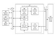
- FIG. 1illustrates a computing system 100 , in accordance with an embodiment of the present invention.
- the computing system 100includes a host processor 135 and a nonvolatile memory system 105 coupled to the host processor 135 .
- the nonvolatile memory system 105includes a nonvolatile memory controller 110 and a nonvolatile memory storage module 115 coupled to the nonvolatile memory controller 110 .
- the nonvolatile memory system 105may be a solid stated drive (SSD).
- the nonvolatile memory controller 110may include a processing module 120 , an error correction and detection module 125 , an interface module 150 and a redundant array of independent disks (RAID) control module 145 .
- the processing module 120may be coupled to the error correction and detection module 125 , the interface module 150 and the RAID control module 145 through a communication bus 155 , as is commonly know in the art.
- the error correction and detection module 125may be coupled to the communication bus 155 and to the nonvolatile memory storage module through a plurality of corresponding data channels 140 .
- the RAID control module 145may be coupled to the nonvolatile memory storage module through the corresponding data channels 140 and to the communication bus 155 .
- the nonvolatile memory storage module 115may include a plurality of nonvolatile memory storage chips 130 comprising a plurality of memory storage cells.
- the memory storage chips 130may be organized in pages, each comprising a plurality of memory storage cells.
- the nonvolatile memory storage module 115may be based on NAND technology and may include 512 NAND memory storage chips 130 to provide a total storage capacity of 1 TBytes.
- a 32-data channel 140 configurationmay be implemented to operate the 512 NAND memory storage chips 130 of the nonvolatile memory storage module 115 with the nonvolatile memory storage controller 110 using 16 independent channels.
- the interface module 150may receive one or more data write commands, and associated data, from the host processor 135 .
- the interface module 150may then communicate the data write commands to the error detection and correction module 125 .
- the error detection and correction module 125may encode the data prior to writing the data to the nonvolatile memory storage module.
- the datamay be encoded using an outer error correction code concatenated with an inner error correction code.
- the interface module 150may receive one or more data read commands from the host processor 135 .
- the interface module 150may then communicate the data read commands to the processing module 120 to instruct the error detection and correction module 125 to read the encoded data from the nonvolatile memory storage module 115 over one of the communication channels 140 .
- the error detection and correction module 125may then attempt to recover the data from the encoded data using the outer error correction code of the encoded data. If the data recovery is successful, the data may be recovered and the error detection and correction module 125 may communicate the data recovery to the processing module 120 .
- the error correction and detection module 125may attempt to recover the data from the encoded data by first using the inner error correction code and then using the outer error correction code. If the data recovery is successful using the inner error correction code followed by the outer error correction code, the data may be recovered and the error detection and correction module 125 may communicate the data recovery to the processing module 120 . If the data recovery fails when using the inner error correction followed by the outer error correction code, the error correction and detection module 125 may communicate the failure to the processing module 120 and the processing module 120 may instruct the RAID control module 145 to access the nonvolatile memory storage module 115 to recover the data from the encoded data stored in the nonvolatile memory storage module 115 .
- each of the processing module 120 , the error detection and correction module 125 , the interface module 150 , the RAID control module 145 and the nonvolatile memory storage module 115may include one or more hardware components, one or more software components, or some combination thereof.
- hardware componentsinclude a combinational logic circuit, a sequential logic circuit, a microprocessor, an embedded processor, an embedded controller, or the like.
- software componentsinclude a computing program, computing instructions, a software routine, or the like.
- the nonvolatile memory system 105is implemented in an integrated circuit of an integrated circuit device, which may include an integrated circuit package containing the integrated circuit. In some embodiments, the nonvolatile memory system 105 is implemented in a single integrated circuit die. In other embodiments, the nonvolatile memory system 105 is implemented in more than one integrated circuit die of an integrated circuit device which may include a multichip package containing the integrated circuit die.
- the nonvolatile memory controller 110is implemented in an integrated circuit of an integrated circuit device, which may include an integrated circuit package containing the integrated circuit. In some embodiments, the nonvolatile memory controller 110 is implemented in a single integrated circuit die. In other embodiments, the nonvolatile memory controller 110 is implemented in more than one integrated circuit die of an integrated circuit device which may include a multichip package containing the integrated circuit die.
- the nonvolatile memory storage module 115is implemented in an integrated circuit of an integrated circuit device, which may include an integrated circuit package containing the integrated circuit. In some embodiments, nonvolatile memory storage module 115 is implemented in a single integrated circuit die. In other embodiments, nonvolatile memory storage module 115 is implemented in more than one integrated circuit die of an integrated circuit device which may include a multichip package containing the integrated circuit die.
- FIG. 2illustrates the error correction and detection module 125 , in accordance with an embodiment of the present invention.
- the processing module 120 , the RAID control module 145 and the interface module 150may be coupled together though a communication bus 155 .
- the error detection and correction module 125may be coupled to the processing module 120 , the RAID control module 145 and the interface module 150 through the communication bus 155 .
- the error detection and correction module 125may be coupled to the nonvolatile memory storage module 115 through the communication bus 140 .
- the error detection and correction module 125may include an outer error correction code encoder 200 , an inner error correction code encoder 205 , an outer error correction code decoder 215 , an inner error correction code decoder 210 and an error detection module 220 .
- the terms “inner” and “outer”may reference the physical location and/or logical location of the encoders and decoders within the error detection and correction module relative to the nonvolatile memory storage module.
- the outer error correction code encoder 200may be coupled to the processing module 120 , the interface module 150 through the communication bus 155 .
- the inner error correction code encoder 205may be coupled to the outer error correction code encoder 200 and to the nonvolatile memory storage module 115 through the communication bus 140 .
- the inner error correction code decoder 210may be coupled to the nonvolatile memory storage module 115 through the communication bus 140 .
- the outer error correction code decoder 215may be coupled to the nonvolatile memory storage module 115 through the communication bus 140 , to the inner error correction code decoder 210 and to the error detection module 220 .
- the outer error correction code decoder 215may comprise the error detection module 220 .
- the outer error correction code decoder 215may further be coupled to the processing module 120 and the interface module 150 through the communication channel 155 .
- the error detection module 220may be coupled to the outer error correction code decoder 215 and to the processing module 120 , the RAID control module 145 and the interface module 150 through the communication channel 150 .
- the interface module 150may receive one or more data write commands, and associated data, from the host processor 135 .
- the interface module 150may then communicate the data write commands to the error detection and correction module 125 and to the processing module 120 through the communication bus 155 .
- the outer error correction code encoder 200 of the error detection and correction module 125may encode the data with an outer error correction code.
- the outer error correction code encoder 200may encode the data by adding redundant data, or parity bits, to the data, such that the data can be recovered from the nonvolatile memory storage module 115 when errors are subsequently introduced into the data by the nonvolatile memory storage module 115 .
- the error detection and correction modulemay subsequently read the encoded data from the nonvolatile memory storage module 115 , and the redundant data bits added to the data may allow the error detection and correction module 125 to determine whether or not the data stored in the nonvolatile memory storage module 115 has been corrupted during the storage of the data, and if so, the error detection and correction module 125 may identify the specific data bits that have been corrupted and correct the data.
- the outer error correction code encoder 200may add a number of parity bits to the data.
- the inner error correction code encoder 205may add additional parity bits to the data using an inner error correction code.
- the inner error correction codemay be a different error correction code than the outer error correction code.
- the inner error correction codemay exhibit an error floor.
- the datamay be encoded using an outer error correction code concatenated with an inner error correction code, wherein the outer error correction code applied to the data by the outer error correction code encoder 200 is concatenated with the inner error correction code applied to the data by the inner error correction code encoder 205 .
- the data comprising the outer error correction code concatenated with the inner error correction codemay then be written to the nonvolatile memory storage module 115 .
- the inner error correction code parity bitsare not included in the outer error correction code parity. Separating the parity of the inner error correction code from the parity of the outer error correction code allows the inner error correction code to be stored in a different flash page than the outer error correction code and the data.
- the inner error correction code in a specific implementationmay have a stronger error correction code than the outer error correction code. The stronger inner error correction code may result in a lower UBER at select RBERs. In addition, the stronger inner error correction code may result in an increased code rate for the inner error correction requiring a larger number of parity bits for encoding.
- the number of parity bits required for the inner error correction code ratemay be such that the data and the inner error correction code are unable to fit on the same flash page and it may be necessary to store the inner error correction code in a different flash page than the data.
- the outer error correction codemay be a weaker error correction code requiring fewer parity bits for encoding. As such, the outer error correction code may be able to fit on the same flash page as the data.
- the interface module 150may receive one or more data read commands from the host processor 135 . The interface module 150 may then communicate the data read commands to the processing module 120 to instruct the error detection and correction module 125 to read the encoded data from the nonvolatile memory storage module 125 over one of the communication channels 140 . In reading the encoded data from the nonvolatile memory storage module 125 , if the outer error correction code and the data encoded by the outer error correction code are stored on the same flash page, it may only be necessary for the error detection and correction module 125 to read the flash page that contains both the outer error correction code and the data.
- the encoded data read from the nonvolatile memory storage module 115may be received by the outer error correction code decoder 215 .
- the outer error correction code decoder 215may then attempt to recover the data from the encoded data by decoding the data using the outer error correction code of the encoded data.
- the outer error correction code decoder 215may then communicate with the error detection module 220 to determine if decoding the encoded data using the outer error correction code results in one or more decoding errors. In determining if one or more decoding errors are present in the decoded data, the error detection module 220 may use the redundant data bits that were added to the data by the outer error correction code encoder 200 to identify specific data bits that have been corrupted.
- the error detection module 220may also be used to determine if the number of decoding errors resulting from the decoding of the encoded data using the outer error correction code exceeds the correction capacity of the outer error correction code.
- the correction code capacity of the outer error correction code decoder 215will be exceeded if the number of errors is greater than the number of bits that the outer error correction code used by the outer error correction code decoder 215 is capable of correcting. If there are decoding errors in the data and the correction capacity of the outer error correction code is not exceeded, the outer error correction code decoder 215 may correct the error identified in the data. The corrected data may then be provided to the communication channel 155 . If the error detection module 220 does not identify any errors in the decoded data, the decoded data may be provided to the communication channel 155 without being corrected by the outer error correction code decoder 215 .
- the error correction and detection module 125may attempt to recover the data from the encoded data by first using the inner error correction code decoder 210 and then using the outer error correction code decoder 215 .
- the processing module 120may instruct the inner error correction code decoder 210 to read the encoded data from the nonvolatile memory storage module 115 .
- the error detection and correction module 125may read a first flash page that contains the outer error correction code and the data and to read a second flash page that contains the inner error correction code.
- the encoded data read from the nonvolatile memory storage module 115may be received by the outer error correction code decoder 215 .
- the inner error correction code decoder 210may then decode the data using the inner error correction code.
- the inner error correction code decoder 210may then determine if there are one or more errors in the decoded data and if it is determined that one or more errors exist in the decoded data, the inner error correction code decoder may correct the identified errors. In determining if one or more decoding errors are present in the decoded data, the inner error correction code decoder 210 may use the redundant data bits that were added to the data by the inner error correction code encoder 205 to identify specific data bits that have been corrupted. After any errors in the encoded data have been corrected by the inner error correction code decoder 210 , the corrected data may be communicated to the outer error correction code decoder 215 .
- the error detection module 220may be used to determine if the corrected data from the inner error correction code decoder 210 is in fact free of errors. It is possible for the inner error correction code decoder 210 to determine that the data has been successfully decoded, when in fact errors may still be present in the data corrected by the inner error correction code decoder 210 . In this case, the error detection module 220 may identify the errors that have not been successfully corrected by the inner error correction code decoder 210 . In a particular embodiment, the outer error correction code decoder 215 may comprise the error detection module 220 .
- the outer error correction code decoder 215may then attempt to recover the data from the encoded data by decoding the data corrected by the inner error correction code decoder 210 using the outer error correction code of the encoded data.
- the outer error correction code decoder 215may then communicate with the error detection module 220 to determine if decoding the data corrected by the inner error correction code decoder 210 using the outer error correction code results in one or more decoding errors. In determining if one or more decoding errors are present in the decoded data, the error detection module 220 may use the redundant data bits that were added to the data by the outer error correction code encoder 200 to identify specific data bits that have been corrupted.
- the error detection module 220may also be used to determine if the number of decoding errors resulting from the decoding of the data corrected by the inner error correction code decoder 210 using the outer error correction code exceeds the correction capacity of the outer error correction code decoder 215 .
- the correction code capacity of the outer error correction code decoder 215will be exceeded if the number or error is greater than the number of bits that the outer error correction code used by the outer error correction code decoder 215 is capable of correcting. If there are decoding errors in the corrected data and the correction capacity of the outer error correction code is not exceeded, the outer error correction code decoder 215 may correct the errors identified in the data. The corrected data may then be provided to the communication channel 155 . If the error detection module 220 does not identify any errors in the decoded data, the decoded data may be provided to the communication channel 155 without being further corrected by the outer error correction code decoder 215 .
- the error detection module 220may communicate to the processing module that the error detection and correction module 125 is unable to recover the data.
- the error detection module 220may communicate the failure to the processing module 120 and the processing module 120 may instruct the RAID control module 145 to access the nonvolatile memory storage module 115 to recover the data from the encoded data stored in the nonvolatile memory storage module 115 .
- the inner error correction code module 210 and the outer error correction code module 215are capable of correcting up to a maximum number of data bit errors in a data unit.
- the error correction capacity of the inner error correction code module 210 and the outer error correction code module 215is equal to the maximum number of data bit errors correctable in a data unit by the inner error correction code module 210 and the outer error correction code module 215 .
- the inner error correction code module 210 and the outer error correction code module 215are programmable to select an error correction capacity of the inner error correction code module 210 and the outer error correction code module 215 for correcting up to the maximum number of data bit errors correctable in a data unit by the inner error correction code module 210 and the outer error correction code module 215 .
- the selected error correction capacitymay be less than the maximum number of data bit errors correctable in a data unit by the inner error correction code module 210 and the outer error correction code module 215 .
- each of the outer error correction code encoder 200 , the inner error correction code encoder 205 , the inner error correction decoder 210 , the outer error correction code decoder 215 and the error detection module 220may include one or more hardware components, one or more software components, or some combination thereof.
- hardware componentsinclude a combinational logic circuit, a sequential logic circuit, a microprocessor, an embedded processor, an embedded controller, or the like.
- software componentsinclude a computing program, computing instructions, a software routine, or the like.
- the inner error correction codemay be a low-density parity check (LDPC) error correction code and the outer error correction code may be a Bose-Chaudhuri-Hochquenghem (BCH) error correction code.
- LDPClow-density parity check
- BCHBose-Chaudhuri-Hochquenghem
- the LDPC codemay selected from one of a variety of error correction codes associated with LDPC codes, including regular or irregular LDPC codes, quasi-cyclic LDPC codes, irregular repeat accumulate (IRA) codes, codes based on projective geometry or any of a variety of error correction codes associated with LDPC as are known in the art.
- the LDPC correction codemay be known to exhibit an error floor.
- the BCH error correction codemay have a very high error correction capacity.
- the BCH correction codemay have an uncorrected bit error rate (UBER) of 1 ⁇ 10 ⁇ 9 for a raw bit error rate (BER) of 1 ⁇ 10 ⁇ 3 .
- the BCH error correction codemay have an uncorrected bit error rate (UBER) of 1 ⁇ 10 ⁇ 12 for a raw bit error rate (BER) of 1 ⁇ 10 ⁇ 3 .
- the BCH error correction codemay have an uncorrected bit error rate (UBER) in the range of 1 ⁇ 10 ⁇ 9 to 1 ⁇ 10 ⁇ 15 for a raw bit error rate (BER) of 1 ⁇ 10 ⁇ 3 .
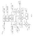
- FIG. 3is a diagram illustrating the flow of encoded data having an inner LDPC code concatenated with an outer BCH code, in accordance with an embodiment of the present invention.
- data 305is received at a BCH encoder 320 .
- the BCH encoderencodes the received data 305 by adding redundant bits 310 to the data 305 .
- the number of bits added to the datais dependent upon the BCH code being used. As is known in the art, a “strong” BCH code would add more redundant bits to the data than a “weak” BCH code.
- the data 305 and BCH code 310are then communicated to the LDPC encoder 325 .
- the LDPC encoder 325encodes the data 305 by adding redundant bits 315 to the data 305 .
- the datais encoded using a concatenated code including a BCH code 310 and an LDPC code 325 by adding the BCH code 310 and the LDPC code 325 to the data 305 to form the encoded data.
- a concatenated code including a BCH code 310 and an LDPC code 325by adding the BCH code 310 and the LDPC code 325 to the data 305 to form the encoded data.
- the data 305 , the BCH code 310 and the LDPC code 315may be stored in the same flash page.
- the encoded datacomprising the data 305 and the concatenated error codes 310 , 315 are then communicated to the nonvolatile memory storage module 330 .
- the encoded datais stored in the nonvolatile memory storage module 330 until the nonvolatile memory system 300 receives a read request.
- the nonvolatile memory system 300Upon receiving a read request at the nonvolatile memory system 300 , the nonvolatile memory system 300 reads the encoded data from the nonvolatile memory storage module 330 and communicates the encoded data, including the data 305 and the BCH code 310 , to the BCH decoder 335 . If the data 305 and the BCH code 310 are stored in the same flash page, it may only be necessary to read one flash page from the nonvolatile memory storage module 330 . The BCH decoder 335 will attempt to recover the data 305 from the encoded data using the BCH code 310 . The BCH decoder 335 recovers the data 305 from the encoded data by identifying any errors in the data using the BCH code 310 and correcting any identified errors.
- the BCH decoder 335is only able to correct the number of errors up to the correction capacity of the BCH code 310 . If the error correction capacity of the BCH decoder 335 is not exceeded, the BCH decoder 335 will be successful and the BCH decoder 335 will be able to recover the data 305 from the encoded data. If the error correction capacity of the BCH decoder 335 is exceeded and the BCH decoder 335 is unable to recover the data from the encoded data, the BCH decoder 335 recovery will fail 350 .
- the nonvolatile memory system 300communicates the encoded data, including the data 305 , the BCH code 310 and the LDPC code 315 , to the LDPC decoder 340 . If the data 305 and the BCH code 310 are stored in the same flash page, but the LDPC code 315 is stored in a different flash page, it may be necessary to read a first flash page containing the data 305 and the BCH code 310 and to read a second flash page containing the LDPC code 315 from the nonvolatile memory storage module 330 .
- the data 305 , the BCH code 310 and the LDPC code 315may be stored in the same flash page.
- the LDPC decoder 340will recover the data 305 from the encoded data using the LDPC code 315 .
- the LDPC decoder 340recovers the data 305 from the encoded data by identifying any errors in the data using the LDPC code 315 and correcting any identified errors.
- the data 305 and the BCH code 310are communicated to the BCH decoder 335 .
- the BCH decoder 335will attempt to recover the data 305 from the encoded data corrected by the LDPC decoder 340 using the BCH code 310 .
- the BCH decoder 335recovers the data 305 from the corrected data by identifying any remaining errors in the data using the BCH code 310 and correcting any identified errors. However, the BCH decoder 335 is only able to correct the number of errors up to the correction capacity of the BCH code 310 . If the error correction capacity of the BCH decoder 335 is not exceeded, the BCH decoder 335 will be successful and the BCH decoder 335 will be able to recover the data 305 from the data corrected by the LDPC decoder 340 . If the error correction capacity of the BCH decoder 335 is exceeded and the BCH decoder 335 is unable to recover the data from data corrected by the LDPC decoder 340 , the BCH decoder 335 recovery will fail 355 .
- the nonvolatile memory systemfails to recover the data 305 from the encoded data using the LDPC decoder 340 followed by the BCH decoder 335 , the nonvolatile memory system will communicate the read request to a redundant array of independent disks (RAID) module to recover the data 305 .
- RAIDredundant array of independent disks
- a RAID algorithmmay be performed by the RAID control module 345 on a standard RAID level (e.g., a RAID level 3-6), as is known in the relevant art.
- the data 305 and the BCH code 310may be communicated to the BCH decoder 335 .
- the BCH decoder 335will attempt to recover the data 305 from the encoded data corrected by the LDPC decoder 340 using the BCH code 310 .
- the BCH decoder 335recovers the data 305 from the corrected data by identifying any remaining errors in the data using the BCH code 310 and correcting any identified errors. In identifying any remaining errors in the data, the BCH decoder 335 may calculate the syndromes of the data 305 decoded by the LDPC decoder 340 .
- the BCH decoder 335may then determine if the calculated syndromes are non-zero or all zeros 360 . If it is determined that the syndromes are non-zero, then it can be established that the data 305 decoded by the LDPC decoder 340 has not been successfully recovered. In this case, the LDPC decoder 340 may determine that the data has been successfully recovered when in fact the data still contains errors. If it is determined that the BCH syndromes are non-zero 360 , the data 305 may be sent to the BCH decoder 335 for further decoding.
- the data 305may be sent directly to the redundant array of independent disks (RAID) module to recover the data 305 .
- RAIDredundant array of independent disks
- a RAID algorithmmay be performed by the RAID control module 345 on a standard RAID level (e.g., a RAID level 3-6), as is known in the relevant art.
- FIG. 4illustrates a flow diagram 400 for a method of recovering encoded data in a nonvolatile memory controller in accordance with an embodiment of the present invention.
- the nonvolatile memory controllerupon receiving a read request for data stored in a nonvolatile memory storage module, the nonvolatile memory controller initiates a request to read the concatenation encoded data stored in the nonvolatile memory storage module 405 .
- the concatenation encoded data stored in the nonvolatile memory storage modulemay include data having an outer error correction code concatenated with an inner error correction code.
- the outer error correction code and the inner error correction codemay be stored in the same flash page as the data.
- the outer error correction code and the datamay be stored in a first flash page and the inner error correction code may be stored in a second flash page.
- the concatenation encoded data stored in the nonvolatile memory storage modulemay include an LDPC code as an inner error correction code and a BCH code as an outer error correction code.
- the nonvolatile memory controllermay recover the data from the concatenation encoded data by decoding the concatenation encoded data using the outer error correction code 410 .
- the nonvolatile memory storage modulemay decode the data using the outer error correction code and then determine if there are any errors resulting from the decoding of the concatenation encoded data using the outer error correction code 415 .
- the datamay be recovered without being corrected and the nonvolatile memory controller may transfer the recovered data to a host processor.
- the nonvolatile memory storage controllermay then determine if the number of errors resulting from decoding the concatenation encoded data using the outer error correction code exceeds the correction capacity of the outer error correction code 420 .
- the correction capacity of the outer error correction codemay be exceeded if the number of errors resulting from the decoding of the concatenation encoded data using the outer error correction code is greater than the number of errors correctable by the outer error correction code.
- the data errorsmay be corrected using the outer error correction code 425 to successfully recover the data from the concatenated encoded data and the nonvolatile memory controller may transfer the recovered data to a host processor.
- the nonvolatile memory controllermay attempt to recover the data from the concatenated encoded data using the inner error correction code and the outer error correction code.
- the concatenation encoded datamay first be decoded using the inner error correction code 430 . Any errors detected during the decoding of the concatenation encoded data using the inner error correction code may be corrected using the inner error correction code 435 . After the concatenation encoded data has been decoded and corrected using the inner error correction code, the detection over the data that has been corrected using the inner error correction code may be computed 440 using the outer error correction code decoder.
- the computed detection over the data corrected using the inner error correction code 440indicates that the detection has failed 445 then it may be concluded that the data decoded by the inner error correction code decoder has not been successfully recovered and that the inner error correction code decoder has incorrectly determined that the data has been successfully recovered when in fact the data still contains errors. If the detection fails 445 , the data may be decoded using the outer error correction code decoder 450 if the correction capacity of the outer error correction code capacity has not been exceeded 452 . Alternatively, if the detection fails 445 , a redundant array of independent disks (RAID) operation 460 may be performed to recover the data.
- RAIDredundant array of independent disks
- the data errorsmay be corrected using the outer error correction code 455 to successfully recover the data from the concatenated encoded data and the nonvolatile memory controller may transfer the recovered data to a host processor.
- the nonvolatile memory controllermay communicate the read request to a redundant array of independent disks (RAID) control module to perform a RAID operation 460 for the read request to recover the data from the nonvolatile memory storage module.
- RAIDredundant array of independent disks
- the syndromes of the corrected datamay be calculated using the outer error correction code 440 . If the syndromes of the corrected data are non-zero, then the nonvolatile memory controller may communicate the read request to a redundant array of independent disks (RAID) control module to perform a RAID operation 460 for the read request to recover the data from the nonvolatile memory storage module.
- RAIDredundant array of independent disks
- the inner error correction code in combination with the outer correction codemay be used to improve the reliability of the nonvolatile memory system. While the inner error correction code may exhibit an error floor, the inner error correction code may be used to correct the data, thereby reducing the number of errors in the data before using the outer error correction code to correct the data. The outer correction code may then be used to meet the target UBER in the presence of the error floor of the inner error correction code.
- the method of the present inventionallows a target uncorrectable bit error rate (UBER) to be reached for a nonvolatile memory storage system in which the data exhibits a high raw bit error rate (RBER) in the range of an error floor in the correction code.
- UBERuncorrectable bit error rate
- RBERraw bit error rate
- the LDPC decoderis removed from the main data path to improve the overall performance of the nonvolatile memory system.
- the LDPC decoderis removed from the main data path to improve the overall performance of the nonvolatile memory system.
- removing the LDPC decoder from the main data patheliminates the need for multiple LDPC decoders in the system without sacrificing the performance of the system.
- the error rate of the nonvolatile storage systemtypically increases.
- the LDPC decoderis only used when the error rates are so high that they exceed the correctability of the BCH code, which typically begins to occur toward the end of life of the device.
- the LDPC decodermay be removed from the main data path, resulting in the ability to design a smaller, lower bandwidth, and lower power LDPC decoder.
- LDPCis able to correct data with a very high number of errors using fewer parity bits than other codes known in the art and can perform corrections with error rates that exceed the capability of most other codes.
- the code rates required to implement LDPCmay require that the LDPC code be stored in a separate flash page from the data it is encoding.
- the BCH code ratemay be small enough to be able to store the BCH parity in the same flash page as the data. While the smaller code rate for the BCH code may result in a less robust code than desired, the LDPC encoder can be implemented to overcome the weakness in the BCH code.
- the system performanceis improved because only one flash page needs to be read to decode the data.
- the software/firmware of the nonvolatile memory systemcan be simplified by eliminating the need to coordinate the complex interactions of the system when the BCH parity is stored on a different flash page than the data.
Landscapes
- Engineering & Computer Science (AREA)
- Theoretical Computer Science (AREA)
- Physics & Mathematics (AREA)
- Quality & Reliability (AREA)
- General Engineering & Computer Science (AREA)
- General Physics & Mathematics (AREA)
- Probability & Statistics with Applications (AREA)
- Techniques For Improving Reliability Of Storages (AREA)
Abstract
Description
Claims (25)
Priority Applications (1)
| Application Number | Priority Date | Filing Date | Title |
|---|---|---|---|
| US13/434,770US8656257B1 (en) | 2012-01-11 | 2012-03-29 | Nonvolatile memory controller with concatenated error correction codes |
Applications Claiming Priority (2)
| Application Number | Priority Date | Filing Date | Title |
|---|---|---|---|
| US201261585627P | 2012-01-11 | 2012-01-11 | |
| US13/434,770US8656257B1 (en) | 2012-01-11 | 2012-03-29 | Nonvolatile memory controller with concatenated error correction codes |
Publications (1)
| Publication Number | Publication Date |
|---|---|
| US8656257B1true US8656257B1 (en) | 2014-02-18 |
Family
ID=49776233
Family Applications (2)
| Application Number | Title | Priority Date | Filing Date |
|---|---|---|---|
| US13/434,770Active2032-07-10US8656257B1 (en) | 2012-01-11 | 2012-03-29 | Nonvolatile memory controller with concatenated error correction codes |
| US13/435,572Active2032-06-07US8621318B1 (en) | 2012-01-11 | 2012-03-30 | Nonvolatile memory controller with error detection for concatenated error correction codes |
Family Applications After (1)
| Application Number | Title | Priority Date | Filing Date |
|---|---|---|---|
| US13/435,572Active2032-06-07US8621318B1 (en) | 2012-01-11 | 2012-03-30 | Nonvolatile memory controller with error detection for concatenated error correction codes |
Country Status (1)
| Country | Link |
|---|---|
| US (2) | US8656257B1 (en) |
Cited By (46)
| Publication number | Priority date | Publication date | Assignee | Title |
|---|---|---|---|---|
| US8935598B1 (en) | 2013-03-12 | 2015-01-13 | Pmc-Sierra Us, Inc. | System and method for adaptive check node approximation in LDPC decoding |
| US8984376B1 (en) | 2013-03-14 | 2015-03-17 | Pmc-Sierra Us, Inc. | System and method for avoiding error mechanisms in layered iterative decoding |
| US8984365B1 (en) | 2013-03-14 | 2015-03-17 | Pmc-Sierra Us, Inc. | System and method for reduced memory storage in LDPC decoding |
| US20150082124A1 (en)* | 2013-09-19 | 2015-03-19 | Lsi Corporation | Spatially decoupled redundancy schemes for a solid state drive (ssd) |
| US8990661B1 (en) | 2013-03-05 | 2015-03-24 | Pmc-Sierra Us, Inc. | Layer specific attenuation factor LDPC decoder |
| US8995302B1 (en) | 2013-01-16 | 2015-03-31 | Pmc-Sierra Us, Inc. | Method and apparatus for translated routing in an interconnect switch |
| US20150186210A1 (en)* | 2013-12-30 | 2015-07-02 | Silicon Motion Inc. | Method for performing error correction, associated memory apparatus and associated controller thereof |
| US9092353B1 (en) | 2013-01-29 | 2015-07-28 | Pmc-Sierra Us, Inc. | Apparatus and method based on LDPC codes for adjusting a correctable raw bit error rate limit in a memory system |
| US9128858B1 (en) | 2013-01-29 | 2015-09-08 | Pmc-Sierra Us, Inc. | Apparatus and method for adjusting a correctable raw bit error rate limit in a memory system using strong log-likelihood (LLR) values |
| US9235467B2 (en) | 2013-03-15 | 2016-01-12 | Pmc-Sierra Us, Inc. | System and method with reference voltage partitioning for low density parity check decoding |
| US9397701B1 (en) | 2013-03-11 | 2016-07-19 | Microsemi Storage Solutions (Us), Inc. | System and method for lifetime specific LDPC decoding |
| US9417804B2 (en) | 2014-07-07 | 2016-08-16 | Microsemi Storage Solutions (Us), Inc. | System and method for memory block pool wear leveling |
| US9450610B1 (en) | 2013-03-15 | 2016-09-20 | Microsemi Storage Solutions (Us), Inc. | High quality log likelihood ratios determined using two-index look-up table |
| US9454414B2 (en) | 2013-03-15 | 2016-09-27 | Microsemi Storage Solutions (Us), Inc. | System and method for accumulating soft information in LDPC decoding |
| US9520185B2 (en) | 2010-04-19 | 2016-12-13 | Silicon Motion Inc. | Method for performing memory access management, and associated memory device and controller thereof |
| US9590656B2 (en) | 2013-03-15 | 2017-03-07 | Microsemi Storage Solutions (Us), Inc. | System and method for higher quality log likelihood ratios in LDPC decoding |
| US9684559B1 (en) | 2014-04-25 | 2017-06-20 | Altera Corporation | Methods and apparatus for storing error correction information on a memory controller circuit |
| US9799405B1 (en) | 2015-07-29 | 2017-10-24 | Ip Gem Group, Llc | Nonvolatile memory system with read circuit for performing reads using threshold voltage shift read instruction |
| US9813080B1 (en) | 2013-03-05 | 2017-11-07 | Microsemi Solutions (U.S.), Inc. | Layer specific LDPC decoder |
| US9886214B2 (en) | 2015-12-11 | 2018-02-06 | Ip Gem Group, Llc | Nonvolatile memory system with erase suspend circuit and method for erase suspend management |
| US9892794B2 (en) | 2016-01-04 | 2018-02-13 | Ip Gem Group, Llc | Method and apparatus with program suspend using test mode |
| US9899092B2 (en) | 2016-01-27 | 2018-02-20 | Ip Gem Group, Llc | Nonvolatile memory system with program step manager and method for program step management |
| US10157677B2 (en) | 2016-07-28 | 2018-12-18 | Ip Gem Group, Llc | Background reference positioning and local reference positioning using threshold voltage shift read |
| US10180875B2 (en) | 2016-07-08 | 2019-01-15 | Toshiba Memory Corporation | Pool-level solid state drive error correction |
| US10230396B1 (en) | 2013-03-05 | 2019-03-12 | Microsemi Solutions (Us), Inc. | Method and apparatus for layer-specific LDPC decoding |
| US10236915B2 (en) | 2016-07-29 | 2019-03-19 | Microsemi Solutions (U.S.), Inc. | Variable T BCH encoding |
| US10275311B2 (en) | 2016-02-03 | 2019-04-30 | Samsung Electronics Co., Ltd. | Raid-6 data storage device and data processing system including the same |
| US10291263B2 (en) | 2016-07-28 | 2019-05-14 | Ip Gem Group, Llc | Auto-learning log likelihood ratio |
| US10332613B1 (en) | 2015-05-18 | 2019-06-25 | Microsemi Solutions (Us), Inc. | Nonvolatile memory system with retention monitor |
| WO2019204017A1 (en) | 2018-04-20 | 2019-10-24 | Micron Technology, Inc. | Error correction using hierarchical decoders |
| US10467094B2 (en) | 2016-03-04 | 2019-11-05 | Samsung Electronics Co., Ltd. | Method and apparatus for performing data recovery in a raid storage |
| WO2020036752A1 (en)* | 2018-08-17 | 2020-02-20 | Micron Technology, Inc. | Enhanced bit flipping scheme |
| US11016689B2 (en) | 2016-09-27 | 2021-05-25 | Samsung Electronics Co., Ltd. | Data storage system |
| US11086716B2 (en) | 2019-07-24 | 2021-08-10 | Microchip Technology Inc. | Memory controller and method for decoding memory devices with early hard-decode exit |
| US11398291B2 (en) | 2020-11-20 | 2022-07-26 | Microchip Technology Inc. | Method and apparatus for determining when actual wear of a flash memory device differs from reliability states for the flash memory device |
| US11514994B1 (en) | 2021-05-28 | 2022-11-29 | Microchip Technology Inc. | Method and apparatus for outlier management |
| US11514992B2 (en) | 2021-02-25 | 2022-11-29 | Microchip Technology Inc. | Method and apparatus for reading a flash memory device |
| US11663076B2 (en) | 2021-06-01 | 2023-05-30 | Microchip Technology Inc. | Memory address protection |
| US20230176947A1 (en)* | 2021-12-08 | 2023-06-08 | Western Digital Technologies, Inc. | Memory matched low density parity check coding schemes |
| US11699493B2 (en) | 2021-05-24 | 2023-07-11 | Microchip Technology Inc. | Method and apparatus for performing a read of a flash memory using predicted retention-and-read-disturb-compensated threshold voltage shift offset values |
| US11843393B2 (en) | 2021-09-28 | 2023-12-12 | Microchip Technology Inc. | Method and apparatus for decoding with trapped-block management |
| US11869584B2 (en) | 2010-04-19 | 2024-01-09 | Silicon Motion, Inc. | Memory access module for performing a plurality of sensing operations to generate digital values of a storage cell in order to perform decoding of the storage cell |
| US11934696B2 (en) | 2021-05-18 | 2024-03-19 | Microchip Technology Inc. | Machine learning assisted quality of service (QoS) for solid state drives |
| US12175363B2 (en) | 2020-07-27 | 2024-12-24 | Microchip Technology Inc. | Regression neural network for identifying threshold voltages to be used in reads of flash memory devices |
| US12393846B2 (en) | 2020-08-20 | 2025-08-19 | Microchip Technology Inc. | Partitionable neural network for solid state drives |
| US12401377B2 (en) | 2023-12-14 | 2025-08-26 | SK Hynix Inc. | Error correction based on asymmetric ratio |
Families Citing this family (47)
| Publication number | Priority date | Publication date | Assignee | Title |
|---|---|---|---|---|
| US8972824B1 (en) | 2012-05-22 | 2015-03-03 | Pmc-Sierra, Inc. | Systems and methods for transparently varying error correction code strength in a flash drive |
| US9183085B1 (en) | 2012-05-22 | 2015-11-10 | Pmc-Sierra, Inc. | Systems and methods for adaptively selecting from among a plurality of error correction coding schemes in a flash drive for robustness and low latency |
| US8788910B1 (en)* | 2012-05-22 | 2014-07-22 | Pmc-Sierra, Inc. | Systems and methods for low latency, high reliability error correction in a flash drive |
| US9176812B1 (en) | 2012-05-22 | 2015-11-03 | Pmc-Sierra, Inc. | Systems and methods for storing data in page stripes of a flash drive |
| US8996957B1 (en) | 2012-05-22 | 2015-03-31 | Pmc-Sierra, Inc. | Systems and methods for initializing regions of a flash drive having diverse error correction coding (ECC) schemes |
| US9021333B1 (en) | 2012-05-22 | 2015-04-28 | Pmc-Sierra, Inc. | Systems and methods for recovering data from failed portions of a flash drive |
| US8793556B1 (en) | 2012-05-22 | 2014-07-29 | Pmc-Sierra, Inc. | Systems and methods for reclaiming flash blocks of a flash drive |
| US9047214B1 (en) | 2012-05-22 | 2015-06-02 | Pmc-Sierra, Inc. | System and method for tolerating a failed page in a flash device |
| US9065483B2 (en)* | 2013-01-21 | 2015-06-23 | Micron Technology, Inc. | Determining soft data using a classification code |
| US9208018B1 (en) | 2013-03-15 | 2015-12-08 | Pmc-Sierra, Inc. | Systems and methods for reclaiming memory for solid-state memory |
| US9009565B1 (en) | 2013-03-15 | 2015-04-14 | Pmc-Sierra, Inc. | Systems and methods for mapping for solid-state memory |
| US9053012B1 (en) | 2013-03-15 | 2015-06-09 | Pmc-Sierra, Inc. | Systems and methods for storing data for solid-state memory |
| US9081701B1 (en) | 2013-03-15 | 2015-07-14 | Pmc-Sierra, Inc. | Systems and methods for decoding data for solid-state memory |
| US9026867B1 (en) | 2013-03-15 | 2015-05-05 | Pmc-Sierra, Inc. | Systems and methods for adapting to changing characteristics of multi-level cells in solid-state memory |
| KR102110767B1 (en)* | 2013-12-24 | 2020-06-09 | 삼성전자 주식회사 | Operating method of memory controller and the memory controller |
| US9595352B2 (en) | 2014-03-17 | 2017-03-14 | Seagate Technology Llc | Manufacturer self-test for solid-state drives |
| US20150317204A1 (en)* | 2014-04-30 | 2015-11-05 | Lsi Corporation | Systems and Methods for Efficient Data Refresh in a Storage Device |
| US10608784B2 (en) | 2016-03-15 | 2020-03-31 | ClineHair Commercial Endeavors | Distributed storage system data management and security |
| US9405624B2 (en) | 2014-06-19 | 2016-08-02 | Seagate Technology Llc | On-die error detection and correction during multi-step programming |
| US10089177B2 (en)* | 2014-06-30 | 2018-10-02 | Sandisk Technologies Llc | Multi-stage decoder |
| US9407294B2 (en)* | 2014-07-07 | 2016-08-02 | Kabushi Kaisha Toshiba. | Non-volatile memory controller with error correction (ECC) tuning via error statistics collection |
| US9524207B2 (en) | 2014-09-02 | 2016-12-20 | Micron Technology, Inc. | Lee metric error correcting code |
| US9654144B2 (en) | 2014-09-30 | 2017-05-16 | Micron Technology, Inc. | Progressive effort decoder architecture |
| KR102275717B1 (en)* | 2015-01-21 | 2021-07-09 | 에스케이하이닉스 주식회사 | Flash memory system and operating method thereof |
| US20160266972A1 (en)* | 2015-03-10 | 2016-09-15 | Kabushiki Kaisha Toshiba | Memory controller, storage device and decoding method |
| US20160378591A1 (en)* | 2015-06-24 | 2016-12-29 | Intel Corporation | Adaptive error correction in memory devices |
| US10133625B2 (en) | 2015-08-11 | 2018-11-20 | Western Digital Technologies, Inc. | Storing parity data separate from protected data |
| KR102385138B1 (en) | 2015-10-08 | 2022-04-12 | 삼성전자주식회사 | Raid controller device and storage device configured to recover data having uncorrectable ecc error |
| US10931402B2 (en) | 2016-03-15 | 2021-02-23 | Cloud Storage, Inc. | Distributed storage system data management and security |
| US10009043B2 (en)* | 2016-06-30 | 2018-06-26 | Intel Corporation | Technologies for providing efficient error correction with half product codes |
| US10025661B1 (en)* | 2016-12-27 | 2018-07-17 | Sandisk Technologies Llc | Adaptive hard and soft bit decoding |
| KR102396814B1 (en)* | 2017-05-02 | 2022-05-11 | 삼성전자 주식회사 | Apparatus and method for channel encoding/decoding in communication or broadcasting system |
| US10269422B2 (en)* | 2017-09-08 | 2019-04-23 | Cnex Labs, Inc. | Storage system with data reliability mechanism and method of operation thereof |
| TWI658363B (en)* | 2017-10-20 | 2019-05-01 | 慧榮科技股份有限公司 | Storage device and interface chip thereof |
| US11070234B2 (en)* | 2018-03-16 | 2021-07-20 | SK Hynix Inc. | Memory system with hybrid decoding scheme with information exchange and method of operating such memory system |
| US11005503B2 (en) | 2018-03-16 | 2021-05-11 | SK Hynix Inc. | Memory system with hybrid decoding scheme and method of operating such memory system |
| US10884858B2 (en) | 2018-03-16 | 2021-01-05 | SK Hynix Inc. | LDPC decoding device, memory system including the same and method thereof |
| US11182247B2 (en) | 2019-01-29 | 2021-11-23 | Cloud Storage, Inc. | Encoding and storage node repairing method for minimum storage regenerating codes for distributed storage systems |
| US10977125B2 (en)* | 2019-06-06 | 2021-04-13 | Western Digital Technologies, Inc. | Adaptive usage of irregular code schemas based on specific system level triggers and policies |
| US11164652B2 (en) | 2019-06-21 | 2021-11-02 | Micron Technology, Inc. | Two-layer code with low parity cost for memory sub-systems |
| US11309915B1 (en) | 2019-07-11 | 2022-04-19 | Arrowhead Center, Inc. | Efficient implementation of a threshold modified min-sum algorithm for low-density parity-check decoders |
| US11296729B2 (en) | 2020-07-23 | 2022-04-05 | Micron Technology, Inc. | Data reliability for extreme temperature usage conditions in data storage |
| US11592994B2 (en)* | 2020-10-29 | 2023-02-28 | EMC IP Holding Company LLC | Providing preferential treatment to metadata over user data |
| US11368170B1 (en) | 2021-04-29 | 2022-06-21 | Marvell Asia Pte, Ltd. | Systems and methods for Nyquist error correction |
| KR20230049881A (en)* | 2021-10-07 | 2023-04-14 | 삼성전자주식회사 | Storage device and method of operating storage device |
| US12067239B2 (en)* | 2021-12-30 | 2024-08-20 | Micron Technology, Inc. | Data stripe protection |
| CN119645306A (en)* | 2024-11-28 | 2025-03-18 | 联和存储科技(江苏)有限公司 | NAND FLASH controller error correction method and device and flash memory |
Citations (7)
| Publication number | Priority date | Publication date | Assignee | Title |
|---|---|---|---|---|
| US6115788A (en)* | 1998-02-20 | 2000-09-05 | Seagate Technology, Inc. | Multi-drive array with improved data transfer rate performance |
| US20030225970A1 (en)* | 2002-05-28 | 2003-12-04 | Ebrahim Hashemi | Method and system for striping spares in a data storage system including an array of disk drives |
| US20040088636A1 (en)* | 2002-06-28 | 2004-05-06 | Cypher Robert E. | Error detection/correction code which detects and corrects a first failing component and optionally a second failing component |
| US6976194B2 (en)* | 2002-06-28 | 2005-12-13 | Sun Microsystems, Inc. | Memory/Transmission medium failure handling controller and method |
| US20100199149A1 (en) | 2007-12-05 | 2010-08-05 | Hanan Weingarten | Flash memory apparatus and methods using a plurality of decoding stages including optional use of concatenated bch codes and/or designation of "first below" cells |
| US20110246853A1 (en) | 2010-04-02 | 2011-10-06 | Yong-June Kim | Semiconductor device and decoding method thereof |
| US8255770B2 (en) | 2006-12-06 | 2012-08-28 | Samsung Electronics Co., Ltd. | Multi-level cell memory device and method thereof |
- 2012
- 2012-03-29USUS13/434,770patent/US8656257B1/enactiveActive
- 2012-03-30USUS13/435,572patent/US8621318B1/enactiveActive
Patent Citations (9)
| Publication number | Priority date | Publication date | Assignee | Title |
|---|---|---|---|---|
| US6115788A (en)* | 1998-02-20 | 2000-09-05 | Seagate Technology, Inc. | Multi-drive array with improved data transfer rate performance |
| US20030225970A1 (en)* | 2002-05-28 | 2003-12-04 | Ebrahim Hashemi | Method and system for striping spares in a data storage system including an array of disk drives |
| US6934804B2 (en)* | 2002-05-28 | 2005-08-23 | Sun Microsystems, Inc. | Method and system for striping spares in a data storage system including an array of disk drives |
| US20040088636A1 (en)* | 2002-06-28 | 2004-05-06 | Cypher Robert E. | Error detection/correction code which detects and corrects a first failing component and optionally a second failing component |
| US6976194B2 (en)* | 2002-06-28 | 2005-12-13 | Sun Microsystems, Inc. | Memory/Transmission medium failure handling controller and method |
| US8255770B2 (en) | 2006-12-06 | 2012-08-28 | Samsung Electronics Co., Ltd. | Multi-level cell memory device and method thereof |
| US20100199149A1 (en) | 2007-12-05 | 2010-08-05 | Hanan Weingarten | Flash memory apparatus and methods using a plurality of decoding stages including optional use of concatenated bch codes and/or designation of "first below" cells |
| US8335977B2 (en) | 2007-12-05 | 2012-12-18 | Densbits Technologies Ltd. | Flash memory apparatus and methods using a plurality of decoding stages including optional use of concatenated BCH codes and/or designation of “first below” cells |
| US20110246853A1 (en) | 2010-04-02 | 2011-10-06 | Yong-June Kim | Semiconductor device and decoding method thereof |
Cited By (68)
| Publication number | Priority date | Publication date | Assignee | Title |
|---|---|---|---|---|
| US10490268B2 (en) | 2010-04-19 | 2019-11-26 | Silicon Motion Inc. | Memory access module for performing memory access management |
| US10102904B2 (en) | 2010-04-19 | 2018-10-16 | Silicon Motion Inc. | Memory access module for performing a plurality of sensing operations to generate digital values of a storage cell in order to perform decoding of the storage cell |
| US11869584B2 (en) | 2010-04-19 | 2024-01-09 | Silicon Motion, Inc. | Memory access module for performing a plurality of sensing operations to generate digital values of a storage cell in order to perform decoding of the storage cell |
| US9858996B2 (en) | 2010-04-19 | 2018-01-02 | Silicon Motion Inc. | Memory access module for performing sensing operations on storage cells of a storage device to obtain soft information and executing a program mode to control access to the storage device |
| US11386952B2 (en) | 2010-04-19 | 2022-07-12 | Silicon Motion, Inc. | Memory access module for performing a plurality of sensing operations to generate digital values of a storage cell in order to perform decoding of the storage cell |
| US10854285B2 (en) | 2010-04-19 | 2020-12-01 | Silicon Motion, Inc. | Memory access module for performing a plurality of sensing operations to generate digital values of a storage cell in order to perform decoding of the storage cell |
| US12277966B2 (en) | 2010-04-19 | 2025-04-15 | Silicon Motion, Inc. | Memory access module for performing a plurality of sensing operations to generate digital values of a storage cell in order to perform decoding of the storage cell |
| US9627050B2 (en) | 2010-04-19 | 2017-04-18 | Silicon Motion Inc. | Memory access module for performing memory access management |
| US9520185B2 (en) | 2010-04-19 | 2016-12-13 | Silicon Motion Inc. | Method for performing memory access management, and associated memory device and controller thereof |
| US8995302B1 (en) | 2013-01-16 | 2015-03-31 | Pmc-Sierra Us, Inc. | Method and apparatus for translated routing in an interconnect switch |
| US9092353B1 (en) | 2013-01-29 | 2015-07-28 | Pmc-Sierra Us, Inc. | Apparatus and method based on LDPC codes for adjusting a correctable raw bit error rate limit in a memory system |
| US9448881B1 (en) | 2013-01-29 | 2016-09-20 | Microsemi Storage Solutions (Us), Inc. | Memory controller and integrated circuit device for correcting errors in data read from memory cells |
| US9128858B1 (en) | 2013-01-29 | 2015-09-08 | Pmc-Sierra Us, Inc. | Apparatus and method for adjusting a correctable raw bit error rate limit in a memory system using strong log-likelihood (LLR) values |
| US8990661B1 (en) | 2013-03-05 | 2015-03-24 | Pmc-Sierra Us, Inc. | Layer specific attenuation factor LDPC decoder |
| US10230396B1 (en) | 2013-03-05 | 2019-03-12 | Microsemi Solutions (Us), Inc. | Method and apparatus for layer-specific LDPC decoding |
| US9813080B1 (en) | 2013-03-05 | 2017-11-07 | Microsemi Solutions (U.S.), Inc. | Layer specific LDPC decoder |
| US9397701B1 (en) | 2013-03-11 | 2016-07-19 | Microsemi Storage Solutions (Us), Inc. | System and method for lifetime specific LDPC decoding |
| US8935598B1 (en) | 2013-03-12 | 2015-01-13 | Pmc-Sierra Us, Inc. | System and method for adaptive check node approximation in LDPC decoding |
| US8984376B1 (en) | 2013-03-14 | 2015-03-17 | Pmc-Sierra Us, Inc. | System and method for avoiding error mechanisms in layered iterative decoding |
| US8984365B1 (en) | 2013-03-14 | 2015-03-17 | Pmc-Sierra Us, Inc. | System and method for reduced memory storage in LDPC decoding |
| US9450610B1 (en) | 2013-03-15 | 2016-09-20 | Microsemi Storage Solutions (Us), Inc. | High quality log likelihood ratios determined using two-index look-up table |
| US9590656B2 (en) | 2013-03-15 | 2017-03-07 | Microsemi Storage Solutions (Us), Inc. | System and method for higher quality log likelihood ratios in LDPC decoding |
| US9235467B2 (en) | 2013-03-15 | 2016-01-12 | Pmc-Sierra Us, Inc. | System and method with reference voltage partitioning for low density parity check decoding |
| US9454414B2 (en) | 2013-03-15 | 2016-09-27 | Microsemi Storage Solutions (Us), Inc. | System and method for accumulating soft information in LDPC decoding |
| US20150082124A1 (en)* | 2013-09-19 | 2015-03-19 | Lsi Corporation | Spatially decoupled redundancy schemes for a solid state drive (ssd) |
| US9424131B2 (en)* | 2013-09-19 | 2016-08-23 | Avago Technologies General Ip (Singapore) Pte. Ltd. | Spatially decoupled redundancy schemes for a solid state drive (SSD) |
| US20150186210A1 (en)* | 2013-12-30 | 2015-07-02 | Silicon Motion Inc. | Method for performing error correction, associated memory apparatus and associated controller thereof |
| US9405619B2 (en)* | 2013-12-30 | 2016-08-02 | Silicon Motion Inc. | Method for performing error correction, associated memory apparatus and associated controller thereof |
| US9684559B1 (en) | 2014-04-25 | 2017-06-20 | Altera Corporation | Methods and apparatus for storing error correction information on a memory controller circuit |
| US9417804B2 (en) | 2014-07-07 | 2016-08-16 | Microsemi Storage Solutions (Us), Inc. | System and method for memory block pool wear leveling |
| US10332613B1 (en) | 2015-05-18 | 2019-06-25 | Microsemi Solutions (Us), Inc. | Nonvolatile memory system with retention monitor |
| US9799405B1 (en) | 2015-07-29 | 2017-10-24 | Ip Gem Group, Llc | Nonvolatile memory system with read circuit for performing reads using threshold voltage shift read instruction |
| US10152273B2 (en) | 2015-12-11 | 2018-12-11 | Ip Gem Group, Llc | Nonvolatile memory controller and method for erase suspend management that increments the number of program and erase cycles after erase suspend |
| US9886214B2 (en) | 2015-12-11 | 2018-02-06 | Ip Gem Group, Llc | Nonvolatile memory system with erase suspend circuit and method for erase suspend management |
| US9892794B2 (en) | 2016-01-04 | 2018-02-13 | Ip Gem Group, Llc | Method and apparatus with program suspend using test mode |
| US9899092B2 (en) | 2016-01-27 | 2018-02-20 | Ip Gem Group, Llc | Nonvolatile memory system with program step manager and method for program step management |
| US10275311B2 (en) | 2016-02-03 | 2019-04-30 | Samsung Electronics Co., Ltd. | Raid-6 data storage device and data processing system including the same |
| US10467094B2 (en) | 2016-03-04 | 2019-11-05 | Samsung Electronics Co., Ltd. | Method and apparatus for performing data recovery in a raid storage |
| US10180875B2 (en) | 2016-07-08 | 2019-01-15 | Toshiba Memory Corporation | Pool-level solid state drive error correction |
| US10740175B2 (en) | 2016-07-08 | 2020-08-11 | Toshiba Memory Corporation | Pool-level solid state drive error correction |
| US10283215B2 (en) | 2016-07-28 | 2019-05-07 | Ip Gem Group, Llc | Nonvolatile memory system with background reference positioning and local reference positioning |
| US10157677B2 (en) | 2016-07-28 | 2018-12-18 | Ip Gem Group, Llc | Background reference positioning and local reference positioning using threshold voltage shift read |
| US10291263B2 (en) | 2016-07-28 | 2019-05-14 | Ip Gem Group, Llc | Auto-learning log likelihood ratio |
| US10236915B2 (en) | 2016-07-29 | 2019-03-19 | Microsemi Solutions (U.S.), Inc. | Variable T BCH encoding |
| US11016689B2 (en) | 2016-09-27 | 2021-05-25 | Samsung Electronics Co., Ltd. | Data storage system |
| WO2019204017A1 (en) | 2018-04-20 | 2019-10-24 | Micron Technology, Inc. | Error correction using hierarchical decoders |
| US11237901B2 (en) | 2018-04-20 | 2022-02-01 | Micron Technology, Inc. | Error correction using hierarchical decoders |
| US11775383B2 (en) | 2018-08-17 | 2023-10-03 | Micron Technology, Inc. | Enhanced bit flipping scheme |
| TWI709035B (en)* | 2018-08-17 | 2020-11-01 | 美商美光科技公司 | Method and apparatus for operating bit flipping |
| KR20210034088A (en)* | 2018-08-17 | 2021-03-29 | 마이크론 테크놀로지, 인크 | Improved bit flipping method |
| US11256566B2 (en) | 2018-08-17 | 2022-02-22 | Micron Technology, Inc. | Enhanced bit flipping scheme |
| CN112543921B (en)* | 2018-08-17 | 2022-06-21 | 美光科技公司 | Enhanced Bit Flip Scheme |
| CN112543921A (en)* | 2018-08-17 | 2021-03-23 | 美光科技公司 | Reinforced position overturning scheme |
| US10802909B2 (en) | 2018-08-17 | 2020-10-13 | Micron Technology, Inc. | Enhanced bit flipping scheme |
| WO2020036752A1 (en)* | 2018-08-17 | 2020-02-20 | Micron Technology, Inc. | Enhanced bit flipping scheme |
| US11086716B2 (en) | 2019-07-24 | 2021-08-10 | Microchip Technology Inc. | Memory controller and method for decoding memory devices with early hard-decode exit |
| US12175363B2 (en) | 2020-07-27 | 2024-12-24 | Microchip Technology Inc. | Regression neural network for identifying threshold voltages to be used in reads of flash memory devices |
| US12393846B2 (en) | 2020-08-20 | 2025-08-19 | Microchip Technology Inc. | Partitionable neural network for solid state drives |
| US11398291B2 (en) | 2020-11-20 | 2022-07-26 | Microchip Technology Inc. | Method and apparatus for determining when actual wear of a flash memory device differs from reliability states for the flash memory device |
| US11514992B2 (en) | 2021-02-25 | 2022-11-29 | Microchip Technology Inc. | Method and apparatus for reading a flash memory device |
| US11934696B2 (en) | 2021-05-18 | 2024-03-19 | Microchip Technology Inc. | Machine learning assisted quality of service (QoS) for solid state drives |
| US11699493B2 (en) | 2021-05-24 | 2023-07-11 | Microchip Technology Inc. | Method and apparatus for performing a read of a flash memory using predicted retention-and-read-disturb-compensated threshold voltage shift offset values |
| US11514994B1 (en) | 2021-05-28 | 2022-11-29 | Microchip Technology Inc. | Method and apparatus for outlier management |
| US11663076B2 (en) | 2021-06-01 | 2023-05-30 | Microchip Technology Inc. | Memory address protection |
| US11843393B2 (en) | 2021-09-28 | 2023-12-12 | Microchip Technology Inc. | Method and apparatus for decoding with trapped-block management |
| US11860733B2 (en)* | 2021-12-08 | 2024-01-02 | Western Digital Technologies, Inc. | Memory matched low density parity check coding schemes |
| US20230176947A1 (en)* | 2021-12-08 | 2023-06-08 | Western Digital Technologies, Inc. | Memory matched low density parity check coding schemes |
| US12401377B2 (en) | 2023-12-14 | 2025-08-26 | SK Hynix Inc. | Error correction based on asymmetric ratio |
Also Published As
| Publication number | Publication date |
|---|---|
| US8621318B1 (en) | 2013-12-31 |
Similar Documents
| Publication | Publication Date | Title |
|---|---|---|
| US8656257B1 (en) | Nonvolatile memory controller with concatenated error correction codes | |
| US10135465B2 (en) | Error correction methods and apparatuses using first and second decoders | |
| KR101877106B1 (en) | Data reliability schemes for data storage systems | |
| CN104937555B (en) | Method and controller for controlling memory device and memory system | |
| US9319073B2 (en) | Mitigation of write errors in multi-level cell flash memory through adaptive error correction code decoding | |
| US8495471B2 (en) | Solid-state storage system with parallel access of multiple flash/PCM devices | |
| US8694849B1 (en) | Shuffler error correction code system and method | |
| CN105260258B (en) | Hierarchical ECC single-chip and dual-chip CHIPKILL solutions | |
| US8713411B2 (en) | Encoding and/or decoding memory devices and methods thereof | |
| US10326479B2 (en) | Apparatuses and methods for layer-by-layer error correction | |
| US11086716B2 (en) | Memory controller and method for decoding memory devices with early hard-decode exit | |
| US10447301B2 (en) | Optimal LDPC bit flip decision | |
| US20140026018A1 (en) | Method for reading data from block of flash memory and associated memory device | |
| CN106816179A (en) | A kind of flash error correction method and apparatus | |
| CN101256842A (en) | Error-correcting code controller and memory system including the error-correcting code controller | |
| CN103839594A (en) | Solid-state storage device and joint encoding and decoding method thereof | |
| US8856616B1 (en) | Two dimensional encoding for non-volatile memory blocks | |
| US20180203625A1 (en) | Storage system with multi-dimensional data protection mechanism and method of operation thereof | |
| US8756473B1 (en) | Solid state device coding architecture for chipkill and endurance improvement | |
| US20250265152A1 (en) | Semiconductor chip of correcting aligned error and semiconductor system of correcting aligned error |
Legal Events
| Date | Code | Title | Description |
|---|---|---|---|
| AS | Assignment | Owner name:INTEGRATED DEVICE TECHNOLOGY, INC., CALIFORNIA Free format text:ASSIGNMENT OF ASSIGNORS INTEREST;ASSIGNORS:MICHELONI, RINO;MARELLI, ALESSIA;ONUFRYK, PETER Z.;AND OTHERS;SIGNING DATES FROM 20120322 TO 20120329;REEL/FRAME:027959/0854 | |
| AS | Assignment | Owner name:INTEGRATED DEVICE TECHNOLOGY, INC., CALIFORNIA Free format text:ASSIGNMENT OF ASSIGNORS INTEREST;ASSIGNOR:PMC-SIERRA US, INC.;REEL/FRAME:030832/0604 Effective date:20130712 | |
| AS | Assignment | Owner name:PMC-SIERRA US, INC., CALIFORNIA Free format text:CORRECTIVE ASSIGNMENT TO CORRECT THE CONVEYING AND RECEIVING PARTIES PREVIOUSLY RECORDED ON REEL 030832 FRAME 0604. ASSIGNOR(S) HEREBY CONFIRMS THE CONVEYING PARTY DATA: INTEGRATED DEVICE TECHNOLOGY, INC. TECEIVING: PMC-SIERRA US, INC;ASSIGNOR:INTEGRATED DEVICE TECHNOLOGY, INC.;REEL/FRAME:030919/0040 Effective date:20130712 | |
| AS | Assignment | Owner name:BANK OF AMERICA, N.A., NORTH CAROLINA Free format text:SECURITY INTEREST IN PATENTS;ASSIGNORS:PMC-SIERRA, INC.;PMC-SIERRA US, INC.;WINTEGRA, INC.;REEL/FRAME:030947/0710 Effective date:20130802 | |
| FEPP | Fee payment procedure | Free format text:PAYOR NUMBER ASSIGNED (ORIGINAL EVENT CODE: ASPN); ENTITY STATUS OF PATENT OWNER: LARGE ENTITY | |
| STCF | Information on status: patent grant | Free format text:PATENTED CASE | |
| CC | Certificate of correction | ||
| AS | Assignment | Owner name:WINTEGRA, INC., CALIFORNIA Free format text:RELEASE BY SECURED PARTY;ASSIGNOR:BANK OF AMERICA, N.A.;REEL/FRAME:037675/0129 Effective date:20160115 Owner name:PMC-SIERRA US, INC., CALIFORNIA Free format text:RELEASE BY SECURED PARTY;ASSIGNOR:BANK OF AMERICA, N.A.;REEL/FRAME:037675/0129 Effective date:20160115 Owner name:PMC-SIERRA, INC., CALIFORNIA Free format text:RELEASE BY SECURED PARTY;ASSIGNOR:BANK OF AMERICA, N.A.;REEL/FRAME:037675/0129 Effective date:20160115 | |
| AS | Assignment | Owner name:MORGAN STANLEY SENIOR FUNDING, INC., NEW YORK Free format text:PATENT SECURITY AGREEMENT;ASSIGNORS:MICROSEMI STORAGE SOLUTIONS, INC. (F/K/A PMC-SIERRA, INC.);MICROSEMI STORAGE SOLUTIONS (U.S.), INC. (F/K/A PMC-SIERRA US, INC.);REEL/FRAME:037689/0719 Effective date:20160115 | |
| AS | Assignment | Owner name:MICROSEMI STORAGE SOLUTIONS (U.S.), INC., DELAWARE Free format text:CHANGE OF NAME;ASSIGNOR:PMC-SIERRA US, INC.;REEL/FRAME:037961/0519 Effective date:20160115 | |
| AS | Assignment | Owner name:MICROSEMI STORAGE SOLUTIONS (US), INC., CALIFORNIA Free format text:CORRECTIVE ASSIGNMENT TO CORRECT THE ASSIGNEE NAME AND ADDRESS PREVIOUSLY RECORDED AT REEL: 037961 FRAME: 0519. ASSIGNOR(S) HEREBY CONFIRMS THE CHANGE OF NAME;ASSIGNOR:PMC-SIERRA US, INC.;REEL/FRAME:038102/0874 Effective date:20160115 | |
| FPAY | Fee payment | Year of fee payment:4 | |
| AS | Assignment | Owner name:IP GEM GROUP, LLC, CALIFORNIA Free format text:ASSIGNMENT OF ASSIGNORS INTEREST;ASSIGNOR:MICROSEMI SOLUTIONS (U.S.), INC.;REEL/FRAME:043212/0001 Effective date:20170721 Owner name:MICROSEMI SOLUTIONS (U.S.), INC., CALIFORNIA Free format text:CHANGE OF NAME;ASSIGNOR:MICROSEMI STORAGE SOLUTIONS (U.S.), INC.;REEL/FRAME:043458/0351 Effective date:20170119 | |
| AS | Assignment | Owner name:MICROSEMI STORAGE SOLUTIONS (U.S.), INC., CALIFORN Free format text:RELEASE BY SECURED PARTY;ASSIGNOR:MORGAN STANLEY SENIOR FUNDING, INC.;REEL/FRAME:046251/0271 Effective date:20180529 Owner name:MICROSEMI STORAGE SOLUTIONS, INC., CALIFORNIA Free format text:RELEASE BY SECURED PARTY;ASSIGNOR:MORGAN STANLEY SENIOR FUNDING, INC.;REEL/FRAME:046251/0271 Effective date:20180529 | |
| MAFP | Maintenance fee payment | Free format text:PAYMENT OF MAINTENANCE FEE, 8TH YEAR, LARGE ENTITY (ORIGINAL EVENT CODE: M1552); ENTITY STATUS OF PATENT OWNER: LARGE ENTITY Year of fee payment:8 | |
| MAFP | Maintenance fee payment | Free format text:PAYMENT OF MAINTENANCE FEE, 12TH YEAR, LARGE ENTITY (ORIGINAL EVENT CODE: M1553); ENTITY STATUS OF PATENT OWNER: LARGE ENTITY Year of fee payment:12 |