US8656069B2 - Peripheral interface alert message for downstream device - Google Patents
Peripheral interface alert message for downstream deviceDownload PDFInfo
- Publication number
- US8656069B2 US8656069B2US13/728,161US201213728161AUS8656069B2US 8656069 B2US8656069 B2US 8656069B2US 201213728161 AUS201213728161 AUS 201213728161AUS 8656069 B2US8656069 B2US 8656069B2
- Authority
- US
- United States
- Prior art keywords
- message
- alert message
- error
- upstream
- peripheral
- Prior art date
- Legal status (The legal status is an assumption and is not a legal conclusion. Google has not performed a legal analysis and makes no representation as to the accuracy of the status listed.)
- Expired - Lifetime
Links
Images


Classifications
- G—PHYSICS
- G06—COMPUTING OR CALCULATING; COUNTING
- G06F—ELECTRIC DIGITAL DATA PROCESSING
- G06F11/00—Error detection; Error correction; Monitoring
- G06F11/07—Responding to the occurrence of a fault, e.g. fault tolerance
- G06F11/0703—Error or fault processing not based on redundancy, i.e. by taking additional measures to deal with the error or fault not making use of redundancy in operation, in hardware, or in data representation
- G06F11/0766—Error or fault reporting or storing
- H—ELECTRICITY
- H04—ELECTRIC COMMUNICATION TECHNIQUE
- H04L—TRANSMISSION OF DIGITAL INFORMATION, e.g. TELEGRAPHIC COMMUNICATION
- H04L41/00—Arrangements for maintenance, administration or management of data switching networks, e.g. of packet switching networks
- H04L41/06—Management of faults, events, alarms or notifications
- G—PHYSICS
- G06—COMPUTING OR CALCULATING; COUNTING
- G06F—ELECTRIC DIGITAL DATA PROCESSING
- G06F11/00—Error detection; Error correction; Monitoring
- G06F11/07—Responding to the occurrence of a fault, e.g. fault tolerance
- G06F11/08—Error detection or correction by redundancy in data representation, e.g. by using checking codes
- G06F11/085—Error detection or correction by redundancy in data representation, e.g. by using checking codes using codes with inherent redundancy, e.g. n-out-of-m codes
Definitions
- a peripheral interfacemay be used to exchange information within an apparatus.
- a Memory Controller Hub (MCH) in a Personal Computer (PC)might use a peripheral interface to exchange information with one or more Ethernet cards, communication devices, and/or storage units.
- MCHMemory Controller Hub
- an errormight occur during an exchange of information.
- a message transmitted from an Ethernet card to a Memory Controller Hubmay be unreadable.
- FIG. 1is a block diagram of an apparatus according to some embodiments.
- FIG. 2is a flow diagram illustrating a method according to some embodiments.
- FIG. 3is an information flow diagram according to some embodiments.
- FIG. 4illustrates an example of an alert message according to some embodiments.
- FIG. 5is a flow diagram illustrating a method according to some embodiments.
- FIG. 6is a block diagram of an apparatus according to some embodiments.
- FIG. 7is a block diagram of a system according to some embodiments.
- FIG. 1is a block diagram of an apparatus 100 wherein an “upstream” device 110 exchanges information with a “downstream” device 120 via a peripheral interface.
- upstreamrefers to devices that are closer to a processor 130 in a series of interfaced devices (closer in terms of communication as opposed to being physically closer), and the phrase “downstream” refers to devices that are further away from the processor 130 in the series.
- the processormight be a central processing unit of any type of architecture, such as an INTEL® PENTIUM IV® processor. Note that embodiments described herein may be associated with an apparatus that has multiple processors.
- apparatus 100may include other, additional, or fewer components than those illustrated in FIG. 1 , without departing or altering the scope of the various embodiments herein.
- the upstream device 110might be, for example, a root complex adapted to communicate with the downstream device 120 via the peripheral interface and with the processor 130 via another interface (e.g., a system bus).
- Examples of upstream devicesmight include a chipset controller, MCH device, a Graphic MCH (GMCH) device, and a host bridge device. Note that the upstream device 110 might also communicate with other devices (e.g., with one or more memory units).
- the downstream device 120might be, for example, an “end point” or peripheral device.
- peripheral devicesinclude an Ethernet card, a video card, a communication device, a storage unit (e.g., a disk controller), and/or a test device.
- the peripheral interfacecomprises a relatively high-speed, low-pin-count, point-to-point interface having a multi-drop, parallel bus topology.
- the peripheral interfacemight be, for example, a link that operates in accordance with the Peripheral Component Interconnect (PCI) Special Interests Group (SIG) standard entitled “Peripheral Component Interconnect Express® Base Specification” (versions 1.0a or 1.1).
- PCIPeripheral Component Interconnect
- SIGPeripheral Component Interconnect Express® Base Specification
- an errormay occur when the upstream device 110 and the downstream device 120 exchange information via the peripheral interface.
- a message transmitted from the downstream device 120 to the upstream device 110may be unreadable (e.g., because of noise on the link).
- the downstream device 120might perform a re-set or otherwise try to correct the error.
- the downstream device 120might output information about the error (e.g., to help someone who is trying to debug the error).
- FIG. 2is a flow diagram illustrating a method according to some embodiments. The method may be performed, for example, by the upstream device 110 of FIG. 1 .
- the flow charts described hereindo not necessarily imply a fixed order to the actions, and embodiments may be performed in any order that is practicable. Note that any of the methods described herein may be performed by hardware, software (including microcode), firmware, or any combination of these approaches.
- a storage mediummay store thereon instructions that when executed by a machine result in performance according to any of the embodiments described herein.
- a messageis received at an upstream device from a downstream device.
- a PCI Express messagemight be received from a peripheral device via a peripheral interface.
- the PCI Express messageis a “non-posted” message that requires a response.
- a memory read request transmitted by the downstream devicewill require that the downstream device eventually receive a response to the request (e.g., including the data that was read).
- a PCI messageis a “posted” message that does not require a response.
- a memory write request transmitted by the downstream devicedoes not require any response.
- the message received at 202does not require a response (e.g., is a “posted” PCI Express request).
- CRCCyclical Redundancy Check
- a new type of alert messageis sent from the upstream device to the downstream device via the peripheral interface.
- a messagemay be received from, or transmitted to, the downstream device via another device (e.g., a switch).
- the alert messagemay be sent to the downstream device in addition to a completion to a non-posted PCI Express request. In this case, the completion might simply indicate that the request was not successful while the alert message may be used to provide additional details about the error.
- FIG. 3is an information flow diagram 300 according to some embodiments.
- root complex 310receives a posted request from an endpoint device 320 via a PCI Express link at (A).
- An error detector 312 at the root complex 310may then determine that there is a problem with the posted request.
- the detected errormight be, for example, a correctable, non-correctible fatal, or non-correctable non-fatal PCI Express error.
- the root complex 310may send an alert message to the endpoint device 320 at (B).
- the alert messagemight comprise, for example, an alert Transaction Layer Packet (TLP).
- TLPTransaction Layer Packet
- FIG. 4illustrates an example of an alert message 400 according to some embodiments.
- the alert message 400is a Vendor Defined Message Type-1 PCI Express packet.
- the message 400might include, for example, format (FMT) information set to “11” and” type (TYP) information set to “10011” indicating that the message is to be broadcast from a root complex.
- the message 400may include traffic class (TC) information set to “0” and attribute (ATTR) information set to “00.”
- Requestor identifier (ID) informationmay indicate the downstream device associated with the detected error (e.g., and might include a bus number, a requester device number, and/or a function number).
- Tag informationmay be set to zero, and vendor identifier (ID) information might be associated with an entity that has defined the message 400 .
- the vendor IDmight be set to “8086h” if the message 400 was defined by INTEL CORPORATION®.
- the message 400may further include vendor defined data, such as a unique identifier (for that particular vendor) indicating that the message 400 is an alert packet.
- the message 400may also include a data payload containing information about the error.
- the data payloadmight contain the sequence number of the last packet that was successfully processed by the root complex (e.g., prior to the error).
- the data payloadmight also contain data from an uncorrectable or correctable status register (e.g., as set forth in the PCI specification).
- PCI Expresslets an endpoint device drop Vendor Defined Message Type-1 packets if desired. As a result, the alert message 400 should not cause problems for endpoint devices that do not support the message.
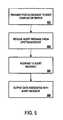
- FIG. 5is a flow diagram illustrating a method according to some embodiments. The method might be performed, for example, by the downstream device 120 of FIG. 1 or the endpoint device 320 of FIG. 3 .
- a posted requestis transmitted upstream to a root complex or switch.
- the posted requestmight comprise, for example, a memory write request.
- an alert messageis received from an upstream device.
- a PCI Express Vendor Defined Message Type-1 packetmight be received with a vendor ID and vendor defined data indicating that the packet is an alert packet.
- the downstream devicemight try to respond to the alert message at 506 .
- the downstream devicemight re-set itself or otherwise attempt to recover from a bad state.
- the downstream devicemight log and/or output data associated with the alert message. For example, the downstream device might output data associated with the last packet successfully processed by the root complex along with data from an uncorrectable error status register. Note that someone trying to debug an error might be interested in determining when the error occurred and/or other details about the error. Although a logic analyzer could be coupled to various interfaces (e.g., a system bus) to determine this type of information, such an approach can be difficult and time consuming (especially when the apparatus is associated with a mobile platform). According to some embodiments, the downstream device can directly output information associated with an error to facilitate a debugging process.
- various interfacese.g., a system bus
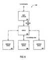
- FIG. 6is a block diagram of an apparatus 600 according to some embodiments.
- a switch 640is coupled to a root complex 610 and a number of different endpoint devices 620 via a plurality of PCI Express links.
- an endpoint device 620might send a posted request to the switch 640 , which in turn forwards the request to the root complex 610 .
- the switch 640may detect an error and send an alert message to the appropriate endpoint device 620 .
- the root complex 610will detect an error and send an alert message to the switch 640 (which in turn may forward the alert message to the appropriate endpoint device 620 ).
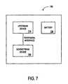
- FIG. 7is a block diagram of a system 700 according to some embodiments.
- the system 700might be associated with, for example, a PC, a mobile computer, a server, a wireless device, a game device, or a media device (e.g., a Digital Video Recorder (DVR) or set-top box).
- the system 700may include an upstream device 710 and a downstream device 720 in accordance with any of the embodiments described herein.
- the upstream device 710may be an interface device (e.g., a root complex or switch) adapted to detect an error associated with a request, and to transmit an alert message to the downstream device 720 via a peripheral interface.
- the downstream device 720might comprise, for example, an endpoint device (e.g., a peripheral) adapted to receive the alert message.
- the system 700further includes a battery 730 (e.g., to provide power to a processor and/or to provide power when the system 700 is turned off).
Landscapes
- Engineering & Computer Science (AREA)
- Theoretical Computer Science (AREA)
- Quality & Reliability (AREA)
- Physics & Mathematics (AREA)
- General Engineering & Computer Science (AREA)
- General Physics & Mathematics (AREA)
- Computer Networks & Wireless Communication (AREA)
- Signal Processing (AREA)
- Debugging And Monitoring (AREA)
Abstract
Description
Claims (18)
Priority Applications (1)
| Application Number | Priority Date | Filing Date | Title |
|---|---|---|---|
| US13/728,161US8656069B2 (en) | 2005-06-20 | 2012-12-27 | Peripheral interface alert message for downstream device |
Applications Claiming Priority (3)
| Application Number | Priority Date | Filing Date | Title |
|---|---|---|---|
| US11/156,838US7970958B2 (en) | 2005-06-20 | 2005-06-20 | Peripheral interface alert message for downstream device |
| US13/111,673US8346992B2 (en) | 2005-06-20 | 2011-05-19 | Peripheral interface alert message for downstream device |
| US13/728,161US8656069B2 (en) | 2005-06-20 | 2012-12-27 | Peripheral interface alert message for downstream device |
Related Parent Applications (1)
| Application Number | Title | Priority Date | Filing Date |
|---|---|---|---|
| US13/111,673ContinuationUS8346992B2 (en) | 2005-06-20 | 2011-05-19 | Peripheral interface alert message for downstream device |
Publications (2)
| Publication Number | Publication Date |
|---|---|
| US20130151887A1 US20130151887A1 (en) | 2013-06-13 |
| US8656069B2true US8656069B2 (en) | 2014-02-18 |
Family
ID=37574672
Family Applications (3)
| Application Number | Title | Priority Date | Filing Date |
|---|---|---|---|
| US11/156,838Active2026-11-12US7970958B2 (en) | 2005-06-20 | 2005-06-20 | Peripheral interface alert message for downstream device |
| US13/111,673Expired - LifetimeUS8346992B2 (en) | 2005-06-20 | 2011-05-19 | Peripheral interface alert message for downstream device |
| US13/728,161Expired - LifetimeUS8656069B2 (en) | 2005-06-20 | 2012-12-27 | Peripheral interface alert message for downstream device |
Family Applications Before (2)
| Application Number | Title | Priority Date | Filing Date |
|---|---|---|---|
| US11/156,838Active2026-11-12US7970958B2 (en) | 2005-06-20 | 2005-06-20 | Peripheral interface alert message for downstream device |
| US13/111,673Expired - LifetimeUS8346992B2 (en) | 2005-06-20 | 2011-05-19 | Peripheral interface alert message for downstream device |
Country Status (1)
| Country | Link |
|---|---|
| US (3) | US7970958B2 (en) |
Families Citing this family (16)
| Publication number | Priority date | Publication date | Assignee | Title |
|---|---|---|---|---|
| US7970958B2 (en) | 2005-06-20 | 2011-06-28 | Micron Technology, Inc. | Peripheral interface alert message for downstream device |
| US7730361B2 (en)* | 2007-03-30 | 2010-06-01 | Texas Instruments Incorporated | Aggregation of error messaging in multifunction PCI express devices |
| US8776080B2 (en)* | 2007-09-25 | 2014-07-08 | Intel Corporationa | Management component transport protocol interconnect filtering and routing |
| US7774638B1 (en)* | 2007-09-27 | 2010-08-10 | Unisys Corporation | Uncorrectable data error containment systems and methods |
| US8463881B1 (en) | 2007-10-01 | 2013-06-11 | Apple Inc. | Bridging mechanism for peer-to-peer communication |
| US20110090042A1 (en)* | 2009-10-21 | 2011-04-21 | Leviton Manufacturing Co., Inc. | Wireless demand response system |
| US8327536B2 (en) | 2010-06-30 | 2012-12-11 | Apple Inc. | Method of manufacturing high-speed connector inserts and cables |
| KR101758968B1 (en) | 2010-06-30 | 2017-07-17 | 애플 인크. | Circuitry for active cable |
| US9112310B2 (en) | 2010-06-30 | 2015-08-18 | Apple Inc. | Spark gap for high-speed cable connectors |
| US8291146B2 (en)* | 2010-07-15 | 2012-10-16 | Ati Technologies Ulc | System and method for accessing resources of a PCI express compliant device |
| US20120226774A1 (en) | 2011-02-23 | 2012-09-06 | Apple Inc. | Display snooping |
| US10764532B2 (en)* | 2012-10-30 | 2020-09-01 | Viavi Solutions Inc. | Method and system for locating ingress utilizing customer premises equipment |
| US9298529B2 (en) | 2014-05-29 | 2016-03-29 | Freescale Semiconductor, Inc. | Indicating internal transmitter errors in a controller area network (CAN) |
| US11017071B2 (en)* | 2018-08-02 | 2021-05-25 | Dell Products L.P. | Apparatus and method to protect an information handling system against other devices |
| CN113906400B (en)* | 2019-04-29 | 2024-09-24 | 迈凌有限公司 | System communication techniques via PCIe (high speed serial computer expansion bus) link |
| CN114357048A (en)* | 2022-01-05 | 2022-04-15 | 携程旅游网络技术(上海)有限公司 | Interface fusing method and system, electronic equipment and storage medium |
Citations (28)
| Publication number | Priority date | Publication date | Assignee | Title |
|---|---|---|---|---|
| US3749845A (en) | 1971-08-27 | 1973-07-31 | Bell Telephone Labor Inc | Digital data communication system |
| USRE31319E (en) | 1971-08-27 | 1983-07-19 | Bell Telephone Laboratories, Incorporated | Digital data communication system |
| US5163151A (en) | 1990-03-22 | 1992-11-10 | Square D Company | System for processing and prioritizing alarms from devices on data communications network |
| US5673252A (en) | 1990-02-15 | 1997-09-30 | Itron, Inc. | Communications protocol for remote data generating stations |
| US5961605A (en) | 1997-02-06 | 1999-10-05 | Gte Laboratories Incorporated | Method and apparatus for acknowledging TCP data packets |
| US6181704B1 (en) | 1997-08-29 | 2001-01-30 | Intel Corporation | Method and apparatus for input/output link retry, failure and recovery in a computer network |
| US20020142720A1 (en) | 2001-03-27 | 2002-10-03 | Russell Richard Francis | Method of sharing a printer |
| US6662319B1 (en) | 2000-08-31 | 2003-12-09 | Hewlett-Packard Development Company, L.P. | Special encoding of known bad data |
| US6674751B1 (en) | 1999-06-03 | 2004-01-06 | Fujitsu Network Communications, Inc. | Serialized bus communication and control architecture |
| US20040059978A1 (en) | 2002-06-25 | 2004-03-25 | Parvathanathan Subrahmanya | Reduced latency for recovery from communications errors |
| US20040073658A1 (en) | 2002-10-10 | 2004-04-15 | Cisco Technology, Inc. | System and method for distributed diagnostics in a communication system |
| US6744765B1 (en) | 2000-08-24 | 2004-06-01 | Sun Microsystems, Inc. | Mechanism for completing messages in memory |
| US6774765B1 (en) | 1998-06-18 | 2004-08-10 | Ncr Corporation | System and method of dispatching an individual in a transaction establishment |
| US20050034045A1 (en) | 2003-08-08 | 2005-02-10 | Lueck Andrew W. | System for optimizing PCI-Express communications |
| US20050120163A1 (en) | 2003-12-02 | 2005-06-02 | Super Talent Electronics Inc. | Serial Interface to Flash-Memory Chip Using PCI-Express-Like Packets and Packed Data for Partial-Page Writes |
| US20050207726A1 (en) | 2004-03-22 | 2005-09-22 | Jui-Ming Chen | Portable multimedia electronic device |
| US20060013155A1 (en) | 2004-07-15 | 2006-01-19 | Spaete Lawrence Jr | Method and system for identifying a defective cable modem in an S-CDMA environment |
| US20060230210A1 (en) | 2005-03-31 | 2006-10-12 | Intel Corporation | Method and apparatus for memory interface |
| US20060239095A1 (en) | 2005-03-30 | 2006-10-26 | Jun Shi | Memory device communication using system memory bus |
| US20060282603A1 (en) | 2005-05-25 | 2006-12-14 | Integrated Device Technology, Inc. | Expansion of cross-domain addressing for PCI-express packets passing through non-transparent bridge |
| US20060282639A1 (en) | 2005-06-09 | 2006-12-14 | Infortrend Technology Inc. | Storage virtualization subsystem architecture |
| US20060288098A1 (en) | 2005-06-20 | 2006-12-21 | Singh Ajai K | Peripheral interface alert message for downstream device |
| US20070028152A1 (en) | 2005-08-01 | 2007-02-01 | Mishra Kishore K | System and Method of Processing Received Line Traffic for PCI Express that Provides Line-Speed Processing, and Provides Substantial Gate-Count Savings |
| US7370243B1 (en) | 2004-06-30 | 2008-05-06 | Sun Microsystems, Inc. | Precise error handling in a fine grain multithreaded multicore processor |
| US20080155356A1 (en) | 2006-12-21 | 2008-06-26 | Sap Ag | Processor-based system analysis automation |
| US8286027B2 (en)* | 2010-05-25 | 2012-10-09 | Oracle International Corporation | Input/output device including a mechanism for accelerated error handling in multiple processor and multi-function systems |
| US20130031419A1 (en)* | 2011-07-28 | 2013-01-31 | International Business Machines Corporation | Collecting Debug Data in a Secure Chip Implementation |
| US20130055030A1 (en)* | 2011-08-25 | 2013-02-28 | Ultrasoc Technologies Ltd. | Data Processing Apparatus and Related Methods of Debugging Processing Circuitry |
- 2005
- 2005-06-20USUS11/156,838patent/US7970958B2/enactiveActive
- 2011
- 2011-05-19USUS13/111,673patent/US8346992B2/ennot_activeExpired - Lifetime
- 2012
- 2012-12-27USUS13/728,161patent/US8656069B2/ennot_activeExpired - Lifetime
Patent Citations (33)
| Publication number | Priority date | Publication date | Assignee | Title |
|---|---|---|---|---|
| USRE31319E (en) | 1971-08-27 | 1983-07-19 | Bell Telephone Laboratories, Incorporated | Digital data communication system |
| US3749845A (en) | 1971-08-27 | 1973-07-31 | Bell Telephone Labor Inc | Digital data communication system |
| US5673252A (en) | 1990-02-15 | 1997-09-30 | Itron, Inc. | Communications protocol for remote data generating stations |
| US5163151A (en) | 1990-03-22 | 1992-11-10 | Square D Company | System for processing and prioritizing alarms from devices on data communications network |
| US5961605A (en) | 1997-02-06 | 1999-10-05 | Gte Laboratories Incorporated | Method and apparatus for acknowledging TCP data packets |
| US6272550B1 (en) | 1997-02-06 | 2001-08-07 | Verizon Laboratories Inc. | Method and apparatus for acknowledging top data packets |
| US6181704B1 (en) | 1997-08-29 | 2001-01-30 | Intel Corporation | Method and apparatus for input/output link retry, failure and recovery in a computer network |
| US6774765B1 (en) | 1998-06-18 | 2004-08-10 | Ncr Corporation | System and method of dispatching an individual in a transaction establishment |
| US6674751B1 (en) | 1999-06-03 | 2004-01-06 | Fujitsu Network Communications, Inc. | Serialized bus communication and control architecture |
| US6744765B1 (en) | 2000-08-24 | 2004-06-01 | Sun Microsystems, Inc. | Mechanism for completing messages in memory |
| US7100096B2 (en) | 2000-08-31 | 2006-08-29 | Hewlett-Packard Development Company, L.P. | Special encoding of known bad data |
| US6662319B1 (en) | 2000-08-31 | 2003-12-09 | Hewlett-Packard Development Company, L.P. | Special encoding of known bad data |
| US20020142720A1 (en) | 2001-03-27 | 2002-10-03 | Russell Richard Francis | Method of sharing a printer |
| US20040059978A1 (en) | 2002-06-25 | 2004-03-25 | Parvathanathan Subrahmanya | Reduced latency for recovery from communications errors |
| US20040073658A1 (en) | 2002-10-10 | 2004-04-15 | Cisco Technology, Inc. | System and method for distributed diagnostics in a communication system |
| US20050034045A1 (en) | 2003-08-08 | 2005-02-10 | Lueck Andrew W. | System for optimizing PCI-Express communications |
| US20050120163A1 (en) | 2003-12-02 | 2005-06-02 | Super Talent Electronics Inc. | Serial Interface to Flash-Memory Chip Using PCI-Express-Like Packets and Packed Data for Partial-Page Writes |
| US20050207726A1 (en) | 2004-03-22 | 2005-09-22 | Jui-Ming Chen | Portable multimedia electronic device |
| US7370243B1 (en) | 2004-06-30 | 2008-05-06 | Sun Microsystems, Inc. | Precise error handling in a fine grain multithreaded multicore processor |
| US20060013155A1 (en) | 2004-07-15 | 2006-01-19 | Spaete Lawrence Jr | Method and system for identifying a defective cable modem in an S-CDMA environment |
| US20060239095A1 (en) | 2005-03-30 | 2006-10-26 | Jun Shi | Memory device communication using system memory bus |
| US20060230210A1 (en) | 2005-03-31 | 2006-10-12 | Intel Corporation | Method and apparatus for memory interface |
| US20060282603A1 (en) | 2005-05-25 | 2006-12-14 | Integrated Device Technology, Inc. | Expansion of cross-domain addressing for PCI-express packets passing through non-transparent bridge |
| US20060282639A1 (en) | 2005-06-09 | 2006-12-14 | Infortrend Technology Inc. | Storage virtualization subsystem architecture |
| US7970958B2 (en) | 2005-06-20 | 2011-06-28 | Micron Technology, Inc. | Peripheral interface alert message for downstream device |
| US20060288098A1 (en) | 2005-06-20 | 2006-12-21 | Singh Ajai K | Peripheral interface alert message for downstream device |
| US20110225469A1 (en) | 2005-06-20 | 2011-09-15 | Singh Ajai K | Peripheral interface alert message for downstream device |
| US20070028152A1 (en) | 2005-08-01 | 2007-02-01 | Mishra Kishore K | System and Method of Processing Received Line Traffic for PCI Express that Provides Line-Speed Processing, and Provides Substantial Gate-Count Savings |
| US20080155356A1 (en) | 2006-12-21 | 2008-06-26 | Sap Ag | Processor-based system analysis automation |
| US8286027B2 (en)* | 2010-05-25 | 2012-10-09 | Oracle International Corporation | Input/output device including a mechanism for accelerated error handling in multiple processor and multi-function systems |
| US20130031419A1 (en)* | 2011-07-28 | 2013-01-31 | International Business Machines Corporation | Collecting Debug Data in a Secure Chip Implementation |
| US20130031420A1 (en)* | 2011-07-28 | 2013-01-31 | International Business Machines Corporation | Collecting Debug Data in a Secure Chip Implementation |
| US20130055030A1 (en)* | 2011-08-25 | 2013-02-28 | Ultrasoc Technologies Ltd. | Data Processing Apparatus and Related Methods of Debugging Processing Circuitry |
Non-Patent Citations (25)
Also Published As
| Publication number | Publication date |
|---|---|
| US20110225469A1 (en) | 2011-09-15 |
| US7970958B2 (en) | 2011-06-28 |
| US8346992B2 (en) | 2013-01-01 |
| US20130151887A1 (en) | 2013-06-13 |
| US20060288098A1 (en) | 2006-12-21 |
Similar Documents
| Publication | Publication Date | Title |
|---|---|---|
| US8656069B2 (en) | Peripheral interface alert message for downstream device | |
| US6766479B2 (en) | Apparatus and methods for identifying bus protocol violations | |
| US7685476B2 (en) | Early notification of error via software interrupt and shared memory write | |
| CN100440157C (en) | System and method for logging recoverable errors | |
| US9665456B2 (en) | Apparatus and method for identifying a cause of an error occurring in a network connecting devices within an information processing apparatus | |
| CN101126995A (en) | Method and apparatus for processing serious hardware error | |
| US8726102B2 (en) | System and method for handling system failure | |
| US7178054B2 (en) | Frame validation | |
| US6604161B1 (en) | Translation of PCI level interrupts into packet based messages for edge event drive microprocessors | |
| WO2024016864A1 (en) | Processor, information acquisition method, single board and network device | |
| US8065566B2 (en) | Node device, control device, control method and control program | |
| CN100375960C (en) | Method and apparatus for regulating input/output fault | |
| US7272745B2 (en) | Data protection system | |
| US8880957B2 (en) | Facilitating processing in a communications environment using stop signaling | |
| CN101458650B (en) | Apparatus and method for detecting internal memory transfer abnormity in multi-core system | |
| WO2023028741A1 (en) | Advanced extensible interface bus and on-chip system | |
| US7478262B2 (en) | Method for allowing distributed high performance coherent memory with full error containment | |
| CN107451028A (en) | Error condition storage method and server | |
| US20040003160A1 (en) | Method and apparatus for provision, access and control of an event log for a plurality of internal modules of a chipset | |
| US7500154B2 (en) | Method and system for generating a console log | |
| CN116467132A (en) | Terminal equipment security chip debugging method and system | |
| CN118885321A (en) | AI server fault positioning method | |
| JPH05224964A (en) | Bus abnormality information system | |
| JP4439295B2 (en) | Data transfer control device | |
| US20060088163A1 (en) | Integrated circuit capable of pre-descrambling a portion of a frame |
Legal Events
| Date | Code | Title | Description |
|---|---|---|---|
| FEPP | Fee payment procedure | Free format text:PAYOR NUMBER ASSIGNED (ORIGINAL EVENT CODE: ASPN); ENTITY STATUS OF PATENT OWNER: LARGE ENTITY | |
| STCF | Information on status: patent grant | Free format text:PATENTED CASE | |
| CC | Certificate of correction | ||
| AS | Assignment | Owner name:U.S. BANK NATIONAL ASSOCIATION, AS COLLATERAL AGENT, CALIFORNIA Free format text:SECURITY INTEREST;ASSIGNOR:MICRON TECHNOLOGY, INC.;REEL/FRAME:038669/0001 Effective date:20160426 Owner name:U.S. BANK NATIONAL ASSOCIATION, AS COLLATERAL AGEN Free format text:SECURITY INTEREST;ASSIGNOR:MICRON TECHNOLOGY, INC.;REEL/FRAME:038669/0001 Effective date:20160426 | |
| AS | Assignment | Owner name:MORGAN STANLEY SENIOR FUNDING, INC., AS COLLATERAL AGENT, MARYLAND Free format text:PATENT SECURITY AGREEMENT;ASSIGNOR:MICRON TECHNOLOGY, INC.;REEL/FRAME:038954/0001 Effective date:20160426 Owner name:MORGAN STANLEY SENIOR FUNDING, INC., AS COLLATERAL Free format text:PATENT SECURITY AGREEMENT;ASSIGNOR:MICRON TECHNOLOGY, INC.;REEL/FRAME:038954/0001 Effective date:20160426 | |
| AS | Assignment | Owner name:U.S. BANK NATIONAL ASSOCIATION, AS COLLATERAL AGENT, CALIFORNIA Free format text:CORRECTIVE ASSIGNMENT TO CORRECT THE REPLACE ERRONEOUSLY FILED PATENT #7358718 WITH THE CORRECT PATENT #7358178 PREVIOUSLY RECORDED ON REEL 038669 FRAME 0001. ASSIGNOR(S) HEREBY CONFIRMS THE SECURITY INTEREST;ASSIGNOR:MICRON TECHNOLOGY, INC.;REEL/FRAME:043079/0001 Effective date:20160426 Owner name:U.S. BANK NATIONAL ASSOCIATION, AS COLLATERAL AGEN Free format text:CORRECTIVE ASSIGNMENT TO CORRECT THE REPLACE ERRONEOUSLY FILED PATENT #7358718 WITH THE CORRECT PATENT #7358178 PREVIOUSLY RECORDED ON REEL 038669 FRAME 0001. ASSIGNOR(S) HEREBY CONFIRMS THE SECURITY INTEREST;ASSIGNOR:MICRON TECHNOLOGY, INC.;REEL/FRAME:043079/0001 Effective date:20160426 | |
| FPAY | Fee payment | Year of fee payment:4 | |
| AS | Assignment | Owner name:JPMORGAN CHASE BANK, N.A., AS COLLATERAL AGENT, ILLINOIS Free format text:SECURITY INTEREST;ASSIGNORS:MICRON TECHNOLOGY, INC.;MICRON SEMICONDUCTOR PRODUCTS, INC.;REEL/FRAME:047540/0001 Effective date:20180703 Owner name:JPMORGAN CHASE BANK, N.A., AS COLLATERAL AGENT, IL Free format text:SECURITY INTEREST;ASSIGNORS:MICRON TECHNOLOGY, INC.;MICRON SEMICONDUCTOR PRODUCTS, INC.;REEL/FRAME:047540/0001 Effective date:20180703 | |
| AS | Assignment | Owner name:MICRON TECHNOLOGY, INC., IDAHO Free format text:RELEASE BY SECURED PARTY;ASSIGNOR:U.S. BANK NATIONAL ASSOCIATION, AS COLLATERAL AGENT;REEL/FRAME:047243/0001 Effective date:20180629 | |
| AS | Assignment | Owner name:MICRON TECHNOLOGY, INC., IDAHO Free format text:RELEASE BY SECURED PARTY;ASSIGNOR:MORGAN STANLEY SENIOR FUNDING, INC., AS COLLATERAL AGENT;REEL/FRAME:050937/0001 Effective date:20190731 | |
| AS | Assignment | Owner name:MICRON SEMICONDUCTOR PRODUCTS, INC., IDAHO Free format text:RELEASE BY SECURED PARTY;ASSIGNOR:JPMORGAN CHASE BANK, N.A., AS COLLATERAL AGENT;REEL/FRAME:051028/0001 Effective date:20190731 Owner name:MICRON TECHNOLOGY, INC., IDAHO Free format text:RELEASE BY SECURED PARTY;ASSIGNOR:JPMORGAN CHASE BANK, N.A., AS COLLATERAL AGENT;REEL/FRAME:051028/0001 Effective date:20190731 | |
| MAFP | Maintenance fee payment | Free format text:PAYMENT OF MAINTENANCE FEE, 8TH YEAR, LARGE ENTITY (ORIGINAL EVENT CODE: M1552); ENTITY STATUS OF PATENT OWNER: LARGE ENTITY Year of fee payment:8 | |
| MAFP | Maintenance fee payment | Free format text:PAYMENT OF MAINTENANCE FEE, 12TH YEAR, LARGE ENTITY (ORIGINAL EVENT CODE: M1553); ENTITY STATUS OF PATENT OWNER: LARGE ENTITY Year of fee payment:12 |