US8653583B2 - Sensing FET integrated with a high-voltage transistor - Google Patents
Sensing FET integrated with a high-voltage transistorDownload PDFInfo
- Publication number
- US8653583B2 US8653583B2US11/707,586US70758607AUS8653583B2US 8653583 B2US8653583 B2US 8653583B2US 70758607 AUS70758607 AUS 70758607AUS 8653583 B2US8653583 B2US 8653583B2
- Authority
- US
- United States
- Prior art keywords
- pillar
- region
- substrate
- transistor
- main vertical
- Prior art date
- Legal status (The legal status is an assumption and is not a legal conclusion. Google has not performed a legal analysis and makes no representation as to the accuracy of the status listed.)
- Active, expires
Links
Images


Classifications
- H—ELECTRICITY
- H10—SEMICONDUCTOR DEVICES; ELECTRIC SOLID-STATE DEVICES NOT OTHERWISE PROVIDED FOR
- H10D—INORGANIC ELECTRIC SEMICONDUCTOR DEVICES
- H10D30/00—Field-effect transistors [FET]
- H10D30/60—Insulated-gate field-effect transistors [IGFET]
- H10D30/64—Double-diffused metal-oxide semiconductor [DMOS] FETs
- H10D30/66—Vertical DMOS [VDMOS] FETs
- H10D30/669—Vertical DMOS [VDMOS] FETs having voltage-sensing or current-sensing structures, e.g. emulator sections or overcurrent sensing cells
- H—ELECTRICITY
- H10—SEMICONDUCTOR DEVICES; ELECTRIC SOLID-STATE DEVICES NOT OTHERWISE PROVIDED FOR
- H10D—INORGANIC ELECTRIC SEMICONDUCTOR DEVICES
- H10D30/00—Field-effect transistors [FET]
- H10D30/60—Insulated-gate field-effect transistors [IGFET]
- H10D30/64—Double-diffused metal-oxide semiconductor [DMOS] FETs
- H10D30/66—Vertical DMOS [VDMOS] FETs
- H10D30/668—Vertical DMOS [VDMOS] FETs having trench gate electrodes, e.g. UMOS transistors
- H—ELECTRICITY
- H10—SEMICONDUCTOR DEVICES; ELECTRIC SOLID-STATE DEVICES NOT OTHERWISE PROVIDED FOR
- H10D—INORGANIC ELECTRIC SEMICONDUCTOR DEVICES
- H10D62/00—Semiconductor bodies, or regions thereof, of devices having potential barriers
- H10D62/10—Shapes, relative sizes or dispositions of the regions of the semiconductor bodies; Shapes of the semiconductor bodies
- H10D62/124—Shapes, relative sizes or dispositions of the regions of semiconductor bodies or of junctions between the regions
- H10D62/126—Top-view geometrical layouts of the regions or the junctions
- H10D62/127—Top-view geometrical layouts of the regions or the junctions of cellular field-effect devices, e.g. multicellular DMOS transistors or IGBTs
- H—ELECTRICITY
- H10—SEMICONDUCTOR DEVICES; ELECTRIC SOLID-STATE DEVICES NOT OTHERWISE PROVIDED FOR
- H10D—INORGANIC ELECTRIC SEMICONDUCTOR DEVICES
- H10D64/00—Electrodes of devices having potential barriers
- H10D64/111—Field plates
- H10D64/117—Recessed field plates, e.g. trench field plates or buried field plates
Definitions
- the present disclosurerelates to semiconductor devices, device structures, and processes for fabricating high-voltage or power transistor devices.
- Sensefetsare typically constructed as a small part or transistor section of a larger, main current carrying semiconductor device.
- the sensefetmay comprise a small section of the channel region of the main device.
- the sensefetmay sample a small portion of the channel current of the larger device, thereby providing an indication of the current flowing through the main transistor device.
- the sensefet and main devicetypically share a common drain and gate, but each has a separate source electrode.
- High-voltage, field-effect transistorsare also well known in the semiconductor arts.
- Many HVFETsi.e., power transistors
- a device structurethat includes an extended drain or drift region that supports or blocks the applied high-voltage (e.g., several hundred volts) when the device is in the “off” state.
- a mesa or pillar of semiconductor materialforms the extended drain or drift region for current flow in the on-state.
- a trench gate structureis formed near the top of the substrate, adjacent the sidewall regions of the mesa where a body region is disposed above the extended drain region.
- a conductive channelto be formed along the vertical sidewall portion of the body region such that current may flow vertically through the semiconductor material, i.e., from a top surface of the substrate where the source region is disposed, down to the bottom of the substrate where the drain region is located.
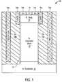
- FIG. 1illustrates an example cross-sectional side view of a vertical HVFET structure.
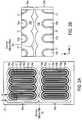
- FIG. 2Aillustrates an example layout of the vertical HVFET structure shown in FIG. 1 .
- FIG. 2Bis an expanded view of one portion of the example layout shown in FIG. 2A .
- FIG. 3Aillustrates another example layout of the vertical HVFET structure shown in FIG. 1 .
- FIG. 3Bis an expanded view of one portion of the example layout shown in FIG. 3A .
- FIG. 4Aillustrates yet another example layout of the vertical HVFET structure shown in FIG. 1 .
- FIG. 4Bis an expanded view of one portion of the example layout shown in FIG. 4A .
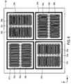
- FIG. 5illustrates an example layout of a wafer with die-to-die checkerboarding of HVFETs.
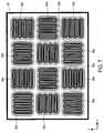
- FIG. 6illustrates an example layout of a wafer with die-to-die checkerboarding of segmented HVFETs.
- FIG. 7illustrates an example layout of a rectangular die with checkerboarded blocks of HVFET segments.
- FIG. 8Ais a top view of a portion of an example layout of a sensefet incorporated in the vertical HVFET structure shown in FIG. 1 .
- FIG. 8Bis a cross-sectional side view taken through cut lines A-A′ of the example layout shown in FIG. 8A .
- FIG. 9is an example circuit schematic diagram of the integrated device structure shown in FIGS. 8A & 8B .
- FIG. 10Ais a top view of a portion of another example layout of a sensefet incorporated in the vertical HVFET structure shown in FIG. 1 .
- FIG. 10Bis a cross-sectional side view taken through cut lines B-B′ of the sensefet and HVFET shown in FIG. 10A .
- FIG. 11is an example circuit schematic diagram of the integrated device structure shown in FIGS. 10A & 10B .
- FIG. 12Ais a top view of a portion of yet another example layout of a sensefet incorporated in the vertical HVFET structure shown in FIG. 1 .
- FIG. 12Bis a cross-sectional side view taken through cut lines C-C′ of the device structure shown in FIG. 12A .
- FIG. 12Ca cross-sectional side view taken through cut lines D-D′ of the device structure shown in FIG. 12A .
- FIG. 13is an example circuit schematic diagram of the integrated device structure shown in FIGS. 12A-12C .
- FIG. 1illustrates an example cross-sectional side view of a vertical HVFET 10 having a structure that includes an extended drain region 12 of N-type silicon formed on an N+ doped silicon substrate 11 .
- Substrate 11is heavily doped to minimize its resistance to current flowing through to the drain electrode, which is located on the bottom of the substrate in the completed device.
- extended drain region 12is part of an epitaxial layer that extends from substrate 11 to a top surface of the silicon wafer.
- a P-type body region 13 and N+ doped source regions 14 a & 14 b laterally separated by a P-type region 16are formed near a top surface of the epitaxial layer.
- P-type body region 13is disposed above and vertically separates extended drain region 12 from N+ source regions 14 a & 14 b and P-type region 16 .
- the doping concentration of the portion of epitaxial layer which comprises extended drain region 12is linearly graded to produce an extended drain region that exhibits a substantially uniform electric-field distribution. Linear grading may stop at some point below the top surface of the epitaxial layer 12 .
- Extended drain region 12 , body region 13 , source regions 14 a & 14 b and P-type region 16collectively comprise a mesa or pillar 17 (both terms are used synonymously in the present application) of silicon material in the example vertical transistor of FIG. 1 .
- Vertical trenches formed on opposite sides of pillar 17are filled with a layer of dielectric material (e.g., oxide) that makes up dielectric region 15 .
- the height and width of pillar 17 , as well as the spacing between adjacent vertical trenchesmay be determined by the breakdown voltage requirements of the device.
- mesa 17has a vertical height (thickness) in a range of about 30 ⁇ m to 120 ⁇ m thick.
- a HVFET formed on a die approximately 1 mm ⁇ 1 mm in sizemay have a pillar 17 with a vertical thickness of about 60 ⁇ m.
- a transistor structure formed on a die of about 2 mm-4 mm on each sidemay have a pillar structure of approximately 30 ⁇ m thick.
- the lateral width of pillar 17is as narrow as can be reliably manufactured (e.g., about 0.4 ⁇ m to 0.8 ⁇ m wide) in order to achieve a very high breakdown voltage (e.g., 600-800V).
- N+ source regions and P-type regionsmay be alternately formed at the top of pillar 17 across the lateral length of pillar 17 .
- a given cross-sectional view such as that shown in FIG. 1would have either an N+ source region 14 , or a P-type region 16 , that extends across the full lateral width of pillar 17 , depending upon where the cross-section is taken.
- each N+ source region 14is adjoined on both sides (along the lateral length of the pillar) by P-type regions 16 .
- each P-type region 16is adjoined on both sides (along the lateral length of the pillar) by N+ source regions 14 .
- FIGS. 12A & 12Bdiscussed below.
- Dielectric regions 15 a & 15 bmay comprise silicon dioxide, silicon nitride, or other suitable dielectric materials. Dielectric regions 15 may be formed using a variety of well-known methods, including thermal growth and chemical vapor deposition. Disposed within each of the dielectric layers 15 , and fully insulated from substrate 11 and pillar 17 , is a field plate 19 .
- the conductive material used to from field plates 19may comprise a heavily doped polysilicon, a metal (or metal alloys), a silicide, or other suitable materials.
- field plates 19 a & 19 bnormally function as capacitive plates that may be used to deplete the extended drain region of charge when the HVFET is in the off state (i.e., when the drain is raised to a high voltage potential).
- the lateral thickness of oxide region 15 that separates each field plate 19 from the sidewall of pillar 17is approximately 4 ⁇ m.
- the trench gate structure of vertical HVFET transistor 80comprises gate members 18 a & 18 b , each respectively disposed in oxide regions 15 a & 15 b on opposite sides of pillar 17 between field plates 19 a & 19 b and body region 13 .
- a high-quality, thin (e.g., ⁇ 500 ⁇ ) gate oxide layerseparates gate members 18 from the sidewalls of pillar 17 adjacent body region 13 .
- Gate members 18may comprise polysilicon, or some other suitable material.
- each gate member 18has a lateral width of approximately 1.5 ⁇ m and a depth of about 3.5 ⁇ m.
- N+ source regions 14 and P-type body region 13 near the top of pillar 17may each be formed using ordinary deposition, diffusion, and/or implantation processing techniques.
- HVFET 10may be completed by forming source, drain, gate, and field plate electrodes that electrically connect to the respective regions/materials of the device using conventional fabrication methods (not shown in the figures for clarity reasons).
- FIG. 2Aillustrates an example layout of the vertical HVFET structure shown in FIG. 1 .
- the top view of FIG. 2Ashows a single, discrete HVFET comprising an upper transistor section 30 a and a lower transistor section 30 b on a semiconductor die 21 .
- the two sectionsare separated by a dummy silicon pillar 32 .
- Each section 30comprises a plurality of “racetrack” shaped transistor structures or segments, each transistor segment comprises an elongated ring or oval that includes a silicon pillar 17 surrounded on opposite sides by dielectric regions 15 a & 15 b . Pillar 17 , itself, extends laterally in the x and y directions to form a continuous, elongated, racetrack-shaped ring or oval.
- Field plate 19 acomprises a single elongated member that terminates on either end in a rounded fingertip area.
- Field plate 19 bcomprises an enlarged ring or oval that encircles pillar 17 .
- Field plates 19 b of adjacent racetrack structuresare shown merged such that they share a common member on a side.
- the cross-sectional view of FIG. 1may be taken through cut lines A-A′ of the example layout of FIG. 2A .
- each of the racetrack transistor segmentshas a width (i.e., pitch) in the y-direction of approximately 13 ⁇ m, a length in the x-direction in a range of about 400 ⁇ m to 1000 ⁇ m, with a pillar height of about 60 ⁇ m.
- the length to width ratio of the individual racetrack transistor segments comprising sections 30 a & 30 bis in a range of about 30 up to 80.
- the length of each racetrack shaped segmentis at least 20 times greater than its pitch or width.
- patterned metal layersare used to interconnect each of the silicon pillars 17 of the individual transistor segments. That is, in a practical embodiment, all of the source regions, gate members, and field plates are respectively wired together to corresponding electrodes on the die.
- the transistor segments in each section 30are arranged in a side-by-side relationship in the y-direction substantially across a width of die 21 .
- the additive length of the transistor segments of sections 30 a & 30 bextend substantially over the length of die 21 .
- the width of dielectric regions 15 separating the silicon pillars, as well as the width of the field plates,is substantially uniform across semiconductor die 21 .
- Laying out the transistor segments with uniform widths and separation distancesprevents the formation of voids or holes following the processing steps used to conformably deposit the layers that comprise dielectric regions 15 and field plates 19 .
- FIG. 2Bis an expanded view of one portion of the example layout shown in FIG. 2A .
- Dummy silicon pillar 32is shown separating the rounded end areas of dielectric regions 15 b of respective transistor segment sections 30 a & 30 b .
- the deep vertical trenches that are etched in the semiconductor substrate to define pillars 17also define dummy silicon pillar 32 .
- dummy silicon pillar 32is made to have a width in the x-direction (i.e., that separates the transistor segment sections) that is as small as can be reliably manufactured.
- segmenting the single die HVFET into sections separated by dummy silicon pillar 32is to introduce lengthwise (x-direction) stress-relief in the elongated racetrack shaped transistor segments. Segmenting or breaking the transistor device structures into two or more sections relieves mechanical stress across the length of the die. This stress is induced by the oxide regions flanking the pillars and normally concentrates at the rounded ends of each racetrack segment. Relieving mechanical stress by segmenting the transistor device structures into two or more sections thus prevents undesirable warping of the silicon pillars and damage (e.g., dislocations) to the silicon caused by stress.
- damagee.g., dislocations
- a dummy pillar of siliconinstead of a dummy pillar of silicon to separate pairs of racetrack transistor segments, each pair being located in a different section, a dummy pillar comprising a different material may be utilized.
- the material used for the dummy pillarshould have a thermal coefficient of expansion close to that of silicon, or sufficiently different from that of the dielectric region so as to relieve the lengthwise stress induced by the dielectric regions flanking the silicon pillars.
- FIG. 3Aillustrates another example layout of the vertical HVFET structure shown in FIG. 1 .
- FIG. 3Bis an expanded view of one portion of the example layout shown in FIG. 3A , just showing pillars 17 , oxide region 15 b , and an optional dummy silicon pillar 33 .
- FIGS. 3A & 3Bshow a single, discrete HVFET comprising an upper transistor section 30 a and a lower transistor section 30 b on a semiconductor die 21 . But in the example of FIGS.
- a single dummy pillaris centrally located between the four rounded ends of adjacent pairs of transistor segments over the two sections.
- Nis an integer greater than 1
- racetrack segments or structures in a section 30 of the transistor comprising die 21there are a total of N ⁇ 1 dummy pillars 33 .
- FIG. 4Aillustrates yet another example layout of the vertical HVFET structure shown in FIG. 1 .
- FIG. 4Bis an expanded view of one portion of the example layout shown in FIG. 4A . Pillars 17 and oxide region 15 b are just shown for clarity reasons in the expanded view of FIG. 4B .
- the transistor segments comprising the HVFET of semiconductor die 21are alternately shifted by half of the length of each racetrack segment, resulting in racetrack transistor segments that are alternately associated with upper transistor section 40 a and lower transistor section 40 b .
- each of the transistor segments of a row of section 40 ais separated by a pair of the transistor segments of section 40 b , the pair being arranged in an end-to-end relationship in the x-direction.
- alternate shifting of the segmentsmay be any fraction of the segment length. In other words, shifting of the segments is not limited to 50% or half the length. Various embodiments may comprise segments alternately shifted by any percentage or fraction ranging from greater than 0% to less than 100% of the length of the transistor segments.
- the dielectric regions 15 b of alternating ones of the transistor segments in respective sections 40 a & 40 bare merged.
- the rounded ends of the transistor segments associated with different adjacent sectionsoverlap or are merged such that field plates 19 b of the adjacent sections are merged at the ends (in the x-direction).
- the extended straight side portions of field plates 19 b of alternating transistor segments of different sectionsare merged along a substantial length of each segment. It is appreciated that regions 15 b and 19 b may be merged with or without a dummy pillar (or isolated dummy silicon pillars) between the respective sections.
- FIG. 5illustrates an example layout of a wafer 50 with die-to-die checkerboarding of HVFETs 10 a - 10 d on semiconductor die 21 a - 21 d , respectively.
- HVFETs 10comprises a plurality of racetrack-shaped transistor segments such as that shown in FIG. 1 , arranged side-by-side along their width into a substantially square block.
- HVFETs 10 a - 10 deach comprises transistor segments having a length that extends substantially across the length of the respective die 21 a - 21 d .
- the width of each segmentis about 13 ⁇ m, with the length ranging from about 500 ⁇ m to 2000 ⁇ m. Other embodiments may have lengths greater than 2000 ⁇ m.
- the block or stacked arrangement of segmentsalso extends substantially across the width of each die. (Note that the bordered square of each die 21 represents the edge of the scribe area between adjacent semiconductor die.) Although FIG. 5 shows two rows and two columns of HVFETs 10 it is appreciated that the die-to-die checkerboarding arrangement shown may be repeated across the entire wafer substrate.
- adjacent die in a row or a columnare oriented such that the length of the transistor segments in one die extends in one direction, with the length of the transistor segments in an adjacent die extending in a second orthogonal direction.
- HVFET 10 ais shown with the length of its transistor segments oriented in the x-direction, whereas adjacent HVFETs 10 b & 10 c
- By orthogonally alternating the orientation of the transistor segments in each individual die 21 across wafer 50i.e., checkerboarding
- mechanical stress generated by the long dielectric regionsis distributed in two orthogonal directions, thus reducing warping of wafer 50 .
- FIG. 6illustrates another example layout of a wafer with die-to-die checkerboarding of segmented HVFETs.
- the example of FIG. 6utilizes the same approach as in FIG. 5 of alternating the orientation of the transistor structures die-to-die; however, in the embodiment of FIG. 6 , the HVFET structures are segmented into multiple (e.g., two) sections. For instance, each HVFET that extends substantially across the length and width of a semiconductor die 21 is segmented into two sections 30 a & 30 b separated by a dummy pillar 32 .
- Each of the semiconductor die 21 shown in FIG. 6has a layout that is the same as that shown in FIG. 2A for a substantially square die. Similar to the example shown in FIG. 5 , adjacent die have transistor segments that are orthogonally alternating across wafer 50 . That is, the transistor segments in sections 30 a & 30 b of die 21 a and 21 d have a length oriented in the x-direction, whereas the transistor segments in sections 30 a & 30 b of die 21 b and 21 c have a length oriented in the y-direction.
- the HVFET of each die 21may be formed with multiple transistor sections, e.g., greater than 2, each separated by one or more dummy pillars.
- any of the single die layouts with multiple transistor sections shown in the examples of FIGS. 2A-4Bmay be utilized in each of the die 21 shown in FIG. 6 , with the orientation of the segments alternating die-to-die across wafer 50 .
- FIG. 7illustrates an example rectangular layout of a die 25 with checkerboarded blocks of racetrack-shaped HVFET segments stacked in a side-by-side arrangement of substantially square blocks or sections 36 .
- Adjacent sections in a row or a columnare oriented such that the length of the transistor segments in one section extends in one direction, with the length of the transistor segments in the other adjacent section extending in a second orthogonal direction.
- each of the rows and columns of die 25include transistor sections 36 a oriented with the elongated transistor segments aligned in the x-direction and alternate transistor sections 36 b oriented with the elongated transistor segments aligned in the y-direction.
- the spaces between sections 36 a and 36 bcomprise dummy silicon pillars; that is, the silicon that forms the dummy pillars is not an active transistor region.
- die 25comprises three rows and four columns of transistor sections 36 .
- the checkerboarded layout approach shown in the example of FIG. 7may be used to produce a single, discrete HVFET on a die of virtually any (within practical limits) rectilinear-shape.
- FIG. 8Ais a top view of a portion of an example layout of a sensefet incorporated in the vertical HVFET structure shown in FIG. 1 .
- the sensefetis integrated into the same silicon pillar 17 as the main vertical power transistor device.
- FIG. 8Bis a cross-sectional side view taken through cut lines A-A′ of the example layout shown in FIG. 8A .
- FIG. 9is an example circuit schematic diagram of the integrated device structure shown in FIGS. 8A & 8B . Viewed collectively, the top of pillar 17 is seen comprising N+ source regions 14 and P+ regions 16 that alternate along the lateral length of the pillar in a given racetrack shaped transistor segment. For example, from left-to-right, FIGS.
- FIG. 8A & 8Billustrate regions 14 a , 16 a , 14 b , and 16 b that comprise the top portion of the vertical HVFET device 58 (see FIG. 9 ).
- P-body region 13extends to the top surface of pillar 17 to the immediate right of region 16 b , thereby separating region 16 b from N+ region 24 , which is associated with the sensefet device 59 .
- region 24comprises a small portion of the overall transistor segment (pillar) layout, such that sensefet 59 senses a small portion of the current flowing through the main vertical transistor device 58 .
- pillar 17is flanked on opposite lateral sides by gate members 18 a & 18 b , which are separated from the top portion of pillar 17 by gate oxide layers 20 a & 20 b , respectively.
- Source electrode 61electrically contacts each of regions 14 & 16 , while sense electrode 62 only contacts N+ region 24 of sensefet 59 .
- Source electrode 61may also electrically connect with the inner and outer field plate members 19 a & 19 b in certain embodiments.
- FIG. 9illustrates that vertical HVFET device 58 and sensefet 59 share a common gate 18 and a common drain node 63 .
- Extended drain region 12 and N+ substrate 11are shown as series connected resistors 64 and 65 , respectively, coupled between node 63 and drain electrode 71 , that latter being formed on the bottom surface of substrate 11 .
- electrode 62 of sensefet 59may be used to sample a small portion of the current flowing through the much larger vertical transistor device 58 , thereby providing an indication of the current flowing through main transistor 58 .
- FIG. 10Ais a top view of a portion of another example layout of a sensefet incorporated in the vertical HVFET structure shown in FIG. 1 .
- FIG. 10Bis a cross-sectional side view taken through cut lines B-B′ of the sensefet and HVFET shown in FIG. 10A .
- FIG. 11is an example circuit schematic diagram of the integrated device structure shown in FIGS. 10A & 10B . Note that the embodiment shown in FIGS. 10A , 10 B and 11 , sensefet 69 comprises P+ regions 25 and N+ regions 24 that alternate along the lateral length (i.e., around the racetrack shape) of pillar 17 .
- Each of regions 24 & 25are disposed in a P-body region 13 b that is separated from P-body region 13 a associated with main vertical transistor 68 by an area of extended drain region 12 that extends to the surface of pillar 17 .
- Each of P-body regions 13 a & 13 bextend to the surface of the pillar on both lateral sides of the alternating sequence of N+/P+ regions of respective transistors 68 & 69 .
- vertical HVFET device 68 and sensefet 69are shown sharing a common gate 18 and a common drain node 63 .
- the common extended drain region 64 and N+ substrate 65are shown as series connected resistors 64 and 65 , respectively, coupled between node 63 and drain electrode 71 .
- Source electrode 81electrically contacts each of regions 14 & 16 of main vertical transistor 68 , while sense electrode 82 only contacts regions 24 and 25 of sensefet 69 .
- Source electrode 81may also electrically connect with the inner and outer field plate members 19 a & 19 b in the metallization layout.
- FIG. 12Ais a top view of a portion of yet another example layout of a sensefet incorporated in the vertical HVFET structure shown in FIG. 1 .
- FIGS. 12B & 12 Care cross-sectional side views taken through cut lines C-C′ and D-D′, respectively, of the device structure shown in FIG. 12A . Note that in this embodiment, the sensefet and main vertical HVFET devices are formed on separate pillars that are isolated from each other.
- FIG. 12Bis a cross-section of main vertical transistor device 78 (associated with pillar 17 )
- FIG. 12Cis a cross-section of sensefet 79 (associated with pillar 17 ′).
- pillar 17 ′may comprise a single racetrack-shaped transistor segment dedicated to sensefet 79 disposed adjacent to a plurality of other similarly shaped transistor segments dedicated to main vertical transistor device 78 . It is appreciated that the main vertical HVFET device comprises a majority of the transistor segments on a die, with the sensefet comprising a minority (e.g., a single one) of the transistor segments.
- main vertical transistor device 78comprises alternating N+ regions 14 and P+ regions 16 disposed at the top of pillar 17 .
- Source electrode 91electrically contacts each of regions 14 & 16 .
- P-body region 13 aseparates regions 14 & 16 from underlying extended drain region 12 a .
- FIG. 12Cshows sensefet 79 comprising alternating N+ regions 24 and P+ regions 25 disposed at the top of pillar 17 ′.
- Sense electrode 92electrically contacts each of regions 24 & 25 .
- P-body region 13 bseparates regions 24 & 25 from underlying extended drain region 12 b.
- a resistor 65 representing the resistance of N+ substrate 11is shown between a common node 95 and drain electrode 71 .
- the resistance of extended drain region 12 bis shown as resistor 64 b connected between the drain of sensefet 79 and node 95 .
- the resistance of extended drain region 12 ais shown as resistor 64 a connected between the drain of main vertical transistor 78 and common node 95 .
- the equivalent circuit diagram of FIG. 13reflects the fact that even though sensefet 79 and main transistor 78 are formed on separate pillars, each pillar on the semiconductor die shares a common N+ substrate region.
Landscapes
- Metal-Oxide And Bipolar Metal-Oxide Semiconductor Integrated Circuits (AREA)
- Insulated Gate Type Field-Effect Transistor (AREA)
- Junction Field-Effect Transistors (AREA)
- Electrodes Of Semiconductors (AREA)
Abstract
Description
The present disclosure relates to semiconductor devices, device structures, and processes for fabricating high-voltage or power transistor devices.
Current sensing field-effect transistors, commonly referred to as sensefets, have been used widely used for many years in applications where accurate current sensing can provide information for both control and over-current protection. Sensefets are typically constructed as a small part or transistor section of a larger, main current carrying semiconductor device. For example, in a conventional insulated-gate field-effect transistor (MOSFET) device, the sensefet may comprise a small section of the channel region of the main device. In operation, the sensefet may sample a small portion of the channel current of the larger device, thereby providing an indication of the current flowing through the main transistor device. The sensefet and main device typically share a common drain and gate, but each has a separate source electrode.
High-voltage, field-effect transistors (HVFETs) are also well known in the semiconductor arts. Many HVFETs (i.e., power transistors) employ a device structure that includes an extended drain or drift region that supports or blocks the applied high-voltage (e.g., several hundred volts) when the device is in the “off” state. In a prior art vertical HVFET structure, a mesa or pillar of semiconductor material forms the extended drain or drift region for current flow in the on-state. A trench gate structure is formed near the top of the substrate, adjacent the sidewall regions of the mesa where a body region is disposed above the extended drain region. Application of an appropriate voltage potential to the gate causes a conductive channel to be formed along the vertical sidewall portion of the body region such that current may flow vertically through the semiconductor material, i.e., from a top surface of the substrate where the source region is disposed, down to the bottom of the substrate where the drain region is located.
One problem that exists is that prior art sensefets designed for use with conventional MOSFETs are generally inapplicable for use with vertical power transistor structures due to the deep trench that forms the pillar isolating both the channel and drift regions.
The present disclosure will be understood more fully from the detailed description that follows and from the accompanying drawings, which however, should not be taken to limit the invention to the specific embodiments shown, but are for explanation and understanding only.
In the following description specific details are set forth, such as material types, dimensions, structural features, processing steps, etc., in order to provide a thorough understanding of the present invention. However, persons having ordinary skill in the relevant arts will appreciate that these specific details may not be needed to practice the present invention. It should also be understood that the elements in the figures are representational, and are not drawn to scale in the interest of clarity.
In one embodiment, the doping concentration of the portion of epitaxial layer which comprises extendeddrain region 12 is linearly graded to produce an extended drain region that exhibits a substantially uniform electric-field distribution. Linear grading may stop at some point below the top surface of theepitaxial layer 12.
In another embodiment, instead of arranging P-type region 16 betweenN+ source regions 14a&14bacross the lateral width of pillar17 (as shown inFIG. 1 ), N+ source regions and P-type regions may be alternately formed at the top ofpillar 17 across the lateral length ofpillar 17. In other words, a given cross-sectional view such as that shown inFIG. 1 would have either an N+ source region14, or a P-type region 16, that extends across the full lateral width ofpillar 17, depending upon where the cross-section is taken. In such an embodiment, each N+ source region14 is adjoined on both sides (along the lateral length of the pillar) by P-type regions 16. Similarly, each P-type region 16 is adjoined on both sides (along the lateral length of the pillar) by N+ source regions14. (An example of such an embodiment is shown inFIGS. 12A & 12B , discussed below).
The trench gate structure of vertical HVFET transistor80 comprisesgate members 18a&18b, each respectively disposed inoxide regions 15a&15bon opposite sides ofpillar 17 betweenfield plates 19a&19bandbody region 13. A high-quality, thin (e.g., ˜500 Å) gate oxide layer separatesgate members 18 from the sidewalls ofpillar 17adjacent body region 13.Gate members 18 may comprise polysilicon, or some other suitable material. In one embodiment, eachgate member 18 has a lateral width of approximately 1.5 μm and a depth of about 3.5 μm.
Practitioners in the art will appreciate that N+ source regions14 and P-type body region 13 near the top ofpillar 17 may each be formed using ordinary deposition, diffusion, and/or implantation processing techniques. After formation of the N+ source region38,HVFET 10 may be completed by forming source, drain, gate, and field plate electrodes that electrically connect to the respective regions/materials of the device using conventional fabrication methods (not shown in the figures for clarity reasons).
It should be understood that in the example ofFIG. 2A , each of the racetrack transistor segments has a width (i.e., pitch) in the y-direction of approximately 13 μm, a length in the x-direction in a range of about 400 μm to 1000 μm, with a pillar height of about 60 μm. In other words, the length to width ratio of the individual racetrack transistorsegments comprising sections 30a&30bis in a range of about 30 up to 80. In one embodiment, the length of each racetrack shaped segment is at least 20 times greater than its pitch or width.
Practitioners in the art will appreciate that in the completed device structure, patterned metal layers are used to interconnect each of thesilicon pillars 17 of the individual transistor segments. That is, in a practical embodiment, all of the source regions, gate members, and field plates are respectively wired together to corresponding electrodes on the die. In the embodiment shown, the transistor segments in each section30 are arranged in a side-by-side relationship in the y-direction substantially across a width ofdie 21. Similarly, in the x-direction the additive length of the transistor segments ofsections 30a&30bextend substantially over the length ofdie 21. In the example layout ofFIG. 2A the width of dielectric regions15 separating the silicon pillars, as well as the width of the field plates, is substantially uniform across semiconductor die21. Laying out the transistor segments with uniform widths and separation distances prevents the formation of voids or holes following the processing steps used to conformably deposit the layers that comprise dielectric regions15 and field plates19.
The purpose of segmenting the single die HVFET into sections separated bydummy silicon pillar 32 is to introduce lengthwise (x-direction) stress-relief in the elongated racetrack shaped transistor segments. Segmenting or breaking the transistor device structures into two or more sections relieves mechanical stress across the length of the die. This stress is induced by the oxide regions flanking the pillars and normally concentrates at the rounded ends of each racetrack segment. Relieving mechanical stress by segmenting the transistor device structures into two or more sections thus prevents undesirable warping of the silicon pillars and damage (e.g., dislocations) to the silicon caused by stress.
It is appreciated that a tradeoff exists between the stress relief provided by a highly segmented layout and loss of conduction area. More segmentation results in greater stress relief, but at the expense of conduction area. In general, the greater the vertical height of the pillars and the larger the semiconductor die, the greater the number of transistor sections or segments that will be required. In one embodiment, for a 2 mm×2 mm die with 60 μm high pillars, adequate stress relief is provided in a HVFET with an on-resistance of about 1 ohm utilizing a layout comprising four racetrack transistor sections separated by dummy silicon pillars, each having a pitch (y-direction) of about 13 μm and a length (x-direction) of about 450 μm.
In another embodiment, instead of a dummy pillar of silicon to separate pairs of racetrack transistor segments, each pair being located in a different section, a dummy pillar comprising a different material may be utilized. The material used for the dummy pillar should have a thermal coefficient of expansion close to that of silicon, or sufficiently different from that of the dielectric region so as to relieve the lengthwise stress induced by the dielectric regions flanking the silicon pillars.
It is appreciated that the alternate shifting of the segments may be any fraction of the segment length. In other words, shifting of the segments is not limited to 50% or half the length. Various embodiments may comprise segments alternately shifted by any percentage or fraction ranging from greater than 0% to less than 100% of the length of the transistor segments.
In the example ofFIGS. 4A & 4B , thedielectric regions 15bof alternating ones of the transistor segments inrespective sections 40a&40bare merged. In the specific embodiment shown, the rounded ends of the transistor segments associated with different adjacent sections overlap or are merged such thatfield plates 19bof the adjacent sections are merged at the ends (in the x-direction). Also, the extended straight side portions offield plates 19bof alternating transistor segments of different sections are merged along a substantial length of each segment. It is appreciated thatregions
In the example ofFIG. 5 adjacent die in a row or a column are oriented such that the length of the transistor segments in one die extends in one direction, with the length of the transistor segments in an adjacent die extending in a second orthogonal direction. For instance, HVFET10ais shown with the length of its transistor segments oriented in the x-direction, whereasadjacent HVFETs 10b&10cBy orthogonally alternating the orientation of the transistor segments in each individual die21 across wafer50 (i.e., checkerboarding) mechanical stress generated by the long dielectric regions is distributed in two orthogonal directions, thus reducing warping ofwafer 50.
Each of the semiconductor die21 shown inFIG. 6 has a layout that is the same as that shown inFIG. 2A for a substantially square die. Similar to the example shown inFIG. 5 , adjacent die have transistor segments that are orthogonally alternating acrosswafer 50. That is, the transistor segments insections 30a&30bof die21aand21dhave a length oriented in the x-direction, whereas the transistor segments insections 30a&30bofdie
It is appreciated that the HVFET of each die21 may be formed with multiple transistor sections, e.g., greater than 2, each separated by one or more dummy pillars. Furthermore, any of the single die layouts with multiple transistor sections shown in the examples ofFIGS. 2A-4B may be utilized in each of the die21 shown inFIG. 6 , with the orientation of the segments alternating die-to-die acrosswafer 50.
In the embodiment shown, die25 comprises three rows and four columns of transistor sections36. The checkerboarded layout approach shown in the example ofFIG. 7 may be used to produce a single, discrete HVFET on a die of virtually any (within practical limits) rectilinear-shape.
It is appreciated that the other lateral side of N+ region24 (to the right of the portion shown) is similarly separated from the alternating pattern of respective N+/P+ regions14 &16 by an area of P-body region 13 that extends to the surface ofpillar 17. In a typical embodiment,region 24 comprises a small portion of the overall transistor segment (pillar) layout, such thatsensefet 59 senses a small portion of the current flowing through the mainvertical transistor device 58.
In the example ofFIGS. 8A & 8B ,pillar 17 is flanked on opposite lateral sides bygate members 18a&18b, which are separated from the top portion ofpillar 17 by gate oxide layers20a&20b, respectively.Source electrode 61 electrically contacts each of regions14 &16, whilesense electrode 62 onlycontacts N+ region 24 ofsensefet 59.Source electrode 61 may also electrically connect with the inner and outerfield plate members 19a&19bin certain embodiments.
The circuit schematic diagram ofFIG. 9 illustrates thatvertical HVFET device 58 andsensefet 59 share acommon gate 18 and acommon drain node 63.Extended drain region 12 andN+ substrate 11 are shown as series connectedresistors node 63 anddrain electrode 71, that latter being formed on the bottom surface ofsubstrate 11. In operation,electrode 62 ofsensefet 59 may be used to sample a small portion of the current flowing through the much largervertical transistor device 58, thereby providing an indication of the current flowing throughmain transistor 58.
InFIG. 11 ,vertical HVFET device 68 andsensefet 69 are shown sharing acommon gate 18 and acommon drain node 63. The common extendeddrain region 64 andN+ substrate 65 are shown as series connectedresistors node 63 anddrain electrode 71.Source electrode 81 electrically contacts each of regions14 &16 of mainvertical transistor 68, whilesense electrode 82only contacts regions sensefet 69.Source electrode 81 may also electrically connect with the inner and outerfield plate members 19a&19bin the metallization layout.
As shown inFIG. 12B , mainvertical transistor device 78 comprises alternating N+ regions14 andP+ regions 16 disposed at the top ofpillar 17.Source electrode 91 electrically contacts each of regions14 &16. In themain transistor device 78, P-body region 13aseparates regions14 &16 from underlying extendeddrain region 12a. Similarly,FIG. 12C showssensefet 79 comprising alternatingN+ regions 24 andP+ regions 25 disposed at the top ofpillar 17′.Sense electrode 92 electrically contacts each ofregions 24 &25. P-body region 13bseparatesregions 24 &25 from underlying extended drain region12b.
Note that in the example circuit schematic diagram ofFIG. 13 , aresistor 65 representing the resistance ofN+ substrate 11 is shown between acommon node 95 anddrain electrode 71. The resistance of extended drain region12bis shown asresistor 64bconnected between the drain ofsensefet 79 andnode 95. Similarly, the resistance ofextended drain region 12ais shown asresistor 64aconnected between the drain of mainvertical transistor 78 andcommon node 95. The equivalent circuit diagram ofFIG. 13 reflects the fact that even thoughsensefet 79 andmain transistor 78 are formed on separate pillars, each pillar on the semiconductor die shares a common N+ substrate region.
Although the above embodiments have been described in conjunction with a specific device types, those of ordinary skill in the arts will appreciate that numerous modifications and alterations are well within the scope of the present invention. For instance, although HVFETs have been described, the methods, layouts and structures shown are equally applicable to other structures and device types, including Schottky, diode, IGBT and bipolar structures. Accordingly, the specification and drawings are to be regarded in an illustrative rather than a restrictive sense.
Claims (10)
1. A semiconductor device comprising:
a main vertical high-voltage field-effect transistor (HVFET) structure; and
a sensing FET structure integrated laterally adjacent to the HVFET structure,
the main vertical HVFET structure being formed on a first pillar of semiconductor material, and the sensing FET structure being formed on a second pillar of the semiconductor material, the semiconductor material being formed on a substrate,
the first and second pillars and the substrate being of a first conductivity type,
the first and second pillars each having a top surface and a bottom, the bottom adjoining the substrate, the first and second pillars each extending in a vertical direction from the bottom to the top surface,
the first and second pillars each extending in first and second lateral directions to form a racetrack-shaped layout which includes a pair of substantially parallel, elongated straight sections having a length that extends in the first lateral direction, the pair of straight sections being connected at opposite ends by respective first and second semi-circular sections that span a width of the racetrack-shaped layout in the second lateral direction,
first and second dielectric regions being disposed on opposite sides of each of the first and second pillars,
first and second gate members being respectively disposed adjacent each of the first and second pillars in the first and second dielectric regions at or near the top surface,
the main vertical HVFET structure and the sensing FET structure each having an extended drain region of the first conductivity type, the extended drain of the main vertical HVFET structure being formed in the first pillar above the substrate, and the extended drain of the sensing FET structure being formed in the second pillar above the substrate, the substrate being commonly shared by the main vertical HVFET structure and the sensing FET structure,
the first and second gate members also being commonly shared by the main vertical HVFET structure and the sensing FET structure;
the main vertical HVFET structure further including:
a first body region of a second conductivity type disposed in the first pillar above the extended drain region of the main vertical HVFET structure; and
a first source region disposed at or near the top surface of the first pillar, the first source region being vertically separated from the extended drain region of the main vertical HVFET structure by the first body region;
the sensing FET structure further including:
a second body region of a second conductivity type disposed in the second pillar above the extended drain region of the sensing FET structure; and
a second source region disposed at or near the top surface of the second pillar, the second source region being vertically separated from the extended drain region of the sensing FET structure by the second body region,
wherein the sensing FET structure is operable to sample a small portion of a current that flows in the main vertical HVFET structure, thereby providing an indication of a current flowing through the main vertical HVFET structure.
2. The semiconductor device ofclaim 1 further comprising first and second field plates respectively disposed in the first and second dielectric regions.
3. The semiconductor device ofclaim 2 further comprising:
a source electrode that electrically contacts the first source region;
a sensing source electrode that electrically contacts the second source region; and
a drain electrode that electrically contacts a bottom surface of the substrate, the drain electrode being commonly shared by the main vertical HVFET structure and the sensing FET structure.
4. The semiconductor device ofclaim 3 wherein the source electrode is electrically coupled to the first and second field plates.
5. The semiconductor device ofclaim 1 further comprising first and second regions of the second conductivity type disposed laterally adjoining the first and second source regions, respectively.
6. The semiconductor device ofclaim 1 wherein the first pillar comprises a transistor segment of the main vertical HVFET structure, the main vertical HVFET structure comprising a plurality of transistor segments length is at least 30 times greater than the width.
7. An integrated circuit (IC) comprising:
a power field-effect transistor (FET) device structure which comprises a plurality of transistor segments; and
a sensing FET device structure which comprises a single transistor segment, the single transistor segment and each of the plurality of transistor segments each comprising:
a pillar formed on a substrate, the pillar and substrate both being of a first conductivity type, the pillar having a top surface and a bottom, the bottom adjoining the substrate, the pillar extending in a vertical direction from the bottom to the top surface, the pillar extending in first and second lateral directions to form a racetrack-shaped layout which includes a pair of substantially parallel, elongated straight sections having a length that extends in the first lateral direction, the pair of straight sections being connected at opposite ends by respective first and second semi-circular sections that span a width of the racetrack-shaped layout in the second lateral direction;
first and second dielectric regions being disposed on opposite sides of the pillar;
first and second gate members being respectively disposed adjacent the pillar in the first and second dielectric regions, each of the first and second gate members being insulated from the pillar by a thin layer of dielectric material;
wherein the power FET device structure and the sensing FET device structure share a common electrical connection at the bottom of the pillar adjoining the substrate,
the first and second gate members also being commonly shared by the power FET device structure and the sensing FET device structure;
each of the plurality of transistor segments of the power FET device structure further including:
a first extended drain region of the first conductivity type formed in the pillar of the power FET device structure above the substrate,
a first body region of a second conductivity type disposed in the pillar of the power FET device structure above the extended drain region; and
a first source region disposed at or near the top surface of the pillar of the power FET device structure,
the first source region being vertically separated from the extended drain region by the first body region,
the first and second gate members being disposed laterally adjacent the first body region and extending vertically from the first source region to the first extended drain region;
the single transistor segment of the sensing FET device structure further including:
a second extended drain region of the first conductivity type formed in the pillar of the sensing FET device structure above the substrate,
a second body region of a second conductivity type disposed in the pillar of the sensing FET device structure above the extended drain region; and
a second source region disposed at or near the top surface of the pillar of the sensing FET device structure,
the second source region being vertically separated from the extended drain region by the second body region,
the second source region being laterally separated and electrically isolated in the first lateral direction from the first source region,
wherein the sensing FET device structure is operable to sample a small portion of a current that flows in the power FET device structure, thereby providing an indication of a current flowing through the power FET device structure.
8. The IC ofclaim 7 wherein the single transistor segment and each of the plurality of transistor segments each further comprise:
first and second field plates respectively disposed in the first and second dielectric regions, the first and second field plates extending vertically from the top surface down to near the substrate,
the first and second field plates being electrically insulated from the first and second gate members.
9. The IC ofclaim 7 further comprising:
a source electrode that electrically contacts the first source region;
a sensing source electrode that electrically contacts the second source region; and
a drain electrode that electrically contacts a bottom surface of the substrate, the drain electrode being commonly shared by the power FET device structure and the sensing FET device structure.
10. The IC ofclaim 9 wherein the source electrode is electrically coupled to the first and second field plates of each of the plurality of transistor segments.
Priority Applications (6)
| Application Number | Priority Date | Filing Date | Title |
|---|---|---|---|
| US11/707,586US8653583B2 (en) | 2007-02-16 | 2007-02-16 | Sensing FET integrated with a high-voltage transistor |
| EP07254607AEP1959499A3 (en) | 2007-02-16 | 2007-11-28 | Semiconductor device with vertical field-effect transistor and current-sensing field-effect transistor |
| JP2008064892AJP5214288B2 (en) | 2007-02-16 | 2008-02-15 | Sensing transistor integrated with high voltage vertical transistor |
| CN201110349590.5ACN102376768B (en) | 2007-02-16 | 2008-02-18 | With the sensing FET that high-voltage vertical transistor is integrated |
| CN2008100807528ACN101246887B (en) | 2007-02-16 | 2008-02-18 | Sense FET integrated with high voltage vertical transistor |
| JP2013036854AJP5638645B2 (en) | 2007-02-16 | 2013-02-27 | Sensing transistor integrated with high voltage vertical transistor |
Applications Claiming Priority (1)
| Application Number | Priority Date | Filing Date | Title |
|---|---|---|---|
| US11/707,586US8653583B2 (en) | 2007-02-16 | 2007-02-16 | Sensing FET integrated with a high-voltage transistor |
Publications (2)
| Publication Number | Publication Date |
|---|---|
| US20080197406A1 US20080197406A1 (en) | 2008-08-21 |
| US8653583B2true US8653583B2 (en) | 2014-02-18 |
Family
ID=39410363
Family Applications (1)
| Application Number | Title | Priority Date | Filing Date |
|---|---|---|---|
| US11/707,586Active2030-09-03US8653583B2 (en) | 2007-02-16 | 2007-02-16 | Sensing FET integrated with a high-voltage transistor |
Country Status (4)
| Country | Link |
|---|---|
| US (1) | US8653583B2 (en) |
| EP (1) | EP1959499A3 (en) |
| JP (2) | JP5214288B2 (en) |
| CN (2) | CN101246887B (en) |
Cited By (3)
| Publication number | Priority date | Publication date | Assignee | Title |
|---|---|---|---|---|
| US20150341029A1 (en)* | 2014-05-16 | 2015-11-26 | Freescale Semiconductor, Inc. | Semiconductor device and power circuit including a sense transistor for current sensing |
| US20180313874A1 (en)* | 2017-04-27 | 2018-11-01 | Microchip Technology Incorporated | Current Sensing For Integrated Circuit Devices |
| US12136646B2 (en) | 2019-06-19 | 2024-11-05 | Power Integrations, Inc. | Coupled polysilicon guard rings for enhancing breakdown voltage in a power semiconductor device |
Families Citing this family (26)
| Publication number | Priority date | Publication date | Assignee | Title |
|---|---|---|---|---|
| DE102005051417A1 (en)* | 2005-10-27 | 2007-05-03 | X-Fab Semiconductor Foundries Ag | Simulation or layout method for vertical power transistors with variable channel width and variable gate-drain capacitance |
| US8093621B2 (en)* | 2008-12-23 | 2012-01-10 | Power Integrations, Inc. | VTS insulated gate bipolar transistor |
| US8653583B2 (en) | 2007-02-16 | 2014-02-18 | Power Integrations, Inc. | Sensing FET integrated with a high-voltage transistor |
| US7595523B2 (en) | 2007-02-16 | 2009-09-29 | Power Integrations, Inc. | Gate pullback at ends of high-voltage vertical transistor structure |
| US7859037B2 (en)* | 2007-02-16 | 2010-12-28 | Power Integrations, Inc. | Checkerboarded high-voltage vertical transistor layout |
| US7468536B2 (en)* | 2007-02-16 | 2008-12-23 | Power Integrations, Inc. | Gate metal routing for transistor with checkerboarded layout |
| US7557406B2 (en)* | 2007-02-16 | 2009-07-07 | Power Integrations, Inc. | Segmented pillar layout for a high-voltage vertical transistor |
| US8674434B2 (en) | 2008-03-24 | 2014-03-18 | Micron Technology, Inc. | Impact ionization devices |
| US7964912B2 (en) | 2008-09-18 | 2011-06-21 | Power Integrations, Inc. | High-voltage vertical transistor with a varied width silicon pillar |
| US20100155831A1 (en)* | 2008-12-20 | 2010-06-24 | Power Integrations, Inc. | Deep trench insulated gate bipolar transistor |
| US7871882B2 (en) | 2008-12-20 | 2011-01-18 | Power Integrations, Inc. | Method of fabricating a deep trench insulated gate bipolar transistor |
| US8796760B2 (en)* | 2012-03-14 | 2014-08-05 | Taiwan Semiconductor Manufacturing Company, Ltd. | Transistor and method of manufacturing the same |
| US8653600B2 (en) | 2012-06-01 | 2014-02-18 | Power Integrations, Inc. | High-voltage monolithic schottky device structure |
| US9136368B2 (en)* | 2013-10-03 | 2015-09-15 | Texas Instruments Incorporated | Trench gate trench field plate semi-vertical semi-lateral MOSFET |
| US10325988B2 (en) | 2013-12-13 | 2019-06-18 | Power Integrations, Inc. | Vertical transistor device structure with cylindrically-shaped field plates |
| US9543396B2 (en) | 2013-12-13 | 2017-01-10 | Power Integrations, Inc. | Vertical transistor device structure with cylindrically-shaped regions |
| US9496339B2 (en)* | 2014-06-02 | 2016-11-15 | Infineon Technologies Austria Ag | Semiconductor device comprising trench structures |
| US10234486B2 (en) | 2014-08-19 | 2019-03-19 | Vishay/Siliconix | Vertical sense devices in vertical trench MOSFET |
| US9973183B2 (en) | 2015-09-28 | 2018-05-15 | Power Integrations, Inc. | Field-effect transistor device with partial finger current sensing FETs |
| US9983239B2 (en) | 2016-05-13 | 2018-05-29 | Power Integrations, Inc. | Integrated linear current sense circuitry for semiconductor transistor devices |
| JP6953512B2 (en) | 2016-08-08 | 2021-10-27 | パワー・インテグレーションズ・インコーポレーテッド | Integrated circuits for high-speed temperature detection of semiconductor switching devices |
| DE102016125879B3 (en)* | 2016-12-29 | 2018-06-21 | Infineon Technologies Ag | A semiconductor device having an IGBT region and a non-switchable diode region |
| JP7224979B2 (en) | 2019-03-15 | 2023-02-20 | 株式会社東芝 | semiconductor equipment |
| US11004970B2 (en) | 2019-05-20 | 2021-05-11 | Nxp Usa, Inc. | Mirror device structure for power MOSFET and method of manufacture |
| US11322612B2 (en) | 2019-09-17 | 2022-05-03 | Kabushiki Kaisha Toshiba | Semiconductor device with region of varying thickness |
| DE102019128071B3 (en)* | 2019-10-17 | 2021-02-04 | Infineon Technologies Ag | TRANSISTOR COMPONENT |
Citations (179)
| Publication number | Priority date | Publication date | Assignee | Title |
|---|---|---|---|---|
| US4343015A (en) | 1980-05-14 | 1982-08-03 | General Electric Company | Vertical channel field effect transistor |
| US4531173A (en) | 1983-11-02 | 1985-07-23 | Motorola, Inc. | Protective power foldback circuit for a power semiconductor |
| US4553084A (en)* | 1984-04-02 | 1985-11-12 | Motorola, Inc. | Current sensing circuit |
| US4618541A (en) | 1984-12-21 | 1986-10-21 | Advanced Micro Devices, Inc. | Method of forming a silicon nitride film transparent to ultraviolet radiation and resulting article |
| US4626879A (en) | 1982-12-21 | 1986-12-02 | North American Philips Corporation | Lateral double-diffused MOS transistor devices suitable for source-follower applications |
| US4626789A (en) | 1983-08-19 | 1986-12-02 | Hitachi, Ltd. | Demodulating circuit for data signal |
| US4665426A (en) | 1985-02-01 | 1987-05-12 | Advanced Micro Devices, Inc. | EPROM with ultraviolet radiation transparent silicon nitride passivation layer |
| US4738936A (en) | 1983-07-01 | 1988-04-19 | Acrian, Inc. | Method of fabrication lateral FET structure having a substrate to source contact |
| US4754310A (en) | 1980-12-10 | 1988-06-28 | U.S. Philips Corp. | High voltage semiconductor device |
| US4764800A (en) | 1986-05-07 | 1988-08-16 | Advanced Micro Devices, Inc. | Seal structure for an integrated circuit |
| US4769685A (en) | 1986-10-27 | 1988-09-06 | General Motors Corporation | Recessed-gate junction-MOS field effect transistor |
| US4796070A (en) | 1987-01-15 | 1989-01-03 | General Electric Company | Lateral charge control semiconductor device and method of fabrication |
| US4811075A (en) | 1987-04-24 | 1989-03-07 | Power Integrations, Inc. | High voltage MOS transistors |
| US4890146A (en) | 1987-12-16 | 1989-12-26 | Siliconix Incorporated | High voltage level shift semiconductor device |
| US4890144A (en) | 1987-09-14 | 1989-12-26 | Motorola, Inc. | Integrated circuit trench cell |
| US4908682A (en)* | 1988-04-19 | 1990-03-13 | Nec Corporation | Power MOSFET having a current sensing element of high accuracy |
| US4922327A (en) | 1987-12-24 | 1990-05-01 | University Of Toronto Innovations Foundation | Semiconductor LDMOS device with upper and lower passages |
| US4926074A (en) | 1987-10-30 | 1990-05-15 | North American Philips Corporation | Semiconductor switch with parallel lateral double diffused MOS transistor and lateral insulated gate transistor |
| US4926243A (en) | 1985-01-19 | 1990-05-15 | Sharp Kabushiki Kaisha | High voltage MOS field effect semiconductor device |
| US4929987A (en) | 1988-02-01 | 1990-05-29 | General Instrument Corporation | Method for setting the threshold voltage of a power mosfet |
| US4939566A (en) | 1987-10-30 | 1990-07-03 | North American Philips Corporation | Semiconductor switch with parallel DMOS and IGT |
| US4951102A (en)* | 1988-08-24 | 1990-08-21 | Harris Corporation | Trench gate VCMOS |
| US4963951A (en) | 1985-11-29 | 1990-10-16 | General Electric Company | Lateral insulated gate bipolar transistors with improved latch-up immunity |
| US4967246A (en) | 1987-10-27 | 1990-10-30 | Nec Corporation | Structure of insulated gate bipolar transistors |
| US5008794A (en) | 1989-12-21 | 1991-04-16 | Power Integrations, Inc. | Regulated flyback converter with spike suppressing coupled inductors |
| US5010024A (en) | 1987-03-04 | 1991-04-23 | Advanced Micro Devices, Inc. | Passivation for integrated circuit structures |
| US5025296A (en) | 1988-02-29 | 1991-06-18 | Motorola, Inc. | Center tapped FET |
| US5040045A (en) | 1990-05-17 | 1991-08-13 | U.S. Philips Corporation | High voltage MOS transistor having shielded crossover path for a high voltage connection bus |
| US5068700A (en) | 1988-11-29 | 1991-11-26 | Kabushiki Kaisha Toshiba | Lateral conductivity modulated mosfet |
| US5072266A (en) | 1988-12-27 | 1991-12-10 | Siliconix Incorporated | Trench DMOS power transistor with field-shaping body profile and three-dimensional geometry |
| US5072268A (en) | 1991-03-12 | 1991-12-10 | Power Integrations, Inc. | MOS gated bipolar transistor |
| US5122848A (en) | 1991-04-08 | 1992-06-16 | Micron Technology, Inc. | Insulated-gate vertical field-effect transistor with high current drive and minimum overlap capacitance |
| US5146298A (en) | 1991-08-16 | 1992-09-08 | Eklund Klas H | Device which functions as a lateral double-diffused insulated gate field effect transistor or as a bipolar transistor |
| US5155574A (en) | 1990-03-20 | 1992-10-13 | Mitsubishi Denki Kabushiki Kaisha | Semiconductor device |
| US5164891A (en) | 1991-08-21 | 1992-11-17 | Power Integrations, Inc. | Low noise voltage regulator and method using a gated single ended oscillator |
| US5237193A (en) | 1988-06-24 | 1993-08-17 | Siliconix Incorporated | Lightly doped drain MOSFET with reduced on-resistance |
| US5258636A (en) | 1991-12-12 | 1993-11-02 | Power Integrations, Inc. | Narrow radius tips for high voltage semiconductor devices with interdigitated source and drain electrodes |
| US5270264A (en) | 1991-12-20 | 1993-12-14 | Intel Corporation | Process for filling submicron spaces with dielectric |
| US5274259A (en) | 1993-02-01 | 1993-12-28 | Power Integrations, Inc. | High voltage transistor |
| US5285367A (en) | 1992-02-07 | 1994-02-08 | Power Integrations, Inc. | Linear load circuit to control switching power supplies under minimum load conditions |
| US5294824A (en) | 1992-07-31 | 1994-03-15 | Motorola, Inc. | High voltage transistor having reduced on-resistance |
| US5313082A (en) | 1993-02-16 | 1994-05-17 | Power Integrations, Inc. | High voltage MOS transistor with a low on-resistance |
| US5323044A (en) | 1992-10-02 | 1994-06-21 | Power Integrations, Inc. | Bi-directional MOSFET switch |
| US5324683A (en) | 1993-06-02 | 1994-06-28 | Motorola, Inc. | Method of forming a semiconductor structure having an air region |
| US5326711A (en) | 1993-01-04 | 1994-07-05 | Texas Instruments Incorporated | High performance high voltage vertical transistor and method of fabrication |
| US5349225A (en) | 1993-04-12 | 1994-09-20 | Texas Instruments Incorporated | Field effect transistor with a lightly doped drain |
| US5359221A (en) | 1992-07-10 | 1994-10-25 | Hitachi, Ltd. | Semiconductor device |
| US5386136A (en) | 1991-05-06 | 1995-01-31 | Siliconix Incorporated | Lightly-doped drain MOSFET with improved breakdown characteristics |
| US5408141A (en)* | 1993-01-04 | 1995-04-18 | Texas Instruments Incorporated | Sensed current driving device |
| US5438215A (en) | 1993-03-25 | 1995-08-01 | Siemens Aktiengesellschaft | Power MOSFET |
| US5473180A (en) | 1993-07-12 | 1995-12-05 | U.S. Philips Corporation | Semiconductor device with an MOST provided with an extended drain region for high voltages |
| US5521105A (en) | 1994-08-12 | 1996-05-28 | United Microelectronics Corporation | Method of forming counter-doped island in power MOSFET |
| US5550405A (en) | 1994-12-21 | 1996-08-27 | Advanced Micro Devices, Incorporated | Processing techniques for achieving production-worthy, low dielectric, low interconnect resistance and high performance ICS |
| US5637898A (en) | 1995-12-22 | 1997-06-10 | North Carolina State University | Vertical field effect transistors having improved breakdown voltage capability and low on-state resistance |
| US5648283A (en) | 1992-08-07 | 1997-07-15 | Advanced Power Technology, Inc. | High density power device fabrication process using undercut oxide sidewalls |
| US5654206A (en) | 1994-05-13 | 1997-08-05 | International Rectifier Corporation | Amorphous silicon layer for top surface of semiconductor device |
| US5656543A (en) | 1995-02-03 | 1997-08-12 | National Semiconductor Corporation | Fabrication of integrated circuits with borderless vias |
| US5659201A (en) | 1995-06-05 | 1997-08-19 | Advanced Micro Devices, Inc. | High conductivity interconnection line |
| US5663599A (en) | 1994-07-25 | 1997-09-02 | United Microelectronics Corporation | Metal layout pattern for improved passivation layer coverage |
| US5665994A (en) | 1993-09-17 | 1997-09-09 | Co.Ri.M.Me. Consorzio Per La Ricerca Sulla Microelettronica Nel Mezzogiorno | Integrated device with a bipolar transistor and a MOSFET transistor in an emitter switching configuration |
| US5670828A (en) | 1995-02-21 | 1997-09-23 | Advanced Micro Devices, Inc. | Tunneling technology for reducing intra-conductive layer capacitance |
| US5716887A (en) | 1995-09-14 | 1998-02-10 | Samsung Elecronics Co., Ltd. | Method of manufacturing BiCMOS device |
| US5760440A (en) | 1995-02-21 | 1998-06-02 | Fuji Electric Co., Ltd. | Back-source MOSFET |
| US5821580A (en) | 1996-04-30 | 1998-10-13 | Kabushiki Kaisha Toshiba | MOS device having a trench gate structure |
| US5821144A (en) | 1996-09-10 | 1998-10-13 | Spectrian, Inc. | Lateral DMOS transistor for RF/microwave applications |
| US5869875A (en) | 1997-06-10 | 1999-02-09 | Spectrian | Lateral diffused MOS transistor with trench source contact |
| US5917216A (en) | 1995-02-10 | 1999-06-29 | Siliconix Incorporated | Trenched field effect transistor with PN depletion barrier |
| US5929481A (en) | 1996-07-19 | 1999-07-27 | Siliconix Incorporated | High density trench DMOS transistor with trench bottom implant |
| US5943595A (en) | 1997-02-26 | 1999-08-24 | Sharp Kabushiki Kaisha | Method for manufacturing a semiconductor device having a triple-well structure |
| US5969408A (en) | 1997-01-31 | 1999-10-19 | Sgs-Thomson Microelectronics S.R.L. | Process for forming a morphological edge structure to seal integrated electronic devices, and corresponding device |
| US5973360A (en) | 1996-03-20 | 1999-10-26 | Siemens Aktiengesellschaft | Field effect-controllable semiconductor component |
| US5998833A (en) | 1998-10-26 | 1999-12-07 | North Carolina State University | Power semiconductor devices having improved high frequency switching and breakdown characteristics |
| US6010926A (en) | 1996-12-30 | 2000-01-04 | Hyundai Electronics Industries Co., Ltd. | Method for forming multiple or modulated wells of semiconductor device |
| JP2000012854A (en) | 1998-06-25 | 2000-01-14 | Matsushita Electron Corp | Semiconductor device and method of manufacturing the same |
| EP0987766A1 (en) | 1998-09-18 | 2000-03-22 | Siemens Aktiengesellschaft | Edge structure for a field-effect transistor having a plurality of cells |
| US6049108A (en) | 1995-06-02 | 2000-04-11 | Siliconix Incorporated | Trench-gated MOSFET with bidirectional voltage clamping |
| US6054752A (en) | 1997-06-30 | 2000-04-25 | Denso Corporation | Semiconductor device |
| US6084277A (en) | 1999-02-18 | 2000-07-04 | Power Integrations, Inc. | Lateral power MOSFET with improved gate design |
| US6127703A (en) | 1999-08-31 | 2000-10-03 | Philips Electronics North America Corporation | Lateral thin-film silicon-on-insulator (SOI) PMOS device having a drain extension region |
| US6133607A (en) | 1997-05-22 | 2000-10-17 | Kabushiki Kaisha Toshiba | Semiconductor device |
| US6168983B1 (en) | 1996-11-05 | 2001-01-02 | Power Integrations, Inc. | Method of making a high-voltage transistor with multiple lateral conduction layers |
| US6184555B1 (en) | 1996-02-05 | 2001-02-06 | Siemens Aktiengesellschaft | Field effect-controlled semiconductor component |
| US6191447B1 (en) | 1999-05-28 | 2001-02-20 | Micro-Ohm Corporation | Power semiconductor devices that utilize tapered trench-based insulating regions to improve electric field profiles in highly doped drift region mesas and methods of forming same |
| US6194283B1 (en) | 1997-10-29 | 2001-02-27 | Advanced Micro Devices, Inc. | High density trench fill due to new spacer fill method including isotropically etching silicon nitride spacers |
| US6207994B1 (en) | 1996-11-05 | 2001-03-27 | Power Integrations, Inc. | High-voltage transistor with multi-layer conduction region |
| EP1073123A3 (en) | 1999-07-29 | 2001-05-23 | Kabushiki Kaisha Toshiba | High withstand voltage semiconductor device |
| GB2309336B (en) | 1996-01-22 | 2001-05-23 | Fuji Electric Co Ltd | Semiconductor device |
| US6251716B1 (en) | 1999-01-06 | 2001-06-26 | Lovoltech, Inc. | JFET structure and manufacture method for low on-resistance and low voltage application |
| US20010015459A1 (en) | 1999-12-27 | 2001-08-23 | Kiminori Watanabe | Lateral high-breakdown-voltage transistor |
| US6281705B1 (en) | 1998-12-11 | 2001-08-28 | Lovoltech, Inc. | Power supply module in integrated circuits |
| JP3211771B2 (en) | 1998-05-26 | 2001-09-25 | 日本電気株式会社 | Voice transceiver |
| US6304007B1 (en) | 1998-12-09 | 2001-10-16 | Lovoltech, Inc. | Switcher for switching capacitors |
| US6307223B1 (en) | 1998-12-11 | 2001-10-23 | Lovoltech, Inc. | Complementary junction field effect transistors |
| US6316807B1 (en) | 1997-12-05 | 2001-11-13 | Naoto Fujishima | Low on-resistance trench lateral MISFET with better switching characteristics and method for manufacturing same |
| JP2002043562A (en) | 2000-07-26 | 2002-02-08 | Matsushita Electric Ind Co Ltd | Semiconductor device and manufacturing method thereof |
| US6349047B1 (en) | 2000-12-18 | 2002-02-19 | Lovoltech, Inc. | Full wave rectifier circuit using normally off JFETs |
| US6356059B1 (en) | 2001-02-16 | 2002-03-12 | Lovoltech, Inc. | Buck converter with normally off JFET |
| US6355513B1 (en) | 1999-10-29 | 2002-03-12 | Lovoltech, Inc. | Asymmetric depletion region for normally off JFET |
| US6359308B1 (en) | 1999-07-22 | 2002-03-19 | U.S. Philips Corporation | Cellular trench-gate field-effect transistors |
| US6362064B2 (en) | 1998-04-21 | 2002-03-26 | National Semiconductor Corporation | Elimination of walkout in high voltage trench isolated devices |
| US6365932B1 (en) | 1999-08-20 | 2002-04-02 | Denso Corporation | Power MOS transistor |
| US20020056884A1 (en) | 2000-11-16 | 2002-05-16 | Baliga Bantval Jayant | Vertical power devices having deep and shallow trenches and methods of forming same |
| US6404009B1 (en) | 1999-03-03 | 2002-06-11 | Sony Corporation | Semiconductor device and method of producing the same |
| US6424007B1 (en) | 2001-01-24 | 2002-07-23 | Power Integrations, Inc. | High-voltage transistor with buried conduction layer |
| US6462377B2 (en) | 2000-02-12 | 2002-10-08 | Koninklijke Philips Electronics N.V. | Insulated gate field effect device |
| US6468847B1 (en) | 2000-11-27 | 2002-10-22 | Power Integrations, Inc. | Method of fabricating a high-voltage transistor |
| US20020175351A1 (en) | 2001-04-11 | 2002-11-28 | Baliga Bantval Jayant | Power semiconductor devices having retrograded-doped transition regions that enhance breakdown voltage characteristics and methods of forming same |
| US6509220B2 (en) | 2000-11-27 | 2003-01-21 | Power Integrations, Inc. | Method of fabricating a high-voltage transistor |
| US6528880B1 (en) | 2001-06-25 | 2003-03-04 | Lovoltech Inc. | Semiconductor package for power JFET having copper plate for source and ribbon contact for gate |
| US6552597B1 (en) | 2001-11-02 | 2003-04-22 | Power Integrations, Inc. | Integrated circuit with closely coupled high voltage output and offline transistor pair |
| US6555883B1 (en) | 2001-10-29 | 2003-04-29 | Power Integrations, Inc. | Lateral power MOSFET for high switching speeds |
| US6555873B2 (en) | 2001-09-07 | 2003-04-29 | Power Integrations, Inc. | High-voltage lateral transistor with a multi-layered extended drain structure |
| US6566936B1 (en) | 1999-10-29 | 2003-05-20 | Lovoltech Inc. | Two terminal rectifier normally OFF JFET |
| US6573558B2 (en)* | 2001-09-07 | 2003-06-03 | Power Integrations, Inc. | High-voltage vertical transistor with a multi-layered extended drain structure |
| US6580252B1 (en) | 1999-10-29 | 2003-06-17 | Lovoltech, Inc. | Boost circuit with normally off JFET |
| US6583663B1 (en) | 2002-04-22 | 2003-06-24 | Power Integrations, Inc. | Power integrated circuit with distributed gate driver |
| US6614289B1 (en) | 2000-11-07 | 2003-09-02 | Lovoltech Inc. | Starter device for normally off FETs |
| US6621722B1 (en) | 1998-12-07 | 2003-09-16 | Lovoltech, Inc. | Rectifier circuits with low forward voltage JFET device |
| US6635544B2 (en) | 2001-09-07 | 2003-10-21 | Power Intergrations, Inc. | Method of fabricating a high-voltage transistor with a multi-layered extended drain structure |
| US6639277B2 (en) | 1996-11-05 | 2003-10-28 | Power Integrations, Inc. | High-voltage transistor with multi-layer conduction region |
| US20030209757A1 (en) | 2002-03-28 | 2003-11-13 | Ralf Henninger | Semiconductor component with an increased breakdown voltage in the edge area |
| US6661276B1 (en) | 2002-07-29 | 2003-12-09 | Lovoltech Inc. | MOSFET driver matching circuit for an enhancement mode JFET |
| US6677641B2 (en) | 2001-10-17 | 2004-01-13 | Fairchild Semiconductor Corporation | Semiconductor structure with improved smaller forward voltage loss and higher blocking capability |
| CN1469487A (en) | 2002-06-14 | 2004-01-21 | ������������ʽ���� | Semiconductor device |
| US6683346B2 (en) | 2001-03-09 | 2004-01-27 | Fairchild Semiconductor Corporation | Ultra dense trench-gated power-device with the reduced drain-source feedback capacitance and Miller charge |
| US6683344B2 (en) | 2001-09-07 | 2004-01-27 | Ixys Corporation | Rugged and fast power MOSFET and IGBT |
| US6696706B1 (en) | 2002-10-22 | 2004-02-24 | Lovoltech, Inc. | Structure and method for a junction field effect transistor with reduced gate capacitance |
| JP2004079955A (en) | 2002-08-22 | 2004-03-11 | Denso Corp | Semiconductor device and manufacturing method thereof |
| US6734715B1 (en) | 1999-11-29 | 2004-05-11 | Lovoltech, Inc. | Two terminal rectifier using normally off JFET |
| US6747342B1 (en) | 2002-08-09 | 2004-06-08 | Lovoltech, Inc. | Flip-chip packaging |
| US6750698B1 (en) | 2000-09-29 | 2004-06-15 | Lovoltech, Inc. | Cascade circuits utilizing normally-off junction field effect transistors for low on-resistance and low voltage applications |
| US6764889B2 (en) | 1998-10-26 | 2004-07-20 | Silicon Semiconductor Corporation | Methods of forming vertical mosfets having trench-based gate electrodes within deeper trench-based source electrodes |
| US6768171B2 (en) | 2000-11-27 | 2004-07-27 | Power Integrations, Inc. | High-voltage transistor with JFET conduction channels |
| US6774417B1 (en) | 2002-10-23 | 2004-08-10 | Lovoltech, Inc. | Electrostatic discharge protection device for integrated circuits |
| US6777722B1 (en) | 2002-07-02 | 2004-08-17 | Lovoltech, Inc. | Method and structure for double dose gate in a JFET |
| US6787848B2 (en) | 2001-06-29 | 2004-09-07 | Kabushiki Kaisha Toshiba | Vertical type power mosfet having trenched gate structure |
| US6865093B2 (en) | 2003-05-27 | 2005-03-08 | Power Integrations, Inc. | Electronic circuit control element with tap element |
| US6887768B1 (en) | 2003-05-15 | 2005-05-03 | Lovoltech, Inc. | Method and structure for composite trench fill |
| US6900506B1 (en) | 2002-04-04 | 2005-05-31 | Lovoltech, Inc. | Method and structure for a high voltage junction field effect transistor |
| US6921932B1 (en) | 2002-05-20 | 2005-07-26 | Lovoltech, Inc. | JFET and MESFET structures for low voltage, high current and high frequency applications |
| US20050167742A1 (en) | 2001-01-30 | 2005-08-04 | Fairchild Semiconductor Corp. | Power semiconductor devices and methods of manufacture |
| US20050167749A1 (en) | 2001-09-07 | 2005-08-04 | Power Integrations, Inc. | High-voltage vertical transistor with edge termination structure |
| US20050218963A1 (en)* | 2004-03-31 | 2005-10-06 | Semiconductor Components Industries, Llc. | Method of forming a self-gated transistor and structure therefor |
| US7009228B1 (en) | 2003-03-04 | 2006-03-07 | Lovoltech, Incorporated | Guard ring structure and method for fabricating same |
| US7038260B1 (en) | 2003-03-04 | 2006-05-02 | Lovoltech, Incorporated | Dual gate structure for a FET and method for fabricating same |
| US7075132B1 (en) | 2002-12-30 | 2006-07-11 | Lovoltech, Inc. | Programmable junction field effect transistor and method for programming the same |
| US7098634B1 (en) | 2003-02-21 | 2006-08-29 | Lovoltech, Inc. | Buck-boost circuit with normally off JFET |
| US7135748B2 (en) | 2004-10-26 | 2006-11-14 | Power Integrations, Inc. | Integrated circuit with multi-length output transistor segment |
| US7211845B1 (en) | 2004-04-19 | 2007-05-01 | Qspeed Semiconductor, Inc. | Multiple doped channel in a multiple doped gate junction field effect transistor |
| US7221011B2 (en) | 2001-09-07 | 2007-05-22 | Power Integrations, Inc. | High-voltage vertical transistor with a multi-gradient drain doping profile |
| US7220661B1 (en) | 2004-06-15 | 2007-05-22 | Qspeed Semiconductor Inc. | Method of manufacturing a Schottky barrier rectifier |
| US7227242B1 (en) | 2003-10-09 | 2007-06-05 | Qspeed Semiconductor Inc. | Structure and method for enhanced performance in semiconductor substrates |
| US7253059B2 (en) | 2004-10-26 | 2007-08-07 | Power Integrations, Inc. | Method of forming an integrated circuit with multi-length power transistor segments |
| US7262461B1 (en) | 2002-05-20 | 2007-08-28 | Qspeed Semiconductor Inc. | JFET and MESFET structures for low voltage, high current and high frequency applications |
| US7268378B1 (en) | 2002-05-29 | 2007-09-11 | Qspeed Semiconductor Inc. | Structure for reduced gate capacitance in a JFET |
| US7348826B1 (en) | 2005-03-18 | 2008-03-25 | Qspeed Semiconductor Inc. | Composite field effect transistor |
| US7381618B2 (en) | 2006-10-03 | 2008-06-03 | Power Integrations, Inc. | Gate etch process for a high-voltage FET |
| JP4107877B2 (en) | 2002-05-16 | 2008-06-25 | セイコーインスツル株式会社 | Semiconductor nonvolatile memory device |
| JP4107867B2 (en) | 2002-04-09 | 2008-06-25 | 株式会社ミツカングループ本社 | Citrus seasoning with packaging |
| US20080197406A1 (en) | 2007-02-16 | 2008-08-21 | Power Integrations, Inc. | Sensing FET integrated with a high-voltage vertical transistor |
| US20080197396A1 (en) | 2007-02-16 | 2008-08-21 | Power Integrations, Inc. | Gate metal routing for transistor with checkerboarded layout |
| US20080197397A1 (en) | 2007-02-16 | 2008-08-21 | Power Integrations, Inc. | Checkerboarded high-voltage vertical transistor layout |
| US7417266B1 (en) | 2004-06-10 | 2008-08-26 | Qspeed Semiconductor Inc. | MOSFET having a JFET embedded as a body diode |
| US7452763B1 (en) | 2003-03-04 | 2008-11-18 | Qspeed Semiconductor Inc. | Method for a junction field effect transistor with reduced gate capacitance |
| US7554152B1 (en)* | 2006-01-11 | 2009-06-30 | National Semiconductor Corporation | Versatile system for integrated sense transistor |
| US7557406B2 (en) | 2007-02-16 | 2009-07-07 | Power Integrations, Inc. | Segmented pillar layout for a high-voltage vertical transistor |
| EP0962987B1 (en) | 1998-06-02 | 2009-09-16 | Siliconix Incorporated | Vertical trench-gate power MOSFET having stripe geometry and high cell density |
| US7595523B2 (en) | 2007-02-16 | 2009-09-29 | Power Integrations, Inc. | Gate pullback at ends of high-voltage vertical transistor structure |
| US7608888B1 (en) | 2004-06-10 | 2009-10-27 | Qspeed Semiconductor Inc. | Field effect transistor |
| US7696540B2 (en) | 2005-12-27 | 2010-04-13 | Qspeed Semiconductor Inc. | Structure and method for a fast recovery rectifier structure |
| US7696598B2 (en) | 2005-12-27 | 2010-04-13 | Qspeed Semiconductor Inc. | Ultrafast recovery diode |
| US7746156B1 (en) | 2006-04-14 | 2010-06-29 | Qspeed Semiconductor Inc. | Circuit and method for driving a junction field effect transistor |
| US7863172B2 (en) | 2005-01-06 | 2011-01-04 | Power Integrations, Inc. | Gallium nitride semiconductor device |
| US7871882B2 (en) | 2008-12-20 | 2011-01-18 | Power Integrations, Inc. | Method of fabricating a deep trench insulated gate bipolar transistor |
| US7875962B2 (en) | 2007-10-15 | 2011-01-25 | Power Integrations, Inc. | Package for a power semiconductor device |
| US7893754B1 (en) | 2009-10-02 | 2011-02-22 | Power Integrations, Inc. | Temperature independent reference circuit |
| US7932738B1 (en) | 2010-05-07 | 2011-04-26 | Power Integrations, Inc. | Method and apparatus for reading a programmable anti-fuse element in a high-voltage integrated circuit |
| US7939853B2 (en) | 2007-03-20 | 2011-05-10 | Power Integrations, Inc. | Termination and contact structures for a high voltage GaN-based heterojunction transistor |
| US7964912B2 (en) | 2008-09-18 | 2011-06-21 | Power Integrations, Inc. | High-voltage vertical transistor with a varied width silicon pillar |
Family Cites Families (5)
| Publication number | Priority date | Publication date | Assignee | Title |
|---|---|---|---|---|
| JP3338185B2 (en)* | 1994-08-02 | 2002-10-28 | 株式会社東芝 | Semiconductor device |
| JP3959125B2 (en)* | 1994-09-14 | 2007-08-15 | 株式会社東芝 | Semiconductor device |
| JP3504085B2 (en)* | 1996-09-30 | 2004-03-08 | 株式会社東芝 | Semiconductor device |
| JP3410949B2 (en)* | 1998-02-12 | 2003-05-26 | 株式会社東芝 | Semiconductor device |
| CA2360031C (en)* | 2000-10-30 | 2006-06-20 | Thomas & Betts International, Inc. | Capacitive test point voltage and phasing detector |
- 2007
- 2007-02-16USUS11/707,586patent/US8653583B2/enactiveActive
- 2007-11-28EPEP07254607Apatent/EP1959499A3/ennot_activeWithdrawn
- 2008
- 2008-02-15JPJP2008064892Apatent/JP5214288B2/ennot_activeExpired - Fee Related
- 2008-02-18CNCN2008100807528Apatent/CN101246887B/ennot_activeExpired - Fee Related
- 2008-02-18CNCN201110349590.5Apatent/CN102376768B/enactiveActive
- 2013
- 2013-02-27JPJP2013036854Apatent/JP5638645B2/ennot_activeExpired - Fee Related
Patent Citations (253)
| Publication number | Priority date | Publication date | Assignee | Title |
|---|---|---|---|---|
| US4343015A (en) | 1980-05-14 | 1982-08-03 | General Electric Company | Vertical channel field effect transistor |
| US4754310A (en) | 1980-12-10 | 1988-06-28 | U.S. Philips Corp. | High voltage semiconductor device |
| US4626879A (en) | 1982-12-21 | 1986-12-02 | North American Philips Corporation | Lateral double-diffused MOS transistor devices suitable for source-follower applications |
| US4738936A (en) | 1983-07-01 | 1988-04-19 | Acrian, Inc. | Method of fabrication lateral FET structure having a substrate to source contact |
| US4626789A (en) | 1983-08-19 | 1986-12-02 | Hitachi, Ltd. | Demodulating circuit for data signal |
| US4531173A (en) | 1983-11-02 | 1985-07-23 | Motorola, Inc. | Protective power foldback circuit for a power semiconductor |
| US4553084A (en)* | 1984-04-02 | 1985-11-12 | Motorola, Inc. | Current sensing circuit |
| US4618541A (en) | 1984-12-21 | 1986-10-21 | Advanced Micro Devices, Inc. | Method of forming a silicon nitride film transparent to ultraviolet radiation and resulting article |
| US4926243A (en) | 1985-01-19 | 1990-05-15 | Sharp Kabushiki Kaisha | High voltage MOS field effect semiconductor device |
| US4665426A (en) | 1985-02-01 | 1987-05-12 | Advanced Micro Devices, Inc. | EPROM with ultraviolet radiation transparent silicon nitride passivation layer |
| US4963951A (en) | 1985-11-29 | 1990-10-16 | General Electric Company | Lateral insulated gate bipolar transistors with improved latch-up immunity |
| US4764800A (en) | 1986-05-07 | 1988-08-16 | Advanced Micro Devices, Inc. | Seal structure for an integrated circuit |
| US4769685A (en) | 1986-10-27 | 1988-09-06 | General Motors Corporation | Recessed-gate junction-MOS field effect transistor |
| US4796070A (en) | 1987-01-15 | 1989-01-03 | General Electric Company | Lateral charge control semiconductor device and method of fabrication |
| US5010024A (en) | 1987-03-04 | 1991-04-23 | Advanced Micro Devices, Inc. | Passivation for integrated circuit structures |
| US4811075A (en) | 1987-04-24 | 1989-03-07 | Power Integrations, Inc. | High voltage MOS transistors |
| US4890144A (en) | 1987-09-14 | 1989-12-26 | Motorola, Inc. | Integrated circuit trench cell |
| US4967246A (en) | 1987-10-27 | 1990-10-30 | Nec Corporation | Structure of insulated gate bipolar transistors |
| US4939566A (en) | 1987-10-30 | 1990-07-03 | North American Philips Corporation | Semiconductor switch with parallel DMOS and IGT |
| US4926074A (en) | 1987-10-30 | 1990-05-15 | North American Philips Corporation | Semiconductor switch with parallel lateral double diffused MOS transistor and lateral insulated gate transistor |
| US4890146A (en) | 1987-12-16 | 1989-12-26 | Siliconix Incorporated | High voltage level shift semiconductor device |
| US4922327A (en) | 1987-12-24 | 1990-05-01 | University Of Toronto Innovations Foundation | Semiconductor LDMOS device with upper and lower passages |
| US4929987A (en) | 1988-02-01 | 1990-05-29 | General Instrument Corporation | Method for setting the threshold voltage of a power mosfet |
| US5025296A (en) | 1988-02-29 | 1991-06-18 | Motorola, Inc. | Center tapped FET |
| US4908682A (en)* | 1988-04-19 | 1990-03-13 | Nec Corporation | Power MOSFET having a current sensing element of high accuracy |
| US5306656A (en) | 1988-06-24 | 1994-04-26 | Siliconix Incorporated | Method for reducing on resistance and improving current characteristics of a MOSFET |
| US5237193A (en) | 1988-06-24 | 1993-08-17 | Siliconix Incorporated | Lightly doped drain MOSFET with reduced on-resistance |
| US4951102A (en)* | 1988-08-24 | 1990-08-21 | Harris Corporation | Trench gate VCMOS |
| US5068700A (en) | 1988-11-29 | 1991-11-26 | Kabushiki Kaisha Toshiba | Lateral conductivity modulated mosfet |
| US5072266A (en) | 1988-12-27 | 1991-12-10 | Siliconix Incorporated | Trench DMOS power transistor with field-shaping body profile and three-dimensional geometry |
| US5008794A (en) | 1989-12-21 | 1991-04-16 | Power Integrations, Inc. | Regulated flyback converter with spike suppressing coupled inductors |
| US5155574A (en) | 1990-03-20 | 1992-10-13 | Mitsubishi Denki Kabushiki Kaisha | Semiconductor device |
| US5040045A (en) | 1990-05-17 | 1991-08-13 | U.S. Philips Corporation | High voltage MOS transistor having shielded crossover path for a high voltage connection bus |
| US5072268A (en) | 1991-03-12 | 1991-12-10 | Power Integrations, Inc. | MOS gated bipolar transistor |
| US5122848A (en) | 1991-04-08 | 1992-06-16 | Micron Technology, Inc. | Insulated-gate vertical field-effect transistor with high current drive and minimum overlap capacitance |
| US5514608A (en) | 1991-05-06 | 1996-05-07 | Siliconix Incorporated | Method of making lightly-doped drain DMOS with improved breakdown characteristics |
| US5386136A (en) | 1991-05-06 | 1995-01-31 | Siliconix Incorporated | Lightly-doped drain MOSFET with improved breakdown characteristics |
| US5146298A (en) | 1991-08-16 | 1992-09-08 | Eklund Klas H | Device which functions as a lateral double-diffused insulated gate field effect transistor or as a bipolar transistor |
| US5164891A (en) | 1991-08-21 | 1992-11-17 | Power Integrations, Inc. | Low noise voltage regulator and method using a gated single ended oscillator |
| US5258636A (en) | 1991-12-12 | 1993-11-02 | Power Integrations, Inc. | Narrow radius tips for high voltage semiconductor devices with interdigitated source and drain electrodes |
| US5270264A (en) | 1991-12-20 | 1993-12-14 | Intel Corporation | Process for filling submicron spaces with dielectric |
| US5285367A (en) | 1992-02-07 | 1994-02-08 | Power Integrations, Inc. | Linear load circuit to control switching power supplies under minimum load conditions |
| US5359221A (en) | 1992-07-10 | 1994-10-25 | Hitachi, Ltd. | Semiconductor device |
| US5294824A (en) | 1992-07-31 | 1994-03-15 | Motorola, Inc. | High voltage transistor having reduced on-resistance |
| US5648283A (en) | 1992-08-07 | 1997-07-15 | Advanced Power Technology, Inc. | High density power device fabrication process using undercut oxide sidewalls |
| US5323044A (en) | 1992-10-02 | 1994-06-21 | Power Integrations, Inc. | Bi-directional MOSFET switch |
| US5326711A (en) | 1993-01-04 | 1994-07-05 | Texas Instruments Incorporated | High performance high voltage vertical transistor and method of fabrication |
| US5408141A (en)* | 1993-01-04 | 1995-04-18 | Texas Instruments Incorporated | Sensed current driving device |
| US5274259A (en) | 1993-02-01 | 1993-12-28 | Power Integrations, Inc. | High voltage transistor |
| US5411901A (en) | 1993-02-01 | 1995-05-02 | Power Integrations, Inc. | Method of making high voltage transistor |
| US5313082A (en) | 1993-02-16 | 1994-05-17 | Power Integrations, Inc. | High voltage MOS transistor with a low on-resistance |
| US5438215A (en) | 1993-03-25 | 1995-08-01 | Siemens Aktiengesellschaft | Power MOSFET |
| DE4309764C2 (en) | 1993-03-25 | 1997-01-30 | Siemens Ag | Power MOSFET |
| US5349225A (en) | 1993-04-12 | 1994-09-20 | Texas Instruments Incorporated | Field effect transistor with a lightly doped drain |
| US5324683A (en) | 1993-06-02 | 1994-06-28 | Motorola, Inc. | Method of forming a semiconductor structure having an air region |
| US5473180A (en) | 1993-07-12 | 1995-12-05 | U.S. Philips Corporation | Semiconductor device with an MOST provided with an extended drain region for high voltages |
| US5665994A (en) | 1993-09-17 | 1997-09-09 | Co.Ri.M.Me. Consorzio Per La Ricerca Sulla Microelettronica Nel Mezzogiorno | Integrated device with a bipolar transistor and a MOSFET transistor in an emitter switching configuration |
| US5654206A (en) | 1994-05-13 | 1997-08-05 | International Rectifier Corporation | Amorphous silicon layer for top surface of semiconductor device |
| US5663599A (en) | 1994-07-25 | 1997-09-02 | United Microelectronics Corporation | Metal layout pattern for improved passivation layer coverage |
| US5521105A (en) | 1994-08-12 | 1996-05-28 | United Microelectronics Corporation | Method of forming counter-doped island in power MOSFET |
| US5550405A (en) | 1994-12-21 | 1996-08-27 | Advanced Micro Devices, Incorporated | Processing techniques for achieving production-worthy, low dielectric, low interconnect resistance and high performance ICS |
| US5679608A (en) | 1994-12-21 | 1997-10-21 | Advanced Micro Devices, Inc. | Processing techniques for achieving production-worthy, low dielectric, low dielectric, low interconnect resistance and high performance IC |
| US5656543A (en) | 1995-02-03 | 1997-08-12 | National Semiconductor Corporation | Fabrication of integrated circuits with borderless vias |
| US5917216A (en) | 1995-02-10 | 1999-06-29 | Siliconix Incorporated | Trenched field effect transistor with PN depletion barrier |
| US5760440A (en) | 1995-02-21 | 1998-06-02 | Fuji Electric Co., Ltd. | Back-source MOSFET |
| US5670828A (en) | 1995-02-21 | 1997-09-23 | Advanced Micro Devices, Inc. | Tunneling technology for reducing intra-conductive layer capacitance |
| US6049108A (en) | 1995-06-02 | 2000-04-11 | Siliconix Incorporated | Trench-gated MOSFET with bidirectional voltage clamping |
| US5659201A (en) | 1995-06-05 | 1997-08-19 | Advanced Micro Devices, Inc. | High conductivity interconnection line |
| US5716887A (en) | 1995-09-14 | 1998-02-10 | Samsung Elecronics Co., Ltd. | Method of manufacturing BiCMOS device |
| US5637898A (en) | 1995-12-22 | 1997-06-10 | North Carolina State University | Vertical field effect transistors having improved breakdown voltage capability and low on-state resistance |
| US6294818B1 (en) | 1996-01-22 | 2001-09-25 | Fuji Electric Co., Ltd. | Parallel-stripe type semiconductor device |
| GB2309336B (en) | 1996-01-22 | 2001-05-23 | Fuji Electric Co Ltd | Semiconductor device |
| US6184555B1 (en) | 1996-02-05 | 2001-02-06 | Siemens Aktiengesellschaft | Field effect-controlled semiconductor component |
| US5973360A (en) | 1996-03-20 | 1999-10-26 | Siemens Aktiengesellschaft | Field effect-controllable semiconductor component |
| US5821580A (en) | 1996-04-30 | 1998-10-13 | Kabushiki Kaisha Toshiba | MOS device having a trench gate structure |
| US5929481A (en) | 1996-07-19 | 1999-07-27 | Siliconix Incorporated | High density trench DMOS transistor with trench bottom implant |
| US5821144A (en) | 1996-09-10 | 1998-10-13 | Spectrian, Inc. | Lateral DMOS transistor for RF/microwave applications |
| US6168983B1 (en) | 1996-11-05 | 2001-01-02 | Power Integrations, Inc. | Method of making a high-voltage transistor with multiple lateral conduction layers |
| US6633065B2 (en) | 1996-11-05 | 2003-10-14 | Power Integrations, Inc. | High-voltage transistor with multi-layer conduction region |
| US6787437B2 (en) | 1996-11-05 | 2004-09-07 | Power Integrations, Inc. | Method of making a high-voltage transistor with buried conduction regions |
| US6570219B1 (en) | 1996-11-05 | 2003-05-27 | Power Integrations, Inc. | High-voltage transistor with multi-layer conduction region |
| US6800903B2 (en) | 1996-11-05 | 2004-10-05 | Power Integrations, Inc. | High-voltage transistor with multi-layer conduction region |
| US6777749B2 (en) | 1996-11-05 | 2004-08-17 | Power Integrations, Inc. | High-voltage transistor with multi-layer conduction region |
| US6768172B2 (en) | 1996-11-05 | 2004-07-27 | Power Integrations, Inc. | High-voltage transistor with multi-layer conduction region |
| US6207994B1 (en) | 1996-11-05 | 2001-03-27 | Power Integrations, Inc. | High-voltage transistor with multi-layer conduction region |
| US6828631B2 (en) | 1996-11-05 | 2004-12-07 | Power Integrations, Inc | High-voltage transistor with multi-layer conduction region |
| US6639277B2 (en) | 1996-11-05 | 2003-10-28 | Power Integrations, Inc. | High-voltage transistor with multi-layer conduction region |
| US6724041B2 (en) | 1996-11-05 | 2004-04-20 | Power Integrations, Inc. | Method of making a high-voltage transistor with buried conduction regions |
| US6010926A (en) | 1996-12-30 | 2000-01-04 | Hyundai Electronics Industries Co., Ltd. | Method for forming multiple or modulated wells of semiconductor device |
| US5969408A (en) | 1997-01-31 | 1999-10-19 | Sgs-Thomson Microelectronics S.R.L. | Process for forming a morphological edge structure to seal integrated electronic devices, and corresponding device |
| US5943595A (en) | 1997-02-26 | 1999-08-24 | Sharp Kabushiki Kaisha | Method for manufacturing a semiconductor device having a triple-well structure |
| US6133607A (en) | 1997-05-22 | 2000-10-17 | Kabushiki Kaisha Toshiba | Semiconductor device |
| US5869875A (en) | 1997-06-10 | 1999-02-09 | Spectrian | Lateral diffused MOS transistor with trench source contact |
| US6054752A (en) | 1997-06-30 | 2000-04-25 | Denso Corporation | Semiconductor device |
| US6194283B1 (en) | 1997-10-29 | 2001-02-27 | Advanced Micro Devices, Inc. | High density trench fill due to new spacer fill method including isotropically etching silicon nitride spacers |
| US6316807B1 (en) | 1997-12-05 | 2001-11-13 | Naoto Fujishima | Low on-resistance trench lateral MISFET with better switching characteristics and method for manufacturing same |
| US6362064B2 (en) | 1998-04-21 | 2002-03-26 | National Semiconductor Corporation | Elimination of walkout in high voltage trench isolated devices |
| JP3211771B2 (en) | 1998-05-26 | 2001-09-25 | 日本電気株式会社 | Voice transceiver |
| EP0962987B1 (en) | 1998-06-02 | 2009-09-16 | Siliconix Incorporated | Vertical trench-gate power MOSFET having stripe geometry and high cell density |
| JP2000012854A (en) | 1998-06-25 | 2000-01-14 | Matsushita Electron Corp | Semiconductor device and method of manufacturing the same |
| EP0987766A1 (en) | 1998-09-18 | 2000-03-22 | Siemens Aktiengesellschaft | Edge structure for a field-effect transistor having a plurality of cells |
| US5998833A (en) | 1998-10-26 | 1999-12-07 | North Carolina State University | Power semiconductor devices having improved high frequency switching and breakdown characteristics |
| US6388286B1 (en) | 1998-10-26 | 2002-05-14 | North Carolina State University | Power semiconductor devices having trench-based gate electrodes and field plates |
| US6764889B2 (en) | 1998-10-26 | 2004-07-20 | Silicon Semiconductor Corporation | Methods of forming vertical mosfets having trench-based gate electrodes within deeper trench-based source electrodes |
| US6621722B1 (en) | 1998-12-07 | 2003-09-16 | Lovoltech, Inc. | Rectifier circuits with low forward voltage JFET device |
| US6674107B1 (en) | 1998-12-07 | 2004-01-06 | Lovoltech, Inc. | Enhancement mode junction field effect transistor with low on resistance |
| US6304007B1 (en) | 1998-12-09 | 2001-10-16 | Lovoltech, Inc. | Switcher for switching capacitors |
| US6307223B1 (en) | 1998-12-11 | 2001-10-23 | Lovoltech, Inc. | Complementary junction field effect transistors |
| US6542001B1 (en) | 1998-12-11 | 2003-04-01 | Lovoltech, Inc. | Power supply module in integrated circuits |
| US6281705B1 (en) | 1998-12-11 | 2001-08-28 | Lovoltech, Inc. | Power supply module in integrated circuits |
| US6251716B1 (en) | 1999-01-06 | 2001-06-26 | Lovoltech, Inc. | JFET structure and manufacture method for low on-resistance and low voltage application |
| US6486011B1 (en) | 1999-01-06 | 2002-11-26 | Lovoltech, Inc. | JFET structure and manufacture method for low on-resistance and low voltage application |
| US6084277A (en) | 1999-02-18 | 2000-07-04 | Power Integrations, Inc. | Lateral power MOSFET with improved gate design |
| US6404009B1 (en) | 1999-03-03 | 2002-06-11 | Sony Corporation | Semiconductor device and method of producing the same |
| US6191447B1 (en) | 1999-05-28 | 2001-02-20 | Micro-Ohm Corporation | Power semiconductor devices that utilize tapered trench-based insulating regions to improve electric field profiles in highly doped drift region mesas and methods of forming same |
| US6359308B1 (en) | 1999-07-22 | 2002-03-19 | U.S. Philips Corporation | Cellular trench-gate field-effect transistors |
| EP1073123A3 (en) | 1999-07-29 | 2001-05-23 | Kabushiki Kaisha Toshiba | High withstand voltage semiconductor device |
| US6353252B1 (en) | 1999-07-29 | 2002-03-05 | Kabushiki Kaisha Toshiba | High breakdown voltage semiconductor device having trenched film connected to electrodes |
| US6365932B1 (en) | 1999-08-20 | 2002-04-02 | Denso Corporation | Power MOS transistor |
| US6127703A (en) | 1999-08-31 | 2000-10-03 | Philips Electronics North America Corporation | Lateral thin-film silicon-on-insulator (SOI) PMOS device having a drain extension region |
| US6580252B1 (en) | 1999-10-29 | 2003-06-17 | Lovoltech, Inc. | Boost circuit with normally off JFET |
| US6566936B1 (en) | 1999-10-29 | 2003-05-20 | Lovoltech Inc. | Two terminal rectifier normally OFF JFET |
| US6355513B1 (en) | 1999-10-29 | 2002-03-12 | Lovoltech, Inc. | Asymmetric depletion region for normally off JFET |
| US6549439B1 (en) | 1999-11-29 | 2003-04-15 | Lovoltech, Inc. | Full wave rectifier circuit using normally off JFETS |
| US6734715B1 (en) | 1999-11-29 | 2004-05-11 | Lovoltech, Inc. | Two terminal rectifier using normally off JFET |
| US20010015459A1 (en) | 1999-12-27 | 2001-08-23 | Kiminori Watanabe | Lateral high-breakdown-voltage transistor |
| US6462377B2 (en) | 2000-02-12 | 2002-10-08 | Koninklijke Philips Electronics N.V. | Insulated gate field effect device |
| JP2002043562A (en) | 2000-07-26 | 2002-02-08 | Matsushita Electric Ind Co Ltd | Semiconductor device and manufacturing method thereof |
| US6750698B1 (en) | 2000-09-29 | 2004-06-15 | Lovoltech, Inc. | Cascade circuits utilizing normally-off junction field effect transistors for low on-resistance and low voltage applications |
| US6975157B1 (en) | 2000-11-07 | 2005-12-13 | Lovoltech, Inc. | Starter device for normally off JFETs |
| US6614289B1 (en) | 2000-11-07 | 2003-09-02 | Lovoltech Inc. | Starter device for normally off FETs |
| US6525372B2 (en) | 2000-11-16 | 2003-02-25 | Silicon Wireless Corporation | Vertical power devices having insulated source electrodes in discontinuous deep trenches |
| US20020056884A1 (en) | 2000-11-16 | 2002-05-16 | Baliga Bantval Jayant | Vertical power devices having deep and shallow trenches and methods of forming same |
| US6759289B2 (en) | 2000-11-27 | 2004-07-06 | Power Integrations, Inc. | Method of fabricating a high-voltage transistor |
| US6509220B2 (en) | 2000-11-27 | 2003-01-21 | Power Integrations, Inc. | Method of fabricating a high-voltage transistor |
| US6468847B1 (en) | 2000-11-27 | 2002-10-22 | Power Integrations, Inc. | Method of fabricating a high-voltage transistor |
| US6768171B2 (en) | 2000-11-27 | 2004-07-27 | Power Integrations, Inc. | High-voltage transistor with JFET conduction channels |
| US6489190B2 (en) | 2000-11-27 | 2002-12-03 | Power Integrations, Inc. | Method of fabricating a high-voltage transistor |
| US6349047B1 (en) | 2000-12-18 | 2002-02-19 | Lovoltech, Inc. | Full wave rectifier circuit using normally off JFETs |
| US6465291B1 (en) | 2001-01-24 | 2002-10-15 | Power Integrations, Inc. | High-voltage transistor with buried conduction layer |
| US6730585B2 (en) | 2001-01-24 | 2004-05-04 | Power Integrations, Inc. | Method of fabricating high-voltage transistor with buried conduction layer |
| US6818490B2 (en) | 2001-01-24 | 2004-11-16 | Power Integrations, Inc. | Method of fabricating complementary high-voltage field-effect transistors |
| US6424007B1 (en) | 2001-01-24 | 2002-07-23 | Power Integrations, Inc. | High-voltage transistor with buried conduction layer |
| US6501130B2 (en) | 2001-01-24 | 2002-12-31 | Power Integrations, Inc. | High-voltage transistor with buried conduction layer |
| US6504209B2 (en) | 2001-01-24 | 2003-01-07 | Power Integrations, Inc. | High-voltage transistor with buried conduction layer |
| US6563171B2 (en) | 2001-01-24 | 2003-05-13 | Power Integrations, Inc. | High-voltage transistor with buried conduction layer |
| US20050167742A1 (en) | 2001-01-30 | 2005-08-04 | Fairchild Semiconductor Corp. | Power semiconductor devices and methods of manufacture |
| US7345342B2 (en)* | 2001-01-30 | 2008-03-18 | Fairchild Semiconductor Corporation | Power semiconductor devices and methods of manufacture |
| US6356059B1 (en) | 2001-02-16 | 2002-03-12 | Lovoltech, Inc. | Buck converter with normally off JFET |
| US6683346B2 (en) | 2001-03-09 | 2004-01-27 | Fairchild Semiconductor Corporation | Ultra dense trench-gated power-device with the reduced drain-source feedback capacitance and Miller charge |
| US20020175351A1 (en) | 2001-04-11 | 2002-11-28 | Baliga Bantval Jayant | Power semiconductor devices having retrograded-doped transition regions that enhance breakdown voltage characteristics and methods of forming same |
| US6781194B2 (en) | 2001-04-11 | 2004-08-24 | Silicon Semiconductor Corporation | Vertical power devices having retrograded-doped transition regions and insulated trench-based electrodes therein |
| US6528880B1 (en) | 2001-06-25 | 2003-03-04 | Lovoltech Inc. | Semiconductor package for power JFET having copper plate for source and ribbon contact for gate |
| US6787848B2 (en) | 2001-06-29 | 2004-09-07 | Kabushiki Kaisha Toshiba | Vertical type power mosfet having trenched gate structure |
| US6882005B2 (en) | 2001-09-07 | 2005-04-19 | Power Integrations, Inc. | High-voltage vertical transistor with a multi-layered extended drain structure |
| US7829944B2 (en) | 2001-09-07 | 2010-11-09 | Power Integrations, Inc. | High-voltage vertical transistor with a multi-layered extended drain structure |
| US7335944B2 (en) | 2001-09-07 | 2008-02-26 | Power Integrations, Inc. | High-voltage vertical transistor with a multi-gradient drain doping profile |
| US7791132B2 (en) | 2001-09-07 | 2010-09-07 | Power Integrations, Inc. | High-voltage vertical transistor with a multi-gradient drain doping profile |
| US7786533B2 (en) | 2001-09-07 | 2010-08-31 | Power Integrations, Inc. | High-voltage vertical transistor with edge termination structure |
| US6635544B2 (en) | 2001-09-07 | 2003-10-21 | Power Intergrations, Inc. | Method of fabricating a high-voltage transistor with a multi-layered extended drain structure |
| US7459366B2 (en) | 2001-09-07 | 2008-12-02 | Power Integrations, Inc. | High-voltage vertical transistor with a multi-gradient drain doping profile |
| US7253042B2 (en) | 2001-09-07 | 2007-08-07 | Power Integrations, Inc. | Method of fabricating a high-voltage transistor with an extended drain structure |
| US7221011B2 (en) | 2001-09-07 | 2007-05-22 | Power Integrations, Inc. | High-voltage vertical transistor with a multi-gradient drain doping profile |
| US7998817B2 (en) | 2001-09-07 | 2011-08-16 | Power Integrations, Inc. | Method of fabricating a high-voltage transistor with an extended drain structure |
| US6781198B2 (en) | 2001-09-07 | 2004-08-24 | Power Integrations, Inc. | High-voltage vertical transistor with a multi-layered extended drain structure |
| US6683344B2 (en) | 2001-09-07 | 2004-01-27 | Ixys Corporation | Rugged and fast power MOSFET and IGBT |
| US6787847B2 (en) | 2001-09-07 | 2004-09-07 | Power Integrations, Inc. | High-voltage vertical transistor with a multi-layered extended drain structure |
| US6750105B2 (en) | 2001-09-07 | 2004-06-15 | Power Integrations, Inc. | Method of fabricating a high-voltage transistor with a multi-layered extended drain structure |
| US7648879B2 (en) | 2001-09-07 | 2010-01-19 | Power Integrations, Inc. | High-voltage vertical transistor with a multi-gradient drain doping profile |
| US6798020B2 (en) | 2001-09-07 | 2004-09-28 | Power Integrations, Inc. | High-voltage lateral transistor with a multi-layered extended drain structure |
| US7745291B2 (en) | 2001-09-07 | 2010-06-29 | Power Integrations, Inc. | Method of fabricating a high-voltage transistor with an extended drain structure |
| US6987299B2 (en) | 2001-09-07 | 2006-01-17 | Power Integrations, Inc. | High-voltage lateral transistor with a multi-layered extended drain structure |
| US6667213B2 (en) | 2001-09-07 | 2003-12-23 | Power Integrations, Inc. | Method of fabricating a high-voltage transistor with a multi-layered extended drain structure |
| US6815293B2 (en) | 2001-09-07 | 2004-11-09 | Power Intergrations, Inc. | High-voltage lateral transistor with a multi-layered extended drain structure |
| US6555873B2 (en) | 2001-09-07 | 2003-04-29 | Power Integrations, Inc. | High-voltage lateral transistor with a multi-layered extended drain structure |
| US20050167749A1 (en) | 2001-09-07 | 2005-08-04 | Power Integrations, Inc. | High-voltage vertical transistor with edge termination structure |
| US6573558B2 (en)* | 2001-09-07 | 2003-06-03 | Power Integrations, Inc. | High-voltage vertical transistor with a multi-layered extended drain structure |
| US6838346B2 (en) | 2001-09-07 | 2005-01-04 | Power Integrations, Inc. | Method of fabricating a high-voltage transistor with a multi-layered extended drain structure |
| US6677641B2 (en) | 2001-10-17 | 2004-01-13 | Fairchild Semiconductor Corporation | Semiconductor structure with improved smaller forward voltage loss and higher blocking capability |
| US6555883B1 (en) | 2001-10-29 | 2003-04-29 | Power Integrations, Inc. | Lateral power MOSFET for high switching speeds |
| US6825536B2 (en) | 2001-10-29 | 2004-11-30 | Power Integrations, Inc. | Lateral power MOSFET for high switching speeds |
| US7115958B2 (en) | 2001-10-29 | 2006-10-03 | Power Integrations, Inc. | Lateral power MOSFET for high switching speeds |
| US6552597B1 (en) | 2001-11-02 | 2003-04-22 | Power Integrations, Inc. | Integrated circuit with closely coupled high voltage output and offline transistor pair |
| US6734714B2 (en) | 2001-11-02 | 2004-05-11 | Power Integrations, Inc. | Integrated circuit with closely coupled high voltage output and offline transistor pair |
| US20030209757A1 (en) | 2002-03-28 | 2003-11-13 | Ralf Henninger | Semiconductor component with an increased breakdown voltage in the edge area |
| US6900506B1 (en) | 2002-04-04 | 2005-05-31 | Lovoltech, Inc. | Method and structure for a high voltage junction field effect transistor |
| JP4107867B2 (en) | 2002-04-09 | 2008-06-25 | 株式会社ミツカングループ本社 | Citrus seasoning with packaging |
| US6680646B2 (en) | 2002-04-22 | 2004-01-20 | Power Integrations, Inc. | Power integrated circuit with distributed gate driver |
| US6583663B1 (en) | 2002-04-22 | 2003-06-24 | Power Integrations, Inc. | Power integrated circuit with distributed gate driver |
| JP4107877B2 (en) | 2002-05-16 | 2008-06-25 | セイコーインスツル株式会社 | Semiconductor nonvolatile memory device |
| US7262461B1 (en) | 2002-05-20 | 2007-08-28 | Qspeed Semiconductor Inc. | JFET and MESFET structures for low voltage, high current and high frequency applications |
| US7045397B1 (en) | 2002-05-20 | 2006-05-16 | Lovoltech, Inc. | JFET and MESFET structures for low voltage high current and high frequency applications |
| US6921932B1 (en) | 2002-05-20 | 2005-07-26 | Lovoltech, Inc. | JFET and MESFET structures for low voltage, high current and high frequency applications |
| US7268378B1 (en) | 2002-05-29 | 2007-09-11 | Qspeed Semiconductor Inc. | Structure for reduced gate capacitance in a JFET |
| US6809354B2 (en) | 2002-06-14 | 2004-10-26 | Sanyo Electric Co., Ltd. | Semiconductor device |
| CN1469487A (en) | 2002-06-14 | 2004-01-21 | ������������ʽ���� | Semiconductor device |
| US6777722B1 (en) | 2002-07-02 | 2004-08-17 | Lovoltech, Inc. | Method and structure for double dose gate in a JFET |
| US6995052B1 (en) | 2002-07-02 | 2006-02-07 | Lovoltech, Inc. | Method and structure for double dose gate in a JFET |
| US6661276B1 (en) | 2002-07-29 | 2003-12-09 | Lovoltech Inc. | MOSFET driver matching circuit for an enhancement mode JFET |
| US7122885B2 (en) | 2002-08-09 | 2006-10-17 | Lovoltech, Inc. | Flip-chip packaging |
| US6747342B1 (en) | 2002-08-09 | 2004-06-08 | Lovoltech, Inc. | Flip-chip packaging |
| JP2004079955A (en) | 2002-08-22 | 2004-03-11 | Denso Corp | Semiconductor device and manufacturing method thereof |
| US6812079B1 (en) | 2002-10-22 | 2004-11-02 | Lovoltech, Inc. | Method for a junction field effect transistor with reduced gate capacitance |
| US6696706B1 (en) | 2002-10-22 | 2004-02-24 | Lovoltech, Inc. | Structure and method for a junction field effect transistor with reduced gate capacitance |
| US7009229B1 (en) | 2002-10-23 | 2006-03-07 | Lovoltech, Incorporated | Electrostatic discharge protection device for integrated circuits |
| US6774417B1 (en) | 2002-10-23 | 2004-08-10 | Lovoltech, Inc. | Electrostatic discharge protection device for integrated circuits |
| US7655964B1 (en) | 2002-12-30 | 2010-02-02 | Qspeed Semiconductor Inc. | Programmable junction field effect transistor and method for programming same |
| US7075132B1 (en) | 2002-12-30 | 2006-07-11 | Lovoltech, Inc. | Programmable junction field effect transistor and method for programming the same |
| US7098634B1 (en) | 2003-02-21 | 2006-08-29 | Lovoltech, Inc. | Buck-boost circuit with normally off JFET |
| US7452763B1 (en) | 2003-03-04 | 2008-11-18 | Qspeed Semiconductor Inc. | Method for a junction field effect transistor with reduced gate capacitance |
| US7009228B1 (en) | 2003-03-04 | 2006-03-07 | Lovoltech, Incorporated | Guard ring structure and method for fabricating same |
| US7038260B1 (en) | 2003-03-04 | 2006-05-02 | Lovoltech, Incorporated | Dual gate structure for a FET and method for fabricating same |
| US7265398B1 (en) | 2003-05-15 | 2007-09-04 | Qspeed Semiconductor Inc. | Method and structure for composite trench fill |
| US6887768B1 (en) | 2003-05-15 | 2005-05-03 | Lovoltech, Inc. | Method and structure for composite trench fill |
| US6865093B2 (en) | 2003-05-27 | 2005-03-08 | Power Integrations, Inc. | Electronic circuit control element with tap element |
| US7227242B1 (en) | 2003-10-09 | 2007-06-05 | Qspeed Semiconductor Inc. | Structure and method for enhanced performance in semiconductor substrates |
| US20050218963A1 (en)* | 2004-03-31 | 2005-10-06 | Semiconductor Components Industries, Llc. | Method of forming a self-gated transistor and structure therefor |
| US7211845B1 (en) | 2004-04-19 | 2007-05-01 | Qspeed Semiconductor, Inc. | Multiple doped channel in a multiple doped gate junction field effect transistor |
| US7608888B1 (en) | 2004-06-10 | 2009-10-27 | Qspeed Semiconductor Inc. | Field effect transistor |
| US7417266B1 (en) | 2004-06-10 | 2008-08-26 | Qspeed Semiconductor Inc. | MOSFET having a JFET embedded as a body diode |
| US7238976B1 (en) | 2004-06-15 | 2007-07-03 | Qspeed Semiconductor Inc. | Schottky barrier rectifier and method of manufacturing the same |
| US7220661B1 (en) | 2004-06-15 | 2007-05-22 | Qspeed Semiconductor Inc. | Method of manufacturing a Schottky barrier rectifier |
| US7391088B2 (en) | 2004-10-26 | 2008-06-24 | Power Integrations, Inc. | Integrated circuit with multi-length output transistor segments |
| US7253059B2 (en) | 2004-10-26 | 2007-08-07 | Power Integrations, Inc. | Method of forming an integrated circuit with multi-length power transistor segments |
| US7135748B2 (en) | 2004-10-26 | 2006-11-14 | Power Integrations, Inc. | Integrated circuit with multi-length output transistor segment |
| US7585719B2 (en) | 2004-10-26 | 2009-09-08 | Power Integrations, Inc. | Integrated circuit with multi-length output transistor segments |
| US7220629B2 (en) | 2004-10-26 | 2007-05-22 | Power Integrations, Inc. | Method of manufacturing an integrated circuit with multilength power transistor elements |
| US7863172B2 (en) | 2005-01-06 | 2011-01-04 | Power Integrations, Inc. | Gallium nitride semiconductor device |
| EP1689001A2 (en) | 2005-02-03 | 2006-08-09 | Power Integrations, Inc. | High-voltage semiconductor devices |
| US7348826B1 (en) | 2005-03-18 | 2008-03-25 | Qspeed Semiconductor Inc. | Composite field effect transistor |
| US7696540B2 (en) | 2005-12-27 | 2010-04-13 | Qspeed Semiconductor Inc. | Structure and method for a fast recovery rectifier structure |
| US7696598B2 (en) | 2005-12-27 | 2010-04-13 | Qspeed Semiconductor Inc. | Ultrafast recovery diode |
| US7554152B1 (en)* | 2006-01-11 | 2009-06-30 | National Semiconductor Corporation | Versatile system for integrated sense transistor |
| US7746156B1 (en) | 2006-04-14 | 2010-06-29 | Qspeed Semiconductor Inc. | Circuit and method for driving a junction field effect transistor |
| US7381618B2 (en) | 2006-10-03 | 2008-06-03 | Power Integrations, Inc. | Gate etch process for a high-voltage FET |
| US7494875B2 (en) | 2006-10-03 | 2009-02-24 | Power Integrations, Inc. | Gate etch process for a high-voltage FET |
| US7557406B2 (en) | 2007-02-16 | 2009-07-07 | Power Integrations, Inc. | Segmented pillar layout for a high-voltage vertical transistor |
| US7595523B2 (en) | 2007-02-16 | 2009-09-29 | Power Integrations, Inc. | Gate pullback at ends of high-voltage vertical transistor structure |
| US20080197396A1 (en) | 2007-02-16 | 2008-08-21 | Power Integrations, Inc. | Gate metal routing for transistor with checkerboarded layout |
| US7816731B2 (en) | 2007-02-16 | 2010-10-19 | Power Integrations, Inc. | Segmented pillar layout for a high-voltage vertical transistor |
| US7468536B2 (en) | 2007-02-16 | 2008-12-23 | Power Integrations, Inc. | Gate metal routing for transistor with checkerboarded layout |
| US7859037B2 (en) | 2007-02-16 | 2010-12-28 | Power Integrations, Inc. | Checkerboarded high-voltage vertical transistor layout |
| US20080197406A1 (en) | 2007-02-16 | 2008-08-21 | Power Integrations, Inc. | Sensing FET integrated with a high-voltage vertical transistor |
| US8022456B2 (en) | 2007-02-16 | 2011-09-20 | Power Integrations, Inc. | Checkerboarded high-voltage vertical transistor layout |
| US7732860B2 (en) | 2007-02-16 | 2010-06-08 | Power Integrations, Inc. | Gate metal routing for transistor with checkerboarded layout |
| US20080197397A1 (en) | 2007-02-16 | 2008-08-21 | Power Integrations, Inc. | Checkerboarded high-voltage vertical transistor layout |
| US7939853B2 (en) | 2007-03-20 | 2011-05-10 | Power Integrations, Inc. | Termination and contact structures for a high voltage GaN-based heterojunction transistor |
| US7875962B2 (en) | 2007-10-15 | 2011-01-25 | Power Integrations, Inc. | Package for a power semiconductor device |
| US7964912B2 (en) | 2008-09-18 | 2011-06-21 | Power Integrations, Inc. | High-voltage vertical transistor with a varied width silicon pillar |
| US7871882B2 (en) | 2008-12-20 | 2011-01-18 | Power Integrations, Inc. | Method of fabricating a deep trench insulated gate bipolar transistor |
| US7999606B2 (en) | 2009-10-02 | 2011-08-16 | Power Intergrations, Inc. | Temperature independent reference circuit |
| US7893754B1 (en) | 2009-10-02 | 2011-02-22 | Power Integrations, Inc. | Temperature independent reference circuit |
| US7932738B1 (en) | 2010-05-07 | 2011-04-26 | Power Integrations, Inc. | Method and apparatus for reading a programmable anti-fuse element in a high-voltage integrated circuit |
Cited By (5)
| Publication number | Priority date | Publication date | Assignee | Title |
|---|---|---|---|---|
| US20150341029A1 (en)* | 2014-05-16 | 2015-11-26 | Freescale Semiconductor, Inc. | Semiconductor device and power circuit including a sense transistor for current sensing |
| US9461639B2 (en)* | 2014-05-16 | 2016-10-04 | Freescale Semiconductor, Inc. | Semiconductor device and power circuit including a sense transistor for current sensing |
| US20180313874A1 (en)* | 2017-04-27 | 2018-11-01 | Microchip Technology Incorporated | Current Sensing For Integrated Circuit Devices |
| US10753964B2 (en)* | 2017-04-27 | 2020-08-25 | Microchip Technology Incorporated | Current sensing for integrated circuit devices |
| US12136646B2 (en) | 2019-06-19 | 2024-11-05 | Power Integrations, Inc. | Coupled polysilicon guard rings for enhancing breakdown voltage in a power semiconductor device |
Also Published As
| Publication number | Publication date |
|---|---|
| US20080197406A1 (en) | 2008-08-21 |
| JP2008205482A (en) | 2008-09-04 |
| JP2013141005A (en) | 2013-07-18 |
| EP1959499A3 (en) | 2010-07-14 |
| CN102376768A (en) | 2012-03-14 |
| CN101246887B (en) | 2011-12-21 |
| JP5638645B2 (en) | 2014-12-10 |
| CN101246887A (en) | 2008-08-20 |
| CN102376768B (en) | 2015-08-19 |
| EP1959499A2 (en) | 2008-08-20 |
| JP5214288B2 (en) | 2013-06-19 |
Similar Documents
| Publication | Publication Date | Title |
|---|---|---|
| US8653583B2 (en) | Sensing FET integrated with a high-voltage transistor | |
| US7859037B2 (en) | Checkerboarded high-voltage vertical transistor layout | |
| US7468536B2 (en) | Gate metal routing for transistor with checkerboarded layout | |
| US7595523B2 (en) | Gate pullback at ends of high-voltage vertical transistor structure | |
| US7557406B2 (en) | Segmented pillar layout for a high-voltage vertical transistor |
Legal Events
| Date | Code | Title | Description |
|---|---|---|---|
| AS | Assignment | Owner name:POWER INTEGRATIONS, INC., CALIFORNIA Free format text:ASSIGNMENT OF ASSIGNORS INTEREST;ASSIGNORS:PARTHASARATHY, VIJAY;BANERJEE, SUJIT;MANLEY, MARTIN H.;REEL/FRAME:018994/0257 Effective date:20070216 | |
| STCF | Information on status: patent grant | Free format text:PATENTED CASE | |
| FPAY | Fee payment | Year of fee payment:4 | |
| MAFP | Maintenance fee payment | Free format text:PAYMENT OF MAINTENANCE FEE, 8TH YEAR, LARGE ENTITY (ORIGINAL EVENT CODE: M1552); ENTITY STATUS OF PATENT OWNER: LARGE ENTITY Year of fee payment:8 | |
| FEPP | Fee payment procedure | Free format text:MAINTENANCE FEE REMINDER MAILED (ORIGINAL EVENT CODE: REM.); ENTITY STATUS OF PATENT OWNER: LARGE ENTITY |