US8648365B2 - Lighting emitting device package - Google Patents
Lighting emitting device packageDownload PDFInfo
- Publication number
- US8648365B2 US8648365B2US12/706,431US70643110AUS8648365B2US 8648365 B2US8648365 B2US 8648365B2US 70643110 AUS70643110 AUS 70643110AUS 8648365 B2US8648365 B2US 8648365B2
- Authority
- US
- United States
- Prior art keywords
- emitting device
- light emitting
- package
- package body
- layer
- Prior art date
- Legal status (The legal status is an assumption and is not a legal conclusion. Google has not performed a legal analysis and makes no representation as to the accuracy of the status listed.)
- Active, expires
Links
Images


Classifications
- H—ELECTRICITY
- H10—SEMICONDUCTOR DEVICES; ELECTRIC SOLID-STATE DEVICES NOT OTHERWISE PROVIDED FOR
- H10H—INORGANIC LIGHT-EMITTING SEMICONDUCTOR DEVICES HAVING POTENTIAL BARRIERS
- H10H20/00—Individual inorganic light-emitting semiconductor devices having potential barriers, e.g. light-emitting diodes [LED]
- H10H20/80—Constructional details
- H10H20/85—Packages
- H10H20/8506—Containers
- H—ELECTRICITY
- H01—ELECTRIC ELEMENTS
- H01L—SEMICONDUCTOR DEVICES NOT COVERED BY CLASS H10
- H01L25/00—Assemblies consisting of a plurality of semiconductor or other solid state devices
- H01L25/16—Assemblies consisting of a plurality of semiconductor or other solid state devices the devices being of types provided for in two or more different subclasses of H10B, H10D, H10F, H10H, H10K or H10N, e.g. forming hybrid circuits
- H01L25/167—Assemblies consisting of a plurality of semiconductor or other solid state devices the devices being of types provided for in two or more different subclasses of H10B, H10D, H10F, H10H, H10K or H10N, e.g. forming hybrid circuits comprising optoelectronic devices, e.g. LED, photodiodes
- H—ELECTRICITY
- H10—SEMICONDUCTOR DEVICES; ELECTRIC SOLID-STATE DEVICES NOT OTHERWISE PROVIDED FOR
- H10H—INORGANIC LIGHT-EMITTING SEMICONDUCTOR DEVICES HAVING POTENTIAL BARRIERS
- H10H20/00—Individual inorganic light-emitting semiconductor devices having potential barriers, e.g. light-emitting diodes [LED]
- H10H20/80—Constructional details
- H10H20/85—Packages
- H10H20/855—Optical field-shaping means, e.g. lenses
- H10H20/856—Reflecting means
- H—ELECTRICITY
- H10—SEMICONDUCTOR DEVICES; ELECTRIC SOLID-STATE DEVICES NOT OTHERWISE PROVIDED FOR
- H10H—INORGANIC LIGHT-EMITTING SEMICONDUCTOR DEVICES HAVING POTENTIAL BARRIERS
- H10H20/00—Individual inorganic light-emitting semiconductor devices having potential barriers, e.g. light-emitting diodes [LED]
- H10H20/80—Constructional details
- H10H20/85—Packages
- H10H20/857—Interconnections, e.g. lead-frames, bond wires or solder balls
- H—ELECTRICITY
- H01—ELECTRIC ELEMENTS
- H01L—SEMICONDUCTOR DEVICES NOT COVERED BY CLASS H10
- H01L2224/00—Indexing scheme for arrangements for connecting or disconnecting semiconductor or solid-state bodies and methods related thereto as covered by H01L24/00
- H01L2224/01—Means for bonding being attached to, or being formed on, the surface to be connected, e.g. chip-to-package, die-attach, "first-level" interconnects; Manufacturing methods related thereto
- H01L2224/42—Wire connectors; Manufacturing methods related thereto
- H01L2224/47—Structure, shape, material or disposition of the wire connectors after the connecting process
- H01L2224/48—Structure, shape, material or disposition of the wire connectors after the connecting process of an individual wire connector
- H01L2224/4805—Shape
- H01L2224/4809—Loop shape
- H01L2224/48091—Arched
- H—ELECTRICITY
- H01—ELECTRIC ELEMENTS
- H01L—SEMICONDUCTOR DEVICES NOT COVERED BY CLASS H10
- H01L2224/00—Indexing scheme for arrangements for connecting or disconnecting semiconductor or solid-state bodies and methods related thereto as covered by H01L24/00
- H01L2224/01—Means for bonding being attached to, or being formed on, the surface to be connected, e.g. chip-to-package, die-attach, "first-level" interconnects; Manufacturing methods related thereto
- H01L2224/42—Wire connectors; Manufacturing methods related thereto
- H01L2224/47—Structure, shape, material or disposition of the wire connectors after the connecting process
- H01L2224/48—Structure, shape, material or disposition of the wire connectors after the connecting process of an individual wire connector
- H01L2224/481—Disposition
- H01L2224/48151—Connecting between a semiconductor or solid-state body and an item not being a semiconductor or solid-state body, e.g. chip-to-substrate, chip-to-passive
- H01L2224/48221—Connecting between a semiconductor or solid-state body and an item not being a semiconductor or solid-state body, e.g. chip-to-substrate, chip-to-passive the body and the item being stacked
- H01L2224/48225—Connecting between a semiconductor or solid-state body and an item not being a semiconductor or solid-state body, e.g. chip-to-substrate, chip-to-passive the body and the item being stacked the item being non-metallic, e.g. insulating substrate with or without metallisation
- H01L2224/48227—Connecting between a semiconductor or solid-state body and an item not being a semiconductor or solid-state body, e.g. chip-to-substrate, chip-to-passive the body and the item being stacked the item being non-metallic, e.g. insulating substrate with or without metallisation connecting the wire to a bond pad of the item
- H—ELECTRICITY
- H01—ELECTRIC ELEMENTS
- H01L—SEMICONDUCTOR DEVICES NOT COVERED BY CLASS H10
- H01L2224/00—Indexing scheme for arrangements for connecting or disconnecting semiconductor or solid-state bodies and methods related thereto as covered by H01L24/00
- H01L2224/01—Means for bonding being attached to, or being formed on, the surface to be connected, e.g. chip-to-package, die-attach, "first-level" interconnects; Manufacturing methods related thereto
- H01L2224/42—Wire connectors; Manufacturing methods related thereto
- H01L2224/47—Structure, shape, material or disposition of the wire connectors after the connecting process
- H01L2224/49—Structure, shape, material or disposition of the wire connectors after the connecting process of a plurality of wire connectors
- H01L2224/491—Disposition
- H01L2224/49105—Connecting at different heights
- H01L2224/49107—Connecting at different heights on the semiconductor or solid-state body
- H—ELECTRICITY
- H01—ELECTRIC ELEMENTS
- H01L—SEMICONDUCTOR DEVICES NOT COVERED BY CLASS H10
- H01L2924/00—Indexing scheme for arrangements or methods for connecting or disconnecting semiconductor or solid-state bodies as covered by H01L24/00
- H01L2924/10—Details of semiconductor or other solid state devices to be connected
- H01L2924/102—Material of the semiconductor or solid state bodies
- H01L2924/1025—Semiconducting materials
- H01L2924/10251—Elemental semiconductors, i.e. Group IV
- H01L2924/10253—Silicon [Si]
Definitions
- the embodimentrelates to a light emitting device package and a method of manufacturing the same.
- a light emitting diodemay include a GaAs-based, AlGaAs-based, GaN-based, InGaN-based or InGaAlP-based compound semiconductor.
- the LEDis packaged such that the LED is used as a light emitting device capable of emitting various color light.
- a light emitting deviceis used as a light source in various fields, such as a lightening indicator for expressing colors, a character indicator, a backlight unit, an image indicator, and an illumination device.
- the embodimentprovides a light emitting device package and a method of manufacturing the same.
- a light emitting device packageincludes a package body including a cavity formed therein with first and second via holes, a first electrode extending from one side of the cavity to one side of a rear surface of the package body through the first via hole, a second electrode extending from an opposite side of the cavity to an opposite side of the rear surface of the package body through the second via hole, a light emitting device connected with the first and second electrodes, an insulating layer insulating the first and second electrodes from the package body, and a reflective layer disposed on the insulating layer having a structure in which first and second media having different refractive indexes are alternately stacked on each other.
- a light emitting device packageincludes a package body formed therein with first and second via holes, a first electrode formed at one side of an upper portion of the package body and through the first via hole, a second electrode formed at an opposite side of the upper portion of the package body and through the second via hole, a light emitting device connected with the first and second electrodes, an insulating layer insulating the first and second electrodes from the package body, a reflective layer disposed on the insulating layer and having a structure in which first and second media having different refractive indexes are alternately stacked, and a via plug extending downward through the package body and disposed below the light emitting device.
- a method of manufacturing a light emitting device packageis as follows. First and second via holes are formed in a cavity of a package body. An insulating layer is formed on top and bottom surfaces of the package body and in the first and second via holes. A first electrode is formed in the cavity, on the bottom surface of the package body, and in the first vial hole. A second electrode is formed in the cavity, on the bottom surface of the package body, and in the second via hole. A light emitting device is disposed on the first and second electrodes.
- luminous intensitycan be improved in a wafer level package (WLP).
- WLPwafer level package
- the electrodeafter forming an electrode in a portion of a light emitting device mounting area and a cavity, the electrode can be connected with an external device through a via structure, so that heat sink can be effectively achieved.
- the light emitting deviceis surrounded by the reflective layer having a structure in media including different metal materials are alternately stacked, thereby improving light efficiency.
- FIG. 1is a perspective view showing a light emitting device package according to a first embodiment
- FIG. 2is a sectional view taken along line A-A of FIG. 1 ;
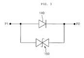
- FIG. 3is a circuit diagram of FIG. 1 ;
- FIG. 4is a sectional view showing a light emitting device package according to a second embodiment
- FIG. 5is a sectional view showing a light emitting device package according to a third embodiment
- FIG. 6is a sectional view showing a light emitting device package according to a fourth embodiment
- FIG. 7is a sectional view showing a light emitting device package according to a fifth embodiment
- FIG. 8is a sectional view showing a light emitting device package according to a sixth embodiment.
- FIG. 9is a sectional view showing a light emitting device package according to a seventh embodiment.
- FIG. 10is a sectional view showing a light emitting device package according to an eighth embodiment.
- each layer shown in the drawingscan be exaggerated, omitted or schematically drawn for the purpose of convenience or clarity.
- the size of elementsdoes not utterly reflect an actual size.
- FIG. 1is a perspective view showing a light emitting device package 100 according to a first embodiment
- FIG. 2is a sectional view taken along line A-A of FIG. 1
- the light emitting device package 100includes a package body 110 , insulating layers 120 and 125 , a reflective layer 130 , a light emitting device 140 , a first electrode 151 , and a second electrode 155 .
- the package body 110may be formed in a wafer level package (WLP) including silicon.
- WLPwafer level package
- a cavity 105 having a predetermined depthis formed at an upper portion of the package body 110 .
- the cavity 105may have one of a bathtub shape, a polygonal shape, and a circular shape.
- a side surface 104 forming the cavity 105is inclined outward from an axis perpendicular to a bottom surface at a predetermined angle.
- the package body 110is shown in a single chip unit, the package body 110 is manufactured on a silicon wafer in the form of a matrix and then cut away from the silicon wafer.
- An outer surface 101 of the package body 110may be a non-inclined surface.
- the package body 110is not connected with a metallic layer through the outer surface 101 , but connected with the metallic layer through a via. Accordingly, the use amount of metal can be reduced.
- the insulating layers 120 and 125are formed on top and bottom surfaces of the package body 110 , respectively.
- the insulating layers 120 and 125may include various insulating materials such as an oxide layer, a silicon thermal oxide layer, AlN, SiC, alumina, and a silicon nitride, but the embodiment is not limited thereto.
- the first and second electrodes 151 and 155connect a rear surface of the package body 110 with the cavity 105 through a via structure.
- the first electrode 151includes a first upper electrode 152 , a first via electrode 153 , and a first lower electrode 154
- the second electrode 155includes a second upper electrode 156 , a second via electrode 157 , and a second lower electrode 158 .
- the first and second upper electrodes 152 and 156are spaced apart from each other in the cavity area 105 in which the light emitting device 140 is installed.
- One end of the first via electrode 153is connected with the first upper electrode 152 , and an opposite end of the via electrode 153 is connected with the first lower electrode 154 .
- One end of the second via electrode 157is connected with the second upper electrode 156 , and an opposite end of the second via electrode 157 is connected with the second lower electrode 158 .
- the first and second via electrodes 153 and 157are insulated from the package body 110 by the insulating layer 122 .
- a single via electrode or a plurality of via electrodesmay be formed.
- a via hole 103 in which the first and second via electrodes 153 and 157 are formedmay have a circular column shape or a polygonal column shape.
- the via hole 103may have a predetermined area capable of improving a heat sink efficiency.
- At least one light emitting device 140may be disposed in the cavity 105 of the package body 110 .
- the light emitting device 140may be connected with the first and second upper electrodes 152 and 156 through a flip-chip bonding scheme using a bump.
- the light emitting device 140may include a color LED chip such as a blue, green, red, or yellow LED chip, or an ultraviolet LED chip.
- a color LED chipsuch as a blue, green, red, or yellow LED chip, or an ultraviolet LED chip. The embodiment does not restrict the type or the number of light emitting devices 140 .
- the reflective layer 130is formed on the top surface of the package body 110 .
- the reflective layer 130may have a structure in which first and second media 131 and 132 having different refractive indexes are alternately stacked on each other.
- the first medium 131may include non-metal having a lower refractive index
- the second medium 132may include non-metal having a higher refractive index.
- the first medium 131may include one selected from among Al 2 O 3 , SiO 2 , and Fe 2 O 3 .
- the second medium 132may include TiO 2 .
- the TiO 2causes different indexes according to crystalline directions.
- the reflective layer 130may have a stacked structure of 4 to 15 pairs of the first and second media 131 and 132 .
- the first medium 131may have a thickness of 650 ⁇ to 1300 ⁇
- the second medium 132may have a thickness of 450 ⁇ to 900 ⁇ .
- the thickness of each mediummay be varied depending on light emitting wavelengths of the light emitting device 100 .
- the thickness of the Al 2 O 3is in the range of 680 ⁇ to 730 ⁇
- the thickness of the TiO 2is in the range of 480 ⁇ to 515 ⁇ .
- the thickness of the Al 2 O 3is in the range of 803 ⁇ to 865 ⁇ , and the thickness of the TiO 2 is in the range of 570 ⁇ to 610 ⁇ .
- the thickness of each mediumis in the range of 800 ⁇ to 1200 ⁇ .
- 5 to 10 pairs of Al 2 O 3 /TiO 2may be formed based on light reflectivity.
- the reflective layer 130 having the above structurehas reflectivity higher than that of Ag, so that light reflective efficiency can be improved.
- First and second doped layers 161 and 163may be formed in the package body 110 .
- the first and second doped layers 161 and 163may be selectively formed on a top surface or a bottom surface of the package body 110 .
- the first and second doped layers 161 and 163may be formed by diffusing or implanting impurities having a polarity opposite to that of the package body 110 .
- first and second doped layers 161 and 163are formed on the bottom surface of the package body 110 , the first doped layer 161 may be connected between the package body 110 and the first lower electrode 154 , and the second doped layer 163 may be connected between the package body 110 and the second lower electrode 158 .
- the first and second doped layers 161 and 163may include a zener diode.
- a resin membermay be formed in the cavity 105 .
- the resin membermay include transparent silicon or epoxy. At least one kind of fluorescent substance may be added to the resin member.
- a lensmay be formed over the cavity 105 or the resin member.
- the lensmay include a convex lens or a lens manufactured through a transfer molding scheme.
- FIG. 3is a circuit diagram of the light emitting device package according to the first embodiment.
- the light emitting device 140may be connected with a zener diode 160 in parallel.
- First and second electrodes P 1 and P 2may be connected with both ends of the light emitting device 140 and the zener diode 160 .
- the zener diode 160is represented as a bi-directional zener diode having a bi-directional threshold voltage. However, the zener diode 160 may have various structures, and may be selectively realized in the package body 110 .
- FIG. 4is a sectional view showing a light emitting device package 100 A according to a second embodiment.
- the same reference numeralswill be assigned to elements the same as those of the first embodiment in order to avoid redundancy.
- a light emitting device 141is connected with the first upper electrode 152 of the first electrode 151 through a wire, and connected with the second upper electrode 156 of the second electrode 155 through a wire 143 .
- FIG. 5is a sectional view showing a light emitting device package 100 B according to a third embodiment.
- the same reference numeralswill be assigned to elements the same as those of the first embodiment in order to avoid redundancy.
- a light emitting device 142is connected with a first upper electrode 152 B of the first electrode 151 through die-bonding, and connected with a second upper electrode 156 B of the second electrode 155 through the wire 143 .
- FIG. 6is a sectional view showing a light emitting device package 100 C according to a fourth embodiment.
- the same reference numeralswill be assigned to elements the same as those of the second embodiment in order to avoid redundancy.
- the first and second upper electrodes 152 and 156extend in the package body 110 .
- the first and second upper electrodes 152 and 156are disposed on an inclined surface and an upper portion of the package body 110 , thereby further improving reflective efficiency.
- FIG. 7is a sectional view showing a light emitting device package 100 D according to a fifth embodiment.
- the same reference numeralswill be assigned to elements the same as those of the third embodiment in order to avoid redundancy.
- the first and second upper electrodes 152 B and 156 Bextend in the package body 110 .
- the first and second upper electrodes 152 B and 156 Bare disposed on an inclined surface and an upper portion of the package body 110 , thereby further improving reflective efficiency.
- FIG. 8is a sectional view showing a light emitting device package 100 E according to a sixth embodiment.
- the same reference numeralswill be assigned to elements the same as those of the second embodiment in order to avoid redundancy.
- a via plug 170may be disposed at a lower portion of the package body 110 .
- the via plug 170may include a metallic material. Accordingly, the via plug 170 can discharge heat generated from the light emitting device 141 , so that a heat sink characteristic can be improved.
- FIG. 9is a sectional view showing a light emitting device package 100 F according to a seventh embodiment.
- the same reference numeralswill be assigned to elements the same as those of the second embodiment in order to avoid redundancy.
- inclined surfaces 171are formed at both ends of the package body 110 .
- both ends of the package body 110are not inclined, both ends of the package body 110 according to the previous embodiments may have the inclined surfaces 171 as shown in FIG. 9 .
- FIG. 10is a sectional view showing a light emitting device package 100 G according to an eighth embodiment.
- the same reference numeralswill be assigned to elements the same as those of the second embodiment in order to avoid redundancy.
- the light emitting device package 100 Gmakes a difference from the previous embodiments in that the light emitting device package 100 G includes the package body 110 having a plane shape.
- the package body 110may be realized by using a silicon substrate.
- a molding part 180may be further formed on the light emitting device 141 .
- the molding part 180may be made of resin.
- the molding part 180may be made of transparent silicon or epoxy.
- the molding part 180may include a fluorescent substance.
- the molding part 180may have the shape of a lens.
- the molding part 180may have the shape of a spherical lens or the shape of the aspherical lens.
- first and second upper electrodes 152 and 156may extend to both ends of the package body 110 . Accordingly, the first and second upper electrodes 152 and 156 are formed below the reflective layer 130 , thereby further improving reflective efficiency.
- the above-described light emitting device packageis variously adaptable for a backlight unit, an illumination device, and so on.
- the backlight unitcan be adapted to a display apparatus such as a liquid crystal display to supply light to the display apparatus.
- the backlight unitmay include a light supply part, a light guide plate, and an optical sheet.
- the light emitting device package according to the embodimentscan be adapted to the light supply part.
- the backlight unitmay not employ the light guide plate.
- the illumination devicemay include a case and a light supply module.
- the light supply modulemay be disposed in the case.
- the light emitting device package according to the embodimentscan be adapted to the light supply module.
Landscapes
- Engineering & Computer Science (AREA)
- Microelectronics & Electronic Packaging (AREA)
- Physics & Mathematics (AREA)
- Condensed Matter Physics & Semiconductors (AREA)
- General Physics & Mathematics (AREA)
- Computer Hardware Design (AREA)
- Power Engineering (AREA)
- Led Device Packages (AREA)
Abstract
Description
Claims (16)
Applications Claiming Priority (2)
| Application Number | Priority Date | Filing Date | Title |
|---|---|---|---|
| KR10-2009-0013155 | 2009-02-17 | ||
| KR1020090013155AKR101064026B1 (en) | 2009-02-17 | 2009-02-17 | Light emitting device package and manufacturing method thereof |
Publications (2)
| Publication Number | Publication Date |
|---|---|
| US20100207152A1 US20100207152A1 (en) | 2010-08-19 |
| US8648365B2true US8648365B2 (en) | 2014-02-11 |
Family
ID=42174549
Family Applications (1)
| Application Number | Title | Priority Date | Filing Date |
|---|---|---|---|
| US12/706,431Active2031-07-25US8648365B2 (en) | 2009-02-17 | 2010-02-16 | Lighting emitting device package |
Country Status (4)
| Country | Link |
|---|---|
| US (1) | US8648365B2 (en) |
| EP (1) | EP2219241B1 (en) |
| KR (1) | KR101064026B1 (en) |
| CN (1) | CN101807656A (en) |
Cited By (6)
| Publication number | Priority date | Publication date | Assignee | Title |
|---|---|---|---|---|
| US20150014731A1 (en)* | 2012-02-27 | 2015-01-15 | LG INNOTEK Co,. LTD | Light emitting device package |
| USD778849S1 (en)* | 2015-11-05 | 2017-02-14 | Dowa Electronics Materials Co., Ltd. | Light emitting diode chip |
| USD800678S1 (en)* | 2016-04-28 | 2017-10-24 | Citizen Electronics Co., Ltd. | Light emitting diode |
| US10347806B2 (en)* | 2017-04-12 | 2019-07-09 | Luminus, Inc. | Packaged UV-LED device with anodic bonded silica lens and no UV-degradable adhesive |
| US10388584B2 (en)* | 2011-09-06 | 2019-08-20 | STATS ChipPAC Pte. Ltd. | Semiconductor device and method of forming Fo-WLCSP with recessed interconnect area in peripheral region of semiconductor die |
| US11499684B2 (en)* | 2020-04-13 | 2022-11-15 | Nichia Corporation | Planar light source and the method of manufacturing the same |
Families Citing this family (29)
| Publication number | Priority date | Publication date | Assignee | Title |
|---|---|---|---|---|
| KR101020993B1 (en)* | 2009-03-10 | 2011-03-09 | 엘지이노텍 주식회사 | Light emitting device package and its manufacturing method |
| JP5343831B2 (en)* | 2009-04-16 | 2013-11-13 | 日亜化学工業株式会社 | Light emitting device |
| KR101072212B1 (en)* | 2010-01-05 | 2011-10-10 | 엘지이노텍 주식회사 | Light emitting device and method for fabricating the same |
| KR101124816B1 (en)* | 2010-09-24 | 2012-03-26 | 서울옵토디바이스주식회사 | Light emitting diode package and method of manufacturing thereof |
| DE102010054898A1 (en) | 2010-12-17 | 2012-06-21 | Osram Opto Semiconductors Gmbh | Carrier for an optoelectronic semiconductor chip and semiconductor chip |
| CN102646773B (en)* | 2011-02-17 | 2015-02-04 | 展晶科技(深圳)有限公司 | Light emitting diode (LED) packaging structure and processing procedure |
| DE102011012924A1 (en)* | 2011-03-03 | 2012-09-06 | Osram Opto Semiconductors Gmbh | Support for an optoelectronic structure and optoelectronic semiconductor chip with such a support |
| DE102011103412A1 (en) | 2011-06-06 | 2012-12-06 | Osram Opto Semiconductors Gmbh | Method for producing an optoelectronic semiconductor component and such a semiconductor component |
| DE102011083691B4 (en)* | 2011-09-29 | 2020-03-12 | Osram Gmbh | OPTOELECTRONIC SEMICONDUCTOR COMPONENT |
| DE102012202555A1 (en)* | 2012-02-20 | 2013-08-22 | Osram Gmbh | LED ARRANGEMENT |
| US9389425B2 (en)* | 2012-04-18 | 2016-07-12 | Kopin Corporation | Viewer with display overlay |
| US9323061B2 (en) | 2012-04-18 | 2016-04-26 | Kopin Corporation | Viewer with display overlay |
| EP2879195A4 (en)* | 2012-07-27 | 2016-01-20 | Konica Minolta Inc | LED DEVICE AND METHOD OF MANUFACTURING THE SAME |
| DE102013105631A1 (en)* | 2013-05-31 | 2014-12-04 | Osram Opto Semiconductors Gmbh | Support for an optoelectronic semiconductor chip and optoelectronic component |
| EP3084849B1 (en) | 2013-12-18 | 2019-10-02 | Lumileds Holding B.V. | Reflective solder mask layer for led package and method of fabricating a light emitting structure |
| JP6533066B2 (en)* | 2015-02-18 | 2019-06-19 | ローム株式会社 | Electronic device |
| US10534166B2 (en) | 2016-09-22 | 2020-01-14 | Lightforce Usa, Inc. | Optical targeting information projection system |
| JP7118982B2 (en) | 2017-02-06 | 2022-08-16 | シェルタード ウィングス インコーポレイテッド ドゥーイング ビジネス アズ ヴォルテクス オプティクス | Observation optics with built-in display system |
| US11675180B2 (en) | 2018-01-12 | 2023-06-13 | Sheltered Wings, Inc. | Viewing optic with an integrated display system |
| EP3769028B1 (en) | 2018-03-20 | 2024-06-26 | Sheltered Wings, Inc. D/b/a/ Vortex Optics | Viewing optic with a base having a light module |
| PL3781894T3 (en) | 2018-04-20 | 2025-04-22 | Sheltered Wings, Inc. D/B/A/ Vortex Optics | Viewing optic with direct active reticle targeting |
| KR102701803B1 (en)* | 2018-06-11 | 2024-09-03 | 서울반도체 주식회사 | Light emitting diode package |
| KR102680240B1 (en) | 2018-08-08 | 2024-07-02 | 쉘터드 윙스, 인크. 디/비/에이 보텍스 옵틱스 | Display system for viewing optics |
| CA3127091A1 (en) | 2019-01-18 | 2020-07-23 | Sheltered Wings, Inc. D/B/A Vortex Optics | Viewing optic with round counter system |
| US11561338B2 (en)* | 2019-09-30 | 2023-01-24 | Nichia Corporation | Light-emitting module |
| CN111668233B (en)* | 2020-06-08 | 2023-06-30 | Tcl华星光电技术有限公司 | Display panel and manufacturing method thereof |
| US11430920B2 (en) | 2020-06-08 | 2022-08-30 | Tcl China Star Optoelectronics Technology Co., Ltd. | Display panel and manufacturing method thereof |
| DE102021128151A1 (en)* | 2021-10-28 | 2023-05-04 | OSRAM Opto Semiconductors Gesellschaft mit beschränkter Haftung | METHOD FOR MANUFACTURING OPTOELECTRONIC DEVICE AND OPTOELECTRONIC DEVICE |
| KR20230070097A (en)* | 2021-11-12 | 2023-05-22 | 삼성디스플레이 주식회사 | Display device |
Citations (43)
| Publication number | Priority date | Publication date | Assignee | Title |
|---|---|---|---|---|
| US6184544B1 (en)* | 1998-01-29 | 2001-02-06 | Rohm Co., Ltd. | Semiconductor light emitting device with light reflective current diffusion layer |
| US6531328B1 (en)* | 2001-10-11 | 2003-03-11 | Solidlite Corporation | Packaging of light-emitting diode |
| US20040196877A1 (en)* | 2003-04-01 | 2004-10-07 | Sharp Kabushiki Kaisha | Multi-wavelength laser device |
| US6833566B2 (en)* | 2001-03-28 | 2004-12-21 | Toyoda Gosei Co., Ltd. | Light emitting diode with heat sink |
| KR20050052196A (en)* | 2003-11-29 | 2005-06-02 | 삼성에스디아이 주식회사 | Apparatus for driving plasma display panel comprising protection circuit |
| US20050139846A1 (en) | 2003-12-26 | 2005-06-30 | Park Jung K. | High power light emitting diode package and fabrication method thereof |
| US20060057751A1 (en)* | 2004-09-15 | 2006-03-16 | Yu-Nung Shen | LED package and method for producing the same |
| KR100593937B1 (en) | 2005-03-30 | 2006-06-30 | 삼성전기주식회사 | LED package using Si substrate and manufacturing method thereof |
| US20060198162A1 (en)* | 2003-03-18 | 2006-09-07 | Sumitomo Electric Industries, Ltd. | Light emitting element mounting member, and semiconductor device using the same |
| US20060208271A1 (en)* | 2005-03-21 | 2006-09-21 | Lg Electronics Inc. | Light source apparatus and fabrication method thereof |
| US7129576B2 (en)* | 2003-09-26 | 2006-10-31 | Tessera, Inc. | Structure and method of making capped chips including vertical interconnects having stud bumps engaged to surfaces of said caps |
| US20060261364A1 (en)* | 2003-03-10 | 2006-11-23 | Yoshinobu Suehiro | Solid element device and method for manufacturing thereof |
| US20070090510A1 (en)* | 2005-10-21 | 2007-04-26 | Advanced Optoelectronic Technology Inc. | Package structure for solid-state lighting devices and method of fabricating the same |
| KR20070050159A (en) | 2005-11-10 | 2007-05-15 | 삼성전자주식회사 | High Brightness LED and Liquid Crystal Display Using Same |
| US20070114552A1 (en)* | 2005-11-23 | 2007-05-24 | Samsung Electro-Mechanics Co., Ltd. | Vertical gallium-nitride based light emitting diode |
| KR20070074460A (en) | 2006-01-06 | 2007-07-12 | 신꼬오덴기 고교 가부시키가이샤 | Manufacturing Method of Semiconductor Device |
| US20070164303A1 (en)* | 2006-01-13 | 2007-07-19 | Lightop Technology Co., Ltd. | [led lamp] |
| US20070170454A1 (en)* | 2006-01-20 | 2007-07-26 | Cree, Inc. | Packages for semiconductor light emitting devices utilizing dispensed reflectors and methods of forming the same |
| US20070170448A1 (en)* | 2006-01-24 | 2007-07-26 | Sony Corporation | Semiconductor light emitting device and semiconductor light emitting device assembly |
| US20070194712A1 (en)* | 2006-02-02 | 2007-08-23 | Shinko Electric Industries Co., Ltd. | Semiconductor device and method of manufacturing semiconductor device |
| US20070221928A1 (en)* | 2006-03-14 | 2007-09-27 | Samsung Electro-Mechanics Co., Ltd. | Light emitting diode package |
| US20070246724A1 (en)* | 2006-04-21 | 2007-10-25 | Silicon Base Development Inc. | Package base structure and associated manufacturing method |
| EP1876653A2 (en) | 2006-07-07 | 2008-01-09 | LG Electronics Inc. | Sub-mount for mounting light emitting device and light emitting device package |
| US20080043444A1 (en) | 2004-04-27 | 2008-02-21 | Kyocera Corporation | Wiring Board for Light-Emitting Element |
| WO2008059650A1 (en) | 2006-11-14 | 2008-05-22 | Harison Toshiba Lighting Corp. | Light emitting device, its manufacturing method and its mounted substrate |
| KR20080051877A (en) | 2006-12-07 | 2008-06-11 | 엘지전자 주식회사 | Light emitting device package and its manufacturing method |
| US20080149962A1 (en)* | 2006-12-21 | 2008-06-26 | Lg Electronics Inc. | Light emitting device package and method for manufacturing the same |
| US20080179605A1 (en)* | 2007-01-29 | 2008-07-31 | Yuji Takase | Nitride semiconductor light emitting device and method for fabricating the same |
| US20080185605A1 (en)* | 2007-01-15 | 2008-08-07 | Citizen Electronics Co., Ltd. | Light-emitting diode and method for producing it |
| US20080191227A1 (en)* | 2005-04-01 | 2008-08-14 | Matsushita Electric Industrial Co., Ltd. | Surface-Mount Type Optical Semiconductor Device and Method For Manufacturing Same |
| US20080197370A1 (en)* | 2007-02-16 | 2008-08-21 | Hung-Yi Lin | Light emitting diode structure and manufacturing method thereof |
| US20080212630A1 (en)* | 2007-03-01 | 2008-09-04 | Denso Corporation | Laser apparatus |
| US20080280161A1 (en)* | 2007-05-09 | 2008-11-13 | Samsung Electronics Co., Ltd. | Light emitting diode device using nanocrystal-metal oxide composite and method for fabricating the same |
| US20080315230A1 (en)* | 2007-06-20 | 2008-12-25 | Shinko Electric Industries Co., Ltd. | Electronic component package and method of manufacturing the same, and electronic component device |
| US20090090926A1 (en)* | 2007-10-09 | 2009-04-09 | Foxsemicon Integrated Technology, Inc. | Solid state light emitting device |
| US7518158B2 (en)* | 2003-12-09 | 2009-04-14 | Cree, Inc. | Semiconductor light emitting devices and submounts |
| US20090146155A1 (en)* | 2007-12-11 | 2009-06-11 | Foxsemicon Integrated Technology, Inc. | Light-emitting diode |
| US20090166664A1 (en)* | 2007-12-28 | 2009-07-02 | Samsung Electro-Mechanics Co., Ltd. | High power light emitting diode package and manufacturing method thereof |
| US20090179215A1 (en)* | 2008-01-16 | 2009-07-16 | Rohm Co., Ltd. | Semiconductor light emitting device and fabrication method for the semiconductor light emitting device |
| US20090244740A1 (en)* | 2008-03-31 | 2009-10-01 | Murakami Corporation | Light-emitting display device-equipped rear-view mirror |
| US20090274188A1 (en)* | 2008-05-01 | 2009-11-05 | Samsung Electronics Co., Ltd. | Light emitting device and fabrication method thereof |
| US7956379B2 (en)* | 2009-06-10 | 2011-06-07 | Lg Innotek Co., Ltd. | Light emitting device, method of manufacturing the same, light emitting device package, and lighting system |
| US7981798B2 (en)* | 2007-09-21 | 2011-07-19 | Shinko Electric Industries Co., Ltd. | Method of manufacturing substrate |
- 2009
- 2009-02-17KRKR1020090013155Apatent/KR101064026B1/ennot_activeExpired - Fee Related
- 2010
- 2010-02-16USUS12/706,431patent/US8648365B2/enactiveActive
- 2010-02-17EPEP10153792.6Apatent/EP2219241B1/enactiveActive
- 2010-02-20CNCN201010121526Apatent/CN101807656A/enactivePending
Patent Citations (52)
| Publication number | Priority date | Publication date | Assignee | Title |
|---|---|---|---|---|
| US6184544B1 (en)* | 1998-01-29 | 2001-02-06 | Rohm Co., Ltd. | Semiconductor light emitting device with light reflective current diffusion layer |
| US6833566B2 (en)* | 2001-03-28 | 2004-12-21 | Toyoda Gosei Co., Ltd. | Light emitting diode with heat sink |
| US6531328B1 (en)* | 2001-10-11 | 2003-03-11 | Solidlite Corporation | Packaging of light-emitting diode |
| US20060261364A1 (en)* | 2003-03-10 | 2006-11-23 | Yoshinobu Suehiro | Solid element device and method for manufacturing thereof |
| US20060198162A1 (en)* | 2003-03-18 | 2006-09-07 | Sumitomo Electric Industries, Ltd. | Light emitting element mounting member, and semiconductor device using the same |
| US20040196877A1 (en)* | 2003-04-01 | 2004-10-07 | Sharp Kabushiki Kaisha | Multi-wavelength laser device |
| US7129576B2 (en)* | 2003-09-26 | 2006-10-31 | Tessera, Inc. | Structure and method of making capped chips including vertical interconnects having stud bumps engaged to surfaces of said caps |
| KR20050052196A (en)* | 2003-11-29 | 2005-06-02 | 삼성에스디아이 주식회사 | Apparatus for driving plasma display panel comprising protection circuit |
| US7518158B2 (en)* | 2003-12-09 | 2009-04-14 | Cree, Inc. | Semiconductor light emitting devices and submounts |
| US20050139846A1 (en) | 2003-12-26 | 2005-06-30 | Park Jung K. | High power light emitting diode package and fabrication method thereof |
| US20080043444A1 (en) | 2004-04-27 | 2008-02-21 | Kyocera Corporation | Wiring Board for Light-Emitting Element |
| US20060057751A1 (en)* | 2004-09-15 | 2006-03-16 | Yu-Nung Shen | LED package and method for producing the same |
| US20060208271A1 (en)* | 2005-03-21 | 2006-09-21 | Lg Electronics Inc. | Light source apparatus and fabrication method thereof |
| US20060220036A1 (en)* | 2005-03-30 | 2006-10-05 | Samsung Electro-Mechanics Co., Ltd. | LED package using Si substrate and fabricating method thereof |
| KR100593937B1 (en) | 2005-03-30 | 2006-06-30 | 삼성전기주식회사 | LED package using Si substrate and manufacturing method thereof |
| US20080191227A1 (en)* | 2005-04-01 | 2008-08-14 | Matsushita Electric Industrial Co., Ltd. | Surface-Mount Type Optical Semiconductor Device and Method For Manufacturing Same |
| US20070090510A1 (en)* | 2005-10-21 | 2007-04-26 | Advanced Optoelectronic Technology Inc. | Package structure for solid-state lighting devices and method of fabricating the same |
| US7719099B2 (en)* | 2005-10-21 | 2010-05-18 | Advanced Optoelectronic Technology Inc. | Package structure for solid-state lighting devices and method of fabricating the same |
| KR20070050159A (en) | 2005-11-10 | 2007-05-15 | 삼성전자주식회사 | High Brightness LED and Liquid Crystal Display Using Same |
| US20070145383A1 (en) | 2005-11-10 | 2007-06-28 | Samsung Electronics Co., Ltd. | High luminance light emitting diode and liquid crystal display device using the same |
| US7372078B2 (en)* | 2005-11-23 | 2008-05-13 | Samsung Electro-Mechanics Co., Ltd. | Vertical gallium-nitride based light emitting diode |
| US20070114552A1 (en)* | 2005-11-23 | 2007-05-24 | Samsung Electro-Mechanics Co., Ltd. | Vertical gallium-nitride based light emitting diode |
| US20070161211A1 (en)* | 2006-01-06 | 2007-07-12 | Masahiro Sunohara | Method for manufacturing semiconductor device |
| KR20070074460A (en) | 2006-01-06 | 2007-07-12 | 신꼬오덴기 고교 가부시키가이샤 | Manufacturing Method of Semiconductor Device |
| US20070164303A1 (en)* | 2006-01-13 | 2007-07-19 | Lightop Technology Co., Ltd. | [led lamp] |
| US20070170454A1 (en)* | 2006-01-20 | 2007-07-26 | Cree, Inc. | Packages for semiconductor light emitting devices utilizing dispensed reflectors and methods of forming the same |
| US20070170448A1 (en)* | 2006-01-24 | 2007-07-26 | Sony Corporation | Semiconductor light emitting device and semiconductor light emitting device assembly |
| US20070194712A1 (en)* | 2006-02-02 | 2007-08-23 | Shinko Electric Industries Co., Ltd. | Semiconductor device and method of manufacturing semiconductor device |
| US20070221928A1 (en)* | 2006-03-14 | 2007-09-27 | Samsung Electro-Mechanics Co., Ltd. | Light emitting diode package |
| US20070246724A1 (en)* | 2006-04-21 | 2007-10-25 | Silicon Base Development Inc. | Package base structure and associated manufacturing method |
| US8048694B2 (en)* | 2006-04-21 | 2011-11-01 | Silicon Base Development Inc. | Package base structure and associated manufacturing method |
| EP1876653A2 (en) | 2006-07-07 | 2008-01-09 | LG Electronics Inc. | Sub-mount for mounting light emitting device and light emitting device package |
| US7714341B2 (en)* | 2006-07-07 | 2010-05-11 | Lg Innotek Co., Ltd. | Sub-mount for mounting light emitting device and light emitting device package |
| US20080006837A1 (en) | 2006-07-07 | 2008-01-10 | Lg Electronics Inc. And Lg Innotek Co., Ltd | Sub-mount for mounting light emitting device and light emitting device package |
| WO2008059650A1 (en) | 2006-11-14 | 2008-05-22 | Harison Toshiba Lighting Corp. | Light emitting device, its manufacturing method and its mounted substrate |
| KR20080051877A (en) | 2006-12-07 | 2008-06-11 | 엘지전자 주식회사 | Light emitting device package and its manufacturing method |
| US20080149962A1 (en)* | 2006-12-21 | 2008-06-26 | Lg Electronics Inc. | Light emitting device package and method for manufacturing the same |
| US20080185605A1 (en)* | 2007-01-15 | 2008-08-07 | Citizen Electronics Co., Ltd. | Light-emitting diode and method for producing it |
| US20080179605A1 (en)* | 2007-01-29 | 2008-07-31 | Yuji Takase | Nitride semiconductor light emitting device and method for fabricating the same |
| US20080197370A1 (en)* | 2007-02-16 | 2008-08-21 | Hung-Yi Lin | Light emitting diode structure and manufacturing method thereof |
| US20090032832A1 (en)* | 2007-02-16 | 2009-02-05 | Hung-Yi Lin | Light emitting diode structure |
| US20080212630A1 (en)* | 2007-03-01 | 2008-09-04 | Denso Corporation | Laser apparatus |
| US20080280161A1 (en)* | 2007-05-09 | 2008-11-13 | Samsung Electronics Co., Ltd. | Light emitting diode device using nanocrystal-metal oxide composite and method for fabricating the same |
| US20080315230A1 (en)* | 2007-06-20 | 2008-12-25 | Shinko Electric Industries Co., Ltd. | Electronic component package and method of manufacturing the same, and electronic component device |
| US7981798B2 (en)* | 2007-09-21 | 2011-07-19 | Shinko Electric Industries Co., Ltd. | Method of manufacturing substrate |
| US20090090926A1 (en)* | 2007-10-09 | 2009-04-09 | Foxsemicon Integrated Technology, Inc. | Solid state light emitting device |
| US20090146155A1 (en)* | 2007-12-11 | 2009-06-11 | Foxsemicon Integrated Technology, Inc. | Light-emitting diode |
| US20090166664A1 (en)* | 2007-12-28 | 2009-07-02 | Samsung Electro-Mechanics Co., Ltd. | High power light emitting diode package and manufacturing method thereof |
| US20090179215A1 (en)* | 2008-01-16 | 2009-07-16 | Rohm Co., Ltd. | Semiconductor light emitting device and fabrication method for the semiconductor light emitting device |
| US20090244740A1 (en)* | 2008-03-31 | 2009-10-01 | Murakami Corporation | Light-emitting display device-equipped rear-view mirror |
| US20090274188A1 (en)* | 2008-05-01 | 2009-11-05 | Samsung Electronics Co., Ltd. | Light emitting device and fabrication method thereof |
| US7956379B2 (en)* | 2009-06-10 | 2011-06-07 | Lg Innotek Co., Ltd. | Light emitting device, method of manufacturing the same, light emitting device package, and lighting system |
Cited By (8)
| Publication number | Priority date | Publication date | Assignee | Title |
|---|---|---|---|---|
| US10388584B2 (en)* | 2011-09-06 | 2019-08-20 | STATS ChipPAC Pte. Ltd. | Semiconductor device and method of forming Fo-WLCSP with recessed interconnect area in peripheral region of semiconductor die |
| US20150014731A1 (en)* | 2012-02-27 | 2015-01-15 | LG INNOTEK Co,. LTD | Light emitting device package |
| US9293672B2 (en)* | 2012-02-27 | 2016-03-22 | Lg Innotek Co., Ltd. | Light emitting device package |
| USD778849S1 (en)* | 2015-11-05 | 2017-02-14 | Dowa Electronics Materials Co., Ltd. | Light emitting diode chip |
| USD800678S1 (en)* | 2016-04-28 | 2017-10-24 | Citizen Electronics Co., Ltd. | Light emitting diode |
| US10347806B2 (en)* | 2017-04-12 | 2019-07-09 | Luminus, Inc. | Packaged UV-LED device with anodic bonded silica lens and no UV-degradable adhesive |
| US11499684B2 (en)* | 2020-04-13 | 2022-11-15 | Nichia Corporation | Planar light source and the method of manufacturing the same |
| US12111024B2 (en) | 2020-04-13 | 2024-10-08 | Nichia Corporation | Planar light source and the method of manufacturing the same |
Also Published As
| Publication number | Publication date |
|---|---|
| KR20100093975A (en) | 2010-08-26 |
| EP2219241A1 (en) | 2010-08-18 |
| US20100207152A1 (en) | 2010-08-19 |
| EP2219241B1 (en) | 2019-06-19 |
| KR101064026B1 (en) | 2011-09-08 |
| CN101807656A (en) | 2010-08-18 |
Similar Documents
| Publication | Publication Date | Title |
|---|---|---|
| US8648365B2 (en) | Lighting emitting device package | |
| JP6437154B2 (en) | Light emitting device package | |
| JP6312899B2 (en) | Light emitting device package, light source module, and illumination system including the same | |
| US8916887B2 (en) | Light emitting device package and lighting system using the same | |
| US9112129B2 (en) | Light emitting diode package and light unit having the same | |
| US8283691B2 (en) | Light emitting device package and a lighting device | |
| US9224926B2 (en) | Light-emitting device and lighting system | |
| US8357948B2 (en) | Light emitting device and lighting system | |
| KR20120122048A (en) | Light emitting device package | |
| KR101170407B1 (en) | Light-emitting device with inorganic housing | |
| KR100667504B1 (en) | Package of light emitting device and manufacturing method thereof | |
| US20100213497A1 (en) | Light emitting device package and lighting system including the same | |
| KR101849126B1 (en) | Light Emitting Device Package | |
| KR102142718B1 (en) | Light emitting device and light apparatus having thereof | |
| KR101904263B1 (en) | Light Emitting Device Package | |
| KR20100119365A (en) | Light emitting diode package | |
| KR101807111B1 (en) | Light emitting device and fabrication method thereof | |
| KR20140015958A (en) | Light emitting device package | |
| KR102098848B1 (en) | Light emitting device package | |
| KR20120073929A (en) | Light emitting device package | |
| KR20150007735A (en) | Light Emitting Diode Package | |
| KR20140094137A (en) | Light emitting device package and backlight unit thereof | |
| KR20140099683A (en) | Light Emitting Devices package |
Legal Events
| Date | Code | Title | Description |
|---|---|---|---|
| AS | Assignment | Owner name:LG INNOTEK CO., LTD., KOREA, REPUBLIC OF Free format text:ASSIGNMENT OF ASSIGNORS INTEREST;ASSIGNOR:WON, JUNG MIN;REEL/FRAME:023956/0559 Effective date:20100208 | |
| FEPP | Fee payment procedure | Free format text:PAYOR NUMBER ASSIGNED (ORIGINAL EVENT CODE: ASPN); ENTITY STATUS OF PATENT OWNER: LARGE ENTITY | |
| STCF | Information on status: patent grant | Free format text:PATENTED CASE | |
| FPAY | Fee payment | Year of fee payment:4 | |
| AS | Assignment | Owner name:SUZHOU LEKIN SEMICONDUCTOR CO., LTD., CHINA Free format text:ASSIGNMENT OF ASSIGNORS INTEREST;ASSIGNOR:LG INNOTEK CO., LTD.;REEL/FRAME:056366/0335 Effective date:20210520 | |
| MAFP | Maintenance fee payment | Free format text:PAYMENT OF MAINTENANCE FEE, 8TH YEAR, LARGE ENTITY (ORIGINAL EVENT CODE: M1552); ENTITY STATUS OF PATENT OWNER: LARGE ENTITY Year of fee payment:8 | |
| FEPP | Fee payment procedure | Free format text:MAINTENANCE FEE REMINDER MAILED (ORIGINAL EVENT CODE: REM.); ENTITY STATUS OF PATENT OWNER: LARGE ENTITY |