US8647981B1 - Methods of forming patterns, and methods of forming integrated circuitry - Google Patents
Methods of forming patterns, and methods of forming integrated circuitryDownload PDFInfo
- Publication number
- US8647981B1 US8647981B1US13/600,714US201213600714AUS8647981B1US 8647981 B1US8647981 B1US 8647981B1US 201213600714 AUS201213600714 AUS 201213600714AUS 8647981 B1US8647981 B1US 8647981B1
- Authority
- US
- United States
- Prior art keywords
- lines
- openings
- pattern
- forming
- over
- Prior art date
- Legal status (The legal status is an assumption and is not a legal conclusion. Google has not performed a legal analysis and makes no representation as to the accuracy of the status listed.)
- Active
Links
Images


Classifications
- H—ELECTRICITY
- H01—ELECTRIC ELEMENTS
- H01L—SEMICONDUCTOR DEVICES NOT COVERED BY CLASS H10
- H01L21/00—Processes or apparatus adapted for the manufacture or treatment of semiconductor or solid state devices or of parts thereof
- H01L21/70—Manufacture or treatment of devices consisting of a plurality of solid state components formed in or on a common substrate or of parts thereof; Manufacture of integrated circuit devices or of parts thereof
- H01L21/71—Manufacture of specific parts of devices defined in group H01L21/70
- H01L21/768—Applying interconnections to be used for carrying current between separate components within a device comprising conductors and dielectrics
- H01L21/76801—Applying interconnections to be used for carrying current between separate components within a device comprising conductors and dielectrics characterised by the formation and the after-treatment of the dielectrics, e.g. smoothing
- H01L21/76802—Applying interconnections to be used for carrying current between separate components within a device comprising conductors and dielectrics characterised by the formation and the after-treatment of the dielectrics, e.g. smoothing by forming openings in dielectrics
- H01L21/76805—Applying interconnections to be used for carrying current between separate components within a device comprising conductors and dielectrics characterised by the formation and the after-treatment of the dielectrics, e.g. smoothing by forming openings in dielectrics the opening being a via or contact hole penetrating the underlying conductor
- H—ELECTRICITY
- H01—ELECTRIC ELEMENTS
- H01L—SEMICONDUCTOR DEVICES NOT COVERED BY CLASS H10
- H01L21/00—Processes or apparatus adapted for the manufacture or treatment of semiconductor or solid state devices or of parts thereof
- H01L21/02—Manufacture or treatment of semiconductor devices or of parts thereof
- H01L21/027—Making masks on semiconductor bodies for further photolithographic processing not provided for in group H01L21/18 or H01L21/34
- H01L21/033—Making masks on semiconductor bodies for further photolithographic processing not provided for in group H01L21/18 or H01L21/34 comprising inorganic layers
- H01L21/0334—Making masks on semiconductor bodies for further photolithographic processing not provided for in group H01L21/18 or H01L21/34 comprising inorganic layers characterised by their size, orientation, disposition, behaviour, shape, in horizontal or vertical plane
- H01L21/0337—Making masks on semiconductor bodies for further photolithographic processing not provided for in group H01L21/18 or H01L21/34 comprising inorganic layers characterised by their size, orientation, disposition, behaviour, shape, in horizontal or vertical plane characterised by the process involved to create the mask, e.g. lift-off masks, sidewalls, or to modify the mask, e.g. pre-treatment, post-treatment
- H—ELECTRICITY
- H01—ELECTRIC ELEMENTS
- H01L—SEMICONDUCTOR DEVICES NOT COVERED BY CLASS H10
- H01L21/00—Processes or apparatus adapted for the manufacture or treatment of semiconductor or solid state devices or of parts thereof
- H01L21/02—Manufacture or treatment of semiconductor devices or of parts thereof
- H01L21/027—Making masks on semiconductor bodies for further photolithographic processing not provided for in group H01L21/18 or H01L21/34
- H01L21/033—Making masks on semiconductor bodies for further photolithographic processing not provided for in group H01L21/18 or H01L21/34 comprising inorganic layers
- H01L21/0334—Making masks on semiconductor bodies for further photolithographic processing not provided for in group H01L21/18 or H01L21/34 comprising inorganic layers characterised by their size, orientation, disposition, behaviour, shape, in horizontal or vertical plane
- H01L21/0338—Process specially adapted to improve the resolution of the mask
- H—ELECTRICITY
- H01—ELECTRIC ELEMENTS
- H01L—SEMICONDUCTOR DEVICES NOT COVERED BY CLASS H10
- H01L21/00—Processes or apparatus adapted for the manufacture or treatment of semiconductor or solid state devices or of parts thereof
- H01L21/02—Manufacture or treatment of semiconductor devices or of parts thereof
- H01L21/04—Manufacture or treatment of semiconductor devices or of parts thereof the devices having potential barriers, e.g. a PN junction, depletion layer or carrier concentration layer
- H01L21/18—Manufacture or treatment of semiconductor devices or of parts thereof the devices having potential barriers, e.g. a PN junction, depletion layer or carrier concentration layer the devices having semiconductor bodies comprising elements of Group IV of the Periodic Table or AIIIBV compounds with or without impurities, e.g. doping materials
- H01L21/26—Bombardment with radiation
- H01L21/263—Bombardment with radiation with high-energy radiation
- H01L21/265—Bombardment with radiation with high-energy radiation producing ion implantation
- H01L21/266—Bombardment with radiation with high-energy radiation producing ion implantation using masks
- H—ELECTRICITY
- H01—ELECTRIC ELEMENTS
- H01L—SEMICONDUCTOR DEVICES NOT COVERED BY CLASS H10
- H01L21/00—Processes or apparatus adapted for the manufacture or treatment of semiconductor or solid state devices or of parts thereof
- H01L21/02—Manufacture or treatment of semiconductor devices or of parts thereof
- H01L21/04—Manufacture or treatment of semiconductor devices or of parts thereof the devices having potential barriers, e.g. a PN junction, depletion layer or carrier concentration layer
- H01L21/18—Manufacture or treatment of semiconductor devices or of parts thereof the devices having potential barriers, e.g. a PN junction, depletion layer or carrier concentration layer the devices having semiconductor bodies comprising elements of Group IV of the Periodic Table or AIIIBV compounds with or without impurities, e.g. doping materials
- H01L21/30—Treatment of semiconductor bodies using processes or apparatus not provided for in groups H01L21/20 - H01L21/26
- H01L21/302—Treatment of semiconductor bodies using processes or apparatus not provided for in groups H01L21/20 - H01L21/26 to change their surface-physical characteristics or shape, e.g. etching, polishing, cutting
- H01L21/306—Chemical or electrical treatment, e.g. electrolytic etching
- H01L21/308—Chemical or electrical treatment, e.g. electrolytic etching using masks
- H01L21/3083—Chemical or electrical treatment, e.g. electrolytic etching using masks characterised by their size, orientation, disposition, behaviour, shape, in horizontal or vertical plane
- H01L21/3086—Chemical or electrical treatment, e.g. electrolytic etching using masks characterised by their size, orientation, disposition, behaviour, shape, in horizontal or vertical plane characterised by the process involved to create the mask, e.g. lift-off masks, sidewalls, or to modify the mask, e.g. pre-treatment, post-treatment
- H—ELECTRICITY
- H01—ELECTRIC ELEMENTS
- H01L—SEMICONDUCTOR DEVICES NOT COVERED BY CLASS H10
- H01L21/00—Processes or apparatus adapted for the manufacture or treatment of semiconductor or solid state devices or of parts thereof
- H01L21/02—Manufacture or treatment of semiconductor devices or of parts thereof
- H01L21/04—Manufacture or treatment of semiconductor devices or of parts thereof the devices having potential barriers, e.g. a PN junction, depletion layer or carrier concentration layer
- H01L21/18—Manufacture or treatment of semiconductor devices or of parts thereof the devices having potential barriers, e.g. a PN junction, depletion layer or carrier concentration layer the devices having semiconductor bodies comprising elements of Group IV of the Periodic Table or AIIIBV compounds with or without impurities, e.g. doping materials
- H01L21/30—Treatment of semiconductor bodies using processes or apparatus not provided for in groups H01L21/20 - H01L21/26
- H01L21/302—Treatment of semiconductor bodies using processes or apparatus not provided for in groups H01L21/20 - H01L21/26 to change their surface-physical characteristics or shape, e.g. etching, polishing, cutting
- H01L21/306—Chemical or electrical treatment, e.g. electrolytic etching
- H01L21/308—Chemical or electrical treatment, e.g. electrolytic etching using masks
- H01L21/3083—Chemical or electrical treatment, e.g. electrolytic etching using masks characterised by their size, orientation, disposition, behaviour, shape, in horizontal or vertical plane
- H01L21/3088—Process specially adapted to improve the resolution of the mask
- H—ELECTRICITY
- H01—ELECTRIC ELEMENTS
- H01L—SEMICONDUCTOR DEVICES NOT COVERED BY CLASS H10
- H01L21/00—Processes or apparatus adapted for the manufacture or treatment of semiconductor or solid state devices or of parts thereof
- H01L21/02—Manufacture or treatment of semiconductor devices or of parts thereof
- H01L21/04—Manufacture or treatment of semiconductor devices or of parts thereof the devices having potential barriers, e.g. a PN junction, depletion layer or carrier concentration layer
- H01L21/18—Manufacture or treatment of semiconductor devices or of parts thereof the devices having potential barriers, e.g. a PN junction, depletion layer or carrier concentration layer the devices having semiconductor bodies comprising elements of Group IV of the Periodic Table or AIIIBV compounds with or without impurities, e.g. doping materials
- H01L21/30—Treatment of semiconductor bodies using processes or apparatus not provided for in groups H01L21/20 - H01L21/26
- H01L21/31—Treatment of semiconductor bodies using processes or apparatus not provided for in groups H01L21/20 - H01L21/26 to form insulating layers thereon, e.g. for masking or by using photolithographic techniques; After treatment of these layers; Selection of materials for these layers
- H01L21/3105—After-treatment
- H01L21/311—Etching the insulating layers by chemical or physical means
- H01L21/31144—Etching the insulating layers by chemical or physical means using masks
- H—ELECTRICITY
- H01—ELECTRIC ELEMENTS
- H01L—SEMICONDUCTOR DEVICES NOT COVERED BY CLASS H10
- H01L21/00—Processes or apparatus adapted for the manufacture or treatment of semiconductor or solid state devices or of parts thereof
- H01L21/02—Manufacture or treatment of semiconductor devices or of parts thereof
- H01L21/04—Manufacture or treatment of semiconductor devices or of parts thereof the devices having potential barriers, e.g. a PN junction, depletion layer or carrier concentration layer
- H01L21/18—Manufacture or treatment of semiconductor devices or of parts thereof the devices having potential barriers, e.g. a PN junction, depletion layer or carrier concentration layer the devices having semiconductor bodies comprising elements of Group IV of the Periodic Table or AIIIBV compounds with or without impurities, e.g. doping materials
- H01L21/30—Treatment of semiconductor bodies using processes or apparatus not provided for in groups H01L21/20 - H01L21/26
- H01L21/31—Treatment of semiconductor bodies using processes or apparatus not provided for in groups H01L21/20 - H01L21/26 to form insulating layers thereon, e.g. for masking or by using photolithographic techniques; After treatment of these layers; Selection of materials for these layers
- H01L21/3205—Deposition of non-insulating-, e.g. conductive- or resistive-, layers on insulating layers; After-treatment of these layers
- H—ELECTRICITY
- H01—ELECTRIC ELEMENTS
- H01L—SEMICONDUCTOR DEVICES NOT COVERED BY CLASS H10
- H01L21/00—Processes or apparatus adapted for the manufacture or treatment of semiconductor or solid state devices or of parts thereof
- H01L21/70—Manufacture or treatment of devices consisting of a plurality of solid state components formed in or on a common substrate or of parts thereof; Manufacture of integrated circuit devices or of parts thereof
- H01L21/71—Manufacture of specific parts of devices defined in group H01L21/70
- H01L21/768—Applying interconnections to be used for carrying current between separate components within a device comprising conductors and dielectrics
- H01L21/76801—Applying interconnections to be used for carrying current between separate components within a device comprising conductors and dielectrics characterised by the formation and the after-treatment of the dielectrics, e.g. smoothing
- H01L21/76802—Applying interconnections to be used for carrying current between separate components within a device comprising conductors and dielectrics characterised by the formation and the after-treatment of the dielectrics, e.g. smoothing by forming openings in dielectrics
- H—ELECTRICITY
- H01—ELECTRIC ELEMENTS
- H01L—SEMICONDUCTOR DEVICES NOT COVERED BY CLASS H10
- H01L2924/00—Indexing scheme for arrangements or methods for connecting or disconnecting semiconductor or solid-state bodies as covered by H01L24/00
- H01L2924/0001—Technical content checked by a classifier
- H01L2924/0002—Not covered by any one of groups H01L24/00, H01L24/00 and H01L2224/00
- H—ELECTRICITY
- H10—SEMICONDUCTOR DEVICES; ELECTRIC SOLID-STATE DEVICES NOT OTHERWISE PROVIDED FOR
- H10B—ELECTRONIC MEMORY DEVICES
- H10B12/00—Dynamic random access memory [DRAM] devices
Definitions
- a continuing goal in semiconductor processingis to reduce the size of individual electronic components, and to thereby enable smaller and denser integrated circuitry. For instance, it can be desired to form memory circuitry (such as DRAM, NAND memory, etc.) to increasingly higher levels of integration.
- memory circuitrysuch as DRAM, NAND memory, etc.
- Pitchcan be used to quantify the density of an integrated circuit pattern.
- Pitchmay be defined as the distance between an identical point in two neighboring features of a repeating pattern.
- Feature size limitations of a lithographic techniquecan set a minimum pitch that can be obtained from the lithographic technique.
- Lithographic processessuch as photolithography, are commonly utilized during semiconductor processing for fabricating integrated structures.
- Lithographic processeshave minimum capable feature sizes, F, which are the smallest feature sizes that can be reasonably formed with the processes.
- Fminimum capable feature sizes
- photolithographymay be limited by factors such as optics and radiation wavelength.
- Pitch multiplicationsuch as pitch-doubling
- Pitch multiplicationis a method for extending the capabilities of lithographic techniques beyond their minimum pitches.
- Pitch multiplicationmay involve forming sub-lithographic features (i.e., features narrower than minimum lithographic resolution) by depositing a material to have a thickness which is less than that of the minimum capable lithographic feature size, F.
- the materialmay be anisotropically etched to form the sub-lithographic features.
- the sub-lithographic featuresmay then be used for integrated circuit fabrication to create higher density circuit patterns than can be achieved with conventional lithographic processing.
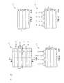
- FIGS. 1-60illustrate a semiconductor construction at various stages of an example embodiment method of forming a pattern.
- FIG. 1shows a top view of the construction
- FIGS. 2-4show cross-sectional side views along the lines A-A, B-B and C-C of FIG. 1 , respectively.
- FIG. 5shows a top view of the construction at a processing stage subsequent to that of FIG. 1 .
- FIGS. 6-8show cross-sectional side views along the lines A-A, B-B and C-C of FIG. 5 , respectively.
- FIG. 9shows a top view of the construction at a processing stage subsequent to that of FIG. 5 .
- FIGS. 10-12show cross-sectional side views along the lines A-A, B-B and C-C of FIG. 9 , respectively.
- FIG. 13shows a top view of the construction at a processing stage subsequent to that of FIG. 9 .
- FIGS. 14-16show cross-sectional side views along the lines A-A, B-B and C-C of FIG. 13 , respectively.
- FIG. 17shows a top view of the construction at a processing stage subsequent to that of FIG. 13 .
- FIGS. 18-20show cross-sectional side views along the lines A-A, B-B and C-C of FIG. 17 , respectively.
- FIG. 21shows a top view of the construction at a processing stage subsequent to that of FIG. 17 .
- FIGS. 22-24show cross-sectional side views along the lines A-A, B-B and C-C of FIG. 21 , respectively.
- FIG. 25shows a top view of the construction at a processing stage subsequent to that of FIG. 21 .
- FIGS. 26-28show cross-sectional side views along the lines A-A, B-B and C-C of FIG. 25 , respectively.
- FIG. 29shows a top view of the construction at a processing stage subsequent to that of FIG. 25 .
- FIGS. 30-32show cross-sectional side views along the lines A-A, B-B and C-C of FIG. 29 , respectively.
- FIG. 33shows a top view of the construction at a processing stage subsequent to that of FIG. 29 .
- FIGS. 34-36show cross-sectional side views along the lines A-A, B-B and C-C of FIG. 33 , respectively.
- FIG. 37shows a top view of the construction at a processing stage subsequent to that of FIG. 33 .
- FIGS. 38-40show cross-sectional side views along the lines A-A, B-B and C-C of FIG. 37 , respectively.
- FIG. 41shows a top view of the construction at a processing stage subsequent to that of FIG. 37 .
- FIGS. 42-44show cross-sectional side views along the lines A-A, B-B and C-C of FIG. 41 , respectively.
- FIG. 45shows a top view of the construction at a processing stage subsequent to that of FIG. 41 .
- FIGS. 46-48show cross-sectional side views along the lines A-A, B-B and C-C of FIG. 45 , respectively.
- FIG. 49shows a top view of the construction at a processing stage subsequent to that of FIG. 45 .
- FIGS. 50-52show cross-sectional side views along the lines A-A, B-B and C-C of FIG. 49 , respectively.
- FIG. 53shows a top view of the construction at a processing stage subsequent to that of FIG. 49 .
- FIGS. 54-56show cross-sectional side views along the lines A-A, B-B and C-C of FIG. 53 , respectively.
- FIG. 57shows a top view of the construction at a processing stage subsequent to that of FIG. 53 .
- FIGS. 58-60show cross-sectional side views along the lines A-A, B-B and C-C of FIG. 57 , respectively.
- FIG. 61shows an expanded view of a region labeled “D” in FIG. 57 .
- FIG. 62shows the construction of FIG. 59 at a processing stage subsequent to that of FIG. 59 in accordance with an example embodiment method.
- FIG. 63shows the construction of FIG. 59 at a processing stage subsequent to that of FIG. 59 in accordance with another example embodiment method.
- Some embodimentscomprise methods of forming patterns in which a second series of lines is overlaid across a first series of lines to form a grid.
- Such gridmay be utilized to define a repeating pattern, and such a pattern may be utilized to fabricate an array of highly-integrated integrated circuitry, such as a DRAM array, a NAND memory array, etc.
- Example embodimentsare described with reference to FIGS. 1-63 .
- a semiconductor construction 10is shown in top view ( FIG. 1 ) and cross-sectional side views ( FIGS. 2-4 ).
- the constructioncomprises a base 12 and a stack 14 of materials 16 , 18 and 20 over the base.
- the basemay comprise, consist essentially of, or consist of monocrystalline silicon, and may be referred to as a semiconductor substrate, or as a portion of a semiconductor substrate.
- semiconductor substratesemiconductor substrate
- semiconductor constructionsemiconductor substrate
- semiconductor substratesemiconductor substrate
- semiconductor substratesemiconductor substrate
- semiconductor substratesemiconductor substrate
- semiconductor material layerssemiconductive material layers
- substraterefers to any supporting structure, including, but not limited to, the semiconductive substrates described above.
- the basemay correspond to a semiconductor substrate containing one or more materials associated with integrated circuit fabrication. In such embodiments, such materials may correspond to one or more of refractory metal materials, barrier materials, diffusion materials, insulator materials, etc.
- the materials 16 , 18 and 20may be selectively etchible relative to one another, and may comprise any suitable materials.
- a first materialis considered to be “selectively etchible” relative to a second material if etching conditions may be chosen which remove the first material at a faster rate than the second material; which can include, but is not limited to, embodiments in which the first material is removed under conditions which are 100 percent selective for the first material relative to the second material.
- material 16may be electrically insulative material which is ultimately patterned into a hard mask suitable for forming an integrated circuit pattern which extends into base 12 (as discussed below with reference to FIG. 63 ).
- material 16may comprise, consist essentially of, or consist of, for example, silicon nitride.
- material 16may be an electrically conductive material which ultimately supports electrically conductive contacts formed thereover (as discussed below with reference to FIG. 62 ).
- material 16may comprise, consist essentially of, or consist of, for example, one or more of various metals (e.g., copper, aluminum, tungsten, titanium, etc.), metal-containing compositions (e.g., metal nitrides, metal carbides, metal silicides, etc.), and conductively-doped semiconductor materials (e.g., conductively-doped silicon, conductively-doped germanium, etc.).
- the material 16may be considered to be an expanse which extends across at least a portion of base 12 .
- material 18may comprise, consist essentially of, or consist of silicon.
- material 18may consist essentially of one or both of polycrystalline silicon and amorphous silicon.
- material 20may comprise silicon oxynitride (e.g., a deposited antireflective composition (DARC)).
- silicon oxynitridee.g., a deposited antireflective composition (DARC)
- the silicon oxynitridemaybe oxygen enriched.
- the materials 16 , 18 and 20may be formed to any suitable thicknesses, and in some embodiments the individual materials may be formed to thicknesses of from about 50 ⁇ to about 1000 ⁇ .
- materials 18 and 20are utilized to form a pattern which is ultimately transferred into one or more structures underlying the materials (for instance, the structures underlying materials 18 and 20 include the material 16 and the base 12 in the shown embodiment).
- materials 18 and 20may be referred to as stacked first and second materials, respectively, which are of different compositions relative to one another.
- Patterned photoresist 22is formed over the stack 14 .
- the patterned photoresistmay be formed utilizing photolithography, and in some embodiments may be referred to as a photolithographically-patterned photoresist mask.
- the patterned photoresistis configured as a plurality of spaced apart lines 24 (which may be referred to as features in some embodiments) extending across an upper surface of material 20 .
- the lines 24extend primarily along a direction of an axis 5 .
- the lines 24are illustrated to be straight, in other embodiments the lines may be curved or wavy.
- the photoresist lines 24are subjected to trimming to reduce widths of the lines.
- the trimming conditionsmay decrease the heights of the lines and/or may induce other changes to the lines (e.g., may impose a dome-shape to the lines).
- trimming conditionsmay be chosen which isotropically etch the lines.
- the trimming of the linesmay be omitted in some embodiments. If the trimming is utilized, such trimming may be accomplished with any suitable processing; including, for example, plasma etching with an inductively coupled reactor.
- the trimmed lines 24 at the processing stage of FIGS. 5-8may have sub-lithographic widths.
- the initial photoresist lines 24 formed at the processing stage of FIGS. 1-4have widths of at least about 40 nanometers (nm), and the trimmed lines 24 at the processing stage of FIGS. 5-8 have widths of less than 40 nm, less than 20 nm, etc.
- the pattern of trimmed photoresist lines 24( FIGS. 5-8 ) is transferred into material 20 , and subsequently the photoresist lines are removed.
- the patterning of material 20forms material 20 into a series of lines 26 over an upper surface of material 18 , with the individual lines extending along the direction of axis 5 .
- the lines 26are spaced-apart from one another by spaces 28 .
- the lines 26 and spaces 28together define an undulating topography of construction 10 .
- a material 30is formed across the undulating topography of lines 26 and spaces 28 .
- the material 30may be a spin-on material, and may be deposited to a suitable thickness and under appropriate conditions to form the shown planarized surface 31 above lines 26 .
- material 30may comprise one or more organic polymers, and accordingly may be a carbon-containing spin-on material.
- material 30may comprise other compositions besides spin-on compositions, and the planarized surface 31 may be formed by chemical-mechanical polishing (CMP) or other suitable planarization.
- CMPchemical-mechanical polishing
- material 30may be referred to as a third material to distinguish it from the above-discussed first and second materials 18 and 20 . In some embodiments, material 30 may be about twice as thick as material 20 .
- a hard mask material 32is formed over surface 31 , and patterned photoresist 34 is formed over the hard mask material.
- the patterned photoresistmay be formed utilizing photolithography, and in some embodiments may be referred to as a photolithographically-patterned photoresist mask.
- the patterned photoresistis configured as a plurality of spaced-apart lines 36 (which may be referred to as features in some embodiments) extending across an upper surface of hard mask material 32 . In the shown embodiment, the lines 36 extend primarily along a direction of an axis 7 .
- the axis 7intersects the axis 5 (described above in FIGS. 1-4 ).
- axis 7is substantially orthogonal to axis 5 ; with the term “substantially orthogonal” meaning that the axes are orthogonal to within reasonable tolerances of fabrication and measurement. In other embodiments, axis 7 may not be substantially orthogonal to axis 5 , and accordingly may intersect axis 5 at an angle other than about 90°.
- lines 36are illustrated to be straight, in other embodiments the lines may be curved or wavy.
- the hard mask material 32may comprise any suitable composition or combination of compositions, and in some embodiments may comprise, consist essentially of, or consist of silicon nitride, silicon oxynitride, etc.
- the pattern of photoresist lines 36( FIGS. 13-16 ) is transferred through hard mask material 32 ( FIGS. 13-16 ) and into material 30 , and subsequently the hard mask material and photoresist lines are removed.
- the patterning of material 30forms material 30 into a series of lines 38 extending over lines 26 and across an upper surface of the material 18 , with the individual lines 38 extending along the direction of axis 7 .
- the lines 38may be about twice as tall as the lines 26 .
- the photoresist lines 36may be trimmed with processing analogous to that of FIGS. 5-8 prior to transferring the pattern of the photoresist lines into material 30 . Accordingly, the lines 38 may have sub-lithographic widths at the processing stage of FIGS. 17-20 .
- the lines 38are subjected to trimming to reduce widths of the lines.
- the trimming conditionsmay decrease the heights of the lines and/or may induce other changes to the lines (e.g., may impose a dome-shape to the lines).
- trimming conditionsmay be chosen which isotropically etch the lines.
- the trimming of the linesmay be omitted in some embodiments. If the trimming is utilized, and the lines 38 comprise organic material, such trimming may be accomplished utilizing, for example, plasma etching with an inductively coupled reactor.
- the lines 38 at the processing stage of FIGS. 21-24have widths of less than 40 nm, less than 20 nm, etc. In some embodiments, the trimmed lines 38 at the processing stage of FIGS. 21-24 may have sub-lithographic widths. In some embodiments, the trimming shown in FIGS. 21-24 may be omitted. In some embodiments, the photoresist lines 36 of FIGS. 13-16 may be trimmed additionally, or alternatively, to trimming the lines 38 of material 30 .
- the lines 26 of material 20may be referred to as first lines, and the lines 38 of material 30 may be referred to as second lines.
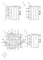
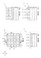
- Such first and second linesform a crosshatch pattern (or lattice) over material 18 .
- Openings 40extend through the crosshatch pattern, with such openings exposing regions of material 18 .
- the first and second lines 26 and 38are both on about the same pitch, P 1 , and are orthogonal to one another. Accordingly, the openings 40 are substantially square. In other embodiments, the lines 38 may be at an angle which is other than orthogonal relative to the lines 26 , and/or the lines 38 may be on a different pitch than the lines 26 . Accordingly, the openings may be rectangular in some embodiments, and may be of other polygonal shapes besides square or rectangular in yet other embodiments. In some embodiments, the lines 26 and/or 38 may be curved or wavy, and thus at least some of the openings may have curved shapes.
- the lines 38have about the same widths as the lines 26 , but in other embodiments the lines 38 may have different widths than the lines 26 . In the shown embodiment, all of the openings 40 are about the same size and shape as one another. However, in some embodiments the lines 26 may be arranged in a pattern other than the shown uniform pitch, and/or the lines 38 may be arranged in a pattern other than the shown uniform pitch, which can enable openings 40 to be formed in a repeating pattern with some of the openings being larger and/or differently shaped than others.
- spacer material 42(only some of which is labeled) is provided along and over the first and second lines 26 and 38 , and then anisotropically etched to form spacers 44 (only some which are labeled).
- the spacersnarrow the openings 40 .
- the spacer material 42may comprise any suitable composition or combination of compositions; and in some embodiments may comprise, consist essentially of, or consist of silicon dioxide or silicon nitride.
- the narrowed openings 40are extended through material 18 to expose an upper surface of material 16 .
- material 18comprises silicon (e.g., polycrystalline and/or amorphous silicon), and material 16 comprise silicon nitride.
- the narrowed openings 40are extended through a silicon-containing material to expose an upper surface of a silicon nitride-containing material.
- material 16may be referred to as an expanse under material 18 , and in such embodiments the narrowed openings may be considered to be extended through material 18 to expose an upper surface of the expanse.
- the openings 40may be extended through material 18 with any suitable processing, including, for example, utilization of a plasma etch.
- the spacers 44are removed with an etch selective for the spacer material 42 ( FIGS. 29-32 ) relative to materials 16 , 18 , 20 and 30 .
- a first materialis considered to be “selectively removed” relative to a second material if the first material is removed at a faster rate than the second material; which can include, but is not limited to, embodiments in which the first material is removed under conditions which are 100 percent selective for the first material relative to the second material.
- the spacer materialconsists of silicon dioxide
- material 16consists of silicon nitride
- material 18consists of silicon
- material 20consists of silicon oxynitride
- material 30consists of an organic polymer.
- exposed portions of material 20are removed selectively relative to material 16 , 18 and 30 . Such removes portions of lines 26 ( FIGS. 33-36 ) while leaving segments 48 of the lines 26 underneath the lines 38 of material 30 .
- the cross-section of FIG. 40shows some segments 48 of lines 26 under one of the lines 38 of material 30 .
- the lines 38 of material 30are removed to uncover the segments 48 of material 20 .
- the segments 48are pedestals having about the same dimensions as openings 40 . In other embodiments, the pedestals may have other dimensions and/or shapes than openings 40 .
- FIG. 41shows that the segments 48 (i.e., the segments of material 20 ) and the openings 40 together form a repeating pattern across the construction 10 .
- the processing of FIGS. 45-60aligns openings in material 18 to the locations of the segments 48 .
- a masking material 50is formed between the segments 48 .
- the masking materialfills the openings 40 , and leaves upper surfaces of the segments 48 exposed.
- the material 50comprises a composition to which material 20 may be selectively removed, and may comprise any suitable substance.
- the masking material 50may comprise a spin-on carbon-containing material, and may be identical to the material 30 described above with reference to FIGS. 13-16 .
- the material 50may be formed in the shown configuration by initially forming material 50 to cover the segments 48 , and then utilizing CMP or other suitable planarization to remove excess material 50 from over the segments 48 ; and/or utilizing a plasma etch to remove the excess material 50 .
- the segments 48are removed selectively relative to material 50 to leave openings 52 extending through material 50 to an upper surface of material 18 .
- the openings 52are extended through material 18 to an upper surface of material 16 .
- the openings 52may be extended through material 18 with any suitable processing, including, for example, utilization of a plasma etch.
- the masking material 50( FIGS. 53-56 ) is removed.
- the remaining material 18is a patterned mask 60 having openings 40 and 52 extending therethrough.
- the openings 40 and 52may be referred to as first and second openings, respectively.
- such first and second openingsare about the same size and shape as one another, but in other embodiments the second openings may be different sizes and/or shapes than the first openings.
- the first and second openingsare approximately square-shaped.
- the openingsmay have other shapes, including rectangular shapes, other polygonal shapes, circular shapes, elliptical shapes, other curved shapes, etc.
- the first openings 40are all approximately the same size and shape as one another. As discussed above with reference to FIGS. 21-24 , in other embodiments some of the openings 40 may be of different size and/or shapes relative to others of such openings.
- the patterned mask 60may comprise the dense repeating pattern illustrated in FIGS. 57-60 , or may comprise other patterns in other embodiments.
- the pattern of openings 40 and 52 of FIGS. 57-60may be considered to be suitable for fabrication of a cross-point array of integrated structures. Such pattern may be tailored for particular applications by adjusting various aspects of the pattern including, for example, sizes of the openings, shapes of the openings, spacings between the openings, pitch regularity, etc.
- FIG. 61shows an expanded region “D” of FIG. 57 and shows that the illustrated dense pattern of mask 60 may have a pitch P 2 which is reduced relative to the pitch P 1 of the lines 26 and 38 of FIGS. 21-24 .
- the pitch P 2is reduced relative to P 1 by a factor of about ⁇ square root over (2) ⁇ .
- the patterned mask 60may be utilized for patterning integrated circuitry.
- FIG. 62shows a construction 10 a at a processing stage subsequent to that of FIG. 59 .
- the construction 10 acomprises electrically conductive material 16
- the mask 60is utilized for patterning a material 70 into electrically conductive interconnects that extend to the conductive material 16 .
- FIG. 63shows a construction 10 b at a processing stage subsequent to that of FIG. 59 in which the openings 40 are extended through material 16 to upper surface of base 12 .
- one or more materialsmay be formed within openings 40 during fabrication of integrated circuitry supported by base 12 , and/or openings 40 may be extended into one or more materials of base 12 , and/or one or more dopants may be implanted through openings 40 and into base 12 .
- the patterned mask 60may be utilized for fabricating one or more components of highly-integrated memory circuitry; such as, for example, DRAM, NAND memory, etc.
- Some embodimentsinclude a method of forming a pattern.
- a series of first linesare formed over a first material.
- a series of second linesare formed over the first lines.
- the first and second linesform a crosshatch pattern over the first material. Regions of the first material are exposed within first openings in the crosshatch pattern.
- the first openingsare extended through the first material. Portions of the first lines that are not covered by the second lines are removed to pattern the first lines into segments.
- the second linesare removed to uncover the segments.
- Masking materialis formed between the segments.
- the masking materialfills the first openings.
- the segmentsare removed to form second openings extending through the masking material to the first material.
- the second openingsare extended through the first material.
- the masking materialis removed to leave a patterned mask comprising the first material having the first and second openings therein.
- Some embodimentsinclude a method of forming a pattern. Stacked first and second materials are formed over a base. The first and second materials are of different compositions relative to one another. The second material is over the first material. The second material is patterned into spaced-apart first lines extending primarily along a first direction. The first lines and spaces between the first lines define an undulating topography. A third material is formed over the undulating topography. The third material has a substantially planar upper surface. The third material is patterned into spaced-apart second lines extending primarily along a second direction that intersects the first direction. The first and second lines form a crosshatch pattern over the first material. Regions of the first material are exposed within first openings in the crosshatch pattern.
- Spacersare formed along sidewalls of the first and second lines to narrow the first openings in the crosshatch pattern.
- the narrowed first openingsare extended through the first material.
- the spacersare removed. Portions of the first lines that are not covered by the second lines are removed to pattern the first lines into segments.
- the second linesare removed to uncover the segments.
- Masking materialis formed between the segments. The masking material fills the narrowed first openings.
- the segmentsare removed to form second openings that extend through the masking material to the first material.
- the second openingsare extended through the first material.
- the masking materialis removed to leave a pattern of the second openings and the narrowed first openings within the first material.
- Some embodimentsinclude a method of forming a pattern.
- a first materialis formed over an expanse.
- a second materialis formed over the first material.
- the second materialcomprises a different composition from the first material.
- the second materialis patterned into spaced-apart first lines extending primarily along a first direction.
- the first lines and spaces between the first linesdefine an undulating topography.
- Third materialis deposited over the undulating topography with a spin-on process.
- the third materialhas a substantially planar upper surface.
- the third materialis patterned into spaced-apart second lines extending primarily along a second direction that intersects the first direction.
- the first and second linesform a crosshatch pattern over the first material. Regions of the first material are exposed within first openings in the crosshatch pattern.
- Spacersare formed along sidewalls of the first and second lines to narrow the first openings in the crosshatch pattern.
- the spacerscomprise a different material from the first and second materials.
- the narrowed first openingsare extended through the first material.
- the spacersare removed. Portions of the first lines that are not covered by the second lines are removed to pattern the first lines into segments.
- the second linesare removed to uncover the segments.
- Masking materialis formed between the segments.
- the masking materialfills the narrowed first openings.
- the segmentsare removed to form second openings that extend through the masking material to the first material.
- the second openingsare extended through the first material.
- the masking materialis removed to leave a repeating pattern comprising the second openings and the narrowed first openings.
- the repeating patternexposes an upper surface of the expanse.
Landscapes
- Engineering & Computer Science (AREA)
- Physics & Mathematics (AREA)
- Microelectronics & Electronic Packaging (AREA)
- Power Engineering (AREA)
- Condensed Matter Physics & Semiconductors (AREA)
- General Physics & Mathematics (AREA)
- Manufacturing & Machinery (AREA)
- Computer Hardware Design (AREA)
- Chemical & Material Sciences (AREA)
- Inorganic Chemistry (AREA)
- High Energy & Nuclear Physics (AREA)
- Health & Medical Sciences (AREA)
- Toxicology (AREA)
- Internal Circuitry In Semiconductor Integrated Circuit Devices (AREA)
- Semiconductor Memories (AREA)
- Non-Volatile Memory (AREA)
Abstract
Description
Claims (30)
Priority Applications (3)
| Application Number | Priority Date | Filing Date | Title |
|---|---|---|---|
| US13/600,714US8647981B1 (en) | 2012-08-31 | 2012-08-31 | Methods of forming patterns, and methods of forming integrated circuitry |
| US14/160,659US8946086B2 (en) | 2012-08-31 | 2014-01-22 | Methods of forming patterns, and methods of forming integrated circuitry |
| US14/584,611US20150118844A1 (en) | 2012-08-31 | 2014-12-29 | Methods of Forming Patterns, and Methods of Forming Integrated Circuitry |
Applications Claiming Priority (1)
| Application Number | Priority Date | Filing Date | Title |
|---|---|---|---|
| US13/600,714US8647981B1 (en) | 2012-08-31 | 2012-08-31 | Methods of forming patterns, and methods of forming integrated circuitry |
Related Child Applications (1)
| Application Number | Title | Priority Date | Filing Date |
|---|---|---|---|
| US14/160,659ContinuationUS8946086B2 (en) | 2012-08-31 | 2014-01-22 | Methods of forming patterns, and methods of forming integrated circuitry |
Publications (2)
| Publication Number | Publication Date |
|---|---|
| US8647981B1true US8647981B1 (en) | 2014-02-11 |
| US20140065823A1 US20140065823A1 (en) | 2014-03-06 |
Family
ID=50032736
Family Applications (3)
| Application Number | Title | Priority Date | Filing Date |
|---|---|---|---|
| US13/600,714ActiveUS8647981B1 (en) | 2012-08-31 | 2012-08-31 | Methods of forming patterns, and methods of forming integrated circuitry |
| US14/160,659ActiveUS8946086B2 (en) | 2012-08-31 | 2014-01-22 | Methods of forming patterns, and methods of forming integrated circuitry |
| US14/584,611AbandonedUS20150118844A1 (en) | 2012-08-31 | 2014-12-29 | Methods of Forming Patterns, and Methods of Forming Integrated Circuitry |
Family Applications After (2)
| Application Number | Title | Priority Date | Filing Date |
|---|---|---|---|
| US14/160,659ActiveUS8946086B2 (en) | 2012-08-31 | 2014-01-22 | Methods of forming patterns, and methods of forming integrated circuitry |
| US14/584,611AbandonedUS20150118844A1 (en) | 2012-08-31 | 2014-12-29 | Methods of Forming Patterns, and Methods of Forming Integrated Circuitry |
Country Status (1)
| Country | Link |
|---|---|
| US (3) | US8647981B1 (en) |
Cited By (6)
| Publication number | Priority date | Publication date | Assignee | Title |
|---|---|---|---|---|
| US20140134841A1 (en)* | 2012-08-31 | 2014-05-15 | Micron Technology, Inc. | Methods of Forming Patterns, and Methods of Forming Integrated Circuitry |
| US20140162461A1 (en)* | 2012-12-06 | 2014-06-12 | Nam-Gun Kim | Methods for forming a semiconductor device including fine patterns |
| US20150179513A1 (en)* | 2013-12-20 | 2015-06-25 | Alan M. Myers | Diagonal hardmasks for improved overlay in fabricating back end of line (beol) interconnects |
| US20170213731A1 (en)* | 2016-01-26 | 2017-07-27 | Samsung Electronics Co., Ltd. | Method of manufacturing semiconductor device |
| US20170261850A1 (en)* | 2016-03-11 | 2017-09-14 | Inpria Corporation | Pre-patterned lithography templates, processes based on radiation patterning using the templates and processes to form the templates |
| US11886116B2 (en) | 2020-05-06 | 2024-01-30 | Inpria Corporation | Multiple patterning with organometallic photopatternable layers with intermediate freeze steps |
Families Citing this family (5)
| Publication number | Priority date | Publication date | Assignee | Title |
|---|---|---|---|---|
| US9269792B2 (en)* | 2014-06-09 | 2016-02-23 | International Business Machines Corporation | Method and structure for robust finFET replacement metal gate integration |
| US9543165B2 (en)* | 2015-02-13 | 2017-01-10 | Taiwan Semiconductor Manufacturing Company, Ltd. | Method of fabricating semiconductor device |
| KR102368068B1 (en) | 2015-08-24 | 2022-02-25 | 삼성전자주식회사 | Composition for manufacturing semiconductor device and method of manufacturing semiconductor device using the composition |
| SG11201806451VA (en) | 2016-01-29 | 2018-08-30 | Tokyo Electron Ltd | Method and system for forming memory fin patterns |
| US10388644B2 (en)* | 2016-11-29 | 2019-08-20 | Taiwan Semiconductor Manufacturing Company, Ltd. | Method of manufacturing conductors and semiconductor device which includes conductors |
Citations (24)
| Publication number | Priority date | Publication date | Assignee | Title |
|---|---|---|---|---|
| TW291603B (en) | 1996-04-10 | 1996-11-21 | Taiwan Semiconductor Mfg | Method of manufacturing metal source line and self-aligned contact and device thereby |
| US20010036745A1 (en) | 1999-09-02 | 2001-11-01 | Micron Technology, Inc. | Method of forming a mask |
| US6387736B1 (en)* | 1999-04-26 | 2002-05-14 | Agilent Technologies, Inc. | Method and structure for bonding layers in a semiconductor device |
| US20030199169A1 (en)* | 2002-04-17 | 2003-10-23 | Samsung Electronics Co., Ltd. | Method of forming dual damascene interconnection using low-k dielectric |
| US20060115747A1 (en) | 2004-11-27 | 2006-06-01 | Hyung-Rae Lee | Photo mask structure used during twice-performed photo process and methods of using the same |
| US20070048674A1 (en)* | 2005-09-01 | 2007-03-01 | Wells David H | Methods for forming arrays of small, closely spaced features |
| US20080057692A1 (en)* | 2006-08-30 | 2008-03-06 | Wells David H | Single spacer process for multiplying pitch by a factor greater than two and related intermediate IC structures |
| US20080081461A1 (en)* | 2006-10-02 | 2008-04-03 | Ji-Young Lee | Method of forming pad patterns using self-align double patterning method, pad pattern layout formed using the same, and method of forming contact holes using self-align double patterning method |
| US20080194108A1 (en)* | 2007-02-13 | 2008-08-14 | Samsung Electronics Co., Ltd. | Methods of manufacturing semiconductor device |
| US20080290527A1 (en)* | 2005-05-23 | 2008-11-27 | Micron Technology, Inc. | Methods for forming arrays of small, closely spaced features |
| US20090294842A1 (en)* | 2008-05-30 | 2009-12-03 | Micron Technology, Inc. | Methods of forming data cells and connections to data cells |
| US7662721B2 (en)* | 2006-03-15 | 2010-02-16 | Infineon Technologies Ag | Hard mask layer stack and a method of patterning |
| US20100130011A1 (en)* | 2008-11-26 | 2010-05-27 | Tokyo Electron Limited | Semiconductor device fabrication method |
| US7737039B2 (en)* | 2007-11-01 | 2010-06-15 | Micron Technology, Inc. | Spacer process for on pitch contacts and related structures |
| US7846756B2 (en)* | 2008-12-31 | 2010-12-07 | Sandisk 3D Llc | Nanoimprint enhanced resist spacer patterning method |
| US20110070738A1 (en)* | 2009-09-24 | 2011-03-24 | Taiwan Semiconductor Manufacturing Company, Ltd. | Double patterning strategy for contact hole and trench in photolithography |
| US20110159693A1 (en)* | 2009-12-29 | 2011-06-30 | Jun-Hyeub Sun | Method for fabricating hole pattern |
| US20110171809A1 (en)* | 2008-06-30 | 2011-07-14 | Sandisk 3D Llc | Method for fabricating high density pillar structures by double patterning using positive photoresist |
| US20110177691A1 (en)* | 2010-01-15 | 2011-07-21 | Sang-Kil Kang | Method for forming hole pattern |
| US20120040528A1 (en)* | 2010-08-13 | 2012-02-16 | Samsung Electronics Co., Ltd. | Methods for patterning microelectronic devices using two sacrificial layers |
| US20120045896A1 (en)* | 2010-08-20 | 2012-02-23 | Vishal Sipani | Methods Of Forming Openings And Methods Of Patterning A Material |
| US20120135601A1 (en)* | 2010-11-25 | 2012-05-31 | Jong-Chul Park | Method of manufacturing semiconductor device |
| US20120147674A1 (en)* | 2007-12-17 | 2012-06-14 | Jang-Ho Park | Nonvolatile Memory Devices that Utilize Dummy Word Line Segments to Inhibit Dishing During Fabrication |
| US20130109148A1 (en)* | 2011-10-28 | 2013-05-02 | Samsung Electronics Co., Ltd. | Methods of forming a pattern and methods of manufacturing semiconductor devices using the same |
Family Cites Families (15)
| Publication number | Priority date | Publication date | Assignee | Title |
|---|---|---|---|---|
| US5466639A (en)* | 1994-10-06 | 1995-11-14 | Micron Semiconductor, Inc. | Double mask process for forming trenches and contacts during the formation of a semiconductor memory device |
| DE10154820B4 (en)* | 2001-11-08 | 2005-06-02 | Infineon Technologies Ag | Method for producing a mask for semiconductor structures |
| US7153778B2 (en)* | 2004-02-20 | 2006-12-26 | Micron Technology, Inc. | Methods of forming openings, and methods of forming container capacitors |
| US7098105B2 (en)* | 2004-05-26 | 2006-08-29 | Micron Technology, Inc. | Methods for forming semiconductor structures |
| US7393789B2 (en)* | 2005-09-01 | 2008-07-01 | Micron Technology, Inc. | Protective coating for planarization |
| US7759197B2 (en)* | 2005-09-01 | 2010-07-20 | Micron Technology, Inc. | Method of forming isolated features using pitch multiplication |
| WO2009114244A2 (en)* | 2008-03-11 | 2009-09-17 | Lam Research Corporation | Line width roughness improvement with noble gas plasma |
| US7759193B2 (en)* | 2008-07-09 | 2010-07-20 | Micron Technology, Inc. | Methods of forming a plurality of capacitors |
| KR101073075B1 (en)* | 2009-03-31 | 2011-10-12 | 주식회사 하이닉스반도체 | Method for manufacturing semiconductor device by using double pattering technology |
| US20110183269A1 (en)* | 2010-01-25 | 2011-07-28 | Hongbin Zhu | Methods Of Forming Patterns, And Methods For Trimming Photoresist Features |
| KR101145335B1 (en)* | 2010-07-06 | 2012-05-14 | 에스케이하이닉스 주식회사 | Method for fabricating contact hole in semiconductor device |
| KR101671464B1 (en)* | 2010-12-02 | 2016-11-02 | 삼성전자주식회사 | Method for manufacturing a semiconductor device |
| KR20120122714A (en)* | 2011-04-29 | 2012-11-07 | 에스케이하이닉스 주식회사 | Method for manufacturing hole pattern in semiconductor device |
| US8741781B2 (en)* | 2012-06-21 | 2014-06-03 | Micron Technology, Inc. | Methods of forming semiconductor constructions |
| US8647981B1 (en)* | 2012-08-31 | 2014-02-11 | Micron Technology, Inc. | Methods of forming patterns, and methods of forming integrated circuitry |
- 2012
- 2012-08-31USUS13/600,714patent/US8647981B1/enactiveActive
- 2014
- 2014-01-22USUS14/160,659patent/US8946086B2/enactiveActive
- 2014-12-29USUS14/584,611patent/US20150118844A1/ennot_activeAbandoned
Patent Citations (26)
| Publication number | Priority date | Publication date | Assignee | Title |
|---|---|---|---|---|
| TW291603B (en) | 1996-04-10 | 1996-11-21 | Taiwan Semiconductor Mfg | Method of manufacturing metal source line and self-aligned contact and device thereby |
| US6387736B1 (en)* | 1999-04-26 | 2002-05-14 | Agilent Technologies, Inc. | Method and structure for bonding layers in a semiconductor device |
| US20010036745A1 (en) | 1999-09-02 | 2001-11-01 | Micron Technology, Inc. | Method of forming a mask |
| US20030199169A1 (en)* | 2002-04-17 | 2003-10-23 | Samsung Electronics Co., Ltd. | Method of forming dual damascene interconnection using low-k dielectric |
| US20060115747A1 (en) | 2004-11-27 | 2006-06-01 | Hyung-Rae Lee | Photo mask structure used during twice-performed photo process and methods of using the same |
| US20080290527A1 (en)* | 2005-05-23 | 2008-11-27 | Micron Technology, Inc. | Methods for forming arrays of small, closely spaced features |
| US20070048674A1 (en)* | 2005-09-01 | 2007-03-01 | Wells David H | Methods for forming arrays of small, closely spaced features |
| US7572572B2 (en) | 2005-09-01 | 2009-08-11 | Micron Technology, Inc. | Methods for forming arrays of small, closely spaced features |
| US7662721B2 (en)* | 2006-03-15 | 2010-02-16 | Infineon Technologies Ag | Hard mask layer stack and a method of patterning |
| US20080057692A1 (en)* | 2006-08-30 | 2008-03-06 | Wells David H | Single spacer process for multiplying pitch by a factor greater than two and related intermediate IC structures |
| US20080081461A1 (en)* | 2006-10-02 | 2008-04-03 | Ji-Young Lee | Method of forming pad patterns using self-align double patterning method, pad pattern layout formed using the same, and method of forming contact holes using self-align double patterning method |
| US20080194108A1 (en)* | 2007-02-13 | 2008-08-14 | Samsung Electronics Co., Ltd. | Methods of manufacturing semiconductor device |
| US7737039B2 (en)* | 2007-11-01 | 2010-06-15 | Micron Technology, Inc. | Spacer process for on pitch contacts and related structures |
| US20120147674A1 (en)* | 2007-12-17 | 2012-06-14 | Jang-Ho Park | Nonvolatile Memory Devices that Utilize Dummy Word Line Segments to Inhibit Dishing During Fabrication |
| US20090294842A1 (en)* | 2008-05-30 | 2009-12-03 | Micron Technology, Inc. | Methods of forming data cells and connections to data cells |
| US20110171809A1 (en)* | 2008-06-30 | 2011-07-14 | Sandisk 3D Llc | Method for fabricating high density pillar structures by double patterning using positive photoresist |
| US20100130011A1 (en)* | 2008-11-26 | 2010-05-27 | Tokyo Electron Limited | Semiconductor device fabrication method |
| US7846756B2 (en)* | 2008-12-31 | 2010-12-07 | Sandisk 3D Llc | Nanoimprint enhanced resist spacer patterning method |
| US20110070738A1 (en)* | 2009-09-24 | 2011-03-24 | Taiwan Semiconductor Manufacturing Company, Ltd. | Double patterning strategy for contact hole and trench in photolithography |
| US20110159693A1 (en)* | 2009-12-29 | 2011-06-30 | Jun-Hyeub Sun | Method for fabricating hole pattern |
| US20110177691A1 (en)* | 2010-01-15 | 2011-07-21 | Sang-Kil Kang | Method for forming hole pattern |
| US20120040528A1 (en)* | 2010-08-13 | 2012-02-16 | Samsung Electronics Co., Ltd. | Methods for patterning microelectronic devices using two sacrificial layers |
| US20120045896A1 (en)* | 2010-08-20 | 2012-02-23 | Vishal Sipani | Methods Of Forming Openings And Methods Of Patterning A Material |
| US8216939B2 (en)* | 2010-08-20 | 2012-07-10 | Micron Technology, Inc. | Methods of forming openings |
| US20120135601A1 (en)* | 2010-11-25 | 2012-05-31 | Jong-Chul Park | Method of manufacturing semiconductor device |
| US20130109148A1 (en)* | 2011-10-28 | 2013-05-02 | Samsung Electronics Co., Ltd. | Methods of forming a pattern and methods of manufacturing semiconductor devices using the same |
Cited By (15)
| Publication number | Priority date | Publication date | Assignee | Title |
|---|---|---|---|---|
| US8946086B2 (en)* | 2012-08-31 | 2015-02-03 | Micron Technology, Inc. | Methods of forming patterns, and methods of forming integrated circuitry |
| US20150118844A1 (en)* | 2012-08-31 | 2015-04-30 | Micron Technology, Inc. | Methods of Forming Patterns, and Methods of Forming Integrated Circuitry |
| US20140134841A1 (en)* | 2012-08-31 | 2014-05-15 | Micron Technology, Inc. | Methods of Forming Patterns, and Methods of Forming Integrated Circuitry |
| US9099403B2 (en)* | 2012-12-06 | 2015-08-04 | Samsung Electronics Co., Ltd. | Methods for forming a semiconductor device including fine patterns |
| US20140162461A1 (en)* | 2012-12-06 | 2014-06-12 | Nam-Gun Kim | Methods for forming a semiconductor device including fine patterns |
| US9209077B2 (en)* | 2013-12-20 | 2015-12-08 | Intel Corporation | Diagonal hardmasks for improved overlay in fabricating back end of line (BEOL) interconnects |
| US20150179513A1 (en)* | 2013-12-20 | 2015-06-25 | Alan M. Myers | Diagonal hardmasks for improved overlay in fabricating back end of line (beol) interconnects |
| US9548269B2 (en) | 2013-12-20 | 2017-01-17 | Intel Corporation | Diagonal hardmasks for improved overlay in fabricating back end of line (BEOL) interconnects |
| US20170213731A1 (en)* | 2016-01-26 | 2017-07-27 | Samsung Electronics Co., Ltd. | Method of manufacturing semiconductor device |
| US10062571B2 (en)* | 2016-01-26 | 2018-08-28 | Samsung Electronics Co., Ltd. | Method of manufacturing semiconductor device |
| US20170261850A1 (en)* | 2016-03-11 | 2017-09-14 | Inpria Corporation | Pre-patterned lithography templates, processes based on radiation patterning using the templates and processes to form the templates |
| CN108780739A (en)* | 2016-03-11 | 2018-11-09 | 因普里亚公司 | Prepatterned Lithographic template, the technique based on the radiation pattern for using the template and the technique for forming the template |
| US11347145B2 (en) | 2016-03-11 | 2022-05-31 | Inpria Corporation | Pre-patterned lithography templates |
| CN108780739B (en)* | 2016-03-11 | 2023-09-15 | 因普里亚公司 | Pre-patterned lithographic template, process based on radiation patterning using the template, and process for forming the template |
| US11886116B2 (en) | 2020-05-06 | 2024-01-30 | Inpria Corporation | Multiple patterning with organometallic photopatternable layers with intermediate freeze steps |
Also Published As
| Publication number | Publication date |
|---|---|
| US20150118844A1 (en) | 2015-04-30 |
| US20140065823A1 (en) | 2014-03-06 |
| US20140134841A1 (en) | 2014-05-15 |
| US8946086B2 (en) | 2015-02-03 |
Similar Documents
| Publication | Publication Date | Title |
|---|---|---|
| US8647981B1 (en) | Methods of forming patterns, and methods of forming integrated circuitry | |
| US12400857B2 (en) | Methods of forming electronic devices using pitch reduction | |
| US8222140B2 (en) | Pitch division patterning techniques | |
| EP2062288B1 (en) | Efficient pitch multiplication process | |
| US7651951B2 (en) | Pitch reduced patterns relative to photolithography features | |
| TWI503863B (en) | Semiconductor structure including closely spaced contacts and method of forming same |
Legal Events
| Date | Code | Title | Description |
|---|---|---|---|
| AS | Assignment | Owner name:MICRON TECHNOLOGY, INC., IDAHO Free format text:ASSIGNMENT OF ASSIGNORS INTEREST;ASSIGNOR:SIPANI, VISHAL;REEL/FRAME:028881/0887 Effective date:20120830 | |
| FEPP | Fee payment procedure | Free format text:PAYOR NUMBER ASSIGNED (ORIGINAL EVENT CODE: ASPN); ENTITY STATUS OF PATENT OWNER: LARGE ENTITY | |
| STCF | Information on status: patent grant | Free format text:PATENTED CASE | |
| AS | Assignment | Owner name:U.S. BANK NATIONAL ASSOCIATION, AS COLLATERAL AGENT, CALIFORNIA Free format text:SECURITY INTEREST;ASSIGNOR:MICRON TECHNOLOGY, INC.;REEL/FRAME:038669/0001 Effective date:20160426 Owner name:U.S. BANK NATIONAL ASSOCIATION, AS COLLATERAL AGEN Free format text:SECURITY INTEREST;ASSIGNOR:MICRON TECHNOLOGY, INC.;REEL/FRAME:038669/0001 Effective date:20160426 | |
| AS | Assignment | Owner name:MORGAN STANLEY SENIOR FUNDING, INC., AS COLLATERAL AGENT, MARYLAND Free format text:PATENT SECURITY AGREEMENT;ASSIGNOR:MICRON TECHNOLOGY, INC.;REEL/FRAME:038954/0001 Effective date:20160426 Owner name:MORGAN STANLEY SENIOR FUNDING, INC., AS COLLATERAL Free format text:PATENT SECURITY AGREEMENT;ASSIGNOR:MICRON TECHNOLOGY, INC.;REEL/FRAME:038954/0001 Effective date:20160426 | |
| AS | Assignment | Owner name:U.S. BANK NATIONAL ASSOCIATION, AS COLLATERAL AGENT, CALIFORNIA Free format text:CORRECTIVE ASSIGNMENT TO CORRECT THE REPLACE ERRONEOUSLY FILED PATENT #7358718 WITH THE CORRECT PATENT #7358178 PREVIOUSLY RECORDED ON REEL 038669 FRAME 0001. ASSIGNOR(S) HEREBY CONFIRMS THE SECURITY INTEREST;ASSIGNOR:MICRON TECHNOLOGY, INC.;REEL/FRAME:043079/0001 Effective date:20160426 Owner name:U.S. BANK NATIONAL ASSOCIATION, AS COLLATERAL AGEN Free format text:CORRECTIVE ASSIGNMENT TO CORRECT THE REPLACE ERRONEOUSLY FILED PATENT #7358718 WITH THE CORRECT PATENT #7358178 PREVIOUSLY RECORDED ON REEL 038669 FRAME 0001. ASSIGNOR(S) HEREBY CONFIRMS THE SECURITY INTEREST;ASSIGNOR:MICRON TECHNOLOGY, INC.;REEL/FRAME:043079/0001 Effective date:20160426 | |
| FPAY | Fee payment | Year of fee payment:4 | |
| AS | Assignment | Owner name:JPMORGAN CHASE BANK, N.A., AS COLLATERAL AGENT, ILLINOIS Free format text:SECURITY INTEREST;ASSIGNORS:MICRON TECHNOLOGY, INC.;MICRON SEMICONDUCTOR PRODUCTS, INC.;REEL/FRAME:047540/0001 Effective date:20180703 Owner name:JPMORGAN CHASE BANK, N.A., AS COLLATERAL AGENT, IL Free format text:SECURITY INTEREST;ASSIGNORS:MICRON TECHNOLOGY, INC.;MICRON SEMICONDUCTOR PRODUCTS, INC.;REEL/FRAME:047540/0001 Effective date:20180703 | |
| AS | Assignment | Owner name:MICRON TECHNOLOGY, INC., IDAHO Free format text:RELEASE BY SECURED PARTY;ASSIGNOR:U.S. BANK NATIONAL ASSOCIATION, AS COLLATERAL AGENT;REEL/FRAME:047243/0001 Effective date:20180629 | |
| AS | Assignment | Owner name:MICRON TECHNOLOGY, INC., IDAHO Free format text:RELEASE BY SECURED PARTY;ASSIGNOR:MORGAN STANLEY SENIOR FUNDING, INC., AS COLLATERAL AGENT;REEL/FRAME:050937/0001 Effective date:20190731 | |
| AS | Assignment | Owner name:MICRON TECHNOLOGY, INC., IDAHO Free format text:RELEASE BY SECURED PARTY;ASSIGNOR:JPMORGAN CHASE BANK, N.A., AS COLLATERAL AGENT;REEL/FRAME:051028/0001 Effective date:20190731 Owner name:MICRON SEMICONDUCTOR PRODUCTS, INC., IDAHO Free format text:RELEASE BY SECURED PARTY;ASSIGNOR:JPMORGAN CHASE BANK, N.A., AS COLLATERAL AGENT;REEL/FRAME:051028/0001 Effective date:20190731 | |
| MAFP | Maintenance fee payment | Free format text:PAYMENT OF MAINTENANCE FEE, 8TH YEAR, LARGE ENTITY (ORIGINAL EVENT CODE: M1552); ENTITY STATUS OF PATENT OWNER: LARGE ENTITY Year of fee payment:8 | |
| MAFP | Maintenance fee payment | Free format text:PAYMENT OF MAINTENANCE FEE, 12TH YEAR, LARGE ENTITY (ORIGINAL EVENT CODE: M1553); ENTITY STATUS OF PATENT OWNER: LARGE ENTITY Year of fee payment:12 |