US8643055B2 - Series current limiter device - Google Patents
Series current limiter deviceDownload PDFInfo
- Publication number
- US8643055B2 US8643055B2US12/773,003US77300310AUS8643055B2US 8643055 B2US8643055 B2US 8643055B2US 77300310 AUS77300310 AUS 77300310AUS 8643055 B2US8643055 B2US 8643055B2
- Authority
- US
- United States
- Prior art keywords
- field effect
- effect device
- region
- drain
- gate
- Prior art date
- Legal status (The legal status is an assumption and is not a legal conclusion. Google has not performed a legal analysis and makes no representation as to the accuracy of the status listed.)
- Expired - Fee Related, expires
Links
Images


Classifications
- H—ELECTRICITY
- H10—SEMICONDUCTOR DEVICES; ELECTRIC SOLID-STATE DEVICES NOT OTHERWISE PROVIDED FOR
- H10D—INORGANIC ELECTRIC SEMICONDUCTOR DEVICES
- H10D30/00—Field-effect transistors [FET]
- H10D30/60—Insulated-gate field-effect transistors [IGFET]
- H10D30/64—Double-diffused metal-oxide semiconductor [DMOS] FETs
- H10D30/66—Vertical DMOS [VDMOS] FETs
- H10D30/669—Vertical DMOS [VDMOS] FETs having voltage-sensing or current-sensing structures, e.g. emulator sections or overcurrent sensing cells
- H—ELECTRICITY
- H10—SEMICONDUCTOR DEVICES; ELECTRIC SOLID-STATE DEVICES NOT OTHERWISE PROVIDED FOR
- H10D—INORGANIC ELECTRIC SEMICONDUCTOR DEVICES
- H10D30/00—Field-effect transistors [FET]
- H10D30/60—Insulated-gate field-effect transistors [IGFET]
- H10D30/64—Double-diffused metal-oxide semiconductor [DMOS] FETs
- H10D30/66—Vertical DMOS [VDMOS] FETs
- H10D30/668—Vertical DMOS [VDMOS] FETs having trench gate electrodes, e.g. UMOS transistors
- H—ELECTRICITY
- H10—SEMICONDUCTOR DEVICES; ELECTRIC SOLID-STATE DEVICES NOT OTHERWISE PROVIDED FOR
- H10D—INORGANIC ELECTRIC SEMICONDUCTOR DEVICES
- H10D64/00—Electrodes of devices having potential barriers
- H10D64/20—Electrodes characterised by their shapes, relative sizes or dispositions
- H10D64/27—Electrodes not carrying the current to be rectified, amplified, oscillated or switched, e.g. gates
- H—ELECTRICITY
- H10—SEMICONDUCTOR DEVICES; ELECTRIC SOLID-STATE DEVICES NOT OTHERWISE PROVIDED FOR
- H10D—INORGANIC ELECTRIC SEMICONDUCTOR DEVICES
- H10D8/00—Diodes
- H—ELECTRICITY
- H10—SEMICONDUCTOR DEVICES; ELECTRIC SOLID-STATE DEVICES NOT OTHERWISE PROVIDED FOR
- H10D—INORGANIC ELECTRIC SEMICONDUCTOR DEVICES
- H10D84/00—Integrated devices formed in or on semiconductor substrates that comprise only semiconducting layers, e.g. on Si wafers or on GaAs-on-Si wafers
- H10D84/101—Integrated devices comprising main components and built-in components, e.g. IGBT having built-in freewheel diode
- H10D84/141—VDMOS having built-in components
- H—ELECTRICITY
- H10—SEMICONDUCTOR DEVICES; ELECTRIC SOLID-STATE DEVICES NOT OTHERWISE PROVIDED FOR
- H10D—INORGANIC ELECTRIC SEMICONDUCTOR DEVICES
- H10D84/00—Integrated devices formed in or on semiconductor substrates that comprise only semiconducting layers, e.g. on Si wafers or on GaAs-on-Si wafers
- H10D84/80—Integrated devices formed in or on semiconductor substrates that comprise only semiconducting layers, e.g. on Si wafers or on GaAs-on-Si wafers characterised by the integration of at least one component covered by groups H10D12/00 or H10D30/00, e.g. integration of IGFETs
- H10D84/82—Integrated devices formed in or on semiconductor substrates that comprise only semiconducting layers, e.g. on Si wafers or on GaAs-on-Si wafers characterised by the integration of at least one component covered by groups H10D12/00 or H10D30/00, e.g. integration of IGFETs of only field-effect components
- H10D84/83—Integrated devices formed in or on semiconductor substrates that comprise only semiconducting layers, e.g. on Si wafers or on GaAs-on-Si wafers characterised by the integration of at least one component covered by groups H10D12/00 or H10D30/00, e.g. integration of IGFETs of only field-effect components of only insulated-gate FETs [IGFET]
- H—ELECTRICITY
- H01—ELECTRIC ELEMENTS
- H01L—SEMICONDUCTOR DEVICES NOT COVERED BY CLASS H10
- H01L2924/00—Indexing scheme for arrangements or methods for connecting or disconnecting semiconductor or solid-state bodies as covered by H01L24/00
- H01L2924/0001—Technical content checked by a classifier
- H01L2924/0002—Not covered by any one of groups H01L24/00, H01L24/00 and H01L2224/00
Definitions
- the present inventionsrelate generally to semiconductor protection devices, and more specifically to a device for providing series current limiting of sensitive electronics against large currents and voltages during various surge events.
- the surge eventscan take the form of either surge currents or voltages and can be caused by lightning, short circuits and various faults in the power systems.
- the primary protection from these surgesis accomplished by circuit breakers, fuses, shunts, and gas discharge tubes (GDT). All of these protection devices have limitations, and electronic circuits still can be damaged by voltages typically in the range of tens to hundreds of volts and currents below one ampere.
- GDTgas discharge tubes
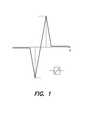
- FIG. 1shows the schematic I-V curve, including all quadrants, for the ideal secondary surge protector operation.
- transient blocking unitswere proposed to achieve characteristic performance shown in FIG. 1 .
- a variety of such transient blocking unitshave been published as U.S. published applications 20080192394, 20060285264, 20060176638, 20060098373, 20060098364, and 20060098363, all of which are hereby incorporated by reference.
- FIG. 2shows such a prior art device made from two MOSFETs as shown (G 1 , D 1 and G 2 , D 2 respectively). Notice that, to operate at small voltages, each MOSFET should possess a small threshold voltage, and therefore a small gate oxide thickness at G 1 and G 2 . In practice, in embodiments designed for handling significant voltage, one cannot apply full drain voltage to the low threshold gate, because the thin gate oxide may be damaged and the device may be destroyed. Therefore, additional circuit elements had to be added in order to overcome the above problems.
- the present applicationdiscloses new approaches to an electronic device, referred to hereinafter as a series current limiter (SCL) device, which uses a Regenerative building block (RBB), such as disclosed in U.S. patent application Ser. No. 12/359,094 filed Jan. 23, 2009, which is hereby incorporated by reference.
- SCLseries current limiter
- RBMRegenerative building block
- the present inventorshave realized that the self-bootstrapping diode described in commonly owned U.S. patent application Ser. No. 12/683,425 provides a very good “lambda device” characteristic in its reverse-bias regime, and that the limiting current density of this reverse-bias regime can be easily adjusted.
- the present inventorshave also realized that, by combining two such devices with opposing polarities, a transient blocking device can be achieved which provides bidirectional lambda device characteristics. Many different embodiments are described.
- FIG. 1shows a schematic I-V curve for an ideal secondary surge protector operation.
- FIG. 2shows an example of a conventional series current limiting (or transient blocking) device made from two MOSFETs.
- FIG. 3shows a schematic for a Series Current Limiter made from two Regenerative Building Blocks.
- FIG. 4shows a Series Current Limiter made from the combination of a P-channel and a N-channel Regenerative Building Block.
- the probe electrode of either RBBis connected to the gate electrode of the other, and this configuration provides automatic switching between ON and OFF states.
- FIG. 5shows a schematic for a Series Current Limiter made from the combination of a Regenerative Building Block and a MOSFET.
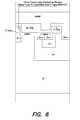
- FIG. 6is a structural representation of a Series Current Limiter made from the combination of a N-type Regenerative Building Block and a P-type MOSFET.
- FIG. 7is a graph showing the reverse bias with forward voltage drop versus applied current for a Series Current Limiter device, both at 125 C (the upper line) and at 25 C (the lower line).
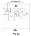
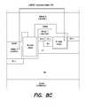
- FIGS. 8A , 8 B, 8 C, and 8 Dshow four different UMOS realizations of Series Current Limiter devices.
- the present applicationdiscloses new approaches to an electronic device, referred to hereinafter as a series current limiter (SCL) device, which uses a Regenerative building block (RBB), such as disclosed in U.S. patent application Ser. No. 12/359,094 filed Jan. 23, 2009, which is hereby incorporated by reference.
- SCLseries current limiter
- RBMRegenerative building block
- the present inventorshave realized that the self-bootstrapping diode described in commonly owned U.S. patent application Ser. No. 12/683,425 provides a very good “lambda device” characteristic in its reverse-bias regime, and that the limiting current density can be easily adjusted.
- the present inventorshave also realized that, by combining two such devices with opposing polarities, a transient blocking device can be achieved which provides bidirectional lambda device characteristics. Many different embodiments are described.
- the deviceuses two external electrodes to achieve a voltage-current characteristic very close to the ideal one shown on FIG. 1 .
- the use of such an Regenerative Building Blockavoids the problems of a large gate signal which can occur in the known structure of FIG. 2 .
- the Series Current Limiter devicecan be built as a regenerative combination of a Regenerative Building Block (RBB) together with another Regenerative Building Block or MOSFET: one of a P-type and the other of the N-type ( FIG. 3 and FIG. 5 ) with both channels normally in the conductive ON state.
- RBBRegenerative Building Block
- MOSFETRegenerative Building Block
- the regenerative configurationproduces the effect that both channels stay in the conductive ON state for increasing applied voltage until one of the regenerative signals reaches the threshold voltage. After that occurs, both regenerative couplings turn both channels into blocking OFF state.
- FIGS. 3 and 5provide only unidirectional protection, since for the forward bias they act as small resistors. Two such devices connected back-to-back in series will provide bidirectional protection as shown for the ideal device of FIG. 1 . Since the series current limiter device has only two contacts and is used for both incoming lines, the complexity of coordination between primary and secondary surge protection is avoided. The use of a voltage probe electrode automatically restricts the maximum voltage on the gate, providing gate protection.
- the device parameterscan be adjusted so that it is more difficult to switch the active device to its OFF state.
- the “bootstrap” diode of Ser. No. 12/683,425was modified by doubling the gate oxide thickness (from 50 ⁇ to 100 ⁇ ), and by reducing the channel doping by a factor of 6 (changing from an implant of 6 ⁇ 10 12 cm ⁇ 2 boron at 30 keV to an implant of 1 ⁇ 10 12 cm ⁇ 2 boron at 30 keV).
- these specific numbersare merely examples of how a particular process was modified, but they do help to show an example of what sort of changes can be useful to optimize the device for use as a transient blocking unit.
- optimization of the bootstrap diode structure for use as a transient blocking unitshould make the diode leaky.
- the maximum peak current through a diode optimized for transient blockingis preferably several orders of magnitudes larger than that of the same structure optimized for fast reaction and low forward voltage drop.
- the present applicationdiscloses a new series current limiter (SCL) device, which (in one example) can be viewed in simplified form, as a regenerative combination of two MOSFETs, where one of the MOSFETs has an extra voltage probe electrode that provides a regenerative signal with self-limited voltage that cannot destroy the other gate.
- SCLseries current limiter
- FIG. 3A generalized schematic representation of the internal configuration of one embodiment of Series Current Limiter, comprising a combination of a specially-constructed N-type Regenerative Building Block 310 and a specially-constructed P-type Regenerative Building Block 320 , is shown in FIG. 3 .
- the source electrodes S of the two Regenerative Building Blocks ( 301 and 302 )are shorted together.
- the gate electrode of each Regenerative Building Block, indicated as G 1 312 and G 2 322is controlled by a regenerative signal from the probe contact P 2 323 (and P 1 313 ) of the other Regenerative Building Block.
- the drain electrode D 2 324 of the N-type Regenerative Building Block G 2 322serves as a cathode K for the Series Current Limiter, and the drain electrode D 1 314 of the P-type Regenerative Building Block as an anode A.
- the cathode and anodeare the only external electrodes.
- both P and N channelsare open and the device has small resistance.
- the probe electrode of the Regenerative Building Blockprovides a low voltage well defined regenerative signal, which is well-suited for the gate electrode of the adjacent device.
- the regenerative voltages above the thresholdwill close both of the channels.
- the deviceoperates as a unidirectional protection device, and can be represented by the symbol shown in FIG. 1 , which reflects the ideal protector characteristic.
- the thickness of the gate oxide and the doping in the channel regionare carefully managed to optimize device performance.
- N++doping in the probe openingis preferred over P++doping in at least some embodiments.
- FIG. 4shows the configuration for one side of a Series Current Limiter, using the combination of a P-channel and an N-channel Regenerative Building Block. Using modifications as described above, the maximum current density of the reverse-biased device can be made usefully large. By using a series combination of two such devices back-to-back, a bidirectional Transient Blocking Unit can be achieved.
- one side of a Series Current Limitercan be also made from a combination of a Regenerative Building Block and a MOSFET.
- FIG. 5shows an embodiment of such a device in schematic form
- FIG. 6illustrates the structure of such an embodiment of a Series Current Limiter in accordance with a sample innovative embodiment.
- the maximum current density of the reverse-biased devicecan be made usefully large.
- a bidirectional Transient Blocking Unitcan be achieved.
- the IV curve for reverse biasis shown in FIG. 7 .
- the Series Current Limiter performance in accordance with the inventionsresembles the ideal case.
- the peak current density at 0.2Vis 30 A/cm 2 , which is appropriate to make the protection device.
- the areais 0.01 cm 2 and series resistance is only 0.67 ohm.
- FIGS. 8A-8Dillustrate further alternatives of one side of a Series Current Limiter device, using UMOS technology for fabricating the Series Current Limiter device.
- the reverse-biased device characteristicscan be optimized for a Transient Blocking Unit.
- a bidirectional Transient Blocking Unitcan be achieved.
- a transient current blocking unitcomprising: a pair of self-bootstrapping diodes connected together in series with opposed polarities; wherein each said diode is optimized for a maximum current density, under reverse bias, which is more than ten times the maximum current density which would occur in said diode if optimized for rectification.
- a transient current blocking unitcomprising: a pair of diodes connected together in series with opposed polarities; at least one of said diodes comprising a semiconductor device which includes: a first semiconductor channel which electrically separates a first semiconductor source of a first conductivity type from a first drift region, and which is gated by a first gate electrode; a second semiconductor channel which electrically separates a second semiconductor source of a second conductivity type from a second drift region, and which is gated by a second gate electrode; said first and second sources being electrically connected together; a first external terminal, which is operatively connected to receive first-type majority carriers through said first drift region, and a second external terminal, which is operatively connected to receive second-type majority carriers through said second drift region; said first gate electrode being operatively connected to receive a potential which is dependent on the potential of said second drift region, and said second gate electrode being operatively connected to receive a potential which is dependent on the potential of said first drift region; wherein each
- a method for limiting transient current between two terminalscomprising the actions of: connecting a pair of diodes in series between said terminals, said diodes being connected with opposed polarities; and when a cathode terminal of either said diode is more negative than an anode terminal thereof, then sinking current from said anode terminal through a first drift region and a first field-effect-gated channel to an n-type source, and also sourcing current to said cathode terminal from a p-type source through a second field-effect-gated channel and a second drift region; said n-type and p-type sources being electrically connected together; said second channel being gated by a second gate electrode which is coupled to said first drift region; and said first channel being gated by a first gate electrode which is coupled to said second drift region; wherein each said diode is optimized for a maximum current density, under reverse bias, which is more than ten times the maximum current density which would occur in said diode
Landscapes
- Semiconductor Integrated Circuits (AREA)
- Metal-Oxide And Bipolar Metal-Oxide Semiconductor Integrated Circuits (AREA)
- Emergency Protection Circuit Devices (AREA)
Abstract
Description
- Greater robustness and reliability.
- Greater operatively across a wider voltage range.
- One device can be utilized for current limiting rather than multiple devices as previously required.
Claims (55)
Priority Applications (1)
| Application Number | Priority Date | Filing Date | Title |
|---|---|---|---|
| US12/773,003US8643055B2 (en) | 2007-09-26 | 2010-05-03 | Series current limiter device |
Applications Claiming Priority (10)
| Application Number | Priority Date | Filing Date | Title |
|---|---|---|---|
| US97546707P | 2007-09-26 | 2007-09-26 | |
| US2296808P | 2008-01-23 | 2008-01-23 | |
| US4833608P | 2008-04-28 | 2008-04-28 | |
| US12/238,308US8148748B2 (en) | 2007-09-26 | 2008-09-25 | Adjustable field effect rectifier |
| US14264709P | 2009-01-06 | 2009-01-06 | |
| US12/359,094US8421118B2 (en) | 2007-09-26 | 2009-01-23 | Regenerative building block and diode bridge rectifier and methods |
| US12/431,580US8598620B2 (en) | 2007-09-26 | 2009-04-28 | MOSFET with integrated field effect rectifier |
| US17486509P | 2009-05-01 | 2009-05-01 | |
| US12/683,425US8633521B2 (en) | 2007-09-26 | 2010-01-06 | Self-bootstrapping field effect diode structures and methods |
| US12/773,003US8643055B2 (en) | 2007-09-26 | 2010-05-03 | Series current limiter device |
Related Parent Applications (1)
| Application Number | Title | Priority Date | Filing Date |
|---|---|---|---|
| US12/683,425ContinuationUS8633521B2 (en) | 2007-09-26 | 2010-01-06 | Self-bootstrapping field effect diode structures and methods |
Publications (2)
| Publication Number | Publication Date |
|---|---|
| US20110051305A1 US20110051305A1 (en) | 2011-03-03 |
| US8643055B2true US8643055B2 (en) | 2014-02-04 |
Family
ID=43032823
Family Applications (1)
| Application Number | Title | Priority Date | Filing Date |
|---|---|---|---|
| US12/773,003Expired - Fee RelatedUS8643055B2 (en) | 2007-09-26 | 2010-05-03 | Series current limiter device |
Country Status (2)
| Country | Link |
|---|---|
| US (1) | US8643055B2 (en) |
| WO (1) | WO2010127370A2 (en) |
Cited By (4)
| Publication number | Priority date | Publication date | Assignee | Title |
|---|---|---|---|---|
| US20140319577A1 (en)* | 2013-04-24 | 2014-10-30 | Denso Corporation | Semiconductor device |
| US9029921B2 (en)* | 2007-09-26 | 2015-05-12 | Stmicroelectronics International N.V. | Self-bootstrapping field effect diode structures and methods |
| US10205313B2 (en) | 2015-07-24 | 2019-02-12 | Symptote Technologies, LLC | Two-transistor devices for protecting circuits from sustained overcurrent |
| US10770883B2 (en) | 2015-09-21 | 2020-09-08 | Sympote Technologies LLC | One-transistor devices for protecting circuits and autocatalytic voltage conversion therefor |
Families Citing this family (3)
| Publication number | Priority date | Publication date | Assignee | Title |
|---|---|---|---|---|
| US9018048B2 (en) | 2012-09-27 | 2015-04-28 | Stmicroelectronics S.R.L. | Process for manufactuirng super-barrier rectifiers |
| FR3012699A1 (en)* | 2013-10-31 | 2015-05-01 | St Microelectronics Tours Sas | CONTROL CIRCUIT FOR DIODES IN HALF-BRIDGE |
| EP3261129B1 (en)* | 2016-04-15 | 2020-05-06 | STMicroelectronics (Tours) SAS | Diode structure |
Citations (137)
| Publication number | Priority date | Publication date | Assignee | Title |
|---|---|---|---|---|
| US3602777A (en) | 1970-04-21 | 1971-08-31 | Westinghouse Electric Corp | Silicon carbide semiconductor device with heavily doped silicon carbide ohmic contacts |
| US3603811A (en) | 1969-12-09 | 1971-09-07 | American Optical Corp | Two-terminal bipolar self-powered low current limiter |
| US4281448A (en) | 1980-04-14 | 1981-08-04 | Gte Laboratories Incorporated | Method of fabricating a diode bridge rectifier in monolithic integrated circuit structure utilizing isolation diffusions and metal semiconductor rectifying barrier diode formation |
| US4373252A (en) | 1981-02-17 | 1983-02-15 | Fairchild Camera & Instrument | Method for manufacturing a semiconductor structure having reduced lateral spacing between buried regions |
| US4533970A (en) | 1983-06-27 | 1985-08-06 | Motorola, Inc. | Series current limiter |
| US4599576A (en) | 1977-04-15 | 1986-07-08 | Hitachi, Ltd. | Insulated gate type field effect semiconductor device and a circuit employing the device |
| US4610730A (en) | 1984-12-20 | 1986-09-09 | Trw Inc. | Fabrication process for bipolar devices |
| US4630084A (en) | 1981-02-02 | 1986-12-16 | Siemens Aktiengesellschaft | Vertical mis-field effect transistor with low forward resistance |
| US4722856A (en) | 1986-01-02 | 1988-02-02 | Molecular Electronics Corporation | Method and apparatus for depositing monomolecular layers on a substrate |
| US4843441A (en) | 1987-08-10 | 1989-06-27 | Willard Jerry W | High frequency, high power field effect transistor |
| EP0322400A2 (en) | 1984-10-03 | 1989-06-28 | Giroflex-Entwicklungs AG | Chair frame with a reclining seat and a backrest support |
| US4903189A (en) | 1988-04-27 | 1990-02-20 | General Electric Company | Low noise, high frequency synchronous rectifier |
| US4955069A (en) | 1989-03-02 | 1990-09-04 | Ionescu Adrian F | A.C. power controller with short circuit and overload protection |
| US4962411A (en) | 1986-03-21 | 1990-10-09 | Nippondenso Co., Ltd. | Semiconductor device with current detecting function |
| US4967243A (en) | 1988-07-19 | 1990-10-30 | General Electric Company | Power transistor structure with high speed integral antiparallel Schottky diode |
| US4969028A (en) | 1980-12-02 | 1990-11-06 | General Electric Company | Gate enhanced rectifier |
| US4980741A (en) | 1989-02-10 | 1990-12-25 | General Electric Company | MOS protection device |
| US4982260A (en) | 1989-10-02 | 1991-01-01 | General Electric Company | Power rectifier with trenches |
| US4996581A (en) | 1988-02-03 | 1991-02-26 | Kabushiki Kaisha Toshiba | Bipolar transistor |
| US5019530A (en) | 1990-04-20 | 1991-05-28 | International Business Machines Corporation | Method of making metal-insulator-metal junction structures with adjustable barrier heights |
| US5021861A (en) | 1990-05-23 | 1991-06-04 | North Carolina State University | Integrated circuit power device with automatic removal of defective devices and method of fabricating same |
| US5070377A (en) | 1990-02-15 | 1991-12-03 | Mitsubishi Denki Kabushiki Kaisha | Semiconductor device and method of manufacturing the same |
| US5111253A (en) | 1989-05-09 | 1992-05-05 | General Electric Company | Multicellular FET having a Schottky diode merged therewith |
| US5304831A (en) | 1990-12-21 | 1994-04-19 | Siliconix Incorporated | Low on-resistance power MOS technology |
| US5381025A (en) | 1989-08-17 | 1995-01-10 | Ixys Corporation | Insulated gate thyristor with gate turn on and turn off |
| US5387805A (en) | 1994-01-05 | 1995-02-07 | Metzler; Richard A. | Field controlled thyristor |
| US5396085A (en) | 1993-12-28 | 1995-03-07 | North Carolina State University | Silicon carbide switching device with rectifying-gate |
| US5410171A (en) | 1992-03-30 | 1995-04-25 | Nippondenso Co., Ltd. | Vertical type semiconductor with main current section and emulation current section |
| US5416354A (en) | 1989-01-06 | 1995-05-16 | Unitrode Corporation | Inverted epitaxial process semiconductor devices |
| US5430315A (en) | 1993-07-22 | 1995-07-04 | Rumennik; Vladimir | Bi-directional power trench MOS field effect transistor having low on-state resistance and low leakage current |
| US5446295A (en) | 1993-08-23 | 1995-08-29 | Siemens Components, Inc. | Silicon controlled rectifier with a variable base-shunt resistant |
| US5532502A (en) | 1991-10-24 | 1996-07-02 | Fuji Electric Co., Ltd. | Conductivity-modulated-type MOSFET |
| US5545573A (en) | 1994-06-01 | 1996-08-13 | Mitsubishi Denki Kabushiki Kaisha | Method of fabricating insulated gate semiconductor device |
| US5554880A (en) | 1994-08-08 | 1996-09-10 | Semicoa Semiconductors | Uniform current density and high current gain bipolar transistor |
| US5559355A (en) | 1994-03-04 | 1996-09-24 | Fuji Electric Co., Ltd. | Vertical MOS semiconductor device |
| US5621234A (en) | 1991-10-07 | 1997-04-15 | Niipondenso Co., Ltd. | Vertical semiconductor device with breakdown voltage improvement region |
| US5629536A (en) | 1995-11-21 | 1997-05-13 | Motorola, Inc. | High voltage current limiter and method for making |
| US5643809A (en) | 1995-03-08 | 1997-07-01 | Integrated Device Technology, Inc. | Method for making high speed poly-emitter bipolar transistor |
| EP0807979A2 (en) | 1996-05-15 | 1997-11-19 | SILICONIX Incorporated | Diode |
| US5719411A (en) | 1994-07-28 | 1998-02-17 | International Rectifier Corporation | Three-terminal MOS-gate controlled thyristor structures with current saturation characteristics |
| US5742463A (en) | 1993-07-01 | 1998-04-21 | The University Of Queensland | Protection device using field effect transistors |
| US5744994A (en) | 1996-05-15 | 1998-04-28 | Siliconix Incorporated | Three-terminal power mosfet switch for use as synchronous rectifier or voltage clamp |
| US5747841A (en) | 1994-12-20 | 1998-05-05 | U.S. Philips Corporation | Circuit arrangement, and junction field effect transistor suitable for use in such a circuit arrangement |
| US5825079A (en) | 1997-01-23 | 1998-10-20 | Luminous Intent, Inc. | Semiconductor diodes having low forward conduction voltage drop and low reverse current leakage |
| US5869380A (en) | 1998-07-06 | 1999-02-09 | Industrial Technology Research Institute | Method for forming a bipolar junction transistor |
| US5877515A (en) | 1995-10-10 | 1999-03-02 | International Rectifier Corporation | SiC semiconductor device |
| US5886383A (en) | 1997-01-10 | 1999-03-23 | International Rectifier Corporation | Integrated schottky diode and mosgated device |
| US5898982A (en) | 1997-05-30 | 1999-05-04 | Luminous Intent, Inc. | Thin film capacitors |
| US5932922A (en) | 1994-08-08 | 1999-08-03 | Semicoa Semiconductors | Uniform current density and high current gain bipolar transistor |
| US5956582A (en) | 1993-05-10 | 1999-09-21 | Sgs-Thomson Microelectronics S.A. | Current limiting circuit with continuous metallization |
| US6034385A (en) | 1995-12-22 | 2000-03-07 | Siemens Aktiengesellschaft | Current-limiting semiconductor configuration |
| US6048788A (en) | 1997-11-24 | 2000-04-11 | United Microelectronics Corp. | Method of fabricating metal plug |
| US6051850A (en) | 1995-12-30 | 2000-04-18 | Fairchild Korea Semiconductor Ltd. | Insulated gate bipolar junction transistors having built-in freewheeling diodes therein |
| US6078074A (en) | 1996-12-06 | 2000-06-20 | Kabushiki Kaisha Toshiba | Semiconductor device having multilayer metal interconnection |
| US6097046A (en) | 1993-04-30 | 2000-08-01 | Texas Instruments Incorporated | Vertical field effect transistor and diode |
| US6100145A (en) | 1998-11-05 | 2000-08-08 | Advanced Micro Devices, Inc. | Silicidation with silicon buffer layer and silicon spacers |
| US6169300B1 (en) | 1997-03-11 | 2001-01-02 | Sgs-Thomson Microelectronics S.R.L. | Insulated gate bipolar transistor with high dynamic ruggedness |
| US6172398B1 (en) | 1997-08-11 | 2001-01-09 | Magepower Semiconductor Corp. | Trenched DMOS device provided with body-dopant redistribution-compensation region for preventing punch through and adjusting threshold voltage |
| US6186408B1 (en) | 1999-05-28 | 2001-02-13 | Advanced Power Devices, Inc. | High cell density power rectifier |
| US6225280B1 (en) | 1995-11-09 | 2001-05-01 | Akzo-Pq Silica Vof | Compacted sodium silicate |
| US6235601B1 (en) | 1995-12-28 | 2001-05-22 | Philips Electronics North America Corporation | Method of manufacturing a self-aligned vertical bipolar transistor |
| US6242324B1 (en) | 1999-08-10 | 2001-06-05 | The United States Of America As Represented By The Secretary Of The Navy | Method for fabricating singe crystal materials over CMOS devices |
| US6258634B1 (en) | 1998-06-19 | 2001-07-10 | National Semiconductor Corporation | Method for manufacturing a dual-direction over-voltage and over-current IC protection device and its cell structure |
| US6268758B1 (en) | 1999-04-16 | 2001-07-31 | Patent-Treuhand-Gesellschaft Fuer Elektrische Gluehlampen Mbh | Circuit arrangement with half-bridge |
| US6281547B1 (en) | 1997-05-08 | 2001-08-28 | Megamos Corporation | Power transistor cells provided with reliable trenched source contacts connected to narrower source manufactured without a source mask |
| US6313001B1 (en) | 1998-11-04 | 2001-11-06 | Telefonaktiebolaget Lm Ericsson (Publ) | Method for semiconductor manufacturing |
| US6323091B1 (en) | 1999-07-16 | 2001-11-27 | Zilog, Inc. | Method of forming semiconductor memory device with LDD |
| US20010045635A1 (en)* | 2000-02-10 | 2001-11-29 | International Rectifier Corp. | Vertical conduction flip-chip device with bump contacts on single surface |
| US6331455B1 (en) | 1999-04-01 | 2001-12-18 | Advanced Power Devices, Inc. | Power rectifier device and method of fabricating power rectifier devices |
| US20020024375A1 (en) | 2000-05-15 | 2002-02-28 | Tetsuro Asano | Compound semiconductor switching device for high frequency switching |
| US6362036B1 (en) | 1998-02-10 | 2002-03-26 | Stmicroelectronics S.R.L. | VDMOS transistor protected against over-voltages between source and gate |
| US6373097B1 (en) | 1996-09-19 | 2002-04-16 | Infineon Technologies Ag | Field-effect-controllable, vertical semiconductor component, and monolithically integrated half bridge |
| US6384456B1 (en) | 1997-09-30 | 2002-05-07 | Infineon Technologies Ag | Field-effect transistor having a high packing density and method for fabricating it |
| US6392859B1 (en)* | 1999-02-14 | 2002-05-21 | Yazaki Corporation | Semiconductor active fuse for AC power line and bidirectional switching device for the fuse |
| US6399996B1 (en) | 1999-04-01 | 2002-06-04 | Apd Semiconductor, Inc. | Schottky diode having increased active surface area and method of fabrication |
| US6404033B1 (en) | 1999-04-01 | 2002-06-11 | Apd Semiconductor, Inc. | Schottky diode having increased active surface area with improved reverse bias characteristics and method of fabrication |
| US6420225B1 (en) | 1999-04-01 | 2002-07-16 | Apd Semiconductor, Inc. | Method of fabricating power rectifier device |
| US6426541B2 (en) | 2000-07-20 | 2002-07-30 | Apd Semiconductor, Inc. | Schottky diode having increased forward current with improved reverse bias characteristics and method of fabrication |
| US6448160B1 (en) | 1999-04-01 | 2002-09-10 | Apd Semiconductor, Inc. | Method of fabricating power rectifier device to vary operating parameters and resulting device |
| US6459108B1 (en) | 1997-04-25 | 2002-10-01 | Siemens Aktiengesellschaft | Semiconductor configuration and current limiting device |
| US20020177324A1 (en) | 2001-05-23 | 2002-11-28 | Metzler Richard A. | Vertical metal oxide silicon field effect semiconductor diodes |
| US20020179968A1 (en)* | 2001-05-30 | 2002-12-05 | Frank Pfirsch | Power semiconductor component, compensation component, power transistor, and method for producing power semiconductor components |
| US6498367B1 (en) | 1999-04-01 | 2002-12-24 | Apd Semiconductor, Inc. | Discrete integrated circuit rectifier device |
| US6515330B1 (en) | 2002-01-02 | 2003-02-04 | Apd Semiconductor, Inc. | Power device having vertical current path with enhanced pinch-off for current limiting |
| US20030025152A1 (en) | 2001-06-19 | 2003-02-06 | Wolfgang Werner | Field-effect controlled semiconductor component and method of manufacturing a field-effect controlled semiconductor component |
| US6537860B2 (en) | 2000-12-18 | 2003-03-25 | Apd Semiconductor, Inc. | Method of fabricating power VLSI diode devices |
| US20030146474A1 (en) | 2002-02-05 | 2003-08-07 | Industrial Technology Research Institute | SCR devices in silicon-on-insulator CMOS process for on-chip ESD protection |
| US6624030B2 (en) | 2000-12-19 | 2003-09-23 | Advanced Power Devices, Inc. | Method of fabricating power rectifier device having a laterally graded P-N junction for a channel region |
| US6630698B1 (en) | 1998-09-02 | 2003-10-07 | Infineon Ag | High-voltage semiconductor component |
| US20030207538A1 (en) | 2000-10-06 | 2003-11-06 | Fwu-Iuan Hshieh | Trench DMOS transistor with embedded trench schottky rectifier |
| US20030222290A1 (en) | 2002-05-30 | 2003-12-04 | Apd Semiconductor, Inc. | Power device having reduced reverse bias leakage current |
| US20040041619A1 (en) | 2002-06-06 | 2004-03-04 | International Recitifier Corporation | Mosgate driver integrated circuit with adaptive dead time |
| US6724039B1 (en) | 1998-08-31 | 2004-04-20 | Stmicroelectronics, Inc. | Semiconductor device having a Schottky diode |
| US6784489B1 (en) | 1997-03-28 | 2004-08-31 | Stmicroelectronics, Inc. | Method of operating a vertical DMOS transistor with schottky diode body structure |
| US6828605B2 (en) | 2000-12-11 | 2004-12-07 | Infineon Technologies Ag | Field-effect-controlled semiconductor component and method of fabricating a doping layer in a vertically configured semiconductor component |
| US6853036B1 (en) | 2003-08-06 | 2005-02-08 | Esd Pulse, Inc. | Method and apparatus for preventing microcircuit dynamic thermo-mechanical damage during an ESD event |
| US20050029585A1 (en) | 2003-08-04 | 2005-02-10 | Donald He | Integrated fet and schottky device |
| US20050116313A1 (en) | 2003-11-28 | 2005-06-02 | Lee Jae-Gil | Superjunction semiconductor device |
| US20050152080A1 (en) | 2003-08-21 | 2005-07-14 | Fultec Semiconductor Inc. | Integrated electronic disconnecting circuits, methods, and systems |
| US20050189658A1 (en) | 2004-01-29 | 2005-09-01 | Tan Xiaochun | Semiconductor device assembly process |
| US20050189626A1 (en) | 2004-01-29 | 2005-09-01 | Tan Xiaochun | Semiconductor device support structures |
| US20050200394A1 (en) | 2004-03-10 | 2005-09-15 | Brad Underwood | Systems and methods for providing distributed control signal redundancy among electronic circuits |
| US6956266B1 (en) | 2004-09-09 | 2005-10-18 | International Business Machines Corporation | Structure and method for latchup suppression utilizing trench and masked sub-collector implantation |
| US20050231355A1 (en) | 2003-06-26 | 2005-10-20 | Abet Technologies, Llc | Method and system for bidirectional data and power transmission |
| US20050243496A1 (en) | 2002-10-08 | 2005-11-03 | Fultec Pty. Ltd. | Protection devices and methods for preventing the flow of undesirable differential mode transients |
| US6967374B1 (en) | 2004-07-07 | 2005-11-22 | Kabushiki Kaisha Toshiba | Power semiconductor device |
| US6992353B1 (en) | 2004-11-01 | 2006-01-31 | Silicon-Based Technology Corp. | Self-aligned source structure of planar DMOS power transistor and its manufacturing methods |
| US7009253B2 (en) | 2003-08-06 | 2006-03-07 | Esd Pulse, Inc. | Method and apparatus for preventing microcircuit thermo-mechanical damage during an ESD event |
| US20060071295A1 (en)* | 2004-09-27 | 2006-04-06 | Rockwell Scientific Licensing, Llc. | High voltage FET switch with conductivity modulation |
| US20060098364A1 (en) | 2004-11-09 | 2006-05-11 | Fultec Semiconductor, Inc. | Apparatus and method for enhanced transient blocking |
| US20060098373A1 (en) | 2004-11-09 | 2006-05-11 | Fultec Semiconductors, Inc. | Intelligent transient blocking unit |
| US20060098363A1 (en) | 2004-11-09 | 2006-05-11 | Fultec Semiconductors, Inc. | Integrated transient blocking unit compatible with very high voltages |
| US20060145260A1 (en) | 2004-12-30 | 2006-07-06 | Magnachip Semiconductor Ltd. | Electro-static discharge protection circuit and method for fabricating the same |
| US20060158812A1 (en) | 2005-01-14 | 2006-07-20 | Harris Richard A | Transient blocking unit having shunt for over-voltage protection |
| US20060158816A1 (en) | 2005-01-14 | 2006-07-20 | Harris Richard A | Low resistance transient blocking unit |
| US7087981B2 (en) | 2002-04-19 | 2006-08-08 | Infineon Technologies Ag | Metal semiconductor contact, semiconductor component, integrated circuit arrangement and method |
| US20060176638A1 (en) | 2005-02-10 | 2006-08-10 | Fultec Semiconductors, Inc. | Minimized wire bonds in transient blocking unit packaging |
| US7095113B2 (en) | 2004-01-29 | 2006-08-22 | Diodes Incorporated | Semiconductor device with interlocking clip |
| US20060250736A1 (en) | 2005-05-06 | 2006-11-09 | Harris Richard A | Transient blocking apparatus with electrostatic discharge protection |
| US20060285264A1 (en) | 2005-06-16 | 2006-12-21 | Fultec Semiconductor, Inc. | Transient blocking apparatus with reset |
| US7220319B2 (en)* | 2002-04-16 | 2007-05-22 | Canon Anelva Corporation | Electrostatic chucking stage and substrate processing apparatus |
| US7250668B2 (en) | 2005-01-20 | 2007-07-31 | Diodes, Inc. | Integrated circuit including power diode |
| US20070235752A1 (en) | 2006-03-24 | 2007-10-11 | Fujifilm Corporation | Insulated gate type thyristor |
| US20080017930A1 (en) | 2005-02-22 | 2008-01-24 | Samsung Electronics Co., Ltd. | Dual work function metal gate structure and related method of manufacture |
| US7342389B1 (en) | 2007-01-09 | 2008-03-11 | Diodes, Inc. | High efficiency charge pump DC to DC converter circuits and methods |
| US20080079035A1 (en) | 2006-09-30 | 2008-04-03 | Alpha & Omega Semiconductor, Ltd. | Symmetric blocking transient voltage suppressor (TVS) using bipolar transistor base snatch |
| US20080079065A1 (en)* | 2006-09-29 | 2008-04-03 | Qingchun Zhang | Novel U-Shape Metal-Oxide-Semiconductor (UMOS) Gate Structure For High Power MOS-Based Semiconductor Devices |
| USRE40222E1 (en) | 1999-01-25 | 2008-04-08 | Stmicroelectronics S.R.L. | Electronic semiconductor power device with integrated diode |
| US20080137249A1 (en) | 2006-10-27 | 2008-06-12 | Harris Richard A | Mitigation of current collapse in transient blocking units |
| US20080192394A1 (en) | 2004-11-12 | 2008-08-14 | Harris Richard A | Surge Protection Device |
| US20080265975A1 (en) | 2007-04-25 | 2008-10-30 | Denso Corporation | Method for controlling vertical type MOSFET in bridge circuit |
| US20080284383A1 (en)* | 2007-05-14 | 2008-11-20 | Atmel Corporation | Charge Detector |
| US20090026492A1 (en) | 2007-07-25 | 2009-01-29 | Chatty Kiran V | Lateral junction breakdown triggered silicon controlled rectifier based electrostatic discharge protection device |
| US7781826B2 (en) | 2006-11-16 | 2010-08-24 | Alpha & Omega Semiconductor, Ltd. | Circuit configuration and manufacturing processes for vertical transient voltage suppressor (TVS) and EMI filter |
| US20100271851A1 (en)* | 2007-09-26 | 2010-10-28 | Lakota Technologies Inc. | Self-bootstrapping field effect diode structures and methods |
| US7893489B2 (en) | 2007-04-26 | 2011-02-22 | Renesas Electronics Corporation | Semiconductor device having vertical MOSFET |
| US8148748B2 (en)* | 2007-09-26 | 2012-04-03 | Stmicroelectronics N.V. | Adjustable field effect rectifier |
- 2010
- 2010-05-03USUS12/773,003patent/US8643055B2/ennot_activeExpired - Fee Related
- 2010-05-03WOPCT/US2010/033451patent/WO2010127370A2/enactiveApplication Filing
Patent Citations (155)
| Publication number | Priority date | Publication date | Assignee | Title |
|---|---|---|---|---|
| US3603811A (en) | 1969-12-09 | 1971-09-07 | American Optical Corp | Two-terminal bipolar self-powered low current limiter |
| US3602777A (en) | 1970-04-21 | 1971-08-31 | Westinghouse Electric Corp | Silicon carbide semiconductor device with heavily doped silicon carbide ohmic contacts |
| US4599576A (en) | 1977-04-15 | 1986-07-08 | Hitachi, Ltd. | Insulated gate type field effect semiconductor device and a circuit employing the device |
| US4281448A (en) | 1980-04-14 | 1981-08-04 | Gte Laboratories Incorporated | Method of fabricating a diode bridge rectifier in monolithic integrated circuit structure utilizing isolation diffusions and metal semiconductor rectifying barrier diode formation |
| US4969028A (en) | 1980-12-02 | 1990-11-06 | General Electric Company | Gate enhanced rectifier |
| US4630084A (en) | 1981-02-02 | 1986-12-16 | Siemens Aktiengesellschaft | Vertical mis-field effect transistor with low forward resistance |
| US4373252A (en) | 1981-02-17 | 1983-02-15 | Fairchild Camera & Instrument | Method for manufacturing a semiconductor structure having reduced lateral spacing between buried regions |
| US4533970A (en) | 1983-06-27 | 1985-08-06 | Motorola, Inc. | Series current limiter |
| EP0322400A2 (en) | 1984-10-03 | 1989-06-28 | Giroflex-Entwicklungs AG | Chair frame with a reclining seat and a backrest support |
| US4610730A (en) | 1984-12-20 | 1986-09-09 | Trw Inc. | Fabrication process for bipolar devices |
| US4722856A (en) | 1986-01-02 | 1988-02-02 | Molecular Electronics Corporation | Method and apparatus for depositing monomolecular layers on a substrate |
| US4783348A (en) | 1986-01-02 | 1988-11-08 | Daleco Research Development | Method and apparatus for depositing monomolecular layers on a substrate |
| US4962411A (en) | 1986-03-21 | 1990-10-09 | Nippondenso Co., Ltd. | Semiconductor device with current detecting function |
| US4843441A (en) | 1987-08-10 | 1989-06-27 | Willard Jerry W | High frequency, high power field effect transistor |
| US4996581A (en) | 1988-02-03 | 1991-02-26 | Kabushiki Kaisha Toshiba | Bipolar transistor |
| US4903189A (en) | 1988-04-27 | 1990-02-20 | General Electric Company | Low noise, high frequency synchronous rectifier |
| US4967243A (en) | 1988-07-19 | 1990-10-30 | General Electric Company | Power transistor structure with high speed integral antiparallel Schottky diode |
| US5416354A (en) | 1989-01-06 | 1995-05-16 | Unitrode Corporation | Inverted epitaxial process semiconductor devices |
| US4980741A (en) | 1989-02-10 | 1990-12-25 | General Electric Company | MOS protection device |
| US4955069A (en) | 1989-03-02 | 1990-09-04 | Ionescu Adrian F | A.C. power controller with short circuit and overload protection |
| US5111253A (en) | 1989-05-09 | 1992-05-05 | General Electric Company | Multicellular FET having a Schottky diode merged therewith |
| US5381025A (en) | 1989-08-17 | 1995-01-10 | Ixys Corporation | Insulated gate thyristor with gate turn on and turn off |
| US4982260A (en) | 1989-10-02 | 1991-01-01 | General Electric Company | Power rectifier with trenches |
| US5070377A (en) | 1990-02-15 | 1991-12-03 | Mitsubishi Denki Kabushiki Kaisha | Semiconductor device and method of manufacturing the same |
| US5019530A (en) | 1990-04-20 | 1991-05-28 | International Business Machines Corporation | Method of making metal-insulator-metal junction structures with adjustable barrier heights |
| US5021861A (en) | 1990-05-23 | 1991-06-04 | North Carolina State University | Integrated circuit power device with automatic removal of defective devices and method of fabricating same |
| US5304831A (en) | 1990-12-21 | 1994-04-19 | Siliconix Incorporated | Low on-resistance power MOS technology |
| US5621234A (en) | 1991-10-07 | 1997-04-15 | Niipondenso Co., Ltd. | Vertical semiconductor device with breakdown voltage improvement region |
| US5532502A (en) | 1991-10-24 | 1996-07-02 | Fuji Electric Co., Ltd. | Conductivity-modulated-type MOSFET |
| US5410171A (en) | 1992-03-30 | 1995-04-25 | Nippondenso Co., Ltd. | Vertical type semiconductor with main current section and emulation current section |
| US6097046A (en) | 1993-04-30 | 2000-08-01 | Texas Instruments Incorporated | Vertical field effect transistor and diode |
| US5956582A (en) | 1993-05-10 | 1999-09-21 | Sgs-Thomson Microelectronics S.A. | Current limiting circuit with continuous metallization |
| US5742463A (en) | 1993-07-01 | 1998-04-21 | The University Of Queensland | Protection device using field effect transistors |
| US5430315A (en) | 1993-07-22 | 1995-07-04 | Rumennik; Vladimir | Bi-directional power trench MOS field effect transistor having low on-state resistance and low leakage current |
| US5446295A (en) | 1993-08-23 | 1995-08-29 | Siemens Components, Inc. | Silicon controlled rectifier with a variable base-shunt resistant |
| US5396085A (en) | 1993-12-28 | 1995-03-07 | North Carolina State University | Silicon carbide switching device with rectifying-gate |
| US5387805A (en) | 1994-01-05 | 1995-02-07 | Metzler; Richard A. | Field controlled thyristor |
| US5559355A (en) | 1994-03-04 | 1996-09-24 | Fuji Electric Co., Ltd. | Vertical MOS semiconductor device |
| US5545573A (en) | 1994-06-01 | 1996-08-13 | Mitsubishi Denki Kabushiki Kaisha | Method of fabricating insulated gate semiconductor device |
| US5719411A (en) | 1994-07-28 | 1998-02-17 | International Rectifier Corporation | Three-terminal MOS-gate controlled thyristor structures with current saturation characteristics |
| US5554880A (en) | 1994-08-08 | 1996-09-10 | Semicoa Semiconductors | Uniform current density and high current gain bipolar transistor |
| US5932922A (en) | 1994-08-08 | 1999-08-03 | Semicoa Semiconductors | Uniform current density and high current gain bipolar transistor |
| US5747841A (en) | 1994-12-20 | 1998-05-05 | U.S. Philips Corporation | Circuit arrangement, and junction field effect transistor suitable for use in such a circuit arrangement |
| US5643809A (en) | 1995-03-08 | 1997-07-01 | Integrated Device Technology, Inc. | Method for making high speed poly-emitter bipolar transistor |
| US5877515A (en) | 1995-10-10 | 1999-03-02 | International Rectifier Corporation | SiC semiconductor device |
| US6225280B1 (en) | 1995-11-09 | 2001-05-01 | Akzo-Pq Silica Vof | Compacted sodium silicate |
| US5751025A (en) | 1995-11-21 | 1998-05-12 | Motorola, Inc. | High voltage current limiter and method for making |
| US5629536A (en) | 1995-11-21 | 1997-05-13 | Motorola, Inc. | High voltage current limiter and method for making |
| US6034385A (en) | 1995-12-22 | 2000-03-07 | Siemens Aktiengesellschaft | Current-limiting semiconductor configuration |
| US6235601B1 (en) | 1995-12-28 | 2001-05-22 | Philips Electronics North America Corporation | Method of manufacturing a self-aligned vertical bipolar transistor |
| US6051850A (en) | 1995-12-30 | 2000-04-18 | Fairchild Korea Semiconductor Ltd. | Insulated gate bipolar junction transistors having built-in freewheeling diodes therein |
| US5744994A (en) | 1996-05-15 | 1998-04-28 | Siliconix Incorporated | Three-terminal power mosfet switch for use as synchronous rectifier or voltage clamp |
| EP0807979A2 (en) | 1996-05-15 | 1997-11-19 | SILICONIX Incorporated | Diode |
| US6476442B1 (en) | 1996-05-15 | 2002-11-05 | Siliconix Incorporated | Pseudo-Schottky diode |
| US5929690A (en) | 1996-05-15 | 1999-07-27 | Siliconix Incorporated | Three-terminal power MOSFET switch for use as synchronous rectifier or voltage clamp |
| US5818084A (en) | 1996-05-15 | 1998-10-06 | Siliconix Incorporated | Pseudo-Schottky diode |
| US6373097B1 (en) | 1996-09-19 | 2002-04-16 | Infineon Technologies Ag | Field-effect-controllable, vertical semiconductor component, and monolithically integrated half bridge |
| US6078074A (en) | 1996-12-06 | 2000-06-20 | Kabushiki Kaisha Toshiba | Semiconductor device having multilayer metal interconnection |
| US5886383A (en) | 1997-01-10 | 1999-03-23 | International Rectifier Corporation | Integrated schottky diode and mosgated device |
| US5825079A (en) | 1997-01-23 | 1998-10-20 | Luminous Intent, Inc. | Semiconductor diodes having low forward conduction voltage drop and low reverse current leakage |
| US6169300B1 (en) | 1997-03-11 | 2001-01-02 | Sgs-Thomson Microelectronics S.R.L. | Insulated gate bipolar transistor with high dynamic ruggedness |
| US6784489B1 (en) | 1997-03-28 | 2004-08-31 | Stmicroelectronics, Inc. | Method of operating a vertical DMOS transistor with schottky diode body structure |
| US6459108B1 (en) | 1997-04-25 | 2002-10-01 | Siemens Aktiengesellschaft | Semiconductor configuration and current limiting device |
| US6281547B1 (en) | 1997-05-08 | 2001-08-28 | Megamos Corporation | Power transistor cells provided with reliable trenched source contacts connected to narrower source manufactured without a source mask |
| US5898982A (en) | 1997-05-30 | 1999-05-04 | Luminous Intent, Inc. | Thin film capacitors |
| US6172398B1 (en) | 1997-08-11 | 2001-01-09 | Magepower Semiconductor Corp. | Trenched DMOS device provided with body-dopant redistribution-compensation region for preventing punch through and adjusting threshold voltage |
| US6384456B1 (en) | 1997-09-30 | 2002-05-07 | Infineon Technologies Ag | Field-effect transistor having a high packing density and method for fabricating it |
| US6048788A (en) | 1997-11-24 | 2000-04-11 | United Microelectronics Corp. | Method of fabricating metal plug |
| US6362036B1 (en) | 1998-02-10 | 2002-03-26 | Stmicroelectronics S.R.L. | VDMOS transistor protected against over-voltages between source and gate |
| US6258634B1 (en) | 1998-06-19 | 2001-07-10 | National Semiconductor Corporation | Method for manufacturing a dual-direction over-voltage and over-current IC protection device and its cell structure |
| US5869380A (en) | 1998-07-06 | 1999-02-09 | Industrial Technology Research Institute | Method for forming a bipolar junction transistor |
| US6724039B1 (en) | 1998-08-31 | 2004-04-20 | Stmicroelectronics, Inc. | Semiconductor device having a Schottky diode |
| US6630698B1 (en) | 1998-09-02 | 2003-10-07 | Infineon Ag | High-voltage semiconductor component |
| US6313001B1 (en) | 1998-11-04 | 2001-11-06 | Telefonaktiebolaget Lm Ericsson (Publ) | Method for semiconductor manufacturing |
| US6100145A (en) | 1998-11-05 | 2000-08-08 | Advanced Micro Devices, Inc. | Silicidation with silicon buffer layer and silicon spacers |
| USRE40222E1 (en) | 1999-01-25 | 2008-04-08 | Stmicroelectronics S.R.L. | Electronic semiconductor power device with integrated diode |
| US6392859B1 (en)* | 1999-02-14 | 2002-05-21 | Yazaki Corporation | Semiconductor active fuse for AC power line and bidirectional switching device for the fuse |
| US6498367B1 (en) | 1999-04-01 | 2002-12-24 | Apd Semiconductor, Inc. | Discrete integrated circuit rectifier device |
| US20020019115A1 (en) | 1999-04-01 | 2002-02-14 | Vladimir Rodov | Power rectifier device and method of fabricating power rectifier devices |
| US6399996B1 (en) | 1999-04-01 | 2002-06-04 | Apd Semiconductor, Inc. | Schottky diode having increased active surface area and method of fabrication |
| US6404033B1 (en) | 1999-04-01 | 2002-06-11 | Apd Semiconductor, Inc. | Schottky diode having increased active surface area with improved reverse bias characteristics and method of fabrication |
| US6420225B1 (en) | 1999-04-01 | 2002-07-16 | Apd Semiconductor, Inc. | Method of fabricating power rectifier device |
| US6331455B1 (en) | 1999-04-01 | 2001-12-18 | Advanced Power Devices, Inc. | Power rectifier device and method of fabricating power rectifier devices |
| US6448160B1 (en) | 1999-04-01 | 2002-09-10 | Apd Semiconductor, Inc. | Method of fabricating power rectifier device to vary operating parameters and resulting device |
| US6268758B1 (en) | 1999-04-16 | 2001-07-31 | Patent-Treuhand-Gesellschaft Fuer Elektrische Gluehlampen Mbh | Circuit arrangement with half-bridge |
| US6186408B1 (en) | 1999-05-28 | 2001-02-13 | Advanced Power Devices, Inc. | High cell density power rectifier |
| US6323091B1 (en) | 1999-07-16 | 2001-11-27 | Zilog, Inc. | Method of forming semiconductor memory device with LDD |
| US6242324B1 (en) | 1999-08-10 | 2001-06-05 | The United States Of America As Represented By The Secretary Of The Navy | Method for fabricating singe crystal materials over CMOS devices |
| US6653740B2 (en) | 2000-02-10 | 2003-11-25 | International Rectifier Corporation | Vertical conduction flip-chip device with bump contacts on single surface |
| US20010045635A1 (en)* | 2000-02-10 | 2001-11-29 | International Rectifier Corp. | Vertical conduction flip-chip device with bump contacts on single surface |
| US6743703B2 (en) | 2000-04-06 | 2004-06-01 | Apd Semiconductor, Inc. | Power diode having improved on resistance and breakdown voltage |
| US20020024375A1 (en) | 2000-05-15 | 2002-02-28 | Tetsuro Asano | Compound semiconductor switching device for high frequency switching |
| US6426541B2 (en) | 2000-07-20 | 2002-07-30 | Apd Semiconductor, Inc. | Schottky diode having increased forward current with improved reverse bias characteristics and method of fabrication |
| US20030207538A1 (en) | 2000-10-06 | 2003-11-06 | Fwu-Iuan Hshieh | Trench DMOS transistor with embedded trench schottky rectifier |
| US6828605B2 (en) | 2000-12-11 | 2004-12-07 | Infineon Technologies Ag | Field-effect-controlled semiconductor component and method of fabricating a doping layer in a vertically configured semiconductor component |
| US6537860B2 (en) | 2000-12-18 | 2003-03-25 | Apd Semiconductor, Inc. | Method of fabricating power VLSI diode devices |
| US6624030B2 (en) | 2000-12-19 | 2003-09-23 | Advanced Power Devices, Inc. | Method of fabricating power rectifier device having a laterally graded P-N junction for a channel region |
| US6765264B1 (en) | 2000-12-19 | 2004-07-20 | Advanced Power Devices | Method of fabricating power rectifier device to vary operating parameters and resulting device |
| US20020177324A1 (en) | 2001-05-23 | 2002-11-28 | Metzler Richard A. | Vertical metal oxide silicon field effect semiconductor diodes |
| US20020179968A1 (en)* | 2001-05-30 | 2002-12-05 | Frank Pfirsch | Power semiconductor component, compensation component, power transistor, and method for producing power semiconductor components |
| US20030025152A1 (en) | 2001-06-19 | 2003-02-06 | Wolfgang Werner | Field-effect controlled semiconductor component and method of manufacturing a field-effect controlled semiconductor component |
| US6515330B1 (en) | 2002-01-02 | 2003-02-04 | Apd Semiconductor, Inc. | Power device having vertical current path with enhanced pinch-off for current limiting |
| US20030146474A1 (en) | 2002-02-05 | 2003-08-07 | Industrial Technology Research Institute | SCR devices in silicon-on-insulator CMOS process for on-chip ESD protection |
| US7220319B2 (en)* | 2002-04-16 | 2007-05-22 | Canon Anelva Corporation | Electrostatic chucking stage and substrate processing apparatus |
| US7087981B2 (en) | 2002-04-19 | 2006-08-08 | Infineon Technologies Ag | Metal semiconductor contact, semiconductor component, integrated circuit arrangement and method |
| US20060244060A1 (en) | 2002-04-19 | 2006-11-02 | Infineon Technologies Ag | Metal-semiconductor contact, semiconductor component, integrated circuit arrangement and method |
| US6979861B2 (en) | 2002-05-30 | 2005-12-27 | Apd Semiconductor, Inc. | Power device having reduced reverse bias leakage current |
| US20030222290A1 (en) | 2002-05-30 | 2003-12-04 | Apd Semiconductor, Inc. | Power device having reduced reverse bias leakage current |
| US20050200384A1 (en) | 2002-06-06 | 2005-09-15 | International Rectifier Corporation | Mosgate driver integrated circuit with adaptive dead time |
| US6897682B2 (en) | 2002-06-06 | 2005-05-24 | International Rectifier Corporation | MOSgate driver integrated circuit with adaptive dead time |
| US20040041619A1 (en) | 2002-06-06 | 2004-03-04 | International Recitifier Corporation | Mosgate driver integrated circuit with adaptive dead time |
| US20050243496A1 (en) | 2002-10-08 | 2005-11-03 | Fultec Pty. Ltd. | Protection devices and methods for preventing the flow of undesirable differential mode transients |
| US20050231355A1 (en) | 2003-06-26 | 2005-10-20 | Abet Technologies, Llc | Method and system for bidirectional data and power transmission |
| US20050029585A1 (en) | 2003-08-04 | 2005-02-10 | Donald He | Integrated fet and schottky device |
| US6853036B1 (en) | 2003-08-06 | 2005-02-08 | Esd Pulse, Inc. | Method and apparatus for preventing microcircuit dynamic thermo-mechanical damage during an ESD event |
| US7009253B2 (en) | 2003-08-06 | 2006-03-07 | Esd Pulse, Inc. | Method and apparatus for preventing microcircuit thermo-mechanical damage during an ESD event |
| US20060097323A1 (en) | 2003-08-06 | 2006-05-11 | Vladimir Rodov | Method and apparatus for preventing microcircuit thermo-mechanical damage during an ESD event |
| US20050152080A1 (en) | 2003-08-21 | 2005-07-14 | Fultec Semiconductor Inc. | Integrated electronic disconnecting circuits, methods, and systems |
| US20050116313A1 (en) | 2003-11-28 | 2005-06-02 | Lee Jae-Gil | Superjunction semiconductor device |
| US20050189626A1 (en) | 2004-01-29 | 2005-09-01 | Tan Xiaochun | Semiconductor device support structures |
| US7095113B2 (en) | 2004-01-29 | 2006-08-22 | Diodes Incorporated | Semiconductor device with interlocking clip |
| US20050189658A1 (en) | 2004-01-29 | 2005-09-01 | Tan Xiaochun | Semiconductor device assembly process |
| US7264999B2 (en) | 2004-01-29 | 2007-09-04 | Diodes, Inc. | Semiconductor device with interlocking clip |
| US20050200394A1 (en) | 2004-03-10 | 2005-09-15 | Brad Underwood | Systems and methods for providing distributed control signal redundancy among electronic circuits |
| US6967374B1 (en) | 2004-07-07 | 2005-11-22 | Kabushiki Kaisha Toshiba | Power semiconductor device |
| US6956266B1 (en) | 2004-09-09 | 2005-10-18 | International Business Machines Corporation | Structure and method for latchup suppression utilizing trench and masked sub-collector implantation |
| US20060071295A1 (en)* | 2004-09-27 | 2006-04-06 | Rockwell Scientific Licensing, Llc. | High voltage FET switch with conductivity modulation |
| US7135740B2 (en)* | 2004-09-27 | 2006-11-14 | Teledyne Licensing, Llc | High voltage FET switch with conductivity modulation |
| US6992353B1 (en) | 2004-11-01 | 2006-01-31 | Silicon-Based Technology Corp. | Self-aligned source structure of planar DMOS power transistor and its manufacturing methods |
| US20060098363A1 (en) | 2004-11-09 | 2006-05-11 | Fultec Semiconductors, Inc. | Integrated transient blocking unit compatible with very high voltages |
| US20060098364A1 (en) | 2004-11-09 | 2006-05-11 | Fultec Semiconductor, Inc. | Apparatus and method for enhanced transient blocking |
| US20060098373A1 (en) | 2004-11-09 | 2006-05-11 | Fultec Semiconductors, Inc. | Intelligent transient blocking unit |
| US20080192394A1 (en) | 2004-11-12 | 2008-08-14 | Harris Richard A | Surge Protection Device |
| US20060145260A1 (en) | 2004-12-30 | 2006-07-06 | Magnachip Semiconductor Ltd. | Electro-static discharge protection circuit and method for fabricating the same |
| US20060158812A1 (en) | 2005-01-14 | 2006-07-20 | Harris Richard A | Transient blocking unit having shunt for over-voltage protection |
| US20060158816A1 (en) | 2005-01-14 | 2006-07-20 | Harris Richard A | Low resistance transient blocking unit |
| US20070246794A1 (en) | 2005-01-20 | 2007-10-25 | Paul Chang | Integrated circuit including power diode |
| US7250668B2 (en) | 2005-01-20 | 2007-07-31 | Diodes, Inc. | Integrated circuit including power diode |
| US20060176638A1 (en) | 2005-02-10 | 2006-08-10 | Fultec Semiconductors, Inc. | Minimized wire bonds in transient blocking unit packaging |
| US20080017930A1 (en) | 2005-02-22 | 2008-01-24 | Samsung Electronics Co., Ltd. | Dual work function metal gate structure and related method of manufacture |
| US20060250736A1 (en) | 2005-05-06 | 2006-11-09 | Harris Richard A | Transient blocking apparatus with electrostatic discharge protection |
| US20060285264A1 (en) | 2005-06-16 | 2006-12-21 | Fultec Semiconductor, Inc. | Transient blocking apparatus with reset |
| US20070235752A1 (en) | 2006-03-24 | 2007-10-11 | Fujifilm Corporation | Insulated gate type thyristor |
| US7476932B2 (en)* | 2006-09-29 | 2009-01-13 | The Boeing Company | U-shape metal-oxide-semiconductor (UMOS) gate structure for high power MOS-based semiconductor devices |
| US20080079065A1 (en)* | 2006-09-29 | 2008-04-03 | Qingchun Zhang | Novel U-Shape Metal-Oxide-Semiconductor (UMOS) Gate Structure For High Power MOS-Based Semiconductor Devices |
| US20080079035A1 (en) | 2006-09-30 | 2008-04-03 | Alpha & Omega Semiconductor, Ltd. | Symmetric blocking transient voltage suppressor (TVS) using bipolar transistor base snatch |
| US20080137249A1 (en) | 2006-10-27 | 2008-06-12 | Harris Richard A | Mitigation of current collapse in transient blocking units |
| US7781826B2 (en) | 2006-11-16 | 2010-08-24 | Alpha & Omega Semiconductor, Ltd. | Circuit configuration and manufacturing processes for vertical transient voltage suppressor (TVS) and EMI filter |
| US7342389B1 (en) | 2007-01-09 | 2008-03-11 | Diodes, Inc. | High efficiency charge pump DC to DC converter circuits and methods |
| US20080265975A1 (en) | 2007-04-25 | 2008-10-30 | Denso Corporation | Method for controlling vertical type MOSFET in bridge circuit |
| US7893489B2 (en) | 2007-04-26 | 2011-02-22 | Renesas Electronics Corporation | Semiconductor device having vertical MOSFET |
| US20080284383A1 (en)* | 2007-05-14 | 2008-11-20 | Atmel Corporation | Charge Detector |
| US20090026492A1 (en) | 2007-07-25 | 2009-01-29 | Chatty Kiran V | Lateral junction breakdown triggered silicon controlled rectifier based electrostatic discharge protection device |
| US20100271851A1 (en)* | 2007-09-26 | 2010-10-28 | Lakota Technologies Inc. | Self-bootstrapping field effect diode structures and methods |
| US8148748B2 (en)* | 2007-09-26 | 2012-04-03 | Stmicroelectronics N.V. | Adjustable field effect rectifier |
Non-Patent Citations (45)
| Title |
|---|
| Ankudinov, A. et al, "High injection regime of the super barrier(TM) rectifier," Solid-State Electronics, vol. 51, No. 5, pp. 714-718. |
| Ankudinov, A. et al. "Electrostatic force microscopy study of the electric field distribution in semiconductor laser diodes under applied biases," 9th Int. Symp. "Nanostructures: Physics and Technology," St. Petersburg, Russia, Jun. 18-22, 2001, pp. 198-201. |
| Ankudinov, A. et al., "Fine Structure of the Inner Electric Field in Semiconductor Laser Diodes Studied by EFM," Phys. Low-Dim. Struct., 3/4, 2001, pp. 9-16. |
| Ankudinov, A. et al., "Study of high power GaAs-based laser diodes operation and failure by cross-sectional electrostatic force microscopy," 10th Int. Symp. Nanostructures: Physics and Technology, Jun. 17-21, 2002, St. Petersburg, Russia, pp. 143-145. |
| Bashirov, A.M. et al., "Switching of thyristors using the dU/dt effect," Radiotekhnika i Elektronika, vol. 14, No. 2, USSR, Feb. 1969, pp. 374-375. |
| Bixby, B. et al., "Application Considerations for Very High Speed Fast Recovery Power Diodes," IEEE, IAS 1977 Annual, pp. 1023-1027. |
| Chelnokov, E. et al, "Effect of moving charge carriers in a collector junction of p-n-p-n structure on the switching on process," Radiotekhnika I Elektronika, v 16, USSR, 1971, pp. 1039-1046. |
| Christiansen, B. "Synchronous Rectification," PCIM, Aug. 1998, pp. 14-21. |
| Extended European Search Report dated Jan. 5, 2011 from European Application No. 09813383.8. |
| Extended European Search Report from related European Patent Application No. 09739614,7, dated Nov. 12, 2012. |
| Final Office Action dated Dec. 8, 2010 from U.S. Appl. No. 12/431,580. |
| Hikin, B. et al., "Reverse Recovery Process with Non-Uniform Lifetime Distribution in the Base of a Diode," IEEE, IAS 1977 Annual, pp. 644-647. |
| Huth, G., "Study of the Spatial Characteristics of the Breakdown Process in Silicon PN-Junctions," Proc. of the 2nd Int. Conf. on Transmutation Doping in Semiconductors, University of Missouri, Columbia, MO, Apr. 23-26, 1978, pp. 91-108. |
| International Search Report dated Aug. 16, 2010 from International Application PCT/US2010/020284. |
| International Search Report dated Dec. 20, 2010 from International Application PCT/US2010/033451. |
| International Search Report dated Dec. 4, 2008 from International Application No. PCT/US2008/077747. |
| International Search Report dated Jun. 19, 2009 from International Application PCT/US2009/041996. |
| International Search Report dated Mar. 10, 2009 from International Application No. PCT/US2009/031885. |
| Kuz'min, V.A. et al., "P-N-P-N-Structures Turning on at High-Voltage and High-Current Density," Radiotekhnika I Elektronika, vol. 20, No. 7, USSR, 1975, pp. 1457-1465. |
| Kuz'min, V.A. et al., "The turn-on process of p-n-p-n structures at high voltages and a high current density," Radiotekhnika i Elektronika, vol. 20, No. 8, USSR, Aug. 1975, pp. 1710-1714. |
| Kuz'min, V.A. et al., "Turn-on of a p-n-p-n structure at a high current density," Radiotekhnika i Elektronika, vol. 18, No. 1, USSR, Jan. 1973, pp. 158-166. |
| Lorenz, L. et al., "Improved MOSFET, An Important Milestone Toward a New Power MOSFET Generation," PCIM, Sep. 1993, pp. 14-21. |
| Melnik, Y. et al., "HVPE GaN and AlGaN "Substrates" for Homoepitaxy," Materials Science Forum vols. 164-268, 1998, pp. 1121-1124. |
| Molibog, N. P. et al., "The effect of mobile charge carriers in the collector junction of a p-n-p-n structure on the turn-on process," Radiotekhnika i Elektronika, vol. 16, No. 6, USSR, Jun. 1971, pp. 1039-1046. |
| Notice of Allowance from U.S. Appl. No. 12/359,094 dated Dec. 14, 2012. |
| Notice of Allowance from U.S. Appl. No. 12/431,580 dated Aug. 2, 2013. |
| Office Action dated Aug. 9, 2010 from U.S. Appl. No. 12/359,094. |
| Office Action dated Mar. 3, 2011 from U.S. Appl. No. 12/238,308. |
| Office Action dated Mar. 3, 2011 from U.S. Appl. No. 12/359,094. |
| Office Action dated Sep. 16, 2009 from U.S. Appl. No. 12/238,308. |
| Office Action dated Sep. 21, 2009 from U.S. Appl. No. 12/431,580. |
| Office Action from U.S. Appl. No. 12/359,094 dated Aug. 15, 2012. |
| Office Action from U.S. Appl. No. 12/431,580 dated Dec. 21, 2012. |
| Office Action from U.S. Appl. No. 12/431,580, dated May 9, 2012. |
| Office Action from U.S. Appl. No. 12/683,425 dated Dec. 27, 2011. |
| Office Action from U.S. Appl. No. 12/683,425, dated Jun. 20, 2012. |
| Office Action from U.S. Appl. No. 13/398,591 dated Jul. 26, 2012. |
| Office Action/Restriction Requirement dated Sep. 16, 2009 from U.S. Appl. No. 12/359,094. |
| Pavlik, V.Y. et al., "The I-V characteristic of a p-n-p-n structure in the 'on' state for high residual voltages," Radiotekhnika i Elektronika, vol. 18, No. 7, USSR, Jul. 1974, pp. 1468-1475. |
| Rodov, V. et al, "Super barrier rectifier-a new generation of power diode," IEEE Transactions on Industry Applications, vol. 44, No. 1, pp. 234-237. |
| Rodov, V.I. et al., "Calculation of the Current-Voltage characteristic of an unsaturated p-n-p-n structure," Radiotekhnika i Elektronika, vol. 19, No. 6, USSR, Jun. 1974, pp. 1325-1326. |
| Rodov, V.I., "Non-one-dimensional processes in p-n-p-n structures," Poluprovodnikovye Pribory i ikh Primenenie, No. 28, USSR, 1974, pp. 3-22. |
| Vemulapati, U. et al., "The Concept of a Regenerative Diode", IEEE, 2007, pp. 193-196. |
| Written Opinion of the International Searching Authority dated Jun. 19, 2009 from International Application PCT/US2009/041996. |
| Written Opinion of the International Searching Authority dated Mar. 10, 2009 from International Application No. PCT/US2009/031885. |
Cited By (9)
| Publication number | Priority date | Publication date | Assignee | Title |
|---|---|---|---|---|
| US9029921B2 (en)* | 2007-09-26 | 2015-05-12 | Stmicroelectronics International N.V. | Self-bootstrapping field effect diode structures and methods |
| US20140319577A1 (en)* | 2013-04-24 | 2014-10-30 | Denso Corporation | Semiconductor device |
| US9082815B2 (en)* | 2013-04-24 | 2015-07-14 | Toyota Jidosha Kabushiki Kaisha | Semiconductor device having carrier extraction in electric field alleviating layer |
| US10205313B2 (en) | 2015-07-24 | 2019-02-12 | Symptote Technologies, LLC | Two-transistor devices for protecting circuits from sustained overcurrent |
| US11031769B2 (en) | 2015-07-24 | 2021-06-08 | Symptote Technologies, LLC | Two-transistor devices for protecting circuits from sustained overcurrent |
| US10770883B2 (en) | 2015-09-21 | 2020-09-08 | Sympote Technologies LLC | One-transistor devices for protecting circuits and autocatalytic voltage conversion therefor |
| US11355916B2 (en) | 2015-09-21 | 2022-06-07 | Symptote Technologies Llc | One-transistor devices for protecting circuits and autocatalytic voltage conversion therefor |
| US11611206B2 (en) | 2015-09-21 | 2023-03-21 | Symptote Technologies Llc | One-transistor devices for protecting circuits and autocatalytic voltage conversion therefor |
| US11962141B2 (en) | 2015-09-21 | 2024-04-16 | Symptote Technologies Llc | One-transistor devices for protecting circuits and autocatalytic voltage conversion therefor |
Also Published As
| Publication number | Publication date |
|---|---|
| WO2010127370A2 (en) | 2010-11-04 |
| WO2010127370A3 (en) | 2011-03-10 |
| US20110051305A1 (en) | 2011-03-03 |
Similar Documents
| Publication | Publication Date | Title |
|---|---|---|
| US8643055B2 (en) | Series current limiter device | |
| JP3816935B2 (en) | Battery disconnect switch and battery disconnect switch system | |
| CN101930974B (en) | Bottom-Source NMOS-triggered Zener Clamp for Configuring Ultra-Low Voltage Transient Voltage Suppressors | |
| US20060220138A1 (en) | ESD protection circuit with scalable current capacity and voltage capacity | |
| CN102165693B (en) | Electric circuit switching device | |
| US9490244B2 (en) | Integrated circuit comprising a clamping structure and method of adjusting a threshold voltage of a clamping transistor | |
| US20120228634A1 (en) | Combined semiconductor device | |
| KR20100092887A (en) | Battery protection circuit device | |
| JPH11251594A (en) | Power MOSFET with voltage clamped gate | |
| US12033941B2 (en) | Trimming circuit and trimming method | |
| US10290726B2 (en) | Lateral insulated gate bipolar transistor | |
| Veliadis et al. | Suitability of N-ON recessed implanted gate vertical-channel SiC JFETs for optically triggered 1200 V solid-state circuit breakers | |
| US6232625B1 (en) | Semiconductor configuration and use thereof | |
| US8723264B2 (en) | Electrostatic discharge devices and method of making the same | |
| JPH06201735A (en) | Current detecting circuit | |
| US20190229109A1 (en) | Semiconductor device and method of operation | |
| US20090262474A1 (en) | Low-voltage cmos space-efficient 15 kv esd protection for common-mode high-voltage receivers | |
| CN112234058B (en) | SiC MOSFET device integrated with gate protection structure | |
| CN213212164U (en) | SiC MOSFET device integrated with gate protection structure | |
| CN212725315U (en) | Bidirectional TVS device structure with high surge capacity | |
| JPS58501204A (en) | Controlled Breakover Bidirectional Semiconductor Switch | |
| US10128326B2 (en) | Resistor having increasing resistance due to increasing voltage | |
| US11227925B2 (en) | Semiconductor device and charging system using the same | |
| JP2020099039A (en) | Bidirectional switch | |
| US6208011B1 (en) | Voltage-controlled power semiconductor device |
Legal Events
| Date | Code | Title | Description |
|---|---|---|---|
| AS | Assignment | Owner name:STMICROELECTRONICS NV, SWITZERLAND Free format text:ASSIGNMENT OF ASSIGNORS INTEREST;ASSIGNOR:LAKOTA TECHNOLOGIES, INC.;REEL/FRAME:024950/0179 Effective date:20100624 | |
| AS | Assignment | Owner name:LAKOTA TECHNOLOGIES, INC., CALIFORNIA Free format text:ASSIGNMENT OF ASSIGNORS INTEREST;ASSIGNORS:ANKOUDINOV, ALEXEI;RODOV, VLADIMIR;BLANCHARD, RICHARD A.;SIGNING DATES FROM 20101029 TO 20101102;REEL/FRAME:025319/0410 | |
| AS | Assignment | Owner name:LAKOTA TECHNOLOGIES, INC., CALIFORNIA Free format text:ASSIGNMENT OF ASSIGNORS INTEREST;ASSIGNORS:ANKOUDINOV, ALEXEI;RODOV, VLADIMIR;BLANCHARD, RICHARD A.;SIGNING DATES FROM 20131022 TO 20131029;REEL/FRAME:031559/0604 | |
| STCF | Information on status: patent grant | Free format text:PATENTED CASE | |
| AS | Assignment | Owner name:STMICROELECTRONICS INTERNATIONAL N.V., NETHERLANDS Free format text:ASSIGNMENT OF ASSIGNORS INTEREST;ASSIGNOR:STMICROELECTRONICS NV;REEL/FRAME:032598/0721 Effective date:20140401 | |
| FPAY | Fee payment | Year of fee payment:4 | |
| FEPP | Fee payment procedure | Free format text:MAINTENANCE FEE REMINDER MAILED (ORIGINAL EVENT CODE: REM.); ENTITY STATUS OF PATENT OWNER: LARGE ENTITY | |
| LAPS | Lapse for failure to pay maintenance fees | Free format text:PATENT EXPIRED FOR FAILURE TO PAY MAINTENANCE FEES (ORIGINAL EVENT CODE: EXP.); ENTITY STATUS OF PATENT OWNER: LARGE ENTITY | |
| STCH | Information on status: patent discontinuation | Free format text:PATENT EXPIRED DUE TO NONPAYMENT OF MAINTENANCE FEES UNDER 37 CFR 1.362 | |
| FP | Lapsed due to failure to pay maintenance fee | Effective date:20220204 |