US8642977B2 - Article including semiconductor nanocrystals - Google Patents
Article including semiconductor nanocrystalsDownload PDFInfo
- Publication number
- US8642977B2 US8642977B2US12/231,887US23188708AUS8642977B2US 8642977 B2US8642977 B2US 8642977B2US 23188708 AUS23188708 AUS 23188708AUS 8642977 B2US8642977 B2US 8642977B2
- Authority
- US
- United States
- Prior art keywords
- article
- semiconductor nanocrystals
- accordance
- pattern
- light
- Prior art date
- Legal status (The legal status is an assumption and is not a legal conclusion. Google has not performed a legal analysis and makes no representation as to the accuracy of the status listed.)
- Active
Links
Images


Classifications
- G—PHYSICS
- G09—EDUCATION; CRYPTOGRAPHY; DISPLAY; ADVERTISING; SEALS
- G09F—DISPLAYING; ADVERTISING; SIGNS; LABELS OR NAME-PLATES; SEALS
- G09F13/00—Illuminated signs; Luminous advertising
- G09F13/20—Illuminated signs; Luminous advertising with luminescent surfaces or parts
- G09F13/22—Illuminated signs; Luminous advertising with luminescent surfaces or parts electroluminescent
- C—CHEMISTRY; METALLURGY
- C09—DYES; PAINTS; POLISHES; NATURAL RESINS; ADHESIVES; COMPOSITIONS NOT OTHERWISE PROVIDED FOR; APPLICATIONS OF MATERIALS NOT OTHERWISE PROVIDED FOR
- C09K—MATERIALS FOR MISCELLANEOUS APPLICATIONS, NOT PROVIDED FOR ELSEWHERE
- C09K11/00—Luminescent, e.g. electroluminescent, chemiluminescent materials
- C09K11/02—Use of particular materials as binders, particle coatings or suspension media therefor
- C—CHEMISTRY; METALLURGY
- C09—DYES; PAINTS; POLISHES; NATURAL RESINS; ADHESIVES; COMPOSITIONS NOT OTHERWISE PROVIDED FOR; APPLICATIONS OF MATERIALS NOT OTHERWISE PROVIDED FOR
- C09K—MATERIALS FOR MISCELLANEOUS APPLICATIONS, NOT PROVIDED FOR ELSEWHERE
- C09K11/00—Luminescent, e.g. electroluminescent, chemiluminescent materials
- C09K11/08—Luminescent, e.g. electroluminescent, chemiluminescent materials containing inorganic luminescent materials
- C09K11/88—Luminescent, e.g. electroluminescent, chemiluminescent materials containing inorganic luminescent materials containing selenium, tellurium or unspecified chalcogen elements
- C09K11/881—Chalcogenides
- C09K11/883—Chalcogenides with zinc or cadmium
Definitions
- the present inventionrelates to an article. More particularly, the present invention relates to an article including semiconductor nanocrystals.
- an articlecomprising semiconductor nanocrystals disposed in a predetermined pattern, wherein the semiconductor nanocrystals are capable of generating light of one or more predetermined wavelengths in response to ambient light.
- an articlecomprising semiconductor nanocrystals arranged to display the predetermined pattern, wherein the semiconductor nanocrystals are tuned to emit photons of one or more predetermined wavelengths in response to absorption of ambient light.
- an articlecomprising semiconductor nanocrystals arranged to display the predetermined pattern, wherein the semiconductor nanocrystals comprise a core/shell structure and are tuned to emit photons of one or more predetermined wavelengths in response to absorption of ambient light.
- an articlecomprising a viewable predetermined pattern of semiconductor nanocrystals, wherein the semiconductor nanocrystals are capable of generating light of one or more different predetermined wavelengths in response to ambient lighting.
- an articlecomprising semiconductor nanocrystals disposed in a predetermined pattern, wherein the semiconductor nanocrystals are capable of generating light of one or more predetermined wavelengths in response to ambient lighting without requiring additional stimulation.
- FIG. 1is a schematic drawing depicting an example of an embodiment of an article of the invention.
- FIG. 2is a schematic drawing depicting an example of an embodiment of an article of the invention.
- an articleincludes semiconductor nanocrystals that are disposed in a predetermined pattern.
- FIG. 1provides a drawing of an example of one embodiment of an article 110 of the present invention.
- the articleincludes a predetermined pattern 120 .
- the patternis disposed on a surface of the article.
- the predetermined pattern 120comprises semiconductor nanocrsytals that are capable of generating light 140 of one or more predetermined wavelengths in response to ambient light 130 .
- ambient lightinclude natural light and/or ambient artificial lighting.
- At least a portion of the ambient light that is absorbed by the semiconductor nanocrystalsis re-emitted as one or more photons of light.
- the emitted photonscan be of the same or different wavelengths and can increase the brightness of the pattern.
- the predetermined patterncan be of any configuration or content.
- the predetermined patterncan display any type of image (e.g., logo, design, picture, other graphics, text (e.g., letters, words, numbers, combinations of letter, words and/or numbers), and/or combinations thereof (e.g., a combination of a logo, design, picture, other graphics, and/or text).
- the predetermined patterncan be a layer that fully or partially covers a predetermined area.
- a second predetermined patterncomprising emissive and/or non-emissive particles, can be further disposed over and/or under the nanocrystal layer.
- the second patterncomprises non-emissive particles
- the brightness of the semiconductor nanocrystal background layercan enhance the visibility of the non-emissive pattern disposed thereover.
- Embodiments of the present inventioncan be used to enhance the display of a predetermined pattern without requiring stimulation other than ambient light. These embodiments are particularly useful for improving the display of the predetermined pattern on an unlimited variety of products and other tangible objects and articles, including, but not limited to, windows, walls, buildings, signage, architectural structures, furniture, articles of clothing, clothing accessories, footwear, hats, headgear, jewelry, eye-glasses, sun-glasses, other eye-wear, luggage, handbags, brief cases, totes, automobiles, other motor, air, or water vehicles of any type, sports equipment, televisions, display screens, stereos, other sound equipment and peripherals, laptop computers, other computer hardware and peripherals, Compact Discs, DVDs, telephones, cell phones, handheld electronics (e.g., PDAs, MP3 players, IPOD® devices (IPOD is a registered trademark of Apple Computer, Inc.), books, bottles, consumer products, other products, product packaging, etc.
- the articlecan further optionally be a faceplate, decal, emblem, medal, medallion, disc, tag, film, tape, etc. that can be fixedly or removably attached to a second article for any purpose (including, but not limited to, branding, identification, warning, instructional or other informational and/or decorative purposes).
- Attachable articlescan optionally further include a backing comprising adhesive, Velcro, or other conventional means for attaching the article to a second article.
- a removable sheet of backing material or release papercan be further included. Such backing material or release paper overlies the adhesive and is loosely adhered thereto.
- the backing material or release paperis removed and the adhesive backing is pressed against the surface on which the articles is to be attached or mounted.
- embodiments of the present inventioncan be used to enhance the display of a predetermined pattern without requiring stimulation other than ambient light, this does not mean that additional stimulation or excitation cannot or should not be used with such embodiments.
- Embodiments of the present inventionif optionally used with additional stimulation or excitation means, will show further enhanced display of the predetermined pattern, as the brightness of the predetermined pattern is further enhanced when semiconductor nanocrystals of the predetermined pattern are additionally excited or stimulated.
- additional excitation or stimulation meansinclude, without limitation, backlighting, electrical connection of the pattern to a current source, a light source to focus additional light energy on the pattern, etc.
- Embodiments of the invention including additional excitation or stimulationcan optionally further include additional materials and/or layers (patterned or unpatterned), preferably transparent, disposed under and/or over the predetermined pattern.
- additional materials and/or layersinclude electrode materials, charge transport materials, charge injection materials, and/or charge blocking materials. These are well known to persons having ordinary skill the relevant field. While any or all of the above additional materials and/or layers can optionally be included when additional excitation or stimulation is not contemplated, preferably these materials and/or layers are not included when additional excitation or stimulation is not contemplated.
- the predetermined patterncan be disposed on a viewable surface of the article.
- the patternin one embodiment in which the article is, or in which the article includes a portion that is, light-transmissive, the pattern can be disposed on the inner or outer side of a light-transmissive viewable surface of the article (the outer side being the side of the viewable surface closer to the viewpoint, the inner side being the side of the viewable surface more remote from the viewpoint).
- the semiconductor nanocrystalscan alternatively be encapsulated or embedded in such light-transmissive area of the article or in a light-transmissive layer or coating disposed on either side of the viewable light-transmissive portion of the article.
- the light-transmissive portion of the articleis preferably transmissive to at least ambient light and the photons emitted by the patterned semiconductor nanocrystals.
- semiconductor nanocrystalshave narrow emission linewidths, are photoluminescent efficient, and emission wavelength tunable with the size and/or composition of the nanocrystals, they are desirable lumophores for use in the present invention.
- the size and composition of the semiconductor nanocrystalscan be selected such that semiconductor nanocrystals emit photons at a predetermined wavelength of wavelength band in the far-visible, visible, infra-red or other desired portion of the spectrum.
- the wavelengthcan be between 300 and 2,500 nm or greater, such as between 300 and 400 nm, between 400 and 700 nm, between 700 and 1100 nm, between 1100 and 2500 nm, or greater than 2500 nm.
- the patterncan include semiconductor nanocrystals that emit light at the same or different wavelengths.
- the semiconductor nanocrystals that emit light at different wavelengthsBy including an arrangement the semiconductor nanocrystals that emit light at different wavelengths, a multicolor pattern can be formed.
- the semiconductor crystalscan enhance the display of a pattern that is single color, multi-color, and/or white.
- the semiconductor nanocrystalsare selected to emit at a predetermined wavelength or wavelength band for the desired color upon absorption of ambient light.
- the semiconductor nanocrystalsare selected to emit two or more different predetermined wavelengths for the desired light output upon absorption of ambient light.
- the nanocrystalscan further be arranged according to the wavelength or wavelength band of their emission in accordance with the predetermined pattern.
- Semiconductor nanocrystalsare nanometer-scale inorganic semiconductor particles.
- Semiconductor nanocrystals included in the article of the inventionpreferably have an average nanocrystal diameter less than about 150 Angstroms ( ⁇ ), and most preferably in the range of 12-150 ⁇ .
- the average diametermay be outside of these various preferred size ranges.
- Semiconductor nanocrystalsinclude, for example, inorganic crystallites between about 1 nm and about 1000 nm in diameter, preferably between about 2 nm and about 50 um, more preferably about 5 nm to about 20 nm (such as about 6, 7, 8, 9, 10, 11, 12, 13, 14, 15, 16, 17, 18, 19, or 20 nm).
- the semiconductor forming the nanocrystalscomprises Group II-VI compounds, Group II-V compounds, Group III-VI compounds, Group III-V compounds, Group IV-VI compounds, Group I-III-VI compounds, Group II-IV-VI compounds, or Group II-IV-V compounds, for example, ZnS, ZnSe, ZnTe, CdS, CdSe, CdTe, HgS, HgSe, HgTe, AlN, AlP, AlAs, AlSb, GaN, GaP, GaAs, GaSb, GaSe, InN, InP, InAs, InSb, TlN, TlP, TlAs, TlSb, PbS, PbSe, PbTe, or mixtures thereof, including ternary and quaternary mixtures.
- Examples of the shape of the semiconductor nanocrystalsinclude sphere, rod, disk, other shape or mixtures thereof.
- the semiconductor nanocrystalspreferably include a “core” of one or more first semiconductor materials, which may be surrounded by an overcoating or “shell” of a second semiconductor material.
- a semiconductor nanocrystal core surrounded by a semiconductor shellis also referred to as a “core/shell” semiconductor nanocrystal.
- the semiconductor nanocrystalcan include a core having the formula MX, where M is cadmium, zinc, magnesium, mercury, aluminum, gallium, indium, thallium, or mixtures thereof, and X is oxygen, sulfur, selenium, tellurium, nitrogen, phosphorus, arsenic, antimony, or mixtures thereof.
- Examples of materials suitable for use as semiconductor nanocrystal coresinclude, but are not limited to, CdS, CdSe, CdTe, ZnS, ZnSe, ZnTe, MgTe, GaAs, GaP, GaSb, GaN, HgS, HgSe, HgTe, InAs, InP, InSb, InN, AlAs, AlP, AlSb, AlS, PbS, PbSe, Ge, Si, alloys thereof, and/or mixtures thereof, including ternary and quaternary mixtures.
- the surrounding “shell” materialcan have a bandgap greater than the bandgap of the core material and can be chosen so as to have an atomic spacing close to that of the “core” substrate.
- the surrounding shell materialcan have a bandgap less than the bandgap of the core material.
- the shell and core materialscan have the same crystal structure. Shell materials are discussed further below. For further examples of core/shell semiconductor structures, see U.S. application Ser. No. 10/638,546, entitled “Semiconductor Nanocrystal Heterostructures”, filed 12 Aug. 2003, which is hereby incorporated herein by reference in its entirety.
- the semiconductor nanocrystals included in the predetermined patternare preferably members of a population of semiconductor nanocrystals having a narrow size distribution. More preferably, the semiconductor nanocrystals comprise a monodisperse or substantially monodisperse population of semiconductor nanocrystals.
- the % absorption of the patterned semiconductor nanocrystalsis, for example, from about 1% to about 99%. Preferably the % absorption of the patterned semiconductor nanocrystals is at least about 10% to about 99%. In one preferred example, the % absorption is from about 10% to about 90% absorption. In another preferred example, the % absorption is from about 10% to about 50%; in another example, the % absorption if from about 50% to about 90%.
- Semiconductor nanocrystalsshow strong quantum confinement effects that can be harnessed in designing bottom-up chemical approaches to create complex heterostructures with electronic and optical properties that are tunable with the size and composition of the nanocrystals.
- One method of manufacturing a semiconductor nanocrystalis a colloidal growth process. Colloidal growth occurs by injection an M donor and an X donor into a hot coordinating solvent.
- One example of a preferred method for preparing monodisperse semiconductor nanocrystalscomprises pyrolysis of organometallic reagents, such as dimethyl cadmium, injected into a hot, coordinating solvent. This permits discrete nucleation and results in the controlled growth of macroscopic quantities of semiconductor nanocrystals.
- the injectionproduces a nucleus that can be grown in a controlled manner to form a semiconductor nanocrystal.
- the reaction mixturecan be gently heated to grow and anneal the semiconductor nanocrystal. Both the average size and the size distribution of the semiconductor nanocrystals in a sample are dependent on the growth temperature. The growth temperature necessary to maintain steady growth increases with increasing average crystal size.
- the semiconductor nanocrystalis a member of a population of semiconductor nanocrystals. As a result of the discrete nucleation and controlled growth, the population of semiconductor nanocrystals obtained has a narrow, monodisperse distribution of diameters. The monodisperse distribution of diameters can also be referred to as a size.
- a monodisperse population of particlesincludes a population of particles wherein at least 60% of the particles in the population fall within a specified particle size range.
- a population of monodisperse particlespreferably deviate less than 15% rms (root-mean-square) in diameter and more preferably less than 10% rms and most preferably less than 5%.
- the process of controlled growth and annealing of the semiconductor nanocrystals in the coordinating solvent that follows nucleationcan also result in uniform surface derivatization and regular core structures. As the size distribution sharpens, the temperature can be raised to maintain steady growth. By adding more M donor or X donor, the growth period can be shortened.
- the M donorcan be an inorganic compound, an organometallic compound, or elemental metal. M is cadmium, zinc, magnesium, mercury, aluminum, gallium, indium or thallium.
- the X donoris a compound capable of reacting with the M donor to form a material with the general formula MX.
- the X donoris a chalcogenide donor or a pnictide donor, such as a phosphine chalcogenide, a bis(silyl) chalcogenide, dioxygen, an ammonium salt, or a tris(silyl) pnictide.
- a chalcogenide donor or a pnictide donorsuch as a phosphine chalcogenide, a bis(silyl) chalcogenide, dioxygen, an ammonium salt, or a tris(silyl) pnictide.
- Suitable X donorsinclude dioxygen, bis(trimethylsilyl) selenide ((TMS) 2 Se), trialkyl phosphine selenides such as (tri-noctylphosphine) selenide (TOPSe) or (tri-n-butylphosphine) selenide (TBPSe), trialkyl phosphine tellurides such as (tri-n-octylphosphine) telluride (TOPTe) or hexapropylphosphorustriamide telluride (HPPTTe), bis(trimethylsilyl)telluride ((TMS) 2 Te), bis(trimethylsilyl)sulfide ((TMS) 2 S), a trialkyl phosphine sulfide such as (tri-noctylphosphine) sulfide (TOPS), an ammonium salt such as an ammonium halide (e.g., NH4Cl), tris(trimethylsilyl)
- a coordinating solventcan help control the growth of the semiconductor nanocrystal.
- the coordinating solventis a compound having a donor lone pair that, for example, has a lone electron pair available to coordinate to a surface of the growing semiconductor nanocrystal.
- Solvent coordinationcan stabilize the growing semiconductor nanocrystal.
- Typical coordinating solventsinclude alkyl phosphines, alkyl phosphine oxides, alkyl phosphonic acids, or alkyl phosphinic acids, however, other coordinating solvents, such as pyridines, furans, and amines may also be suitable for the semiconductor nanocrystal production.
- Suitable coordinating solventsinclude pyridine, tri-n-octyl phosphine (TOP), tri-n-octyl phosphine oxide (TOPO) and trishydroxylpropylphosphine (tHPP).
- TOPOtri-n-octyl phosphine
- TOPOtri-n-octyl phosphine oxide
- tHPPtrishydroxylpropylphosphine
- Size distribution during the growth stage of the reactioncan be estimated by monitoring the absorption or emission line widths of the particles. Modification of the reaction temperature in response to changes in the absorption spectrum of the particles allows the maintenance of a sharp particle size distribution during growth. Reactants can be added to the nucleation solution during crystal growth to grow larger crystals. For example, for CdSe and CdTe, by stopping growth at a particular semiconductor nanocrystal average diameter and choosing the proper composition of the semiconducting material, the emission spectra of the semiconductor nanocrystals can be tuned continuously over the wavelength range of 300 nm to 5 microns, or from 400 nm to 800 nm.
- the semiconductor nanocrystalshave a core/shell structure in which the core includes an overcoating on a surface of the core.
- the overcoatingalso referred to as the shell
- the overcoat of a semiconductor material on a surface of the core semiconductor nanocrystalcan include a Group II-VI compounds, Group II-V compounds, Group III-VI compounds, Group III-V compounds, Group IV-VI compounds, Group I-III-VI compounds, Group II-IV-VI compounds, and Group II-IV-V compounds, for example, ZnO, ZnS, ZnSe, ZnTe, CdO, CdS, CdSe, CdTe, MgS, MgSe, GaAs, GaN, GaP, GaSe, GaSb, HgO, HgS, HgSe, HgTe, InAs, InN, InP, InSb, AlAs, AlN, AlP, AlSb, TlN, TlP, TlAs, TlSb, PbO, PbS, PbSe, PbTe, alloys thereof, and/or mixtures thereof.
- ZnS, ZnSe or CdS overcoatingscan be grown on CdSe or CdTe nanocrystals.
- An overcoating processis described, for example, in U.S. Pat. No. 6,322,901.
- the overcoatingmay comprise one or more layers.
- the overcoatingcomprises at least one semiconductor material which is the same as or different from the composition of the core.
- the overcoatinghas a thickness of from about one to about ten monolayers.
- the particle size distribution of the semiconductor nanocrystalscan be further refined by size selective precipitation with a poor solvent for the semiconductor nanocrystals, such as methanol/butanol as described in U.S. Pat. No. 6,322,901.
- a poor solvent for the semiconductor nanocrystalssuch as methanol/butanol as described in U.S. Pat. No. 6,322,901.
- semiconductor nanocrystalscan be dispersed in a solution of 10% butanol in hexane. Methanol can be added dropwise to this stirring solution until opalescence persists. Separation of supernatant and flocculate by centrifugation produces a precipitate enriched with the largest crystallites in the sample. This procedure can be repeated until no further sharpening of the optical absorption spectrum is noted.
- Size-selective precipitationcan be carried out in a variety of solvent/nonsolvent pairs, including pyridine/hexane and chloroform/methanol.
- the size-selected semiconductor nanocrystal populationpreferably has no more than a 15% rms deviation from mean diameter, more preferably 10% rms deviation or less, and most preferably 5% rms deviation or less.
- the semiconductor nanocrystalsoptionally have ligands attached thereto.
- the ligandsare derived from the coordinating solvent used during the growth process.
- the surfacecan be modified by repeated exposure to an excess of a competing coordinating group to form an overlayer.
- a dispersion of the capped semiconductor nanocrystalcan be treated with a coordinating organic compound, such as pyridine, to produce crystallites which disperse readily in pyridine, methanol, and aromatics but no longer disperse in aliphatic solvents.
- a surface exchange processcan be carried out with any compound capable of coordinating to or bonding with the outer surface of the semiconductor nanocrystal, including, for example, phosphines, thiols, amines and phosphates.
- the semiconductor nanocrystalcan be exposed to short chain polymers which exhibit an affinity for the surface and which terminate in a moiety having an affinity for a suspension or dispersion medium. Such affinity improves the stability of the suspension and discourages flocculation of the semiconductor nanocrystal.
- the coordinating ligandcan have the formula: (Y—) k-n —(X)-(-L) n wherein k is 2, 3 or 5, and n is 1, 2, 3, 4 or 5 such that k-n is not less than zero;
- Xis O, S, S ⁇ O, SO2, Se, Se ⁇ O, N, N ⁇ O, P, P ⁇ O, As, or As ⁇ O;
- each of Y and Lindependently, is aryl, heteroaryl, or a straight or branched C2-12 hydrocarbon chain optionally containing at least one double bond, at least one triple bond, or at least one double bond and one triple bond.
- the hydrocarbon chaincan be optionally substituted with one or more C1-4 alkyl, C2-4 alkenyl, C2-4 alkynyl, C1-4 alkoxy, hydroxyl, halo, amino, nitro, cyano, C3-5 cycloalkyl, 3-5 membered heterocycloalkyl, aryl, heteroaryl, C1-4 alkylcarbonyloxy, C1-4 alkyloxycarbonyl, C1-4 alkylcarbonyl, or formyl.
- the hydrocarbon chaincan also be optionally interrupted by —O—, —S—, —N(Ra)—, —N(Ra)—C(O)—O—, —O—C(O)—N(Ra)—, —N(Ra)—C(O)—N(Rb)—, —O—C(O)—O—, —P(Ra)—, or —P(O)(Ra)—.
- Each of Ra and Rbindependently, is hydrogen, alkyl, alkenyl, alkynyl, alkoxy, hydroxylalkyl, hydroxyl, or haloalkyl.
- An aryl groupis a substituted or unsubstituted cyclic aromatic group.
- a heteroaryl groupis an aryl group with one or more heteroatoms in the ring, for instance furyl, pyiridyl, pyrrolyl, phenanthryl.
- a suitable coordinating ligandcan be purchased commercially or prepared by ordinary synthetic organic techniques, for example, as described in J. March, Advanced Organic Chemistry, which is incorporated herein by reference in its entirety.
- emissioncan occur at an emission wavelength.
- the emissionhas a frequency that corresponds to the band gap of the quantum confined semiconductor material.
- the band gapis a function of the size of the semiconductor nanocrystal.
- Semiconductor nanocrystals having small diameterscan have properties intermediate between molecular and bulk forms of matter.
- semiconductor nanocrystals based on semiconductor materials having small diameterscan exhibit quantum confinement of both the electron and hole in all three dimensions, which leads to an increase in the effective band gap of the material with decreasing crystallite size. Consequently, both the optical absorption and emission of semiconductor nanocrystals shift to the blue, or to higher energies, as the size of the crystallites decreases.
- the emission from the semiconductor nanocrystalcan be a narrow Gaussian emission band that can be tuned through the complete wavelength range of the ultraviolet, visible, or infra-red regions of the spectrum by varying the size of the semiconductor nanocrystal, the composition of the semiconductor nanocrystal, or both.
- CdSecan be tuned in the visible region
- InAscan be tuned in the infra-red region.
- the narrow size distribution of a population of semiconductor nanocrystalscan result in emission of light in a narrow spectral range.
- the populationcan be monodisperse preferably exhibits less than a 15% rms (root-mean-square) deviation in diameter of the semiconductor nanocrystals, more preferably less than 10%, most preferably less than 5%.
- Spectral emissions in a narrow range of no greater than about 75 nm, preferably 60 nm, more preferably 40 nm, and most preferably 30 nm full width at half max (FWHM) for semiconductor nanocrystals that emit in the visiblecan be observed.
- IR-emitting semiconductor nanocrystalscan have a FWHM of no greater than 150 nm, or no greater than 100 nm. Expressed in terms of the energy of the emission, the emission can have a FWHM of no greater than 0.05 eV, or no greater than 0.03 eV.
- the breadth of the emissiondecreases as the dispersity of semiconductor nanocrystal diameters decreases.
- Semiconductor nanocrystalscan have high emission quantum efficiencies such as greater than 10%, 20%, 30%, 40%, 50%, 60%, 70%, or 80%.
- the narrow FWHM of semiconductor nanocrystalscan result in saturated color emission.
- the broadly tunable, saturated color emission over the entire visible spectrum of a single material systemis unmatched by any class of organic chromophores (see, for example, Dabbousi et al., J. Phys. Chem. 101, 9463 (1997), which is incorporated by reference in its entirety).
- a monodisperse population of semiconductor nanocrystalswill emit light spanning a narrow range of wavelengths.
- a pattern including more than one size of semiconductor nanocrystalcan emit light in more than one narrow range of wavelengths.
- the color of emitted light perceived by a viewercan be controlled by selecting appropriate combinations of semiconductor nanocrystal sizes and materials.
- the degeneracy of the band edge energy levels of semiconductor nanocrystalsfacilitates capture and radiative recombination of all possible excitons.
- TEMTransmission electron microscopy
- Powder X-ray diffraction (XRD) patternscan provide the most complete information regarding the type and quality of the crystal structure of the semiconductor nanocrystals.
- Estimates of sizeare also possible since particle diameter is inversely related, via the X-ray coherence length, to the peak width.
- the diameter of the semiconductor nanocrystalcan be measured directly by transmission electron microscopy or estimated from X-ray diffraction data using, for example, the Scherrer equation. It also can be estimated from the UV/Vis absorption spectrum.
- the predetermined pattern of semiconductor nanocrystalsis preferably created in a controlled (oxygen-free and moisture-free) environment, preventing the quenching of luminescent efficiency during the fabrication process.
- Semiconductor nanocrystalscan be dispersed in a liquid medium and are therefore compatible with thin-film deposition techniques such as spin-casting, drop-casting, and dip coating.
- semiconductor nanocrystalsare deposited on the surface using contact printing.
- This techniquecan be use for depositing a various thicknesses of semiconductor nanocrystals, from a monolayer thickness to a thickness selected to achieve the desired % absorption of the patterned semiconductor nanocrystals.
- desired % absorptionscan include, without limitation, from about 1% to about 99%, from about 10% to about 90%, from about 10% to about 50%, from about 50% to about 90%.
- the semiconductor nanocrystalsabsorb at least a portion of impinging light and reemit at least a portion of the absorbed light energy as one or more photons of a predetermined wavelength(s).
- the semiconductor nanocrystalsdo not absorb any, or absorb only negligible amounts of, the re-emitted photons.
- This approachallows a substantially dry (i.e., substantially liquid or solvent free) application of a patterned semiconductor nanocrystal film to a surface, thus freeing the surface of solubility and surface chemistry requirements.
- the semiconductor nanocrystalscan alternatively be deposited by solution based processing techniques, silk-screening, and other liquid film techniques available for forming patterns on a surface.
- the semiconductor nanocrystalscan be dispersed in a light-transmissive material (e.g., a polymer, a resin, a silica glass, or a silica gel, etc., which is preferably at least partially light-transmissive, and more preferably transparent, to the light emitted by the quantum dots and in which quantum dots can be dispersed) that is deposited as a full or partial layer or in a patterned arrangement by any of the above-listed or other known techniques.
- Suitable materialsinclude many inexpensive and commonly available materials, such as polystyrene, epoxy, polyimides, and silica glass.
- such materialdesirably contains a dispersion of semiconductor nanocrystals where the nanocrystals have been size selected so as to produce light of a given color.
- a materialsuch as, for example, a two-dimensional layer on a substrate with a polymer overcoating are also contemplated.
- Dispersions of semiconductor nanocrystals in, e.g., polystryrene or epoxy,can be prepared as set forth, for example, in U.S. Pat. No. 6,501,091 or by other suitable techniques.
- the area of the article that includes the predetermined patterncan be opaque or light-transmissive (e.g., translucent or transparent).
- the areacan optionally be flat, contoured, or otherwise shaped, and can be rigid or flexible.
- the area of the article that displays the predetermined patterncan comprise any solid material, e.g., plastic, metal, glass, wood, ceramic, or other material.
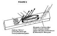
- the articlein which the area of the article including the pattern is light-transmissive, can optionally further include a region underlying the pattern that is capable of directing at least a portion of impingent light toward the semiconductor nanocrystals.
- a regioncan, for example, comprise a waveguide or can be contoured to produce a parabolic effect.
- FIG. 2illustrates an example of an embodiment of the invention in which the material over which the patterned array of semiconductor nanocrystals is disposed acts as a waveguide to collect and guide at least a portion of the ambient light to the patterned array. Enhancing the collected/absorbed light will serve to enhance the contrast of the image under ambient light of all conditions.
- a reflective materialcan be applied beneath the pattern of semiconductor nanocrystals, with the reflective material in light communication with light impinging upon the surface with the nanocrystals.
- the articlefurther includes a cover, coating or layer over at least the portion of the surface upon which the predetermined pattern of semiconductor nanocrystals are disposed to protect the nanocrystals from the environment (e.g., dust, moisture, and the like) and/or scratching or abrasion.
- the covercan further optionally include a lens, prismatic surface, etc. Anti-reflection, light polarizing, and/or other coatings can also optionally be included over the pattern.
Landscapes
- Chemical & Material Sciences (AREA)
- Engineering & Computer Science (AREA)
- Materials Engineering (AREA)
- Organic Chemistry (AREA)
- Physics & Mathematics (AREA)
- General Physics & Mathematics (AREA)
- Theoretical Computer Science (AREA)
- Inorganic Chemistry (AREA)
- Luminescent Compositions (AREA)
- Electroluminescent Light Sources (AREA)
Abstract
Description
(Y—)k-n—(X)-(-L)n
wherein k is 2, 3 or 5, and n is 1, 2, 3, 4 or 5 such that k-n is not less than zero; X is O, S, S═O, SO2, Se, Se═O, N, N═O, P, P═O, As, or As═O; each of Y and L, independently, is aryl, heteroaryl, or a straight or branched C2-12 hydrocarbon chain optionally containing at least one double bond, at least one triple bond, or at least one double bond and one triple bond. The hydrocarbon chain can be optionally substituted with one or more C1-4 alkyl, C2-4 alkenyl, C2-4 alkynyl, C1-4 alkoxy, hydroxyl, halo, amino, nitro, cyano, C3-5 cycloalkyl, 3-5 membered heterocycloalkyl, aryl, heteroaryl, C1-4 alkylcarbonyloxy, C1-4 alkyloxycarbonyl, C1-4 alkylcarbonyl, or formyl. The hydrocarbon chain can also be optionally interrupted by —O—, —S—, —N(Ra)—, —N(Ra)—C(O)—O—, —O—C(O)—N(Ra)—, —N(Ra)—C(O)—N(Rb)—, —O—C(O)—O—, —P(Ra)—, or —P(O)(Ra)—. Each of Ra and Rb, independently, is hydrogen, alkyl, alkenyl, alkynyl, alkoxy, hydroxylalkyl, hydroxyl, or haloalkyl. An aryl group is a substituted or unsubstituted cyclic aromatic group. Examples include phenyl, benzyl, naphthyl, tolyl, anthracyl, nitrophenyl, or halophenyl. A heteroaryl group is an aryl group with one or more heteroatoms in the ring, for instance furyl, pyiridyl, pyrrolyl, phenanthryl.
Claims (41)
Priority Applications (9)
| Application Number | Priority Date | Filing Date | Title |
|---|---|---|---|
| US12/231,887US8642977B2 (en) | 2006-03-07 | 2008-09-05 | Article including semiconductor nanocrystals |
| US12/283,609US8718437B2 (en) | 2006-03-07 | 2008-09-12 | Compositions, optical component, system including an optical component, devices, and other products |
| US12/655,069US8849087B2 (en) | 2006-03-07 | 2009-12-22 | Compositions, optical component, system including an optical component, devices, and other products |
| US13/015,670US9297092B2 (en) | 2005-06-05 | 2011-01-28 | Compositions, optical component, system including an optical component, devices, and other products |
| US14/270,098US9874674B2 (en) | 2006-03-07 | 2014-05-05 | Compositions, optical component, system including an optical component, devices, and other products |
| US14/500,200US9701899B2 (en) | 2006-03-07 | 2014-09-29 | Compositions, optical component, system including an optical component, devices, and other products |
| US15/082,136US9951438B2 (en) | 2006-03-07 | 2016-03-28 | Compositions, optical component, system including an optical component, devices, and other products |
| US15/630,728US10633582B2 (en) | 2006-03-07 | 2017-06-22 | Compositions, optical component, system including an optical component, and other products |
| US15/858,319US10393940B2 (en) | 2006-03-07 | 2017-12-29 | Compositions, optical component, system including an optical component, devices, and other products |
Applications Claiming Priority (3)
| Application Number | Priority Date | Filing Date | Title |
|---|---|---|---|
| US77974006P | 2006-03-07 | 2006-03-07 | |
| PCT/US2007/005589WO2007103310A2 (en) | 2006-03-07 | 2007-03-06 | An article including semiconductor nanocrystals |
| US12/231,887US8642977B2 (en) | 2006-03-07 | 2008-09-05 | Article including semiconductor nanocrystals |
Related Parent Applications (2)
| Application Number | Title | Priority Date | Filing Date |
|---|---|---|---|
| PCT/US2007/005589ContinuationWO2007103310A2 (en) | 2005-06-05 | 2007-03-06 | An article including semiconductor nanocrystals |
| PCT/US2007/005589Continuation-In-PartWO2007103310A2 (en) | 2005-06-05 | 2007-03-06 | An article including semiconductor nanocrystals |
Related Child Applications (2)
| Application Number | Title | Priority Date | Filing Date |
|---|---|---|---|
| PCT/US2008/007902Continuation-In-PartWO2009002512A1 (en) | 2005-06-05 | 2008-06-25 | Compositions, optical component, system including an optical component, devices, and other products |
| US12/283,609Continuation-In-PartUS8718437B2 (en) | 2005-06-05 | 2008-09-12 | Compositions, optical component, system including an optical component, devices, and other products |
Publications (2)
| Publication Number | Publication Date |
|---|---|
| US20090152567A1 US20090152567A1 (en) | 2009-06-18 |
| US8642977B2true US8642977B2 (en) | 2014-02-04 |
Family
ID=38475467
Family Applications (1)
| Application Number | Title | Priority Date | Filing Date |
|---|---|---|---|
| US12/231,887ActiveUS8642977B2 (en) | 2005-06-05 | 2008-09-05 | Article including semiconductor nanocrystals |
Country Status (3)
| Country | Link |
|---|---|
| US (1) | US8642977B2 (en) |
| EP (1) | EP2041478B1 (en) |
| WO (1) | WO2007103310A2 (en) |
Cited By (13)
| Publication number | Priority date | Publication date | Assignee | Title |
|---|---|---|---|---|
| US8981339B2 (en) | 2009-08-14 | 2015-03-17 | Qd Vision, Inc. | Lighting devices, an optical component for a lighting device, and methods |
| US9133388B2 (en) | 2009-04-28 | 2015-09-15 | Qd Vision, Inc. | Optical materials, optical components, and methods |
| US9140844B2 (en) | 2008-05-06 | 2015-09-22 | Qd Vision, Inc. | Optical components, systems including an optical component, and devices |
| US9207385B2 (en) | 2008-05-06 | 2015-12-08 | Qd Vision, Inc. | Lighting systems and devices including same |
| US9252013B2 (en) | 2006-04-07 | 2016-02-02 | Qd Vision, Inc. | Methods and articles including nanomaterial |
| US20170022628A1 (en)* | 2006-03-07 | 2017-01-26 | Qd Vision, Inc. | Compositions, optical component, system including an optical component, devices, and other products |
| US9815996B2 (en) | 2007-06-25 | 2017-11-14 | Samsung Electronics Co., Ltd. | Compositions and methods including depositing nanomaterial |
| US9929325B2 (en) | 2012-06-05 | 2018-03-27 | Samsung Electronics Co., Ltd. | Lighting device including quantum dots |
| US10145539B2 (en) | 2008-05-06 | 2018-12-04 | Samsung Electronics Co., Ltd. | Solid state lighting devices including quantum confined semiconductor nanoparticles, an optical component for a solid state lighting device, and methods |
| US10633582B2 (en) | 2006-03-07 | 2020-04-28 | Samsung Electronics Co., Ltd. | Compositions, optical component, system including an optical component, and other products |
| US10821884B1 (en) | 2019-10-03 | 2020-11-03 | Ford Global Technologies, Llc | Light grille surround and emblem illumination |
| US11464757B2 (en)* | 2009-06-15 | 2022-10-11 | Amarin Pharmaceuticals Ireland Limited | Compositions and methods for lowering triglycerides |
| US20220415221A1 (en)* | 2021-06-29 | 2022-12-29 | Christin Paige MINNOTTE | Light sensitive display system |
Families Citing this family (47)
| Publication number | Priority date | Publication date | Assignee | Title |
|---|---|---|---|---|
| US9297092B2 (en) | 2005-06-05 | 2016-03-29 | Qd Vision, Inc. | Compositions, optical component, system including an optical component, devices, and other products |
| WO2007103310A2 (en) | 2006-03-07 | 2007-09-13 | Qd Vision, Inc. | An article including semiconductor nanocrystals |
| US8845927B2 (en) | 2006-06-02 | 2014-09-30 | Qd Vision, Inc. | Functionalized nanoparticles and method |
| US8718437B2 (en) | 2006-03-07 | 2014-05-06 | Qd Vision, Inc. | Compositions, optical component, system including an optical component, devices, and other products |
| WO2007095061A2 (en)* | 2006-02-09 | 2007-08-23 | Qd Vision, Inc. | Device including semiconductor nanocrystals and a layer including a doped organic material and methods |
| US9874674B2 (en) | 2006-03-07 | 2018-01-23 | Samsung Electronics Co., Ltd. | Compositions, optical component, system including an optical component, devices, and other products |
| US8849087B2 (en) | 2006-03-07 | 2014-09-30 | Qd Vision, Inc. | Compositions, optical component, system including an optical component, devices, and other products |
| WO2007112088A2 (en)* | 2006-03-24 | 2007-10-04 | Qd Vision, Inc. | Hyperspectral imaging device |
| US9212056B2 (en)* | 2006-06-02 | 2015-12-15 | Qd Vision, Inc. | Nanoparticle including multi-functional ligand and method |
| WO2007143227A2 (en)* | 2006-06-10 | 2007-12-13 | Qd Vision, Inc. | Materials,thin films,optical filters, and devices including same |
| WO2008111947A1 (en) | 2006-06-24 | 2008-09-18 | Qd Vision, Inc. | Methods and articles including nanomaterial |
| JP2010508620A (en)* | 2006-09-12 | 2010-03-18 | キユーデイー・ビジヨン・インコーポレーテツド | Electroluminescent display useful for displaying a predetermined pattern |
| WO2008133660A2 (en) | 2006-11-21 | 2008-11-06 | Qd Vision, Inc. | Nanocrystals including a group iiia element and a group va element, method, composition, device and other prodcucts |
| WO2008063653A1 (en) | 2006-11-21 | 2008-05-29 | Qd Vision, Inc. | Semiconductor nanocrystals and compositions and devices including same |
| WO2008063652A1 (en) | 2006-11-21 | 2008-05-29 | Qd Vision, Inc. | Blue emitting semiconductor nanocrystals and compositions and devices including same |
| WO2008063658A2 (en)* | 2006-11-21 | 2008-05-29 | Qd Vision, Inc. | Semiconductor nanocrystals and compositions and devices including same |
| US20080172197A1 (en)* | 2007-01-11 | 2008-07-17 | Motorola, Inc. | Single laser multi-color projection display with quantum dot screen |
| US8836212B2 (en) | 2007-01-11 | 2014-09-16 | Qd Vision, Inc. | Light emissive printed article printed with quantum dot ink |
| US7989153B2 (en)* | 2007-07-11 | 2011-08-02 | Qd Vision, Inc. | Method and apparatus for selectively patterning free standing quantum DOT (FSQDT) polymer composites |
| WO2009014707A2 (en) | 2007-07-23 | 2009-01-29 | Qd Vision, Inc. | Quantum dot light enhancement substrate and lighting device including same |
| US8128249B2 (en) | 2007-08-28 | 2012-03-06 | Qd Vision, Inc. | Apparatus for selectively backlighting a material |
| US7984989B2 (en)* | 2008-02-07 | 2011-07-26 | Gruber Jake A | Retinal melatonin suppressor comprising a filter layer |
| US7841714B2 (en) | 2008-02-07 | 2010-11-30 | Quantum Modulation Scientific Inc. | Retinal melatonin suppressor |
| WO2009145813A1 (en) | 2008-03-04 | 2009-12-03 | Qd Vision, Inc. | Particles including nanoparticles, uses thereof, and methods |
| US9525148B2 (en) | 2008-04-03 | 2016-12-20 | Qd Vision, Inc. | Device including quantum dots |
| KR20110008206A (en) | 2008-04-03 | 2011-01-26 | 큐디 비젼, 인크. | Light Emitting Device Including Quantum Dots |
| US20100264371A1 (en)* | 2009-03-19 | 2010-10-21 | Nick Robert J | Composition including quantum dots, uses of the foregoing, and methods |
| US9346998B2 (en) | 2009-04-23 | 2016-05-24 | The University Of Chicago | Materials and methods for the preparation of nanocomposites |
| WO2011031876A1 (en) | 2009-09-09 | 2011-03-17 | Qd Vision, Inc. | Formulations including nanoparticles |
| CN102482457B (en) | 2009-09-09 | 2015-04-15 | Qd视光有限公司 | Particles including nanoparticles, uses thereof, and methods |
| JP5737011B2 (en) | 2011-01-18 | 2015-06-17 | 日本電気硝子株式会社 | LIGHT EMITTING DEVICE, LIGHT EMITTING DEVICE CELL, AND LIGHT EMITTING DEVICE MANUFACTURING METHOD |
| KR101210066B1 (en) | 2011-01-31 | 2012-12-07 | 엘지이노텍 주식회사 | Light conversion member and display device having the same |
| WO2012158832A2 (en) | 2011-05-16 | 2012-11-22 | Qd Vision, Inc. | Method for preparing semiconductor nanocrystals |
| KR101273099B1 (en) | 2011-05-24 | 2013-06-13 | 엘지이노텍 주식회사 | Optical sheet, display device having the same and method of fabricating the same |
| KR101305696B1 (en) | 2011-07-14 | 2013-09-09 | 엘지이노텍 주식회사 | Display device and optical member |
| KR20130009020A (en) | 2011-07-14 | 2013-01-23 | 엘지이노텍 주식회사 | Optical member, display device having the same and method of fabricating the same |
| KR101241549B1 (en) | 2011-07-18 | 2013-03-11 | 엘지이노텍 주식회사 | Optical member, display device having the same and method of fabricating the same |
| KR101262520B1 (en) | 2011-07-18 | 2013-05-08 | 엘지이노텍 주식회사 | Optical member and display device including same |
| KR101893494B1 (en) | 2011-07-18 | 2018-08-30 | 엘지이노텍 주식회사 | Optical member and display device having the same |
| KR101294415B1 (en) | 2011-07-20 | 2013-08-08 | 엘지이노텍 주식회사 | Optical member and display device having the same |
| WO2013028253A1 (en) | 2011-08-19 | 2013-02-28 | Qd Vision, Inc. | Semiconductor nanocrystals and methods |
| GB2494659A (en) | 2011-09-14 | 2013-03-20 | Sharp Kk | Nitride nanoparticles with high quantum yield and narrow luminescence spectrum. |
| KR101251815B1 (en) | 2011-11-07 | 2013-04-09 | 엘지이노텍 주식회사 | Optical sheet and display device having the same |
| KR101980195B1 (en) | 2012-05-16 | 2019-05-21 | 삼성전자주식회사 | Transistor having sulfur doped zinc oxynitride and method of manufacturing the same |
| KR20150063529A (en)* | 2012-10-04 | 2015-06-09 | 나노코 테크놀로지스 리미티드 | Illuminated signage using quantum dots |
| US20160200974A1 (en)* | 2015-01-12 | 2016-07-14 | The Board Of Trustees Of The University Of Illinois | Brightness equalized quantum dots |
| CN107894501A (en)* | 2017-11-06 | 2018-04-10 | 深圳先进技术研究院 | A kind of contact lens kit and its application |
Citations (328)
| Publication number | Priority date | Publication date | Assignee | Title |
|---|---|---|---|---|
| US3510732A (en) | 1968-04-22 | 1970-05-05 | Gen Electric | Solid state lamp having a lens with rhodamine or fluorescent material dispersed therein |
| US3774086A (en) | 1972-09-25 | 1973-11-20 | Gen Electric | Solid state lamp having visible-emitting phosphor at edge of infrated-emitting element |
| US3825792A (en) | 1973-07-03 | 1974-07-23 | Westinghouse Electric Corp | Novel discharge lamp and coating |
| US3875456A (en) | 1972-04-04 | 1975-04-01 | Hitachi Ltd | Multi-color semiconductor lamp |
| US4035686A (en) | 1976-02-13 | 1977-07-12 | Atkins & Merrill, Incorported | Narrow emission spectrum lamp using electroluminescent and photoluminescent materials |
| US4082889A (en) | 1976-01-28 | 1978-04-04 | International Business Machines Corporation | Luminescent material, luminescent thin film therefrom, and optical display device therewith |
| US4130343A (en) | 1977-02-22 | 1978-12-19 | Bell Telephone Laboratories, Incorporated | Coupling arrangements between a light-emitting diode and an optical fiber waveguide and between an optical fiber waveguide and a semiconductor optical detector |
| US4366407A (en) | 1979-06-05 | 1982-12-28 | Duro-Test Corporation | Incandescent lamp with selective color filter |
| US4377750A (en) | 1979-10-11 | 1983-03-22 | Siemens Aktiengesellschaft | Passive display device |
| US4382272A (en) | 1979-11-15 | 1983-05-03 | Siemens Aktiengesellschaft | Colored lamp |
| US4394068A (en) | 1979-03-20 | 1983-07-19 | Siemens Aktiengesellschaft | Fluorescently activated display device with improved sensitivity |
| GB2147542A (en) | 1983-10-05 | 1985-05-15 | Fade In Products | Printed articles |
| US4608301A (en) | 1983-08-02 | 1986-08-26 | Fuji Photo Film Co., Ltd. | Radiographic intensifying screen |
| US4652464A (en) | 1982-08-23 | 1987-03-24 | Ludlum John P | Printing fine art with fluorescent and non-fluorescent colorants |
| US4719386A (en) | 1984-11-24 | 1988-01-12 | Matsushita Electric Works, Ltd. | Photoconverter and lamp utilizing multi-quantum emission |
| US4738798A (en) | 1987-01-08 | 1988-04-19 | E. I. Du Pont De Nemours And Company | Semiconductor compositions |
| US4766526A (en) | 1985-07-15 | 1988-08-23 | Futaba Denshi Kogyo Kabushiki Kaisha | Light source |
| US4772885A (en) | 1984-11-22 | 1988-09-20 | Ricoh Company, Ltd. | Liquid crystal color display device |
| US4780752A (en) | 1981-05-04 | 1988-10-25 | Telefunken Electronic Gmbh | Luminescent semiconductor component |
| US4820016A (en) | 1986-02-21 | 1989-04-11 | American Telephone And Telegraph Company, At&T Bell Laboratories | Waveguide-containing communications and sensing systems |
| EP0328202A2 (en) | 1988-02-12 | 1989-08-16 | Philips Electronics Uk Limited | Method of forming a quantum dot structure |
| US4931692A (en) | 1987-10-14 | 1990-06-05 | Canon Kabushiki Kaisha | Luminescing member, process for preparation thereof, and electroluminescent device employing same |
| US5064718A (en) | 1989-04-27 | 1991-11-12 | Imperial Chemical Industries, Plc | Inorganic particles |
| US5077147A (en) | 1989-05-31 | 1991-12-31 | Pioneer Electronic Corporation | Luminescent screen |
| US5091115A (en) | 1989-04-17 | 1992-02-25 | Hoya Corporation | Semiconductor-containing glass and method for producing same |
| US5093286A (en) | 1989-12-18 | 1992-03-03 | Hoya Corporation | Semiconductor-containing glass and method of producing the same |
| US5132051A (en) | 1989-02-24 | 1992-07-21 | E. I. Du Pont De Nemours And Company | Iii-v semiconductors in rigid matrices |
| US5208462A (en) | 1991-12-19 | 1993-05-04 | Allied-Signal Inc. | Wide bandwidth solid state optical source |
| US5243457A (en) | 1991-02-05 | 1993-09-07 | American Ingenuity, Inc. | Material with enhanced visibility characteristics |
| US5260957A (en) | 1992-10-29 | 1993-11-09 | The Charles Stark Draper Laboratory, Inc. | Quantum dot Laser |
| US5294870A (en) | 1991-12-30 | 1994-03-15 | Eastman Kodak Company | Organic electroluminescent multicolor image display device |
| US5300783A (en) | 1992-05-26 | 1994-04-05 | American Ingenuity, Inc. | Layered reflecting and luminous material |
| US5422489A (en) | 1994-01-24 | 1995-06-06 | Bhargava; Rameshwar N. | Light emitting device |
| US5434878A (en) | 1994-03-18 | 1995-07-18 | Brown University Research Foundation | Optical gain medium having doped nanocrystals of semiconductors and also optical scatterers |
| US5442254A (en) | 1993-05-04 | 1995-08-15 | Motorola, Inc. | Fluorescent device with quantum contained particle screen |
| US5455489A (en) | 1994-04-11 | 1995-10-03 | Bhargava; Rameshwar N. | Displays comprising doped nanocrystal phosphors |
| US5470910A (en) | 1991-10-10 | 1995-11-28 | Institut Fuer Neue Materialien Gemeinnuetzige Gmbh | Composite materials containing nanoscalar particles, process for producing them and their use for optical components |
| US5504661A (en) | 1994-07-05 | 1996-04-02 | Ford Motor Company | Translucent fluorescent filter for display panels |
| US5527386A (en) | 1993-10-28 | 1996-06-18 | Manfred R. Kuehnle | Composite media with selectable radiation-transmission properties |
| US5534056A (en) | 1993-10-28 | 1996-07-09 | Manfred R. Kuehnle | Composite media with selectable radiation-transmission properties |
| US5586879A (en) | 1994-07-05 | 1996-12-24 | Ford Motor Company | Fluorescent electroluminescent lamp |
| US5716679A (en) | 1991-09-13 | 1998-02-10 | Institut Fur Neue Materialien Gemeinnutzige Gmbh | Optical elements containing nanoscaled particles and having an embossed surface and process for their preparation |
| US5717289A (en) | 1996-01-30 | 1998-02-10 | Nec Corporation | Thin film electroluminescent element easily regulating emitted light to white |
| US5777433A (en) | 1996-07-11 | 1998-07-07 | Hewlett-Packard Company | High refractive index package material and a light emitting device encapsulated with such material |
| US5813753A (en) | 1997-05-27 | 1998-09-29 | Philips Electronics North America Corporation | UV/blue led-phosphor device with efficient conversion of UV/blues light to visible light |
| US5813752A (en) | 1997-05-27 | 1998-09-29 | Philips Electronics North America Corporation | UV/blue LED-phosphor device with short wave pass, long wave pass band pass and peroit filters |
| US5830529A (en) | 1996-01-11 | 1998-11-03 | Ross; Gregory E. | Perimeter coating alignment |
| US5847507A (en) | 1997-07-14 | 1998-12-08 | Hewlett-Packard Company | Fluorescent dye added to epoxy of light emitting diode lens |
| US5874803A (en) | 1997-09-09 | 1999-02-23 | The Trustees Of Princeton University | Light emitting device with stack of OLEDS and phosphor downconverter |
| US5881200A (en) | 1994-09-29 | 1999-03-09 | British Telecommunications Public Limited Company | Optical fibre with quantum dots |
| US5882779A (en) | 1994-11-08 | 1999-03-16 | Spectra Science Corporation | Semiconductor nanocrystal display materials and display apparatus employing same |
| US5909081A (en) | 1995-02-06 | 1999-06-01 | Idemitsu Kosan Co., Ltd. | Multi-color light emission apparatus with organic electroluminescent device |
| US5917279A (en) | 1995-11-20 | 1999-06-29 | Bayer Aktiengesllschaft | Intermediate layer in electroluminescent arrangements containing finely divided inorganic particles |
| US5955528A (en) | 1996-07-04 | 1999-09-21 | Fuji Xerox Co., Ltd. | Polymeric composite material and process for manufacturing the same |
| US5959316A (en) | 1998-09-01 | 1999-09-28 | Hewlett-Packard Company | Multiple encapsulation of phosphor-LED devices |
| US5962971A (en) | 1997-08-29 | 1999-10-05 | Chen; Hsing | LED structure with ultraviolet-light emission chip and multilayered resins to generate various colored lights |
| US5988822A (en) | 1997-11-21 | 1999-11-23 | 3M Innovative Properties Company | Luminous retroreflective sheeting and method for making same |
| US6023371A (en) | 1997-06-09 | 2000-02-08 | Tdk Corporation | Color conversion material, and organic electroluminescent color display using the same |
| US6048616A (en) | 1993-04-21 | 2000-04-11 | Philips Electronics N.A. Corp. | Encapsulated quantum sized doped semiconductor particles and method of manufacturing same |
| US6066861A (en) | 1996-09-20 | 2000-05-23 | Siemens Aktiengesellschaft | Wavelength-converting casting composition and its use |
| US6117529A (en) | 1996-12-18 | 2000-09-12 | Gunther Leising | Organic electroluminescence devices and displays |
| US6166856A (en) | 1997-06-16 | 2000-12-26 | 3M Innovative Properties Company | Self light-emitting retroreflective sheet and method for producing the same |
| US20010001207A1 (en) | 1996-07-29 | 2001-05-17 | Nichia Kagaku Kogyo Kabushiki Kaisha | Light emitting device and display |
| US6236493B1 (en) | 1996-04-04 | 2001-05-22 | Institut für Neue Materialien Gemeinnützige GmbH | Optical components with a graded-index structure, and method of manufacturing such components |
| US6249372B1 (en) | 1998-09-10 | 2001-06-19 | Fuji Electric Co., Ltd. | Fluorescent conversion filter and color display device using the same |
| WO2001066997A2 (en) | 2000-03-06 | 2001-09-13 | Teledyne Lighting And Display Products, Inc. | Lighting apparatus having quantum dot layer |
| US6319426B1 (en) | 1998-09-18 | 2001-11-20 | Massachusetts Institute Of Technology | Water-soluble fluorescent semiconductor nanocrystals |
| US6322901B1 (en) | 1997-11-13 | 2001-11-27 | Massachusetts Institute Of Technology | Highly luminescent color-selective nano-crystalline materials |
| US20020021003A1 (en) | 1998-12-31 | 2002-02-21 | Mcgrew Stephen P. | Quantum dot security device and method |
| US6358652B1 (en) | 1999-07-22 | 2002-03-19 | Fuji Electric Co., Ltd. | Fluorescent conversion filter and organic light-emitting device equipped with the fluorescent conversion filter |
| US20020071948A1 (en) | 2000-10-09 | 2002-06-13 | Daniel-Gordon Duff | Composite particles |
| JP2002216962A (en) | 2001-01-17 | 2002-08-02 | Fuji Electric Co Ltd | Color conversion filter substrate, and color conversion color display including color conversion filter substrate |
| US6464898B1 (en) | 1998-11-20 | 2002-10-15 | Idemitsu Kosan Co., Ltd. | Fluorescence conversion medium and display device comprising it |
| US6482664B1 (en) | 2000-07-28 | 2002-11-19 | Jeong-Hoon Lee | Method for manufacturing white light-emitting diodes |
| US6493051B2 (en) | 1999-12-06 | 2002-12-10 | Lg Philips Lcd Co., Ltd. | Transflective liquid crystal display device |
| US20020186921A1 (en) | 2001-06-06 | 2002-12-12 | Schumacher Lynn C. | Multiwavelength optical fiber devices |
| US6501091B1 (en) | 1998-04-01 | 2002-12-31 | Massachusetts Institute Of Technology | Quantum dot white and colored light emitting diodes |
| US6515314B1 (en) | 2000-11-16 | 2003-02-04 | General Electric Company | Light-emitting device with organic layer doped with photoluminescent material |
| US6565770B1 (en) | 2000-11-17 | 2003-05-20 | Flex Products, Inc. | Color-shifting pigments and foils with luminescent coatings |
| US6576155B1 (en) | 1998-11-10 | 2003-06-10 | Biocrystal, Ltd. | Fluorescent ink compositions comprising functionalized fluorescent nanocrystals |
| US6577073B2 (en) | 2000-05-31 | 2003-06-10 | Matsushita Electric Industrial Co., Ltd. | Led lamp |
| US6576291B2 (en) | 2000-12-08 | 2003-06-10 | Massachusetts Institute Of Technology | Preparation of nanocrystallites |
| US20030107688A1 (en) | 2000-12-25 | 2003-06-12 | Machio Yamagishi | Image display |
| US6580545B2 (en) | 2001-04-19 | 2003-06-17 | E Ink Corporation | Electrochromic-nanoparticle displays |
| US6586096B2 (en) | 2000-12-22 | 2003-07-01 | Eastman Kodak Company | Polymethylmethacrylate nanocomposite optical article and method of making same |
| US6600175B1 (en) | 1996-03-26 | 2003-07-29 | Advanced Technology Materials, Inc. | Solid state white light emitter and display using same |
| US20030151700A1 (en) | 2001-12-20 | 2003-08-14 | Carter Susan A. | Screen printable electroluminescent polymer ink |
| US6608439B1 (en) | 1998-09-22 | 2003-08-19 | Emagin Corporation | Inorganic-based color conversion matrix element for organic color display devices and method of fabrication |
| US20030156425A1 (en) | 1996-06-13 | 2003-08-21 | Turnbull Robert R. | Light emitting assembly |
| US20030160260A1 (en) | 2002-02-28 | 2003-08-28 | Fuji Photo Film Co., Ltd. | Light-emitting element and method of producing the same |
| US6637924B2 (en) | 2000-11-15 | 2003-10-28 | Teledyne Lighting And Display Products, Inc. | Strip lighting apparatus and method |
| US20030211288A1 (en) | 2002-05-13 | 2003-11-13 | Philippe Schottland | Plastics articles such as bottles with visual effect |
| US6650044B1 (en) | 2000-10-13 | 2003-11-18 | Lumileds Lighting U.S., Llc | Stenciling phosphor layers on light emitting diodes |
| US6653778B1 (en) | 1999-09-24 | 2003-11-25 | Fuji Electric Co., Ltd. | Fluorescent color conversion film, fluorescent color conversion filter using the conversion film, and organic light-emitting device equipped with the conversion filter |
| US6656566B1 (en) | 1997-04-15 | 2003-12-02 | 3M Innovative Properties Company | Retroreflective luminescent articles |
| US20030227249A1 (en) | 2002-06-07 | 2003-12-11 | Lumileds Lighting, U.S., Llc | Light-emitting devices utilizing nanoparticles |
| US6677610B2 (en) | 2001-04-17 | 2004-01-13 | Samsung Electronics Co., Ltd. | Light-emitting device and display apparatus using the same |
| US20040007169A1 (en) | 2002-01-28 | 2004-01-15 | Mitsubishi Chemical Corporation | Semiconductor nanoparticles and thin film containing the same |
| US6703781B2 (en) | 2002-05-21 | 2004-03-09 | Durel Corporation | El lamp with light scattering particles in cascading layer |
| US6710911B2 (en) | 2001-03-02 | 2004-03-23 | Evident Technologies | Optical wavelength converter |
| US6710366B1 (en) | 2001-08-02 | 2004-03-23 | Ultradots, Inc. | Nanocomposite materials with engineered properties |
| US6731359B1 (en) | 1999-10-05 | 2004-05-04 | Dai Nippon Printing Co., Ltd. | Color filters including light scattering fine particles and colorants |
| US6734465B1 (en) | 2001-11-19 | 2004-05-11 | Nanocrystals Technology Lp | Nanocrystalline based phosphors and photonic structures for solid state lighting |
| US20040095658A1 (en) | 2002-09-05 | 2004-05-20 | Nanosys, Inc. | Nanocomposites |
| US6744077B2 (en) | 2002-09-27 | 2004-06-01 | Lumileds Lighting U.S., Llc | Selective filtering of wavelength-converted semiconductor light emitting devices |
| US20040118448A1 (en) | 2002-09-05 | 2004-06-24 | Nanosys, Inc. | Nanostructure and nanocomposite based compositions and photovoltaic devices |
| US6777531B2 (en) | 2000-04-26 | 2004-08-17 | Sony International (Europe) Gmbh | End-capped polyfluorenes, films and devices based thereon |
| US6777706B1 (en) | 1998-07-14 | 2004-08-17 | Cambridge Display Technologies | Optical devices |
| US6781148B2 (en) | 2000-07-24 | 2004-08-24 | Tdk Corporation | Light emitting device |
| US6784603B2 (en)* | 2001-07-20 | 2004-08-31 | Teledyne Lighting And Display Products, Inc. | Fluorescent lighting apparatus |
| US6791259B1 (en) | 1998-11-30 | 2004-09-14 | General Electric Company | Solid state illumination system containing a light emitting diode, a light scattering material and a luminescent material |
| US20040178338A1 (en) | 2000-04-06 | 2004-09-16 | Quantum Dot Corporation, A California Corporation | Differentiable spectral bar code methods and systems |
| US6793755B2 (en) | 2001-06-01 | 2004-09-21 | Interactive Packaging Group, Ltd. | Method and machine for placement of multiple labels |
| US6794686B2 (en) | 2002-06-06 | 2004-09-21 | Harvatek Corporation | White light source |
| US20040203170A1 (en)* | 1998-11-10 | 2004-10-14 | Emilio Barbera-Guillem | Methods for identification and verification |
| US6812500B2 (en) | 1996-06-26 | 2004-11-02 | Osram Opto Semiconductors Gmbh & Co. Ohg. | Light-radiating semiconductor component with a luminescence conversion element |
| US6819845B2 (en) | 2001-08-02 | 2004-11-16 | Ultradots, Inc. | Optical devices with engineered nonlinear nanocomposite materials |
| US6821559B2 (en) | 1997-10-02 | 2004-11-23 | Chris Eberspacher | Method of forming particulate materials for thin-film solar cells |
| US20040233139A1 (en) | 2002-10-08 | 2004-11-25 | Masaaki Asano | Color conversion media and el-display using the same |
| US6827769B2 (en) | 2001-05-10 | 2004-12-07 | Pitney Bowes Inc. | Photosensitive optically variable ink heterogeneous compositions for ink jet printing |
| US6830835B2 (en) | 2002-11-12 | 2004-12-14 | 3M Innovative Properties Company | Display film |
| US6838743B2 (en) | 1996-06-19 | 2005-01-04 | Matsushita Electric Industrial Co., Ltd. | Optoelectronic material, device using the same and method for manufacturing optoelectronic material |
| US6841785B2 (en) | 2002-05-16 | 2005-01-11 | Nd Holdings, Inc. | Photoluminescent floor tile |
| US20050009224A1 (en) | 2003-06-20 | 2005-01-13 | The Regents Of The University Of California | Nanowire array and nanowire solar cells and methods for forming the same |
| US20050012076A1 (en) | 2002-09-20 | 2005-01-20 | Sharp Kabushiki Kaisha | Fluorescent member, and illumination device and display device including the same |
| US6849109B2 (en) | 1996-09-03 | 2005-02-01 | Nanoproducts Corporation | Inorganic dopants, inks and related nanotechnology |
| US6858470B1 (en) | 2003-10-08 | 2005-02-22 | St Assembly Test Services Ltd. | Method for fabricating semiconductor packages, and leadframe assemblies for the fabrication thereof |
| US6864626B1 (en) | 1998-06-03 | 2005-03-08 | The Regents Of The University Of California | Electronic displays using optically pumped luminescent semiconductor nanocrystals |
| US6876796B2 (en) | 2002-01-30 | 2005-04-05 | Photon-X, Llc | Nanocomposite microresonators |
| US6885033B2 (en) | 2003-03-10 | 2005-04-26 | Cree, Inc. | Light emitting devices for light conversion and methods and semiconductor chips for fabricating the same |
| US20050088079A1 (en) | 2002-03-01 | 2005-04-28 | Daniels John J. | Organic and inorganic light active devices and methods for making the same |
| US6887332B1 (en) | 2000-04-21 | 2005-05-03 | International Business Machines Corporation | Patterning solution deposited thin films with self-assembled monolayers |
| US20050093422A1 (en) | 2003-10-31 | 2005-05-05 | Chien-Yuan Wang | White light-emitting device |
| US6891330B2 (en) | 2002-03-29 | 2005-05-10 | General Electric Company | Mechanically flexible organic electroluminescent device with directional light emission |
| US6903505B2 (en) | 2001-12-17 | 2005-06-07 | General Electric Company | Light-emitting device with organic electroluminescent material and photoluminescent materials |
| US20050133087A1 (en)* | 2001-10-24 | 2005-06-23 | The Regents Of The University Of California | Semiconductor-nanocrystal/conjugated polymer thin films |
| US20050135079A1 (en) | 2003-12-18 | 2005-06-23 | Yin Chua Janet B. | Flash module with quantum dot light conversion |
| US20050134723A1 (en) | 2003-12-18 | 2005-06-23 | Lee Kian S. | Flash lighting for image acquisition |
| US20050142343A1 (en) | 2002-02-01 | 2005-06-30 | Holger Winkler | Moulded bodies consisting of core-shell particles |
| US20050139852A1 (en) | 2003-12-26 | 2005-06-30 | Hsueh-Shih Chen | Light emitting diode |
| US6914106B2 (en) | 2003-07-23 | 2005-07-05 | Eastman Kodak Company | Polymer microspheres containing latent colorants and method of preparation |
| US6913830B2 (en) | 2003-08-14 | 2005-07-05 | Ppg Industries Ohio, Inc. | Coating compositions containing semiconductor colorants |
| US20050164227A1 (en) | 2003-08-08 | 2005-07-28 | Nof Corporation | Method for preparing semiconductor nanocrystals having core-shell structure |
| US6924596B2 (en) | 2001-11-01 | 2005-08-02 | Nichia Corporation | Light emitting apparatus provided with fluorescent substance and semiconductor light emitting device, and method of manufacturing the same |
| US20050180680A1 (en) | 2004-02-13 | 2005-08-18 | Kong Eric S. | Integrated optical devices and method of fabrication thereof |
| US20050230693A1 (en) | 2004-04-14 | 2005-10-20 | Genesis Photonics Inc. | Single-chip LED with three luminescent spectrums of red, blue and green wavelengths |
| US6957608B1 (en) | 2002-08-02 | 2005-10-25 | Kovio, Inc. | Contact print methods |
| US20050236556A1 (en) | 2004-04-19 | 2005-10-27 | Edward Sargent | Optically-regulated optical emission using colloidal quantum dot nanocrystals |
| US20050258418A1 (en)* | 2004-03-08 | 2005-11-24 | Steckel Jonathan S | Blue light emitting semiconductor nanocrystal materials |
| US20050265935A1 (en)* | 2004-05-28 | 2005-12-01 | Hollingsworth Jennifer A | Semiconductor nanocrystal quantum dots and metallic nanocrystals as UV blockers and colorants for suncreens and/or sunless tanning compositions |
| US20050265404A1 (en) | 2004-05-28 | 2005-12-01 | Ian Ashdown | Luminance enhancement apparatus and method |
| US20050275615A1 (en) | 2004-06-09 | 2005-12-15 | Eastman Kodak Company | Display device using vertical cavity laser arrays |
| US20050279949A1 (en) | 1999-05-17 | 2005-12-22 | Applera Corporation | Temperature control for light-emitting diode stabilization |
| US20060003114A1 (en) | 2003-06-09 | 2006-01-05 | Howard Enlow | Multilayer film |
| US20060003097A1 (en) | 2003-08-06 | 2006-01-05 | Andres Ronald P | Fabrication of nanoparticle arrays |
| US20060002101A1 (en) | 2004-06-30 | 2006-01-05 | Wheatley John A | Phosphor based illumination system having a long pass reflector and method of making same |
| US20060003156A1 (en) | 2004-06-25 | 2006-01-05 | Akira Masutani | Method of controlling light diffusion and/or reducing glare from a surface |
| US20060001036A1 (en) | 2004-07-02 | 2006-01-05 | Gelcore, Llc | LED-based edge lit illumination system |
| US6984297B2 (en) | 1999-10-08 | 2006-01-10 | NMI Naturwissenschaftliches und Medizinisches Institut an der Universität Tübingen | Device for taking measurements of cells which are contained in a liquid environment |
| US20060012853A1 (en)* | 2004-07-14 | 2006-01-19 | Luigi Tallone | Low cost optical amplifier |
| US20060024525A1 (en) | 2004-07-29 | 2006-02-02 | Hye-In Jeong | Organic electroluminescent device |
| US20060034065A1 (en) | 2004-08-10 | 2006-02-16 | Innovalight, Inc. | Light strips for lighting and backlighting applications |
| US7005667B2 (en) | 2003-08-28 | 2006-02-28 | Genesis Photonics, Inc. | Broad-spectrum A1(1-x-y)InyGaxN light emitting diodes and solid state white light emitting devices |
| US7005669B1 (en) | 2001-08-02 | 2006-02-28 | Ultradots, Inc. | Quantum dots, nanocomposite materials with quantum dots, devices with quantum dots, and related fabrication methods |
| US7008559B2 (en) | 2001-06-06 | 2006-03-07 | Nomadics, Inc. | Manganese doped upconversion luminescence nanoparticles |
| JP2006073869A (en) | 2004-09-03 | 2006-03-16 | Toppan Printing Co Ltd | Stencil mask and stencil mask blanks |
| US20060063289A1 (en) | 2004-09-21 | 2006-03-23 | Negley Gerald H | Methods of coating semiconductor light emitting elements by evaporating solvent from a suspension |
| US20060060862A1 (en) | 2001-02-09 | 2006-03-23 | Massachusetts Institute Of Technology | Composite material including nanocrystals and methods of making |
| US20060066210A1 (en) | 2004-09-30 | 2006-03-30 | Ng Kee Y | Light source with wavelength converting material |
| US20060068154A1 (en) | 2004-01-15 | 2006-03-30 | Nanosys, Inc. | Nanocrystal doped matrixes |
| US20060081862A1 (en) | 2004-10-14 | 2006-04-20 | Chua Janet B Y | Device and method for emitting output light using quantum dots and non-quantum fluorescent material |
| US7040774B2 (en) | 2003-05-23 | 2006-05-09 | Goldeneye, Inc. | Illumination systems utilizing multiple wavelength light recycling |
| US7042020B2 (en) | 2003-02-14 | 2006-05-09 | Cree, Inc. | Light emitting device incorporating a luminescent material |
| US7045956B2 (en) | 2002-05-06 | 2006-05-16 | Osram Opto Semiconductors Gmbh | Light emitting diode with wavelength conversion |
| US7046439B2 (en) | 2003-05-22 | 2006-05-16 | Eastman Kodak Company | Optical element with nanoparticles |
| US20060105483A1 (en) | 2004-11-18 | 2006-05-18 | Leatherdale Catherine A | Encapsulated light emitting diodes and methods of making |
| US20060103589A1 (en) | 2004-11-18 | 2006-05-18 | Chua Janet Bee Y | Device and method for providing illuminating light using quantum dots |
| US20060113895A1 (en) | 2004-11-30 | 2006-06-01 | Baroky Tajul A | Light emitting device with multiple layers of quantum dots and method for making the device |
| US20060128845A1 (en) | 2004-08-06 | 2006-06-15 | Emrick Todd S | Quantum dots tailored with electronically-active polymers |
| US7065285B2 (en) | 2003-12-01 | 2006-06-20 | Lucent Technologies Inc. | Polymeric compositions comprising quantum dots, optical devices comprising these compositions and methods for preparing same |
| US7066623B2 (en) | 2003-12-19 | 2006-06-27 | Soo Ghee Lee | Method and apparatus for producing untainted white light using off-white light emitting diodes |
| US7070300B2 (en) | 2004-06-04 | 2006-07-04 | Philips Lumileds Lighting Company, Llc | Remote wavelength conversion in an illumination device |
| US20060147703A1 (en) | 2004-12-30 | 2006-07-06 | Walker Christopher B Jr | High refractive index monomers for optical applications |
| US20060145599A1 (en) | 2005-01-04 | 2006-07-06 | Reza Stegamat | OLEDs with phosphors |
| US20060157686A1 (en) | 2005-01-20 | 2006-07-20 | Samsung Electronics Co., Ltd. | Quantum dot phosphor for light emitting diode and method of preparing the same |
| US20060160209A1 (en)* | 2004-10-13 | 2006-07-20 | U.S. Genomics, Inc. | Systems and methods for measurement optimization |
| US20060157720A1 (en) | 2005-01-11 | 2006-07-20 | Bawendi Moungi G | Nanocrystals including III-V semiconductors |
| US20060169971A1 (en) | 2005-02-03 | 2006-08-03 | Kyung-Sang Cho | Energy conversion film and quantum dot film comprising quantum dot compound, energy conversion layer including the quantum dot film, and solar cell including the energy conversion layer |
| US7091656B2 (en) | 2001-04-20 | 2006-08-15 | Nichia Corporation | Light emitting device |
| US7090355B2 (en) | 2003-05-19 | 2006-08-15 | Superimaging, Inc. | System and method for a transparent color image display utilizing fluorescence conversion of nano particles and molecules |
| US20060196375A1 (en) | 2004-10-22 | 2006-09-07 | Seth Coe-Sullivan | Method and system for transferring a patterned material |
| US20060199886A1 (en) | 2005-03-02 | 2006-09-07 | Aps Laboratory | Metal phosphate sols, metal nanoparticles, metal-chalcogenide nanoparticles, and nanocomposites made therefrom |
| US20060197437A1 (en) | 2005-03-02 | 2006-09-07 | Osram Opto Semiconductors Gmbh | Novel method to generate high efficient devices which emit high quality light for illumination |
| US20060204676A1 (en) | 2005-03-11 | 2006-09-14 | Jones Clinton L | Polymerizable composition comprising low molecular weight organic component |
| US20060204679A1 (en) | 2005-03-11 | 2006-09-14 | 3M Innovative Properties Company | Polymerizable compositions comprising nanoparticles |
| US20060210726A1 (en) | 2004-06-17 | 2006-09-21 | 3M Innovative Properties Company | Optical film assembly and display device |
| US20060215958A1 (en) | 2004-11-17 | 2006-09-28 | Yeo Terence E | Enhanced electroluminescent sign |
| US20060214903A1 (en) | 2003-02-21 | 2006-09-28 | Sanyo Electric Co., Ltd. | Light-emitting device and display |
| US20060216508A1 (en) | 2005-03-24 | 2006-09-28 | 3M Innovative Properties Company | Polymer nanocomposite having surface modified nanoparticles and methods of preparing same |
| US20060221021A1 (en) | 2005-04-01 | 2006-10-05 | Hajjar Roger A | Display systems having screens with optical fluorescent materials |
| US7123796B2 (en) | 2003-12-08 | 2006-10-17 | University Of Cincinnati | Light emissive display based on lightwave coupling |
| US20060238671A1 (en) | 2005-04-20 | 2006-10-26 | Samsung Electronics Co., Ltd. | Photo-luminescence liquid crystal display |
| US20060240258A1 (en) | 2004-11-12 | 2006-10-26 | Keiichi Sato | Semiconductor nanoparticle having high luminescence properties |
| US20060238103A1 (en) | 2005-04-25 | 2006-10-26 | Samsung Electronics Co., Ltd. | Photo-luminescence liquid crystal display |
| US20060240590A1 (en)* | 2004-11-09 | 2006-10-26 | The Research Foundation Of State University Of New York | Controlled synthesis of nanowires, nanodiscs, and nanostructured materials using liquid crystalline templates |
| US7129515B2 (en) | 2000-07-18 | 2006-10-31 | Sony Corporation | Lighting system |
| US20060245710A1 (en) | 2005-04-29 | 2006-11-02 | Borrelli Nicholas F | Optical waveguides containing quantum dot guiding layers and methods of manufacture |
| US20060244367A1 (en) | 2005-04-27 | 2006-11-02 | Im Seoung-Jae | Photoluminescent liquid crystal display |
| US7135816B2 (en) | 2003-02-20 | 2006-11-14 | Fuji Electric Co., Ltd. | Color conversion filter and color conversion color display having the same |
| US7144131B2 (en) | 2004-09-29 | 2006-12-05 | Advanced Optical Technologies, Llc | Optical system using LED coupled with phosphor-doped reflective materials |
| US20060274226A1 (en) | 2005-06-02 | 2006-12-07 | Samsung Electronics Co., Ltd. | Photo-luminescent liquid crystal display |
| EP1731583A1 (en) | 2004-03-30 | 2006-12-13 | Idemitsu Kosan Co., Ltd. | Fluorescent conversion medium and color light emitting device |
| US20060279296A1 (en) | 2005-06-11 | 2006-12-14 | Samsung Electro-Mechanics Co., Ltd. | Backlight unit for flat panel display and flat panel display apparatus having the same |
| US20060286382A1 (en) | 2005-06-16 | 2006-12-21 | Rohm And Haas Electronic Materials Llc | Articles |
| WO2007002234A1 (en) | 2005-06-23 | 2007-01-04 | Rensselaer Polytechnic Institute | Package design for producing white light with short-wavelength leds and down-conversion materials |
| US20070001581A1 (en) | 2005-06-29 | 2007-01-04 | Stasiak James W | Nanostructure based light emitting devices and associated methods |
| US7160613B2 (en) | 2002-08-15 | 2007-01-09 | Massachusetts Institute Of Technology | Stabilized semiconductor nanocrystals |
| US20070012928A1 (en) | 2005-07-13 | 2007-01-18 | Zouyan Peng | Light emitting diode comprising semiconductor nanocrystal complexes and powdered phosphors |
| US20070012941A1 (en) | 2005-07-13 | 2007-01-18 | Kwang-Ohk Cheon | Light emitting diode comprising semiconductor nanocrystal complexes |
| US20070014318A1 (en) | 2005-04-01 | 2007-01-18 | Hajjar Roger A | Display screens having optical fluorescent materials |
| US7166010B2 (en)* | 2002-06-26 | 2007-01-23 | 3M Innovative Properties Company | Buffer layers for organic electroluminescent devices and methods of manufacture and use |
| US20070018102A1 (en) | 2003-07-14 | 2007-01-25 | Bert Braune | Light-emitting component provided with a luminescence conversion element |
| US7172811B2 (en) | 2005-03-24 | 2007-02-06 | 3M Innovative Properties Company | Methods of preparing polymer nanocomposite having surface modified nanoparticles |
| US7175948B2 (en) | 1999-08-26 | 2007-02-13 | Dai Nippon Printing Co., Ltd. | Coloring material and color filter |
| US20070036510A1 (en) | 2003-06-13 | 2007-02-15 | Dov Ingman | Moisture-resistant nano-particle material and its applications |
| US20070034833A1 (en) | 2004-01-15 | 2007-02-15 | Nanosys, Inc. | Nanocrystal doped matrixes |
| US20070036962A1 (en) | 2005-08-09 | 2007-02-15 | Sony Corporation | Nano-composite material and light emitting device |
| US20070045777A1 (en) | 2004-07-08 | 2007-03-01 | Jennifer Gillies | Micronized semiconductor nanocrystal complexes and methods of making and using same |
| US7190870B2 (en) | 2001-09-17 | 2007-03-13 | Massachusetts Institute Of Technology | Semiconductor nanocrystal composite |
| US7189768B2 (en) | 2003-11-25 | 2007-03-13 | 3M Innovative Properties Company | Solution containing surface-modified nanoparticles |
| US7196354B1 (en) | 2005-09-29 | 2007-03-27 | Luminus Devices, Inc. | Wavelength-converting light-emitting devices |
| US7199393B2 (en) | 2003-10-21 | 2007-04-03 | Samsung Electronics Co., Ltd. | Photosensitive semiconductor nanocrystals, photosensitive composition comprising semiconductor nanocrystals and method for forming semiconductor nanocrystal pattern using the same |
| US20070087197A1 (en) | 2005-05-16 | 2007-04-19 | Samsung Electro-Mechanics Co., Ltd. | Coated nano particle and electronic device using the same |
| WO2007046649A1 (en) | 2005-10-20 | 2007-04-26 | Lgs Corporation, Ltd | Multilayer optical film with nano particle |
| US20070090755A1 (en) | 2005-03-22 | 2007-04-26 | Idemitsu Kosan Co., Ltd. | Color converting substrate, method for producing the same and light emitting device |
| US20070096634A1 (en) | 2005-10-31 | 2007-05-03 | Osram Opto Semiconductors Gmbh | Structured luminescence conversion layer |
| US20070096078A1 (en) | 2005-10-28 | 2007-05-03 | Myung Hyun Lee | Organic-inorganic hybrid nanocomposite thin films for high-powered and/or broadband photonic device applications and methods for fabricating the same and photonic device having the thin films |
| US20070098160A1 (en) | 2005-11-03 | 2007-05-03 | Peter Lablans | SCRAMBLING AND SELF-SYNCHRONIZING DESCRAMBLING METHODS FOR BINARY AND NON-BINARY DIGITAL SIGNALS NOT USING LFSRs |
| US7214428B2 (en) | 2001-09-17 | 2007-05-08 | Invitrogen Corporation | Highly luminescent functionalized semiconductor nanocrystals for biological and physical applications |
| US7213940B1 (en) | 2005-12-21 | 2007-05-08 | Led Lighting Fixtures, Inc. | Lighting device and lighting method |
| US20070112101A1 (en) | 2005-11-16 | 2007-05-17 | Choi Seong J | Dispersant for dispersing nanoparticles in an epoxy resin, method for dispersing nanoparticles using the same, and nanoparticle-containing thin film comprising the same |
| US20070112097A1 (en) | 2005-11-15 | 2007-05-17 | 3M Innovative Properties Company | Brightness enhancing film and methods of surface treating inorganic nanoparticles |
| US20070112118A1 (en) | 2005-07-29 | 2007-05-17 | Korea Advanced Institute Of Science And Technology | Organic-inorganic hybrid photopolymer composition with enhanced diffraction efficiency and decrease volume reduction |
| US20070115995A1 (en) | 2005-10-17 | 2007-05-24 | Samsung Electronics Co., Ltd. | NoC system employing AXI protocol and interleaving method thereof |
| US20070121129A1 (en) | 2003-10-01 | 2007-05-31 | Idemitsu Kosan Co., Ltd. | Color conversion layer and light-emitting device |
| US20070131905A1 (en) | 2005-01-06 | 2007-06-14 | Hitachi Software Engineering Co., Ltd. | Semiconductor nanoparticle surface modification method |
| US7235792B2 (en) | 2004-05-19 | 2007-06-26 | Carl Scott Elofson | Color-tuned volumetric light using high quantum yield nanocrystals |
| US7239080B2 (en) | 2004-03-11 | 2007-07-03 | Avago Technologies Ecbu Ip (Singapore) Pte. Ltd | LED display with overlay |
| US20070152177A1 (en)* | 2002-12-13 | 2007-07-05 | Nichols Applied Technology, Llc | Device for detecting fluorescent trace material |
| US7242030B2 (en) | 2004-12-30 | 2007-07-10 | Industrial Technology Research Institute | Quantum dot/quantum well light emitting diode |
| US20070164661A1 (en) | 1999-07-26 | 2007-07-19 | Idemitsu Kosan Co., Ltd. | Fluorescent conversion medium and color light emitting device |
| US20070200492A1 (en) | 2006-02-24 | 2007-08-30 | Eastman Kodak Company | Top-emitter OLED device structure and method |
| US20070201056A1 (en) | 2006-02-24 | 2007-08-30 | Eastman Kodak Company | Light-scattering color-conversion material layer |
| US7273309B2 (en) | 2002-07-26 | 2007-09-25 | Siemens Ag | Display device comprising a luminous element with an emission characteristic of controllable solid angle |
| US20070223219A1 (en) | 2005-01-10 | 2007-09-27 | Cree, Inc. | Multi-chip light emitting device lamps for providing high-cri warm white light and light fixtures including the same |
| US20070241661A1 (en) | 2006-04-12 | 2007-10-18 | Yin Chua B | High light output lamps having a phosphor embedded glass/ceramic layer |
| US20070263408A1 (en) | 2006-05-09 | 2007-11-15 | Chua Janet Bee Y | Backlight module and method of making the module |
| WO2007103310A3 (en) | 2006-03-07 | 2007-11-29 | Qd Vision Inc | An article including semiconductor nanocrystals |
| US20080001124A1 (en) | 2006-06-29 | 2008-01-03 | Idemitsu Kosan Co., Ltd. | Fluorescent composition and fluorescence conversion substrate using the same |
| US20080001528A1 (en) | 2006-06-29 | 2008-01-03 | Idemitsu Kosan Co., Ltd. | Color conversion substrate and color display |
| US20080012031A1 (en) | 2006-07-14 | 2008-01-17 | Samsung Electronics Co., Ltd. | White light-emitting diode using semiconductor nanocrystals and preparation method thereof |
| US7321193B2 (en) | 2005-10-31 | 2008-01-22 | Osram Opto Semiconductors Gmbh | Device structure for OLED light device having multi element light extraction and luminescence conversion layer |
| US20080029710A1 (en) | 2006-08-03 | 2008-02-07 | Idemitsu Kosan Co., Ltd. | Fluorescence conversion medium and color light-emitting device including the same |
| US20080048936A1 (en) | 2006-08-10 | 2008-02-28 | Karlton Powell | Display and display screen configured for wavelength conversion |
| US20080057342A1 (en) | 2006-09-05 | 2008-03-06 | Idemitsu Kosan Co., Ltd. | Color conversion substrate |
| US20080074050A1 (en) | 2006-05-21 | 2008-03-27 | Jianglong Chen | Light emitting device including semiconductor nanocrystals |
| US7350933B2 (en) | 2005-05-23 | 2008-04-01 | Avago Technologies Ecbu Ip Pte Ltd | Phosphor converted light source |
| US7381516B2 (en)* | 2002-10-02 | 2008-06-03 | 3M Innovative Properties Company | Multiphoton photosensitization system |
| US20080144333A1 (en) | 2004-04-15 | 2008-06-19 | James Gourlay | Laterally Light Emitting Light Guide Device |
| US7390568B2 (en) | 2002-08-13 | 2008-06-24 | Massachusetts Institute Of Technology | Semiconductor nanocrystal heterostructures having specific charge carrier confinement |
| US7393618B2 (en) | 2006-09-15 | 2008-07-01 | Idemitsu Kosan Co., Ltd. | Composition for color converting member and production method of color conversion substrate using the same |
| US20080169753A1 (en) | 2007-01-11 | 2008-07-17 | Motorola, Inc. | Light emissive printed article printed with quantum dot ink |
| US20080172197A1 (en) | 2007-01-11 | 2008-07-17 | Motorola, Inc. | Single laser multi-color projection display with quantum dot screen |
| US20080173886A1 (en) | 2006-05-11 | 2008-07-24 | Evident Technologies, Inc. | Solid state lighting devices comprising quantum dots |
| US7430355B2 (en) | 2003-12-08 | 2008-09-30 | University Of Cincinnati | Light emissive signage devices based on lightwave coupling |
| US20080237540A1 (en) | 2007-03-19 | 2008-10-02 | Nanosys, Inc. | Methods for encapsulating nanocrystals |
| US20080254210A1 (en) | 2002-07-11 | 2008-10-16 | Lai Shui T | Optical elements and methods for making thereof |
| US20080277626A1 (en) | 2006-05-23 | 2008-11-13 | Evident Technologies, Inc. | Quantum dot fluorescent inks |
| US20080276817A1 (en) | 2007-05-09 | 2008-11-13 | Garry Dale Hinch | Printed security mark |
| US7462502B2 (en) | 2004-11-12 | 2008-12-09 | Philips Lumileds Lighting Company, Llc | Color control by alteration of wavelength converting element |
| WO2009002512A1 (en) | 2007-06-25 | 2008-12-31 | Qd Vision, Inc. | Compositions, optical component, system including an optical component, devices, and other products |
| US20090001385A1 (en) | 2007-06-27 | 2009-01-01 | Motorola, Inc. | Apparatus and method for modulating photon output of a quantum dot light emitting device |
| US20090017268A1 (en) | 2007-07-11 | 2009-01-15 | Motorola, Inc. | Method and apparatus for selectively patterning free standing quantum dot (fsqdt) polymer composites |
| US20090021148A1 (en) | 2005-05-12 | 2009-01-22 | Idemitsu Kosan Co., Ltd. | Color converting material composition and color converting medium including same |
| WO2009011922A1 (en) | 2007-07-18 | 2009-01-22 | Qd Vision, Inc. | Quantum dot-based light sheets useful for solid-state lighting |
| US20090034292A1 (en) | 2007-07-31 | 2009-02-05 | Luminus Devices, Inc. | Illumination assembly including wavelength converting material |
| US7495383B2 (en) | 2005-08-01 | 2009-02-24 | Avago Technologies Ecbu Ip (Singapore) Pte. Ltd. | Phosphor based on a combination of quantum dot and conventional phosphors |
| US20090050907A1 (en) | 2005-01-10 | 2009-02-26 | Cree, Inc. | Solid state lighting component |
| US7497581B2 (en) | 2004-03-30 | 2009-03-03 | Goldeneye, Inc. | Light recycling illumination systems with wavelength conversion |
| US20090059554A1 (en) | 2007-08-28 | 2009-03-05 | Motorola, Inc. | Apparatus for selectively backlighting a material |
| US20090057662A1 (en) | 2007-08-29 | 2009-03-05 | Motorola, Inc. | Nanoparticle Semiconductor Device and Method for Fabricating |
| JP4238304B2 (en) | 2003-07-22 | 2009-03-18 | 株式会社フジ医療器 | Massage machine with side table |
| WO2009035657A1 (en) | 2007-09-12 | 2009-03-19 | Qd Vision, Inc. | Functionalized nanoparticles and method |
| US7513669B2 (en) | 2005-08-01 | 2009-04-07 | Avago Technologies General Ip (Singapore) Pte. Ltd. | Light source for LCD back-lit displays |
| US20090091943A1 (en) | 2007-10-05 | 2009-04-09 | Faurecia Interior Systems U.S.A., Inc. | Ambient Lighting Display |
| US7534002B2 (en) | 2005-09-15 | 2009-05-19 | Toyoda Gosei Co., Ltd. | Lighting device |
| US7535524B2 (en) | 2005-04-18 | 2009-05-19 | Avago Technologies Ecbu Ip (Singapore) Pte. Ltd. | Display panel with wavelength converting material and control interface to switchably control independent projection or non-projection of primary and secondary IMAGES |
| US20090162011A1 (en) | 2006-03-07 | 2009-06-25 | Seth Coe-Sullivan | Compositions, optical component, system including an optical component, devices, and other products |
| US7553683B2 (en) | 2004-06-09 | 2009-06-30 | Philips Lumiled Lighting Co., Llc | Method of forming pre-fabricated wavelength converting elements for semiconductor light emitting devices |
| US20090174022A1 (en) | 2006-03-24 | 2009-07-09 | Seth Coe-Sullivan | Hyperspectral imaging device |
| US20090196160A1 (en) | 2005-10-17 | 2009-08-06 | Berend Crombach | Coating for Optical Discs |
| US20090208753A1 (en) | 2006-04-07 | 2009-08-20 | Seth Coe-Sullivan | Methods and articles including nanomaterial |
| US20090215209A1 (en) | 2006-04-14 | 2009-08-27 | Anc Maria J | Methods of depositing material, methods of making a device, and systems and articles for use in depositing material |
| US20090251759A1 (en) | 2006-06-10 | 2009-10-08 | Domash Lawrence H | Materials, thin films, optical filters, and devices including same |
| WO2009137053A1 (en) | 2008-05-06 | 2009-11-12 | Qd Vision, Inc. | Optical components, systems including an optical component, and devices |
| US20090283743A1 (en) | 2006-09-12 | 2009-11-19 | Seth Coe-Sullivan | Composite including nanoparticles, methods, and products including a composite |
| WO2009145813A1 (en) | 2008-03-04 | 2009-12-03 | Qd Vision, Inc. | Particles including nanoparticles, uses thereof, and methods |
| WO2009151515A1 (en) | 2008-05-06 | 2009-12-17 | Qd Vision, Inc. | Solid state lighting devices including quantum confined semiconductor nanoparticles |
| US20090321755A1 (en) | 2007-08-23 | 2009-12-31 | Samsung Electronics Co., Ltd. | Nanocrystal mixture and light-emitting diode using the same |
| WO2010014205A1 (en) | 2008-07-28 | 2010-02-04 | Qd Vision, Inc. | Compositions, optical component, system including an optional component, devices, and other products |
| US20100051898A1 (en) | 2008-09-03 | 2010-03-04 | Samsung Electro-Mechanics Co., Ltd | Quantum dot-wavelength converter, manufacturing method of the same and light emitting device including the same |
| US20100068468A1 (en) | 2006-12-01 | 2010-03-18 | Seth Coe-Sullivan | Composites and devices including nanoparticles |
| US7682850B2 (en) | 2006-03-17 | 2010-03-23 | Philips Lumileds Lighting Company, Llc | White LED for backlight with phosphor plates |
| US7686493B2 (en) | 2006-10-04 | 2010-03-30 | Sharp Kabushiki Kaisha | Display |
| US20100103648A1 (en) | 2008-10-28 | 2010-04-29 | Gun-Woo Kim | Light emitting diode, backlight assembly having the same and method thereof |
| US20100110728A1 (en) | 2007-03-19 | 2010-05-06 | Nanosys, Inc. | Light-emitting diode (led) devices comprising nanocrystals |
| US20100113813A1 (en) | 2008-11-04 | 2010-05-06 | Nanoco Technologies Limited | Surface functionalised nanoparticles |
| US20100123155A1 (en) | 2008-11-19 | 2010-05-20 | Nanoco Technologies Limited | Semiconductor nanoparticle-based light-emitting devices and associated materials and methods |
| US7723744B2 (en) | 2006-12-08 | 2010-05-25 | Evident Technologies, Inc. | Light-emitting device having semiconductor nanocrystal complexes |
| US20100144231A1 (en) | 2008-12-04 | 2010-06-10 | Daniel Landry | Method of matching color in lighting applications |
| US20100155749A1 (en) | 2007-03-19 | 2010-06-24 | Nanosys, Inc. | Light-emitting diode (led) devices comprising nanocrystals |
| US20100167011A1 (en) | 2008-12-30 | 2010-07-01 | Nanosys, Inc. | Methods for encapsulating nanocrystals and resulting compositions |
| US20100193806A1 (en) | 2009-02-02 | 2010-08-05 | Jinseob Byun | Light Emitting Diode Unit, Display Apparatus Having the Same and Manufacturing Method of the Same |
| US20100208493A1 (en) | 2009-02-18 | 2010-08-19 | Samsung Electronics Co., Ltd. | Light guide plate and display apparatus comprising the same |
| US7793755B2 (en) | 2008-01-09 | 2010-09-14 | Denso Corporation | Steering system for vehicle |
| US20100246009A1 (en) | 2006-08-24 | 2010-09-30 | Polley Todd A | Optical coating |
| US20100243053A1 (en) | 2007-06-26 | 2010-09-30 | Seth Coe-Sullivan | Photovoltaic devices including quantum dot down-conversion materials useful for solar cells and materials including quantum dots |
| EP1793330A3 (en) | 2005-11-30 | 2012-10-10 | Pitney Bowes, Inc. | Combined multi-spectral document markings |
Family Cites Families (1)
| Publication number | Priority date | Publication date | Assignee | Title |
|---|---|---|---|---|
| JP3897115B2 (en)* | 2003-07-09 | 2007-03-22 | 信越化学工業株式会社 | Semiconductor element sealing method |
- 2007
- 2007-03-06WOPCT/US2007/005589patent/WO2007103310A2/enactiveApplication Filing
- 2007-03-06EPEP07752303.3Apatent/EP2041478B1/enactiveActive
- 2008
- 2008-09-05USUS12/231,887patent/US8642977B2/enactiveActive
Patent Citations (353)
| Publication number | Priority date | Publication date | Assignee | Title |
|---|---|---|---|---|
| US3510732A (en) | 1968-04-22 | 1970-05-05 | Gen Electric | Solid state lamp having a lens with rhodamine or fluorescent material dispersed therein |
| US3875456A (en) | 1972-04-04 | 1975-04-01 | Hitachi Ltd | Multi-color semiconductor lamp |
| US3774086A (en) | 1972-09-25 | 1973-11-20 | Gen Electric | Solid state lamp having visible-emitting phosphor at edge of infrated-emitting element |
| US3825792A (en) | 1973-07-03 | 1974-07-23 | Westinghouse Electric Corp | Novel discharge lamp and coating |
| US4082889A (en) | 1976-01-28 | 1978-04-04 | International Business Machines Corporation | Luminescent material, luminescent thin film therefrom, and optical display device therewith |
| US4035686A (en) | 1976-02-13 | 1977-07-12 | Atkins & Merrill, Incorported | Narrow emission spectrum lamp using electroluminescent and photoluminescent materials |
| US4130343A (en) | 1977-02-22 | 1978-12-19 | Bell Telephone Laboratories, Incorporated | Coupling arrangements between a light-emitting diode and an optical fiber waveguide and between an optical fiber waveguide and a semiconductor optical detector |
| US4394068A (en) | 1979-03-20 | 1983-07-19 | Siemens Aktiengesellschaft | Fluorescently activated display device with improved sensitivity |
| US4366407A (en) | 1979-06-05 | 1982-12-28 | Duro-Test Corporation | Incandescent lamp with selective color filter |
| US4377750A (en) | 1979-10-11 | 1983-03-22 | Siemens Aktiengesellschaft | Passive display device |
| US4382272A (en) | 1979-11-15 | 1983-05-03 | Siemens Aktiengesellschaft | Colored lamp |
| US4780752A (en) | 1981-05-04 | 1988-10-25 | Telefunken Electronic Gmbh | Luminescent semiconductor component |
| US4652464A (en) | 1982-08-23 | 1987-03-24 | Ludlum John P | Printing fine art with fluorescent and non-fluorescent colorants |
| US4608301A (en) | 1983-08-02 | 1986-08-26 | Fuji Photo Film Co., Ltd. | Radiographic intensifying screen |
| GB2147542A (en) | 1983-10-05 | 1985-05-15 | Fade In Products | Printed articles |
| US4772885A (en) | 1984-11-22 | 1988-09-20 | Ricoh Company, Ltd. | Liquid crystal color display device |
| US4719386A (en) | 1984-11-24 | 1988-01-12 | Matsushita Electric Works, Ltd. | Photoconverter and lamp utilizing multi-quantum emission |
| US4766526A (en) | 1985-07-15 | 1988-08-23 | Futaba Denshi Kogyo Kabushiki Kaisha | Light source |
| US4820016A (en) | 1986-02-21 | 1989-04-11 | American Telephone And Telegraph Company, At&T Bell Laboratories | Waveguide-containing communications and sensing systems |
| US4738798A (en) | 1987-01-08 | 1988-04-19 | E. I. Du Pont De Nemours And Company | Semiconductor compositions |
| US4931692A (en) | 1987-10-14 | 1990-06-05 | Canon Kabushiki Kaisha | Luminescing member, process for preparation thereof, and electroluminescent device employing same |
| EP0328202A2 (en) | 1988-02-12 | 1989-08-16 | Philips Electronics Uk Limited | Method of forming a quantum dot structure |
| US5132051A (en) | 1989-02-24 | 1992-07-21 | E. I. Du Pont De Nemours And Company | Iii-v semiconductors in rigid matrices |
| US5091115A (en) | 1989-04-17 | 1992-02-25 | Hoya Corporation | Semiconductor-containing glass and method for producing same |
| US5064718A (en) | 1989-04-27 | 1991-11-12 | Imperial Chemical Industries, Plc | Inorganic particles |
| US5077147A (en) | 1989-05-31 | 1991-12-31 | Pioneer Electronic Corporation | Luminescent screen |
| US5093286A (en) | 1989-12-18 | 1992-03-03 | Hoya Corporation | Semiconductor-containing glass and method of producing the same |
| US5243457A (en) | 1991-02-05 | 1993-09-07 | American Ingenuity, Inc. | Material with enhanced visibility characteristics |
| US5716679A (en) | 1991-09-13 | 1998-02-10 | Institut Fur Neue Materialien Gemeinnutzige Gmbh | Optical elements containing nanoscaled particles and having an embossed surface and process for their preparation |
| US5470910A (en) | 1991-10-10 | 1995-11-28 | Institut Fuer Neue Materialien Gemeinnuetzige Gmbh | Composite materials containing nanoscalar particles, process for producing them and their use for optical components |
| US5208462A (en) | 1991-12-19 | 1993-05-04 | Allied-Signal Inc. | Wide bandwidth solid state optical source |
| US5294870A (en) | 1991-12-30 | 1994-03-15 | Eastman Kodak Company | Organic electroluminescent multicolor image display device |
| US5300783A (en) | 1992-05-26 | 1994-04-05 | American Ingenuity, Inc. | Layered reflecting and luminous material |
| US5260957A (en) | 1992-10-29 | 1993-11-09 | The Charles Stark Draper Laboratory, Inc. | Quantum dot Laser |
| US6048616A (en) | 1993-04-21 | 2000-04-11 | Philips Electronics N.A. Corp. | Encapsulated quantum sized doped semiconductor particles and method of manufacturing same |
| US5442254A (en) | 1993-05-04 | 1995-08-15 | Motorola, Inc. | Fluorescent device with quantum contained particle screen |
| US5527386A (en) | 1993-10-28 | 1996-06-18 | Manfred R. Kuehnle | Composite media with selectable radiation-transmission properties |
| US5534056A (en) | 1993-10-28 | 1996-07-09 | Manfred R. Kuehnle | Composite media with selectable radiation-transmission properties |
| US5422489A (en) | 1994-01-24 | 1995-06-06 | Bhargava; Rameshwar N. | Light emitting device |
| US5434878A (en) | 1994-03-18 | 1995-07-18 | Brown University Research Foundation | Optical gain medium having doped nanocrystals of semiconductors and also optical scatterers |
| US5455489A (en) | 1994-04-11 | 1995-10-03 | Bhargava; Rameshwar N. | Displays comprising doped nanocrystal phosphors |
| US5586879A (en) | 1994-07-05 | 1996-12-24 | Ford Motor Company | Fluorescent electroluminescent lamp |
| US5504661A (en) | 1994-07-05 | 1996-04-02 | Ford Motor Company | Translucent fluorescent filter for display panels |
| US5881200A (en) | 1994-09-29 | 1999-03-09 | British Telecommunications Public Limited Company | Optical fibre with quantum dots |
| US5882779A (en) | 1994-11-08 | 1999-03-16 | Spectra Science Corporation | Semiconductor nanocrystal display materials and display apparatus employing same |
| US5909081A (en) | 1995-02-06 | 1999-06-01 | Idemitsu Kosan Co., Ltd. | Multi-color light emission apparatus with organic electroluminescent device |
| US5917279A (en) | 1995-11-20 | 1999-06-29 | Bayer Aktiengesllschaft | Intermediate layer in electroluminescent arrangements containing finely divided inorganic particles |
| US5830529A (en) | 1996-01-11 | 1998-11-03 | Ross; Gregory E. | Perimeter coating alignment |
| US5717289A (en) | 1996-01-30 | 1998-02-10 | Nec Corporation | Thin film electroluminescent element easily regulating emitted light to white |
| US6600175B1 (en) | 1996-03-26 | 2003-07-29 | Advanced Technology Materials, Inc. | Solid state white light emitter and display using same |
| US6236493B1 (en) | 1996-04-04 | 2001-05-22 | Institut für Neue Materialien Gemeinnützige GmbH | Optical components with a graded-index structure, and method of manufacturing such components |
| US20030156425A1 (en) | 1996-06-13 | 2003-08-21 | Turnbull Robert R. | Light emitting assembly |
| US6838743B2 (en) | 1996-06-19 | 2005-01-04 | Matsushita Electric Industrial Co., Ltd. | Optoelectronic material, device using the same and method for manufacturing optoelectronic material |
| US6812500B2 (en) | 1996-06-26 | 2004-11-02 | Osram Opto Semiconductors Gmbh & Co. Ohg. | Light-radiating semiconductor component with a luminescence conversion element |
| US7078732B1 (en) | 1996-06-26 | 2006-07-18 | Osram Gmbh | Light-radiating semiconductor component with a luminescence conversion element |
| US7126162B2 (en) | 1996-06-26 | 2006-10-24 | Osram Gmbh | Light-radiating semiconductor component with a luminescence conversion element |
| US5955528A (en) | 1996-07-04 | 1999-09-21 | Fuji Xerox Co., Ltd. | Polymeric composite material and process for manufacturing the same |
| US5777433A (en) | 1996-07-11 | 1998-07-07 | Hewlett-Packard Company | High refractive index package material and a light emitting device encapsulated with such material |
| US20010001207A1 (en) | 1996-07-29 | 2001-05-17 | Nichia Kagaku Kogyo Kabushiki Kaisha | Light emitting device and display |
| US6608332B2 (en) | 1996-07-29 | 2003-08-19 | Nichia Kagaku Kogyo Kabushiki Kaisha | Light emitting device and display |
| US6849109B2 (en) | 1996-09-03 | 2005-02-01 | Nanoproducts Corporation | Inorganic dopants, inks and related nanotechnology |
| US6066861A (en) | 1996-09-20 | 2000-05-23 | Siemens Aktiengesellschaft | Wavelength-converting casting composition and its use |
| US6117529A (en) | 1996-12-18 | 2000-09-12 | Gunther Leising | Organic electroluminescence devices and displays |
| US6656566B1 (en) | 1997-04-15 | 2003-12-02 | 3M Innovative Properties Company | Retroreflective luminescent articles |
| US5813752A (en) | 1997-05-27 | 1998-09-29 | Philips Electronics North America Corporation | UV/blue LED-phosphor device with short wave pass, long wave pass band pass and peroit filters |
| US5813753A (en) | 1997-05-27 | 1998-09-29 | Philips Electronics North America Corporation | UV/blue led-phosphor device with efficient conversion of UV/blues light to visible light |
| US6023371A (en) | 1997-06-09 | 2000-02-08 | Tdk Corporation | Color conversion material, and organic electroluminescent color display using the same |
| US6166856A (en) | 1997-06-16 | 2000-12-26 | 3M Innovative Properties Company | Self light-emitting retroreflective sheet and method for producing the same |
| US5847507A (en) | 1997-07-14 | 1998-12-08 | Hewlett-Packard Company | Fluorescent dye added to epoxy of light emitting diode lens |
| US5962971A (en) | 1997-08-29 | 1999-10-05 | Chen; Hsing | LED structure with ultraviolet-light emission chip and multilayered resins to generate various colored lights |
| US5874803A (en) | 1997-09-09 | 1999-02-23 | The Trustees Of Princeton University | Light emitting device with stack of OLEDS and phosphor downconverter |
| US6821559B2 (en) | 1997-10-02 | 2004-11-23 | Chris Eberspacher | Method of forming particulate materials for thin-film solar cells |
| US6322901B1 (en) | 1997-11-13 | 2001-11-27 | Massachusetts Institute Of Technology | Highly luminescent color-selective nano-crystalline materials |
| US5988822A (en) | 1997-11-21 | 1999-11-23 | 3M Innovative Properties Company | Luminous retroreflective sheeting and method for making same |
| US6803719B1 (en) | 1998-04-01 | 2004-10-12 | Massachusetts Institute Of Technology | Quantum dot white and colored light-emitting devices |
| US7692373B2 (en) | 1998-04-01 | 2010-04-06 | Massachusetts Institute Of Technology | Quantum dot white and colored light-emitting devices |
| US6501091B1 (en) | 1998-04-01 | 2002-12-31 | Massachusetts Institute Of Technology | Quantum dot white and colored light emitting diodes |
| US6864626B1 (en) | 1998-06-03 | 2005-03-08 | The Regents Of The University Of California | Electronic displays using optically pumped luminescent semiconductor nanocrystals |
| US6777706B1 (en) | 1998-07-14 | 2004-08-17 | Cambridge Display Technologies | Optical devices |
| US5959316A (en) | 1998-09-01 | 1999-09-28 | Hewlett-Packard Company | Multiple encapsulation of phosphor-LED devices |
| US6249372B1 (en) | 1998-09-10 | 2001-06-19 | Fuji Electric Co., Ltd. | Fluorescent conversion filter and color display device using the same |
| US6319426B1 (en) | 1998-09-18 | 2001-11-20 | Massachusetts Institute Of Technology | Water-soluble fluorescent semiconductor nanocrystals |
| US6608439B1 (en) | 1998-09-22 | 2003-08-19 | Emagin Corporation | Inorganic-based color conversion matrix element for organic color display devices and method of fabrication |
| US6835326B2 (en) | 1998-11-10 | 2004-12-28 | Biocrystal, Ltd. | Fluorescent ink compositions comprising functionalized fluorescent nanocrystals |
| US6576155B1 (en) | 1998-11-10 | 2003-06-10 | Biocrystal, Ltd. | Fluorescent ink compositions comprising functionalized fluorescent nanocrystals |
| US20040203170A1 (en)* | 1998-11-10 | 2004-10-14 | Emilio Barbera-Guillem | Methods for identification and verification |
| US6464898B1 (en) | 1998-11-20 | 2002-10-15 | Idemitsu Kosan Co., Ltd. | Fluorescence conversion medium and display device comprising it |
| US6791259B1 (en) | 1998-11-30 | 2004-09-14 | General Electric Company | Solid state illumination system containing a light emitting diode, a light scattering material and a luminescent material |
| US20020021003A1 (en) | 1998-12-31 | 2002-02-21 | Mcgrew Stephen P. | Quantum dot security device and method |
| US6692031B2 (en) | 1998-12-31 | 2004-02-17 | Mcgrew Stephen P. | Quantum dot security device and method |
| US20050279949A1 (en) | 1999-05-17 | 2005-12-22 | Applera Corporation | Temperature control for light-emitting diode stabilization |
| US6358652B1 (en) | 1999-07-22 | 2002-03-19 | Fuji Electric Co., Ltd. | Fluorescent conversion filter and organic light-emitting device equipped with the fluorescent conversion filter |
| US20070164661A1 (en) | 1999-07-26 | 2007-07-19 | Idemitsu Kosan Co., Ltd. | Fluorescent conversion medium and color light emitting device |
| US7175948B2 (en) | 1999-08-26 | 2007-02-13 | Dai Nippon Printing Co., Ltd. | Coloring material and color filter |
| US6653778B1 (en) | 1999-09-24 | 2003-11-25 | Fuji Electric Co., Ltd. | Fluorescent color conversion film, fluorescent color conversion filter using the conversion film, and organic light-emitting device equipped with the conversion filter |
| US6731359B1 (en) | 1999-10-05 | 2004-05-04 | Dai Nippon Printing Co., Ltd. | Color filters including light scattering fine particles and colorants |
| US6984297B2 (en) | 1999-10-08 | 2006-01-10 | NMI Naturwissenschaftliches und Medizinisches Institut an der Universität Tübingen | Device for taking measurements of cells which are contained in a liquid environment |
| US6493051B2 (en) | 1999-12-06 | 2002-12-10 | Lg Philips Lcd Co., Ltd. | Transflective liquid crystal display device |
| WO2001066997A3 (en) | 2000-03-06 | 2002-03-21 | Teledyne Lighting & Display | Lighting apparatus having quantum dot layer |
| WO2001066997A2 (en) | 2000-03-06 | 2001-09-13 | Teledyne Lighting And Display Products, Inc. | Lighting apparatus having quantum dot layer |
| US6744960B2 (en)* | 2000-03-06 | 2004-06-01 | Teledyne Lighting And Display Products, Inc. | Lighting apparatus having quantum dot layer |
| US20040178338A1 (en) | 2000-04-06 | 2004-09-16 | Quantum Dot Corporation, A California Corporation | Differentiable spectral bar code methods and systems |
| US6887332B1 (en) | 2000-04-21 | 2005-05-03 | International Business Machines Corporation | Patterning solution deposited thin films with self-assembled monolayers |
| US6777531B2 (en) | 2000-04-26 | 2004-08-17 | Sony International (Europe) Gmbh | End-capped polyfluorenes, films and devices based thereon |
| US6577073B2 (en) | 2000-05-31 | 2003-06-10 | Matsushita Electric Industrial Co., Ltd. | Led lamp |
| US7129515B2 (en) | 2000-07-18 | 2006-10-31 | Sony Corporation | Lighting system |
| US6781148B2 (en) | 2000-07-24 | 2004-08-24 | Tdk Corporation | Light emitting device |
| US6482664B1 (en) | 2000-07-28 | 2002-11-19 | Jeong-Hoon Lee | Method for manufacturing white light-emitting diodes |
| US20020071948A1 (en) | 2000-10-09 | 2002-06-13 | Daniel-Gordon Duff | Composite particles |
| US6650044B1 (en) | 2000-10-13 | 2003-11-18 | Lumileds Lighting U.S., Llc | Stenciling phosphor layers on light emitting diodes |
| US6637924B2 (en) | 2000-11-15 | 2003-10-28 | Teledyne Lighting And Display Products, Inc. | Strip lighting apparatus and method |
| US6515314B1 (en) | 2000-11-16 | 2003-02-04 | General Electric Company | Light-emitting device with organic layer doped with photoluminescent material |
| US6565770B1 (en) | 2000-11-17 | 2003-05-20 | Flex Products, Inc. | Color-shifting pigments and foils with luminescent coatings |
| US6576291B2 (en) | 2000-12-08 | 2003-06-10 | Massachusetts Institute Of Technology | Preparation of nanocrystallites |
| US6586096B2 (en) | 2000-12-22 | 2003-07-01 | Eastman Kodak Company | Polymethylmethacrylate nanocomposite optical article and method of making same |
| US20030107688A1 (en) | 2000-12-25 | 2003-06-12 | Machio Yamagishi | Image display |
| JP2002216962A (en) | 2001-01-17 | 2002-08-02 | Fuji Electric Co Ltd | Color conversion filter substrate, and color conversion color display including color conversion filter substrate |
| US20060060862A1 (en) | 2001-02-09 | 2006-03-23 | Massachusetts Institute Of Technology | Composite material including nanocrystals and methods of making |
| US7326365B2 (en) | 2001-02-09 | 2008-02-05 | Massachusetts Institute Of Technology | Composite material including nanocrystals and methods of making |
| US6710911B2 (en) | 2001-03-02 | 2004-03-23 | Evident Technologies | Optical wavelength converter |
| US6677610B2 (en) | 2001-04-17 | 2004-01-13 | Samsung Electronics Co., Ltd. | Light-emitting device and display apparatus using the same |
| US6580545B2 (en) | 2001-04-19 | 2003-06-17 | E Ink Corporation | Electrochromic-nanoparticle displays |
| US7091656B2 (en) | 2001-04-20 | 2006-08-15 | Nichia Corporation | Light emitting device |
| US6827769B2 (en) | 2001-05-10 | 2004-12-07 | Pitney Bowes Inc. | Photosensitive optically variable ink heterogeneous compositions for ink jet printing |
| US6793755B2 (en) | 2001-06-01 | 2004-09-21 | Interactive Packaging Group, Ltd. | Method and machine for placement of multiple labels |
| US7008559B2 (en) | 2001-06-06 | 2006-03-07 | Nomadics, Inc. | Manganese doped upconversion luminescence nanoparticles |
| US20020186921A1 (en) | 2001-06-06 | 2002-12-12 | Schumacher Lynn C. | Multiwavelength optical fiber devices |
| US6784603B2 (en)* | 2001-07-20 | 2004-08-31 | Teledyne Lighting And Display Products, Inc. | Fluorescent lighting apparatus |
| US6710366B1 (en) | 2001-08-02 | 2004-03-23 | Ultradots, Inc. | Nanocomposite materials with engineered properties |
| US7005669B1 (en) | 2001-08-02 | 2006-02-28 | Ultradots, Inc. | Quantum dots, nanocomposite materials with quantum dots, devices with quantum dots, and related fabrication methods |
| US6819845B2 (en) | 2001-08-02 | 2004-11-16 | Ultradots, Inc. | Optical devices with engineered nonlinear nanocomposite materials |
| US7190870B2 (en) | 2001-09-17 | 2007-03-13 | Massachusetts Institute Of Technology | Semiconductor nanocrystal composite |
| US7214428B2 (en) | 2001-09-17 | 2007-05-08 | Invitrogen Corporation | Highly luminescent functionalized semiconductor nanocrystals for biological and physical applications |
| US20050133087A1 (en)* | 2001-10-24 | 2005-06-23 | The Regents Of The University Of California | Semiconductor-nanocrystal/conjugated polymer thin films |
| US6924596B2 (en) | 2001-11-01 | 2005-08-02 | Nichia Corporation | Light emitting apparatus provided with fluorescent substance and semiconductor light emitting device, and method of manufacturing the same |
| US6734465B1 (en) | 2001-11-19 | 2004-05-11 | Nanocrystals Technology Lp | Nanocrystalline based phosphors and photonic structures for solid state lighting |
| US6903505B2 (en) | 2001-12-17 | 2005-06-07 | General Electric Company | Light-emitting device with organic electroluminescent material and photoluminescent materials |
| US20030151700A1 (en) | 2001-12-20 | 2003-08-14 | Carter Susan A. | Screen printable electroluminescent polymer ink |
| US20040007169A1 (en) | 2002-01-28 | 2004-01-15 | Mitsubishi Chemical Corporation | Semiconductor nanoparticles and thin film containing the same |
| US6876796B2 (en) | 2002-01-30 | 2005-04-05 | Photon-X, Llc | Nanocomposite microresonators |
| US20050142343A1 (en) | 2002-02-01 | 2005-06-30 | Holger Winkler | Moulded bodies consisting of core-shell particles |
| US20030160260A1 (en) | 2002-02-28 | 2003-08-28 | Fuji Photo Film Co., Ltd. | Light-emitting element and method of producing the same |
| US20050088079A1 (en) | 2002-03-01 | 2005-04-28 | Daniels John J. | Organic and inorganic light active devices and methods for making the same |
| US6891330B2 (en) | 2002-03-29 | 2005-05-10 | General Electric Company | Mechanically flexible organic electroluminescent device with directional light emission |
| US7045956B2 (en) | 2002-05-06 | 2006-05-16 | Osram Opto Semiconductors Gmbh | Light emitting diode with wavelength conversion |
| US20030211288A1 (en) | 2002-05-13 | 2003-11-13 | Philippe Schottland | Plastics articles such as bottles with visual effect |
| US6841785B2 (en) | 2002-05-16 | 2005-01-11 | Nd Holdings, Inc. | Photoluminescent floor tile |
| US6703781B2 (en) | 2002-05-21 | 2004-03-09 | Durel Corporation | El lamp with light scattering particles in cascading layer |
| US6794686B2 (en) | 2002-06-06 | 2004-09-21 | Harvatek Corporation | White light source |
| US20030227249A1 (en) | 2002-06-07 | 2003-12-11 | Lumileds Lighting, U.S., Llc | Light-emitting devices utilizing nanoparticles |
| US6870311B2 (en) | 2002-06-07 | 2005-03-22 | Lumileds Lighting U.S., Llc | Light-emitting devices utilizing nanoparticles |
| US7166010B2 (en)* | 2002-06-26 | 2007-01-23 | 3M Innovative Properties Company | Buffer layers for organic electroluminescent devices and methods of manufacture and use |
| US20080254210A1 (en) | 2002-07-11 | 2008-10-16 | Lai Shui T | Optical elements and methods for making thereof |
| US7273309B2 (en) | 2002-07-26 | 2007-09-25 | Siemens Ag | Display device comprising a luminous element with an emission characteristic of controllable solid angle |
| US6957608B1 (en) | 2002-08-02 | 2005-10-25 | Kovio, Inc. | Contact print methods |
| US7390568B2 (en) | 2002-08-13 | 2008-06-24 | Massachusetts Institute Of Technology | Semiconductor nanocrystal heterostructures having specific charge carrier confinement |
| US7160613B2 (en) | 2002-08-15 | 2007-01-09 | Massachusetts Institute Of Technology | Stabilized semiconductor nanocrystals |
| US20040095658A1 (en) | 2002-09-05 | 2004-05-20 | Nanosys, Inc. | Nanocomposites |
| US20040118448A1 (en) | 2002-09-05 | 2004-06-24 | Nanosys, Inc. | Nanostructure and nanocomposite based compositions and photovoltaic devices |
| US20050012076A1 (en) | 2002-09-20 | 2005-01-20 | Sharp Kabushiki Kaisha | Fluorescent member, and illumination device and display device including the same |
| US6744077B2 (en) | 2002-09-27 | 2004-06-01 | Lumileds Lighting U.S., Llc | Selective filtering of wavelength-converted semiconductor light emitting devices |
| US7381516B2 (en)* | 2002-10-02 | 2008-06-03 | 3M Innovative Properties Company | Multiphoton photosensitization system |
| US20040233139A1 (en) | 2002-10-08 | 2004-11-25 | Masaaki Asano | Color conversion media and el-display using the same |
| US6830835B2 (en) | 2002-11-12 | 2004-12-14 | 3M Innovative Properties Company | Display film |
| US20070152177A1 (en)* | 2002-12-13 | 2007-07-05 | Nichols Applied Technology, Llc | Device for detecting fluorescent trace material |
| US7042020B2 (en) | 2003-02-14 | 2006-05-09 | Cree, Inc. | Light emitting device incorporating a luminescent material |
| US7135816B2 (en) | 2003-02-20 | 2006-11-14 | Fuji Electric Co., Ltd. | Color conversion filter and color conversion color display having the same |
| US20060214903A1 (en) | 2003-02-21 | 2006-09-28 | Sanyo Electric Co., Ltd. | Light-emitting device and display |
| US20050098787A1 (en) | 2003-03-10 | 2005-05-12 | Andrews Peter S. | Light emitting devices for light conversion and methods and semiconductor chips for fabricating the same |
| US6885033B2 (en) | 2003-03-10 | 2005-04-26 | Cree, Inc. | Light emitting devices for light conversion and methods and semiconductor chips for fabricating the same |
| US7090355B2 (en) | 2003-05-19 | 2006-08-15 | Superimaging, Inc. | System and method for a transparent color image display utilizing fluorescence conversion of nano particles and molecules |
| US7046439B2 (en) | 2003-05-22 | 2006-05-16 | Eastman Kodak Company | Optical element with nanoparticles |
| US7040774B2 (en) | 2003-05-23 | 2006-05-09 | Goldeneye, Inc. | Illumination systems utilizing multiple wavelength light recycling |
| US20060003114A1 (en) | 2003-06-09 | 2006-01-05 | Howard Enlow | Multilayer film |
| US20070036510A1 (en) | 2003-06-13 | 2007-02-15 | Dov Ingman | Moisture-resistant nano-particle material and its applications |
| US20050009224A1 (en) | 2003-06-20 | 2005-01-13 | The Regents Of The University Of California | Nanowire array and nanowire solar cells and methods for forming the same |
| US20070018102A1 (en) | 2003-07-14 | 2007-01-25 | Bert Braune | Light-emitting component provided with a luminescence conversion element |
| JP4238304B2 (en) | 2003-07-22 | 2009-03-18 | 株式会社フジ医療器 | Massage machine with side table |
| US6914106B2 (en) | 2003-07-23 | 2005-07-05 | Eastman Kodak Company | Polymer microspheres containing latent colorants and method of preparation |
| US20060003097A1 (en) | 2003-08-06 | 2006-01-05 | Andres Ronald P | Fabrication of nanoparticle arrays |
| US20050164227A1 (en) | 2003-08-08 | 2005-07-28 | Nof Corporation | Method for preparing semiconductor nanocrystals having core-shell structure |
| US6913830B2 (en) | 2003-08-14 | 2005-07-05 | Ppg Industries Ohio, Inc. | Coating compositions containing semiconductor colorants |
| US7005667B2 (en) | 2003-08-28 | 2006-02-28 | Genesis Photonics, Inc. | Broad-spectrum A1(1-x-y)InyGaxN light emitting diodes and solid state white light emitting devices |
| US20070121129A1 (en) | 2003-10-01 | 2007-05-31 | Idemitsu Kosan Co., Ltd. | Color conversion layer and light-emitting device |
| US6858470B1 (en) | 2003-10-08 | 2005-02-22 | St Assembly Test Services Ltd. | Method for fabricating semiconductor packages, and leadframe assemblies for the fabrication thereof |
| US7199393B2 (en) | 2003-10-21 | 2007-04-03 | Samsung Electronics Co., Ltd. | Photosensitive semiconductor nanocrystals, photosensitive composition comprising semiconductor nanocrystals and method for forming semiconductor nanocrystal pattern using the same |
| US20050093422A1 (en) | 2003-10-31 | 2005-05-05 | Chien-Yuan Wang | White light-emitting device |
| US7189768B2 (en) | 2003-11-25 | 2007-03-13 | 3M Innovative Properties Company | Solution containing surface-modified nanoparticles |
| US7065285B2 (en) | 2003-12-01 | 2006-06-20 | Lucent Technologies Inc. | Polymeric compositions comprising quantum dots, optical devices comprising these compositions and methods for preparing same |
| US7430355B2 (en) | 2003-12-08 | 2008-09-30 | University Of Cincinnati | Light emissive signage devices based on lightwave coupling |
| US7123796B2 (en) | 2003-12-08 | 2006-10-17 | University Of Cincinnati | Light emissive display based on lightwave coupling |
| US20050134723A1 (en) | 2003-12-18 | 2005-06-23 | Lee Kian S. | Flash lighting for image acquisition |
| US20050135079A1 (en) | 2003-12-18 | 2005-06-23 | Yin Chua Janet B. | Flash module with quantum dot light conversion |
| US7066623B2 (en) | 2003-12-19 | 2006-06-27 | Soo Ghee Lee | Method and apparatus for producing untainted white light using off-white light emitting diodes |
| US20050139852A1 (en) | 2003-12-26 | 2005-06-30 | Hsueh-Shih Chen | Light emitting diode |
| US20060068154A1 (en) | 2004-01-15 | 2006-03-30 | Nanosys, Inc. | Nanocrystal doped matrixes |
| US7374807B2 (en) | 2004-01-15 | 2008-05-20 | Nanosys, Inc. | Nanocrystal doped matrixes |
| US20070034833A1 (en) | 2004-01-15 | 2007-02-15 | Nanosys, Inc. | Nanocrystal doped matrixes |
| US7645397B2 (en) | 2004-01-15 | 2010-01-12 | Nanosys, Inc. | Nanocrystal doped matrixes |
| US20050180680A1 (en) | 2004-02-13 | 2005-08-18 | Kong Eric S. | Integrated optical devices and method of fabrication thereof |
| US7253452B2 (en) | 2004-03-08 | 2007-08-07 | Massachusetts Institute Of Technology | Blue light emitting semiconductor nanocrystal materials |
| US20050258418A1 (en)* | 2004-03-08 | 2005-11-24 | Steckel Jonathan S | Blue light emitting semiconductor nanocrystal materials |
| US7239080B2 (en) | 2004-03-11 | 2007-07-03 | Avago Technologies Ecbu Ip (Singapore) Pte. Ltd | LED display with overlay |
| EP1731583A1 (en) | 2004-03-30 | 2006-12-13 | Idemitsu Kosan Co., Ltd. | Fluorescent conversion medium and color light emitting device |
| US7497581B2 (en) | 2004-03-30 | 2009-03-03 | Goldeneye, Inc. | Light recycling illumination systems with wavelength conversion |
| US20050230693A1 (en) | 2004-04-14 | 2005-10-20 | Genesis Photonics Inc. | Single-chip LED with three luminescent spectrums of red, blue and green wavelengths |
| US20080144333A1 (en) | 2004-04-15 | 2008-06-19 | James Gourlay | Laterally Light Emitting Light Guide Device |
| US20050236556A1 (en) | 2004-04-19 | 2005-10-27 | Edward Sargent | Optically-regulated optical emission using colloidal quantum dot nanocrystals |
| US7235792B2 (en) | 2004-05-19 | 2007-06-26 | Carl Scott Elofson | Color-tuned volumetric light using high quantum yield nanocrystals |
| US20050265404A1 (en) | 2004-05-28 | 2005-12-01 | Ian Ashdown | Luminance enhancement apparatus and method |
| US20050265935A1 (en)* | 2004-05-28 | 2005-12-01 | Hollingsworth Jennifer A | Semiconductor nanocrystal quantum dots and metallic nanocrystals as UV blockers and colorants for suncreens and/or sunless tanning compositions |
| US7070300B2 (en) | 2004-06-04 | 2006-07-04 | Philips Lumileds Lighting Company, Llc | Remote wavelength conversion in an illumination device |
| US20050275615A1 (en) | 2004-06-09 | 2005-12-15 | Eastman Kodak Company | Display device using vertical cavity laser arrays |
| US7553683B2 (en) | 2004-06-09 | 2009-06-30 | Philips Lumiled Lighting Co., Llc | Method of forming pre-fabricated wavelength converting elements for semiconductor light emitting devices |
| US20060210726A1 (en) | 2004-06-17 | 2006-09-21 | 3M Innovative Properties Company | Optical film assembly and display device |
| US20060003156A1 (en) | 2004-06-25 | 2006-01-05 | Akira Masutani | Method of controlling light diffusion and/or reducing glare from a surface |
| US20060002101A1 (en) | 2004-06-30 | 2006-01-05 | Wheatley John A | Phosphor based illumination system having a long pass reflector and method of making same |
| US20060001036A1 (en) | 2004-07-02 | 2006-01-05 | Gelcore, Llc | LED-based edge lit illumination system |
| US20070045777A1 (en) | 2004-07-08 | 2007-03-01 | Jennifer Gillies | Micronized semiconductor nanocrystal complexes and methods of making and using same |
| US20060012853A1 (en)* | 2004-07-14 | 2006-01-19 | Luigi Tallone | Low cost optical amplifier |
| US20060024525A1 (en) | 2004-07-29 | 2006-02-02 | Hye-In Jeong | Organic electroluminescent device |
| US20060128845A1 (en) | 2004-08-06 | 2006-06-15 | Emrick Todd S | Quantum dots tailored with electronically-active polymers |
| US20060034065A1 (en) | 2004-08-10 | 2006-02-16 | Innovalight, Inc. | Light strips for lighting and backlighting applications |
| JP2006073869A (en) | 2004-09-03 | 2006-03-16 | Toppan Printing Co Ltd | Stencil mask and stencil mask blanks |
| US20060063289A1 (en) | 2004-09-21 | 2006-03-23 | Negley Gerald H | Methods of coating semiconductor light emitting elements by evaporating solvent from a suspension |
| US7144131B2 (en) | 2004-09-29 | 2006-12-05 | Advanced Optical Technologies, Llc | Optical system using LED coupled with phosphor-doped reflective materials |
| US7265488B2 (en) | 2004-09-30 | 2007-09-04 | Avago Technologies General Ip Pte. Ltd | Light source with wavelength converting material |
| US20060066210A1 (en) | 2004-09-30 | 2006-03-30 | Ng Kee Y | Light source with wavelength converting material |
| US20060160209A1 (en)* | 2004-10-13 | 2006-07-20 | U.S. Genomics, Inc. | Systems and methods for measurement optimization |
| US7102152B2 (en) | 2004-10-14 | 2006-09-05 | Avago Technologies Ecbu Ip (Singapore) Pte. Ltd. | Device and method for emitting output light using quantum dots and non-quantum fluorescent material |
| US20060081862A1 (en) | 2004-10-14 | 2006-04-20 | Chua Janet B Y | Device and method for emitting output light using quantum dots and non-quantum fluorescent material |
| US20080001167A1 (en) | 2004-10-22 | 2008-01-03 | Seth Coe-Sullivan | Light emitting device including semiconductor nanocrystals |
| US20060196375A1 (en) | 2004-10-22 | 2006-09-07 | Seth Coe-Sullivan | Method and system for transferring a patterned material |
| US20060240590A1 (en)* | 2004-11-09 | 2006-10-26 | The Research Foundation Of State University Of New York | Controlled synthesis of nanowires, nanodiscs, and nanostructured materials using liquid crystalline templates |
| US7462502B2 (en) | 2004-11-12 | 2008-12-09 | Philips Lumileds Lighting Company, Llc | Color control by alteration of wavelength converting element |
| US20060240258A1 (en) | 2004-11-12 | 2006-10-26 | Keiichi Sato | Semiconductor nanoparticle having high luminescence properties |
| US20060215958A1 (en) | 2004-11-17 | 2006-09-28 | Yeo Terence E | Enhanced electroluminescent sign |
| US20060103589A1 (en) | 2004-11-18 | 2006-05-18 | Chua Janet Bee Y | Device and method for providing illuminating light using quantum dots |
| US20060105483A1 (en) | 2004-11-18 | 2006-05-18 | Leatherdale Catherine A | Encapsulated light emitting diodes and methods of making |
| US7481562B2 (en) | 2004-11-18 | 2009-01-27 | Avago Technologies Ecbu Ip (Singapore) Pte. Ltd. | Device and method for providing illuminating light using quantum dots |
| US20060113895A1 (en) | 2004-11-30 | 2006-06-01 | Baroky Tajul A | Light emitting device with multiple layers of quantum dots and method for making the device |
| US7242030B2 (en) | 2004-12-30 | 2007-07-10 | Industrial Technology Research Institute | Quantum dot/quantum well light emitting diode |
| US20060147703A1 (en) | 2004-12-30 | 2006-07-06 | Walker Christopher B Jr | High refractive index monomers for optical applications |
| US20060145599A1 (en) | 2005-01-04 | 2006-07-06 | Reza Stegamat | OLEDs with phosphors |
| US20070131905A1 (en) | 2005-01-06 | 2007-06-14 | Hitachi Software Engineering Co., Ltd. | Semiconductor nanoparticle surface modification method |
| US20070223219A1 (en) | 2005-01-10 | 2007-09-27 | Cree, Inc. | Multi-chip light emitting device lamps for providing high-cri warm white light and light fixtures including the same |
| US20090050907A1 (en) | 2005-01-10 | 2009-02-26 | Cree, Inc. | Solid state lighting component |
| US20060157720A1 (en) | 2005-01-11 | 2006-07-20 | Bawendi Moungi G | Nanocrystals including III-V semiconductors |
| US20060157686A1 (en) | 2005-01-20 | 2006-07-20 | Samsung Electronics Co., Ltd. | Quantum dot phosphor for light emitting diode and method of preparing the same |
| US20060169971A1 (en) | 2005-02-03 | 2006-08-03 | Kyung-Sang Cho | Energy conversion film and quantum dot film comprising quantum dot compound, energy conversion layer including the quantum dot film, and solar cell including the energy conversion layer |
| US20060199886A1 (en) | 2005-03-02 | 2006-09-07 | Aps Laboratory | Metal phosphate sols, metal nanoparticles, metal-chalcogenide nanoparticles, and nanocomposites made therefrom |
| US20060197437A1 (en) | 2005-03-02 | 2006-09-07 | Osram Opto Semiconductors Gmbh | Novel method to generate high efficient devices which emit high quality light for illumination |
| US7554257B2 (en) | 2005-03-02 | 2009-06-30 | Osram Opto Semiconductors Gmbh | Method to generate high efficient devices which emit high quality light for illumination |
| US20060204679A1 (en) | 2005-03-11 | 2006-09-14 | 3M Innovative Properties Company | Polymerizable compositions comprising nanoparticles |
| US20060204676A1 (en) | 2005-03-11 | 2006-09-14 | Jones Clinton L | Polymerizable composition comprising low molecular weight organic component |
| US20070090755A1 (en) | 2005-03-22 | 2007-04-26 | Idemitsu Kosan Co., Ltd. | Color converting substrate, method for producing the same and light emitting device |
| WO2006104689A1 (en) | 2005-03-24 | 2006-10-05 | 3M Innovative Properties Company | Polymer nanocomposite having surface modified nanoparticles and methods of preparing same |
| US7172811B2 (en) | 2005-03-24 | 2007-02-06 | 3M Innovative Properties Company | Methods of preparing polymer nanocomposite having surface modified nanoparticles |
| US20060216508A1 (en) | 2005-03-24 | 2006-09-28 | 3M Innovative Properties Company | Polymer nanocomposite having surface modified nanoparticles and methods of preparing same |
| US20070014318A1 (en) | 2005-04-01 | 2007-01-18 | Hajjar Roger A | Display screens having optical fluorescent materials |
| US20060221021A1 (en) | 2005-04-01 | 2006-10-05 | Hajjar Roger A | Display systems having screens with optical fluorescent materials |
| US7535524B2 (en) | 2005-04-18 | 2009-05-19 | Avago Technologies Ecbu Ip (Singapore) Pte. Ltd. | Display panel with wavelength converting material and control interface to switchably control independent projection or non-projection of primary and secondary IMAGES |
| US20060238671A1 (en) | 2005-04-20 | 2006-10-26 | Samsung Electronics Co., Ltd. | Photo-luminescence liquid crystal display |
| US20060238103A1 (en) | 2005-04-25 | 2006-10-26 | Samsung Electronics Co., Ltd. | Photo-luminescence liquid crystal display |
| US20060244367A1 (en) | 2005-04-27 | 2006-11-02 | Im Seoung-Jae | Photoluminescent liquid crystal display |
| US20060245710A1 (en) | 2005-04-29 | 2006-11-02 | Borrelli Nicholas F | Optical waveguides containing quantum dot guiding layers and methods of manufacture |
| US20090021148A1 (en) | 2005-05-12 | 2009-01-22 | Idemitsu Kosan Co., Ltd. | Color converting material composition and color converting medium including same |
| US20070087197A1 (en) | 2005-05-16 | 2007-04-19 | Samsung Electro-Mechanics Co., Ltd. | Coated nano particle and electronic device using the same |
| US7350933B2 (en) | 2005-05-23 | 2008-04-01 | Avago Technologies Ecbu Ip Pte Ltd | Phosphor converted light source |
| US20060274226A1 (en) | 2005-06-02 | 2006-12-07 | Samsung Electronics Co., Ltd. | Photo-luminescent liquid crystal display |
| US20060279296A1 (en) | 2005-06-11 | 2006-12-14 | Samsung Electro-Mechanics Co., Ltd. | Backlight unit for flat panel display and flat panel display apparatus having the same |
| US20060286382A1 (en) | 2005-06-16 | 2006-12-21 | Rohm And Haas Electronic Materials Llc | Articles |
| WO2007002234A1 (en) | 2005-06-23 | 2007-01-04 | Rensselaer Polytechnic Institute | Package design for producing white light with short-wavelength leds and down-conversion materials |
| US20070001581A1 (en) | 2005-06-29 | 2007-01-04 | Stasiak James W | Nanostructure based light emitting devices and associated methods |
| US20070012941A1 (en) | 2005-07-13 | 2007-01-18 | Kwang-Ohk Cheon | Light emitting diode comprising semiconductor nanocrystal complexes |
| US20070012928A1 (en) | 2005-07-13 | 2007-01-18 | Zouyan Peng | Light emitting diode comprising semiconductor nanocrystal complexes and powdered phosphors |
| US20070112118A1 (en) | 2005-07-29 | 2007-05-17 | Korea Advanced Institute Of Science And Technology | Organic-inorganic hybrid photopolymer composition with enhanced diffraction efficiency and decrease volume reduction |
| US7495383B2 (en) | 2005-08-01 | 2009-02-24 | Avago Technologies Ecbu Ip (Singapore) Pte. Ltd. | Phosphor based on a combination of quantum dot and conventional phosphors |
| US7513669B2 (en) | 2005-08-01 | 2009-04-07 | Avago Technologies General Ip (Singapore) Pte. Ltd. | Light source for LCD back-lit displays |
| US20070036962A1 (en) | 2005-08-09 | 2007-02-15 | Sony Corporation | Nano-composite material and light emitting device |
| US7534002B2 (en) | 2005-09-15 | 2009-05-19 | Toyoda Gosei Co., Ltd. | Lighting device |
| US7196354B1 (en) | 2005-09-29 | 2007-03-27 | Luminus Devices, Inc. | Wavelength-converting light-emitting devices |
| US20090196160A1 (en) | 2005-10-17 | 2009-08-06 | Berend Crombach | Coating for Optical Discs |
| US20070115995A1 (en) | 2005-10-17 | 2007-05-24 | Samsung Electronics Co., Ltd. | NoC system employing AXI protocol and interleaving method thereof |
| WO2007046649A1 (en) | 2005-10-20 | 2007-04-26 | Lgs Corporation, Ltd | Multilayer optical film with nano particle |
| US20070096078A1 (en) | 2005-10-28 | 2007-05-03 | Myung Hyun Lee | Organic-inorganic hybrid nanocomposite thin films for high-powered and/or broadband photonic device applications and methods for fabricating the same and photonic device having the thin films |
| US7321193B2 (en) | 2005-10-31 | 2008-01-22 | Osram Opto Semiconductors Gmbh | Device structure for OLED light device having multi element light extraction and luminescence conversion layer |
| US20070096634A1 (en) | 2005-10-31 | 2007-05-03 | Osram Opto Semiconductors Gmbh | Structured luminescence conversion layer |
| US7420323B2 (en) | 2005-10-31 | 2008-09-02 | Osram Opto Semiconductors Gmbh | Electroluminescent apparatus having a structured luminescence conversion layer |
| US20070098160A1 (en) | 2005-11-03 | 2007-05-03 | Peter Lablans | SCRAMBLING AND SELF-SYNCHRONIZING DESCRAMBLING METHODS FOR BINARY AND NON-BINARY DIGITAL SIGNALS NOT USING LFSRs |
| US20070112097A1 (en) | 2005-11-15 | 2007-05-17 | 3M Innovative Properties Company | Brightness enhancing film and methods of surface treating inorganic nanoparticles |
| US20070112101A1 (en) | 2005-11-16 | 2007-05-17 | Choi Seong J | Dispersant for dispersing nanoparticles in an epoxy resin, method for dispersing nanoparticles using the same, and nanoparticle-containing thin film comprising the same |
| EP1793330A3 (en) | 2005-11-30 | 2012-10-10 | Pitney Bowes, Inc. | Combined multi-spectral document markings |
| US7213940B1 (en) | 2005-12-21 | 2007-05-08 | Led Lighting Fixtures, Inc. | Lighting device and lighting method |
| US20070200492A1 (en) | 2006-02-24 | 2007-08-30 | Eastman Kodak Company | Top-emitter OLED device structure and method |
| US20070201056A1 (en) | 2006-02-24 | 2007-08-30 | Eastman Kodak Company | Light-scattering color-conversion material layer |
| WO2007103310A3 (en) | 2006-03-07 | 2007-11-29 | Qd Vision Inc | An article including semiconductor nanocrystals |
| US20090162011A1 (en) | 2006-03-07 | 2009-06-25 | Seth Coe-Sullivan | Compositions, optical component, system including an optical component, devices, and other products |
| US20090152567A1 (en) | 2006-03-07 | 2009-06-18 | Mark Comerford | Article including semiconductor nanocrystals |
| US7682850B2 (en) | 2006-03-17 | 2010-03-23 | Philips Lumileds Lighting Company, Llc | White LED for backlight with phosphor plates |
| US20090174022A1 (en) | 2006-03-24 | 2009-07-09 | Seth Coe-Sullivan | Hyperspectral imaging device |
| US20090215208A1 (en) | 2006-04-07 | 2009-08-27 | Seth Coe-Sullivan | Composition including material, methods of depositing material, articles including same and systems for depositing material |
| US20090208753A1 (en) | 2006-04-07 | 2009-08-20 | Seth Coe-Sullivan | Methods and articles including nanomaterial |
| US20070241661A1 (en) | 2006-04-12 | 2007-10-18 | Yin Chua B | High light output lamps having a phosphor embedded glass/ceramic layer |
| US20090215209A1 (en) | 2006-04-14 | 2009-08-27 | Anc Maria J | Methods of depositing material, methods of making a device, and systems and articles for use in depositing material |
| US20070263408A1 (en) | 2006-05-09 | 2007-11-15 | Chua Janet Bee Y | Backlight module and method of making the module |
| US20080173886A1 (en) | 2006-05-11 | 2008-07-24 | Evident Technologies, Inc. | Solid state lighting devices comprising quantum dots |
| US20080074050A1 (en) | 2006-05-21 | 2008-03-27 | Jianglong Chen | Light emitting device including semiconductor nanocrystals |
| US20080277626A1 (en) | 2006-05-23 | 2008-11-13 | Evident Technologies, Inc. | Quantum dot fluorescent inks |
| US20090251759A1 (en) | 2006-06-10 | 2009-10-08 | Domash Lawrence H | Materials, thin films, optical filters, and devices including same |
| US20080001528A1 (en) | 2006-06-29 | 2008-01-03 | Idemitsu Kosan Co., Ltd. | Color conversion substrate and color display |
| US20080001124A1 (en) | 2006-06-29 | 2008-01-03 | Idemitsu Kosan Co., Ltd. | Fluorescent composition and fluorescence conversion substrate using the same |
| US20080012031A1 (en) | 2006-07-14 | 2008-01-17 | Samsung Electronics Co., Ltd. | White light-emitting diode using semiconductor nanocrystals and preparation method thereof |
| US20080029710A1 (en) | 2006-08-03 | 2008-02-07 | Idemitsu Kosan Co., Ltd. | Fluorescence conversion medium and color light-emitting device including the same |
| US20080048936A1 (en) | 2006-08-10 | 2008-02-28 | Karlton Powell | Display and display screen configured for wavelength conversion |
| US20100246009A1 (en) | 2006-08-24 | 2010-09-30 | Polley Todd A | Optical coating |
| US20080057342A1 (en) | 2006-09-05 | 2008-03-06 | Idemitsu Kosan Co., Ltd. | Color conversion substrate |
| US20090283743A1 (en) | 2006-09-12 | 2009-11-19 | Seth Coe-Sullivan | Composite including nanoparticles, methods, and products including a composite |
| US7393618B2 (en) | 2006-09-15 | 2008-07-01 | Idemitsu Kosan Co., Ltd. | Composition for color converting member and production method of color conversion substrate using the same |
| US7686493B2 (en) | 2006-10-04 | 2010-03-30 | Sharp Kabushiki Kaisha | Display |
| US20100068468A1 (en) | 2006-12-01 | 2010-03-18 | Seth Coe-Sullivan | Composites and devices including nanoparticles |
| US7723744B2 (en) | 2006-12-08 | 2010-05-25 | Evident Technologies, Inc. | Light-emitting device having semiconductor nanocrystal complexes |
| US20080172197A1 (en) | 2007-01-11 | 2008-07-17 | Motorola, Inc. | Single laser multi-color projection display with quantum dot screen |
| WO2008088663A1 (en) | 2007-01-11 | 2008-07-24 | Motorola, Inc. | Light emissive printed article printed with quantum dot ink |
| US20080169753A1 (en) | 2007-01-11 | 2008-07-17 | Motorola, Inc. | Light emissive printed article printed with quantum dot ink |
| US20080237540A1 (en) | 2007-03-19 | 2008-10-02 | Nanosys, Inc. | Methods for encapsulating nanocrystals |
| US20100155749A1 (en) | 2007-03-19 | 2010-06-24 | Nanosys, Inc. | Light-emitting diode (led) devices comprising nanocrystals |
| US20100110728A1 (en) | 2007-03-19 | 2010-05-06 | Nanosys, Inc. | Light-emitting diode (led) devices comprising nanocrystals |
| US20080276817A1 (en) | 2007-05-09 | 2008-11-13 | Garry Dale Hinch | Printed security mark |
| WO2009002512A1 (en) | 2007-06-25 | 2008-12-31 | Qd Vision, Inc. | Compositions, optical component, system including an optical component, devices, and other products |
| US20100243053A1 (en) | 2007-06-26 | 2010-09-30 | Seth Coe-Sullivan | Photovoltaic devices including quantum dot down-conversion materials useful for solar cells and materials including quantum dots |
| US20090001385A1 (en) | 2007-06-27 | 2009-01-01 | Motorola, Inc. | Apparatus and method for modulating photon output of a quantum dot light emitting device |
| US20090017268A1 (en) | 2007-07-11 | 2009-01-15 | Motorola, Inc. | Method and apparatus for selectively patterning free standing quantum dot (fsqdt) polymer composites |
| WO2009011922A1 (en) | 2007-07-18 | 2009-01-22 | Qd Vision, Inc. | Quantum dot-based light sheets useful for solid-state lighting |
| US20090034292A1 (en) | 2007-07-31 | 2009-02-05 | Luminus Devices, Inc. | Illumination assembly including wavelength converting material |
| US20090321755A1 (en) | 2007-08-23 | 2009-12-31 | Samsung Electronics Co., Ltd. | Nanocrystal mixture and light-emitting diode using the same |
| US20090059554A1 (en) | 2007-08-28 | 2009-03-05 | Motorola, Inc. | Apparatus for selectively backlighting a material |
| US20090057662A1 (en) | 2007-08-29 | 2009-03-05 | Motorola, Inc. | Nanoparticle Semiconductor Device and Method for Fabricating |
| WO2009035657A1 (en) | 2007-09-12 | 2009-03-19 | Qd Vision, Inc. | Functionalized nanoparticles and method |
| US20090091943A1 (en) | 2007-10-05 | 2009-04-09 | Faurecia Interior Systems U.S.A., Inc. | Ambient Lighting Display |
| US7793755B2 (en) | 2008-01-09 | 2010-09-14 | Denso Corporation | Steering system for vehicle |
| WO2009145813A1 (en) | 2008-03-04 | 2009-12-03 | Qd Vision, Inc. | Particles including nanoparticles, uses thereof, and methods |
| WO2009151515A1 (en) | 2008-05-06 | 2009-12-17 | Qd Vision, Inc. | Solid state lighting devices including quantum confined semiconductor nanoparticles |
| WO2009137053A1 (en) | 2008-05-06 | 2009-11-12 | Qd Vision, Inc. | Optical components, systems including an optical component, and devices |
| WO2010014205A1 (en) | 2008-07-28 | 2010-02-04 | Qd Vision, Inc. | Compositions, optical component, system including an optional component, devices, and other products |
| US20100051898A1 (en) | 2008-09-03 | 2010-03-04 | Samsung Electro-Mechanics Co., Ltd | Quantum dot-wavelength converter, manufacturing method of the same and light emitting device including the same |
| US20100103648A1 (en) | 2008-10-28 | 2010-04-29 | Gun-Woo Kim | Light emitting diode, backlight assembly having the same and method thereof |
| US20100113813A1 (en) | 2008-11-04 | 2010-05-06 | Nanoco Technologies Limited | Surface functionalised nanoparticles |
| US20100123155A1 (en) | 2008-11-19 | 2010-05-20 | Nanoco Technologies Limited | Semiconductor nanoparticle-based light-emitting devices and associated materials and methods |
| US20100144231A1 (en) | 2008-12-04 | 2010-06-10 | Daniel Landry | Method of matching color in lighting applications |
| US20100167011A1 (en) | 2008-12-30 | 2010-07-01 | Nanosys, Inc. | Methods for encapsulating nanocrystals and resulting compositions |
| US20100193806A1 (en) | 2009-02-02 | 2010-08-05 | Jinseob Byun | Light Emitting Diode Unit, Display Apparatus Having the Same and Manufacturing Method of the Same |
| US20100208493A1 (en) | 2009-02-18 | 2010-08-19 | Samsung Electronics Co., Ltd. | Light guide plate and display apparatus comprising the same |
Non-Patent Citations (27)
| Title |
|---|
| A. Akimov, et al, "Semiconductor nanocrystals in a polymeric matrix: new optical media" Opt. Spectrosc. 72 (4), Apr. 1992. |
| A.R. Kortan, et al, "Nucleation and Growth of CdSe on ZnS Quantum Crystallite Seeds, and Vice Versa in Inverse Micelle Media" Journal of the American Chemical Society, 1990, 112, 1327-1332. |
| A.V. Firth, et al., "Optical Properties of CdSe nanocrystals in a polymer matrix", Applied Physics Letters, vol. 75, No. 20, 3120 et seq. (1999). |
| C.B. Murray, et al, "Synthesis and Characterization of Nearly Monodisperse CdE (E=S, Se, Te) Semiconductor Nanocrystallites" 1993 American Chemical Society, 115, 8706-8715. |
| C.R. Kagan, et al, "Long-range resonance transfer of electronic excitations in close-packed CdSe Quantum-dot solids" Physical Review B vol. 54, No. 12 Sep. 15, 1996-II. |
| Coe, et al., "Electroluminescence from single monolayers of nanocrystals in molecular devices", Nature, 2002, vol. 420 800-803. |
| Coe-Sullivan, et al., "Large-Area Ordered Quantum-Dot Monolayers via Phase Separation During Spin-Casting", Adv. Finc. Mater. 2005, 15, 1117-1124. |
| D.E. Fogg, et al, "Fabrication of Quantum Dot-Polymer Composites:Semiconductor Nanoclusters in Dual-Function Polymer Matrices with Electron-Transporting and Cluster-Passivating Properties" Macromolecules 1997, 30, 417-426. |
| Dabbousi, et al., J. Phys. Chem 101 : 9463 (1997). |
| EP Application No. 07752303.3-1218/2041478-PCT/US2007005589-Extended European Search Report dated Mar. 18, 2011. |
| European Patent Office Communication, dated Jul. 12, 2012, in corresponding European Patent Application No. 07 752 303.3. |
| F.V. Mikulec, et al, "Synthesis and Characterization of Highly Luminescent (CdSe)ZnS Quantum Dots" Met. Res. Soc. Symp. Proc. vol. 452 1997 Materials Research Society. |
| Horst Weller, "Quantized Semiconductor Particles: A Novel State of Matter for Materials Science" Adv. Mater. 1993. 5. No. 2, pp. 88-95. |
| International Report on Patentability,issed Sep. 9, 2008, for PCT/US2007/005589. |
| International Search Report on Patentability, issued Jan. 5, 2010, for PCT/US2008/07902. |
| Jinwook Lee, et al, "Full Color Emission from II-VI Semiconductor Quantum Dot-Polymer Composites" Adv. Mater. 2000, 12, No. 15, Aug. 2, 1102-1105. |
| Margaret A. Hines, et al, "Synthesis and Characterization of strongly Luminescing ZnS-Capped CdSe Nanocrystals" J.Phys. Chem. 1996, 100, 468-471. |
| Moeller, et al., "Quantum-Dot Light emitting Devices for Displays," Information Display Conference, 2006. |
| Murray, Christopher, Ph.D. Thesis entitled "Synthesis and Characterization of II-VI Quantum Dots and Their Assembly into 3-D Quantum Dot Superlattices", Massachusetts Institute of Technology, Sep. 1995. |
| N.C. Greenham, et al, "Charge seperation and transport in conjugated-polymer/semiconductor-nanocrystal composites studied by photoluminescence quenching and photoconductivity" Physical Review B vol. 54, No. 24, Dec. 15, 1996, pp. 17628-17637. |
| Pelling and Sauter 2004 colour at nanoscale. |
| S. Yanagida, et al., "Preparation of Quantized-CdS Doped Poly(Methyl Methacrylate) Films, Optical and Morphotogical Properties", Chem. Lett., pp. 1773-1776, 1990. |
| S.A. Empedocles, et al, "Photoluminescence Spectrosopy of Single CdSe nanocrystallite Quantum Dots" vol. 77, No. 18, Oct. 28, 1996. |
| U.S. Appl. No. 11/622,215 Office Action dated Jan. 4, 2010. |
| U.S. Appl. No. 11/622,215 Office Action dated Oct. 14, 2010. |
| U.S. Appl. No. 11/622,215 Office Action mailed Feb. 15, 2012. |
| U.S. Appl. No. 11/622,215 Office Action mailed Sep. 12, 2012. |
Cited By (23)
| Publication number | Priority date | Publication date | Assignee | Title |
|---|---|---|---|---|
| US20170022628A1 (en)* | 2006-03-07 | 2017-01-26 | Qd Vision, Inc. | Compositions, optical component, system including an optical component, devices, and other products |
| US10633582B2 (en) | 2006-03-07 | 2020-04-28 | Samsung Electronics Co., Ltd. | Compositions, optical component, system including an optical component, and other products |
| US9951438B2 (en)* | 2006-03-07 | 2018-04-24 | Samsung Electronics Co., Ltd. | Compositions, optical component, system including an optical component, devices, and other products |
| US9252013B2 (en) | 2006-04-07 | 2016-02-02 | Qd Vision, Inc. | Methods and articles including nanomaterial |
| US9815996B2 (en) | 2007-06-25 | 2017-11-14 | Samsung Electronics Co., Ltd. | Compositions and methods including depositing nanomaterial |
| US11866598B2 (en) | 2007-06-25 | 2024-01-09 | Samsung Electronics Co., Ltd. | Compositions and methods including depositing nanomaterial |
| US11472979B2 (en) | 2007-06-25 | 2022-10-18 | Samsung Electronics Co., Ltd. | Compositions and methods including depositing nanomaterial |
| US9207385B2 (en) | 2008-05-06 | 2015-12-08 | Qd Vision, Inc. | Lighting systems and devices including same |
| US9946004B2 (en) | 2008-05-06 | 2018-04-17 | Samsung Electronics Co., Ltd. | Lighting systems and devices including same |
| US9140844B2 (en) | 2008-05-06 | 2015-09-22 | Qd Vision, Inc. | Optical components, systems including an optical component, and devices |
| US10145539B2 (en) | 2008-05-06 | 2018-12-04 | Samsung Electronics Co., Ltd. | Solid state lighting devices including quantum confined semiconductor nanoparticles, an optical component for a solid state lighting device, and methods |
| US10359555B2 (en) | 2008-05-06 | 2019-07-23 | Samsung Electronics Co., Ltd. | Lighting systems and devices including same |
| US10627561B2 (en) | 2008-05-06 | 2020-04-21 | Samsung Electronics Co., Ltd. | Lighting systems and devices including same |
| US9905724B2 (en) | 2009-04-28 | 2018-02-27 | Samsung Electronics Co., Ltd. | Optical materials, optical components, and methods |
| US9466757B2 (en) | 2009-04-28 | 2016-10-11 | Qd Vision, Inc. | Optical materials, optical components, devices, and methods |
| US9133388B2 (en) | 2009-04-28 | 2015-09-15 | Qd Vision, Inc. | Optical materials, optical components, and methods |
| US11464757B2 (en)* | 2009-06-15 | 2022-10-11 | Amarin Pharmaceuticals Ireland Limited | Compositions and methods for lowering triglycerides |
| US9391244B2 (en) | 2009-08-14 | 2016-07-12 | Qd Vision, Inc. | Lighting devices, an optical component for a lighting device, and methods |
| US8981339B2 (en) | 2009-08-14 | 2015-03-17 | Qd Vision, Inc. | Lighting devices, an optical component for a lighting device, and methods |
| US9929325B2 (en) | 2012-06-05 | 2018-03-27 | Samsung Electronics Co., Ltd. | Lighting device including quantum dots |
| US10821884B1 (en) | 2019-10-03 | 2020-11-03 | Ford Global Technologies, Llc | Light grille surround and emblem illumination |
| US20220415221A1 (en)* | 2021-06-29 | 2022-12-29 | Christin Paige MINNOTTE | Light sensitive display system |
| US12142165B2 (en)* | 2021-06-29 | 2024-11-12 | Christin Paige MINNOTTE | Light sensitive display system |
Also Published As
| Publication number | Publication date |
|---|---|
| WO2007103310A2 (en) | 2007-09-13 |
| EP2041478B1 (en) | 2014-08-06 |
| WO2007103310A3 (en) | 2007-11-29 |
| EP2041478A2 (en) | 2009-04-01 |
| US20090152567A1 (en) | 2009-06-18 |
| EP2041478A4 (en) | 2011-04-20 |
Similar Documents
| Publication | Publication Date | Title |
|---|---|---|
| US8642977B2 (en) | Article including semiconductor nanocrystals | |
| US8718437B2 (en) | Compositions, optical component, system including an optical component, devices, and other products | |
| JP6262784B2 (en) | Compositions, optical components, systems, devices and other products containing optical components | |
| US8849087B2 (en) | Compositions, optical component, system including an optical component, devices, and other products | |
| US9297092B2 (en) | Compositions, optical component, system including an optical component, devices, and other products | |
| KR101396101B1 (en) | Light emitting device including semiconductor nanocrystals | |
| US9140844B2 (en) | Optical components, systems including an optical component, and devices | |
| US10393940B2 (en) | Compositions, optical component, system including an optical component, devices, and other products | |
| US10145539B2 (en) | Solid state lighting devices including quantum confined semiconductor nanoparticles, an optical component for a solid state lighting device, and methods | |
| US9391244B2 (en) | Lighting devices, an optical component for a lighting device, and methods | |
| US9006753B2 (en) | Electroluminescent display useful for displaying a predetermined pattern | |
| US10236410B2 (en) | Semiconductor nanocrystals, methods for making same, compositions, and products | |
| KR20130099045A (en) | Quantum dot based lighting | |
| US9951438B2 (en) | Compositions, optical component, system including an optical component, devices, and other products | |
| WO2010014205A1 (en) | Compositions, optical component, system including an optional component, devices, and other products | |
| US10633582B2 (en) | Compositions, optical component, system including an optical component, and other products |
Legal Events
| Date | Code | Title | Description |
|---|---|---|---|
| AS | Assignment | Owner name:QD VISION, INC., MASSACHUSETTS Free format text:ASSIGNMENT OF ASSIGNORS INTEREST;ASSIGNORS:COMERFORD, MARK F.;MOELLER, GREGORY V.;BULOVIC, VLADIMIR;AND OTHERS;SIGNING DATES FROM 20070625 TO 20090223;REEL/FRAME:030188/0123 | |
| STCF | Information on status: patent grant | Free format text:PATENTED CASE | |
| AS | Assignment | Owner name:CAPRICORN-LIBRA INVESTMENT GROUP, LP, CALIFORNIA Free format text:SECURITY INTEREST;ASSIGNOR:QD VISION, INC.;REEL/FRAME:039595/0098 Effective date:20160802 | |
| AS | Assignment | Owner name:QD VISION, INC., MASSACHUSETTS Free format text:RELEASE BY SECURED PARTY;ASSIGNOR:CAPRICORN-LIBRA INVESTMENT GROUP, LP;REEL/FRAME:040766/0928 Effective date:20161129 | |
| FEPP | Fee payment procedure | Free format text:PAYOR NUMBER ASSIGNED (ORIGINAL EVENT CODE: ASPN); ENTITY STATUS OF PATENT OWNER: LARGE ENTITY | |
| AS | Assignment | Owner name:SAMSUNG ELECTRONICS CO., LTD., KOREA, REPUBLIC OF Free format text:ASSIGNMENT OF ASSIGNORS INTEREST;ASSIGNOR:QD VISION, INC.;REEL/FRAME:041221/0001 Effective date:20161129 | |
| FPAY | Fee payment | Year of fee payment:4 | |
| MAFP | Maintenance fee payment | Free format text:PAYMENT OF MAINTENANCE FEE, 8TH YEAR, LARGE ENTITY (ORIGINAL EVENT CODE: M1552); ENTITY STATUS OF PATENT OWNER: LARGE ENTITY Year of fee payment:8 | |
| MAFP | Maintenance fee payment | Free format text:PAYMENT OF MAINTENANCE FEE, 12TH YEAR, LARGE ENTITY (ORIGINAL EVENT CODE: M1553); ENTITY STATUS OF PATENT OWNER: LARGE ENTITY Year of fee payment:12 |