US8642488B2 - Multi-step system and method for curing a dielectric film - Google Patents
Multi-step system and method for curing a dielectric filmDownload PDFInfo
- Publication number
- US8642488B2 US8642488B2US12/605,863US60586309AUS8642488B2US 8642488 B2US8642488 B2US 8642488B2US 60586309 AUS60586309 AUS 60586309AUS 8642488 B2US8642488 B2US 8642488B2
- Authority
- US
- United States
- Prior art keywords
- dielectric film
- radiation
- exposing
- curing
- substrate
- Prior art date
- Legal status (The legal status is an assumption and is not a legal conclusion. Google has not performed a legal analysis and makes no representation as to the accuracy of the status listed.)
- Expired - Fee Related, expires
Links
- 238000000034methodMethods0.000titleclaimsabstractdescription66
- 238000001035dryingMethods0.000claimsabstractdescription84
- 230000005855radiationEffects0.000claimsabstractdescription67
- 239000000758substrateSubstances0.000claimsdescription83
- 238000004132cross linkingMethods0.000claimsdescription16
- 238000010438heat treatmentMethods0.000claimsdescription15
- 239000003361porogenSubstances0.000claimsdescription14
- 238000000151depositionMethods0.000claimsdescription8
- 239000003999initiatorSubstances0.000claimsdescription7
- 238000010494dissociation reactionMethods0.000claimsdescription5
- 230000005593dissociationsEffects0.000claimsdescription5
- 239000011159matrix materialSubstances0.000claimsdescription5
- 238000010521absorption reactionMethods0.000claimsdescription3
- 238000006664bond formation reactionMethods0.000claimsdescription3
- 230000003028elevating effectEffects0.000claimsdescription3
- 230000008521reorganizationEffects0.000claimsdescription3
- 238000004140cleaningMethods0.000claims1
- 239000000356contaminantSubstances0.000abstractdescription19
- 239000010408filmSubstances0.000description122
- 238000001723curingMethods0.000description87
- 230000008569processEffects0.000description29
- 238000011282treatmentMethods0.000description25
- 239000000463materialSubstances0.000description15
- 238000002955isolationMethods0.000description14
- 239000007789gasSubstances0.000description12
- 238000005229chemical vapour depositionMethods0.000description11
- VYPSYNLAJGMNEJ-UHFFFAOYSA-NSilicium dioxideChemical compoundO=[Si]=OVYPSYNLAJGMNEJ-UHFFFAOYSA-N0.000description10
- 238000007669thermal treatmentMethods0.000description9
- 239000004065semiconductorSubstances0.000description8
- IJGRMHOSHXDMSA-UHFFFAOYSA-NAtomic nitrogenChemical compoundN#NIJGRMHOSHXDMSA-UHFFFAOYSA-N0.000description6
- 230000003287optical effectEffects0.000description6
- 238000010926purgeMethods0.000description6
- 230000009467reductionEffects0.000description6
- 239000011248coating agentSubstances0.000description5
- 238000000576coating methodMethods0.000description5
- 150000002500ionsChemical class0.000description5
- 238000004519manufacturing processMethods0.000description5
- 239000002904solventSubstances0.000description5
- 238000001029thermal curingMethods0.000description5
- 238000010894electron beam technologyMethods0.000description4
- 238000005516engineering processMethods0.000description4
- 238000002347injectionMethods0.000description4
- 239000007924injectionSubstances0.000description4
- 229920003209poly(hydridosilsesquioxane)Polymers0.000description4
- 239000011148porous materialSubstances0.000description4
- 238000005086pumpingMethods0.000description4
- 239000000377silicon dioxideSubstances0.000description4
- 230000008901benefitEffects0.000description3
- 230000008021depositionEffects0.000description3
- 239000011261inert gasSubstances0.000description3
- 238000009413insulationMethods0.000description3
- 230000010354integrationEffects0.000description3
- 229910052757nitrogenInorganic materials0.000description3
- 238000000059patterningMethods0.000description3
- 229920000642polymerPolymers0.000description3
- 150000003254radicalsChemical class0.000description3
- 235000012239silicon dioxideNutrition0.000description3
- 238000004528spin coatingMethods0.000description3
- 239000000126substanceSubstances0.000description3
- 238000005033Fourier transform infrared spectroscopyMethods0.000description2
- BPQQTUXANYXVAA-UHFFFAOYSA-NOrthosilicateChemical compound[O-][Si]([O-])([O-])[O-]BPQQTUXANYXVAA-UHFFFAOYSA-N0.000description2
- 238000000280densificationMethods0.000description2
- 239000011521glassSubstances0.000description2
- 230000006872improvementEffects0.000description2
- 238000011065in-situ storageMethods0.000description2
- 239000011810insulating materialSubstances0.000description2
- 230000007246mechanismEffects0.000description2
- 239000002184metalSubstances0.000description2
- 229910052751metalInorganic materials0.000description2
- 125000002496methyl groupChemical group[H]C([H])([H])*0.000description2
- 230000004048modificationEffects0.000description2
- 238000012986modificationMethods0.000description2
- 229910052756noble gasInorganic materials0.000description2
- 239000011368organic materialSubstances0.000description2
- 230000000284resting effectEffects0.000description2
- 229910052814silicon oxideInorganic materials0.000description2
- 230000003595spectral effectEffects0.000description2
- 238000005728strengtheningMethods0.000description2
- 239000010409thin filmSubstances0.000description2
- RYGMFSIKBFXOCR-UHFFFAOYSA-NCopperChemical compound[Cu]RYGMFSIKBFXOCR-UHFFFAOYSA-N0.000description1
- YZCKVEUIGOORGS-OUBTZVSYSA-NDeuteriumChemical compound[2H]YZCKVEUIGOORGS-OUBTZVSYSA-N0.000description1
- 101100521334Mus musculus Prom1 geneProteins0.000description1
- 238000002835absorbanceMethods0.000description1
- 230000002411adverseEffects0.000description1
- 230000003321amplificationEffects0.000description1
- 230000004888barrier functionEffects0.000description1
- 239000000919ceramicSubstances0.000description1
- 229910052681coesiteInorganic materials0.000description1
- 230000000295complement effectEffects0.000description1
- 239000004020conductorSubstances0.000description1
- 238000011109contaminationMethods0.000description1
- 229910052802copperInorganic materials0.000description1
- 239000010949copperSubstances0.000description1
- 230000008878couplingEffects0.000description1
- 238000010168coupling processMethods0.000description1
- 238000005859coupling reactionMethods0.000description1
- 229910052906cristobaliteInorganic materials0.000description1
- 238000000354decomposition reactionMethods0.000description1
- 230000007812deficiencyEffects0.000description1
- 229910052805deuteriumInorganic materials0.000description1
- 239000003989dielectric materialSubstances0.000description1
- 238000009792diffusion processMethods0.000description1
- KPUWHANPEXNPJT-UHFFFAOYSA-NdisiloxaneChemical class[SiH3]O[SiH3]KPUWHANPEXNPJT-UHFFFAOYSA-N0.000description1
- 230000009977dual effectEffects0.000description1
- 230000000694effectsEffects0.000description1
- 238000010891electric arcMethods0.000description1
- 230000005684electric fieldEffects0.000description1
- 230000008030eliminationEffects0.000description1
- 238000003379elimination reactionMethods0.000description1
- -1for example moistureSubstances0.000description1
- 238000004949mass spectrometryMethods0.000description1
- 238000004377microelectronicMethods0.000description1
- 230000007935neutral effectEffects0.000description1
- 238000003199nucleic acid amplification methodMethods0.000description1
- 150000001282organosilanesChemical class0.000description1
- 125000005375organosiloxane groupChemical group0.000description1
- 239000002245particleSubstances0.000description1
- 239000003504photosensitizing agentSubstances0.000description1
- 238000010526radical polymerization reactionMethods0.000description1
- 239000013557residual solventSubstances0.000description1
- 229920005989resinPolymers0.000description1
- 239000011347resinSubstances0.000description1
- 230000004044responseEffects0.000description1
- 229910052594sapphireInorganic materials0.000description1
- 239000010980sapphireSubstances0.000description1
- HBMJWWWQQXIZIP-UHFFFAOYSA-Nsilicon carbideChemical compound[Si+]#[C-]HBMJWWWQQXIZIP-UHFFFAOYSA-N0.000description1
- 229910010271silicon carbideInorganic materials0.000description1
- 229910052682stishoviteInorganic materials0.000description1
- 229910052905tridymiteInorganic materials0.000description1
- 238000007740vapor depositionMethods0.000description1
Images


Classifications
- H—ELECTRICITY
- H01—ELECTRIC ELEMENTS
- H01L—SEMICONDUCTOR DEVICES NOT COVERED BY CLASS H10
- H01L21/00—Processes or apparatus adapted for the manufacture or treatment of semiconductor or solid state devices or of parts thereof
- H01L21/02—Manufacture or treatment of semiconductor devices or of parts thereof
- H01L21/04—Manufacture or treatment of semiconductor devices or of parts thereof the devices having potential barriers, e.g. a PN junction, depletion layer or carrier concentration layer
- H01L21/18—Manufacture or treatment of semiconductor devices or of parts thereof the devices having potential barriers, e.g. a PN junction, depletion layer or carrier concentration layer the devices having semiconductor bodies comprising elements of Group IV of the Periodic Table or AIIIBV compounds with or without impurities, e.g. doping materials
- H01L21/30—Treatment of semiconductor bodies using processes or apparatus not provided for in groups H01L21/20 - H01L21/26
- H01L21/302—Treatment of semiconductor bodies using processes or apparatus not provided for in groups H01L21/20 - H01L21/26 to change their surface-physical characteristics or shape, e.g. etching, polishing, cutting
- H01L21/304—Mechanical treatment, e.g. grinding, polishing, cutting
- H—ELECTRICITY
- H01—ELECTRIC ELEMENTS
- H01L—SEMICONDUCTOR DEVICES NOT COVERED BY CLASS H10
- H01L21/00—Processes or apparatus adapted for the manufacture or treatment of semiconductor or solid state devices or of parts thereof
- H01L21/67—Apparatus specially adapted for handling semiconductor or electric solid state devices during manufacture or treatment thereof; Apparatus specially adapted for handling wafers during manufacture or treatment of semiconductor or electric solid state devices or components ; Apparatus not specifically provided for elsewhere
- H01L21/67005—Apparatus not specifically provided for elsewhere
- H01L21/67011—Apparatus for manufacture or treatment
- H01L21/67098—Apparatus for thermal treatment
- H01L21/67115—Apparatus for thermal treatment mainly by radiation
- H—ELECTRICITY
- H01—ELECTRIC ELEMENTS
- H01L—SEMICONDUCTOR DEVICES NOT COVERED BY CLASS H10
- H01L21/00—Processes or apparatus adapted for the manufacture or treatment of semiconductor or solid state devices or of parts thereof
- H01L21/02—Manufacture or treatment of semiconductor devices or of parts thereof
- H01L21/02104—Forming layers
- H01L21/02107—Forming insulating materials on a substrate
- H01L21/02296—Forming insulating materials on a substrate characterised by the treatment performed before or after the formation of the layer
- H01L21/02318—Forming insulating materials on a substrate characterised by the treatment performed before or after the formation of the layer post-treatment
- H01L21/02345—Forming insulating materials on a substrate characterised by the treatment performed before or after the formation of the layer post-treatment treatment by exposure to radiation, e.g. visible light
- H01L21/02348—Forming insulating materials on a substrate characterised by the treatment performed before or after the formation of the layer post-treatment treatment by exposure to radiation, e.g. visible light treatment by exposure to UV light
- H—ELECTRICITY
- H01—ELECTRIC ELEMENTS
- H01L—SEMICONDUCTOR DEVICES NOT COVERED BY CLASS H10
- H01L21/00—Processes or apparatus adapted for the manufacture or treatment of semiconductor or solid state devices or of parts thereof
- H01L21/67—Apparatus specially adapted for handling semiconductor or electric solid state devices during manufacture or treatment thereof; Apparatus specially adapted for handling wafers during manufacture or treatment of semiconductor or electric solid state devices or components ; Apparatus not specifically provided for elsewhere
- H01L21/67005—Apparatus not specifically provided for elsewhere
- H01L21/67011—Apparatus for manufacture or treatment
- H01L21/67017—Apparatus for fluid treatment
- H01L21/67028—Apparatus for fluid treatment for cleaning followed by drying, rinsing, stripping, blasting or the like
- H01L21/67034—Apparatus for fluid treatment for cleaning followed by drying, rinsing, stripping, blasting or the like for drying
- B—PERFORMING OPERATIONS; TRANSPORTING
- B05—SPRAYING OR ATOMISING IN GENERAL; APPLYING FLUENT MATERIALS TO SURFACES, IN GENERAL
- B05D—PROCESSES FOR APPLYING FLUENT MATERIALS TO SURFACES, IN GENERAL
- B05D3/00—Pretreatment of surfaces to which liquids or other fluent materials are to be applied; After-treatment of applied coatings, e.g. intermediate treating of an applied coating preparatory to subsequent applications of liquids or other fluent materials
- B05D3/06—Pretreatment of surfaces to which liquids or other fluent materials are to be applied; After-treatment of applied coatings, e.g. intermediate treating of an applied coating preparatory to subsequent applications of liquids or other fluent materials by exposure to radiation
- B05D3/061—Pretreatment of surfaces to which liquids or other fluent materials are to be applied; After-treatment of applied coatings, e.g. intermediate treating of an applied coating preparatory to subsequent applications of liquids or other fluent materials by exposure to radiation using U.V.
- B05D3/062—Pretreatment
- H—ELECTRICITY
- H01—ELECTRIC ELEMENTS
- H01L—SEMICONDUCTOR DEVICES NOT COVERED BY CLASS H10
- H01L21/00—Processes or apparatus adapted for the manufacture or treatment of semiconductor or solid state devices or of parts thereof
- H01L21/02—Manufacture or treatment of semiconductor devices or of parts thereof
- H01L21/04—Manufacture or treatment of semiconductor devices or of parts thereof the devices having potential barriers, e.g. a PN junction, depletion layer or carrier concentration layer
- H01L21/18—Manufacture or treatment of semiconductor devices or of parts thereof the devices having potential barriers, e.g. a PN junction, depletion layer or carrier concentration layer the devices having semiconductor bodies comprising elements of Group IV of the Periodic Table or AIIIBV compounds with or without impurities, e.g. doping materials
- H01L21/30—Treatment of semiconductor bodies using processes or apparatus not provided for in groups H01L21/20 - H01L21/26
- H01L21/31—Treatment of semiconductor bodies using processes or apparatus not provided for in groups H01L21/20 - H01L21/26 to form insulating layers thereon, e.g. for masking or by using photolithographic techniques; After treatment of these layers; Selection of materials for these layers
- H—ELECTRICITY
- H01—ELECTRIC ELEMENTS
- H01L—SEMICONDUCTOR DEVICES NOT COVERED BY CLASS H10
- H01L21/00—Processes or apparatus adapted for the manufacture or treatment of semiconductor or solid state devices or of parts thereof
- H01L21/02—Manufacture or treatment of semiconductor devices or of parts thereof
- H01L21/04—Manufacture or treatment of semiconductor devices or of parts thereof the devices having potential barriers, e.g. a PN junction, depletion layer or carrier concentration layer
- H01L21/18—Manufacture or treatment of semiconductor devices or of parts thereof the devices having potential barriers, e.g. a PN junction, depletion layer or carrier concentration layer the devices having semiconductor bodies comprising elements of Group IV of the Periodic Table or AIIIBV compounds with or without impurities, e.g. doping materials
- H01L21/30—Treatment of semiconductor bodies using processes or apparatus not provided for in groups H01L21/20 - H01L21/26
- H01L21/324—Thermal treatment for modifying the properties of semiconductor bodies, e.g. annealing, sintering
- H—ELECTRICITY
- H01—ELECTRIC ELEMENTS
- H01L—SEMICONDUCTOR DEVICES NOT COVERED BY CLASS H10
- H01L21/00—Processes or apparatus adapted for the manufacture or treatment of semiconductor or solid state devices or of parts thereof
- H01L21/67—Apparatus specially adapted for handling semiconductor or electric solid state devices during manufacture or treatment thereof; Apparatus specially adapted for handling wafers during manufacture or treatment of semiconductor or electric solid state devices or components ; Apparatus not specifically provided for elsewhere
- H01L21/67005—Apparatus not specifically provided for elsewhere
- H01L21/67011—Apparatus for manufacture or treatment
- H01L21/67155—Apparatus for manufacturing or treating in a plurality of work-stations
- H01L21/67207—Apparatus for manufacturing or treating in a plurality of work-stations comprising a chamber adapted to a particular process
Definitions
- the present inventionrelates to a multi-step system and method for treating a dielectric film and, more particularly, to an in-situ, multi-step system and method for drying and curing a dielectric film.
- interconnect delayis a major limiting factor in the drive to improve the speed and performance of integrated circuits (IC).
- One way to minimize interconnect delayis to reduce interconnect capacitance by using low dielectric constant (low-k) materials as the insulating dielectric for metal wires in the IC devices.
- low-k materialshave been developed to replace relatively high dielectric constant insulating materials, such as silicon dioxide.
- low-k filmsare being utilized for inter-level and intra-level dielectric layers between metal wires in semiconductor devices.
- material filmsare formed with pores, i.e., porous low-k dielectric films.
- Such low-k filmscan be deposited by a spin-on dielectric (SOD) method similar to the application of photo-resist, or by chemical vapor deposition (CVD).
- SODspin-on dielectric
- CVDchemical vapor deposition
- Low-k materialsare less robust than more traditional silicon dioxide, and the mechanical strength deteriorates further with the introduction of porosity.
- the porous low-k filmscan easily be damaged during plasma processing, thereby making desirable a mechanical strengthening process. It has been understood that enhancement of the material strength of porous low-k dielectrics is essential for their successful integration. Aimed at mechanical strengthening, alternative curing techniques are being explored to make porous low-k films more robust and suitable for integration.
- the curing of a polymerincludes a process whereby a thin film deposited for example using spin-on or vapor deposition (such as chemical vapor deposition CVD) techniques, is treated in order to cause cross-linking within the film.
- free radical polymerizationis understood to be the primary route for cross-linking.
- mechanical propertiessuch as for example the Young's modulus, the film hardness, the fracture toughness and the interfacial adhesion, are improved, thereby improving the fabrication robustness of the low-k film.
- the objectives of post-deposition treatmentsmay vary from film to film, including for example the removal of moisture, the removal of solvents, the burn-out of porogens used to form the pores in the porous dielectric film, the improvement of the mechanical properties for such films, and so on.
- Low dielectric constant (low k) materialsare conventionally thermally cured at a temperature in the range of 300° C. to 400° C. for CVD films. For instance, furnace curing has been sufficient in producing strong, dense low-k films with a dielectric constant greater than approximately 2.5. However, when processing porous dielectric films (such as ultra low-k films) with a high level of porosity, the degree of cross-linking achievable with thermal treatment (or thermal curing) is no longer sufficient to produce films of adequate strength for a robust interconnect structure.
- One aspect of the present inventionpermits reduction or elimination of any of the above-described problems or other problems in the prior art relating to processing dielectric films.
- Another aspect of the present inventionpermits treatment of a dielectric film in order to cure the dielectric film.
- Yet another aspect of the present inventionpermits treatment of a dielectric film by performing an in-situ, multi-step drying and curing process using multiple process modules coupled to one another.
- the processing system for treating a dielectric film on a substrateincludes a drying system configured to perform a drying process to reduce the amount of contaminants in or on the dielectric film and a curing system coupled to the drying system and configured to perform a curing process.
- the curing systemincludes: an ultraviolet (UV) radiation source configured to expose the dielectric film to UV radiation, and an infrared (IR) radiation source configured to expose the dielectric film to IR radiation.
- the systemincludes a transfer system coupled to the drying system and the curing system. The transfer system is configured to exchange the substrate between the drying system and the curing system under vacuum conditions.
- a method and computer readable medium for treating a dielectric film on a substrateincludes: disposing the substrate in a drying system, drying the dielectric film according to a drying process in order to remove or partially remove contaminants on or in the dielectric film, transferring the substrate from the drying system to a curing system while maintaining vacuum conditions during the transfer, and curing the dielectric film by, exposing the dielectric film to UV radiation and exposing the dielectric film to IR radiation.
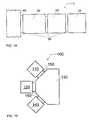
- FIGS. 1A through 1Care schematic representations of a transfer system for a drying system and a curing system according to an embodiment of the present invention
- FIG. 2is a schematic cross-sectional view of a drying system according to another embodiment of the present invention.
- FIG. 3is a schematic cross-sectional view of a curing system according to another embodiment of the present invention.
- FIG. 4is a flow chart of a method of treating a dielectric film according to yet another embodiment of the present invention.
- alternative curing methodsaddress some of the deficiencies of thermal curing. For instance, alternative curing methods are more efficient in energy transfer, as compared to thermal curing processes, and the higher energy levels found in the form of energetic particles, such as accelerated electrons, ions, or neutrals, or in the form of energetic photons, can easily excite electrons in a low-k film, thus efficiently breaking chemical bonds and dissociating side groups.
- These alternative curing methodsfacilitate the generation of cross-linking initiators (free radicals) and can improve the energy transfer required in actual cross-linking. As a result, the degree of cross-linking can be increased at a reduced thermal budget.
- ultra low-k dielectric filmsdielectric constant less than approximately 2.5
- EBelectron beam
- UVultraviolet
- IRinfrared
- MWmicrowave
- EB, UV, IR and MW curingall have their own benefits, these techniques also have limitations.
- High energy curing sourcessuch as EB and UV can provide high energy levels to generate more than enough free radicals for cross-linking, which leads to much improved mechanical properties under complementary substrate heating.
- electrons and UV photonscan cause indiscriminate dissociation of chemical bonds, which may adversely degrade the desired physical and electrical properties of the film, such as loss of hydrophobicity, increased residual film stress, collapse of pore structure, film densification and increased dielectric constant.
- low energy curing sources, such as IR and MW curingcan provide significant improvements mostly in the heat transfer efficiency, but in the meantime have side effects, such as for example skin layer or surface densification (IR), and arcing or transistor damage (MW).
- FIG. 1Ashows a processing system 1 for treating a dielectric film on a substrate, according to one embodiment of the present invention.
- the processing system 1includes a drying system 10 , and a curing system 20 coupled to the drying system 10 .
- the drying system 10can be configured to remove, or reduce to sufficient levels, one or more contaminants in the dielectric film, including, for example, moisture, solvent, porogen, or any other contaminant that may interfere with a curing process performed in the curing system 20 .
- a sufficient reduction of a specific contaminant present within the dielectric filmfrom prior to the drying process to following the drying process, can include a reduction of approximately 10% to approximately 100% of the specific contaminant.
- the level of contaminant reductionmay be measured using Fourier transform infrared (FTIR) spectroscopy, or mass spectroscopy.
- FTIRFourier transform infrared
- mass spectroscopyor mass spectroscopy.
- a sufficient reduction of a specific contaminant present within the dielectric filmcan range from approximately 50% to approximately 100%.
- a sufficient reduction of a specific contaminant present within the dielectric filmcan range from approximately 80% to approximately 100%.
- the curing system 20can be configured to cure the dielectric film by causing or partially causing cross-linking within the dielectric film in order to, for example, improve the mechanical properties of the dielectric film.
- the curing system 20can include two or more radiation sources configured to expose the substrate having the dielectric film to electromagnetic (EM) radiation at multiple EM wavelengths.
- the two or more radiation sourcescan include an infrared (IR) radiation source and an ultraviolet (UV) radiation source.
- IRinfrared
- UVultraviolet
- the exposure of the substrate to UV radiation and IR radiationcan be performed simultaneously, sequentially, or over-lapping one another. During sequential exposure, the exposure of the substrate to UV radiation can, for instance, precede the exposure of the substrate to IR radiation or vice versa.
- the IR radiationcan include an IR wave-band source ranging from approximately 1 micron to approximately 25 microns and, desirably, ranging from approximately 8 microns to approximately 14 microns.
- the UV radiationcan include a UV wave-band source producing radiation ranging from approximately 100 nanometers (nm) to approximately 600 nm and, desirably, ranging from approximately 200 nm to approximately 400 nm.
- the inventorshave recognized that the energy level (h ⁇ ) and the rate that energy is delivered to the dielectric film (q′) varies during different stages of the curing process.
- the curing processcan include mechanisms for generation of cross-link initiators, burn-out of porogens, decomposition of porogens, film cross-linking, and optionally cross-link initiator diffusion. Each mechanism may require a different energy level and rate at which energy is delivered to the dielectric film.
- cross-link initiatorsmay be generated using photon and phonon induced bond dissociation within the matrix material. Bond dissociation can require energy levels having a wavelength less than or equal to approximately 300 to 400 nm.
- porogen burn-outmay be facilitated with photon absorption by the photosensitizer.
- Porogen burn-outmay require UV wavelengths, such as wavelengths less than or equal to approximately 300 to 400 nm.
- cross-linkingcan be facilitated by thermal energy sufficient for bond formation and reorganization. Bond formation and reorganization may require energy levels having a wavelength of approximately 9 microns which, for example, corresponds to the main absorbance peak in siloxane-based organosilicate low-k materials.
- the substrate, to be treatedmay be a semiconductor, a metallic conductor, or any other substrate to which the dielectric film is to be formed upon.
- the dielectric filmcan have a dielectric constant value (before drying and/or curing, or after drying and/or curing, or both) less than the dielectric constant of SiO 2 , which is approximately 4 (e.g., the dielectric constant for thermal silicon dioxide can range from 3.8 to 3.9).
- the dielectric filmmay have a dielectric constant (before drying and/or curing, or after drying and/or curing, or both) of less than 3.0, a dielectric constant of less than 2.5, or a dielectric constant ranging from 1.6 to 2.7.
- the dielectric filmmay be described as a low-k film or an ultra low-k film.
- the dielectric filmmay, for instance, include a dual phase porous low-k film which may have a higher dielectric constant prior to porogen burn-out than following porogen burn-out. Additionally, the dielectric film may have moisture and/or other contaminants which cause the dielectric constant to be higher prior to drying and/or curing than following drying and/or curing.
- the dielectric filmcan be formed using chemical vapor deposition (CVD) techniques, or spin-on dielectric (SOD) techniques such as those offered in the Clean Track ACT 8 SOD and ACT 12 SOD coating systems commercially available from Tokyo Electron Limited (TEL).
- the Clean Track ACT 8 (200 mm) and ACT 12 (300 mm) coating systemsprovide coat, bake, and cure tools for SOD materials.
- the track systemcan be configured for processing substrate sizes of 100 mm, 200 mm, 300 mm, and greater.
- Other systems and methods for forming a dielectric film on a substrate as known to those skilled in the art of both spin-on dielectric technology and CVD dielectric technologyare suitable for the invention.
- the dielectric filmcan, for example, be characterized as a low dielectric constant (or low-k) dielectric film.
- the dielectric filmmay include at least one of an organic, inorganic, and inorganic-organic hybrid material. Additionally, the dielectric film may be porous or non-porous.
- the dielectric filmmay include an inorganic, silicate-based material, such as oxidized organosilane (or organo siloxane), deposited using CVD techniques. Examples of such films include Black DiamondTM CVD organosilicate glass (OSG) films commercially available from Applied Materials, Inc., or CoralTM CVD films commercially available from Novellus Systems.
- OSGBlack DiamondTM CVD organosilicate glass
- porous dielectric filmscan include single-phase materials, such as a silicon oxide-based matrix having terminal organic side groups that inhibit cross-linking during a curing process to create small voids (or pores).
- porous dielectric filmscan include dual-phase materials, such as a silicon oxide-based matrix having inclusions of organic material (e.g., a porogen) that is decomposed and evaporated during a curing process.
- the dielectric filmmay include an inorganic, silicate-based material, such as hydrogen silsesquioxane (HSQ) or methyl silsesquioxane (MSQ), deposited using SOD techniques.
- HSQhydrogen silsesquioxane
- MSQmethyl silsesquioxane
- the dielectric filmcan include an organic material deposited using SOD techniques.
- examples of such filmsinclude SiLK-I, SiLK-J, SiLK-H, SiLK-D, porous SiLK-T, porous SiLK-Y, and porous SiLK-Z semiconductor dielectric resins commercially available from Dow Chemical, and FLARETM, and Nano-glass commercially available from Honeywell.
- a transfer system 30can be coupled to the drying system 10 in order to transfer substrates into and out of the drying system 10 and the curing system 20 , and exchange substrates with a multi-element manufacturing system 40 .
- Transfer system 30may transfer substrates to and from drying system 10 and curing system 20 while maintaining a vacuum environment.
- the drying and curing systems 10 , 20 , and the transfer system 30can, for example, include a processing element within the multi-element manufacturing system 40 .
- the multi-element manufacturing system 40can permit the transfer of substrates to and from processing elements including such devices as etch systems, deposition systems, coating systems, patterning systems, metrology systems, etc.
- an isolation assembly 50can be utilized to couple each system.
- the isolation assembly 50can include at least one of a thermal insulation assembly to provide thermal isolation, and a gate valve assembly to provide vacuum isolation.
- the drying and curing systems 10 and 20 , and transfer system 30can be placed in any sequence.
- FIG. 1Bshows a processing system 100 for treating a dielectric film on a substrate.
- the processing system 100includes a “cluster-tool” arrangement for a drying system 110 , and a curing system 120 .
- the drying system 110can be configured to remove, or reduce to sufficient levels, one or more contaminants in the dielectric film, including, for example, moisture, solvent, porogen, or any other contaminant that may interfere with a curing process performed in the curing system 120 .
- the curing system 120can be configured to cure the dielectric film by causing or partially causing cross-linking within the dielectric film in order to, for example, improve the mechanical properties of the dielectric film.
- the processing system 100can optionally include a post-treatment system 140 configured to modify the cured dielectric film.
- post-treatmentcan include spin coating or vapor depositing another film on the dielectric film in order to promote adhesion for subsequent films or improve hydrophobicity.
- adhesion promotionmay be achieved in a post-treatment system by lightly bombarding the dielectric film with ions.
- a transfer system 130can be coupled to the drying system 110 in order to transfer substrates into and out of the drying system 110 , and can be coupled to the curing system 120 in order to transfer substrates into and out of the curing system 120 , and can be coupled to the optional post-treatment system 140 in order to transfer substrates into and out of the post-treatment system 140 .
- Transfer system 130may transfer substrates to and from drying system 110 , curing system 120 and optional post-treatment system 140 while maintaining a vacuum environment.
- transfer system 130can exchange substrates with one or more substrate cassettes (not shown). Although only two or three process systems are illustrated in FIG. 1B , other process systems can access transfer system 130 including for example such devices as etch systems, deposition systems, coating systems, patterning systems, metrology systems, etc.
- an isolation assembly 150can be utilized to couple each system.
- the isolation assembly 150can include at least one of a thermal insulation assembly to provide thermal isolation, and a gate valve assembly to provide vacuum isolation.
- the transfer system 130can serve as part of the isolation assembly 150 .
- FIG. 1Cshows a processing system 200 for treating a dielectric film on a substrate.
- the processing system 200includes a drying system 210 , and a curing system 220 .
- the drying system 210can be configured to remove, or reduce to sufficient levels, one or more contaminants in the dielectric film, including, for example, moisture, solvent, porogen, or any other contaminant that may interfere with a curing process performed in the curing system 220 .
- the curing system 220can be configured to cure the dielectric film by causing or partially causing cross-linking within the dielectric film in order to, for example, improve the mechanical properties of the dielectric film.
- the processing system 200can optionally include a post-treatment system 240 configured to modify the cured dielectric film.
- post-treatmentcan include spin coating or vapor depositing another film on the dielectric film in order to promote adhesion for subsequent films or improve hydrophobicity.
- adhesion promotionmay be achieved in a post-treatment system by lightly bombarding the dielectric film with ions.
- Drying system 210 , curing system 220 , and post-treatment system 240can be arranged horizontally or may be arranged vertically (i.e., stacked). Also, as illustrated in FIG. 1C , a transfer system 230 can be coupled to the drying system 210 in order to transfer substrates into and out of the drying system 210 , can be coupled to the curing system 220 in order to transfer substrates into and out of the curing system 220 , and can be coupled to the optional post-treatment system 240 in order to transfer substrates into and out of the post-treatment system 240 . Transfer system 230 may transfer substrates to and from drying system 210 , curing system 220 and optional post-treatment system 240 while maintaining a vacuum environment.
- transfer system 230can exchange substrates with one or more substrate cassettes (not shown). Although only three process systems are illustrated in FIG. 1C , other process systems can access transfer system 230 including for example such devices as etch systems, deposition systems, coating systems, patterning systems, metrology systems, etc.
- an isolation assembly 250can be utilized to couple each system.
- the isolation assembly 250can include at least one of a thermal insulation assembly to provide thermal isolation, and a gate valve assembly to provide vacuum isolation.
- the transfer system 230can serve as part of the isolation assembly 250 .
- At least one of the drying system 10 and the curing system 20 of the processing system 1 as depicted in FIG. 1Aincludes at least two transfer openings to permit the passage of the substrate therethrough.
- the drying system 10includes two transfer openings, the first transfer opening permits the passage of the substrate between the drying system 10 and the transfer system 30 and the second transfer opening permits the passage of the substrate between the drying system and the curing system.
- each treatment system 110 , 120 , 140 and 210 , 220 , 240respectively, includes at least one transfer opening to permit the passage of the substrate therethrough.
- Drying system 300includes a drying chamber 310 configured to produce a clean, contaminant-free environment for drying a substrate 325 resting on substrate holder 320 .
- the drying system 300can include a thermal treatment device 330 coupled to drying chamber 310 , or to substrate holder 320 , and configured to evaporate contaminants, such as for example moisture, residual solvent, etc., by elevating the temperature of substrate 325 .
- the drying system 300can include a microwave treatment device 340 coupled to the drying chamber 310 , and configured to locally heat contaminants in the presence of an oscillating electric field.
- the drying processcan utilize the thermal treatment device 330 , or the microwave treatment device 340 , or both to facilitate drying a dielectric film on substrate 325 .
- the thermal treatment device 330can include one or more conductive heating elements embedded in substrate holder 320 coupled to a power source and a temperature controller.
- each heating elementcan include a resistive heating element coupled to a power source configured to supply electrical power.
- the thermal treatment device 330can include one or more radiative heating elements coupled to a power source and a controller.
- each radiative heating elementcan include a heat lamp coupled to a power source configured to supply electrical power.
- the temperature of substrate 325can, for example, range from approximately 20° C. to approximately 500° C., and desirably, the temperature may range from approximately 200° C. to approximately 400° C.
- the microwave treatment source 340can include a variable frequency microwave source configured to sweep the microwave frequency through a bandwidth of frequencies. Frequency variation avoids charge build-up and, hence, permits damage-free application of microwave drying techniques to sensitive electronic devices.
- the drying system 300can include a drying system incorporating both a variable frequency microwave device and a thermal treatment device, such as for example the microwave furnace commercially available from Lambda Technologies, Inc. (860 Aviation Parkway, Suite 900, Morrisville, N.C. 27560).
- a microwave furnaceis described in U.S. Pat. No. 5,738,915, assigned to Lambda Technologies, Inc., and entitled “Curing polymer layers on semiconductor substrates using variable frequency microwave energy”; the entire contents of which are incorporated herein by reference.
- the substrate holder 320may or may not be configured to clamp substrate 325 .
- substrate holder 320may be configured to mechanically or electrically clamp substrate 325 .
- drying system 300can further include a gas injection system 350 coupled to the drying chamber and configured to introduce a purge gas to drying chamber 310 .
- the purge gascan, for example, include an inert gas, such as a noble gas or nitrogen.
- drying system 300can include a vacuum pumping system 355 coupled to drying chamber 310 and configured to evacuate the drying chamber 310 .
- substrate 325can be subject to an inert gas environment with or without vacuum conditions.
- drying system 300can include a controller 360 coupled to drying chamber 310 , substrate holder 320 , thermal treatment device 330 , microwave treatment device 340 , gas injection system 350 , and vacuum pumping system 355 .
- Controller 360includes a microprocessor, a memory, and a digital I/O port capable of generating control voltages sufficient to communicate and activate inputs to the drying system 300 as well as monitor outputs from the drying system 300 .
- a program stored in the memoryis utilized to interact with the drying system 300 according to a stored process recipe.
- the controller 360can be used to configure any number of processing elements ( 310 , 320 , 330 , 340 , 350 , or 355 ), and the controller 360 can collect, provide, process, store, and display data from processing elements.
- the controller 360can include a number of applications for controlling one or more of the processing elements.
- controller 360can include a graphic user interface (GUI) component (not shown) that can provide interfaces that enable a user to monitor and/or control one or more
- Curing system 400includes a curing chamber 410 configured to produce a clean, contaminant-free environment for curing a substrate 425 resting on substrate holder 420 .
- Curing system 400further includes two or more radiation sources configured to expose substrate 425 having the dielectric film to electro-magnetic (EM) radiation at multiple EM wavelengths.
- the two or more radiation sourcescan include an infrared (IR) radiation source 440 and an ultraviolet (UV) radiation source 445 .
- IR radiation source 440infrared
- UV radiation source 445ultraviolet
- the exposure of the substrate to UV radiation and IR radiationcan be performed simultaneously, sequentially, or over-lapping one another.
- the IR radiation source 440may include a broad-band IR source, or may include a narrow-band IR source.
- the IR radiation sourcecan include one or more IR lamps, or one or more IR lasers (continuous wave (CW), tunable, or pulsed), or any combination thereof.
- the IR powercan range from approximately 0.1 mW to approximately 2000 W.
- the IR radiation wavelengthcan range from approximately 1 micron to approximately 25 microns and, desirably, can range from approximately 8 microns to approximately 14 microns.
- the IR radiation source 440can include an IR element, such as a ceramic element or silicon carbide element, having a spectral output ranging from approximately 1 micron to approximately 25 microns, or the IR radiation source 440 can include a semiconductor laser (diode), or ion, Ti:sapphire, or dye laser with optical parametric amplification.
- an IR elementsuch as a ceramic element or silicon carbide element, having a spectral output ranging from approximately 1 micron to approximately 25 microns
- the IR radiation source 440can include a semiconductor laser (diode), or ion, Ti:sapphire, or dye laser with optical parametric amplification.
- the UV radiation source 445may include a broad-band UV source, or may include a narrow-band UV source.
- the UV radiation sourcecan include one or more UV lamps, or one or more UV lasers (continuous wave (CW), tunable, or pulsed), or any combination thereof.
- UV radiationcan be generated, for instance, from a microwave source, an arc discharge, a dielectric barrier discharge, or electron impact generation.
- the UV power densitycan range from approximately 0.1 mW/cm 2 to approximately 2000 mW/cm 2 .
- the UV wavelengthcan range from approximately 100 nanometers (nm) to approximately 600 nm and, desirably, can range from approximately 200 nm to approximately 400 nm.
- the UV radiation source 445can include a direct current (DC) or pulsed lamp, such as a Deuterium (D 2 ) lamp, having a spectral output ranging from approximately 180 nm to approximately 500 nm, or the UV radiation source 445 can include a semiconductor laser (diode), (nitrogen) gas laser, frequency-tripled Nd:YAG laser, or copper vapor laser.
- DCdirect current
- D 2Deuterium
- the UV radiation source 445can include a semiconductor laser (diode), (nitrogen) gas laser, frequency-tripled Nd:YAG laser, or copper vapor laser.
- the IR radiation source 440may include any number of optical device to adjust one or more properties of the output radiation.
- each sourcemay further include optical filters, optical lenses, beam expanders, beam collimators, etc.
- optical manipulation devicesas known to those skilled in the art of optics and EM wave propagation are suitable for the invention.
- the substrate holder 420can further include a temperature control system that can be configured to elevate and/or control the temperature of substrate 425 .
- the temperature control systemcan be a part of a thermal treatment device 430 .
- the substrate holder 420can include one or more conductive heating elements embedded in substrate holder 420 coupled to a power source and a temperature controller.
- each heating elementcan include a resistive heating element coupled to a power source configured to supply electrical power.
- the substrate holder 420could optionally include one or more radiative heating elements.
- the temperature of substrate 425can, for example, range from approximately 20° C. to approximately 500° C., and desirably, the temperature may range from approximately 200° C. to approximately 400° C.
- substrate holder 420may or may not be configured to clamp substrate 425 .
- substrate holder 420may be configured to mechanically or electrically clamp substrate 425 .
- curing system 400can further include a gas injection system 450 coupled to the curing chamber 410 and configured to introduce a purge gas to curing chamber 410 .
- the purge gascan, for example, include an inert gas, such as a noble gas or nitrogen.
- the purge gascan include other gases, such as for example H 2 , NH 3 , C x H y , or any combination thereof.
- curing system 400can further include a vacuum pumping system 455 coupled to curing chamber 410 and configured to evacuate the curing chamber 410 .
- substrate 425can be subject to a purge gas environment with or without vacuum conditions.
- curing system 400can include a controller 460 coupled to drying chamber 410 , substrate holder 420 , thermal treatment device 430 , IR radiation source 440 , UV radiation source 445 , gas injection system 450 , and vacuum pumping system 455 .
- Controller 460includes a microprocessor, a memory, and a digital I/O port capable of generating control voltages sufficient to communicate and activate inputs to the curing system 400 as well as monitor outputs from the curing system 400 .
- a program stored in the memoryis utilized to interact with the curing system 400 according to a stored process recipe.
- the controller 460can be used to configure any number of processing elements ( 410 , 420 , 430 , 440 , 445 , 450 , or 455 ), and the controller 460 can collect, provide, process, store, and display data from processing elements.
- the controller 460can include a number of applications for controlling one or more of the processing elements.
- controller 460can include a graphic user interface (GUI) component (not shown) that can provide easy to use interfaces that enable a user to monitor and/or control one or more processing elements.
- GUIgraphic user interface
- the controllers 360 and 460may be implemented as a DELL PRECISION WORKSTATION 610TM.
- the controllers 360 and 460may also be implemented as a general purpose computer, processor, digital signal processor, etc., which causes a substrate processing apparatus to perform a portion or all of the processing steps of the invention in response to the controllers 360 and 460 executing one or more sequences of one or more instructions contained in a computer readable medium.
- the computer readable medium or memoryfor holding instructions programmed according to the teachings of the invention and for containing data structures, tables, records, or other data described herein.
- Examples of computer readable mediaare compact discs, hard disks, floppy disks, tape, magneto-optical disks, PROMs (EPROM, EEPROM, flash EPROM), DRAM, SRAM, SDRAM, or any other magnetic medium, compact discs (e.g., CD-ROM), or any other optical medium, punch cards, paper tape, or other physical medium with patterns of holes, a carrier wave (described below), or any other medium from which a computer can read.
- the controllers 360 and 460may be locally located relative to the drying system 300 and curing system 400 , or may be remotely located relative to the drying system 300 and curing system 400 via an internet or intranet. Thus, the controllers 360 and 460 can exchange data with the drying system 300 and curing system 400 using at least one of a direct connection, an intranet, and the internet.
- the controllers 360 and 460may be coupled to an intranet at a customer site (i.e., a device maker, etc.), or coupled to an intranet at a vendor site (i.e., an equipment manufacturer).
- another computeri.e., controller, server, etc.
- controllers 360 and 460can access controllers 360 and 460 to exchange data via at least one of a direct connection, an intranet, and the internet.
- the methodincludes a flow chart 500 beginning in 510 with drying the dielectric film on the substrate in a first processing system.
- the first processing systemincludes a drying system configured to remove, or partially remove, one or more contaminants in the dielectric film, including, for example, moisture, solvent, porogen, or any other contaminant that may interfere with a subsequent curing process.
- the dielectric filmis cured in a second processing system.
- the second processing systemincludes a curing system configured to cure the dielectric film by causing or partially causing cross-linking within the dielectric film in order to, for example, improve the mechanical properties of the dielectric film.
- the substratecan be transferred from the first process system to the second processing system under vacuum in order to minimize contamination. Therein, the substrate is exposed to UV radiation and IR radiation.
- the dielectric filmmay optionally be post-treated in a post-treatment system configured to modify the cured dielectric film.
- post-treatmentcan include spin coating or vapor depositing another film on the dielectric film in order to promote adhesion for subsequent films or improve hydrophobicity.
- adhesion promotionmay be achieved in a post-treatment system by lightly bombarding the dielectric film with ions.
- a post-treatment systemby lightly bombarding the dielectric film with ions.
- One such post-treatment that can be suitable for the present inventionis described in U.S. Pat. No. 5,714,437, entitled Method of improving adhesion between thin films, the entire contents of which are incorporated herein by reference.
Landscapes
- Engineering & Computer Science (AREA)
- Physics & Mathematics (AREA)
- Microelectronics & Electronic Packaging (AREA)
- General Physics & Mathematics (AREA)
- Manufacturing & Machinery (AREA)
- Computer Hardware Design (AREA)
- Condensed Matter Physics & Semiconductors (AREA)
- Power Engineering (AREA)
- Health & Medical Sciences (AREA)
- Toxicology (AREA)
- Plasma & Fusion (AREA)
- Internal Circuitry In Semiconductor Integrated Circuit Devices (AREA)
- Formation Of Insulating Films (AREA)
- Drying Of Solid Materials (AREA)
Abstract
Description
This application is a divisional and claims the benefit of priority from U.S. application Ser. No. 11/269,581, filed Nov. 9, 2005, the entire contents of which are incorporated herein by reference.
1. Field of the Invention
The present invention relates to a multi-step system and method for treating a dielectric film and, more particularly, to an in-situ, multi-step system and method for drying and curing a dielectric film.
2. Description of Related Art
As is known to those in the semiconductor art, interconnect delay is a major limiting factor in the drive to improve the speed and performance of integrated circuits (IC). One way to minimize interconnect delay is to reduce interconnect capacitance by using low dielectric constant (low-k) materials as the insulating dielectric for metal wires in the IC devices. Thus, in recent years, low-k materials have been developed to replace relatively high dielectric constant insulating materials, such as silicon dioxide. In particular, low-k films are being utilized for inter-level and intra-level dielectric layers between metal wires in semiconductor devices. Additionally, in order to further reduce the dielectric constant of insulating materials, material films are formed with pores, i.e., porous low-k dielectric films. Such low-k films can be deposited by a spin-on dielectric (SOD) method similar to the application of photo-resist, or by chemical vapor deposition (CVD). Thus, the use of low-k materials is readily adaptable to existing semiconductor manufacturing processes.
Low-k materials are less robust than more traditional silicon dioxide, and the mechanical strength deteriorates further with the introduction of porosity. The porous low-k films can easily be damaged during plasma processing, thereby making desirable a mechanical strengthening process. It has been understood that enhancement of the material strength of porous low-k dielectrics is essential for their successful integration. Aimed at mechanical strengthening, alternative curing techniques are being explored to make porous low-k films more robust and suitable for integration.
The curing of a polymer includes a process whereby a thin film deposited for example using spin-on or vapor deposition (such as chemical vapor deposition CVD) techniques, is treated in order to cause cross-linking within the film. During the curing process, free radical polymerization is understood to be the primary route for cross-linking. As polymer chains cross-link, mechanical properties, such as for example the Young's modulus, the film hardness, the fracture toughness and the interfacial adhesion, are improved, thereby improving the fabrication robustness of the low-k film.
As there are various strategies to forming porous dielectric films with ultra low dielectric constant, the objectives of post-deposition treatments (curing) may vary from film to film, including for example the removal of moisture, the removal of solvents, the burn-out of porogens used to form the pores in the porous dielectric film, the improvement of the mechanical properties for such films, and so on.
Low dielectric constant (low k) materials are conventionally thermally cured at a temperature in the range of 300° C. to 400° C. for CVD films. For instance, furnace curing has been sufficient in producing strong, dense low-k films with a dielectric constant greater than approximately 2.5. However, when processing porous dielectric films (such as ultra low-k films) with a high level of porosity, the degree of cross-linking achievable with thermal treatment (or thermal curing) is no longer sufficient to produce films of adequate strength for a robust interconnect structure.
During thermal curing, it has been noticed that the appropriate amount of energy is delivered to the film without damaging the dielectric film. Within the temperature range of interest, however, only a small amount of free radicals can be generated. Due to the thermal energy lost in the coupling of heat to the substrate and the heat loss in the ambient environment, only a small amount of thermal energy can actually be absorbed in the low-k films to be cured. Therefore, high temperatures and long curing times are required for typical low-k furnace curing. But even with a high thermal budget, the lack of initiator generation in the thermal curing and the presence of a large amount of methyl termination in the as-deposited low-k film can make it very difficult to achieve the desired degree of cross-linking.
One aspect of the present invention permits reduction or elimination of any of the above-described problems or other problems in the prior art relating to processing dielectric films.
Another aspect of the present invention permits treatment of a dielectric film in order to cure the dielectric film.
Yet another aspect of the present invention permits treatment of a dielectric film by performing an in-situ, multi-step drying and curing process using multiple process modules coupled to one another.
Any of these and/or other aspects may be provided by a processing system for treating a dielectric film in accordance with the present invention. In one embodiment, the processing system for treating a dielectric film on a substrate includes a drying system configured to perform a drying process to reduce the amount of contaminants in or on the dielectric film and a curing system coupled to the drying system and configured to perform a curing process. The curing system includes: an ultraviolet (UV) radiation source configured to expose the dielectric film to UV radiation, and an infrared (IR) radiation source configured to expose the dielectric film to IR radiation. The system includes a transfer system coupled to the drying system and the curing system. The transfer system is configured to exchange the substrate between the drying system and the curing system under vacuum conditions.
In another embodiment, a method and computer readable medium for treating a dielectric film on a substrate includes: disposing the substrate in a drying system, drying the dielectric film according to a drying process in order to remove or partially remove contaminants on or in the dielectric film, transferring the substrate from the drying system to a curing system while maintaining vacuum conditions during the transfer, and curing the dielectric film by, exposing the dielectric film to UV radiation and exposing the dielectric film to IR radiation.
In the accompanying drawings:
In the following description, in order to facilitate a thorough understanding of the invention and for purposes of explanation and not limitation, specific details are set forth, such as a particular geometry of the processing system and descriptions of various components. However, it should be understood that the invention may be practiced in other embodiments that depart from these specific details.
The inventors recognized that alternative curing methods address some of the deficiencies of thermal curing. For instance, alternative curing methods are more efficient in energy transfer, as compared to thermal curing processes, and the higher energy levels found in the form of energetic particles, such as accelerated electrons, ions, or neutrals, or in the form of energetic photons, can easily excite electrons in a low-k film, thus efficiently breaking chemical bonds and dissociating side groups. These alternative curing methods facilitate the generation of cross-linking initiators (free radicals) and can improve the energy transfer required in actual cross-linking. As a result, the degree of cross-linking can be increased at a reduced thermal budget.
Additionally, the inventors have realized that, as film strength becomes a greater issue for the integration of ultra low-k (ULK) dielectric films (dielectric constant less than approximately 2.5), alternative curing methods can improve the mechanical properties of such films. For example, electron beam (EB), ultraviolet (UV) radiation, infrared (IR) radiation and microwave (MW) radiation may be used to cure ULK films in order to improve mechanical strength, while not sacrificing the dielectric property and film hydrophobicity.
However, although EB, UV, IR and MW curing all have their own benefits, these techniques also have limitations. High energy curing sources such as EB and UV can provide high energy levels to generate more than enough free radicals for cross-linking, which leads to much improved mechanical properties under complementary substrate heating. On the other hand, electrons and UV photons can cause indiscriminate dissociation of chemical bonds, which may adversely degrade the desired physical and electrical properties of the film, such as loss of hydrophobicity, increased residual film stress, collapse of pore structure, film densification and increased dielectric constant. Furthermore, low energy curing sources, such as IR and MW curing, can provide significant improvements mostly in the heat transfer efficiency, but in the meantime have side effects, such as for example skin layer or surface densification (IR), and arcing or transistor damage (MW).
Referring now to the drawings, wherein like reference numerals designate identical or corresponding parts throughout the several views,FIG. 1A shows aprocessing system 1 for treating a dielectric film on a substrate, according to one embodiment of the present invention. Theprocessing system 1 includes adrying system 10, and acuring system 20 coupled to thedrying system 10. For example, the dryingsystem 10 can be configured to remove, or reduce to sufficient levels, one or more contaminants in the dielectric film, including, for example, moisture, solvent, porogen, or any other contaminant that may interfere with a curing process performed in thecuring system 20.
For example, a sufficient reduction of a specific contaminant present within the dielectric film, from prior to the drying process to following the drying process, can include a reduction of approximately 10% to approximately 100% of the specific contaminant. The level of contaminant reduction may be measured using Fourier transform infrared (FTIR) spectroscopy, or mass spectroscopy. Alternatively, for example, a sufficient reduction of a specific contaminant present within the dielectric film can range from approximately 50% to approximately 100%. Alternatively, for example, a sufficient reduction of a specific contaminant present within the dielectric film can range from approximately 80% to approximately 100%.
Referring still toFIG. 1A , the curingsystem 20 can be configured to cure the dielectric film by causing or partially causing cross-linking within the dielectric film in order to, for example, improve the mechanical properties of the dielectric film. The curingsystem 20 can include two or more radiation sources configured to expose the substrate having the dielectric film to electromagnetic (EM) radiation at multiple EM wavelengths. For example, the two or more radiation sources can include an infrared (IR) radiation source and an ultraviolet (UV) radiation source. The exposure of the substrate to UV radiation and IR radiation can be performed simultaneously, sequentially, or over-lapping one another. During sequential exposure, the exposure of the substrate to UV radiation can, for instance, precede the exposure of the substrate to IR radiation or vice versa.
For example, the IR radiation can include an IR wave-band source ranging from approximately 1 micron to approximately 25 microns and, desirably, ranging from approximately 8 microns to approximately 14 microns. Additionally, for example, the UV radiation can include a UV wave-band source producing radiation ranging from approximately 100 nanometers (nm) to approximately 600 nm and, desirably, ranging from approximately 200 nm to approximately 400 nm.
The inventors have recognized that the energy level (hν) and the rate that energy is delivered to the dielectric film (q′) varies during different stages of the curing process. The curing process can include mechanisms for generation of cross-link initiators, burn-out of porogens, decomposition of porogens, film cross-linking, and optionally cross-link initiator diffusion. Each mechanism may require a different energy level and rate at which energy is delivered to the dielectric film. For instance, during the curing of the matrix material, cross-link initiators may be generated using photon and phonon induced bond dissociation within the matrix material. Bond dissociation can require energy levels having a wavelength less than or equal to approximately 300 to 400 nm. Additionally, for instance, porogen burn-out may be facilitated with photon absorption by the photosensitizer. Porogen burn-out may require UV wavelengths, such as wavelengths less than or equal to approximately 300 to 400 nm. Further yet, for instance, cross-linking can be facilitated by thermal energy sufficient for bond formation and reorganization. Bond formation and reorganization may require energy levels having a wavelength of approximately 9 microns which, for example, corresponds to the main absorbance peak in siloxane-based organosilicate low-k materials.
The substrate, to be treated, may be a semiconductor, a metallic conductor, or any other substrate to which the dielectric film is to be formed upon. The dielectric film can have a dielectric constant value (before drying and/or curing, or after drying and/or curing, or both) less than the dielectric constant of SiO2, which is approximately 4 (e.g., the dielectric constant for thermal silicon dioxide can range from 3.8 to 3.9). In various embodiments of the invention, the dielectric film may have a dielectric constant (before drying and/or curing, or after drying and/or curing, or both) of less than 3.0, a dielectric constant of less than 2.5, or a dielectric constant ranging from 1.6 to 2.7. The dielectric film may be described as a low-k film or an ultra low-k film. The dielectric film may, for instance, include a dual phase porous low-k film which may have a higher dielectric constant prior to porogen burn-out than following porogen burn-out. Additionally, the dielectric film may have moisture and/or other contaminants which cause the dielectric constant to be higher prior to drying and/or curing than following drying and/or curing.
The dielectric film can be formed using chemical vapor deposition (CVD) techniques, or spin-on dielectric (SOD) techniques such as those offered in the Clean Track ACT 8 SOD and ACT 12 SOD coating systems commercially available from Tokyo Electron Limited (TEL). The Clean Track ACT 8 (200 mm) and ACT 12 (300 mm) coating systems provide coat, bake, and cure tools for SOD materials. The track system can be configured for processing substrate sizes of 100 mm, 200 mm, 300 mm, and greater. Other systems and methods for forming a dielectric film on a substrate as known to those skilled in the art of both spin-on dielectric technology and CVD dielectric technology are suitable for the invention.
The dielectric film can, for example, be characterized as a low dielectric constant (or low-k) dielectric film. The dielectric film may include at least one of an organic, inorganic, and inorganic-organic hybrid material. Additionally, the dielectric film may be porous or non-porous. For example, the dielectric film may include an inorganic, silicate-based material, such as oxidized organosilane (or organo siloxane), deposited using CVD techniques. Examples of such films include Black Diamond™ CVD organosilicate glass (OSG) films commercially available from Applied Materials, Inc., or Coral™ CVD films commercially available from Novellus Systems. Additionally, for example, porous dielectric films can include single-phase materials, such as a silicon oxide-based matrix having terminal organic side groups that inhibit cross-linking during a curing process to create small voids (or pores). Additionally, for example, porous dielectric films can include dual-phase materials, such as a silicon oxide-based matrix having inclusions of organic material (e.g., a porogen) that is decomposed and evaporated during a curing process. Alternatively, the dielectric film may include an inorganic, silicate-based material, such as hydrogen silsesquioxane (HSQ) or methyl silsesquioxane (MSQ), deposited using SOD techniques. Examples of such films include FOx HSQ commercially available from Dow Corning, XLK porous HSQ commercially available from Dow Corning, and JSR LKD-5109 commercially available from JSR Microelectronics. Still alternatively, the dielectric film can include an organic material deposited using SOD techniques. Examples of such films include SiLK-I, SiLK-J, SiLK-H, SiLK-D, porous SiLK-T, porous SiLK-Y, and porous SiLK-Z semiconductor dielectric resins commercially available from Dow Chemical, and FLARE™, and Nano-glass commercially available from Honeywell.
Also, as illustrated inFIG. 1A , atransfer system 30 can be coupled to thedrying system 10 in order to transfer substrates into and out of the dryingsystem 10 and thecuring system 20, and exchange substrates with amulti-element manufacturing system 40.Transfer system 30 may transfer substrates to and from dryingsystem 10 and curingsystem 20 while maintaining a vacuum environment. The drying and curingsystems transfer system 30 can, for example, include a processing element within themulti-element manufacturing system 40. For example, themulti-element manufacturing system 40 can permit the transfer of substrates to and from processing elements including such devices as etch systems, deposition systems, coating systems, patterning systems, metrology systems, etc. In order to isolate the processes occurring in the first and second systems, anisolation assembly 50 can be utilized to couple each system. For instance, theisolation assembly 50 can include at least one of a thermal insulation assembly to provide thermal isolation, and a gate valve assembly to provide vacuum isolation. The drying and curingsystems transfer system 30 can be placed in any sequence.
Alternately, in another embodiment of the invention,FIG. 1B shows aprocessing system 100 for treating a dielectric film on a substrate. Theprocessing system 100 includes a “cluster-tool” arrangement for adrying system 110, and acuring system 120. For example, thedrying system 110 can be configured to remove, or reduce to sufficient levels, one or more contaminants in the dielectric film, including, for example, moisture, solvent, porogen, or any other contaminant that may interfere with a curing process performed in thecuring system 120. Additionally, for example, thecuring system 120 can be configured to cure the dielectric film by causing or partially causing cross-linking within the dielectric film in order to, for example, improve the mechanical properties of the dielectric film. Furthermore, theprocessing system 100 can optionally include apost-treatment system 140 configured to modify the cured dielectric film. For example, post-treatment can include spin coating or vapor depositing another film on the dielectric film in order to promote adhesion for subsequent films or improve hydrophobicity. Alternatively, for example, adhesion promotion may be achieved in a post-treatment system by lightly bombarding the dielectric film with ions.
Also, as illustrated inFIG. 1B , atransfer system 130 can be coupled to thedrying system 110 in order to transfer substrates into and out of thedrying system 110, and can be coupled to thecuring system 120 in order to transfer substrates into and out of thecuring system 120, and can be coupled to the optionalpost-treatment system 140 in order to transfer substrates into and out of thepost-treatment system 140.Transfer system 130 may transfer substrates to and from dryingsystem 110, curingsystem 120 and optionalpost-treatment system 140 while maintaining a vacuum environment.
Additionally,transfer system 130 can exchange substrates with one or more substrate cassettes (not shown). Although only two or three process systems are illustrated inFIG. 1B , other process systems can accesstransfer system 130 including for example such devices as etch systems, deposition systems, coating systems, patterning systems, metrology systems, etc. In order to isolate the processes occurring in the drying and curing systems, anisolation assembly 150 can be utilized to couple each system. For instance, theisolation assembly 150 can include at least one of a thermal insulation assembly to provide thermal isolation, and a gate valve assembly to provide vacuum isolation. Additionally, for example, thetransfer system 130 can serve as part of theisolation assembly 150.
Alternately, in another embodiment of the invention,FIG. 1C shows aprocessing system 200 for treating a dielectric film on a substrate. Theprocessing system 200 includes adrying system 210, and acuring system 220. For example, thedrying system 210 can be configured to remove, or reduce to sufficient levels, one or more contaminants in the dielectric film, including, for example, moisture, solvent, porogen, or any other contaminant that may interfere with a curing process performed in thecuring system 220. Additionally, for example, thecuring system 220 can be configured to cure the dielectric film by causing or partially causing cross-linking within the dielectric film in order to, for example, improve the mechanical properties of the dielectric film. Furthermore, theprocessing system 200 can optionally include apost-treatment system 240 configured to modify the cured dielectric film. For example, post-treatment can include spin coating or vapor depositing another film on the dielectric film in order to promote adhesion for subsequent films or improve hydrophobicity. Alternatively, for example, adhesion promotion may be achieved in a post-treatment system by lightly bombarding the dielectric film with ions.
Additionally,transfer system 230 can exchange substrates with one or more substrate cassettes (not shown). Although only three process systems are illustrated inFIG. 1C , other process systems can accesstransfer system 230 including for example such devices as etch systems, deposition systems, coating systems, patterning systems, metrology systems, etc. In order to isolate the processes occurring in the first and second systems, anisolation assembly 250 can be utilized to couple each system. For instance, theisolation assembly 250 can include at least one of a thermal insulation assembly to provide thermal isolation, and a gate valve assembly to provide vacuum isolation. Additionally, for example, thetransfer system 230 can serve as part of theisolation assembly 250.
At least one of the dryingsystem 10 and thecuring system 20 of theprocessing system 1 as depicted inFIG. 1A includes at least two transfer openings to permit the passage of the substrate therethrough. For example, as depicted inFIG. 1A , the dryingsystem 10 includes two transfer openings, the first transfer opening permits the passage of the substrate between the dryingsystem 10 and thetransfer system 30 and the second transfer opening permits the passage of the substrate between the drying system and the curing system. However, regarding theprocessing system 100 depicted inFIG. 1B and theprocessing system 200 depicted inFIG. 1C , eachtreatment system
Referring now toFIG. 2 , adrying system 300 is shown according to another embodiment of the invention.Drying system 300 includes a dryingchamber 310 configured to produce a clean, contaminant-free environment for drying asubstrate 325 resting onsubstrate holder 320. Thedrying system 300 can include athermal treatment device 330 coupled to dryingchamber 310, or tosubstrate holder 320, and configured to evaporate contaminants, such as for example moisture, residual solvent, etc., by elevating the temperature ofsubstrate 325. Furthermore, thedrying system 300 can include amicrowave treatment device 340 coupled to the dryingchamber 310, and configured to locally heat contaminants in the presence of an oscillating electric field. The drying process can utilize thethermal treatment device 330, or themicrowave treatment device 340, or both to facilitate drying a dielectric film onsubstrate 325.
Thethermal treatment device 330 can include one or more conductive heating elements embedded insubstrate holder 320 coupled to a power source and a temperature controller. For example, each heating element can include a resistive heating element coupled to a power source configured to supply electrical power. Alternatively, thethermal treatment device 330 can include one or more radiative heating elements coupled to a power source and a controller. For example, each radiative heating element can include a heat lamp coupled to a power source configured to supply electrical power. The temperature ofsubstrate 325 can, for example, range from approximately 20° C. to approximately 500° C., and desirably, the temperature may range from approximately 200° C. to approximately 400° C.
Themicrowave treatment source 340 can include a variable frequency microwave source configured to sweep the microwave frequency through a bandwidth of frequencies. Frequency variation avoids charge build-up and, hence, permits damage-free application of microwave drying techniques to sensitive electronic devices.
In one example, thedrying system 300 can include a drying system incorporating both a variable frequency microwave device and a thermal treatment device, such as for example the microwave furnace commercially available from Lambda Technologies, Inc. (860 Aviation Parkway, Suite 900, Morrisville, N.C. 27560). For additional details, a microwave furnace is described in U.S. Pat. No. 5,738,915, assigned to Lambda Technologies, Inc., and entitled “Curing polymer layers on semiconductor substrates using variable frequency microwave energy”; the entire contents of which are incorporated herein by reference.
Thesubstrate holder 320 may or may not be configured to clampsubstrate 325. For instance,substrate holder 320 may be configured to mechanically orelectrically clamp substrate 325.
Referring again toFIG. 2 , dryingsystem 300 can further include agas injection system 350 coupled to the drying chamber and configured to introduce a purge gas to dryingchamber 310. The purge gas can, for example, include an inert gas, such as a noble gas or nitrogen. Additionally, dryingsystem 300 can include avacuum pumping system 355 coupled to dryingchamber 310 and configured to evacuate the dryingchamber 310. During a drying process,substrate 325 can be subject to an inert gas environment with or without vacuum conditions.
Furthermore, dryingsystem 300 can include acontroller 360 coupled to dryingchamber 310,substrate holder 320,thermal treatment device 330,microwave treatment device 340,gas injection system 350, andvacuum pumping system 355.Controller 360 includes a microprocessor, a memory, and a digital I/O port capable of generating control voltages sufficient to communicate and activate inputs to thedrying system 300 as well as monitor outputs from thedrying system 300. A program stored in the memory is utilized to interact with thedrying system 300 according to a stored process recipe. Thecontroller 360 can be used to configure any number of processing elements (310,320,330,340,350, or355), and thecontroller 360 can collect, provide, process, store, and display data from processing elements. Thecontroller 360 can include a number of applications for controlling one or more of the processing elements. For example,controller 360 can include a graphic user interface (GUI) component (not shown) that can provide interfaces that enable a user to monitor and/or control one or more processing elements.
Referring now toFIG. 3 , acuring system 400 is shown according to another embodiment of the present invention.Curing system 400 includes a curingchamber 410 configured to produce a clean, contaminant-free environment for curing asubstrate 425 resting onsubstrate holder 420.Curing system 400 further includes two or more radiation sources configured to exposesubstrate 425 having the dielectric film to electro-magnetic (EM) radiation at multiple EM wavelengths. The two or more radiation sources can include an infrared (IR)radiation source 440 and an ultraviolet (UV)radiation source 445. The exposure of the substrate to UV radiation and IR radiation can be performed simultaneously, sequentially, or over-lapping one another.
TheIR radiation source 440 may include a broad-band IR source, or may include a narrow-band IR source. The IR radiation source can include one or more IR lamps, or one or more IR lasers (continuous wave (CW), tunable, or pulsed), or any combination thereof. The IR power can range from approximately 0.1 mW to approximately 2000 W. The IR radiation wavelength can range from approximately 1 micron to approximately 25 microns and, desirably, can range from approximately 8 microns to approximately 14 microns. For example, theIR radiation source 440 can include an IR element, such as a ceramic element or silicon carbide element, having a spectral output ranging from approximately 1 micron to approximately 25 microns, or theIR radiation source 440 can include a semiconductor laser (diode), or ion, Ti:sapphire, or dye laser with optical parametric amplification.
TheUV radiation source 445 may include a broad-band UV source, or may include a narrow-band UV source. The UV radiation source can include one or more UV lamps, or one or more UV lasers (continuous wave (CW), tunable, or pulsed), or any combination thereof. UV radiation can be generated, for instance, from a microwave source, an arc discharge, a dielectric barrier discharge, or electron impact generation. The UV power density can range from approximately 0.1 mW/cm2to approximately 2000 mW/cm2. The UV wavelength can range from approximately 100 nanometers (nm) to approximately 600 nm and, desirably, can range from approximately 200 nm to approximately 400 nm. For example, theUV radiation source 445 can include a direct current (DC) or pulsed lamp, such as a Deuterium (D2) lamp, having a spectral output ranging from approximately 180 nm to approximately 500 nm, or theUV radiation source 445 can include a semiconductor laser (diode), (nitrogen) gas laser, frequency-tripled Nd:YAG laser, or copper vapor laser.
TheIR radiation source 440, or theUV radiation source 445, or both, may include any number of optical device to adjust one or more properties of the output radiation. For example, each source may further include optical filters, optical lenses, beam expanders, beam collimators, etc. Such optical manipulation devices as known to those skilled in the art of optics and EM wave propagation are suitable for the invention.
Thesubstrate holder 420 can further include a temperature control system that can be configured to elevate and/or control the temperature ofsubstrate 425. The temperature control system can be a part of athermal treatment device 430. Thesubstrate holder 420 can include one or more conductive heating elements embedded insubstrate holder 420 coupled to a power source and a temperature controller. For example, each heating element can include a resistive heating element coupled to a power source configured to supply electrical power. Thesubstrate holder 420 could optionally include one or more radiative heating elements. The temperature ofsubstrate 425 can, for example, range from approximately 20° C. to approximately 500° C., and desirably, the temperature may range from approximately 200° C. to approximately 400° C.
Additionally, thesubstrate holder 420 may or may not be configured to clampsubstrate 425. For instance,substrate holder 420 may be configured to mechanically orelectrically clamp substrate 425.
Referring again toFIG. 3 ,curing system 400 can further include agas injection system 450 coupled to thecuring chamber 410 and configured to introduce a purge gas to curingchamber 410. The purge gas can, for example, include an inert gas, such as a noble gas or nitrogen. Alternatively, the purge gas can include other gases, such as for example H2, NH3, CxHy, or any combination thereof. Additionally, curingsystem 400 can further include avacuum pumping system 455 coupled to curingchamber 410 and configured to evacuate thecuring chamber 410. During a curing process,substrate 425 can be subject to a purge gas environment with or without vacuum conditions.
Furthermore, curingsystem 400 can include acontroller 460 coupled to dryingchamber 410,substrate holder 420,thermal treatment device 430,IR radiation source 440,UV radiation source 445,gas injection system 450, andvacuum pumping system 455.Controller 460 includes a microprocessor, a memory, and a digital I/O port capable of generating control voltages sufficient to communicate and activate inputs to thecuring system 400 as well as monitor outputs from thecuring system 400. A program stored in the memory is utilized to interact with thecuring system 400 according to a stored process recipe. Thecontroller 460 can be used to configure any number of processing elements (410,420,430,440,445,450, or455), and thecontroller 460 can collect, provide, process, store, and display data from processing elements. Thecontroller 460 can include a number of applications for controlling one or more of the processing elements. For example,controller 460 can include a graphic user interface (GUI) component (not shown) that can provide easy to use interfaces that enable a user to monitor and/or control one or more processing elements.
Thecontrollers controllers controllers
Thecontrollers drying system 300 and curingsystem 400, or may be remotely located relative to thedrying system 300 and curingsystem 400 via an internet or intranet. Thus, thecontrollers drying system 300 and curingsystem 400 using at least one of a direct connection, an intranet, and the internet. Thecontrollers controllers
Referring now toFIG. 4 , a method of treating a dielectric film on a substrate is described according to another embodiment. The method includes aflow chart 500 beginning in510 with drying the dielectric film on the substrate in a first processing system. The first processing system includes a drying system configured to remove, or partially remove, one or more contaminants in the dielectric film, including, for example, moisture, solvent, porogen, or any other contaminant that may interfere with a subsequent curing process.
In520, the dielectric film is cured in a second processing system. The second processing system includes a curing system configured to cure the dielectric film by causing or partially causing cross-linking within the dielectric film in order to, for example, improve the mechanical properties of the dielectric film. Following the drying process, the substrate can be transferred from the first process system to the second processing system under vacuum in order to minimize contamination. Therein, the substrate is exposed to UV radiation and IR radiation. Additionally, following the drying and curing processes, the dielectric film may optionally be post-treated in a post-treatment system configured to modify the cured dielectric film. For example, post-treatment can include spin coating or vapor depositing another film on the dielectric film in order to promote adhesion for subsequent films or improve hydrophobicity. Alternatively, for example, adhesion promotion may be achieved in a post-treatment system by lightly bombarding the dielectric film with ions. One such post-treatment that can be suitable for the present invention is described in U.S. Pat. No. 5,714,437, entitled Method of improving adhesion between thin films, the entire contents of which are incorporated herein by reference.
Although only certain exemplary embodiments of this invention have been described in detail above, those skilled in the art will readily appreciate that many modifications are possible in the exemplary embodiments without materially departing from the novel teachings and advantages of this invention. Accordingly, all such modifications are intended to be included within the scope of this invention.
Claims (18)
1. A method of treating a dielectric film on a substrate, comprising:
disposing said substrate in a curing system; and
curing said dielectric film by:
exposing said dielectric film to infrared (IR) radiation ranging from approximately 8 microns to approximately 14 microns to facilitate cross-linking by thermal energy sufficient for bond formation and reorganization during one stage of said curing, and
exposing said dielectric film to ultraviolet (UV) radiation ranging from approximately 100nm to approximately 600nm to also perform at least one of generating cross-link initiators by bond dissociation and facilitating porogen burn out during another stage of said curing said dielectric film, wherein at least part of said exposing to IR radiation and said exposing to UV radiation is performed simultaneously.
2. The method ofclaim 1 , wherein said exposing said dielectric film to UV radiation comprises:
exposing said dielectric film to UV radiation from one or more UV lamps, or one or more UV lasers, or both of one or more UV lamps and the one or more UV lasers;
exposing said dielectric film to said UV radiation at an energy level sufficient to generate said cross-link initiators using photon and photon-induced bond dissociation within a matrix material of said dielectric film; and
exposing said dielectric film to said UV radiation at an energy level sufficient to facilitate said porogen burn-out with photon absorption.
3. The method ofclaim 1 , wherein said exposing said dielectric film to IR radiation comprises:
exposing said dielectric film to IR radiation from one or more IR lamps, or one or more IR lasers, or both of the one or more IR lamps and the one or more IR lasers; and
exposing said dielectric film to said IR radiation at an energy level which corresponds to a main absorption peak of the dielectric film.
4. The method ofclaim 1 , further comprising:
treating said dielectric film following said curing by performing one or more of depositing another film on said dielectric film, cleaning said dielectric film, or exposing said dielectric film to a plasma.
5. The method ofclaim 1 , wherein said curing comprises treating a low-k dielectric film.
6. The method ofclaim 1 , wherein said exposing said dielectric film to IR radiation and said exposing said dielectric film to UV radiation are performed simultaneously.
7. The method ofclaim 1 , wherein said exposing said dielectric film to IR radiation and said exposing said dielectric film to UV radiation are performed sequentially.
8. The method ofclaim 1 , wherein said exposing said dielectric film to IR radiation and said exposing said dielectric film to UV radiation are performed overlapping one another.
9. The method ofclaim 1 , wherein said exposing said dielectric film to UV radiation comprises a UV wavelength ranging from about 200 nm to about 400 nm.
10. The method ofclaim 1 , further comprising heating said substrate.
11. The method ofclaim 10 , wherein said heating comprises elevating said substrate to a temperature ranging from about 20 degrees C. to about 500 degrees C.
12. The method ofclaim 11 , wherein said heating comprises elevating said substrate to a temperature ranging from about 200 degrees C. to about 400 degrees C.
13. The method ofclaim 10 , wherein said heating is performed during said exposing said dielectric film to UV radiation.
14. The method ofclaim 10 , wherein said heating is performed during said exposing said dielectric film to IR radiation.
15. The method ofclaim 10 , further comprising controlling a temperature of said substrate.
16. The method ofclaim 15 , further comprising clamping said substrate to a substrate holder during said controlling.
17. The method ofclaim 1 , wherein said dielectric film comprises a porous low dielectric constant (low-k) film.
18. The method ofclaim 1 , further comprising
disposing said substrate in a drying system;
drying said dielectric film according to a drying process in order to remove or partially remove undesired residues or absorbates on or in said dielectric film;
transferring said substrate from said drying system to said curing system while maintaining vacuum conditions during said transfer.
Priority Applications (4)
| Application Number | Priority Date | Filing Date | Title |
|---|---|---|---|
| US12/605,863US8642488B2 (en) | 2005-11-09 | 2009-10-26 | Multi-step system and method for curing a dielectric film |
| US14/142,340US9184047B2 (en) | 2005-11-09 | 2013-12-27 | Multi-step system and method for curing a dielectric film |
| US14/877,136US9443725B2 (en) | 2005-11-09 | 2015-10-07 | Multi-step system and method for curing a dielectric film |
| US15/204,279US10068765B2 (en) | 2005-11-09 | 2016-07-07 | Multi-step system and method for curing a dielectric film |
Applications Claiming Priority (2)
| Application Number | Priority Date | Filing Date | Title |
|---|---|---|---|
| US11/269,581US7622378B2 (en) | 2005-11-09 | 2005-11-09 | Multi-step system and method for curing a dielectric film |
| US12/605,863US8642488B2 (en) | 2005-11-09 | 2009-10-26 | Multi-step system and method for curing a dielectric film |
Related Parent Applications (1)
| Application Number | Title | Priority Date | Filing Date |
|---|---|---|---|
| US11/269,581DivisionUS7622378B2 (en) | 2005-11-09 | 2005-11-09 | Multi-step system and method for curing a dielectric film |
Related Child Applications (1)
| Application Number | Title | Priority Date | Filing Date |
|---|---|---|---|
| US14/142,340ContinuationUS9184047B2 (en) | 2005-11-09 | 2013-12-27 | Multi-step system and method for curing a dielectric film |
Publications (2)
| Publication Number | Publication Date |
|---|---|
| US20100041248A1 US20100041248A1 (en) | 2010-02-18 |
| US8642488B2true US8642488B2 (en) | 2014-02-04 |
Family
ID=38004345
Family Applications (5)
| Application Number | Title | Priority Date | Filing Date |
|---|---|---|---|
| US11/269,581Active2026-08-24US7622378B2 (en) | 2005-11-09 | 2005-11-09 | Multi-step system and method for curing a dielectric film |
| US12/605,863Expired - Fee RelatedUS8642488B2 (en) | 2005-11-09 | 2009-10-26 | Multi-step system and method for curing a dielectric film |
| US14/142,340Expired - Fee RelatedUS9184047B2 (en) | 2005-11-09 | 2013-12-27 | Multi-step system and method for curing a dielectric film |
| US14/877,136Expired - Fee RelatedUS9443725B2 (en) | 2005-11-09 | 2015-10-07 | Multi-step system and method for curing a dielectric film |
| US15/204,279Expired - Fee RelatedUS10068765B2 (en) | 2005-11-09 | 2016-07-07 | Multi-step system and method for curing a dielectric film |
Family Applications Before (1)
| Application Number | Title | Priority Date | Filing Date |
|---|---|---|---|
| US11/269,581Active2026-08-24US7622378B2 (en) | 2005-11-09 | 2005-11-09 | Multi-step system and method for curing a dielectric film |
Family Applications After (3)
| Application Number | Title | Priority Date | Filing Date |
|---|---|---|---|
| US14/142,340Expired - Fee RelatedUS9184047B2 (en) | 2005-11-09 | 2013-12-27 | Multi-step system and method for curing a dielectric film |
| US14/877,136Expired - Fee RelatedUS9443725B2 (en) | 2005-11-09 | 2015-10-07 | Multi-step system and method for curing a dielectric film |
| US15/204,279Expired - Fee RelatedUS10068765B2 (en) | 2005-11-09 | 2016-07-07 | Multi-step system and method for curing a dielectric film |
Country Status (6)
| Country | Link |
|---|---|
| US (5) | US7622378B2 (en) |
| JP (1) | JP5496512B2 (en) |
| KR (1) | KR101291017B1 (en) |
| CN (2) | CN101517708A (en) |
| TW (1) | TWI360832B (en) |
| WO (1) | WO2007055849A2 (en) |
Cited By (354)
| Publication number | Priority date | Publication date | Assignee | Title |
|---|---|---|---|---|
| US9443725B2 (en)* | 2005-11-09 | 2016-09-13 | Tokyo Electron Limited | Multi-step system and method for curing a dielectric film |
| US9576848B2 (en) | 2014-11-25 | 2017-02-21 | Samsung Electronics Co., Ltd. | Method of treating a porous dielectric layer and a method of fabricating a semiconductor device using the same |
| US10083836B2 (en) | 2015-07-24 | 2018-09-25 | Asm Ip Holding B.V. | Formation of boron-doped titanium metal films with high work function |
| US10103040B1 (en) | 2017-03-31 | 2018-10-16 | Asm Ip Holding B.V. | Apparatus and method for manufacturing a semiconductor device |
| US10134757B2 (en) | 2016-11-07 | 2018-11-20 | Asm Ip Holding B.V. | Method of processing a substrate and a device manufactured by using the method |
| US10229833B2 (en) | 2016-11-01 | 2019-03-12 | Asm Ip Holding B.V. | Methods for forming a transition metal nitride film on a substrate by atomic layer deposition and related semiconductor device structures |
| US10249524B2 (en) | 2017-08-09 | 2019-04-02 | Asm Ip Holding B.V. | Cassette holder assembly for a substrate cassette and holding member for use in such assembly |
| US10249577B2 (en) | 2016-05-17 | 2019-04-02 | Asm Ip Holding B.V. | Method of forming metal interconnection and method of fabricating semiconductor apparatus using the method |
| US10262859B2 (en) | 2016-03-24 | 2019-04-16 | Asm Ip Holding B.V. | Process for forming a film on a substrate using multi-port injection assemblies |
| US10269558B2 (en) | 2016-12-22 | 2019-04-23 | Asm Ip Holding B.V. | Method of forming a structure on a substrate |
| US10276355B2 (en) | 2015-03-12 | 2019-04-30 | Asm Ip Holding B.V. | Multi-zone reactor, system including the reactor, and method of using the same |
| US10283353B2 (en) | 2017-03-29 | 2019-05-07 | Asm Ip Holding B.V. | Method of reforming insulating film deposited on substrate with recess pattern |
| US10290508B1 (en) | 2017-12-05 | 2019-05-14 | Asm Ip Holding B.V. | Method for forming vertical spacers for spacer-defined patterning |
| US10312129B2 (en) | 2015-09-29 | 2019-06-04 | Asm Ip Holding B.V. | Variable adjustment for precise matching of multiple chamber cavity housings |
| US10312055B2 (en) | 2017-07-26 | 2019-06-04 | Asm Ip Holding B.V. | Method of depositing film by PEALD using negative bias |
| US10319588B2 (en) | 2017-10-10 | 2019-06-11 | Asm Ip Holding B.V. | Method for depositing a metal chalcogenide on a substrate by cyclical deposition |
| US10322384B2 (en) | 2015-11-09 | 2019-06-18 | Asm Ip Holding B.V. | Counter flow mixer for process chamber |
| US10340125B2 (en) | 2013-03-08 | 2019-07-02 | Asm Ip Holding B.V. | Pulsed remote plasma method and system |
| US10340135B2 (en) | 2016-11-28 | 2019-07-02 | Asm Ip Holding B.V. | Method of topologically restricted plasma-enhanced cyclic deposition of silicon or metal nitride |
| US10343920B2 (en) | 2016-03-18 | 2019-07-09 | Asm Ip Holding B.V. | Aligned carbon nanotubes |
| US10361201B2 (en) | 2013-09-27 | 2019-07-23 | Asm Ip Holding B.V. | Semiconductor structure and device formed using selective epitaxial process |
| US10366864B2 (en) | 2013-03-08 | 2019-07-30 | Asm Ip Holding B.V. | Method and system for in-situ formation of intermediate reactive species |
| US10364496B2 (en) | 2011-06-27 | 2019-07-30 | Asm Ip Holding B.V. | Dual section module having shared and unshared mass flow controllers |
| US10367080B2 (en) | 2016-05-02 | 2019-07-30 | Asm Ip Holding B.V. | Method of forming a germanium oxynitride film |
| US10381226B2 (en) | 2016-07-27 | 2019-08-13 | Asm Ip Holding B.V. | Method of processing substrate |
| US10378106B2 (en) | 2008-11-14 | 2019-08-13 | Asm Ip Holding B.V. | Method of forming insulation film by modified PEALD |
| US10381219B1 (en) | 2018-10-25 | 2019-08-13 | Asm Ip Holding B.V. | Methods for forming a silicon nitride film |
| US10388509B2 (en) | 2016-06-28 | 2019-08-20 | Asm Ip Holding B.V. | Formation of epitaxial layers via dislocation filtering |
| US10388513B1 (en) | 2018-07-03 | 2019-08-20 | Asm Ip Holding B.V. | Method for depositing silicon-free carbon-containing film as gap-fill layer by pulse plasma-assisted deposition |
| US10395919B2 (en) | 2016-07-28 | 2019-08-27 | Asm Ip Holding B.V. | Method and apparatus for filling a gap |
| US10403504B2 (en) | 2017-10-05 | 2019-09-03 | Asm Ip Holding B.V. | Method for selectively depositing a metallic film on a substrate |
| US10410943B2 (en) | 2016-10-13 | 2019-09-10 | Asm Ip Holding B.V. | Method for passivating a surface of a semiconductor and related systems |
| US10435790B2 (en) | 2016-11-01 | 2019-10-08 | Asm Ip Holding B.V. | Method of subatmospheric plasma-enhanced ALD using capacitively coupled electrodes with narrow gap |
| US10438965B2 (en) | 2014-12-22 | 2019-10-08 | Asm Ip Holding B.V. | Semiconductor device and manufacturing method thereof |
| US10446393B2 (en) | 2017-05-08 | 2019-10-15 | Asm Ip Holding B.V. | Methods for forming silicon-containing epitaxial layers and related semiconductor device structures |
| US10458018B2 (en) | 2015-06-26 | 2019-10-29 | Asm Ip Holding B.V. | Structures including metal carbide material, devices including the structures, and methods of forming same |
| US10468261B2 (en) | 2017-02-15 | 2019-11-05 | Asm Ip Holding B.V. | Methods for forming a metallic film on a substrate by cyclical deposition and related semiconductor device structures |
| US10468251B2 (en) | 2016-02-19 | 2019-11-05 | Asm Ip Holding B.V. | Method for forming spacers using silicon nitride film for spacer-defined multiple patterning |
| US10480072B2 (en) | 2009-04-06 | 2019-11-19 | Asm Ip Holding B.V. | Semiconductor processing reactor and components thereof |
| US10483099B1 (en) | 2018-07-26 | 2019-11-19 | Asm Ip Holding B.V. | Method for forming thermally stable organosilicon polymer film |
| US10501866B2 (en) | 2016-03-09 | 2019-12-10 | Asm Ip Holding B.V. | Gas distribution apparatus for improved film uniformity in an epitaxial system |
| US10504742B2 (en) | 2017-05-31 | 2019-12-10 | Asm Ip Holding B.V. | Method of atomic layer etching using hydrogen plasma |
| US10510536B2 (en) | 2018-03-29 | 2019-12-17 | Asm Ip Holding B.V. | Method of depositing a co-doped polysilicon film on a surface of a substrate within a reaction chamber |
| US10529554B2 (en) | 2016-02-19 | 2020-01-07 | Asm Ip Holding B.V. | Method for forming silicon nitride film selectively on sidewalls or flat surfaces of trenches |
| US10529542B2 (en) | 2015-03-11 | 2020-01-07 | Asm Ip Holdings B.V. | Cross-flow reactor and method |
| US10529563B2 (en) | 2017-03-29 | 2020-01-07 | Asm Ip Holdings B.V. | Method for forming doped metal oxide films on a substrate by cyclical deposition and related semiconductor device structures |
| US10535516B2 (en) | 2018-02-01 | 2020-01-14 | Asm Ip Holdings B.V. | Method for depositing a semiconductor structure on a surface of a substrate and related semiconductor structures |
| US10541333B2 (en) | 2017-07-19 | 2020-01-21 | Asm Ip Holding B.V. | Method for depositing a group IV semiconductor and related semiconductor device structures |
| US10541173B2 (en) | 2016-07-08 | 2020-01-21 | Asm Ip Holding B.V. | Selective deposition method to form air gaps |
| US10559458B1 (en) | 2018-11-26 | 2020-02-11 | Asm Ip Holding B.V. | Method of forming oxynitride film |
| US10561975B2 (en) | 2014-10-07 | 2020-02-18 | Asm Ip Holdings B.V. | Variable conductance gas distribution apparatus and method |
| US10566223B2 (en) | 2012-08-28 | 2020-02-18 | Asm Ip Holdings B.V. | Systems and methods for dynamic semiconductor process scheduling |
| US10590535B2 (en) | 2017-07-26 | 2020-03-17 | Asm Ip Holdings B.V. | Chemical treatment, deposition and/or infiltration apparatus and method for using the same |
| US10600673B2 (en) | 2015-07-07 | 2020-03-24 | Asm Ip Holding B.V. | Magnetic susceptor to baseplate seal |
| US10605530B2 (en) | 2017-07-26 | 2020-03-31 | Asm Ip Holding B.V. | Assembly of a liner and a flange for a vertical furnace as well as the liner and the vertical furnace |
| US10607895B2 (en) | 2017-09-18 | 2020-03-31 | Asm Ip Holdings B.V. | Method for forming a semiconductor device structure comprising a gate fill metal |
| US10604847B2 (en) | 2014-03-18 | 2020-03-31 | Asm Ip Holding B.V. | Gas distribution system, reactor including the system, and methods of using the same |
| USD880437S1 (en) | 2018-02-01 | 2020-04-07 | Asm Ip Holding B.V. | Gas supply plate for semiconductor manufacturing apparatus |
| US10612136B2 (en) | 2018-06-29 | 2020-04-07 | ASM IP Holding, B.V. | Temperature-controlled flange and reactor system including same |
| US10612137B2 (en) | 2016-07-08 | 2020-04-07 | Asm Ip Holdings B.V. | Organic reactants for atomic layer deposition |
| US10643904B2 (en) | 2016-11-01 | 2020-05-05 | Asm Ip Holdings B.V. | Methods for forming a semiconductor device and related semiconductor device structures |
| US10643826B2 (en) | 2016-10-26 | 2020-05-05 | Asm Ip Holdings B.V. | Methods for thermally calibrating reaction chambers |
| US10658205B2 (en) | 2017-09-28 | 2020-05-19 | Asm Ip Holdings B.V. | Chemical dispensing apparatus and methods for dispensing a chemical to a reaction chamber |
| US10655221B2 (en) | 2017-02-09 | 2020-05-19 | Asm Ip Holding B.V. | Method for depositing oxide film by thermal ALD and PEALD |
| US10658181B2 (en) | 2018-02-20 | 2020-05-19 | Asm Ip Holding B.V. | Method of spacer-defined direct patterning in semiconductor fabrication |
| US10665452B2 (en) | 2016-05-02 | 2020-05-26 | Asm Ip Holdings B.V. | Source/drain performance through conformal solid state doping |
| US10683571B2 (en) | 2014-02-25 | 2020-06-16 | Asm Ip Holding B.V. | Gas supply manifold and method of supplying gases to chamber using same |
| US10685834B2 (en) | 2017-07-05 | 2020-06-16 | Asm Ip Holdings B.V. | Methods for forming a silicon germanium tin layer and related semiconductor device structures |
| US10692741B2 (en) | 2017-08-08 | 2020-06-23 | Asm Ip Holdings B.V. | Radiation shield |
| US10707106B2 (en) | 2011-06-06 | 2020-07-07 | Asm Ip Holding B.V. | High-throughput semiconductor-processing apparatus equipped with multiple dual-chamber modules |
| US10714385B2 (en) | 2016-07-19 | 2020-07-14 | Asm Ip Holding B.V. | Selective deposition of tungsten |
| US10714315B2 (en) | 2012-10-12 | 2020-07-14 | Asm Ip Holdings B.V. | Semiconductor reaction chamber showerhead |
| US10714335B2 (en) | 2017-04-25 | 2020-07-14 | Asm Ip Holding B.V. | Method of depositing thin film and method of manufacturing semiconductor device |
| US10714350B2 (en) | 2016-11-01 | 2020-07-14 | ASM IP Holdings, B.V. | Methods for forming a transition metal niobium nitride film on a substrate by atomic layer deposition and related semiconductor device structures |
| US10731249B2 (en) | 2018-02-15 | 2020-08-04 | Asm Ip Holding B.V. | Method of forming a transition metal containing film on a substrate by a cyclical deposition process, a method for supplying a transition metal halide compound to a reaction chamber, and related vapor deposition apparatus |
| US10734244B2 (en) | 2017-11-16 | 2020-08-04 | Asm Ip Holding B.V. | Method of processing a substrate and a device manufactured by the same |
| US10734497B2 (en) | 2017-07-18 | 2020-08-04 | Asm Ip Holding B.V. | Methods for forming a semiconductor device structure and related semiconductor device structures |
| US10741385B2 (en) | 2016-07-28 | 2020-08-11 | Asm Ip Holding B.V. | Method and apparatus for filling a gap |
| US10755922B2 (en) | 2018-07-03 | 2020-08-25 | Asm Ip Holding B.V. | Method for depositing silicon-free carbon-containing film as gap-fill layer by pulse plasma-assisted deposition |
| US10767789B2 (en) | 2018-07-16 | 2020-09-08 | Asm Ip Holding B.V. | Diaphragm valves, valve components, and methods for forming valve components |
| US10770286B2 (en) | 2017-05-08 | 2020-09-08 | Asm Ip Holdings B.V. | Methods for selectively forming a silicon nitride film on a substrate and related semiconductor device structures |
| US10770336B2 (en) | 2017-08-08 | 2020-09-08 | Asm Ip Holding B.V. | Substrate lift mechanism and reactor including same |
| US10787741B2 (en) | 2014-08-21 | 2020-09-29 | Asm Ip Holding B.V. | Method and system for in situ formation of gas-phase compounds |
| US10797133B2 (en) | 2018-06-21 | 2020-10-06 | Asm Ip Holding B.V. | Method for depositing a phosphorus doped silicon arsenide film and related semiconductor device structures |
| US10804098B2 (en) | 2009-08-14 | 2020-10-13 | Asm Ip Holding B.V. | Systems and methods for thin-film deposition of metal oxides using excited nitrogen-oxygen species |
| US10811256B2 (en) | 2018-10-16 | 2020-10-20 | Asm Ip Holding B.V. | Method for etching a carbon-containing feature |
| USD900036S1 (en) | 2017-08-24 | 2020-10-27 | Asm Ip Holding B.V. | Heater electrical connector and adapter |
| US10818758B2 (en) | 2018-11-16 | 2020-10-27 | Asm Ip Holding B.V. | Methods for forming a metal silicate film on a substrate in a reaction chamber and related semiconductor device structures |
| US10832903B2 (en) | 2011-10-28 | 2020-11-10 | Asm Ip Holding B.V. | Process feed management for semiconductor substrate processing |
| US10829852B2 (en) | 2018-08-16 | 2020-11-10 | Asm Ip Holding B.V. | Gas distribution device for a wafer processing apparatus |
| US10844484B2 (en) | 2017-09-22 | 2020-11-24 | Asm Ip Holding B.V. | Apparatus for dispensing a vapor phase reactant to a reaction chamber and related methods |
| US10847366B2 (en) | 2018-11-16 | 2020-11-24 | Asm Ip Holding B.V. | Methods for depositing a transition metal chalcogenide film on a substrate by a cyclical deposition process |
| US10847371B2 (en) | 2018-03-27 | 2020-11-24 | Asm Ip Holding B.V. | Method of forming an electrode on a substrate and a semiconductor device structure including an electrode |
| US10847365B2 (en) | 2018-10-11 | 2020-11-24 | Asm Ip Holding B.V. | Method of forming conformal silicon carbide film by cyclic CVD |
| USD903477S1 (en) | 2018-01-24 | 2020-12-01 | Asm Ip Holdings B.V. | Metal clamp |
| US10854498B2 (en) | 2011-07-15 | 2020-12-01 | Asm Ip Holding B.V. | Wafer-supporting device and method for producing same |
| US10851456B2 (en) | 2016-04-21 | 2020-12-01 | Asm Ip Holding B.V. | Deposition of metal borides |
| US10858737B2 (en) | 2014-07-28 | 2020-12-08 | Asm Ip Holding B.V. | Showerhead assembly and components thereof |
| US10867786B2 (en) | 2018-03-30 | 2020-12-15 | Asm Ip Holding B.V. | Substrate processing method |
| US10867788B2 (en) | 2016-12-28 | 2020-12-15 | Asm Ip Holding B.V. | Method of forming a structure on a substrate |
| US10865475B2 (en) | 2016-04-21 | 2020-12-15 | Asm Ip Holding B.V. | Deposition of metal borides and silicides |
| US10872771B2 (en) | 2018-01-16 | 2020-12-22 | Asm Ip Holding B. V. | Method for depositing a material film on a substrate within a reaction chamber by a cyclical deposition process and related device structures |
| US10886123B2 (en) | 2017-06-02 | 2021-01-05 | Asm Ip Holding B.V. | Methods for forming low temperature semiconductor layers and related semiconductor device structures |
| US10883175B2 (en) | 2018-08-09 | 2021-01-05 | Asm Ip Holding B.V. | Vertical furnace for processing substrates and a liner for use therein |
| US10892156B2 (en) | 2017-05-08 | 2021-01-12 | Asm Ip Holding B.V. | Methods for forming a silicon nitride film on a substrate and related semiconductor device structures |
| US10896820B2 (en) | 2018-02-14 | 2021-01-19 | Asm Ip Holding B.V. | Method for depositing a ruthenium-containing film on a substrate by a cyclical deposition process |
| US10910262B2 (en) | 2017-11-16 | 2021-02-02 | Asm Ip Holding B.V. | Method of selectively depositing a capping layer structure on a semiconductor device structure |
| US10914004B2 (en) | 2018-06-29 | 2021-02-09 | Asm Ip Holding B.V. | Thin-film deposition method and manufacturing method of semiconductor device |
| US10923344B2 (en) | 2017-10-30 | 2021-02-16 | Asm Ip Holding B.V. | Methods for forming a semiconductor structure and related semiconductor structures |
| US10928731B2 (en) | 2017-09-21 | 2021-02-23 | Asm Ip Holding B.V. | Method of sequential infiltration synthesis treatment of infiltrateable material and structures and devices formed using same |
| US10934619B2 (en) | 2016-11-15 | 2021-03-02 | Asm Ip Holding B.V. | Gas supply unit and substrate processing apparatus including the gas supply unit |
| US10941490B2 (en) | 2014-10-07 | 2021-03-09 | Asm Ip Holding B.V. | Multiple temperature range susceptor, assembly, reactor and system including the susceptor, and methods of using the same |
| US10975470B2 (en) | 2018-02-23 | 2021-04-13 | Asm Ip Holding B.V. | Apparatus for detecting or monitoring for a chemical precursor in a high temperature environment |
| US11001925B2 (en) | 2016-12-19 | 2021-05-11 | Asm Ip Holding B.V. | Substrate processing apparatus |
| US11018047B2 (en) | 2018-01-25 | 2021-05-25 | Asm Ip Holding B.V. | Hybrid lift pin |
| US11018002B2 (en) | 2017-07-19 | 2021-05-25 | Asm Ip Holding B.V. | Method for selectively depositing a Group IV semiconductor and related semiconductor device structures |
| US11015245B2 (en) | 2014-03-19 | 2021-05-25 | Asm Ip Holding B.V. | Gas-phase reactor and system having exhaust plenum and components thereof |
| US11022879B2 (en) | 2017-11-24 | 2021-06-01 | Asm Ip Holding B.V. | Method of forming an enhanced unexposed photoresist layer |
| US11024523B2 (en) | 2018-09-11 | 2021-06-01 | Asm Ip Holding B.V. | Substrate processing apparatus and method |
| US11031242B2 (en) | 2018-11-07 | 2021-06-08 | Asm Ip Holding B.V. | Methods for depositing a boron doped silicon germanium film |
| USD922229S1 (en) | 2019-06-05 | 2021-06-15 | Asm Ip Holding B.V. | Device for controlling a temperature of a gas supply unit |
| US11049751B2 (en) | 2018-09-14 | 2021-06-29 | Asm Ip Holding B.V. | Cassette supply system to store and handle cassettes and processing apparatus equipped therewith |
| US11056344B2 (en) | 2017-08-30 | 2021-07-06 | Asm Ip Holding B.V. | Layer forming method |
| US11053591B2 (en) | 2018-08-06 | 2021-07-06 | Asm Ip Holding B.V. | Multi-port gas injection system and reactor system including same |
| US11056567B2 (en) | 2018-05-11 | 2021-07-06 | Asm Ip Holding B.V. | Method of forming a doped metal carbide film on a substrate and related semiconductor device structures |
| US11069510B2 (en) | 2017-08-30 | 2021-07-20 | Asm Ip Holding B.V. | Substrate processing apparatus |
| US11081345B2 (en) | 2018-02-06 | 2021-08-03 | Asm Ip Holding B.V. | Method of post-deposition treatment for silicon oxide film |
| US11087997B2 (en) | 2018-10-31 | 2021-08-10 | Asm Ip Holding B.V. | Substrate processing apparatus for processing substrates |
| US11088002B2 (en) | 2018-03-29 | 2021-08-10 | Asm Ip Holding B.V. | Substrate rack and a substrate processing system and method |
| US11114294B2 (en) | 2019-03-08 | 2021-09-07 | Asm Ip Holding B.V. | Structure including SiOC layer and method of forming same |
| US11114283B2 (en) | 2018-03-16 | 2021-09-07 | Asm Ip Holding B.V. | Reactor, system including the reactor, and methods of manufacturing and using same |
| USD930782S1 (en) | 2019-08-22 | 2021-09-14 | Asm Ip Holding B.V. | Gas distributor |
| US11127617B2 (en) | 2017-11-27 | 2021-09-21 | Asm Ip Holding B.V. | Storage device for storing wafer cassettes for use with a batch furnace |
| US11127589B2 (en) | 2019-02-01 | 2021-09-21 | Asm Ip Holding B.V. | Method of topology-selective film formation of silicon oxide |
| USD931978S1 (en) | 2019-06-27 | 2021-09-28 | Asm Ip Holding B.V. | Showerhead vacuum transport |
| US11139191B2 (en) | 2017-08-09 | 2021-10-05 | Asm Ip Holding B.V. | Storage apparatus for storing cassettes for substrates and processing apparatus equipped therewith |
| US11139308B2 (en) | 2015-12-29 | 2021-10-05 | Asm Ip Holding B.V. | Atomic layer deposition of III-V compounds to form V-NAND devices |
| US11158513B2 (en) | 2018-12-13 | 2021-10-26 | Asm Ip Holding B.V. | Methods for forming a rhenium-containing film on a substrate by a cyclical deposition process and related semiconductor device structures |
| US11171025B2 (en) | 2019-01-22 | 2021-11-09 | Asm Ip Holding B.V. | Substrate processing device |
| USD935572S1 (en) | 2019-05-24 | 2021-11-09 | Asm Ip Holding B.V. | Gas channel plate |
| US11205585B2 (en) | 2016-07-28 | 2021-12-21 | Asm Ip Holding B.V. | Substrate processing apparatus and method of operating the same |
| US11217444B2 (en) | 2018-11-30 | 2022-01-04 | Asm Ip Holding B.V. | Method for forming an ultraviolet radiation responsive metal oxide-containing film |
| USD940837S1 (en) | 2019-08-22 | 2022-01-11 | Asm Ip Holding B.V. | Electrode |
| US11222772B2 (en) | 2016-12-14 | 2022-01-11 | Asm Ip Holding B.V. | Substrate processing apparatus |
| US11227789B2 (en) | 2019-02-20 | 2022-01-18 | Asm Ip Holding B.V. | Method and apparatus for filling a recess formed within a substrate surface |
| US11227782B2 (en) | 2019-07-31 | 2022-01-18 | Asm Ip Holding B.V. | Vertical batch furnace assembly |
| US11230766B2 (en) | 2018-03-29 | 2022-01-25 | Asm Ip Holding B.V. | Substrate processing apparatus and method |
| US11232963B2 (en) | 2018-10-03 | 2022-01-25 | Asm Ip Holding B.V. | Substrate processing apparatus and method |
| US11233133B2 (en) | 2015-10-21 | 2022-01-25 | Asm Ip Holding B.V. | NbMC layers |
| US11251068B2 (en) | 2018-10-19 | 2022-02-15 | Asm Ip Holding B.V. | Substrate processing apparatus and substrate processing method |
| US11251040B2 (en) | 2019-02-20 | 2022-02-15 | Asm Ip Holding B.V. | Cyclical deposition method including treatment step and apparatus for same |
| USD944946S1 (en) | 2019-06-14 | 2022-03-01 | Asm Ip Holding B.V. | Shower plate |
| US11270899B2 (en) | 2018-06-04 | 2022-03-08 | Asm Ip Holding B.V. | Wafer handling chamber with moisture reduction |
| US11274369B2 (en) | 2018-09-11 | 2022-03-15 | Asm Ip Holding B.V. | Thin film deposition method |
| US11282698B2 (en) | 2019-07-19 | 2022-03-22 | Asm Ip Holding B.V. | Method of forming topology-controlled amorphous carbon polymer film |
| US11289326B2 (en) | 2019-05-07 | 2022-03-29 | Asm Ip Holding B.V. | Method for reforming amorphous carbon polymer film |
| US11286562B2 (en) | 2018-06-08 | 2022-03-29 | Asm Ip Holding B.V. | Gas-phase chemical reactor and method of using same |
| US11286558B2 (en) | 2019-08-23 | 2022-03-29 | Asm Ip Holding B.V. | Methods for depositing a molybdenum nitride film on a surface of a substrate by a cyclical deposition process and related semiconductor device structures including a molybdenum nitride film |
| USD947913S1 (en) | 2019-05-17 | 2022-04-05 | Asm Ip Holding B.V. | Susceptor shaft |
| US11295980B2 (en) | 2017-08-30 | 2022-04-05 | Asm Ip Holding B.V. | Methods for depositing a molybdenum metal film over a dielectric surface of a substrate by a cyclical deposition process and related semiconductor device structures |
| USD948463S1 (en) | 2018-10-24 | 2022-04-12 | Asm Ip Holding B.V. | Susceptor for semiconductor substrate supporting apparatus |
| USD949319S1 (en) | 2019-08-22 | 2022-04-19 | Asm Ip Holding B.V. | Exhaust duct |
| US11306395B2 (en) | 2017-06-28 | 2022-04-19 | Asm Ip Holding B.V. | Methods for depositing a transition metal nitride film on a substrate by atomic layer deposition and related deposition apparatus |
| US11315794B2 (en) | 2019-10-21 | 2022-04-26 | Asm Ip Holding B.V. | Apparatus and methods for selectively etching films |
| US11342216B2 (en) | 2019-02-20 | 2022-05-24 | Asm Ip Holding B.V. | Cyclical deposition method and apparatus for filling a recess formed within a substrate surface |
| US11339476B2 (en) | 2019-10-08 | 2022-05-24 | Asm Ip Holding B.V. | Substrate processing device having connection plates, substrate processing method |
| US11345999B2 (en) | 2019-06-06 | 2022-05-31 | Asm Ip Holding B.V. | Method of using a gas-phase reactor system including analyzing exhausted gas |
| US11355338B2 (en) | 2019-05-10 | 2022-06-07 | Asm Ip Holding B.V. | Method of depositing material onto a surface and structure formed according to the method |
| US11361990B2 (en) | 2018-05-28 | 2022-06-14 | Asm Ip Holding B.V. | Substrate processing method and device manufactured by using the same |
| US11374112B2 (en) | 2017-07-19 | 2022-06-28 | Asm Ip Holding B.V. | Method for depositing a group IV semiconductor and related semiconductor device structures |
| US11378337B2 (en) | 2019-03-28 | 2022-07-05 | Asm Ip Holding B.V. | Door opener and substrate processing apparatus provided therewith |
| US11390945B2 (en) | 2019-07-03 | 2022-07-19 | Asm Ip Holding B.V. | Temperature control assembly for substrate processing apparatus and method of using same |
| US11393690B2 (en) | 2018-01-19 | 2022-07-19 | Asm Ip Holding B.V. | Deposition method |
| US11390946B2 (en) | 2019-01-17 | 2022-07-19 | Asm Ip Holding B.V. | Methods of forming a transition metal containing film on a substrate by a cyclical deposition process |
| US11401605B2 (en) | 2019-11-26 | 2022-08-02 | Asm Ip Holding B.V. | Substrate processing apparatus |
| US11414760B2 (en) | 2018-10-08 | 2022-08-16 | Asm Ip Holding B.V. | Substrate support unit, thin film deposition apparatus including the same, and substrate processing apparatus including the same |
| US11424119B2 (en) | 2019-03-08 | 2022-08-23 | Asm Ip Holding B.V. | Method for selective deposition of silicon nitride layer and structure including selectively-deposited silicon nitride layer |
| US11430640B2 (en) | 2019-07-30 | 2022-08-30 | Asm Ip Holding B.V. | Substrate processing apparatus |
| US11430674B2 (en) | 2018-08-22 | 2022-08-30 | Asm Ip Holding B.V. | Sensor array, apparatus for dispensing a vapor phase reactant to a reaction chamber and related methods |
| US11437241B2 (en) | 2020-04-08 | 2022-09-06 | Asm Ip Holding B.V. | Apparatus and methods for selectively etching silicon oxide films |
| US11443926B2 (en) | 2019-07-30 | 2022-09-13 | Asm Ip Holding B.V. | Substrate processing apparatus |
| US11447864B2 (en) | 2019-04-19 | 2022-09-20 | Asm Ip Holding B.V. | Layer forming method and apparatus |
| US11447861B2 (en) | 2016-12-15 | 2022-09-20 | Asm Ip Holding B.V. | Sequential infiltration synthesis apparatus and a method of forming a patterned structure |
| US11453943B2 (en) | 2016-05-25 | 2022-09-27 | Asm Ip Holding B.V. | Method for forming carbon-containing silicon/metal oxide or nitride film by ALD using silicon precursor and hydrocarbon precursor |
| USD965044S1 (en) | 2019-08-19 | 2022-09-27 | Asm Ip Holding B.V. | Susceptor shaft |
| USD965524S1 (en) | 2019-08-19 | 2022-10-04 | Asm Ip Holding B.V. | Susceptor support |
| US11469098B2 (en) | 2018-05-08 | 2022-10-11 | Asm Ip Holding B.V. | Methods for depositing an oxide film on a substrate by a cyclical deposition process and related device structures |
| US11476109B2 (en) | 2019-06-11 | 2022-10-18 | Asm Ip Holding B.V. | Method of forming an electronic structure using reforming gas, system for performing the method, and structure formed using the method |
| US11473195B2 (en) | 2018-03-01 | 2022-10-18 | Asm Ip Holding B.V. | Semiconductor processing apparatus and a method for processing a substrate |
| US11482533B2 (en) | 2019-02-20 | 2022-10-25 | Asm Ip Holding B.V. | Apparatus and methods for plug fill deposition in 3-D NAND applications |
| US11482412B2 (en) | 2018-01-19 | 2022-10-25 | Asm Ip Holding B.V. | Method for depositing a gap-fill layer by plasma-assisted deposition |
| US11482418B2 (en) | 2018-02-20 | 2022-10-25 | Asm Ip Holding B.V. | Substrate processing method and apparatus |
| US11488819B2 (en) | 2018-12-04 | 2022-11-01 | Asm Ip Holding B.V. | Method of cleaning substrate processing apparatus |
| US11488854B2 (en) | 2020-03-11 | 2022-11-01 | Asm Ip Holding B.V. | Substrate handling device with adjustable joints |
| US11495459B2 (en) | 2019-09-04 | 2022-11-08 | Asm Ip Holding B.V. | Methods for selective deposition using a sacrificial capping layer |
| US11492703B2 (en) | 2018-06-27 | 2022-11-08 | Asm Ip Holding B.V. | Cyclic deposition methods for forming metal-containing material and films and structures including the metal-containing material |
| US11501968B2 (en) | 2019-11-15 | 2022-11-15 | Asm Ip Holding B.V. | Method for providing a semiconductor device with silicon filled gaps |
| US11499222B2 (en) | 2018-06-27 | 2022-11-15 | Asm Ip Holding B.V. | Cyclic deposition methods for forming metal-containing material and films and structures including the metal-containing material |
| US11499226B2 (en) | 2018-11-02 | 2022-11-15 | Asm Ip Holding B.V. | Substrate supporting unit and a substrate processing device including the same |
| US11515187B2 (en) | 2020-05-01 | 2022-11-29 | Asm Ip Holding B.V. | Fast FOUP swapping with a FOUP handler |
| US11515188B2 (en) | 2019-05-16 | 2022-11-29 | Asm Ip Holding B.V. | Wafer boat handling device, vertical batch furnace and method |
| US11521851B2 (en) | 2020-02-03 | 2022-12-06 | Asm Ip Holding B.V. | Method of forming structures including a vanadium or indium layer |
| US11527400B2 (en) | 2019-08-23 | 2022-12-13 | Asm Ip Holding B.V. | Method for depositing silicon oxide film having improved quality by peald using bis(diethylamino)silane |
| US11527403B2 (en) | 2019-12-19 | 2022-12-13 | Asm Ip Holding B.V. | Methods for filling a gap feature on a substrate surface and related semiconductor structures |
| US11530876B2 (en) | 2020-04-24 | 2022-12-20 | Asm Ip Holding B.V. | Vertical batch furnace assembly comprising a cooling gas supply |
| US11532757B2 (en) | 2016-10-27 | 2022-12-20 | Asm Ip Holding B.V. | Deposition of charge trapping layers |
| US11530483B2 (en) | 2018-06-21 | 2022-12-20 | Asm Ip Holding B.V. | Substrate processing system |
| US11551912B2 (en) | 2020-01-20 | 2023-01-10 | Asm Ip Holding B.V. | Method of forming thin film and method of modifying surface of thin film |
| US11551925B2 (en) | 2019-04-01 | 2023-01-10 | Asm Ip Holding B.V. | Method for manufacturing a semiconductor device |
| USD975665S1 (en) | 2019-05-17 | 2023-01-17 | Asm Ip Holding B.V. | Susceptor shaft |
| US11557474B2 (en) | 2019-07-29 | 2023-01-17 | Asm Ip Holding B.V. | Methods for selective deposition utilizing n-type dopants and/or alternative dopants to achieve high dopant incorporation |
| US11562901B2 (en) | 2019-09-25 | 2023-01-24 | Asm Ip Holding B.V. | Substrate processing method |
| US11572620B2 (en) | 2018-11-06 | 2023-02-07 | Asm Ip Holding B.V. | Methods for selectively depositing an amorphous silicon film on a substrate |
| US11581186B2 (en) | 2016-12-15 | 2023-02-14 | Asm Ip Holding B.V. | Sequential infiltration synthesis apparatus |
| US11587814B2 (en) | 2019-07-31 | 2023-02-21 | Asm Ip Holding B.V. | Vertical batch furnace assembly |
| US11587815B2 (en) | 2019-07-31 | 2023-02-21 | Asm Ip Holding B.V. | Vertical batch furnace assembly |
| USD979506S1 (en) | 2019-08-22 | 2023-02-28 | Asm Ip Holding B.V. | Insulator |
| US11594450B2 (en) | 2019-08-22 | 2023-02-28 | Asm Ip Holding B.V. | Method for forming a structure with a hole |
| US11594600B2 (en) | 2019-11-05 | 2023-02-28 | Asm Ip Holding B.V. | Structures with doped semiconductor layers and methods and systems for forming same |
| US11605528B2 (en) | 2019-07-09 | 2023-03-14 | Asm Ip Holding B.V. | Plasma device using coaxial waveguide, and substrate treatment method |
| USD980814S1 (en) | 2021-05-11 | 2023-03-14 | Asm Ip Holding B.V. | Gas distributor for substrate processing apparatus |
| USD980813S1 (en) | 2021-05-11 | 2023-03-14 | Asm Ip Holding B.V. | Gas flow control plate for substrate processing apparatus |
| US11610775B2 (en) | 2016-07-28 | 2023-03-21 | Asm Ip Holding B.V. | Method and apparatus for filling a gap |
| US11610774B2 (en) | 2019-10-02 | 2023-03-21 | Asm Ip Holding B.V. | Methods for forming a topographically selective silicon oxide film by a cyclical plasma-enhanced deposition process |
| US11615970B2 (en) | 2019-07-17 | 2023-03-28 | Asm Ip Holding B.V. | Radical assist ignition plasma system and method |
| USD981973S1 (en) | 2021-05-11 | 2023-03-28 | Asm Ip Holding B.V. | Reactor wall for substrate processing apparatus |
| US11626316B2 (en) | 2019-11-20 | 2023-04-11 | Asm Ip Holding B.V. | Method of depositing carbon-containing material on a surface of a substrate, structure formed using the method, and system for forming the structure |
| US11626308B2 (en) | 2020-05-13 | 2023-04-11 | Asm Ip Holding B.V. | Laser alignment fixture for a reactor system |
| US11629407B2 (en) | 2019-02-22 | 2023-04-18 | Asm Ip Holding B.V. | Substrate processing apparatus and method for processing substrates |
| US11629406B2 (en) | 2018-03-09 | 2023-04-18 | Asm Ip Holding B.V. | Semiconductor processing apparatus comprising one or more pyrometers for measuring a temperature of a substrate during transfer of the substrate |
| US11637014B2 (en) | 2019-10-17 | 2023-04-25 | Asm Ip Holding B.V. | Methods for selective deposition of doped semiconductor material |
| US11637011B2 (en) | 2019-10-16 | 2023-04-25 | Asm Ip Holding B.V. | Method of topology-selective film formation of silicon oxide |
| US11639548B2 (en) | 2019-08-21 | 2023-05-02 | Asm Ip Holding B.V. | Film-forming material mixed-gas forming device and film forming device |
| US11639811B2 (en) | 2017-11-27 | 2023-05-02 | Asm Ip Holding B.V. | Apparatus including a clean mini environment |
| US11646204B2 (en) | 2020-06-24 | 2023-05-09 | Asm Ip Holding B.V. | Method for forming a layer provided with silicon |
| US11644758B2 (en) | 2020-07-17 | 2023-05-09 | Asm Ip Holding B.V. | Structures and methods for use in photolithography |
| US11643724B2 (en) | 2019-07-18 | 2023-05-09 | Asm Ip Holding B.V. | Method of forming structures using a neutral beam |
| US11646205B2 (en) | 2019-10-29 | 2023-05-09 | Asm Ip Holding B.V. | Methods of selectively forming n-type doped material on a surface, systems for selectively forming n-type doped material, and structures formed using same |
| US11646184B2 (en) | 2019-11-29 | 2023-05-09 | Asm Ip Holding B.V. | Substrate processing apparatus |
| US11658029B2 (en) | 2018-12-14 | 2023-05-23 | Asm Ip Holding B.V. | Method of forming a device structure using selective deposition of gallium nitride and system for same |
| US11658035B2 (en) | 2020-06-30 | 2023-05-23 | Asm Ip Holding B.V. | Substrate processing method |
| US11664199B2 (en) | 2018-10-19 | 2023-05-30 | Asm Ip Holding B.V. | Substrate processing apparatus and substrate processing method |
| US11664245B2 (en) | 2019-07-16 | 2023-05-30 | Asm Ip Holding B.V. | Substrate processing device |
| US11664267B2 (en) | 2019-07-10 | 2023-05-30 | Asm Ip Holding B.V. | Substrate support assembly and substrate processing device including the same |
| US11674220B2 (en) | 2020-07-20 | 2023-06-13 | Asm Ip Holding B.V. | Method for depositing molybdenum layers using an underlayer |
| US11680839B2 (en) | 2019-08-05 | 2023-06-20 | Asm Ip Holding B.V. | Liquid level sensor for a chemical source vessel |
| USD990534S1 (en) | 2020-09-11 | 2023-06-27 | Asm Ip Holding B.V. | Weighted lift pin |
| US11685991B2 (en) | 2018-02-14 | 2023-06-27 | Asm Ip Holding B.V. | Method for depositing a ruthenium-containing film on a substrate by a cyclical deposition process |
| USD990441S1 (en) | 2021-09-07 | 2023-06-27 | Asm Ip Holding B.V. | Gas flow control plate |
| US11688603B2 (en) | 2019-07-17 | 2023-06-27 | Asm Ip Holding B.V. | Methods of forming silicon germanium structures |
| US11705333B2 (en) | 2020-05-21 | 2023-07-18 | Asm Ip Holding B.V. | Structures including multiple carbon layers and methods of forming and using same |
| US11718913B2 (en) | 2018-06-04 | 2023-08-08 | Asm Ip Holding B.V. | Gas distribution system and reactor system including same |
| US11725277B2 (en) | 2011-07-20 | 2023-08-15 | Asm Ip Holding B.V. | Pressure transmitter for a semiconductor processing environment |
| US11725280B2 (en) | 2020-08-26 | 2023-08-15 | Asm Ip Holding B.V. | Method for forming metal silicon oxide and metal silicon oxynitride layers |
| US11735422B2 (en) | 2019-10-10 | 2023-08-22 | Asm Ip Holding B.V. | Method of forming a photoresist underlayer and structure including same |
| US11742198B2 (en) | 2019-03-08 | 2023-08-29 | Asm Ip Holding B.V. | Structure including SiOCN layer and method of forming same |
| US11767589B2 (en) | 2020-05-29 | 2023-09-26 | Asm Ip Holding B.V. | Substrate processing device |
| US11769682B2 (en) | 2017-08-09 | 2023-09-26 | Asm Ip Holding B.V. | Storage apparatus for storing cassettes for substrates and processing apparatus equipped therewith |
| US11776846B2 (en) | 2020-02-07 | 2023-10-03 | Asm Ip Holding B.V. | Methods for depositing gap filling fluids and related systems and devices |
| US11781243B2 (en) | 2020-02-17 | 2023-10-10 | Asm Ip Holding B.V. | Method for depositing low temperature phosphorous-doped silicon |
| US11781221B2 (en) | 2019-05-07 | 2023-10-10 | Asm Ip Holding B.V. | Chemical source vessel with dip tube |
| US11804364B2 (en) | 2020-05-19 | 2023-10-31 | Asm Ip Holding B.V. | Substrate processing apparatus |
| US11814747B2 (en) | 2019-04-24 | 2023-11-14 | Asm Ip Holding B.V. | Gas-phase reactor system-with a reaction chamber, a solid precursor source vessel, a gas distribution system, and a flange assembly |
| US11823866B2 (en) | 2020-04-02 | 2023-11-21 | Asm Ip Holding B.V. | Thin film forming method |
| US11821078B2 (en) | 2020-04-15 | 2023-11-21 | Asm Ip Holding B.V. | Method for forming precoat film and method for forming silicon-containing film |
| US11823876B2 (en) | 2019-09-05 | 2023-11-21 | Asm Ip Holding B.V. | Substrate processing apparatus |
| US11830730B2 (en) | 2017-08-29 | 2023-11-28 | Asm Ip Holding B.V. | Layer forming method and apparatus |
| US11828707B2 (en) | 2020-02-04 | 2023-11-28 | Asm Ip Holding B.V. | Method and apparatus for transmittance measurements of large articles |
| US11830738B2 (en) | 2020-04-03 | 2023-11-28 | Asm Ip Holding B.V. | Method for forming barrier layer and method for manufacturing semiconductor device |
| US11827981B2 (en) | 2020-10-14 | 2023-11-28 | Asm Ip Holding B.V. | Method of depositing material on stepped structure |
| US11840761B2 (en) | 2019-12-04 | 2023-12-12 | Asm Ip Holding B.V. | Substrate processing apparatus |
| US11876356B2 (en) | 2020-03-11 | 2024-01-16 | Asm Ip Holding B.V. | Lockout tagout assembly and system and method of using same |
| US11873557B2 (en) | 2020-10-22 | 2024-01-16 | Asm Ip Holding B.V. | Method of depositing vanadium metal |
| US11887857B2 (en) | 2020-04-24 | 2024-01-30 | Asm Ip Holding B.V. | Methods and systems for depositing a layer comprising vanadium, nitrogen, and a further element |
| US11885020B2 (en) | 2020-12-22 | 2024-01-30 | Asm Ip Holding B.V. | Transition metal deposition method |
| US11885013B2 (en) | 2019-12-17 | 2024-01-30 | Asm Ip Holding B.V. | Method of forming vanadium nitride layer and structure including the vanadium nitride layer |
| US11885023B2 (en) | 2018-10-01 | 2024-01-30 | Asm Ip Holding B.V. | Substrate retaining apparatus, system including the apparatus, and method of using same |
| USD1012873S1 (en) | 2020-09-24 | 2024-01-30 | Asm Ip Holding B.V. | Electrode for semiconductor processing apparatus |
| US11891696B2 (en) | 2020-11-30 | 2024-02-06 | Asm Ip Holding B.V. | Injector configured for arrangement within a reaction chamber of a substrate processing apparatus |
| US11898243B2 (en) | 2020-04-24 | 2024-02-13 | Asm Ip Holding B.V. | Method of forming vanadium nitride-containing layer |
| US11901179B2 (en) | 2020-10-28 | 2024-02-13 | Asm Ip Holding B.V. | Method and device for depositing silicon onto substrates |
| US11915929B2 (en) | 2019-11-26 | 2024-02-27 | Asm Ip Holding B.V. | Methods for selectively forming a target film on a substrate comprising a first dielectric surface and a second metallic surface |
| US11923181B2 (en) | 2019-11-29 | 2024-03-05 | Asm Ip Holding B.V. | Substrate processing apparatus for minimizing the effect of a filling gas during substrate processing |
| US11929251B2 (en) | 2019-12-02 | 2024-03-12 | Asm Ip Holding B.V. | Substrate processing apparatus having electrostatic chuck and substrate processing method |
| US11946137B2 (en) | 2020-12-16 | 2024-04-02 | Asm Ip Holding B.V. | Runout and wobble measurement fixtures |
| US11961741B2 (en) | 2020-03-12 | 2024-04-16 | Asm Ip Holding B.V. | Method for fabricating layer structure having target topological profile |
| US11959168B2 (en) | 2020-04-29 | 2024-04-16 | Asm Ip Holding B.V. | Solid source precursor vessel |
| USD1023959S1 (en) | 2021-05-11 | 2024-04-23 | Asm Ip Holding B.V. | Electrode for substrate processing apparatus |
| US11967488B2 (en) | 2013-02-01 | 2024-04-23 | Asm Ip Holding B.V. | Method for treatment of deposition reactor |
| US11976359B2 (en) | 2020-01-06 | 2024-05-07 | Asm Ip Holding B.V. | Gas supply assembly, components thereof, and reactor system including same |
| US11987881B2 (en) | 2020-05-22 | 2024-05-21 | Asm Ip Holding B.V. | Apparatus for depositing thin films using hydrogen peroxide |
| US11986868B2 (en) | 2020-02-28 | 2024-05-21 | Asm Ip Holding B.V. | System dedicated for parts cleaning |
| US11996289B2 (en) | 2020-04-16 | 2024-05-28 | Asm Ip Holding B.V. | Methods of forming structures including silicon germanium and silicon layers, devices formed using the methods, and systems for performing the methods |
| US11996309B2 (en) | 2019-05-16 | 2024-05-28 | Asm Ip Holding B.V. | Wafer boat handling device, vertical batch furnace and method |
| US11993843B2 (en) | 2017-08-31 | 2024-05-28 | Asm Ip Holding B.V. | Substrate processing apparatus |
| US11996292B2 (en) | 2019-10-25 | 2024-05-28 | Asm Ip Holding B.V. | Methods for filling a gap feature on a substrate surface and related semiconductor structures |
| US11993847B2 (en) | 2020-01-08 | 2024-05-28 | Asm Ip Holding B.V. | Injector |
| US12009224B2 (en) | 2020-09-29 | 2024-06-11 | Asm Ip Holding B.V. | Apparatus and method for etching metal nitrides |
| US12006572B2 (en) | 2019-10-08 | 2024-06-11 | Asm Ip Holding B.V. | Reactor system including a gas distribution assembly for use with activated species and method of using same |
| US12009241B2 (en) | 2019-10-14 | 2024-06-11 | Asm Ip Holding B.V. | Vertical batch furnace assembly with detector to detect cassette |
| US12020934B2 (en) | 2020-07-08 | 2024-06-25 | Asm Ip Holding B.V. | Substrate processing method |
| US12025484B2 (en) | 2018-05-08 | 2024-07-02 | Asm Ip Holding B.V. | Thin film forming method |
| US12027365B2 (en) | 2020-11-24 | 2024-07-02 | Asm Ip Holding B.V. | Methods for filling a gap and related systems and devices |
| US12033885B2 (en) | 2020-01-06 | 2024-07-09 | Asm Ip Holding B.V. | Channeled lift pin |
| US12040177B2 (en) | 2020-08-18 | 2024-07-16 | Asm Ip Holding B.V. | Methods for forming a laminate film by cyclical plasma-enhanced deposition processes |
| US12040200B2 (en) | 2017-06-20 | 2024-07-16 | Asm Ip Holding B.V. | Semiconductor processing apparatus and methods for calibrating a semiconductor processing apparatus |
| US12040199B2 (en) | 2018-11-28 | 2024-07-16 | Asm Ip Holding B.V. | Substrate processing apparatus for processing substrates |
| US12043899B2 (en) | 2017-01-10 | 2024-07-23 | Asm Ip Holding B.V. | Reactor system and method to reduce residue buildup during a film deposition process |
| US12051602B2 (en) | 2020-05-04 | 2024-07-30 | Asm Ip Holding B.V. | Substrate processing system for processing substrates with an electronics module located behind a door in a front wall of the substrate processing system |
| US12051567B2 (en) | 2020-10-07 | 2024-07-30 | Asm Ip Holding B.V. | Gas supply unit and substrate processing apparatus including gas supply unit |
| US12057314B2 (en) | 2020-05-15 | 2024-08-06 | Asm Ip Holding B.V. | Methods for silicon germanium uniformity control using multiple precursors |
| US12074022B2 (en) | 2020-08-27 | 2024-08-27 | Asm Ip Holding B.V. | Method and system for forming patterned structures using multiple patterning process |
| US12087586B2 (en) | 2020-04-15 | 2024-09-10 | Asm Ip Holding B.V. | Method of forming chromium nitride layer and structure including the chromium nitride layer |
| US12107005B2 (en) | 2020-10-06 | 2024-10-01 | Asm Ip Holding B.V. | Deposition method and an apparatus for depositing a silicon-containing material |
| US12106944B2 (en) | 2020-06-02 | 2024-10-01 | Asm Ip Holding B.V. | Rotating substrate support |
| US12112940B2 (en) | 2019-07-19 | 2024-10-08 | Asm Ip Holding B.V. | Method of forming topology-controlled amorphous carbon polymer film |
| US12125700B2 (en) | 2020-01-16 | 2024-10-22 | Asm Ip Holding B.V. | Method of forming high aspect ratio features |
| US12129545B2 (en) | 2020-12-22 | 2024-10-29 | Asm Ip Holding B.V. | Precursor capsule, a vessel and a method |
| US12131885B2 (en) | 2020-12-22 | 2024-10-29 | Asm Ip Holding B.V. | Plasma treatment device having matching box |
| US12148609B2 (en) | 2020-09-16 | 2024-11-19 | Asm Ip Holding B.V. | Silicon oxide deposition method |
| US12154824B2 (en) | 2020-08-14 | 2024-11-26 | Asm Ip Holding B.V. | Substrate processing method |
| US12159788B2 (en) | 2020-12-14 | 2024-12-03 | Asm Ip Holding B.V. | Method of forming structures for threshold voltage control |
| US12169361B2 (en) | 2019-07-30 | 2024-12-17 | Asm Ip Holding B.V. | Substrate processing apparatus and method |
| US12173404B2 (en) | 2020-03-17 | 2024-12-24 | Asm Ip Holding B.V. | Method of depositing epitaxial material, structure formed using the method, and system for performing the method |
| US12195852B2 (en) | 2020-11-23 | 2025-01-14 | Asm Ip Holding B.V. | Substrate processing apparatus with an injector |
| US12209308B2 (en) | 2020-11-12 | 2025-01-28 | Asm Ip Holding B.V. | Reactor and related methods |
| US12211742B2 (en) | 2020-09-10 | 2025-01-28 | Asm Ip Holding B.V. | Methods for depositing gap filling fluid |
| US12218269B2 (en) | 2020-02-13 | 2025-02-04 | Asm Ip Holding B.V. | Substrate processing apparatus including light receiving device and calibration method of light receiving device |
| US12218000B2 (en) | 2020-09-25 | 2025-02-04 | Asm Ip Holding B.V. | Semiconductor processing method |
| US12217954B2 (en) | 2020-08-25 | 2025-02-04 | Asm Ip Holding B.V. | Method of cleaning a surface |
| US12217946B2 (en) | 2020-10-15 | 2025-02-04 | Asm Ip Holding B.V. | Method of manufacturing semiconductor device, and substrate treatment apparatus using ether-CAT |
| USD1060598S1 (en) | 2021-12-03 | 2025-02-04 | Asm Ip Holding B.V. | Split showerhead cover |
| US12221357B2 (en) | 2020-04-24 | 2025-02-11 | Asm Ip Holding B.V. | Methods and apparatus for stabilizing vanadium compounds |
| US12230531B2 (en) | 2018-04-09 | 2025-02-18 | Asm Ip Holding B.V. | Substrate supporting apparatus, substrate processing apparatus including the same, and substrate processing method |
| US12243757B2 (en) | 2020-05-21 | 2025-03-04 | Asm Ip Holding B.V. | Flange and apparatus for processing substrates |
| US12243747B2 (en) | 2020-04-24 | 2025-03-04 | Asm Ip Holding B.V. | Methods of forming structures including vanadium boride and vanadium phosphide layers |
| US12243742B2 (en) | 2020-04-21 | 2025-03-04 | Asm Ip Holding B.V. | Method for processing a substrate |
| US12241158B2 (en) | 2020-07-20 | 2025-03-04 | Asm Ip Holding B.V. | Method for forming structures including transition metal layers |
| US12247286B2 (en) | 2019-08-09 | 2025-03-11 | Asm Ip Holding B.V. | Heater assembly including cooling apparatus and method of using same |
| US12255053B2 (en) | 2020-12-10 | 2025-03-18 | Asm Ip Holding B.V. | Methods and systems for depositing a layer |
| US12252785B2 (en) | 2019-06-10 | 2025-03-18 | Asm Ip Holding B.V. | Method for cleaning quartz epitaxial chambers |
| US12266524B2 (en) | 2020-06-16 | 2025-04-01 | Asm Ip Holding B.V. | Method for depositing boron containing silicon germanium layers |
| US12272527B2 (en) | 2018-05-09 | 2025-04-08 | Asm Ip Holding B.V. | Apparatus for use with hydrogen radicals and method of using same |
| US12276023B2 (en) | 2017-08-04 | 2025-04-15 | Asm Ip Holding B.V. | Showerhead assembly for distributing a gas within a reaction chamber |
| US12278129B2 (en) | 2020-03-04 | 2025-04-15 | Asm Ip Holding B.V. | Alignment fixture for a reactor system |
| US12288710B2 (en) | 2020-12-18 | 2025-04-29 | Asm Ip Holding B.V. | Wafer processing apparatus with a rotatable table |
| US12322591B2 (en) | 2020-07-27 | 2025-06-03 | Asm Ip Holding B.V. | Thin film deposition process |
| US12378665B2 (en) | 2018-10-26 | 2025-08-05 | Asm Ip Holding B.V. | High temperature coatings for a preclean and etch apparatus and related methods |
| US12406846B2 (en) | 2020-05-26 | 2025-09-02 | Asm Ip Holding B.V. | Method for depositing boron and gallium containing silicon germanium layers |
| US12410515B2 (en) | 2020-01-29 | 2025-09-09 | Asm Ip Holding B.V. | Contaminant trap system for a reactor system |
| US12428726B2 (en) | 2019-10-08 | 2025-09-30 | Asm Ip Holding B.V. | Gas injection system and reactor system including same |
| US12431354B2 (en) | 2020-07-01 | 2025-09-30 | Asm Ip Holding B.V. | Silicon nitride and silicon oxide deposition methods using fluorine inhibitor |
| US12431334B2 (en) | 2020-02-13 | 2025-09-30 | Asm Ip Holding B.V. | Gas distribution assembly |
| US12444599B2 (en) | 2021-12-08 | 2025-10-14 | Asm Ip Holding B.V. | Method for forming an ultraviolet radiation responsive metal oxide-containing film |
Families Citing this family (35)
| Publication number | Priority date | Publication date | Assignee | Title |
|---|---|---|---|---|
| US20060099827A1 (en)* | 2004-11-05 | 2006-05-11 | Yoo Woo S | Photo-enhanced UV treatment of dielectric films |
| US20060273265A1 (en) | 2005-05-11 | 2006-12-07 | Ronald Lipson | UV curing system with remote controller |
| US7482265B2 (en)* | 2006-01-10 | 2009-01-27 | Taiwan Semiconductor Manufacturing Company, Ltd. | UV curing of low-k porous dielectrics |
| US8956457B2 (en)* | 2006-09-08 | 2015-02-17 | Tokyo Electron Limited | Thermal processing system for curing dielectric films |
| US20090004368A1 (en)* | 2007-06-29 | 2009-01-01 | Weyerhaeuser Co. | Systems and methods for curing a deposited layer on a substrate |
| US20090075491A1 (en)* | 2007-09-13 | 2009-03-19 | Tokyo Electron Limited | Method for curing a dielectric film |
| US7977256B2 (en)* | 2008-03-06 | 2011-07-12 | Tokyo Electron Limited | Method for removing a pore-generating material from an uncured low-k dielectric film |
| US20090226695A1 (en)* | 2008-03-06 | 2009-09-10 | Tokyo Electron Limited | Method for treating a dielectric film with infrared radiation |
| DE112009000518T5 (en)* | 2008-03-06 | 2011-05-05 | Tokyo Electron Ltd. | A method of curing a porous dielectric film having a low dielectric constant |
| US7858533B2 (en)* | 2008-03-06 | 2010-12-28 | Tokyo Electron Limited | Method for curing a porous low dielectric constant dielectric film |
| US20090226694A1 (en)* | 2008-03-06 | 2009-09-10 | Tokyo Electron Limited | POROUS SiCOH-CONTAINING DIELECTRIC FILM AND A METHOD OF PREPARING |
| US8463116B2 (en)* | 2008-07-01 | 2013-06-11 | Tap Development Limited Liability Company | Systems for curing deposited material using feedback control |
| US20100068897A1 (en)* | 2008-09-16 | 2010-03-18 | Tokyo Electron Limited | Dielectric treatment platform for dielectric film deposition and curing |
| CN102159330B (en)* | 2008-09-16 | 2014-11-12 | 东京毅力科创株式会社 | Dielectric material processing system and method of operation |
| US20100065758A1 (en)* | 2008-09-16 | 2010-03-18 | Tokyo Electron Limited | Dielectric material treatment system and method of operating |
| US20100067886A1 (en)* | 2008-09-16 | 2010-03-18 | Tokyo Electron Limited | Ir laser optics system for dielectric treatment module |
| US8895942B2 (en)* | 2008-09-16 | 2014-11-25 | Tokyo Electron Limited | Dielectric treatment module using scanning IR radiation source |
| US7935464B2 (en)* | 2008-10-30 | 2011-05-03 | Applied Materials, Inc. | System and method for self-aligned dual patterning |
| US8242460B2 (en)* | 2010-03-29 | 2012-08-14 | Tokyo Electron Limited | Ultraviolet treatment apparatus |
| WO2011125394A1 (en)* | 2010-04-01 | 2011-10-13 | 株式会社アルバック | Vacuum processing device, substrate processing method, and low-dielectric constant film manufacturing device |
| JP2012104703A (en)* | 2010-11-11 | 2012-05-31 | Hitachi Kokusai Electric Inc | Method of manufacturing semiconductor device and substrate processing apparatus |
| CN103367238B (en)* | 2012-03-31 | 2016-02-03 | 中芯国际集成电路制造(上海)有限公司 | A kind of low K dielectric layer and forming method thereof |
| CN103420333A (en)* | 2012-05-15 | 2013-12-04 | 中国科学院微电子研究所 | Method and device for drying nano pattern by microwave |
| SG11201501144TA (en)* | 2012-09-07 | 2015-04-29 | Applied Materials Inc | Integrated processing of porous dielectric, polymer-coated substrates and epoxy within a multi-chamber vacuum system confirmation |
| JP2014099541A (en)* | 2012-11-15 | 2014-05-29 | Tokyo Electron Ltd | Method and apparatus for forming low dielectric constant dielectric film and method of desorbing porogen |
| US10147640B2 (en) | 2014-03-11 | 2018-12-04 | Tokyo Electron Limited | Method for removing back-filled pore-filling agent from a cured porous dielectric |
| KR101818721B1 (en)* | 2015-03-27 | 2018-02-21 | 에이피시스템 주식회사 | Thin film transistor manufacture apparatus and the method for thin film transistor using it |
| US9810480B2 (en)* | 2015-06-12 | 2017-11-07 | Targeted Microwave Solutions Inc. | Methods and apparatus for electromagnetic processing of phyllosilicate minerals |
| US20200013638A1 (en)* | 2017-06-14 | 2020-01-09 | Kctech Co., Ltd. | Substrate processing apparatus |
| CN111383946A (en)* | 2018-12-29 | 2020-07-07 | 中国科学院微电子研究所 | Nano-pattern rapid curing device |
| CN111380331A (en)* | 2018-12-29 | 2020-07-07 | 中国科学院微电子研究所 | Microwave drying device |
| CN111380332A (en)* | 2018-12-29 | 2020-07-07 | 中国科学院微电子研究所 | Microwave drying device with power self-adaptive adjustment |
| KR20200127078A (en)* | 2019-04-30 | 2020-11-10 | 세메스 주식회사 | Method, apparatus and system for treating substrate |
| CN110718486B (en)* | 2019-10-17 | 2022-10-04 | 沈阳硅基科技有限公司 | A film transfer method |
| CN115972768A (en)* | 2022-12-09 | 2023-04-18 | 武汉国创科光电装备有限公司 | UV curing control system and method for inkjet printing functional layer of display panel |
Citations (49)
| Publication number | Priority date | Publication date | Assignee | Title |
|---|---|---|---|---|
| JPS6487780A (en) | 1987-09-30 | 1989-03-31 | Mitsubishi Metal Corp | Production of thin film of composite metal oxide |
| JPH01309335A (en) | 1988-06-08 | 1989-12-13 | Hitachi Ltd | Method of forming coated insulating film |
| JPH07122622A (en) | 1993-07-15 | 1995-05-12 | Hitachi Ltd | Manufacturing system and manufacturing method |
| US5705232A (en)* | 1994-09-20 | 1998-01-06 | Texas Instruments Incorporated | In-situ coat, bake and cure of dielectric material processing system for semiconductor manufacturing |
| WO1998043294A1 (en) | 1997-03-24 | 1998-10-01 | Alliedsignal Inc. | Integration of low-k polymers into interlevel dielectrics using controlled electron-beam radiation |
| JPH10279362A (en) | 1997-03-31 | 1998-10-20 | Tonen Corp | Method for forming SiO2 ceramic film |
| JP2001104776A (en) | 1999-10-06 | 2001-04-17 | Tokyo Electron Ltd | Treatment apparatus and method |
| US6303524B1 (en) | 2001-02-20 | 2001-10-16 | Mattson Thermal Products Inc. | High temperature short time curing of low dielectric constant materials using rapid thermal processing techniques |
| US20020092472A1 (en) | 1999-02-03 | 2002-07-18 | Symetrix Corporation And Matsushita Electronics Corporation | Method of liquid deposition by selection of liquid viscosity and other precursor properties |
| US20030054115A1 (en) | 2001-09-14 | 2003-03-20 | Ralph Albano | Ultraviolet curing process for porous low-K materials |
| JP2003151969A (en) | 2001-11-15 | 2003-05-23 | Toshiba Corp | Semiconductor device manufacturing method and semiconductor manufacturing apparatus |
| US6596467B2 (en) | 2000-09-13 | 2003-07-22 | Shipley Company, L.L.C. | Electronic device manufacture |
| JP2003338499A (en) | 2002-05-20 | 2003-11-28 | Tokyo Electron Ltd | Film forming method and film forming apparatus |
| US20030224544A1 (en) | 2001-12-06 | 2003-12-04 | Shipley Company, L.L.C. | Test method |
| JP2004014686A (en) | 2002-06-05 | 2004-01-15 | Tokyo Electron Ltd | Heat treatment process |
| US20040018319A1 (en) | 2001-09-14 | 2004-01-29 | Carlo Waldfried | Ultraviolet curing processes for advanced low-k materials |
| US6692903B2 (en) | 2000-12-13 | 2004-02-17 | Applied Materials, Inc | Substrate cleaning apparatus and method |
| US20040096593A1 (en) | 2002-11-14 | 2004-05-20 | Lukas Aaron Scott | Non-thermal process for forming porous low dielectric constant films |
| JP2004146449A (en) | 2002-10-22 | 2004-05-20 | Tokyo Electron Ltd | Substrate processing apparatus |
| US6764718B2 (en) | 2000-01-31 | 2004-07-20 | Dow Corning Toray Silicone Co., Ltd. | Method for forming thin film from electrically insulating resin composition |
| US20040166628A1 (en) | 2003-02-03 | 2004-08-26 | Park In-Sung | Methods and apparatus for forming dielectric structures in integrated circuits |
| US20040175957A1 (en) | 2003-03-04 | 2004-09-09 | Lukas Aaron Scott | Mechanical enhancement of dense and porous organosilicate materials by UV exposure |
| US20050064726A1 (en) | 2003-09-23 | 2005-03-24 | Jason Reid | Method of forming low-k dielectrics |
| US20050085094A1 (en) | 2003-10-20 | 2005-04-21 | Yoo Woo S. | Integrated ashing and implant annealing method using ozone |
| US20050272220A1 (en) | 2004-06-07 | 2005-12-08 | Carlo Waldfried | Ultraviolet curing process for spin-on dielectric materials used in pre-metal and/or shallow trench isolation applications |
| US20060024976A1 (en)* | 2004-06-07 | 2006-02-02 | Carlo Waldfried | Ultraviolet assisted porogen removal and/or curing processes for forming porous low k dielectrics |
| US7030468B2 (en) | 2004-01-16 | 2006-04-18 | International Business Machines Corporation | Low k and ultra low k SiCOH dielectric films and methods to form the same |
| US20060141806A1 (en) | 2004-06-18 | 2006-06-29 | Carlo Waldfried | Apparatus and process for treating dielectric materials |
| US7081638B1 (en) | 2004-10-25 | 2006-07-25 | Advanced Micro Devices, Inc. | System and method to improve uniformity of ultraviolet energy application and method for making the same |
| US20060165904A1 (en) | 2005-01-21 | 2006-07-27 | Asm Japan K.K. | Semiconductor-manufacturing apparatus provided with ultraviolet light-emitting mechanism and method of treating semiconductor substrate using ultraviolet light emission |
| US20060183345A1 (en) | 2005-02-16 | 2006-08-17 | International Business Machines Corporation | Advanced low dielectric constant organosilicon plasma chemical vapor deposition films |
| US20060202311A1 (en) | 2005-03-08 | 2006-09-14 | International Business Machines Corporation | LOW k DIELECTRIC CVD FILM FORMATION PROCESS WITH IN-SITU IMBEDDED NANOLAYERS TO IMPROVE MECHANICAL PROPERTIES |
| US20060249078A1 (en) | 2005-05-09 | 2006-11-09 | Thomas Nowak | High efficiency uv curing system |
| US20060274405A1 (en) | 2005-06-03 | 2006-12-07 | Carlo Waldfried | Ultraviolet curing process for low k dielectric films |
| US7166531B1 (en) | 2005-01-31 | 2007-01-23 | Novellus Systems, Inc. | VLSI fabrication processes for introducing pores into dielectric materials |
| US7166963B2 (en) | 2004-09-10 | 2007-01-23 | Axcelis Technologies, Inc. | Electrodeless lamp for emitting ultraviolet and/or vacuum ultraviolet radiation |
| US20070105401A1 (en) | 2005-11-09 | 2007-05-10 | Tokyo Electron Limited | Multi-step system and method for curing a dielectric film |
| US7223670B2 (en) | 2004-08-20 | 2007-05-29 | International Business Machines Corporation | DUV laser annealing and stabilization of SiCOH films |
| US20070161230A1 (en) | 2006-01-10 | 2007-07-12 | Taiwan Semiconductor Manufacturing Company, Ltd. | UV curing of low-k porous dielectrics |
| US20070228289A1 (en) | 2006-03-17 | 2007-10-04 | Applied Materials, Inc. | Apparatus and method for exposing a substrate to uv radiation while monitoring deterioration of the uv source and reflectors |
| US20070257205A1 (en) | 2006-03-17 | 2007-11-08 | Applied Materials, Inc. | Apparatus and method for treating a substrate with uv radiation using primary and secondary reflectors |
| US20070264786A1 (en) | 2006-05-11 | 2007-11-15 | Neng-Kuo Chen | Method of manufacturing metal oxide semiconductor transistor |
| US20070286963A1 (en) | 2005-05-09 | 2007-12-13 | Applied Materials, Inc. | Apparatus and method for exposing a substrate to a rotating irradiance pattern of uv radiation |
| US20080063809A1 (en) | 2006-09-08 | 2008-03-13 | Tokyo Electron Limited | Thermal processing system for curing dielectric films |
| US20090075491A1 (en) | 2007-09-13 | 2009-03-19 | Tokyo Electron Limited | Method for curing a dielectric film |
| US20090226695A1 (en) | 2008-03-06 | 2009-09-10 | Tokyo Electron Limited | Method for treating a dielectric film with infrared radiation |
| US20090227118A1 (en) | 2008-03-06 | 2009-09-10 | Tokyo Electron Limited | Method for removing a pore-generating material from an uncured low-k dielectric film |
| US20090226694A1 (en) | 2008-03-06 | 2009-09-10 | Tokyo Electron Limited | POROUS SiCOH-CONTAINING DIELECTRIC FILM AND A METHOD OF PREPARING |
| US20090227119A1 (en) | 2008-03-06 | 2009-09-10 | Tokyo Electron Limited | Method for curing a porous low dielectric constant dielectric film |
Family Cites Families (3)
| Publication number | Priority date | Publication date | Assignee | Title |
|---|---|---|---|---|
| US6232248B1 (en)* | 1998-07-03 | 2001-05-15 | Tokyo Electron Limited | Single-substrate-heat-processing method for performing reformation and crystallization |
| US6716767B2 (en)* | 2001-10-31 | 2004-04-06 | Brewer Science, Inc. | Contact planarization materials that generate no volatile byproducts or residue during curing |
| US20040253839A1 (en)* | 2003-06-11 | 2004-12-16 | Tokyo Electron Limited | Semiconductor manufacturing apparatus and heat treatment method |
- 2005
- 2005-11-09USUS11/269,581patent/US7622378B2/enactiveActive
- 2006
- 2006-10-06WOPCT/US2006/039260patent/WO2007055849A2/enactiveApplication Filing
- 2006-10-06CNCNA2006800507908Apatent/CN101517708A/enactivePending
- 2006-10-06CNCN201310341426.9Apatent/CN103489813A/enactivePending
- 2006-10-06KRKR1020087013821Apatent/KR101291017B1/ennot_activeExpired - Fee Related
- 2006-10-06JPJP2008540027Apatent/JP5496512B2/ennot_activeExpired - Fee Related
- 2006-11-08TWTW095141315Apatent/TWI360832B/ennot_activeIP Right Cessation
- 2009
- 2009-10-26USUS12/605,863patent/US8642488B2/ennot_activeExpired - Fee Related
- 2013
- 2013-12-27USUS14/142,340patent/US9184047B2/ennot_activeExpired - Fee Related
- 2015
- 2015-10-07USUS14/877,136patent/US9443725B2/ennot_activeExpired - Fee Related
- 2016
- 2016-07-07USUS15/204,279patent/US10068765B2/ennot_activeExpired - Fee Related
Patent Citations (59)
| Publication number | Priority date | Publication date | Assignee | Title |
|---|---|---|---|---|
| JPS6487780A (en) | 1987-09-30 | 1989-03-31 | Mitsubishi Metal Corp | Production of thin film of composite metal oxide |
| JPH01309335A (en) | 1988-06-08 | 1989-12-13 | Hitachi Ltd | Method of forming coated insulating film |
| JPH07122622A (en) | 1993-07-15 | 1995-05-12 | Hitachi Ltd | Manufacturing system and manufacturing method |
| US5705232A (en)* | 1994-09-20 | 1998-01-06 | Texas Instruments Incorporated | In-situ coat, bake and cure of dielectric material processing system for semiconductor manufacturing |
| CN1257610A (en) | 1997-03-24 | 2000-06-21 | 联合讯号公司 | Integration of low-K polymers into interlevel dielectrics using controlled electron-beam radiation |
| WO1998043294A1 (en) | 1997-03-24 | 1998-10-01 | Alliedsignal Inc. | Integration of low-k polymers into interlevel dielectrics using controlled electron-beam radiation |
| JPH10279362A (en) | 1997-03-31 | 1998-10-20 | Tonen Corp | Method for forming SiO2 ceramic film |
| US20020092472A1 (en) | 1999-02-03 | 2002-07-18 | Symetrix Corporation And Matsushita Electronics Corporation | Method of liquid deposition by selection of liquid viscosity and other precursor properties |
| JP2001104776A (en) | 1999-10-06 | 2001-04-17 | Tokyo Electron Ltd | Treatment apparatus and method |
| US6764718B2 (en) | 2000-01-31 | 2004-07-20 | Dow Corning Toray Silicone Co., Ltd. | Method for forming thin film from electrically insulating resin composition |
| US6596467B2 (en) | 2000-09-13 | 2003-07-22 | Shipley Company, L.L.C. | Electronic device manufacture |
| US6692903B2 (en) | 2000-12-13 | 2004-02-17 | Applied Materials, Inc | Substrate cleaning apparatus and method |
| US6303524B1 (en) | 2001-02-20 | 2001-10-16 | Mattson Thermal Products Inc. | High temperature short time curing of low dielectric constant materials using rapid thermal processing techniques |
| US20040018319A1 (en) | 2001-09-14 | 2004-01-29 | Carlo Waldfried | Ultraviolet curing processes for advanced low-k materials |
| US6756085B2 (en) | 2001-09-14 | 2004-06-29 | Axcelis Technologies, Inc. | Ultraviolet curing processes for advanced low-k materials |
| US20030054115A1 (en) | 2001-09-14 | 2003-03-20 | Ralph Albano | Ultraviolet curing process for porous low-K materials |
| JP2003151969A (en) | 2001-11-15 | 2003-05-23 | Toshiba Corp | Semiconductor device manufacturing method and semiconductor manufacturing apparatus |
| US20030224544A1 (en) | 2001-12-06 | 2003-12-04 | Shipley Company, L.L.C. | Test method |
| JP2003338499A (en) | 2002-05-20 | 2003-11-28 | Tokyo Electron Ltd | Film forming method and film forming apparatus |
| JP2004014686A (en) | 2002-06-05 | 2004-01-15 | Tokyo Electron Ltd | Heat treatment process |
| JP2004146449A (en) | 2002-10-22 | 2004-05-20 | Tokyo Electron Ltd | Substrate processing apparatus |
| US20040096593A1 (en) | 2002-11-14 | 2004-05-20 | Lukas Aaron Scott | Non-thermal process for forming porous low dielectric constant films |
| US20040096672A1 (en) | 2002-11-14 | 2004-05-20 | Lukas Aaron Scott | Non-thermal process for forming porous low dielectric constant films |
| US7404990B2 (en) | 2002-11-14 | 2008-07-29 | Air Products And Chemicals, Inc. | Non-thermal process for forming porous low dielectric constant films |
| US20040166628A1 (en) | 2003-02-03 | 2004-08-26 | Park In-Sung | Methods and apparatus for forming dielectric structures in integrated circuits |
| US20040175957A1 (en) | 2003-03-04 | 2004-09-09 | Lukas Aaron Scott | Mechanical enhancement of dense and porous organosilicate materials by UV exposure |
| US20040175501A1 (en) | 2003-03-04 | 2004-09-09 | Lukas Aaron Scott | Mechanical enhancement of dense and porous organosilicate materials by UV exposure |
| US7098149B2 (en) | 2003-03-04 | 2006-08-29 | Air Products And Chemicals, Inc. | Mechanical enhancement of dense and porous organosilicate materials by UV exposure |
| US20050064726A1 (en) | 2003-09-23 | 2005-03-24 | Jason Reid | Method of forming low-k dielectrics |
| US20050085094A1 (en) | 2003-10-20 | 2005-04-21 | Yoo Woo S. | Integrated ashing and implant annealing method using ozone |
| US7030468B2 (en) | 2004-01-16 | 2006-04-18 | International Business Machines Corporation | Low k and ultra low k SiCOH dielectric films and methods to form the same |
| US7282458B2 (en) | 2004-01-16 | 2007-10-16 | International Business Machines Corporation | Low K and ultra low K SiCOH dielectric films and methods to form the same |
| US20050272220A1 (en) | 2004-06-07 | 2005-12-08 | Carlo Waldfried | Ultraviolet curing process for spin-on dielectric materials used in pre-metal and/or shallow trench isolation applications |
| US20060024976A1 (en)* | 2004-06-07 | 2006-02-02 | Carlo Waldfried | Ultraviolet assisted porogen removal and/or curing processes for forming porous low k dielectrics |
| US20060141806A1 (en) | 2004-06-18 | 2006-06-29 | Carlo Waldfried | Apparatus and process for treating dielectric materials |
| US20070284698A1 (en) | 2004-08-20 | 2007-12-13 | International Business Machines Corporation | DUV LASER ANNEALING AND STABILIZATION OF SiCOH FILMS |
| US7223670B2 (en) | 2004-08-20 | 2007-05-29 | International Business Machines Corporation | DUV laser annealing and stabilization of SiCOH films |
| US7166963B2 (en) | 2004-09-10 | 2007-01-23 | Axcelis Technologies, Inc. | Electrodeless lamp for emitting ultraviolet and/or vacuum ultraviolet radiation |
| US7081638B1 (en) | 2004-10-25 | 2006-07-25 | Advanced Micro Devices, Inc. | System and method to improve uniformity of ultraviolet energy application and method for making the same |
| US20060165904A1 (en) | 2005-01-21 | 2006-07-27 | Asm Japan K.K. | Semiconductor-manufacturing apparatus provided with ultraviolet light-emitting mechanism and method of treating semiconductor substrate using ultraviolet light emission |
| US7166531B1 (en) | 2005-01-31 | 2007-01-23 | Novellus Systems, Inc. | VLSI fabrication processes for introducing pores into dielectric materials |
| US20060183345A1 (en) | 2005-02-16 | 2006-08-17 | International Business Machines Corporation | Advanced low dielectric constant organosilicon plasma chemical vapor deposition films |
| US20060202311A1 (en) | 2005-03-08 | 2006-09-14 | International Business Machines Corporation | LOW k DIELECTRIC CVD FILM FORMATION PROCESS WITH IN-SITU IMBEDDED NANOLAYERS TO IMPROVE MECHANICAL PROPERTIES |
| US20060251827A1 (en) | 2005-05-09 | 2006-11-09 | Applied Materials, Inc. | Tandem uv chamber for curing dielectric materials |
| US20060249078A1 (en) | 2005-05-09 | 2006-11-09 | Thomas Nowak | High efficiency uv curing system |
| US20070286963A1 (en) | 2005-05-09 | 2007-12-13 | Applied Materials, Inc. | Apparatus and method for exposing a substrate to a rotating irradiance pattern of uv radiation |
| US20060274405A1 (en) | 2005-06-03 | 2006-12-07 | Carlo Waldfried | Ultraviolet curing process for low k dielectric films |
| US20070105401A1 (en) | 2005-11-09 | 2007-05-10 | Tokyo Electron Limited | Multi-step system and method for curing a dielectric film |
| US20070161230A1 (en) | 2006-01-10 | 2007-07-12 | Taiwan Semiconductor Manufacturing Company, Ltd. | UV curing of low-k porous dielectrics |
| US20070228618A1 (en) | 2006-03-17 | 2007-10-04 | Applied Materials, Inc. | Apparatus and method for exposing a substrate to uv radiation using a reflector having both elliptical and parabolic reflective sections |
| US20070257205A1 (en) | 2006-03-17 | 2007-11-08 | Applied Materials, Inc. | Apparatus and method for treating a substrate with uv radiation using primary and secondary reflectors |
| US20070228289A1 (en) | 2006-03-17 | 2007-10-04 | Applied Materials, Inc. | Apparatus and method for exposing a substrate to uv radiation while monitoring deterioration of the uv source and reflectors |
| US20070264786A1 (en) | 2006-05-11 | 2007-11-15 | Neng-Kuo Chen | Method of manufacturing metal oxide semiconductor transistor |
| US20080063809A1 (en) | 2006-09-08 | 2008-03-13 | Tokyo Electron Limited | Thermal processing system for curing dielectric films |
| US20090075491A1 (en) | 2007-09-13 | 2009-03-19 | Tokyo Electron Limited | Method for curing a dielectric film |
| US20090226695A1 (en) | 2008-03-06 | 2009-09-10 | Tokyo Electron Limited | Method for treating a dielectric film with infrared radiation |
| US20090227118A1 (en) | 2008-03-06 | 2009-09-10 | Tokyo Electron Limited | Method for removing a pore-generating material from an uncured low-k dielectric film |
| US20090226694A1 (en) | 2008-03-06 | 2009-09-10 | Tokyo Electron Limited | POROUS SiCOH-CONTAINING DIELECTRIC FILM AND A METHOD OF PREPARING |
| US20090227119A1 (en) | 2008-03-06 | 2009-09-10 | Tokyo Electron Limited | Method for curing a porous low dielectric constant dielectric film |
Non-Patent Citations (12)
| Title |
|---|
| Chinese Office Action issued Dec. 21, 2011 in patent application No. 200680050790.8 with English translation. |
| JP Office Action mailed Apr. 30, 2013 in JP Patent Application 2008-540027 filed May 8, 2008 (Patent Appeal No. 2013-4677) (with English Summary of JPO Office Action). |
| Office Action issued Aug. 23, 2011 in Taiwanese Patent Application No. 095141315 (with English translation). |
| Office Action issued Jan. 17, 2012, in Japanese Patent Application No. 2008-540027 with English translation. |
| Office Action issued Jul. 23, 2012 in Chinese Patent Application No. 200680050790.8 (with English-language translation). |
| Office Action issued May 31, 2011, in Taiwanese Patent Application No. 095141315 with English translation. |
| Office Action issued Oct. 12, 2012, in Korean Patent Application No. 10-2008-7013821 with English translation. |
| Office Action issued Sep. 10, 2010, in Chinese Patent Application No. 200680050790.8 (with English translation). |
| Office Action issued Sep. 18, 2012 in Japanese Application No. 2008-540027 (With English Translation). |
| Taiwanese Office Action issued Jan. 14, 2011, in Patent Application No. 095141315 (with English-language translation). |
| Thomas Abell, et al., "Solid state MAS NMR spectroscopic characterization of plasma damage and UV modification of low k dielectric films", Mater. Res. Soc. Symp. Proc., vol. 863, Materials Research Society, 2005, pp. B1.8.1-B1.8.6. |
| Willi Volksen, et al., "Laser Spike Annealing: A Novel Post-Porosity Treatment for Significant Toughening of Low-k Organosilicates", IEEE, 2006, pp. 146-148. |
Cited By (455)
| Publication number | Priority date | Publication date | Assignee | Title |
|---|---|---|---|---|
| US10068765B2 (en)* | 2005-11-09 | 2018-09-04 | Tokyo Electron Limited | Multi-step system and method for curing a dielectric film |
| US9443725B2 (en)* | 2005-11-09 | 2016-09-13 | Tokyo Electron Limited | Multi-step system and method for curing a dielectric film |
| US10378106B2 (en) | 2008-11-14 | 2019-08-13 | Asm Ip Holding B.V. | Method of forming insulation film by modified PEALD |
| US10844486B2 (en) | 2009-04-06 | 2020-11-24 | Asm Ip Holding B.V. | Semiconductor processing reactor and components thereof |
| US10480072B2 (en) | 2009-04-06 | 2019-11-19 | Asm Ip Holding B.V. | Semiconductor processing reactor and components thereof |
| US10804098B2 (en) | 2009-08-14 | 2020-10-13 | Asm Ip Holding B.V. | Systems and methods for thin-film deposition of metal oxides using excited nitrogen-oxygen species |
| US10707106B2 (en) | 2011-06-06 | 2020-07-07 | Asm Ip Holding B.V. | High-throughput semiconductor-processing apparatus equipped with multiple dual-chamber modules |
| US10364496B2 (en) | 2011-06-27 | 2019-07-30 | Asm Ip Holding B.V. | Dual section module having shared and unshared mass flow controllers |
| US10854498B2 (en) | 2011-07-15 | 2020-12-01 | Asm Ip Holding B.V. | Wafer-supporting device and method for producing same |
| US11725277B2 (en) | 2011-07-20 | 2023-08-15 | Asm Ip Holding B.V. | Pressure transmitter for a semiconductor processing environment |
| US10832903B2 (en) | 2011-10-28 | 2020-11-10 | Asm Ip Holding B.V. | Process feed management for semiconductor substrate processing |
| US10566223B2 (en) | 2012-08-28 | 2020-02-18 | Asm Ip Holdings B.V. | Systems and methods for dynamic semiconductor process scheduling |
| US11501956B2 (en) | 2012-10-12 | 2022-11-15 | Asm Ip Holding B.V. | Semiconductor reaction chamber showerhead |
| US10714315B2 (en) | 2012-10-12 | 2020-07-14 | Asm Ip Holdings B.V. | Semiconductor reaction chamber showerhead |
| US11967488B2 (en) | 2013-02-01 | 2024-04-23 | Asm Ip Holding B.V. | Method for treatment of deposition reactor |
| US10340125B2 (en) | 2013-03-08 | 2019-07-02 | Asm Ip Holding B.V. | Pulsed remote plasma method and system |
| US10366864B2 (en) | 2013-03-08 | 2019-07-30 | Asm Ip Holding B.V. | Method and system for in-situ formation of intermediate reactive species |
| US10361201B2 (en) | 2013-09-27 | 2019-07-23 | Asm Ip Holding B.V. | Semiconductor structure and device formed using selective epitaxial process |
| US10683571B2 (en) | 2014-02-25 | 2020-06-16 | Asm Ip Holding B.V. | Gas supply manifold and method of supplying gases to chamber using same |
| US10604847B2 (en) | 2014-03-18 | 2020-03-31 | Asm Ip Holding B.V. | Gas distribution system, reactor including the system, and methods of using the same |
| US11015245B2 (en) | 2014-03-19 | 2021-05-25 | Asm Ip Holding B.V. | Gas-phase reactor and system having exhaust plenum and components thereof |
| US10858737B2 (en) | 2014-07-28 | 2020-12-08 | Asm Ip Holding B.V. | Showerhead assembly and components thereof |
| US10787741B2 (en) | 2014-08-21 | 2020-09-29 | Asm Ip Holding B.V. | Method and system for in situ formation of gas-phase compounds |
| US10941490B2 (en) | 2014-10-07 | 2021-03-09 | Asm Ip Holding B.V. | Multiple temperature range susceptor, assembly, reactor and system including the susceptor, and methods of using the same |
| US10561975B2 (en) | 2014-10-07 | 2020-02-18 | Asm Ip Holdings B.V. | Variable conductance gas distribution apparatus and method |
| US11795545B2 (en) | 2014-10-07 | 2023-10-24 | Asm Ip Holding B.V. | Multiple temperature range susceptor, assembly, reactor and system including the susceptor, and methods of using the same |
| US9576848B2 (en) | 2014-11-25 | 2017-02-21 | Samsung Electronics Co., Ltd. | Method of treating a porous dielectric layer and a method of fabricating a semiconductor device using the same |
| US10438965B2 (en) | 2014-12-22 | 2019-10-08 | Asm Ip Holding B.V. | Semiconductor device and manufacturing method thereof |
| US10529542B2 (en) | 2015-03-11 | 2020-01-07 | Asm Ip Holdings B.V. | Cross-flow reactor and method |
| US10276355B2 (en) | 2015-03-12 | 2019-04-30 | Asm Ip Holding B.V. | Multi-zone reactor, system including the reactor, and method of using the same |
| US11742189B2 (en) | 2015-03-12 | 2023-08-29 | Asm Ip Holding B.V. | Multi-zone reactor, system including the reactor, and method of using the same |
| US11242598B2 (en) | 2015-06-26 | 2022-02-08 | Asm Ip Holding B.V. | Structures including metal carbide material, devices including the structures, and methods of forming same |
| US10458018B2 (en) | 2015-06-26 | 2019-10-29 | Asm Ip Holding B.V. | Structures including metal carbide material, devices including the structures, and methods of forming same |
| US10600673B2 (en) | 2015-07-07 | 2020-03-24 | Asm Ip Holding B.V. | Magnetic susceptor to baseplate seal |
| US10083836B2 (en) | 2015-07-24 | 2018-09-25 | Asm Ip Holding B.V. | Formation of boron-doped titanium metal films with high work function |
| US10312129B2 (en) | 2015-09-29 | 2019-06-04 | Asm Ip Holding B.V. | Variable adjustment for precise matching of multiple chamber cavity housings |
| US11233133B2 (en) | 2015-10-21 | 2022-01-25 | Asm Ip Holding B.V. | NbMC layers |
| US10322384B2 (en) | 2015-11-09 | 2019-06-18 | Asm Ip Holding B.V. | Counter flow mixer for process chamber |
| US11139308B2 (en) | 2015-12-29 | 2021-10-05 | Asm Ip Holding B.V. | Atomic layer deposition of III-V compounds to form V-NAND devices |
| US11956977B2 (en) | 2015-12-29 | 2024-04-09 | Asm Ip Holding B.V. | Atomic layer deposition of III-V compounds to form V-NAND devices |
| US11676812B2 (en) | 2016-02-19 | 2023-06-13 | Asm Ip Holding B.V. | Method for forming silicon nitride film selectively on top/bottom portions |
| US10529554B2 (en) | 2016-02-19 | 2020-01-07 | Asm Ip Holding B.V. | Method for forming silicon nitride film selectively on sidewalls or flat surfaces of trenches |
| US10468251B2 (en) | 2016-02-19 | 2019-11-05 | Asm Ip Holding B.V. | Method for forming spacers using silicon nitride film for spacer-defined multiple patterning |
| US10720322B2 (en) | 2016-02-19 | 2020-07-21 | Asm Ip Holding B.V. | Method for forming silicon nitride film selectively on top surface |
| US10501866B2 (en) | 2016-03-09 | 2019-12-10 | Asm Ip Holding B.V. | Gas distribution apparatus for improved film uniformity in an epitaxial system |
| US10343920B2 (en) | 2016-03-18 | 2019-07-09 | Asm Ip Holding B.V. | Aligned carbon nanotubes |
| US12240760B2 (en) | 2016-03-18 | 2025-03-04 | Asm Ip Holding B.V. | Aligned carbon nanotubes |
| US10262859B2 (en) | 2016-03-24 | 2019-04-16 | Asm Ip Holding B.V. | Process for forming a film on a substrate using multi-port injection assemblies |
| US10851456B2 (en) | 2016-04-21 | 2020-12-01 | Asm Ip Holding B.V. | Deposition of metal borides |
| US10865475B2 (en) | 2016-04-21 | 2020-12-15 | Asm Ip Holding B.V. | Deposition of metal borides and silicides |
| US11101370B2 (en) | 2016-05-02 | 2021-08-24 | Asm Ip Holding B.V. | Method of forming a germanium oxynitride film |
| US10665452B2 (en) | 2016-05-02 | 2020-05-26 | Asm Ip Holdings B.V. | Source/drain performance through conformal solid state doping |
| US10367080B2 (en) | 2016-05-02 | 2019-07-30 | Asm Ip Holding B.V. | Method of forming a germanium oxynitride film |
| US10249577B2 (en) | 2016-05-17 | 2019-04-02 | Asm Ip Holding B.V. | Method of forming metal interconnection and method of fabricating semiconductor apparatus using the method |
| US11453943B2 (en) | 2016-05-25 | 2022-09-27 | Asm Ip Holding B.V. | Method for forming carbon-containing silicon/metal oxide or nitride film by ALD using silicon precursor and hydrocarbon precursor |
| US10388509B2 (en) | 2016-06-28 | 2019-08-20 | Asm Ip Holding B.V. | Formation of epitaxial layers via dislocation filtering |
| US10541173B2 (en) | 2016-07-08 | 2020-01-21 | Asm Ip Holding B.V. | Selective deposition method to form air gaps |
| US11749562B2 (en) | 2016-07-08 | 2023-09-05 | Asm Ip Holding B.V. | Selective deposition method to form air gaps |
| US11094582B2 (en) | 2016-07-08 | 2021-08-17 | Asm Ip Holding B.V. | Selective deposition method to form air gaps |
| US10612137B2 (en) | 2016-07-08 | 2020-04-07 | Asm Ip Holdings B.V. | Organic reactants for atomic layer deposition |
| US11649546B2 (en) | 2016-07-08 | 2023-05-16 | Asm Ip Holding B.V. | Organic reactants for atomic layer deposition |
| US10714385B2 (en) | 2016-07-19 | 2020-07-14 | Asm Ip Holding B.V. | Selective deposition of tungsten |
| US10381226B2 (en) | 2016-07-27 | 2019-08-13 | Asm Ip Holding B.V. | Method of processing substrate |
| US11694892B2 (en) | 2016-07-28 | 2023-07-04 | Asm Ip Holding B.V. | Method and apparatus for filling a gap |
| US11610775B2 (en) | 2016-07-28 | 2023-03-21 | Asm Ip Holding B.V. | Method and apparatus for filling a gap |
| US10741385B2 (en) | 2016-07-28 | 2020-08-11 | Asm Ip Holding B.V. | Method and apparatus for filling a gap |
| US11205585B2 (en) | 2016-07-28 | 2021-12-21 | Asm Ip Holding B.V. | Substrate processing apparatus and method of operating the same |
| US10395919B2 (en) | 2016-07-28 | 2019-08-27 | Asm Ip Holding B.V. | Method and apparatus for filling a gap |
| US11107676B2 (en) | 2016-07-28 | 2021-08-31 | Asm Ip Holding B.V. | Method and apparatus for filling a gap |
| US10410943B2 (en) | 2016-10-13 | 2019-09-10 | Asm Ip Holding B.V. | Method for passivating a surface of a semiconductor and related systems |
| US10643826B2 (en) | 2016-10-26 | 2020-05-05 | Asm Ip Holdings B.V. | Methods for thermally calibrating reaction chambers |
| US10943771B2 (en) | 2016-10-26 | 2021-03-09 | Asm Ip Holding B.V. | Methods for thermally calibrating reaction chambers |
| US11532757B2 (en) | 2016-10-27 | 2022-12-20 | Asm Ip Holding B.V. | Deposition of charge trapping layers |
| US10720331B2 (en) | 2016-11-01 | 2020-07-21 | ASM IP Holdings, B.V. | Methods for forming a transition metal nitride film on a substrate by atomic layer deposition and related semiconductor device structures |
| US10229833B2 (en) | 2016-11-01 | 2019-03-12 | Asm Ip Holding B.V. | Methods for forming a transition metal nitride film on a substrate by atomic layer deposition and related semiconductor device structures |
| US11810788B2 (en) | 2016-11-01 | 2023-11-07 | Asm Ip Holding B.V. | Methods for forming a transition metal niobium nitride film on a substrate by atomic layer deposition and related semiconductor device structures |
| US10714350B2 (en) | 2016-11-01 | 2020-07-14 | ASM IP Holdings, B.V. | Methods for forming a transition metal niobium nitride film on a substrate by atomic layer deposition and related semiconductor device structures |
| US10643904B2 (en) | 2016-11-01 | 2020-05-05 | Asm Ip Holdings B.V. | Methods for forming a semiconductor device and related semiconductor device structures |
| US10435790B2 (en) | 2016-11-01 | 2019-10-08 | Asm Ip Holding B.V. | Method of subatmospheric plasma-enhanced ALD using capacitively coupled electrodes with narrow gap |
| US10134757B2 (en) | 2016-11-07 | 2018-11-20 | Asm Ip Holding B.V. | Method of processing a substrate and a device manufactured by using the method |
| US10622375B2 (en) | 2016-11-07 | 2020-04-14 | Asm Ip Holding B.V. | Method of processing a substrate and a device manufactured by using the method |
| US10644025B2 (en) | 2016-11-07 | 2020-05-05 | Asm Ip Holding B.V. | Method of processing a substrate and a device manufactured by using the method |
| US11396702B2 (en) | 2016-11-15 | 2022-07-26 | Asm Ip Holding B.V. | Gas supply unit and substrate processing apparatus including the gas supply unit |
| US10934619B2 (en) | 2016-11-15 | 2021-03-02 | Asm Ip Holding B.V. | Gas supply unit and substrate processing apparatus including the gas supply unit |
| US10340135B2 (en) | 2016-11-28 | 2019-07-02 | Asm Ip Holding B.V. | Method of topologically restricted plasma-enhanced cyclic deposition of silicon or metal nitride |
| US11222772B2 (en) | 2016-12-14 | 2022-01-11 | Asm Ip Holding B.V. | Substrate processing apparatus |
| US11447861B2 (en) | 2016-12-15 | 2022-09-20 | Asm Ip Holding B.V. | Sequential infiltration synthesis apparatus and a method of forming a patterned structure |
| US11970766B2 (en) | 2016-12-15 | 2024-04-30 | Asm Ip Holding B.V. | Sequential infiltration synthesis apparatus |
| US11851755B2 (en) | 2016-12-15 | 2023-12-26 | Asm Ip Holding B.V. | Sequential infiltration synthesis apparatus and a method of forming a patterned structure |
| US12000042B2 (en) | 2016-12-15 | 2024-06-04 | Asm Ip Holding B.V. | Sequential infiltration synthesis apparatus and a method of forming a patterned structure |
| US11581186B2 (en) | 2016-12-15 | 2023-02-14 | Asm Ip Holding B.V. | Sequential infiltration synthesis apparatus |
| US11001925B2 (en) | 2016-12-19 | 2021-05-11 | Asm Ip Holding B.V. | Substrate processing apparatus |
| US11251035B2 (en) | 2016-12-22 | 2022-02-15 | Asm Ip Holding B.V. | Method of forming a structure on a substrate |
| US10269558B2 (en) | 2016-12-22 | 2019-04-23 | Asm Ip Holding B.V. | Method of forming a structure on a substrate |
| US10784102B2 (en) | 2016-12-22 | 2020-09-22 | Asm Ip Holding B.V. | Method of forming a structure on a substrate |
| US10867788B2 (en) | 2016-12-28 | 2020-12-15 | Asm Ip Holding B.V. | Method of forming a structure on a substrate |
| US12043899B2 (en) | 2017-01-10 | 2024-07-23 | Asm Ip Holding B.V. | Reactor system and method to reduce residue buildup during a film deposition process |
| US10655221B2 (en) | 2017-02-09 | 2020-05-19 | Asm Ip Holding B.V. | Method for depositing oxide film by thermal ALD and PEALD |
| US10468262B2 (en) | 2017-02-15 | 2019-11-05 | Asm Ip Holding B.V. | Methods for forming a metallic film on a substrate by a cyclical deposition and related semiconductor device structures |
| US11410851B2 (en) | 2017-02-15 | 2022-08-09 | Asm Ip Holding B.V. | Methods for forming a metallic film on a substrate by cyclical deposition and related semiconductor device structures |
| US12106965B2 (en) | 2017-02-15 | 2024-10-01 | Asm Ip Holding B.V. | Methods for forming a metallic film on a substrate by cyclical deposition and related semiconductor device structures |
| US10468261B2 (en) | 2017-02-15 | 2019-11-05 | Asm Ip Holding B.V. | Methods for forming a metallic film on a substrate by cyclical deposition and related semiconductor device structures |
| US10283353B2 (en) | 2017-03-29 | 2019-05-07 | Asm Ip Holding B.V. | Method of reforming insulating film deposited on substrate with recess pattern |
| US11658030B2 (en) | 2017-03-29 | 2023-05-23 | Asm Ip Holding B.V. | Method for forming doped metal oxide films on a substrate by cyclical deposition and related semiconductor device structures |
| US10529563B2 (en) | 2017-03-29 | 2020-01-07 | Asm Ip Holdings B.V. | Method for forming doped metal oxide films on a substrate by cyclical deposition and related semiconductor device structures |
| US10103040B1 (en) | 2017-03-31 | 2018-10-16 | Asm Ip Holding B.V. | Apparatus and method for manufacturing a semiconductor device |
| US10714335B2 (en) | 2017-04-25 | 2020-07-14 | Asm Ip Holding B.V. | Method of depositing thin film and method of manufacturing semiconductor device |
| US10950432B2 (en) | 2017-04-25 | 2021-03-16 | Asm Ip Holding B.V. | Method of depositing thin film and method of manufacturing semiconductor device |
| US10446393B2 (en) | 2017-05-08 | 2019-10-15 | Asm Ip Holding B.V. | Methods for forming silicon-containing epitaxial layers and related semiconductor device structures |
| US10770286B2 (en) | 2017-05-08 | 2020-09-08 | Asm Ip Holdings B.V. | Methods for selectively forming a silicon nitride film on a substrate and related semiconductor device structures |
| US10892156B2 (en) | 2017-05-08 | 2021-01-12 | Asm Ip Holding B.V. | Methods for forming a silicon nitride film on a substrate and related semiconductor device structures |
| US11848200B2 (en) | 2017-05-08 | 2023-12-19 | Asm Ip Holding B.V. | Methods for selectively forming a silicon nitride film on a substrate and related semiconductor device structures |
| US10504742B2 (en) | 2017-05-31 | 2019-12-10 | Asm Ip Holding B.V. | Method of atomic layer etching using hydrogen plasma |
| US10886123B2 (en) | 2017-06-02 | 2021-01-05 | Asm Ip Holding B.V. | Methods for forming low temperature semiconductor layers and related semiconductor device structures |
| US12040200B2 (en) | 2017-06-20 | 2024-07-16 | Asm Ip Holding B.V. | Semiconductor processing apparatus and methods for calibrating a semiconductor processing apparatus |
| US11976361B2 (en) | 2017-06-28 | 2024-05-07 | Asm Ip Holding B.V. | Methods for depositing a transition metal nitride film on a substrate by atomic layer deposition and related deposition apparatus |
| US11306395B2 (en) | 2017-06-28 | 2022-04-19 | Asm Ip Holding B.V. | Methods for depositing a transition metal nitride film on a substrate by atomic layer deposition and related deposition apparatus |
| US10685834B2 (en) | 2017-07-05 | 2020-06-16 | Asm Ip Holdings B.V. | Methods for forming a silicon germanium tin layer and related semiconductor device structures |
| US11164955B2 (en) | 2017-07-18 | 2021-11-02 | Asm Ip Holding B.V. | Methods for forming a semiconductor device structure and related semiconductor device structures |
| US11695054B2 (en) | 2017-07-18 | 2023-07-04 | Asm Ip Holding B.V. | Methods for forming a semiconductor device structure and related semiconductor device structures |
| US10734497B2 (en) | 2017-07-18 | 2020-08-04 | Asm Ip Holding B.V. | Methods for forming a semiconductor device structure and related semiconductor device structures |
| US10541333B2 (en) | 2017-07-19 | 2020-01-21 | Asm Ip Holding B.V. | Method for depositing a group IV semiconductor and related semiconductor device structures |
| US11004977B2 (en) | 2017-07-19 | 2021-05-11 | Asm Ip Holding B.V. | Method for depositing a group IV semiconductor and related semiconductor device structures |
| US11374112B2 (en) | 2017-07-19 | 2022-06-28 | Asm Ip Holding B.V. | Method for depositing a group IV semiconductor and related semiconductor device structures |
| US11018002B2 (en) | 2017-07-19 | 2021-05-25 | Asm Ip Holding B.V. | Method for selectively depositing a Group IV semiconductor and related semiconductor device structures |
| US12363960B2 (en) | 2017-07-19 | 2025-07-15 | Asm Ip Holding B.V. | Method for depositing a Group IV semiconductor and related semiconductor device structures |
| US10605530B2 (en) | 2017-07-26 | 2020-03-31 | Asm Ip Holding B.V. | Assembly of a liner and a flange for a vertical furnace as well as the liner and the vertical furnace |
| US10312055B2 (en) | 2017-07-26 | 2019-06-04 | Asm Ip Holding B.V. | Method of depositing film by PEALD using negative bias |
| US10590535B2 (en) | 2017-07-26 | 2020-03-17 | Asm Ip Holdings B.V. | Chemical treatment, deposition and/or infiltration apparatus and method for using the same |
| US11802338B2 (en) | 2017-07-26 | 2023-10-31 | Asm Ip Holding B.V. | Chemical treatment, deposition and/or infiltration apparatus and method for using the same |
| US12276023B2 (en) | 2017-08-04 | 2025-04-15 | Asm Ip Holding B.V. | Showerhead assembly for distributing a gas within a reaction chamber |
| US10692741B2 (en) | 2017-08-08 | 2020-06-23 | Asm Ip Holdings B.V. | Radiation shield |
| US11417545B2 (en) | 2017-08-08 | 2022-08-16 | Asm Ip Holding B.V. | Radiation shield |
| US11587821B2 (en) | 2017-08-08 | 2023-02-21 | Asm Ip Holding B.V. | Substrate lift mechanism and reactor including same |
| US10770336B2 (en) | 2017-08-08 | 2020-09-08 | Asm Ip Holding B.V. | Substrate lift mechanism and reactor including same |
| US10249524B2 (en) | 2017-08-09 | 2019-04-02 | Asm Ip Holding B.V. | Cassette holder assembly for a substrate cassette and holding member for use in such assembly |
| US10672636B2 (en) | 2017-08-09 | 2020-06-02 | Asm Ip Holding B.V. | Cassette holder assembly for a substrate cassette and holding member for use in such assembly |
| US11769682B2 (en) | 2017-08-09 | 2023-09-26 | Asm Ip Holding B.V. | Storage apparatus for storing cassettes for substrates and processing apparatus equipped therewith |
| US11139191B2 (en) | 2017-08-09 | 2021-10-05 | Asm Ip Holding B.V. | Storage apparatus for storing cassettes for substrates and processing apparatus equipped therewith |
| USD900036S1 (en) | 2017-08-24 | 2020-10-27 | Asm Ip Holding B.V. | Heater electrical connector and adapter |
| US11830730B2 (en) | 2017-08-29 | 2023-11-28 | Asm Ip Holding B.V. | Layer forming method and apparatus |
| US11056344B2 (en) | 2017-08-30 | 2021-07-06 | Asm Ip Holding B.V. | Layer forming method |
| US11581220B2 (en) | 2017-08-30 | 2023-02-14 | Asm Ip Holding B.V. | Methods for depositing a molybdenum metal film over a dielectric surface of a substrate by a cyclical deposition process and related semiconductor device structures |
| US11069510B2 (en) | 2017-08-30 | 2021-07-20 | Asm Ip Holding B.V. | Substrate processing apparatus |
| US11295980B2 (en) | 2017-08-30 | 2022-04-05 | Asm Ip Holding B.V. | Methods for depositing a molybdenum metal film over a dielectric surface of a substrate by a cyclical deposition process and related semiconductor device structures |
| US11993843B2 (en) | 2017-08-31 | 2024-05-28 | Asm Ip Holding B.V. | Substrate processing apparatus |
| US10607895B2 (en) | 2017-09-18 | 2020-03-31 | Asm Ip Holdings B.V. | Method for forming a semiconductor device structure comprising a gate fill metal |
| US10928731B2 (en) | 2017-09-21 | 2021-02-23 | Asm Ip Holding B.V. | Method of sequential infiltration synthesis treatment of infiltrateable material and structures and devices formed using same |
| US10844484B2 (en) | 2017-09-22 | 2020-11-24 | Asm Ip Holding B.V. | Apparatus for dispensing a vapor phase reactant to a reaction chamber and related methods |
| US10658205B2 (en) | 2017-09-28 | 2020-05-19 | Asm Ip Holdings B.V. | Chemical dispensing apparatus and methods for dispensing a chemical to a reaction chamber |
| US11387120B2 (en) | 2017-09-28 | 2022-07-12 | Asm Ip Holding B.V. | Chemical dispensing apparatus and methods for dispensing a chemical to a reaction chamber |
| US12033861B2 (en) | 2017-10-05 | 2024-07-09 | Asm Ip Holding B.V. | Method for selectively depositing a metallic film on a substrate |
| US10403504B2 (en) | 2017-10-05 | 2019-09-03 | Asm Ip Holding B.V. | Method for selectively depositing a metallic film on a substrate |
| US11094546B2 (en) | 2017-10-05 | 2021-08-17 | Asm Ip Holding B.V. | Method for selectively depositing a metallic film on a substrate |
| US10734223B2 (en) | 2017-10-10 | 2020-08-04 | Asm Ip Holding B.V. | Method for depositing a metal chalcogenide on a substrate by cyclical deposition |
| US10319588B2 (en) | 2017-10-10 | 2019-06-11 | Asm Ip Holding B.V. | Method for depositing a metal chalcogenide on a substrate by cyclical deposition |
| US12040184B2 (en) | 2017-10-30 | 2024-07-16 | Asm Ip Holding B.V. | Methods for forming a semiconductor structure and related semiconductor structures |
| US10923344B2 (en) | 2017-10-30 | 2021-02-16 | Asm Ip Holding B.V. | Methods for forming a semiconductor structure and related semiconductor structures |
| US10734244B2 (en) | 2017-11-16 | 2020-08-04 | Asm Ip Holding B.V. | Method of processing a substrate and a device manufactured by the same |
| US10910262B2 (en) | 2017-11-16 | 2021-02-02 | Asm Ip Holding B.V. | Method of selectively depositing a capping layer structure on a semiconductor device structure |
| US11022879B2 (en) | 2017-11-24 | 2021-06-01 | Asm Ip Holding B.V. | Method of forming an enhanced unexposed photoresist layer |
| US11682572B2 (en) | 2017-11-27 | 2023-06-20 | Asm Ip Holdings B.V. | Storage device for storing wafer cassettes for use with a batch furnace |
| US11639811B2 (en) | 2017-11-27 | 2023-05-02 | Asm Ip Holding B.V. | Apparatus including a clean mini environment |
| US11127617B2 (en) | 2017-11-27 | 2021-09-21 | Asm Ip Holding B.V. | Storage device for storing wafer cassettes for use with a batch furnace |
| US10290508B1 (en) | 2017-12-05 | 2019-05-14 | Asm Ip Holding B.V. | Method for forming vertical spacers for spacer-defined patterning |
| US10872771B2 (en) | 2018-01-16 | 2020-12-22 | Asm Ip Holding B. V. | Method for depositing a material film on a substrate within a reaction chamber by a cyclical deposition process and related device structures |
| US11501973B2 (en) | 2018-01-16 | 2022-11-15 | Asm Ip Holding B.V. | Method for depositing a material film on a substrate within a reaction chamber by a cyclical deposition process and related device structures |
| US11972944B2 (en) | 2018-01-19 | 2024-04-30 | Asm Ip Holding B.V. | Method for depositing a gap-fill layer by plasma-assisted deposition |
| US12119228B2 (en) | 2018-01-19 | 2024-10-15 | Asm Ip Holding B.V. | Deposition method |
| US11393690B2 (en) | 2018-01-19 | 2022-07-19 | Asm Ip Holding B.V. | Deposition method |
| US11482412B2 (en) | 2018-01-19 | 2022-10-25 | Asm Ip Holding B.V. | Method for depositing a gap-fill layer by plasma-assisted deposition |
| USD903477S1 (en) | 2018-01-24 | 2020-12-01 | Asm Ip Holdings B.V. | Metal clamp |
| US11018047B2 (en) | 2018-01-25 | 2021-05-25 | Asm Ip Holding B.V. | Hybrid lift pin |
| US10535516B2 (en) | 2018-02-01 | 2020-01-14 | Asm Ip Holdings B.V. | Method for depositing a semiconductor structure on a surface of a substrate and related semiconductor structures |
| USD913980S1 (en) | 2018-02-01 | 2021-03-23 | Asm Ip Holding B.V. | Gas supply plate for semiconductor manufacturing apparatus |
| USD880437S1 (en) | 2018-02-01 | 2020-04-07 | Asm Ip Holding B.V. | Gas supply plate for semiconductor manufacturing apparatus |
| US11735414B2 (en) | 2018-02-06 | 2023-08-22 | Asm Ip Holding B.V. | Method of post-deposition treatment for silicon oxide film |
| US11081345B2 (en) | 2018-02-06 | 2021-08-03 | Asm Ip Holding B.V. | Method of post-deposition treatment for silicon oxide film |
| US11387106B2 (en) | 2018-02-14 | 2022-07-12 | Asm Ip Holding B.V. | Method for depositing a ruthenium-containing film on a substrate by a cyclical deposition process |
| US10896820B2 (en) | 2018-02-14 | 2021-01-19 | Asm Ip Holding B.V. | Method for depositing a ruthenium-containing film on a substrate by a cyclical deposition process |
| US11685991B2 (en) | 2018-02-14 | 2023-06-27 | Asm Ip Holding B.V. | Method for depositing a ruthenium-containing film on a substrate by a cyclical deposition process |
| US10731249B2 (en) | 2018-02-15 | 2020-08-04 | Asm Ip Holding B.V. | Method of forming a transition metal containing film on a substrate by a cyclical deposition process, a method for supplying a transition metal halide compound to a reaction chamber, and related vapor deposition apparatus |
| US12173402B2 (en) | 2018-02-15 | 2024-12-24 | Asm Ip Holding B.V. | Method of forming a transition metal containing film on a substrate by a cyclical deposition process, a method for supplying a transition metal halide compound to a reaction chamber, and related vapor deposition apparatus |
| US10658181B2 (en) | 2018-02-20 | 2020-05-19 | Asm Ip Holding B.V. | Method of spacer-defined direct patterning in semiconductor fabrication |
| US11482418B2 (en) | 2018-02-20 | 2022-10-25 | Asm Ip Holding B.V. | Substrate processing method and apparatus |
| US10975470B2 (en) | 2018-02-23 | 2021-04-13 | Asm Ip Holding B.V. | Apparatus for detecting or monitoring for a chemical precursor in a high temperature environment |
| US11939673B2 (en) | 2018-02-23 | 2024-03-26 | Asm Ip Holding B.V. | Apparatus for detecting or monitoring for a chemical precursor in a high temperature environment |
| US11473195B2 (en) | 2018-03-01 | 2022-10-18 | Asm Ip Holding B.V. | Semiconductor processing apparatus and a method for processing a substrate |
| US11629406B2 (en) | 2018-03-09 | 2023-04-18 | Asm Ip Holding B.V. | Semiconductor processing apparatus comprising one or more pyrometers for measuring a temperature of a substrate during transfer of the substrate |
| US11114283B2 (en) | 2018-03-16 | 2021-09-07 | Asm Ip Holding B.V. | Reactor, system including the reactor, and methods of manufacturing and using same |
| US12020938B2 (en) | 2018-03-27 | 2024-06-25 | Asm Ip Holding B.V. | Method of forming an electrode on a substrate and a semiconductor device structure including an electrode |
| US10847371B2 (en) | 2018-03-27 | 2020-11-24 | Asm Ip Holding B.V. | Method of forming an electrode on a substrate and a semiconductor device structure including an electrode |
| US11398382B2 (en) | 2018-03-27 | 2022-07-26 | Asm Ip Holding B.V. | Method of forming an electrode on a substrate and a semiconductor device structure including an electrode |
| US11230766B2 (en) | 2018-03-29 | 2022-01-25 | Asm Ip Holding B.V. | Substrate processing apparatus and method |
| US11088002B2 (en) | 2018-03-29 | 2021-08-10 | Asm Ip Holding B.V. | Substrate rack and a substrate processing system and method |
| US10510536B2 (en) | 2018-03-29 | 2019-12-17 | Asm Ip Holding B.V. | Method of depositing a co-doped polysilicon film on a surface of a substrate within a reaction chamber |
| US10867786B2 (en) | 2018-03-30 | 2020-12-15 | Asm Ip Holding B.V. | Substrate processing method |
| US12230531B2 (en) | 2018-04-09 | 2025-02-18 | Asm Ip Holding B.V. | Substrate supporting apparatus, substrate processing apparatus including the same, and substrate processing method |
| US11469098B2 (en) | 2018-05-08 | 2022-10-11 | Asm Ip Holding B.V. | Methods for depositing an oxide film on a substrate by a cyclical deposition process and related device structures |
| US12025484B2 (en) | 2018-05-08 | 2024-07-02 | Asm Ip Holding B.V. | Thin film forming method |
| US12272527B2 (en) | 2018-05-09 | 2025-04-08 | Asm Ip Holding B.V. | Apparatus for use with hydrogen radicals and method of using same |
| US11056567B2 (en) | 2018-05-11 | 2021-07-06 | Asm Ip Holding B.V. | Method of forming a doped metal carbide film on a substrate and related semiconductor device structures |
| US11908733B2 (en) | 2018-05-28 | 2024-02-20 | Asm Ip Holding B.V. | Substrate processing method and device manufactured by using the same |
| US11361990B2 (en) | 2018-05-28 | 2022-06-14 | Asm Ip Holding B.V. | Substrate processing method and device manufactured by using the same |
| US11837483B2 (en) | 2018-06-04 | 2023-12-05 | Asm Ip Holding B.V. | Wafer handling chamber with moisture reduction |
| US11718913B2 (en) | 2018-06-04 | 2023-08-08 | Asm Ip Holding B.V. | Gas distribution system and reactor system including same |
| US11270899B2 (en) | 2018-06-04 | 2022-03-08 | Asm Ip Holding B.V. | Wafer handling chamber with moisture reduction |
| US11286562B2 (en) | 2018-06-08 | 2022-03-29 | Asm Ip Holding B.V. | Gas-phase chemical reactor and method of using same |
| US11296189B2 (en) | 2018-06-21 | 2022-04-05 | Asm Ip Holding B.V. | Method for depositing a phosphorus doped silicon arsenide film and related semiconductor device structures |
| US11530483B2 (en) | 2018-06-21 | 2022-12-20 | Asm Ip Holding B.V. | Substrate processing system |
| US10797133B2 (en) | 2018-06-21 | 2020-10-06 | Asm Ip Holding B.V. | Method for depositing a phosphorus doped silicon arsenide film and related semiconductor device structures |
| US11952658B2 (en) | 2018-06-27 | 2024-04-09 | Asm Ip Holding B.V. | Cyclic deposition methods for forming metal-containing material and films and structures including the metal-containing material |
| US11814715B2 (en) | 2018-06-27 | 2023-11-14 | Asm Ip Holding B.V. | Cyclic deposition methods for forming metal-containing material and films and structures including the metal-containing material |
| US11492703B2 (en) | 2018-06-27 | 2022-11-08 | Asm Ip Holding B.V. | Cyclic deposition methods for forming metal-containing material and films and structures including the metal-containing material |
| US11499222B2 (en) | 2018-06-27 | 2022-11-15 | Asm Ip Holding B.V. | Cyclic deposition methods for forming metal-containing material and films and structures including the metal-containing material |
| US10914004B2 (en) | 2018-06-29 | 2021-02-09 | Asm Ip Holding B.V. | Thin-film deposition method and manufacturing method of semiconductor device |
| US11168395B2 (en) | 2018-06-29 | 2021-11-09 | Asm Ip Holding B.V. | Temperature-controlled flange and reactor system including same |
| US10612136B2 (en) | 2018-06-29 | 2020-04-07 | ASM IP Holding, B.V. | Temperature-controlled flange and reactor system including same |
| US10755922B2 (en) | 2018-07-03 | 2020-08-25 | Asm Ip Holding B.V. | Method for depositing silicon-free carbon-containing film as gap-fill layer by pulse plasma-assisted deposition |
| US11646197B2 (en) | 2018-07-03 | 2023-05-09 | Asm Ip Holding B.V. | Method for depositing silicon-free carbon-containing film as gap-fill layer by pulse plasma-assisted deposition |
| US10755923B2 (en) | 2018-07-03 | 2020-08-25 | Asm Ip Holding B.V. | Method for depositing silicon-free carbon-containing film as gap-fill layer by pulse plasma-assisted deposition |
| US11923190B2 (en) | 2018-07-03 | 2024-03-05 | Asm Ip Holding B.V. | Method for depositing silicon-free carbon-containing film as gap-fill layer by pulse plasma-assisted deposition |
| US10388513B1 (en) | 2018-07-03 | 2019-08-20 | Asm Ip Holding B.V. | Method for depositing silicon-free carbon-containing film as gap-fill layer by pulse plasma-assisted deposition |
| US10767789B2 (en) | 2018-07-16 | 2020-09-08 | Asm Ip Holding B.V. | Diaphragm valves, valve components, and methods for forming valve components |
| US10483099B1 (en) | 2018-07-26 | 2019-11-19 | Asm Ip Holding B.V. | Method for forming thermally stable organosilicon polymer film |
| US11053591B2 (en) | 2018-08-06 | 2021-07-06 | Asm Ip Holding B.V. | Multi-port gas injection system and reactor system including same |
| US10883175B2 (en) | 2018-08-09 | 2021-01-05 | Asm Ip Holding B.V. | Vertical furnace for processing substrates and a liner for use therein |
| US10829852B2 (en) | 2018-08-16 | 2020-11-10 | Asm Ip Holding B.V. | Gas distribution device for a wafer processing apparatus |
| US11430674B2 (en) | 2018-08-22 | 2022-08-30 | Asm Ip Holding B.V. | Sensor array, apparatus for dispensing a vapor phase reactant to a reaction chamber and related methods |
| US11804388B2 (en) | 2018-09-11 | 2023-10-31 | Asm Ip Holding B.V. | Substrate processing apparatus and method |
| US11274369B2 (en) | 2018-09-11 | 2022-03-15 | Asm Ip Holding B.V. | Thin film deposition method |
| US11024523B2 (en) | 2018-09-11 | 2021-06-01 | Asm Ip Holding B.V. | Substrate processing apparatus and method |
| US11049751B2 (en) | 2018-09-14 | 2021-06-29 | Asm Ip Holding B.V. | Cassette supply system to store and handle cassettes and processing apparatus equipped therewith |
| US11885023B2 (en) | 2018-10-01 | 2024-01-30 | Asm Ip Holding B.V. | Substrate retaining apparatus, system including the apparatus, and method of using same |
| US11232963B2 (en) | 2018-10-03 | 2022-01-25 | Asm Ip Holding B.V. | Substrate processing apparatus and method |
| US11414760B2 (en) | 2018-10-08 | 2022-08-16 | Asm Ip Holding B.V. | Substrate support unit, thin film deposition apparatus including the same, and substrate processing apparatus including the same |
| US10847365B2 (en) | 2018-10-11 | 2020-11-24 | Asm Ip Holding B.V. | Method of forming conformal silicon carbide film by cyclic CVD |
| US10811256B2 (en) | 2018-10-16 | 2020-10-20 | Asm Ip Holding B.V. | Method for etching a carbon-containing feature |
| US11251068B2 (en) | 2018-10-19 | 2022-02-15 | Asm Ip Holding B.V. | Substrate processing apparatus and substrate processing method |
| US11664199B2 (en) | 2018-10-19 | 2023-05-30 | Asm Ip Holding B.V. | Substrate processing apparatus and substrate processing method |
| USD948463S1 (en) | 2018-10-24 | 2022-04-12 | Asm Ip Holding B.V. | Susceptor for semiconductor substrate supporting apparatus |
| US10381219B1 (en) | 2018-10-25 | 2019-08-13 | Asm Ip Holding B.V. | Methods for forming a silicon nitride film |
| US12378665B2 (en) | 2018-10-26 | 2025-08-05 | Asm Ip Holding B.V. | High temperature coatings for a preclean and etch apparatus and related methods |
| US11087997B2 (en) | 2018-10-31 | 2021-08-10 | Asm Ip Holding B.V. | Substrate processing apparatus for processing substrates |
| US11735445B2 (en) | 2018-10-31 | 2023-08-22 | Asm Ip Holding B.V. | Substrate processing apparatus for processing substrates |
| US11866823B2 (en) | 2018-11-02 | 2024-01-09 | Asm Ip Holding B.V. | Substrate supporting unit and a substrate processing device including the same |
| US11499226B2 (en) | 2018-11-02 | 2022-11-15 | Asm Ip Holding B.V. | Substrate supporting unit and a substrate processing device including the same |
| US11572620B2 (en) | 2018-11-06 | 2023-02-07 | Asm Ip Holding B.V. | Methods for selectively depositing an amorphous silicon film on a substrate |
| US11031242B2 (en) | 2018-11-07 | 2021-06-08 | Asm Ip Holding B.V. | Methods for depositing a boron doped silicon germanium film |
| US10847366B2 (en) | 2018-11-16 | 2020-11-24 | Asm Ip Holding B.V. | Methods for depositing a transition metal chalcogenide film on a substrate by a cyclical deposition process |
| US11411088B2 (en) | 2018-11-16 | 2022-08-09 | Asm Ip Holding B.V. | Methods for forming a metal silicate film on a substrate in a reaction chamber and related semiconductor device structures |
| US11798999B2 (en) | 2018-11-16 | 2023-10-24 | Asm Ip Holding B.V. | Methods for forming a metal silicate film on a substrate in a reaction chamber and related semiconductor device structures |
| US11244825B2 (en) | 2018-11-16 | 2022-02-08 | Asm Ip Holding B.V. | Methods for depositing a transition metal chalcogenide film on a substrate by a cyclical deposition process |
| US10818758B2 (en) | 2018-11-16 | 2020-10-27 | Asm Ip Holding B.V. | Methods for forming a metal silicate film on a substrate in a reaction chamber and related semiconductor device structures |
| US10559458B1 (en) | 2018-11-26 | 2020-02-11 | Asm Ip Holding B.V. | Method of forming oxynitride film |
| US12040199B2 (en) | 2018-11-28 | 2024-07-16 | Asm Ip Holding B.V. | Substrate processing apparatus for processing substrates |
| US11217444B2 (en) | 2018-11-30 | 2022-01-04 | Asm Ip Holding B.V. | Method for forming an ultraviolet radiation responsive metal oxide-containing film |
| US11488819B2 (en) | 2018-12-04 | 2022-11-01 | Asm Ip Holding B.V. | Method of cleaning substrate processing apparatus |
| US11769670B2 (en) | 2018-12-13 | 2023-09-26 | Asm Ip Holding B.V. | Methods for forming a rhenium-containing film on a substrate by a cyclical deposition process and related semiconductor device structures |
| US11158513B2 (en) | 2018-12-13 | 2021-10-26 | Asm Ip Holding B.V. | Methods for forming a rhenium-containing film on a substrate by a cyclical deposition process and related semiconductor device structures |
| US11658029B2 (en) | 2018-12-14 | 2023-05-23 | Asm Ip Holding B.V. | Method of forming a device structure using selective deposition of gallium nitride and system for same |
| US11390946B2 (en) | 2019-01-17 | 2022-07-19 | Asm Ip Holding B.V. | Methods of forming a transition metal containing film on a substrate by a cyclical deposition process |
| US11959171B2 (en) | 2019-01-17 | 2024-04-16 | Asm Ip Holding B.V. | Methods of forming a transition metal containing film on a substrate by a cyclical deposition process |
| US11171025B2 (en) | 2019-01-22 | 2021-11-09 | Asm Ip Holding B.V. | Substrate processing device |
| US11127589B2 (en) | 2019-02-01 | 2021-09-21 | Asm Ip Holding B.V. | Method of topology-selective film formation of silicon oxide |
| US11798834B2 (en) | 2019-02-20 | 2023-10-24 | Asm Ip Holding B.V. | Cyclical deposition method and apparatus for filling a recess formed within a substrate surface |
| US11342216B2 (en) | 2019-02-20 | 2022-05-24 | Asm Ip Holding B.V. | Cyclical deposition method and apparatus for filling a recess formed within a substrate surface |
| US12176243B2 (en) | 2019-02-20 | 2024-12-24 | Asm Ip Holding B.V. | Method and apparatus for filling a recess formed within a substrate surface |
| US11482533B2 (en) | 2019-02-20 | 2022-10-25 | Asm Ip Holding B.V. | Apparatus and methods for plug fill deposition in 3-D NAND applications |
| US11251040B2 (en) | 2019-02-20 | 2022-02-15 | Asm Ip Holding B.V. | Cyclical deposition method including treatment step and apparatus for same |
| US11227789B2 (en) | 2019-02-20 | 2022-01-18 | Asm Ip Holding B.V. | Method and apparatus for filling a recess formed within a substrate surface |
| US11615980B2 (en) | 2019-02-20 | 2023-03-28 | Asm Ip Holding B.V. | Method and apparatus for filling a recess formed within a substrate surface |
| US11629407B2 (en) | 2019-02-22 | 2023-04-18 | Asm Ip Holding B.V. | Substrate processing apparatus and method for processing substrates |
| US12410522B2 (en) | 2019-02-22 | 2025-09-09 | Asm Ip Holding B.V. | Substrate processing apparatus and method for processing substrates |
| US11424119B2 (en) | 2019-03-08 | 2022-08-23 | Asm Ip Holding B.V. | Method for selective deposition of silicon nitride layer and structure including selectively-deposited silicon nitride layer |
| US11742198B2 (en) | 2019-03-08 | 2023-08-29 | Asm Ip Holding B.V. | Structure including SiOCN layer and method of forming same |
| US11901175B2 (en) | 2019-03-08 | 2024-02-13 | Asm Ip Holding B.V. | Method for selective deposition of silicon nitride layer and structure including selectively-deposited silicon nitride layer |
| US11114294B2 (en) | 2019-03-08 | 2021-09-07 | Asm Ip Holding B.V. | Structure including SiOC layer and method of forming same |
| US11378337B2 (en) | 2019-03-28 | 2022-07-05 | Asm Ip Holding B.V. | Door opener and substrate processing apparatus provided therewith |
| US11551925B2 (en) | 2019-04-01 | 2023-01-10 | Asm Ip Holding B.V. | Method for manufacturing a semiconductor device |
| US11447864B2 (en) | 2019-04-19 | 2022-09-20 | Asm Ip Holding B.V. | Layer forming method and apparatus |
| US11814747B2 (en) | 2019-04-24 | 2023-11-14 | Asm Ip Holding B.V. | Gas-phase reactor system-with a reaction chamber, a solid precursor source vessel, a gas distribution system, and a flange assembly |
| US11289326B2 (en) | 2019-05-07 | 2022-03-29 | Asm Ip Holding B.V. | Method for reforming amorphous carbon polymer film |
| US11781221B2 (en) | 2019-05-07 | 2023-10-10 | Asm Ip Holding B.V. | Chemical source vessel with dip tube |
| US11355338B2 (en) | 2019-05-10 | 2022-06-07 | Asm Ip Holding B.V. | Method of depositing material onto a surface and structure formed according to the method |
| US11996309B2 (en) | 2019-05-16 | 2024-05-28 | Asm Ip Holding B.V. | Wafer boat handling device, vertical batch furnace and method |
| US11515188B2 (en) | 2019-05-16 | 2022-11-29 | Asm Ip Holding B.V. | Wafer boat handling device, vertical batch furnace and method |
| USD947913S1 (en) | 2019-05-17 | 2022-04-05 | Asm Ip Holding B.V. | Susceptor shaft |
| USD975665S1 (en) | 2019-05-17 | 2023-01-17 | Asm Ip Holding B.V. | Susceptor shaft |
| USD935572S1 (en) | 2019-05-24 | 2021-11-09 | Asm Ip Holding B.V. | Gas channel plate |
| USD922229S1 (en) | 2019-06-05 | 2021-06-15 | Asm Ip Holding B.V. | Device for controlling a temperature of a gas supply unit |
| US11345999B2 (en) | 2019-06-06 | 2022-05-31 | Asm Ip Holding B.V. | Method of using a gas-phase reactor system including analyzing exhausted gas |
| US11453946B2 (en) | 2019-06-06 | 2022-09-27 | Asm Ip Holding B.V. | Gas-phase reactor system including a gas detector |
| US12195855B2 (en) | 2019-06-06 | 2025-01-14 | Asm Ip Holding B.V. | Gas-phase reactor system including a gas detector |
| US12252785B2 (en) | 2019-06-10 | 2025-03-18 | Asm Ip Holding B.V. | Method for cleaning quartz epitaxial chambers |
| US11476109B2 (en) | 2019-06-11 | 2022-10-18 | Asm Ip Holding B.V. | Method of forming an electronic structure using reforming gas, system for performing the method, and structure formed using the method |
| US11908684B2 (en) | 2019-06-11 | 2024-02-20 | Asm Ip Holding B.V. | Method of forming an electronic structure using reforming gas, system for performing the method, and structure formed using the method |
| USD944946S1 (en) | 2019-06-14 | 2022-03-01 | Asm Ip Holding B.V. | Shower plate |
| USD931978S1 (en) | 2019-06-27 | 2021-09-28 | Asm Ip Holding B.V. | Showerhead vacuum transport |
| US11390945B2 (en) | 2019-07-03 | 2022-07-19 | Asm Ip Holding B.V. | Temperature control assembly for substrate processing apparatus and method of using same |
| US11746414B2 (en) | 2019-07-03 | 2023-09-05 | Asm Ip Holding B.V. | Temperature control assembly for substrate processing apparatus and method of using same |
| US11605528B2 (en) | 2019-07-09 | 2023-03-14 | Asm Ip Holding B.V. | Plasma device using coaxial waveguide, and substrate treatment method |
| US12107000B2 (en) | 2019-07-10 | 2024-10-01 | Asm Ip Holding B.V. | Substrate support assembly and substrate processing device including the same |
| US11664267B2 (en) | 2019-07-10 | 2023-05-30 | Asm Ip Holding B.V. | Substrate support assembly and substrate processing device including the same |
| US11996304B2 (en) | 2019-07-16 | 2024-05-28 | Asm Ip Holding B.V. | Substrate processing device |
| US11664245B2 (en) | 2019-07-16 | 2023-05-30 | Asm Ip Holding B.V. | Substrate processing device |
| US11615970B2 (en) | 2019-07-17 | 2023-03-28 | Asm Ip Holding B.V. | Radical assist ignition plasma system and method |
| US11688603B2 (en) | 2019-07-17 | 2023-06-27 | Asm Ip Holding B.V. | Methods of forming silicon germanium structures |
| US12129548B2 (en) | 2019-07-18 | 2024-10-29 | Asm Ip Holding B.V. | Method of forming structures using a neutral beam |
| US11643724B2 (en) | 2019-07-18 | 2023-05-09 | Asm Ip Holding B.V. | Method of forming structures using a neutral beam |
| US11282698B2 (en) | 2019-07-19 | 2022-03-22 | Asm Ip Holding B.V. | Method of forming topology-controlled amorphous carbon polymer film |
| US12112940B2 (en) | 2019-07-19 | 2024-10-08 | Asm Ip Holding B.V. | Method of forming topology-controlled amorphous carbon polymer film |
| US11557474B2 (en) | 2019-07-29 | 2023-01-17 | Asm Ip Holding B.V. | Methods for selective deposition utilizing n-type dopants and/or alternative dopants to achieve high dopant incorporation |
| US11430640B2 (en) | 2019-07-30 | 2022-08-30 | Asm Ip Holding B.V. | Substrate processing apparatus |
| US12169361B2 (en) | 2019-07-30 | 2024-12-17 | Asm Ip Holding B.V. | Substrate processing apparatus and method |
| US11443926B2 (en) | 2019-07-30 | 2022-09-13 | Asm Ip Holding B.V. | Substrate processing apparatus |
| US11876008B2 (en) | 2019-07-31 | 2024-01-16 | Asm Ip Holding B.V. | Vertical batch furnace assembly |
| US11587815B2 (en) | 2019-07-31 | 2023-02-21 | Asm Ip Holding B.V. | Vertical batch furnace assembly |
| US11227782B2 (en) | 2019-07-31 | 2022-01-18 | Asm Ip Holding B.V. | Vertical batch furnace assembly |
| US11587814B2 (en) | 2019-07-31 | 2023-02-21 | Asm Ip Holding B.V. | Vertical batch furnace assembly |
| US11680839B2 (en) | 2019-08-05 | 2023-06-20 | Asm Ip Holding B.V. | Liquid level sensor for a chemical source vessel |
| US12247286B2 (en) | 2019-08-09 | 2025-03-11 | Asm Ip Holding B.V. | Heater assembly including cooling apparatus and method of using same |
| USD965524S1 (en) | 2019-08-19 | 2022-10-04 | Asm Ip Holding B.V. | Susceptor support |
| USD965044S1 (en) | 2019-08-19 | 2022-09-27 | Asm Ip Holding B.V. | Susceptor shaft |
| US11639548B2 (en) | 2019-08-21 | 2023-05-02 | Asm Ip Holding B.V. | Film-forming material mixed-gas forming device and film forming device |
| USD949319S1 (en) | 2019-08-22 | 2022-04-19 | Asm Ip Holding B.V. | Exhaust duct |
| US11594450B2 (en) | 2019-08-22 | 2023-02-28 | Asm Ip Holding B.V. | Method for forming a structure with a hole |
| USD979506S1 (en) | 2019-08-22 | 2023-02-28 | Asm Ip Holding B.V. | Insulator |
| USD940837S1 (en) | 2019-08-22 | 2022-01-11 | Asm Ip Holding B.V. | Electrode |
| US12040229B2 (en) | 2019-08-22 | 2024-07-16 | Asm Ip Holding B.V. | Method for forming a structure with a hole |
| USD930782S1 (en) | 2019-08-22 | 2021-09-14 | Asm Ip Holding B.V. | Gas distributor |
| US11827978B2 (en) | 2019-08-23 | 2023-11-28 | Asm Ip Holding B.V. | Methods for depositing a molybdenum nitride film on a surface of a substrate by a cyclical deposition process and related semiconductor device structures including a molybdenum nitride film |
| US11286558B2 (en) | 2019-08-23 | 2022-03-29 | Asm Ip Holding B.V. | Methods for depositing a molybdenum nitride film on a surface of a substrate by a cyclical deposition process and related semiconductor device structures including a molybdenum nitride film |
| US11898242B2 (en) | 2019-08-23 | 2024-02-13 | Asm Ip Holding B.V. | Methods for forming a polycrystalline molybdenum film over a surface of a substrate and related structures including a polycrystalline molybdenum film |
| US11527400B2 (en) | 2019-08-23 | 2022-12-13 | Asm Ip Holding B.V. | Method for depositing silicon oxide film having improved quality by peald using bis(diethylamino)silane |
| US12033849B2 (en) | 2019-08-23 | 2024-07-09 | Asm Ip Holding B.V. | Method for depositing silicon oxide film having improved quality by PEALD using bis(diethylamino)silane |
| US11495459B2 (en) | 2019-09-04 | 2022-11-08 | Asm Ip Holding B.V. | Methods for selective deposition using a sacrificial capping layer |
| US11823876B2 (en) | 2019-09-05 | 2023-11-21 | Asm Ip Holding B.V. | Substrate processing apparatus |
| US11562901B2 (en) | 2019-09-25 | 2023-01-24 | Asm Ip Holding B.V. | Substrate processing method |
| US12230497B2 (en) | 2019-10-02 | 2025-02-18 | Asm Ip Holding B.V. | Methods for forming a topographically selective silicon oxide film by a cyclical plasma-enhanced deposition process |
| US11610774B2 (en) | 2019-10-02 | 2023-03-21 | Asm Ip Holding B.V. | Methods for forming a topographically selective silicon oxide film by a cyclical plasma-enhanced deposition process |
| US12006572B2 (en) | 2019-10-08 | 2024-06-11 | Asm Ip Holding B.V. | Reactor system including a gas distribution assembly for use with activated species and method of using same |
| US11339476B2 (en) | 2019-10-08 | 2022-05-24 | Asm Ip Holding B.V. | Substrate processing device having connection plates, substrate processing method |
| US12428726B2 (en) | 2019-10-08 | 2025-09-30 | Asm Ip Holding B.V. | Gas injection system and reactor system including same |
| US11735422B2 (en) | 2019-10-10 | 2023-08-22 | Asm Ip Holding B.V. | Method of forming a photoresist underlayer and structure including same |
| US12009241B2 (en) | 2019-10-14 | 2024-06-11 | Asm Ip Holding B.V. | Vertical batch furnace assembly with detector to detect cassette |
| US11637011B2 (en) | 2019-10-16 | 2023-04-25 | Asm Ip Holding B.V. | Method of topology-selective film formation of silicon oxide |
| US11637014B2 (en) | 2019-10-17 | 2023-04-25 | Asm Ip Holding B.V. | Methods for selective deposition of doped semiconductor material |
| US11315794B2 (en) | 2019-10-21 | 2022-04-26 | Asm Ip Holding B.V. | Apparatus and methods for selectively etching films |
| US11996292B2 (en) | 2019-10-25 | 2024-05-28 | Asm Ip Holding B.V. | Methods for filling a gap feature on a substrate surface and related semiconductor structures |
| US11646205B2 (en) | 2019-10-29 | 2023-05-09 | Asm Ip Holding B.V. | Methods of selectively forming n-type doped material on a surface, systems for selectively forming n-type doped material, and structures formed using same |
| US11594600B2 (en) | 2019-11-05 | 2023-02-28 | Asm Ip Holding B.V. | Structures with doped semiconductor layers and methods and systems for forming same |
| US12266695B2 (en) | 2019-11-05 | 2025-04-01 | Asm Ip Holding B.V. | Structures with doped semiconductor layers and methods and systems for forming same |
| US11501968B2 (en) | 2019-11-15 | 2022-11-15 | Asm Ip Holding B.V. | Method for providing a semiconductor device with silicon filled gaps |
| US11626316B2 (en) | 2019-11-20 | 2023-04-11 | Asm Ip Holding B.V. | Method of depositing carbon-containing material on a surface of a substrate, structure formed using the method, and system for forming the structure |
| US11915929B2 (en) | 2019-11-26 | 2024-02-27 | Asm Ip Holding B.V. | Methods for selectively forming a target film on a substrate comprising a first dielectric surface and a second metallic surface |
| US11401605B2 (en) | 2019-11-26 | 2022-08-02 | Asm Ip Holding B.V. | Substrate processing apparatus |
| US11923181B2 (en) | 2019-11-29 | 2024-03-05 | Asm Ip Holding B.V. | Substrate processing apparatus for minimizing the effect of a filling gas during substrate processing |
| US11646184B2 (en) | 2019-11-29 | 2023-05-09 | Asm Ip Holding B.V. | Substrate processing apparatus |
| US11929251B2 (en) | 2019-12-02 | 2024-03-12 | Asm Ip Holding B.V. | Substrate processing apparatus having electrostatic chuck and substrate processing method |
| US11840761B2 (en) | 2019-12-04 | 2023-12-12 | Asm Ip Holding B.V. | Substrate processing apparatus |
| US11885013B2 (en) | 2019-12-17 | 2024-01-30 | Asm Ip Holding B.V. | Method of forming vanadium nitride layer and structure including the vanadium nitride layer |
| US12119220B2 (en) | 2019-12-19 | 2024-10-15 | Asm Ip Holding B.V. | Methods for filling a gap feature on a substrate surface and related semiconductor structures |
| US11527403B2 (en) | 2019-12-19 | 2022-12-13 | Asm Ip Holding B.V. | Methods for filling a gap feature on a substrate surface and related semiconductor structures |
| US11976359B2 (en) | 2020-01-06 | 2024-05-07 | Asm Ip Holding B.V. | Gas supply assembly, components thereof, and reactor system including same |
| US12033885B2 (en) | 2020-01-06 | 2024-07-09 | Asm Ip Holding B.V. | Channeled lift pin |
| US11993847B2 (en) | 2020-01-08 | 2024-05-28 | Asm Ip Holding B.V. | Injector |
| US12125700B2 (en) | 2020-01-16 | 2024-10-22 | Asm Ip Holding B.V. | Method of forming high aspect ratio features |
| US11551912B2 (en) | 2020-01-20 | 2023-01-10 | Asm Ip Holding B.V. | Method of forming thin film and method of modifying surface of thin film |
| US12410515B2 (en) | 2020-01-29 | 2025-09-09 | Asm Ip Holding B.V. | Contaminant trap system for a reactor system |
| US11521851B2 (en) | 2020-02-03 | 2022-12-06 | Asm Ip Holding B.V. | Method of forming structures including a vanadium or indium layer |
| US11828707B2 (en) | 2020-02-04 | 2023-11-28 | Asm Ip Holding B.V. | Method and apparatus for transmittance measurements of large articles |
| US11776846B2 (en) | 2020-02-07 | 2023-10-03 | Asm Ip Holding B.V. | Methods for depositing gap filling fluids and related systems and devices |
| US12218269B2 (en) | 2020-02-13 | 2025-02-04 | Asm Ip Holding B.V. | Substrate processing apparatus including light receiving device and calibration method of light receiving device |
| US12431334B2 (en) | 2020-02-13 | 2025-09-30 | Asm Ip Holding B.V. | Gas distribution assembly |
| US11781243B2 (en) | 2020-02-17 | 2023-10-10 | Asm Ip Holding B.V. | Method for depositing low temperature phosphorous-doped silicon |
| US11986868B2 (en) | 2020-02-28 | 2024-05-21 | Asm Ip Holding B.V. | System dedicated for parts cleaning |
| US12278129B2 (en) | 2020-03-04 | 2025-04-15 | Asm Ip Holding B.V. | Alignment fixture for a reactor system |
| US11488854B2 (en) | 2020-03-11 | 2022-11-01 | Asm Ip Holding B.V. | Substrate handling device with adjustable joints |
| US11876356B2 (en) | 2020-03-11 | 2024-01-16 | Asm Ip Holding B.V. | Lockout tagout assembly and system and method of using same |
| US11837494B2 (en) | 2020-03-11 | 2023-12-05 | Asm Ip Holding B.V. | Substrate handling device with adjustable joints |
| US11961741B2 (en) | 2020-03-12 | 2024-04-16 | Asm Ip Holding B.V. | Method for fabricating layer structure having target topological profile |
| US12173404B2 (en) | 2020-03-17 | 2024-12-24 | Asm Ip Holding B.V. | Method of depositing epitaxial material, structure formed using the method, and system for performing the method |
| US11823866B2 (en) | 2020-04-02 | 2023-11-21 | Asm Ip Holding B.V. | Thin film forming method |
| US11830738B2 (en) | 2020-04-03 | 2023-11-28 | Asm Ip Holding B.V. | Method for forming barrier layer and method for manufacturing semiconductor device |
| US11437241B2 (en) | 2020-04-08 | 2022-09-06 | Asm Ip Holding B.V. | Apparatus and methods for selectively etching silicon oxide films |
| US11821078B2 (en) | 2020-04-15 | 2023-11-21 | Asm Ip Holding B.V. | Method for forming precoat film and method for forming silicon-containing film |
| US12087586B2 (en) | 2020-04-15 | 2024-09-10 | Asm Ip Holding B.V. | Method of forming chromium nitride layer and structure including the chromium nitride layer |
| US11996289B2 (en) | 2020-04-16 | 2024-05-28 | Asm Ip Holding B.V. | Methods of forming structures including silicon germanium and silicon layers, devices formed using the methods, and systems for performing the methods |
| US12243742B2 (en) | 2020-04-21 | 2025-03-04 | Asm Ip Holding B.V. | Method for processing a substrate |
| US12243747B2 (en) | 2020-04-24 | 2025-03-04 | Asm Ip Holding B.V. | Methods of forming structures including vanadium boride and vanadium phosphide layers |
| US11887857B2 (en) | 2020-04-24 | 2024-01-30 | Asm Ip Holding B.V. | Methods and systems for depositing a layer comprising vanadium, nitrogen, and a further element |
| US11898243B2 (en) | 2020-04-24 | 2024-02-13 | Asm Ip Holding B.V. | Method of forming vanadium nitride-containing layer |
| US12221357B2 (en) | 2020-04-24 | 2025-02-11 | Asm Ip Holding B.V. | Methods and apparatus for stabilizing vanadium compounds |
| US11530876B2 (en) | 2020-04-24 | 2022-12-20 | Asm Ip Holding B.V. | Vertical batch furnace assembly comprising a cooling gas supply |
| US12130084B2 (en) | 2020-04-24 | 2024-10-29 | Asm Ip Holding B.V. | Vertical batch furnace assembly comprising a cooling gas supply |
| US11959168B2 (en) | 2020-04-29 | 2024-04-16 | Asm Ip Holding B.V. | Solid source precursor vessel |
| US11798830B2 (en) | 2020-05-01 | 2023-10-24 | Asm Ip Holding B.V. | Fast FOUP swapping with a FOUP handler |
| US11515187B2 (en) | 2020-05-01 | 2022-11-29 | Asm Ip Holding B.V. | Fast FOUP swapping with a FOUP handler |
| US12051602B2 (en) | 2020-05-04 | 2024-07-30 | Asm Ip Holding B.V. | Substrate processing system for processing substrates with an electronics module located behind a door in a front wall of the substrate processing system |
| US11626308B2 (en) | 2020-05-13 | 2023-04-11 | Asm Ip Holding B.V. | Laser alignment fixture for a reactor system |
| US12057314B2 (en) | 2020-05-15 | 2024-08-06 | Asm Ip Holding B.V. | Methods for silicon germanium uniformity control using multiple precursors |
| US11804364B2 (en) | 2020-05-19 | 2023-10-31 | Asm Ip Holding B.V. | Substrate processing apparatus |
| US12243757B2 (en) | 2020-05-21 | 2025-03-04 | Asm Ip Holding B.V. | Flange and apparatus for processing substrates |
| US11705333B2 (en) | 2020-05-21 | 2023-07-18 | Asm Ip Holding B.V. | Structures including multiple carbon layers and methods of forming and using same |
| US11987881B2 (en) | 2020-05-22 | 2024-05-21 | Asm Ip Holding B.V. | Apparatus for depositing thin films using hydrogen peroxide |
| US12406846B2 (en) | 2020-05-26 | 2025-09-02 | Asm Ip Holding B.V. | Method for depositing boron and gallium containing silicon germanium layers |
| US11767589B2 (en) | 2020-05-29 | 2023-09-26 | Asm Ip Holding B.V. | Substrate processing device |
| US12106944B2 (en) | 2020-06-02 | 2024-10-01 | Asm Ip Holding B.V. | Rotating substrate support |
| US12266524B2 (en) | 2020-06-16 | 2025-04-01 | Asm Ip Holding B.V. | Method for depositing boron containing silicon germanium layers |
| US11646204B2 (en) | 2020-06-24 | 2023-05-09 | Asm Ip Holding B.V. | Method for forming a layer provided with silicon |
| US11658035B2 (en) | 2020-06-30 | 2023-05-23 | Asm Ip Holding B.V. | Substrate processing method |
| US12431354B2 (en) | 2020-07-01 | 2025-09-30 | Asm Ip Holding B.V. | Silicon nitride and silicon oxide deposition methods using fluorine inhibitor |
| US12020934B2 (en) | 2020-07-08 | 2024-06-25 | Asm Ip Holding B.V. | Substrate processing method |
| US12055863B2 (en) | 2020-07-17 | 2024-08-06 | Asm Ip Holding B.V. | Structures and methods for use in photolithography |
| US11644758B2 (en) | 2020-07-17 | 2023-05-09 | Asm Ip Holding B.V. | Structures and methods for use in photolithography |
| US11674220B2 (en) | 2020-07-20 | 2023-06-13 | Asm Ip Holding B.V. | Method for depositing molybdenum layers using an underlayer |
| US12241158B2 (en) | 2020-07-20 | 2025-03-04 | Asm Ip Holding B.V. | Method for forming structures including transition metal layers |
| US12322591B2 (en) | 2020-07-27 | 2025-06-03 | Asm Ip Holding B.V. | Thin film deposition process |
| US12154824B2 (en) | 2020-08-14 | 2024-11-26 | Asm Ip Holding B.V. | Substrate processing method |
| US12040177B2 (en) | 2020-08-18 | 2024-07-16 | Asm Ip Holding B.V. | Methods for forming a laminate film by cyclical plasma-enhanced deposition processes |
| US12217954B2 (en) | 2020-08-25 | 2025-02-04 | Asm Ip Holding B.V. | Method of cleaning a surface |
| US11725280B2 (en) | 2020-08-26 | 2023-08-15 | Asm Ip Holding B.V. | Method for forming metal silicon oxide and metal silicon oxynitride layers |
| US12074022B2 (en) | 2020-08-27 | 2024-08-27 | Asm Ip Holding B.V. | Method and system for forming patterned structures using multiple patterning process |
| US12211742B2 (en) | 2020-09-10 | 2025-01-28 | Asm Ip Holding B.V. | Methods for depositing gap filling fluid |
| USD990534S1 (en) | 2020-09-11 | 2023-06-27 | Asm Ip Holding B.V. | Weighted lift pin |
| US12148609B2 (en) | 2020-09-16 | 2024-11-19 | Asm Ip Holding B.V. | Silicon oxide deposition method |
| USD1012873S1 (en) | 2020-09-24 | 2024-01-30 | Asm Ip Holding B.V. | Electrode for semiconductor processing apparatus |
| US12218000B2 (en) | 2020-09-25 | 2025-02-04 | Asm Ip Holding B.V. | Semiconductor processing method |
| US12009224B2 (en) | 2020-09-29 | 2024-06-11 | Asm Ip Holding B.V. | Apparatus and method for etching metal nitrides |
| US12107005B2 (en) | 2020-10-06 | 2024-10-01 | Asm Ip Holding B.V. | Deposition method and an apparatus for depositing a silicon-containing material |
| US12051567B2 (en) | 2020-10-07 | 2024-07-30 | Asm Ip Holding B.V. | Gas supply unit and substrate processing apparatus including gas supply unit |
| US11827981B2 (en) | 2020-10-14 | 2023-11-28 | Asm Ip Holding B.V. | Method of depositing material on stepped structure |
| US12217946B2 (en) | 2020-10-15 | 2025-02-04 | Asm Ip Holding B.V. | Method of manufacturing semiconductor device, and substrate treatment apparatus using ether-CAT |
| US11873557B2 (en) | 2020-10-22 | 2024-01-16 | Asm Ip Holding B.V. | Method of depositing vanadium metal |
| US11901179B2 (en) | 2020-10-28 | 2024-02-13 | Asm Ip Holding B.V. | Method and device for depositing silicon onto substrates |
| US12209308B2 (en) | 2020-11-12 | 2025-01-28 | Asm Ip Holding B.V. | Reactor and related methods |
| US12195852B2 (en) | 2020-11-23 | 2025-01-14 | Asm Ip Holding B.V. | Substrate processing apparatus with an injector |
| US12027365B2 (en) | 2020-11-24 | 2024-07-02 | Asm Ip Holding B.V. | Methods for filling a gap and related systems and devices |
| US11891696B2 (en) | 2020-11-30 | 2024-02-06 | Asm Ip Holding B.V. | Injector configured for arrangement within a reaction chamber of a substrate processing apparatus |
| US12255053B2 (en) | 2020-12-10 | 2025-03-18 | Asm Ip Holding B.V. | Methods and systems for depositing a layer |
| US12159788B2 (en) | 2020-12-14 | 2024-12-03 | Asm Ip Holding B.V. | Method of forming structures for threshold voltage control |
| US11946137B2 (en) | 2020-12-16 | 2024-04-02 | Asm Ip Holding B.V. | Runout and wobble measurement fixtures |
| US12288710B2 (en) | 2020-12-18 | 2025-04-29 | Asm Ip Holding B.V. | Wafer processing apparatus with a rotatable table |
| US12129545B2 (en) | 2020-12-22 | 2024-10-29 | Asm Ip Holding B.V. | Precursor capsule, a vessel and a method |
| US12131885B2 (en) | 2020-12-22 | 2024-10-29 | Asm Ip Holding B.V. | Plasma treatment device having matching box |
| US11885020B2 (en) | 2020-12-22 | 2024-01-30 | Asm Ip Holding B.V. | Transition metal deposition method |
| US12442082B2 (en) | 2021-05-04 | 2025-10-14 | Asm Ip Holding B.V. | Reactor system comprising a tuning circuit |
| USD1023959S1 (en) | 2021-05-11 | 2024-04-23 | Asm Ip Holding B.V. | Electrode for substrate processing apparatus |
| USD980814S1 (en) | 2021-05-11 | 2023-03-14 | Asm Ip Holding B.V. | Gas distributor for substrate processing apparatus |
| USD981973S1 (en) | 2021-05-11 | 2023-03-28 | Asm Ip Holding B.V. | Reactor wall for substrate processing apparatus |
| USD980813S1 (en) | 2021-05-11 | 2023-03-14 | Asm Ip Holding B.V. | Gas flow control plate for substrate processing apparatus |
| USD990441S1 (en) | 2021-09-07 | 2023-06-27 | Asm Ip Holding B.V. | Gas flow control plate |
| USD1060598S1 (en) | 2021-12-03 | 2025-02-04 | Asm Ip Holding B.V. | Split showerhead cover |
| US12444599B2 (en) | 2021-12-08 | 2025-10-14 | Asm Ip Holding B.V. | Method for forming an ultraviolet radiation responsive metal oxide-containing film |
Also Published As
| Publication number | Publication date |
|---|---|
| US20160027641A1 (en) | 2016-01-28 |
| US7622378B2 (en) | 2009-11-24 |
| US20100041248A1 (en) | 2010-02-18 |
| KR20080067002A (en) | 2008-07-17 |
| WO2007055849A2 (en) | 2007-05-18 |
| CN101517708A (en) | 2009-08-26 |
| TWI360832B (en) | 2012-03-21 |
| WO2007055849A3 (en) | 2009-05-07 |
| US20160314966A1 (en) | 2016-10-27 |
| JP5496512B2 (en) | 2014-05-21 |
| TW200735171A (en) | 2007-09-16 |
| JP2009520342A (en) | 2009-05-21 |
| CN103489813A (en) | 2014-01-01 |
| KR101291017B1 (en) | 2013-07-30 |
| US20140109432A1 (en) | 2014-04-24 |
| US20070105401A1 (en) | 2007-05-10 |
| US9184047B2 (en) | 2015-11-10 |
| US9443725B2 (en) | 2016-09-13 |
| US10068765B2 (en) | 2018-09-04 |
Similar Documents
| Publication | Publication Date | Title |
|---|---|---|
| US10068765B2 (en) | Multi-step system and method for curing a dielectric film | |
| US7858533B2 (en) | Method for curing a porous low dielectric constant dielectric film | |
| US7977256B2 (en) | Method for removing a pore-generating material from an uncured low-k dielectric film | |
| US20090075491A1 (en) | Method for curing a dielectric film | |
| US8956457B2 (en) | Thermal processing system for curing dielectric films | |
| US9017933B2 (en) | Method for integrating low-k dielectrics | |
| CN101960556B (en) | Method for curing porous low-k dielectric films | |
| US7829268B2 (en) | Method for air gap formation using UV-decomposable materials | |
| US20100068897A1 (en) | Dielectric treatment platform for dielectric film deposition and curing | |
| US20090226695A1 (en) | Method for treating a dielectric film with infrared radiation | |
| US20090226694A1 (en) | POROUS SiCOH-CONTAINING DIELECTRIC FILM AND A METHOD OF PREPARING |
Legal Events
| Date | Code | Title | Description |
|---|---|---|---|
| FEPP | Fee payment procedure | Free format text:PAYOR NUMBER ASSIGNED (ORIGINAL EVENT CODE: ASPN); ENTITY STATUS OF PATENT OWNER: LARGE ENTITY | |
| STCF | Information on status: patent grant | Free format text:PATENTED CASE | |
| FPAY | Fee payment | Year of fee payment:4 | |
| FEPP | Fee payment procedure | Free format text:MAINTENANCE FEE REMINDER MAILED (ORIGINAL EVENT CODE: REM.); ENTITY STATUS OF PATENT OWNER: LARGE ENTITY | |
| LAPS | Lapse for failure to pay maintenance fees | Free format text:PATENT EXPIRED FOR FAILURE TO PAY MAINTENANCE FEES (ORIGINAL EVENT CODE: EXP.); ENTITY STATUS OF PATENT OWNER: LARGE ENTITY | |
| STCH | Information on status: patent discontinuation | Free format text:PATENT EXPIRED DUE TO NONPAYMENT OF MAINTENANCE FEES UNDER 37 CFR 1.362 | |
| FP | Lapsed due to failure to pay maintenance fee | Effective date:20220204 |