US8642441B1 - Self-aligned STI with single poly for manufacturing a flash memory device - Google Patents
Self-aligned STI with single poly for manufacturing a flash memory deviceDownload PDFInfo
- Publication number
- US8642441B1 US8642441B1US11/639,667US63966706AUS8642441B1US 8642441 B1US8642441 B1US 8642441B1US 63966706 AUS63966706 AUS 63966706AUS 8642441 B1US8642441 B1US 8642441B1
- Authority
- US
- United States
- Prior art keywords
- oxide
- memory device
- nitride
- self
- charge trapping
- Prior art date
- Legal status (The legal status is an assumption and is not a legal conclusion. Google has not performed a legal analysis and makes no representation as to the accuracy of the status listed.)
- Active, expires
Links
Images


Classifications
- H—ELECTRICITY
- H10—SEMICONDUCTOR DEVICES; ELECTRIC SOLID-STATE DEVICES NOT OTHERWISE PROVIDED FOR
- H10B—ELECTRONIC MEMORY DEVICES
- H10B43/00—EEPROM devices comprising charge-trapping gate insulators
- H—ELECTRICITY
- H01—ELECTRIC ELEMENTS
- H01L—SEMICONDUCTOR DEVICES NOT COVERED BY CLASS H10
- H01L21/00—Processes or apparatus adapted for the manufacture or treatment of semiconductor or solid state devices or of parts thereof
- H01L21/70—Manufacture or treatment of devices consisting of a plurality of solid state components formed in or on a common substrate or of parts thereof; Manufacture of integrated circuit devices or of parts thereof
- H01L21/71—Manufacture of specific parts of devices defined in group H01L21/70
- H01L21/76—Making of isolation regions between components
- H01L21/762—Dielectric regions, e.g. EPIC dielectric isolation, LOCOS; Trench refilling techniques, SOI technology, use of channel stoppers
- H01L21/76224—Dielectric regions, e.g. EPIC dielectric isolation, LOCOS; Trench refilling techniques, SOI technology, use of channel stoppers using trench refilling with dielectric materials
- H01L21/76232—Dielectric regions, e.g. EPIC dielectric isolation, LOCOS; Trench refilling techniques, SOI technology, use of channel stoppers using trench refilling with dielectric materials of trenches having a shape other than rectangular or V-shape, e.g. rounded corners, oblique or rounded trench walls
- H—ELECTRICITY
- H10—SEMICONDUCTOR DEVICES; ELECTRIC SOLID-STATE DEVICES NOT OTHERWISE PROVIDED FOR
- H10B—ELECTRONIC MEMORY DEVICES
- H10B43/00—EEPROM devices comprising charge-trapping gate insulators
- H10B43/30—EEPROM devices comprising charge-trapping gate insulators characterised by the memory core region
- H—ELECTRICITY
- H10—SEMICONDUCTOR DEVICES; ELECTRIC SOLID-STATE DEVICES NOT OTHERWISE PROVIDED FOR
- H10D—INORGANIC ELECTRIC SEMICONDUCTOR DEVICES
- H10D30/00—Field-effect transistors [FET]
- H10D30/01—Manufacture or treatment
- H10D30/021—Manufacture or treatment of FETs having insulated gates [IGFET]
- H10D30/0413—Manufacture or treatment of FETs having insulated gates [IGFET] of FETs having charge-trapping gate insulators, e.g. MNOS transistors
- H—ELECTRICITY
- H10—SEMICONDUCTOR DEVICES; ELECTRIC SOLID-STATE DEVICES NOT OTHERWISE PROVIDED FOR
- H10D—INORGANIC ELECTRIC SEMICONDUCTOR DEVICES
- H10D62/00—Semiconductor bodies, or regions thereof, of devices having potential barriers
- H10D62/10—Shapes, relative sizes or dispositions of the regions of the semiconductor bodies; Shapes of the semiconductor bodies
- H10D62/113—Isolations within a component, i.e. internal isolations
- H10D62/115—Dielectric isolations, e.g. air gaps
- H10D62/116—Dielectric isolations, e.g. air gaps adjoining the input or output regions of field-effect devices, e.g. adjoining source or drain regions
- H—ELECTRICITY
- H10—SEMICONDUCTOR DEVICES; ELECTRIC SOLID-STATE DEVICES NOT OTHERWISE PROVIDED FOR
- H10D—INORGANIC ELECTRIC SEMICONDUCTOR DEVICES
- H10D64/00—Electrodes of devices having potential barriers
- H10D64/01—Manufacture or treatment
- H10D64/031—Manufacture or treatment of data-storage electrodes
- H10D64/037—Manufacture or treatment of data-storage electrodes comprising charge-trapping insulators
- H—ELECTRICITY
- H10—SEMICONDUCTOR DEVICES; ELECTRIC SOLID-STATE DEVICES NOT OTHERWISE PROVIDED FOR
- H10D—INORGANIC ELECTRIC SEMICONDUCTOR DEVICES
- H10D64/00—Electrodes of devices having potential barriers
- H10D64/60—Electrodes characterised by their materials
- H10D64/66—Electrodes having a conductor capacitively coupled to a semiconductor by an insulator, e.g. MIS electrodes
- H10D64/68—Electrodes having a conductor capacitively coupled to a semiconductor by an insulator, e.g. MIS electrodes characterised by the insulator, e.g. by the gate insulator
- H10D64/681—Electrodes having a conductor capacitively coupled to a semiconductor by an insulator, e.g. MIS electrodes characterised by the insulator, e.g. by the gate insulator having a compositional variation, e.g. multilayered
- H—ELECTRICITY
- H10—SEMICONDUCTOR DEVICES; ELECTRIC SOLID-STATE DEVICES NOT OTHERWISE PROVIDED FOR
- H10D—INORGANIC ELECTRIC SEMICONDUCTOR DEVICES
- H10D64/00—Electrodes of devices having potential barriers
- H10D64/60—Electrodes characterised by their materials
- H10D64/66—Electrodes having a conductor capacitively coupled to a semiconductor by an insulator, e.g. MIS electrodes
- H10D64/68—Electrodes having a conductor capacitively coupled to a semiconductor by an insulator, e.g. MIS electrodes characterised by the insulator, e.g. by the gate insulator
- H10D64/693—Electrodes having a conductor capacitively coupled to a semiconductor by an insulator, e.g. MIS electrodes characterised by the insulator, e.g. by the gate insulator the insulator comprising nitrogen, e.g. nitrides, oxynitrides or nitrogen-doped materials
- H—ELECTRICITY
- H10—SEMICONDUCTOR DEVICES; ELECTRIC SOLID-STATE DEVICES NOT OTHERWISE PROVIDED FOR
- H10D—INORGANIC ELECTRIC SEMICONDUCTOR DEVICES
- H10D84/00—Integrated devices formed in or on semiconductor substrates that comprise only semiconducting layers, e.g. on Si wafers or on GaAs-on-Si wafers
- H10D84/01—Manufacture or treatment
- H10D84/0123—Integrating together multiple components covered by H10D12/00 or H10D30/00, e.g. integrating multiple IGBTs
- H10D84/0126—Integrating together multiple components covered by H10D12/00 or H10D30/00, e.g. integrating multiple IGBTs the components including insulated gates, e.g. IGFETs
- H10D84/0151—Manufacturing their isolation regions
- H—ELECTRICITY
- H10—SEMICONDUCTOR DEVICES; ELECTRIC SOLID-STATE DEVICES NOT OTHERWISE PROVIDED FOR
- H10D—INORGANIC ELECTRIC SEMICONDUCTOR DEVICES
- H10D84/00—Integrated devices formed in or on semiconductor substrates that comprise only semiconducting layers, e.g. on Si wafers or on GaAs-on-Si wafers
- H10D84/01—Manufacture or treatment
- H10D84/02—Manufacture or treatment characterised by using material-based technologies
- H10D84/03—Manufacture or treatment characterised by using material-based technologies using Group IV technology, e.g. silicon technology or silicon-carbide [SiC] technology
- H10D84/038—Manufacture or treatment characterised by using material-based technologies using Group IV technology, e.g. silicon technology or silicon-carbide [SiC] technology using silicon technology, e.g. SiGe
Definitions
- the present inventionrelates, in general, to semiconductor memory devices.
- Non-volatile memory devicesretain their data only when they are powered on; whereas, non-volatile memory chips can retain the data even if no external power is being supplied to the memory device.
- flash memoryOne popular form of non-volatile memory device is flash memory. Flash memory is versatile because it can be erased and programmed multiple times. Furthermore, flash memory is relatively inexpensive compared to other types of non-volatile memory devices. Consequently, flash memory is ideal for applications that demand significant amounts of non-volatile, solid-state storage. Examples of applications employing flash memory include USB flash drives, digital audio players, digital cameras and camcorders, mobile phones, automotive control systems, gaming consoles, etc.
- Flash memoryis typically made up of an array of floating gate transistors, commonly referred to as memory “cells.” One or more bits of data are stored as charge by each memory cell.
- dual bit memory devicesuse a silicon-oxide-nitride-oxide-silicon (SONOS) type architecture in which a lower layer of silicon oxide is formed over a semiconductor substrate that is typically silicon. A layer of silicon nitride is formed on the lower layer of silicon oxide, an upper layer of silicon oxide is formed on the layer of silicon nitride and a layer of an electrically conductive material is formed on the upper layer of silicon oxide.
- SONOSsilicon-oxide-nitride-oxide-silicon
- the combination of the lower silicon oxide layer, the silicon nitride layer, and the upper silicon oxide layerare capable of trapping charge and are commonly referred to as a charge trapping dielectric structure or layer.
- the charge trapping structureis defined as a stack of ONO.
- the memory deviceis referred to as a dual bit memory device. Bit lines are typically formed in the portion of the semiconductor substrate that is below the charge trapping structure and word lines may be formed from the layer of electrically conductive material that is disposed on the charge trapping structure.
- two bitsare stored per cell by biasing the bit line, the word line, the source, and the drain of the memory cell such that a bit and a complementary bit are stored. This arrangement enables flash memory cells to be manufactured efficiently and economically.
- FIG. 1shows a conventional memory cell.
- the tunnel oxide, the charge-trapping layer, and top charge block oxide 101e.g., oxide-nitride-oxide ONO layer
- one or more polysilicon layers 102are formed before the shallow trench isolation (STI 103 ) definition.
- the nitride layercan be comprised of nitride, silicon rich nitride, a combination of nitride on top of silicon rich nitride or multiple layers with different percentages of silicon content.
- another polysilicon layercan be deposited on the previous polysilicon layer. Subsequently, the word line is defined.
- a method for fabricating a memory device with a self-aligned charge trapping layer and an active region with rounded cornersis disclosed.
- An STI processis performed before any of the charge-trapping and top-level layers are formed.
- the sharp corners of the active regionsare exposed. Because these sharp corners are exposed at this time, they are available to be rounded through any number of known rounding techniques. Rounding the corners improves the performance characteristics of the memory device.
- the charge-trapping structure and other layersare formed through a self-aligned process.
- a sacrificial top oxide, polish, recess, nitride etch, sacrificial top oxide etch, and top oxide process flowmakes the charge trapping layer self-aligned.
- FIG. 1shows a conventional memory cell.
- FIG. 2shows the process flow for fabricating the memory device according to one embodiment of the present invention.
- FIG. 3shows the continued process flow for fabricating the memory device according to one embodiment of the present invention.
- FIG. 4shows the patterning after the STI process is performed.
- FIG. 5shows a cross-sectional side view of one embodiment of the memory device after STI fill.
- FIG. 6shows a cross-sectional view of one embodiment of the memory device after the nitride strip, sacrificial oxide and bottom oxide pre-cleaning.
- FIG. 7shows a cross-sectional view of the memory device as it exists after the sacrificial top oxide deposition.
- FIG. 8shows a cross-sectional view of an embodiment of the memory device using a CMP or etch back technique whereby the top oxide layers are polished back or etched back to the boundary of the SiRN layer.
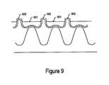
- FIG. 9shows the cross-sectional view of an embodiment of the memory device after sacrificial top oxide recess.
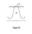
- FIG. 10shows the cross-sectional view of the memory device after performing the HDP recess and sacrificial top oxide removal.
- FIG. 11shows the cross-sectional view of the self-aligned memory device with rounded corners according to one embodiment of the present invention.
- FIG. 12is a flow diagram showing the process for two periphery integration schemes.
- FIG. 13shows a system according to embodiments of the present invention.
- the present inventionprovides a method for manufacturing a self-aligned memory device with generally rounded polysilicon and STI corners.
- Semiconductor non-volatile memory devicessuch as NOR-type and NAND-type flash memories, can be constructed using oxide/nitride/oxide (ONO) configurations.
- the nitride layere.g., silicon nitride, silicon rich nitride, or multiple layers with different percentages of Si content
- FIGS. 2 and 3show the process flows for fabricating the memory device according to one embodiment of the present invention.
- a barrier oxide layeris formed on a silicon substrate, step 201 .
- the barrier oxidecan be grown or deposited over the substrate.
- a nitride layeris then formed in step 202 .
- a core source/drain maskis patterned in step 203 .
- the core STI etchthen follows, step 204 .
- FIG. 4shows the STI profile after the STI etch is performed.
- the STI processdefines a number of active regions 401 separated by trenches 402 over a common substrate 403 .
- the oxide 404 and nitride 403 from steps 201 and 202reside on active regions 401 .
- Active regions 401are regions where the transistor action occurs.
- Substrate 403can be fabricated from silicon, silicon based composites, or other known semiconductor materials including, but not limited to polysilicon, germanium, silicon germanium, Semiconductor-On-Insulator (SOI) material, etc. It should be noted that the conductivity type of substrate 403 is not a limitation of the present invention. In accordance with one embodiment, the conductivity type is chosen to form an N-channel insulated gate field effect transistor. However, the conductivity type can be selected to form a P-channel insulated gate semiconductor device or a complementary insulated gate semiconductor device (e.g., CMOS).
- CMOScomplementary insulated gate semiconductor device
- a peripheral source/drain masking (SDM) step 205is performed.
- the peripheral STI etching step 206follows.
- the peripheral SDM and STI etchcan be combined with core SDM and STI etch, respectively.
- one or more liner oxide layersare formed with or without wet etch of existing oxide before each liner oxide to round up the STI corners, and in step 208 , an STI fill is performed. It is the combination of one or more liner oxide and/or cleaning processes which causes the corners of the STI to become rounded. It should be noted that other known processes for rounding the corners can be employed at this time.
- the STI trenchwas cut after substantially all the layers (including the charge-trapping layers) were formed.
- FIG. 5shows a cross-sectional side view of one embodiment of the memory device after STI fill step 208 .
- the filling 500can be an insulator material, such as an oxide formed by a high density plasma process.
- This trench fill material 500is polished back in step 209 .
- the nitrideis stripped in step 210 .
- One or more sacrificial oxide layers with or without wet etch of existing oxide before each sacrificial oxideare performed in step 211 .
- the sacrificial oxidecan also be skipped.
- the sacrificial oxide or the barrier oxide in case that sacrificial oxide is skipped,is then removed by a bottom oxide pre-clean step 217 .
- the oxide removalcan be done in a variety of ways. It can be accomplished, for example, by means of wet or dry etch, sputtering, plasma techniques, or by other means.
- FIG. 6shows a cross-sectional view of one embodiment of the memory device after the nitride strip, sacrificial oxide and bottom oxide pre-cleaning. It should be noted that the corners 601 and 602 are now rounded.
- a charge trapping structureis fabricated.
- thisentails growing a bottom oxide layer, as indicated by step 213 .
- a silicon-rich nitride (SiRN) or multiple layers of nitride with different percentages of Si contentare deposited on top of the bottom oxide layer in step 214 .
- a sacrificial top oxide processis then performed over the SiRN layer in step 215 .
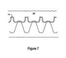
- FIG. 7shows a cross-sectional view of the memory device as it exists after the sacrificial top oxide deposition/process of step 215 .
- the silicon-rich nitride (SiRN)is depicted as layer 701 .
- the sacrificial top oxideis 702 .
- the sacrificial top oxidewill be completely etched off in step 219 .
- the top oxidewill be formed in step 1204 or 1215 described below in reference to FIG. 12 .
- any charge trapping structureincluding but not limited to ONO, can be utilized within the scope of the present invention.
- Other charge trapping structurescan include three or more dielectric layers disposed on the active regions.
- the top and bottom dielectric layersmay be silicon dioxide layers that are oxygen-rich silicon dioxide layers; one or both of which may be thermally grown or deposited oxide layers.
- one or both of the bottom and top dielectric layersmay be silicon dioxide layers that are nitrided oxide layers.
- the middle dielectric layermay be a silicon-rich silicon nitride layer or a combination of multiple layers with different percentages of Si content.
- the charge trapping structureis not limited to being a three layer structure or a structure limited to silicon dioxide and silicon nitride.
- the charge trapping structuremay be any dielectric layer or layers capable of trapping charge or that facilitate charge trapping.
- suitable materialsinclude an oxide/nitride bilayer dielectric, a nitride/oxide bilayer dielectric, an oxide/tantalum oxide bilayer dielectric (SiO 2 /Ta 2 O 5 ), an oxide/tantalum oxide/oxide trilayer dielectric (SiO 2 /Ta 2 O 5 /SiO 2 ), an oxide/strontium titanate bilayer dielectric (SiO 2 /SrTiO 3 ), an oxide/barium strontium titanate bilayer dielectric (SiO 2 /BaSrTiO 2 ), an oxide/strontium titanate/oxide trilayer dielectric, an oxide/strontium titanate/oxide trilayer dielectric (SiO 2 /SrTiO
- the sacrificial top oxideis polished back by CMP or etched back by plasma dry etch.
- CMPchemical mechanical planarization
- Other suitable planarization techniquesinclude electropolishing, electrochemical polishing, chemical polishing, and chemically enhanced planarization.
- FIG. 8shows a cross-sectional view of an embodiment of the memory device using a CMP technique whereby the sacrificial top oxide layers are polished back to the boundary 801 of the SiRN layer.
- the SiRN layeris approximately 60 to 130 angstroms thick as deposit and final thickness can be approximately 30 to 100 angstroms thick.
- a sacrificial top oxide recessis performed in step 217 .
- the recesscan be performed by either a wet or dry etching process.
- FIG. 9shows the cross-sectional view of an embodiment of the memory device after recess. As shown, the oxide 901 is now recessed below the tops 902 of the SiRN layer over the active regions. Next, the SiRN is wet or dry etched, step 218 . This is done to separate the SiRN layers for each memory cell. In other words, the top portions of the SiRN layers are etched off so that each active region has its own separate SiRN layer. A sacrificial top oxide removal is performed in step 219 . The cross-sectional view of the memory device after performing the sacrificial top oxide removal is shown in FIG.
- the SiRN portion 1001is segmented over the active region 1002 . Furthermore, the combination of the sacrificial top oxide, polish and wet etch of the nitride makes the new integration scheme self-aligned according to this embodiment of the present invention. It should be noted that TEOS is one of the films that can be used for the sacrificial top oxide.
- a thick ( 200 - 400 A) and a thin ( 20 - 100 A) gate oxideare needed for periphery transistors of NAND or NOR flash memory.
- Two approaches for periphery transistor gate oxideare shown in FIG. 12 and described later below.
- an ONO maskopens the periphery area. Dry or wet or a combination of dry and wet etch removes ONO layers in the periphery. A dry thick gate oxide is grown first. Gate oxide mask opens thin gate oxide area and a wet or dry etch removes the thick oxide and then a thin gate oxide is grown.
- the other approachis for wet periphery thick oxide. Since during the wet oxidation oxygen diffuses through oxide in core STI area and encroaches core S/D, a thin ( 20 - 30 A) SiRN or nitride is deposited first to block the steam oxide. An ONO mask opens the periphery area. Dry or wet or a combination of dry and wet etch removes ONO layers in the periphery. A thick steam gate oxide grows first and is followed by SPA top oxide. This SPA top oxide adds the thickness to the steam oxide and also consumes all the thin SiRN or nitride on core STI. Gate oxide mask opens thin gate oxide area and a wet or dry etch removes the thick oxide and then a thin gate oxide is grown.
- FIG. 11shows the cross-sectional view of the self-aligned memory device with rounded corners according to one embodiment of the present invention.
- Each active region 1101 - 1103is separated on each side by trenches 1104 - 1107 .
- the trenchesare formed through an STI process as described above. Right after the STI process, the corners of these active regions 1101 - 1103 are sharp due to the way the trenches are vertically cut.
- the cornersare rounded. It is advantageous to round the corners at this time because they are exposed.
- the rounding processcan be done in may different ways, such as by means of known cleaning/polishing and/or sacrificial oxide placement/removal.
- the corners 1108 - 1114are rounded before any additional layers are formed. After the corners have sufficiently been rounded, any number or combination of layers can be deposited or grown over the active region. For example, a tunnel oxide layer (optional), ONO (ONO stands for tunnel oxide-nitride-top oxide) stacks 1115 - 1117 , polysilicon layer(s) 1118 , etc. can be formed after the rounding process.
- a tunnel oxide layeroptional
- ONOstands for tunnel oxide-nitride-top oxide
- polysilicon layer(s) 1118etc.
- steps 213 - 219 shown in the flow diagram of FIG. 2is of particular relevance because these steps depict the process of forming self-aligned ONO stacks.
- the stepsstart with a bottom oxide. This is followed by depositing the SiRN. A sacrificial top oxide deposition is performed. The sacrificial top oxide is polished or etched back. A sacrificial oxide recess is performed, and a SiRN wet or dry etch is performed. This results in a self-aligned process which greatly improves scalability.
- FIG. 12is a flow diagram showing the process for two periphery integration schemes.
- a sacrificial oxide removal step 1201is performed.
- step 1202is the same step as step 219 of FIG. 3 .
- a first periphery integration scheme 1202includes process steps 1204 - 1210 .
- an SPA or high temperature oxidation (HTO)is used to form a top oxide.
- An ONO maskingis performed in step 1205 .
- the ONOis etched in step 1206 .
- a periphery thick gate oxideis fabricated in step 1207 .
- the gate oxideis masked in step 1208 .
- the gate oxideis then etched in step 1209 .
- a periphery thin gate oxideis fabricated in step 1210 .
- a second periphery integration scheme 1203includes process steps 1211 - 1218 .
- step 1211a thin SiRN or Nitride layer is deposited.
- An ONO masking step 1212is then performed.
- the ONOis then etched in step 1213 .
- a periphery thick gate oxide layeris fabricated in step 1214 .
- An SPA top oxideis fabricated in step 1215 .
- the gate oxideis then masked in step 1216 .
- the gate oxideis etched in step 1217 .
- a periphery thin gate oxideis fabricated in step 1218 .
- a polysilicon layeris deposited in step 1219 .
- FIG. 13shows a system according to embodiments of the present invention.
- the system 1300can be a portable multimedia device, media player, communications device, networking devices, computing device, consumer electronic device, mobile computing device, image capture device, audio/visual device, gaming console, etc.
- System 1300includes a process 1302 that pertains to a microprocessor or controller for controlling the overall processing of data in system 1300 .
- Digital datais stored in a file system 1304 and a cache memory 1306 .
- the file system 1304typically provides high capacity storage capability for system 1300 .
- File system 1304can include a non-volatile flash memory 1330 . Flash memory 1330 has rounded STI corners and is manufactured as described above.
- the system 1300also includes volatile random access memory (RAM) 1320 and non-volatile read-only memory (ROM) 1322 for storing digital data.
- System 1300also includes a user input device 1308 , such as a button, keypad, dial, scroll wheel, touch sensitive pad, etc.
- a display 1310is used to display visual information to the user.
- a data bus 1324transfers data between the various components via a bus interface 1318 .
- a compression-decompression (CODEC) chipcan be used to facilitate data storage and transfers.
- a speaker 1314is used to play back songs, voice messages, and other audio streams.
- a non-volatile, self-aligned semiconductor memory device having rounded STI corners and a method for manufacturing the devicehas been disclosed.
- the STI processis performed before the ONO and polysilicon deposition steps. This enables the STI corners to be rounded after the STI process but before the ONO and polysilicon deposition steps.
- Thisis in contrast to the conventional method of forming ONO and polysilicon before the STI definition.
- the convention methodafter the STI formation, another polysilicon is deposited on the previous polysilicon layer and then the word line is defined. This conventional method results in sharp polysilicon and STI corners which degrades device performance and reliability.
- the present inventionmitigates the disadvantageous attributes corresponding to the sharp corners resulting from conventional fabrication techniques. Moreover, the present invention has greater scalability due to the fact that it is self-aligned. This is accomplished by means of a sacrificial top oxide, polish, and wet etch of the nitride. Although not shown, it should be appreciated that source and drain regions are formed in active regions of the substrate and that additional processing is performed to form a metallization system including contact structures.
Landscapes
- Engineering & Computer Science (AREA)
- Physics & Mathematics (AREA)
- Condensed Matter Physics & Semiconductors (AREA)
- General Physics & Mathematics (AREA)
- Manufacturing & Machinery (AREA)
- Computer Hardware Design (AREA)
- Microelectronics & Electronic Packaging (AREA)
- Power Engineering (AREA)
- Non-Volatile Memory (AREA)
- Semiconductor Memories (AREA)
Abstract
Description
Claims (12)
Priority Applications (3)
| Application Number | Priority Date | Filing Date | Title |
|---|---|---|---|
| US11/639,667US8642441B1 (en) | 2006-12-15 | 2006-12-15 | Self-aligned STI with single poly for manufacturing a flash memory device |
| US14/167,845US9276007B2 (en) | 2006-12-15 | 2014-01-29 | System and method for manufacturing self-aligned STI with single poly |
| US14/865,563US10622370B1 (en) | 2006-12-15 | 2015-09-25 | System and method for manufacturing self-aligned STI with single poly |
Applications Claiming Priority (1)
| Application Number | Priority Date | Filing Date | Title |
|---|---|---|---|
| US11/639,667US8642441B1 (en) | 2006-12-15 | 2006-12-15 | Self-aligned STI with single poly for manufacturing a flash memory device |
Related Child Applications (2)
| Application Number | Title | Priority Date | Filing Date |
|---|---|---|---|
| US12/699,635Continuation-In-PartUS8551858B2 (en) | 2010-02-03 | 2010-02-03 | Self-aligned SI rich nitride charge trap layer isolation for charge trap flash memory |
| US14/167,845DivisionUS9276007B2 (en) | 2006-12-15 | 2014-01-29 | System and method for manufacturing self-aligned STI with single poly |
Publications (1)
| Publication Number | Publication Date |
|---|---|
| US8642441B1true US8642441B1 (en) | 2014-02-04 |
Family
ID=50002947
Family Applications (3)
| Application Number | Title | Priority Date | Filing Date |
|---|---|---|---|
| US11/639,667Active2027-12-01US8642441B1 (en) | 2006-12-15 | 2006-12-15 | Self-aligned STI with single poly for manufacturing a flash memory device |
| US14/167,845ActiveUS9276007B2 (en) | 2006-12-15 | 2014-01-29 | System and method for manufacturing self-aligned STI with single poly |
| US14/865,563ActiveUS10622370B1 (en) | 2006-12-15 | 2015-09-25 | System and method for manufacturing self-aligned STI with single poly |
Family Applications After (2)
| Application Number | Title | Priority Date | Filing Date |
|---|---|---|---|
| US14/167,845ActiveUS9276007B2 (en) | 2006-12-15 | 2014-01-29 | System and method for manufacturing self-aligned STI with single poly |
| US14/865,563ActiveUS10622370B1 (en) | 2006-12-15 | 2015-09-25 | System and method for manufacturing self-aligned STI with single poly |
Country Status (1)
| Country | Link |
|---|---|
| US (3) | US8642441B1 (en) |
Families Citing this family (2)
| Publication number | Priority date | Publication date | Assignee | Title |
|---|---|---|---|---|
| KR102442309B1 (en) | 2015-07-09 | 2022-09-13 | 삼성전자주식회사 | Methods of forming an isolation structure in a semiconductor device |
| KR102406977B1 (en) | 2015-07-16 | 2022-06-10 | 삼성전자주식회사 | Methods of manufacturing semiconductor devices including isolation layers |
Citations (85)
| Publication number | Priority date | Publication date | Assignee | Title |
|---|---|---|---|---|
| US4935378A (en)* | 1987-03-23 | 1990-06-19 | Kabushiki Kaisha Toshiba | Method for manufacturing a semiconductor device having more than two conductive layers |
| US4980309A (en)* | 1987-11-30 | 1990-12-25 | Texas Instruments, Incorporated | Method of making high density EEPROM |
| US5173436A (en)* | 1989-11-21 | 1992-12-22 | Texas Instruments Incorporated | Method of manufacturing an EEPROM with trench-isolated bitlines |
| US5523249A (en)* | 1990-08-01 | 1996-06-04 | Texas Instruments Incorporated | Method of making an EEPROM cell with separate erasing and programming regions |
| US5966603A (en)* | 1997-06-11 | 1999-10-12 | Saifun Semiconductors Ltd. | NROM fabrication method with a periphery portion |
| US6001704A (en)* | 1998-06-04 | 1999-12-14 | Vanguard International Semiconductor Corporation | Method of fabricating a shallow trench isolation by using oxide/oxynitride layers |
| US6127215A (en)* | 1998-10-29 | 2000-10-03 | International Business Machines Corp. | Deep pivot mask for enhanced buried-channel PFET performance and reliability |
| US6146975A (en)* | 1998-07-10 | 2000-11-14 | Lucent Technologies Inc. | Shallow trench isolation |
| US6153494A (en)* | 1999-05-12 | 2000-11-28 | Taiwan Semiconductor Manufacturing Company | Method to increase the coupling ratio of word line to floating gate by lateral coupling in stacked-gate flash |
| US6159801A (en)* | 1999-04-26 | 2000-12-12 | Taiwan Semiconductor Manufacturing Company | Method to increase coupling ratio of source to floating gate in split-gate flash |
| US6166409A (en)* | 1996-09-13 | 2000-12-26 | Alliance Semiconductor Corporation | Flash EPROM memory cell having increased capacitive coupling |
| US6184085B1 (en)* | 1998-07-03 | 2001-02-06 | Samsung Electronics Co., Ltd. | Methods of forming nonvolatile memory devices using improved masking techniques |
| US6204530B1 (en)* | 1998-08-13 | 2001-03-20 | Samsung Electronics, Co., Ltd. | Flash-type nonvolatile semiconductor memory devices for preventing overerasure |
| US6207490B1 (en)* | 1997-12-11 | 2001-03-27 | Samsung Electronics Co., Ltd. | Semiconductor device and method for fabricating the same |
| US6222225B1 (en)* | 1998-09-29 | 2001-04-24 | Kabushiki Kaisha Toshiba | Semiconductor device and manufacturing method thereof |
| US6258669B1 (en)* | 1997-12-18 | 2001-07-10 | Advanced Micro Devices, Inc. | Methods and arrangements for improved formation of control and floating gates in non-volatile memory semiconductor devices |
| US6281050B1 (en)* | 1999-03-15 | 2001-08-28 | Kabushiki Kaisha Toshiba | Manufacturing method of a semiconductor device and a nonvolatile semiconductor storage device |
| US6355514B1 (en)* | 2000-02-10 | 2002-03-12 | Advanced Micro Devices, Inc. | Dual bit isolation scheme for flash devices |
| US6395592B1 (en)* | 2000-10-24 | 2002-05-28 | Silicon-Based Technology Corp. | Methods for fabricating scalable non-volatile semiconductor memory device with double-sides erase cathodes |
| US6403421B1 (en)* | 1998-04-22 | 2002-06-11 | Sony Corporation | Semiconductor nonvolatile memory device and method of producing the same |
| US6417047B1 (en)* | 1999-09-20 | 2002-07-09 | Kabushiki Kaisha Toshiba | Manufacturing method of a non-volatile semiconductor memory device having isolation regions |
| US6448606B1 (en)* | 2000-02-24 | 2002-09-10 | Advanced Micro Devices, Inc. | Semiconductor with increased gate coupling coefficient |
| US20020132427A1 (en)* | 2001-01-24 | 2002-09-19 | Rudeck Paul J. | Modified source/drain re-oxidation method and system |
| US20020153557A1 (en)* | 2000-08-16 | 2002-10-24 | Fairchild Semiconductor Corporation | Method for creating thick oxide on the bottom surface of a trench structure in silicon |
| US6486508B1 (en)* | 1999-05-12 | 2002-11-26 | Samsung Electronics Co., Ltd. | Non-volatile semiconductor memory devices with control gates overlapping pairs of floating gates |
| US20020179962A1 (en)* | 2001-06-01 | 2002-12-05 | Kabushiki Kaisha Toshiba | Semiconductor device having floating gate and method of producing the same |
| US20030013255A1 (en)* | 2000-11-30 | 2003-01-16 | Bohumil Lojek | Method of fabricating a self-aligned non-volatile memory cell |
| US6555427B1 (en)* | 1999-08-31 | 2003-04-29 | Kabushiki Kaisha Toshiba | Non-volatile semiconductor memory device and manufacturing method thereof |
| US20030080372A1 (en)* | 2001-10-30 | 2003-05-01 | Thomas Mikolajick | Semiconductor memory cell, method for fabricating the memory cell, and semiconductor memory device |
| US20030111687A1 (en)* | 2001-12-18 | 2003-06-19 | Josef Willer | Memory cell with trench transistor |
| US20030119314A1 (en)* | 2001-12-20 | 2003-06-26 | Jusuke Ogura | Monos device having buried metal silicide bit line |
| US20030181020A1 (en)* | 1997-02-18 | 2003-09-25 | Norio Ishitsuka | Semiconductor device and process for producing the same |
| US20030208663A1 (en)* | 2002-04-12 | 2003-11-06 | Van Buskirk Michael A. | System and method for multi-bit flash reads using dual dynamic references |
| US20030209760A1 (en)* | 2002-05-10 | 2003-11-13 | Nec Electronics Corporation | Semiconductor integrated circuit and method of fabricating the same |
| US6649472B1 (en)* | 2002-08-02 | 2003-11-18 | Taiwan Semiconductor Manufacturing Company | Method of manufacturing a flash memory cell with high programming efficiency by coupling from floating gate to sidewall |
| US6677224B2 (en)* | 2001-10-12 | 2004-01-13 | Horng-Huei Tseng | Method of forming stacked gate for flash memories |
| US6682978B1 (en)* | 1999-08-30 | 2004-01-27 | Advanced Micro Devices, Inc. | Integrated circuit having increased gate coupling capacitance |
| US20040048433A1 (en)* | 2002-08-30 | 2004-03-11 | Fujitsu Limited | Method of manufacturing a memory integrated circuit device |
| US6709924B1 (en)* | 2002-11-12 | 2004-03-23 | Advanced Micro Devices, Inc. | Fabrication of shallow trench isolation structures with rounded corner and self-aligned gate |
| US6720610B2 (en)* | 1999-12-09 | 2004-04-13 | Kabushiki Kaisha Toshiba | Nonvolatile semiconductor memory device and its manufacturing method |
| US20040082141A1 (en)* | 2002-10-29 | 2004-04-29 | Toshikazu Mizukoshi | Method of fabricating a semiconductor device having trenches |
| US20040097080A1 (en)* | 2002-11-18 | 2004-05-20 | Kim Jum Soo | Method of manufacturing a semiconductor device |
| US6743675B2 (en)* | 2002-10-01 | 2004-06-01 | Mosel Vitelic, Inc. | Floating gate memory fabrication methods comprising a field dielectric etch with a horizontal etch component |
| US20040145007A1 (en)* | 2003-01-24 | 2004-07-29 | Renesas Technology Corp. | Non-volatile semiconductor memory device and method of fabricating the same |
| US6781189B2 (en)* | 2002-01-22 | 2004-08-24 | Micron Technology, Inc. | Floating gate transistor with STI |
| US6825128B2 (en)* | 2002-06-14 | 2004-11-30 | Nec Electronics Corporation | Method for manufacturing semiconductor device |
| US20040253831A1 (en)* | 2003-06-10 | 2004-12-16 | Mosel Vitelic, Inc. | Method of forming rounded corner in trench |
| US6891246B2 (en)* | 2001-06-26 | 2005-05-10 | Kabushiki Kaisha Toshiba | Nonvolatile semiconductor memory and manufacturing method thereof |
| US6894339B2 (en)* | 2003-01-02 | 2005-05-17 | Actrans System Inc. | Flash memory with trench select gate and fabrication process |
| US6900100B2 (en)* | 1999-05-25 | 2005-05-31 | Advanced Analogic Technologies, Inc. | Trench semiconductor device having gate oxide layer with multiple thicknesses and processes of fabricating the same |
| US20050142765A1 (en)* | 2003-12-30 | 2005-06-30 | Hynix Semiconductor Inc. | Method for manufacturing flash memory device |
| US20050186739A1 (en)* | 2002-05-24 | 2005-08-25 | Hynix Semiconductor Inc. | Flash memory device having poly spacers |
| US20050189582A1 (en)* | 2004-02-10 | 2005-09-01 | Thomas Mikolajick | Charge trapping memory cell and fabrication method |
| US20050287763A1 (en)* | 2004-06-29 | 2005-12-29 | Taek-Jung Kim | Method of manufacturing a semiconductor device |
| US7005714B2 (en)* | 2003-07-04 | 2006-02-28 | Kabushiki Kaisha Toshiba | Nonvolatile semiconductor memory and manufacturing method for the same |
| US7009245B2 (en)* | 2002-12-24 | 2006-03-07 | Macronix International Co., Ltd. | High-K tunneling dielectric for read only memory device and fabrication method thereof |
| US7015099B2 (en)* | 2001-12-22 | 2006-03-21 | Hynix Semiconductor, Inc. | Method of manufacturing a flash memory cell capable of increasing a coupling ratio |
| US20060099755A1 (en)* | 2000-06-09 | 2006-05-11 | Kabushiki Kaisha Toshiba | Semiconductor memory integrated circuit and its manufacturing method |
| US7067377B1 (en)* | 2004-03-30 | 2006-06-27 | Fasl Llc | Recessed channel with separated ONO memory device |
| US20060163202A1 (en)* | 2005-01-21 | 2006-07-27 | Tokyo Electron Limited | Plasma etching method |
| US7087950B2 (en)* | 2004-04-30 | 2006-08-08 | Infineon Technologies Ag | Flash memory cell, flash memory device and manufacturing method thereof |
| US7091091B2 (en)* | 2004-06-28 | 2006-08-15 | Promos Technologies Inc. | Nonvolatile memory fabrication methods in which a dielectric layer underlying a floating gate layer is spaced from an edge of an isolation trench and/or an edge of the floating gate layer |
| US7135737B2 (en)* | 2003-12-31 | 2006-11-14 | Dongbu Electronics Co., Ltd. | Non-volatile flash memory device |
| US20060270156A1 (en)* | 2004-10-08 | 2006-11-30 | Seong-Gyun Kim | Non-volatile memory devices and methods of forming the same |
| US7151295B2 (en)* | 2004-05-18 | 2006-12-19 | Kabushiki Kaisha Toshiba | Non-volatile semiconductor memory device and process of manufacturing the same |
| US20060289924A1 (en)* | 2005-06-28 | 2006-12-28 | Chih-Hsin Wang | Low power electrically alterable nonvolatile memory cells and arrays |
| US20060291281A1 (en)* | 2005-06-27 | 2006-12-28 | Pin-Yao Wang | Non-volatile memory, manufacturing and operating method thereof |
| US20070023815A1 (en)* | 2005-07-27 | 2007-02-01 | Dong-Yean Oh | Non-volatile memory device and associated method of manufacture |
| US20070023792A1 (en)* | 2005-07-01 | 2007-02-01 | Sharp Kabushiki Kaisha | Transistor and transistor manufacturing method |
| US20070026632A1 (en)* | 2005-07-26 | 2007-02-01 | Elpida Memory Inc. | Method of manufacturing a semiconductor device and the semiconductor device |
| US7189627B2 (en)* | 2004-08-19 | 2007-03-13 | Texas Instruments Incorporated | Method to improve SRAM performance and stability |
| US7205602B2 (en)* | 2002-08-20 | 2007-04-17 | Taiwan Semiconductor Manufacturing Co., Ltd. | Method to improve the coupling ratio of top gate to floating gate in flash |
| US20070087523A1 (en)* | 2005-10-13 | 2007-04-19 | Macronix International Co., Ltd. | Recessed shallow trench isolation |
| US20070099369A1 (en)* | 2005-10-31 | 2007-05-03 | Semiconductor Manufacturing International (Shanghai) Corporation | Integration scheme method and structure for transistors using strained silicon |
| US7297595B2 (en)* | 2003-12-27 | 2007-11-20 | Dongbu Hitek Co., Ltd. | Non-volatile memory device and fabricating method thereof |
| US20080084765A1 (en)* | 2006-10-03 | 2008-04-10 | Kuo-Tung Chang | Method and apparatus for sector erase operation in a flash memory array |
| US7358145B2 (en)* | 2006-06-15 | 2008-04-15 | Macronix International Co., Ltd. | Method of fabricating shallow trench isolation structure |
| US20080128774A1 (en)* | 2006-11-02 | 2008-06-05 | Rustom Irani | Forming silicon trench isolation (STI) in semiconductor devices self-aligned to diffusion |
| US7399674B2 (en)* | 2004-10-22 | 2008-07-15 | Macronix International Co., Ltd. | Method of fabricating NAND-type flash EEPROM without field oxide isolation |
| US20080171416A1 (en)* | 2007-01-12 | 2008-07-17 | Shenging Fang | Self-aligned patterning method by using non-conformal film and etch back for flash memory and other semiconductor applications |
| US7494869B2 (en)* | 2005-05-13 | 2009-02-24 | Kabushiki Kaisha Toshiba | Semiconductor integrated circuit device and manufacturing method thereof |
| US20100244247A1 (en)* | 2009-03-27 | 2010-09-30 | Taiwan Semiconductor Manufacturing Company, Ltd. | Via structure and via etching process of forming the same |
| US7985651B2 (en)* | 2008-01-03 | 2011-07-26 | Samsung Electronics Co., Ltd. | Method of fabricating semiconductor device having differential gate dielectric layer and related device |
| US8008153B2 (en)* | 2002-07-05 | 2011-08-30 | Samsung Electronics Co., Ltd. | Methods of fabricating nonvolatile memory devices having gate structures doped by nitrogen |
| US8173515B2 (en)* | 2008-07-22 | 2012-05-08 | Elpida Memory, Inc. | Method for manufacturing semiconductor device |
Family Cites Families (32)
| Publication number | Priority date | Publication date | Assignee | Title |
|---|---|---|---|---|
| JPH0821638B2 (en)* | 1989-12-15 | 1996-03-04 | 株式会社東芝 | Nonvolatile semiconductor memory device and manufacturing method thereof |
| US5393694A (en)* | 1994-06-15 | 1995-02-28 | Micron Semiconductor, Inc. | Advanced process for recessed poly buffered locos |
| KR0144902B1 (en)* | 1995-04-17 | 1998-07-01 | 김광호 | Nonvolatile Memory Device and Manufacturing Method |
| KR100199382B1 (en)* | 1996-06-27 | 1999-06-15 | 김영환 | Manufacturing Method of Flash Memory Device |
| JP3710880B2 (en)* | 1996-06-28 | 2005-10-26 | 株式会社東芝 | Nonvolatile semiconductor memory device |
| US6297096B1 (en)* | 1997-06-11 | 2001-10-02 | Saifun Semiconductors Ltd. | NROM fabrication method |
| US6162683A (en)* | 1997-12-19 | 2000-12-19 | Texas Instruments Incorporated | System and method for forming an inter-layer dielectric in floating gate memory devices |
| US6825544B1 (en)* | 1998-12-09 | 2004-11-30 | Cypress Semiconductor Corporation | Method for shallow trench isolation and shallow trench isolation structure |
| US6140182A (en)* | 1999-02-23 | 2000-10-31 | Actrans System Inc. | Nonvolatile memory with self-aligned floating gate and fabrication process |
| US6406960B1 (en)* | 1999-10-25 | 2002-06-18 | Advanced Micro Devices, Inc. | Process for fabricating an ONO structure having a silicon-rich silicon nitride layer |
| US6727161B2 (en)* | 2000-02-16 | 2004-04-27 | Cypress Semiconductor Corp. | Isolation technology for submicron semiconductor devices |
| US6500768B1 (en)* | 2000-10-30 | 2002-12-31 | Advance Micro Devices, Inc. | Method for selective removal of ONO layer |
| US6468865B1 (en)* | 2000-11-28 | 2002-10-22 | Advanced Micro Devices, Inc. | Method of simultaneous formation of bitline isolation and periphery oxide |
| US6534363B2 (en)* | 2001-03-12 | 2003-03-18 | Advanced Micro Devices, Inc. | High voltage oxidation method for highly reliable flash memory devices |
| US6806163B2 (en)* | 2002-07-05 | 2004-10-19 | Taiwan Semiconductor Manufacturing Co., Ltd | Ion implant method for topographic feature corner rounding |
| KR100452037B1 (en)* | 2002-07-18 | 2004-10-08 | 주식회사 하이닉스반도체 | Method for manufacturing semiconductor device and the device |
| JP2004095889A (en)* | 2002-08-30 | 2004-03-25 | Fasl Japan Ltd | Semiconductor storage device and method of manufacturing the same |
| JP2004095918A (en)* | 2002-08-30 | 2004-03-25 | Fasl Japan Ltd | Semiconductor storage device and method of manufacturing semiconductor device |
| US7648881B2 (en)* | 2003-01-10 | 2010-01-19 | Samsung Electronics Co., Ltd. | Non-volatile memory devices with charge storage insulators and methods of fabricating such devices |
| KR100504691B1 (en)* | 2003-01-10 | 2005-08-03 | 삼성전자주식회사 | Non-volatile memory device having a charge strage insulator and method of fabricating the same |
| DE10333549B3 (en)* | 2003-07-23 | 2005-01-13 | Infineon Technologies Ag | Charge trapping memory cell used as transistor comprises semiconductor body or substrate having upper side with curve in channel region |
| US6958272B2 (en)* | 2004-01-12 | 2005-10-25 | Advanced Micro Devices, Inc. | Pocket implant for complementary bit disturb improvement and charging improvement of SONOS memory cell |
| US20060046402A1 (en)* | 2004-08-31 | 2006-03-02 | Micron Technology, Inc. | Flash cell structures and methods of formation |
| US20060094257A1 (en)* | 2004-11-04 | 2006-05-04 | Tower Semiconductor Ltd. | Low thermal budget dielectric stack for SONOS nonvolatile memories |
| US20070045717A1 (en)* | 2005-08-31 | 2007-03-01 | Stefano Parascandola | Charge-trapping memory device and method of production |
| KR100672829B1 (en)* | 2005-08-31 | 2007-01-22 | 삼성전자주식회사 | Manufacturing method of charge trap insulator and manufacturing method of non-volatile memory device of sonos type |
| US20070077748A1 (en)* | 2005-09-30 | 2007-04-05 | Dominik Olligs | Method for forming a semiconductor product and semiconductor product |
| US8803216B2 (en)* | 2006-03-20 | 2014-08-12 | Spansion, Llc | Memory cell system using silicon-rich nitride |
| US20070247924A1 (en)* | 2006-04-06 | 2007-10-25 | Wei Zheng | Methods for erasing memory devices and multi-level programming memory device |
| US7452766B2 (en)* | 2006-08-31 | 2008-11-18 | Micron Technology, Inc. | Finned memory cells and the fabrication thereof |
| US20080079061A1 (en)* | 2006-09-28 | 2008-04-03 | Advanced Micro Devices, Inc. | Flash memory cell structure for increased program speed and erase speed |
| US8173535B2 (en) | 2009-12-21 | 2012-05-08 | Omnivision Technologies, Inc. | Wafer structure to reduce dark current |
- 2006
- 2006-12-15USUS11/639,667patent/US8642441B1/enactiveActive
- 2014
- 2014-01-29USUS14/167,845patent/US9276007B2/enactiveActive
- 2015
- 2015-09-25USUS14/865,563patent/US10622370B1/enactiveActive
Patent Citations (92)
| Publication number | Priority date | Publication date | Assignee | Title |
|---|---|---|---|---|
| US4935378A (en)* | 1987-03-23 | 1990-06-19 | Kabushiki Kaisha Toshiba | Method for manufacturing a semiconductor device having more than two conductive layers |
| US4980309A (en)* | 1987-11-30 | 1990-12-25 | Texas Instruments, Incorporated | Method of making high density EEPROM |
| US5173436A (en)* | 1989-11-21 | 1992-12-22 | Texas Instruments Incorporated | Method of manufacturing an EEPROM with trench-isolated bitlines |
| US5523249A (en)* | 1990-08-01 | 1996-06-04 | Texas Instruments Incorporated | Method of making an EEPROM cell with separate erasing and programming regions |
| US6166409A (en)* | 1996-09-13 | 2000-12-26 | Alliance Semiconductor Corporation | Flash EPROM memory cell having increased capacitive coupling |
| US20030181020A1 (en)* | 1997-02-18 | 2003-09-25 | Norio Ishitsuka | Semiconductor device and process for producing the same |
| US20050196935A1 (en)* | 1997-02-18 | 2005-09-08 | Norio Ishitsuka | Semiconductor device and process for producing the same |
| US5966603A (en)* | 1997-06-11 | 1999-10-12 | Saifun Semiconductors Ltd. | NROM fabrication method with a periphery portion |
| US6207490B1 (en)* | 1997-12-11 | 2001-03-27 | Samsung Electronics Co., Ltd. | Semiconductor device and method for fabricating the same |
| US6258669B1 (en)* | 1997-12-18 | 2001-07-10 | Advanced Micro Devices, Inc. | Methods and arrangements for improved formation of control and floating gates in non-volatile memory semiconductor devices |
| US6403421B1 (en)* | 1998-04-22 | 2002-06-11 | Sony Corporation | Semiconductor nonvolatile memory device and method of producing the same |
| US6001704A (en)* | 1998-06-04 | 1999-12-14 | Vanguard International Semiconductor Corporation | Method of fabricating a shallow trench isolation by using oxide/oxynitride layers |
| US6184085B1 (en)* | 1998-07-03 | 2001-02-06 | Samsung Electronics Co., Ltd. | Methods of forming nonvolatile memory devices using improved masking techniques |
| US6146975A (en)* | 1998-07-10 | 2000-11-14 | Lucent Technologies Inc. | Shallow trench isolation |
| US6204530B1 (en)* | 1998-08-13 | 2001-03-20 | Samsung Electronics, Co., Ltd. | Flash-type nonvolatile semiconductor memory devices for preventing overerasure |
| US6222225B1 (en)* | 1998-09-29 | 2001-04-24 | Kabushiki Kaisha Toshiba | Semiconductor device and manufacturing method thereof |
| US6127215A (en)* | 1998-10-29 | 2000-10-03 | International Business Machines Corp. | Deep pivot mask for enhanced buried-channel PFET performance and reliability |
| US6281050B1 (en)* | 1999-03-15 | 2001-08-28 | Kabushiki Kaisha Toshiba | Manufacturing method of a semiconductor device and a nonvolatile semiconductor storage device |
| US6159801A (en)* | 1999-04-26 | 2000-12-12 | Taiwan Semiconductor Manufacturing Company | Method to increase coupling ratio of source to floating gate in split-gate flash |
| US6153494A (en)* | 1999-05-12 | 2000-11-28 | Taiwan Semiconductor Manufacturing Company | Method to increase the coupling ratio of word line to floating gate by lateral coupling in stacked-gate flash |
| US6486508B1 (en)* | 1999-05-12 | 2002-11-26 | Samsung Electronics Co., Ltd. | Non-volatile semiconductor memory devices with control gates overlapping pairs of floating gates |
| US6900100B2 (en)* | 1999-05-25 | 2005-05-31 | Advanced Analogic Technologies, Inc. | Trench semiconductor device having gate oxide layer with multiple thicknesses and processes of fabricating the same |
| US6682978B1 (en)* | 1999-08-30 | 2004-01-27 | Advanced Micro Devices, Inc. | Integrated circuit having increased gate coupling capacitance |
| US6555427B1 (en)* | 1999-08-31 | 2003-04-29 | Kabushiki Kaisha Toshiba | Non-volatile semiconductor memory device and manufacturing method thereof |
| US6417047B1 (en)* | 1999-09-20 | 2002-07-09 | Kabushiki Kaisha Toshiba | Manufacturing method of a non-volatile semiconductor memory device having isolation regions |
| US6720610B2 (en)* | 1999-12-09 | 2004-04-13 | Kabushiki Kaisha Toshiba | Nonvolatile semiconductor memory device and its manufacturing method |
| US6355514B1 (en)* | 2000-02-10 | 2002-03-12 | Advanced Micro Devices, Inc. | Dual bit isolation scheme for flash devices |
| US6448606B1 (en)* | 2000-02-24 | 2002-09-10 | Advanced Micro Devices, Inc. | Semiconductor with increased gate coupling coefficient |
| US20060099755A1 (en)* | 2000-06-09 | 2006-05-11 | Kabushiki Kaisha Toshiba | Semiconductor memory integrated circuit and its manufacturing method |
| US20020153557A1 (en)* | 2000-08-16 | 2002-10-24 | Fairchild Semiconductor Corporation | Method for creating thick oxide on the bottom surface of a trench structure in silicon |
| US6395592B1 (en)* | 2000-10-24 | 2002-05-28 | Silicon-Based Technology Corp. | Methods for fabricating scalable non-volatile semiconductor memory device with double-sides erase cathodes |
| US20030013255A1 (en)* | 2000-11-30 | 2003-01-16 | Bohumil Lojek | Method of fabricating a self-aligned non-volatile memory cell |
| US20020132427A1 (en)* | 2001-01-24 | 2002-09-19 | Rudeck Paul J. | Modified source/drain re-oxidation method and system |
| US20020179962A1 (en)* | 2001-06-01 | 2002-12-05 | Kabushiki Kaisha Toshiba | Semiconductor device having floating gate and method of producing the same |
| US6768161B2 (en)* | 2001-06-01 | 2004-07-27 | Kabushiki Kaisha Toshiba | Semiconductor device having floating gate and method of producing the same |
| US6891246B2 (en)* | 2001-06-26 | 2005-05-10 | Kabushiki Kaisha Toshiba | Nonvolatile semiconductor memory and manufacturing method thereof |
| US6677224B2 (en)* | 2001-10-12 | 2004-01-13 | Horng-Huei Tseng | Method of forming stacked gate for flash memories |
| US20030080372A1 (en)* | 2001-10-30 | 2003-05-01 | Thomas Mikolajick | Semiconductor memory cell, method for fabricating the memory cell, and semiconductor memory device |
| US20030111687A1 (en)* | 2001-12-18 | 2003-06-19 | Josef Willer | Memory cell with trench transistor |
| US20030119314A1 (en)* | 2001-12-20 | 2003-06-26 | Jusuke Ogura | Monos device having buried metal silicide bit line |
| US7015099B2 (en)* | 2001-12-22 | 2006-03-21 | Hynix Semiconductor, Inc. | Method of manufacturing a flash memory cell capable of increasing a coupling ratio |
| US6781189B2 (en)* | 2002-01-22 | 2004-08-24 | Micron Technology, Inc. | Floating gate transistor with STI |
| US20030208663A1 (en)* | 2002-04-12 | 2003-11-06 | Van Buskirk Michael A. | System and method for multi-bit flash reads using dual dynamic references |
| US20030209760A1 (en)* | 2002-05-10 | 2003-11-13 | Nec Electronics Corporation | Semiconductor integrated circuit and method of fabricating the same |
| US20050186739A1 (en)* | 2002-05-24 | 2005-08-25 | Hynix Semiconductor Inc. | Flash memory device having poly spacers |
| US6825128B2 (en)* | 2002-06-14 | 2004-11-30 | Nec Electronics Corporation | Method for manufacturing semiconductor device |
| US8008153B2 (en)* | 2002-07-05 | 2011-08-30 | Samsung Electronics Co., Ltd. | Methods of fabricating nonvolatile memory devices having gate structures doped by nitrogen |
| US6649472B1 (en)* | 2002-08-02 | 2003-11-18 | Taiwan Semiconductor Manufacturing Company | Method of manufacturing a flash memory cell with high programming efficiency by coupling from floating gate to sidewall |
| US6903408B2 (en)* | 2002-08-02 | 2005-06-07 | Taiwan Semiconductor Manufacturing Company | Flash memory cell with high programming efficiency by coupling from floating gate to sidewall |
| US7205602B2 (en)* | 2002-08-20 | 2007-04-17 | Taiwan Semiconductor Manufacturing Co., Ltd. | Method to improve the coupling ratio of top gate to floating gate in flash |
| US20040048433A1 (en)* | 2002-08-30 | 2004-03-11 | Fujitsu Limited | Method of manufacturing a memory integrated circuit device |
| US6743675B2 (en)* | 2002-10-01 | 2004-06-01 | Mosel Vitelic, Inc. | Floating gate memory fabrication methods comprising a field dielectric etch with a horizontal etch component |
| US20040082141A1 (en)* | 2002-10-29 | 2004-04-29 | Toshikazu Mizukoshi | Method of fabricating a semiconductor device having trenches |
| US6709924B1 (en)* | 2002-11-12 | 2004-03-23 | Advanced Micro Devices, Inc. | Fabrication of shallow trench isolation structures with rounded corner and self-aligned gate |
| US20040097080A1 (en)* | 2002-11-18 | 2004-05-20 | Kim Jum Soo | Method of manufacturing a semiconductor device |
| US7009245B2 (en)* | 2002-12-24 | 2006-03-07 | Macronix International Co., Ltd. | High-K tunneling dielectric for read only memory device and fabrication method thereof |
| US6894339B2 (en)* | 2003-01-02 | 2005-05-17 | Actrans System Inc. | Flash memory with trench select gate and fabrication process |
| US6906378B2 (en)* | 2003-01-24 | 2005-06-14 | Renesas Technology Corp. | Non-volatile semiconductor memory device and method of fabricating the same |
| US20040145007A1 (en)* | 2003-01-24 | 2004-07-29 | Renesas Technology Corp. | Non-volatile semiconductor memory device and method of fabricating the same |
| US20040253831A1 (en)* | 2003-06-10 | 2004-12-16 | Mosel Vitelic, Inc. | Method of forming rounded corner in trench |
| US7005714B2 (en)* | 2003-07-04 | 2006-02-28 | Kabushiki Kaisha Toshiba | Nonvolatile semiconductor memory and manufacturing method for the same |
| US7297595B2 (en)* | 2003-12-27 | 2007-11-20 | Dongbu Hitek Co., Ltd. | Non-volatile memory device and fabricating method thereof |
| US20050142765A1 (en)* | 2003-12-30 | 2005-06-30 | Hynix Semiconductor Inc. | Method for manufacturing flash memory device |
| US7135737B2 (en)* | 2003-12-31 | 2006-11-14 | Dongbu Electronics Co., Ltd. | Non-volatile flash memory device |
| US20050189582A1 (en)* | 2004-02-10 | 2005-09-01 | Thomas Mikolajick | Charge trapping memory cell and fabrication method |
| US7067377B1 (en)* | 2004-03-30 | 2006-06-27 | Fasl Llc | Recessed channel with separated ONO memory device |
| US7087950B2 (en)* | 2004-04-30 | 2006-08-08 | Infineon Technologies Ag | Flash memory cell, flash memory device and manufacturing method thereof |
| US7151295B2 (en)* | 2004-05-18 | 2006-12-19 | Kabushiki Kaisha Toshiba | Non-volatile semiconductor memory device and process of manufacturing the same |
| US7091091B2 (en)* | 2004-06-28 | 2006-08-15 | Promos Technologies Inc. | Nonvolatile memory fabrication methods in which a dielectric layer underlying a floating gate layer is spaced from an edge of an isolation trench and/or an edge of the floating gate layer |
| US20050287763A1 (en)* | 2004-06-29 | 2005-12-29 | Taek-Jung Kim | Method of manufacturing a semiconductor device |
| US7189627B2 (en)* | 2004-08-19 | 2007-03-13 | Texas Instruments Incorporated | Method to improve SRAM performance and stability |
| US20060270156A1 (en)* | 2004-10-08 | 2006-11-30 | Seong-Gyun Kim | Non-volatile memory devices and methods of forming the same |
| US20080224200A1 (en)* | 2004-10-22 | 2008-09-18 | Ming-Shang Chen | Method of fabricating nand-type flash eeprom without field oxide isolation |
| US7399674B2 (en)* | 2004-10-22 | 2008-07-15 | Macronix International Co., Ltd. | Method of fabricating NAND-type flash EEPROM without field oxide isolation |
| US20060163202A1 (en)* | 2005-01-21 | 2006-07-27 | Tokyo Electron Limited | Plasma etching method |
| US7494869B2 (en)* | 2005-05-13 | 2009-02-24 | Kabushiki Kaisha Toshiba | Semiconductor integrated circuit device and manufacturing method thereof |
| US20060291281A1 (en)* | 2005-06-27 | 2006-12-28 | Pin-Yao Wang | Non-volatile memory, manufacturing and operating method thereof |
| US20060289924A1 (en)* | 2005-06-28 | 2006-12-28 | Chih-Hsin Wang | Low power electrically alterable nonvolatile memory cells and arrays |
| US7719050B1 (en)* | 2005-06-28 | 2010-05-18 | Chih-Hsin Wang | Low power electrically alterable nonvolatile memory cells and arrays |
| US20070023792A1 (en)* | 2005-07-01 | 2007-02-01 | Sharp Kabushiki Kaisha | Transistor and transistor manufacturing method |
| US7560775B2 (en)* | 2005-07-01 | 2009-07-14 | Sharp Kabushiki Kaisha | Transistor and transistor manufacturing method |
| US20070026632A1 (en)* | 2005-07-26 | 2007-02-01 | Elpida Memory Inc. | Method of manufacturing a semiconductor device and the semiconductor device |
| US20070023815A1 (en)* | 2005-07-27 | 2007-02-01 | Dong-Yean Oh | Non-volatile memory device and associated method of manufacture |
| US20070087523A1 (en)* | 2005-10-13 | 2007-04-19 | Macronix International Co., Ltd. | Recessed shallow trench isolation |
| US20070099369A1 (en)* | 2005-10-31 | 2007-05-03 | Semiconductor Manufacturing International (Shanghai) Corporation | Integration scheme method and structure for transistors using strained silicon |
| US7358145B2 (en)* | 2006-06-15 | 2008-04-15 | Macronix International Co., Ltd. | Method of fabricating shallow trench isolation structure |
| US20080084765A1 (en)* | 2006-10-03 | 2008-04-10 | Kuo-Tung Chang | Method and apparatus for sector erase operation in a flash memory array |
| US20080128774A1 (en)* | 2006-11-02 | 2008-06-05 | Rustom Irani | Forming silicon trench isolation (STI) in semiconductor devices self-aligned to diffusion |
| US20080171416A1 (en)* | 2007-01-12 | 2008-07-17 | Shenging Fang | Self-aligned patterning method by using non-conformal film and etch back for flash memory and other semiconductor applications |
| US7985651B2 (en)* | 2008-01-03 | 2011-07-26 | Samsung Electronics Co., Ltd. | Method of fabricating semiconductor device having differential gate dielectric layer and related device |
| US8173515B2 (en)* | 2008-07-22 | 2012-05-08 | Elpida Memory, Inc. | Method for manufacturing semiconductor device |
| US20100244247A1 (en)* | 2009-03-27 | 2010-09-30 | Taiwan Semiconductor Manufacturing Company, Ltd. | Via structure and via etching process of forming the same |
Also Published As
| Publication number | Publication date |
|---|---|
| US20140312409A1 (en) | 2014-10-23 |
| US10622370B1 (en) | 2020-04-14 |
| US9276007B2 (en) | 2016-03-01 |
Similar Documents
| Publication | Publication Date | Title |
|---|---|---|
| US7803680B2 (en) | Self-aligned patterning method by using non-conformal film and etch back for flash memory and other semiconductor applications | |
| US8035153B2 (en) | Self-aligned patterning method by using non-conformal film and etch for flash memory and other semiconductor applications | |
| JP4346228B2 (en) | Nonvolatile semiconductor memory device and manufacturing method thereof | |
| US20140001537A1 (en) | Self-aligned si rich nitride charge trap layer isolation for charge trap flash memory | |
| US20080061359A1 (en) | Dual charge storage node with undercut gate oxide for deep sub-micron memory cell | |
| JP2008538868A (en) | Self-aligned STISONOS | |
| TWI555212B (en) | Integrated circuit memory system with enamel-rich layer | |
| US20080135919A1 (en) | Sonos flash memory and method for fabricationg the same | |
| US7713875B2 (en) | Variable salicide block for resistance equalization in an array | |
| US8581327B2 (en) | Memory and manufacturing method thereof | |
| US10622370B1 (en) | System and method for manufacturing self-aligned STI with single poly | |
| US20080153224A1 (en) | Integrated circuit system with memory system | |
| US7888218B2 (en) | Using thick spacer for bitline implant then remove | |
| US7754614B2 (en) | Nonvolatile memory device and method for fabricating the same | |
| CN100505219C (en) | Method of manufacturing non-volatile memory device and memory device obtained therefrom | |
| US20080096357A1 (en) | Method for manufacturing a memory device | |
| US12250815B1 (en) | Methods of equalizing gate heights in embedded non-volatile memory on HKMG technology | |
| US8114736B2 (en) | Integrated circuit system with memory system | |
| CN120188234A (en) | Method for balancing gate height in embedded non-volatile memory based on HKMG technology | |
| KR20080097899A (en) | Semiconductor memory device and manufacturing method thereof | |
| CN101783291A (en) | A method of making stacked films |
Legal Events
| Date | Code | Title | Description |
|---|---|---|---|
| AS | Assignment | Owner name:SPANSION LLC., CALIFORNIA Free format text:ASSIGNMENT OF ASSIGNORS INTEREST;ASSIGNORS:THURGATE, TIM;FANG, SHENQING;CHANG, KUO-TUNG;AND OTHERS;SIGNING DATES FROM 20061127 TO 20061208;REEL/FRAME:018719/0669 Owner name:ADVANCED MICRO DEVICES, INC., CALIFORNIA Free format text:ASSIGNMENT OF ASSIGNORS INTEREST;ASSIGNORS:THURGATE, TIM;FANG, SHENQING;CHANG, KUO-TUNG;AND OTHERS;SIGNING DATES FROM 20061127 TO 20061208;REEL/FRAME:018719/0669 | |
| AS | Assignment | Owner name:GLOBALFOUNDRIES INC., CAYMAN ISLANDS Free format text:AFFIRMATION OF PATENT ASSIGNMENT;ASSIGNOR:ADVANCED MICRO DEVICES, INC.;REEL/FRAME:023120/0426 Effective date:20090630 | |
| STCF | Information on status: patent grant | Free format text:PATENTED CASE | |
| AS | Assignment | Owner name:MORGAN STANLEY SENIOR FUNDING, INC., NEW YORK Free format text:SECURITY INTEREST;ASSIGNOR:CYPRESS SEMICONDUCTOR CORPORATION;REEL/FRAME:039676/0237 Effective date:20160805 | |
| FPAY | Fee payment | Year of fee payment:4 | |
| AS | Assignment | Owner name:SPANSION LLC, CALIFORNIA Free format text:ASSIGNMENT OF ASSIGNORS INTEREST;ASSIGNOR:GLOBALFOUNDRIES INC;REEL/FRAME:046181/0465 Effective date:20180620 | |
| AS | Assignment | Owner name:MORGAN STANLEY SENIOR FUNDING, NEW YORK Free format text:CORRECTIVE ASSIGNMENT TO CORRECT THE FOLLOWING NUMBERS 6272046,7277824,7282374,7286384,7299106,7337032,7460920,7519447 PREVIOUSLY RECORDED ON REEL 039676 FRAME 0237. ASSIGNOR(S) HEREBY CONFIRMS THE SECURITY INTEREST;ASSIGNOR:CYPRESS SEMICONDUCTOR CORPORATION;REEL/FRAME:047797/0854 Effective date:20171229 | |
| AS | Assignment | Owner name:MUFG UNION BANK, N.A., CALIFORNIA Free format text:ASSIGNMENT AND ASSUMPTION OF SECURITY INTEREST;ASSIGNOR:MORGAN STANLEY SENIOR FUNDING, INC.;REEL/FRAME:051209/0721 Effective date:20191204 | |
| AS | Assignment | Owner name:CYPRESS SEMICONDUCTOR CORPORATION, CALIFORNIA Free format text:ASSIGNMENT OF ASSIGNORS INTEREST;ASSIGNOR:SPANSION LLC;REEL/FRAME:052905/0031 Effective date:20150601 | |
| AS | Assignment | Owner name:GLOBALFOUNDRIES U.S. INC., CALIFORNIA Free format text:ASSIGNMENT OF ASSIGNORS INTEREST;ASSIGNOR:GLOBALFOUNDRIES INC.;REEL/FRAME:054633/0001 Effective date:20201022 | |
| AS | Assignment | Owner name:MONTEREY RESEARCH, LLC, CALIFORNIA Free format text:ASSIGNMENT OF ASSIGNORS INTEREST;ASSIGNOR:CYPRESS SEMICONDUCTOR CORPORATION;REEL/FRAME:055187/0164 Effective date:20200414 | |
| AS | Assignment | Owner name:GLOBALFOUNDRIES U.S. INC., NEW YORK Free format text:RELEASE BY SECURED PARTY;ASSIGNOR:WILMINGTON TRUST, NATIONAL ASSOCIATION;REEL/FRAME:056987/0001 Effective date:20201117 | |
| MAFP | Maintenance fee payment | Free format text:PAYMENT OF MAINTENANCE FEE, 8TH YEAR, LARGE ENTITY (ORIGINAL EVENT CODE: M1552); ENTITY STATUS OF PATENT OWNER: LARGE ENTITY Year of fee payment:8 | |
| AS | Assignment | Owner name:GLOBALFOUNDRIES U.S. INC., CALIFORNIA Free format text:CORRECTIVE ASSIGNMENT TO CORRECT THE EXPUNGED US PATENT NUMBER 8642441 PREVIOUSLY RECORDED AT REEL: 054633 FRAME: 0001. ASSIGNOR(S) HEREBY CONFIRMS THE ASSIGNMENT OF ASSIGNOR'S INTEREST;ASSIGNOR:GLOBALFOUNDRIES INC.;REEL/FRAME:057240/0344 Effective date:20201022 Owner name:GLOBALFOUNDRIES U.S. INC., NEW YORK Free format text:CORRECTIVE ASSIGNMENT TO CORRECT THE EXPUNGED US PATENT 8642441 PREVIOUSLY RECORDED AT REEL: 056987 FRAME: 0001. ASSIGNOR(S) HEREBY CONFIRMS THE RELEASE BY SECURED INTEREST;ASSIGNOR:WILMINGTON TRUST, NATIONAL ASSOCIATION;REEL/FRAME:057241/0448 Effective date:20201117 | |
| AS | Assignment | Owner name:SPANSION LLC, CALIFORNIA Free format text:RELEASE BY SECURED PARTY;ASSIGNOR:MUFG UNION BANK, N.A.;REEL/FRAME:059410/0438 Effective date:20200416 Owner name:CYPRESS SEMICONDUCTOR CORPORATION, CALIFORNIA Free format text:RELEASE BY SECURED PARTY;ASSIGNOR:MUFG UNION BANK, N.A.;REEL/FRAME:059410/0438 Effective date:20200416 | |
| FEPP | Fee payment procedure | Free format text:MAINTENANCE FEE REMINDER MAILED (ORIGINAL EVENT CODE: REM.); ENTITY STATUS OF PATENT OWNER: LARGE ENTITY |