US8638601B1 - Domain wall motion in perpendicularly magnetized wires having magnetic multilayers with engineered interfaces - Google Patents
Domain wall motion in perpendicularly magnetized wires having magnetic multilayers with engineered interfacesDownload PDFInfo
- Publication number
- US8638601B1 US8638601B1US13/543,061US201213543061AUS8638601B1US 8638601 B1US8638601 B1US 8638601B1US 201213543061 AUS201213543061 AUS 201213543061AUS 8638601 B1US8638601 B1US 8638601B1
- Authority
- US
- United States
- Prior art keywords
- layer
- wire
- domain wall
- current
- trilayer
- Prior art date
- Legal status (The legal status is an assumption and is not a legal conclusion. Google has not performed a legal analysis and makes no representation as to the accuracy of the status listed.)
- Active
Links
Images


Classifications
- G—PHYSICS
- G11—INFORMATION STORAGE
- G11C—STATIC STORES
- G11C19/00—Digital stores in which the information is moved stepwise, e.g. shift registers
- G11C19/02—Digital stores in which the information is moved stepwise, e.g. shift registers using magnetic elements
- G11C19/08—Digital stores in which the information is moved stepwise, e.g. shift registers using magnetic elements using thin films in plane structure
- G11C19/0808—Digital stores in which the information is moved stepwise, e.g. shift registers using magnetic elements using thin films in plane structure using magnetic domain propagation
- G11C19/0841—Digital stores in which the information is moved stepwise, e.g. shift registers using magnetic elements using thin films in plane structure using magnetic domain propagation using electric current
- G—PHYSICS
- G11—INFORMATION STORAGE
- G11C—STATIC STORES
- G11C11/00—Digital stores characterised by the use of particular electric or magnetic storage elements; Storage elements therefor
- G11C11/02—Digital stores characterised by the use of particular electric or magnetic storage elements; Storage elements therefor using magnetic elements
- G11C11/14—Digital stores characterised by the use of particular electric or magnetic storage elements; Storage elements therefor using magnetic elements using thin-film elements
- G—PHYSICS
- G11—INFORMATION STORAGE
- G11C—STATIC STORES
- G11C11/00—Digital stores characterised by the use of particular electric or magnetic storage elements; Storage elements therefor
- G11C11/02—Digital stores characterised by the use of particular electric or magnetic storage elements; Storage elements therefor using magnetic elements
- G11C11/16—Digital stores characterised by the use of particular electric or magnetic storage elements; Storage elements therefor using magnetic elements using elements in which the storage effect is based on magnetic spin effect
- G11C11/161—Digital stores characterised by the use of particular electric or magnetic storage elements; Storage elements therefor using magnetic elements using elements in which the storage effect is based on magnetic spin effect details concerning the memory cell structure, e.g. the layers of the ferromagnetic memory cell
- G—PHYSICS
- G11—INFORMATION STORAGE
- G11C—STATIC STORES
- G11C11/00—Digital stores characterised by the use of particular electric or magnetic storage elements; Storage elements therefor
- G11C11/02—Digital stores characterised by the use of particular electric or magnetic storage elements; Storage elements therefor using magnetic elements
- G11C11/16—Digital stores characterised by the use of particular electric or magnetic storage elements; Storage elements therefor using magnetic elements using elements in which the storage effect is based on magnetic spin effect
- G11C11/165—Auxiliary circuits
- G11C11/1675—Writing or programming circuits or methods
Definitions
- the present inventionrelates to memory storage systems, and particularly to a memory storage system that uses electrical current to move magnetic domain walls in a magnetic wire, with data being stored in the domain walls or their associated domains.
- Racetrack memoryis a memory-storage device in which data are stored in magnetic nanowires in the form of magnetic domain walls that separate magnetic regions magnetized in opposite directions (see, for example, U.S. Pat. Nos. 6,834,005, 6,920,062, and 7,551,469 to Parkin).
- a key principle underlying this memoryis the controlled motion of a series of such domain walls backwards and forwards along the nanowires (also known as racetracks) using nanosecond long pulses of current applied along the nanowire.
- Devices to inject domain walls and to detect domain wallsare integrated into each of the nanowires. The domain walls are moved to the injection and detection devices by means of current pulses of the necessary length and number.
- the racetrackscan be formed from two distinct classes of magnetic materials in which the magnetization of the material is (a) predominantly oriented within the plane and along the length of the nanowire and (b) predominantly oriented perpendicular to the length of and perpendicular to the plane of the nanowire.
- Materials that form class (a)are typically composed of soft magnetic materials in which the intrinsic magnetocrystalline anisotropy of the material is small compared to the shape magnetic anisotropy derived from magnetostatic energies associated with the cross-sectional shape and size compared to the length of the nanowire.
- the domain wallsare typically wide: for example, the domain walls in nanowires formed from permalloy, an alloy of Ni and Fe in the approximate atomic composition ratio 80:20, are typically 100-200 nm wide, and these domain walls can be readily deformed.
- Materials that form class (b)are typically composed of ultrathin magnetic layers in which their interfaces with non-magnetic layers give rise to interfacial magnetic anisotropies that can result in their magnetization preferring to be oriented perpendicular to these interfaces. Typical examples include an ultrathin layer of Co placed adjacent to a Pt layer and multilayered structures formed from alternating layers of atomically thin Co and Pt layers. Another example are multilayers formed from ultrathin layers of Co and Ni. For such materials the width of the domain walls are smaller, the greater is the perpendicular magnetic anisotropy (PMA) and can be as narrow as 1-10 nm. Thus materials of class (b) are preferred for the fabrication of dense racetrack memories.
- PMAperpendicular magnetic aniso
- the domain wallsare shifted to and fro along racetracks by current pulses in which the current is spin-polarized as a result of spin-dependent scattering within the bulk of the magnetic materials from which the racetrack is formed.
- the transfer of spin angular momentum from the spin polarized current to the domain wallgives rise to a torque on the magnetic moments within the domain wall that results in motion of the domain wall along the nanowire.
- This phenomenon of spin transfer torque (STT)results in the domain walls being driven in the direction of the flow of spin angular momentum such that spin angular momentum is transferred from the current to the magnetic moments.
- Domain wallscan be pinned by defects arising from roughness of the edges or surfaces of the nanowires.
- the interaction of the spin polarized current and the domain wall's magnetizationis such that very large current densities are required to move domain walls that are pinned by even comparatively small pinning potentials. For example a current density of ⁇ 10 8 A/cm 2 can overcome effective pinning fields of just a few Oersted.
- the much narrower domain walls in materials of class (b)changes the details of the interaction of spin polarized current and the domain wall's magnetization so that much larger pinning fields can be overcome compared to the domain walls in materials of class (a) for otherwise the same current density. Since nanowires will inevitably have rough edges and surfaces this is a significant advantage of materials in class (b).
- a third advantage of materials of class (b)is that racetracks with PMA can be made magnetically very thin, just a few atomic layers thick, and yet the domain walls can be stable against thermal fluctuations because of the very large PMA. Since the magnetic nanowires are very thin, and therefore contain proportionally less magnetic moment, domain walls can be injected into the nanowires using injection devices that use spin torque transfer from currents injected across tunnel barriers into the racetracks.
- the racetracks of prior art deviceshave to be formed from much thicker magnetic layers in order to stabilize domain walls with a vortex domain structure that can be moved with currents. In thinner racetracks formed from materials of class (a) the domain walls have a transverse wall structure that requires much higher current densities to move them.
- Preferred embodiments and implementations of the current inventionare directed to moving domain walls with currents at high efficiency in wires with perpendicular magnetic anisotropy that allow for narrow domain walls (DWs).
- the convention adopted hereinis that the first layer deposited on the substrate is the “bottom”-most layer, whereas the last deposited layer is the “top”-most layer.
- “above”, “below”, “under”, and “over”are defined with respect to the order in which layers are formed, rather than gravity.
- the layers of a stackare listed in the order in which they are deposited.
- domain walls in magnetic stacks formed from Co layers or Co/Ni/Co trilayers or Co/[Ni/Co] N (where N indicates the number of bilayers) multilayerscan be driven by current either along or against the current flow direction by engineering the interfaces at the bottom and top of the magnetic stack or within the magnetic stack itself. Furthermore, we show that the mechanism for driving the domain walls strongly depends on the nature of the metallic materials below, above, and within the magnetic stack. When the magnetic stack is grown on Pt, Pd, and Ir, the interface between these metals and the bottom Co layer drives the domain walls in the direction of current flow.
- the interfacegives rise to a mechanism that drives the domain walls in the opposite direction, i.e., that of the electron flow.
- the introduction of a thin Pt layer within the stack between a Co and a Ni layerdrives the domain walls in the current direction when the Pt is introduced below a Co layer, and in the opposite direction when the Pt layer is introduced above a Co layer.
- the velocity with which the domain walls are driven by currentdepends on the total number of Pt/Co and Co/Pt interfaces.
- the intrinsic bulk mechanism that drives the domain walls in Co/Ni multilayers along the electron flowis also operative. The thicker and the larger the number of Co and Ni layers, the more dominant is this mechanism.
- the interface current DW driving mechanismcan drive domain walls at high speed. We show that DW velocities of up to ⁇ 350 m/sec at current densities of ⁇ 4 ⁇ 10 8 A/cm 2 can be realized in Pt/Co/Ni/Co magnetic wires.
- One aspect of the inventionis a method that includes providing a magnetic wire that acts as a track for the motion of a domain wall (or a plurality of domain walls), in which the wire includes an underlayer, an overlayer, and intermediate layers between the underlayer and the overlayer.
- the intermediate layersinclude (i) at least one bilayer selected from the group consisting of Co/Ni and Ni/Co, in which each Ni layer in said at least one bilayer is ferromagnetic and includes at least 20 atomic percent Ni, and each Co layer in said at least one bilayer is ferromagnetic and includes at least 20 atomic percent Co and (ii) a Pt layer in contact with two of the intermediate layers, one of which is Co and the other of which is Ni, in which the Pt layer includes at least 70 atomic percent Pt.
- the wirehas an easy magnetization direction perpendicular to an interface separating adjacent Co and Ni layers in the intermediate layers.
- the underlayer, the overlayer, and the intermediate layersextend along at least a portion of the length of the wire.
- the methodfurther includes applying current to the wire, thereby moving a domain wall along the wire, in which the domain wall extends (i) across all of the intermediate layers and (ii) into at least a portion of the underlayer and/or into at least a portion of the overlayer.
- Another aspect of the inventionis a method that includes providing a magnetic wire that acts as a track for the motion of a domain wall (or a plurality of domain walls), in which the wire includes at least one trilayer selected from the group consisting of Co/Pt/Ni and Ni/Pt/Co, with the trilayer extending along at least a portion of the length of the wire.
- Each Ni layer in said at least one trilayeris ferromagnetic and includes at least 20 atomic percent Ni
- each Co layer in said at least one trilayeris ferromagnetic and includes at least 20 atomic percent Co
- the Pt layerincludes at least 70 atomic percent Pt.
- the wirehas an easy magnetization direction perpendicular to an interface separating adjacent Co and Ni layers in the trilayer.
- the methodfurther includes applying current to the wire, thereby moving a domain wall along the wire, in which the domain wall extends throughout the trilayer.
- the Co layerspreferably have a thickness between 1 and 10 angstroms (and more preferably between 1 and 4.5 angstroms), the Ni layers preferably have a thickness between 1 and 10 angstroms (and more preferably between 4 and 8 angstroms), and the Pt layers preferably have a thickness between 2 and 20 angstroms (and more preferably between 5 and 15 angstroms).
- FIG. 1is a schematic diagram of a preferred embodiment of the invention.
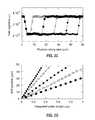
- FIG. 2is directed to an experimental method and corresponding results for domain wall velocity measurements, in which:
- FIG. 2Ashows an optical microscopy image of a typical device including a 50 micrometer long, 2 micrometer wide wire connected on each end to wider regions which are used as bond pads for electrical connections.
- FIG. 2Bpresents Kerr microscopy images showing the position of a domain wall (DW) in response to series of current pulses. Images are saved at regular intervals chosen such that the DW moves by a measurable amount. The two sequences of images shown in this figure are obtained for two opposite current polarities in a 2 micrometer wide wire made out of 20 TaN/15 Pt/3 Co/7 Ni/1.5 Co/50 TaN (all thicknesses herein are in ⁇ unless otherwise specified). Note that the contrast (white or black) is determined by the magnetization direction of the domain which expands as a result of the motion of the DW.
- FIG. 2Cpresents line scans along the wire showing the variation of the Kerr contrast for different positions of the DW. The DW position is measured from these line scans.
- FIG. 2Dshows DW position versus integrated current pulse length t CP for current pulses of various amplitudes. Solid lines show linear fits whose slopes are used to determine the velocity of the DW.
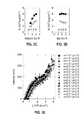
- FIG. 3is directed to current-driven DW motion in Pt/Co/Ni/Co/TaN wires, in which:
- FIG. 3Ashows the DW velocity of a device made out of 20 TaN/15 Pt/3 Co/7 Ni/1.5 Co/50 TaN as a function of the current density in response to 5, 50, and 100 ns long current pulses.
- FIG. 3Bshows critical current density J C (the current density above which current driven DW motion is observed) versus current pulse length, for the same device used in FIG. 3A .
- FIG. 3Dshows PMA constants derived from SQUID magnetometry for films made out of 20 TaN/15 Pt/1.5 Co/7 Ni/y Co/50 TaN. The data are presented as a function of the thickness y of the top Co layer.
- FIG. 3Eshows DW velocity as a function of the current density for 16 different devices made out of 20 TaN/15 Pt/x Co/7 Ni/y Co/50 TaN. Data are only shown for positive current and 5 ns long pulses for clarity.
- FIG. 3Fpresents critical and nucleation current densities J C and J N for devices made out of 20 TaN/15 Pt/x Co/7 Ni/1.5 Co/50 TaN, as a function of the bottom Co layer thickness x for a 50 ns long pulse.
- FIG. 3Gpresents PMA constants for devices made out of 20 TaN/z Pt/3 Co/7 Ni/1.5 Co/50 TaN as a function of the Pt thickness, for devices having no Pt layer on the top.
- FIG. 3Hpresents PMA constants for devices made out of 20 TaN/15 Pt/3 Co/7 Ni/1.5 Co/z Pt/50 TaN as a function of the top Pt thickness z for devices having a 15 ⁇ thick bottom Pt layer.
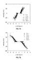
- FIG. 4is directed to DW motion as a function of the number of periods of [Co/Ni] and the thickness of a Pt layer on the top of the stack, with DW velocities being measured for 20 TaN/15 Pt/3 Co/[7 Ni/1.5 Co] N /z Pt/50 TaN, where N is the number of Co/Ni periods and z the thickness of the top Pt layer.
- FIGS. 4E-Gshow DW velocity versus current density for devices made out of 20 TaN/15 Pt/1.5 Co/7 Ni/x Co/10 Pt/y Co/7 Ni/1.5 Co/50 TaN. Current pulse lengths are between 5 and 100 ns.
- FIG. 5is directed to DW motion for different underlayers, in which:
- FIGS. 5A-Cshow DW velocity of devices made out of 50 Ta/50 M/3 Co/7 Ni/1.5 Co/50 TaN as a function of the current density for pulses lengths between 5 and 100 ns and for different metallic underlayers M: Pd ( FIG. 5A ), Ir ( FIG. 5B ), and Au ( FIG. 5C ).
- FIGS. 5D-Ishow DW velocity of devices made out of 50 Ta/(15-z) Au/z Pt/3 Co/7 Ni/1.5 Co/50 TaN as a function of the current density for pulses lengths between 5 and 100 ns.
- FIG. 6is directed to the influence of the induced moment in Pt at the Pt/Co interface, in which:
- FIG. 6Ashows DW velocity versus current density for devices made out of 50 Ta/(15-x) Pt/x Au/3 Co/7 Ni/1.5 Co/50 TaN for 10 ns long current pulses.
- a thin layer of Au of thickness x between 0.25 and 2is inserted at the Pt/Co interface.
- the DW velocitydecreases linearly with x and it extrapolates to 0 for x ⁇ 3 ⁇ .
- FIG. 7is directed to fine control of the DW motion direction by stack engineering.
- the DW velocitywas investigated for devices made out of 50 Ta/10 Au/5 Pt/x Co/7 Ni/y Co/20 Pt/50 TaN, as a function of the current density for pulse lengths between 5 and 100 ns.
- the thicknesses of the top and bottom Pt layersare chosen such that their effects almost compensate each other, leading to a strong sensitivity of the current direction on the thickness of the magnetic layers.
- FIG. 1The preferred embodiment of this invention is shown in FIG. 1 .
- An underlayer 100is first deposited on a substrate.
- intermediate layers 110are deposited on the underlayer.
- An overlayer 120is deposited on top of the intermediate layers.
- the underlayer, intermediate layers and the overlayerform the magnetic wire within which magnetic domains are introduced.
- the intermediate layersare formed from a series of layers that include ferromagnetic and/or ferrimagnetic layers.
- the intermediate layersinclude a sequence of ferromagnetic layers of Co and ferromagnetic layers of Ni and non-ferromagnetic layers of Pt.
- the Pt layersare preferably in contact with a Co layer and a Ni layer. As illustrated in FIG.
- the intermediate layers in the preferred embodimentare formed from layers of Co, Ni, Pt, Co, Ni, Pt and Co deposited successively one after the other.
- Two magnetic domainsare illustrated in FIG. 1 whose magnetization is oriented perpendicular to the interfaces between the Co and Ni layers. In one of the domains the magnetization is oriented with a direction from the underlayer to the overlayer, and in the other domain the magnetization is oriented antiparallel to that of the first domain with a magnetization pointing in a direction from the overlayer to the underlayer. The direction of the magnetization of these domains is illustrated in FIG. 1 by the black arrows. Also shown in FIG.
- 140 ais a region 140 a in the underlayer 140 which exhibits a magnetic moment induced by proximity to the adjacent Co layer.
- 140 bis a region in the overlayer that becomes magnetic due to its proximity to the adjacent Co layer.
- the domain walls and/or their corresponding domainsrepresent data (information) that may be written into, and/or read out of, the wires using one or more devices integrated into the wire.
- PMAperpendicular magnetic anisotropy
- Si wafers coated by a 25 nm thick SiO 2 layerare deposited by magnetron sputtering on Si wafers coated by a 25 nm thick SiO 2 layer.
- SQUID magnetometry and magneto-optical Kerr microscopyare used to measure the magnetic properties of the films.
- Three main figures of meritcan be used to assess the samples: the squareness of the hysteresis loop, the value of the coercive field, and the domain structure during magnetization reversal in an external magnetic field.
- Square hysteresis loopsguarantee that the magnetization is fully saturated in the perpendicular direction at remanence.
- Small values of the coercive fieldare indicative of low pinning leading to small DW propagation fields.
- the Co and Ni layershave an fcc structure and are oriented in the (111) direction.
- the optical microscopy image of a typical deviceis shown in FIG. 2A .
- the wire in the central portion of FIG. 2Awhere DW motion was imaged, is 20 to 50 ⁇ m long. This wire is connected at both ends to wider regions that are used as bond pads for electrical connections. In most cases, we find that the PMA is significantly reduced at the wire bonds, such that DWs are nucleated near the bonds and can propagate in the wire under an external field. Once a single DW is injected in the wire, the field is reduced to zero and DW motion is studied by applying a series of current pulses of length t P to the device.
- Kerr microscopy in differential modeis used to monitor the position of the DW in response to series of current pulses. Images are saved at regular intervals chosen such that the DW moves by a measurable amount between these stored images. Examples of two sequences of images for two different current polarities are shown in FIG. 2B for a 2 ⁇ m wide wire made out of 20 TaN/15 Pt/3 Co/7 Ni/1.5 Co/50 TaN (once again, all thicknesses are in ⁇ ). The current pulses used here were 25 ns long, and the associated currents had a density of ⁇ 1.8 10 8 A/cm 2 . Note that the contrast (white or black) is determined by the magnetization direction of the domain that expands as a result of the motion of the DW.
- the DW positionis determined from the images by automated analysis of the Kerr contrast along the wire ( FIG. 2C ); the profiles shown in this figure are exemplary and are taken for a current density of +1.6 10 8 A/cm 2 and various values of t CP , which is the product of t p and the number of pulses applied to the device.
- the DW velocityis then determined by assuming that the DW moves only during the current pulses. We use a linear fit of the DW position versus the integrated current pulse length t CP ( FIG. 2D ).
- FIG. 2CThe DW position is determined from the images by automated analysis of the Kerr contrast along the wire ( FIG. 2C ); the profiles shown in this figure are exemplary and are taken for a current density of +1.6 10 8 A/cm 2 and various values of t CP , which is the product of t p and the number of pulses applied to the device.
- the DW velocityis then determined by assuming that the DW moves only during the current pulses.
- FIG. 3shows results measured on devices made out of a single Co/Ni/Co stack deposited on Pt.
- the composition of the stackis 20 TaN/15 Pt/x Co/7 Ni/y Co/50 TaN, where the thickness of the two Co layers x and y is varied between 1.5 and 3 ⁇ by 0.5 ⁇ steps.
- the current density Jis calculated from the device resistance by assuming uniform conduction in the metallic layers, which in this case have a total thickness of 26.5 ⁇ .
- DWsmove along the current flow when the current density exceeds a threshold value J C which decreases with t P ( FIG. 3B ).
- J Cwhich decreases with t P
- the DW dynamicsdoes not depend on the orientation of the magnetic domains: both up/down and down/up DWs move in the same direction, at the same velocity.
- the maximum current density that can be achieved for reliable DW motionalso depends on t P .
- a nucleation threshold J NDW motion is replaced by random nucleation of DWs presumably due to Joule heating and magnetization reversal induced by the Oersted field from the current.
- the DW wall velocityis almost independent of t P .
- data for all three values of t P shown in FIG. 3Afall on the same master curve. Similar behavior is also observed for devices having markedly different magnetic properties.
- the PMA constant K of the samplescan be changed systematically by varying the thickness x of the bottom Co layer adjacent to Pt.
- the PMA constant Kis strongly dependent on the thickness of the Pt underlayer deposited below the Co/Ni/Co trilayer. As shown in FIG. 3G , K increases linearly for Pt thicknesses up to ⁇ 20 ⁇ , above which it progressively saturates toward a value exceeding 7.2 10 6 erg/cm 3 . On the other hand, the PMA is weakly dependent on the thickness of the Pt overlayer deposited above the Co/Ni/Co trilayer ( FIG. 3H ). These results clearly show that the Pt/Co and Co/Pt interfaces have significant differences which lead to very different effects on the magnetic properties of the multilayer.
- the DW velocityis determined by the difference between the numbers of Pt/Co and Co/Pt interfaces.
- the DW velocityis very high ( ⁇ 130 m/s).
- FIG. 4Fthere is one Pt/Co and one Co/Pt interface, and the DW velocity is strongly reduced down to ⁇ 30 m/s.
- FIG. 4Gin which there are 2 Pt/Co interfaces but also one Co/Pt interface, the DW velocity reaches an intermediate value between the 2 previous examples ( ⁇ 90 m/s).
- the DW velocitydrops to almost zero while J c increases by one order of magnitude, indicating that the influence of the Au and Pt layers almost cancel each other.
- J cdecreases for x>6 up to 15 ⁇ , but the dependence is much weaker.
- this critical thicknessis smaller than the spin diffusion length of Pt, but corresponds to the typical length over which significant magnetic moments are induced in Pt (2 to 4 atomic layers).
- the induced magnetic momentis largely parallel to that of the magnetic layers.
- a significant componentmay be parallel to the interface because of the Dzyaloshinskii-Moriya interaction at the Pt/Co interface.
- the structure of the filmsis 50 Ta/(15-x) Pt/x Au/3 Co/7 Ni/1.5 Co/50 TaN.
- the DW velocity versus current densityis shown in FIG. 6A for x between 0.25 and 2 for 10 ns long current pulses. Motion is along the current flow for all values of x, but the DW velocity is reduced significantly for increasing x. Note that J C is almost independent of x, whereas J N decreases with x as a result of the smaller PMA.
Landscapes
- Engineering & Computer Science (AREA)
- Computer Hardware Design (AREA)
- Hall/Mr Elements (AREA)
- Thin Magnetic Films (AREA)
Abstract
Description
Claims (28)
Priority Applications (3)
| Application Number | Priority Date | Filing Date | Title |
|---|---|---|---|
| US13/543,061US8638601B1 (en) | 2012-07-06 | 2012-07-06 | Domain wall motion in perpendicularly magnetized wires having magnetic multilayers with engineered interfaces |
| PCT/EP2013/061367WO2014005772A1 (en) | 2012-07-06 | 2013-06-03 | Domain wall motion in perpendicularly magnetized wires having magnetic multilayers with engineered interfaces |
| CN201380027755.4ACN104321823B (en) | 2012-07-06 | 2013-06-03 | Domain wall motion in there is the perpendicular magnetization line of magnetic multiplayer at band engineering design interface |
Applications Claiming Priority (1)
| Application Number | Priority Date | Filing Date | Title |
|---|---|---|---|
| US13/543,061US8638601B1 (en) | 2012-07-06 | 2012-07-06 | Domain wall motion in perpendicularly magnetized wires having magnetic multilayers with engineered interfaces |
Publications (2)
| Publication Number | Publication Date |
|---|---|
| US20140009993A1 US20140009993A1 (en) | 2014-01-09 |
| US8638601B1true US8638601B1 (en) | 2014-01-28 |
Family
ID=48607225
Family Applications (1)
| Application Number | Title | Priority Date | Filing Date |
|---|---|---|---|
| US13/543,061ActiveUS8638601B1 (en) | 2012-07-06 | 2012-07-06 | Domain wall motion in perpendicularly magnetized wires having magnetic multilayers with engineered interfaces |
Country Status (2)
| Country | Link |
|---|---|
| US (1) | US8638601B1 (en) |
| WO (1) | WO2014005772A1 (en) |
Cited By (2)
| Publication number | Priority date | Publication date | Assignee | Title |
|---|---|---|---|---|
| US10755759B2 (en) | 2018-06-28 | 2020-08-25 | International Business Machines Corporation | Symmetrically programmable resistive synapse for RPU using current-programmed single domain wall ferroelectric |
| US20230180624A1 (en)* | 2021-12-07 | 2023-06-08 | Samsung Electronics Co., Ltd. | Magnetic tunnel junction including hexagonal multi-layered structure |
Families Citing this family (4)
| Publication number | Priority date | Publication date | Assignee | Title |
|---|---|---|---|---|
| CN106855812A (en)* | 2015-12-08 | 2017-06-16 | 北京三星通信技术研究有限公司 | The method and apparatus for configuring user terminal |
| EP3916728A1 (en) | 2020-05-26 | 2021-12-01 | Max-Planck-Gesellschaft zur Förderung der Wissenschaften e.V. | Increased efficiency of current induced motion of chiral domain walls by interface engineering |
| EP4009324A1 (en) | 2020-12-03 | 2022-06-08 | Max-Planck-Gesellschaft zur Förderung der Wissenschaften e.V. | Antiskyrmions and elliptical skyrmions in nano-stripes |
| EP4270507A1 (en) | 2022-04-25 | 2023-11-01 | Max-Planck-Gesellschaft zur Förderung der Wissenschaften e.V. | Energy efficient non-volatile cryogenic memory - supertrack |
Citations (26)
| Publication number | Priority date | Publication date | Assignee | Title |
|---|---|---|---|---|
| US20040251232A1 (en)* | 2003-06-10 | 2004-12-16 | International Business Machines Corporation | Method of fabricating a shiftable magnetic shift register |
| US6834005B1 (en) | 2003-06-10 | 2004-12-21 | International Business Machines Corporation | Shiftable magnetic shift register and method of using the same |
| US6898132B2 (en) | 2003-06-10 | 2005-05-24 | International Business Machines Corporation | System and method for writing to a magnetic shift register |
| US6920062B2 (en) | 2003-10-14 | 2005-07-19 | International Business Machines Corporation | System and method for reading data stored on a magnetic shift register |
| EP1701357A1 (en) | 2005-03-09 | 2006-09-13 | Korea University Foundation | Magnetic tunnel junction structure with amorphous CoFeSiB or NiFeSiB free layer |
| WO2007063718A1 (en) | 2005-11-30 | 2007-06-07 | Renesas Technology Corp. | Nonvolatile memory device |
| US20080025060A1 (en)* | 2006-07-25 | 2008-01-31 | Samsung Electronics Co., Ltd. | Semiconductor device using magnetic domain wall moving |
| US20080068936A1 (en)* | 2006-09-15 | 2008-03-20 | Samsung Electronics Co., Ltd | Data writing and reading method for memory device employing magnetic domain wall movement |
| US20080137405A1 (en) | 2004-01-15 | 2008-06-12 | Japan Science And Technology Agency | Current Injection Magnetic Domain Wall Moving Element |
| US20080138661A1 (en)* | 2006-12-06 | 2008-06-12 | Samsung Electronics Co., Ltd. | Information storage device using movement of magnetic domain wall, and methods of manufacturing and operating the information storage device |
| US20080258247A1 (en) | 2007-04-18 | 2008-10-23 | Freescale Semiconductor, Inc. | Spin-transfer mram structure and methods |
| US7551469B1 (en) | 2009-01-05 | 2009-06-23 | Internationa Business Machines Corporation | Unidirectional racetrack memory device |
| US20090168493A1 (en) | 2004-10-26 | 2009-07-02 | Samsung Electronics Co., Ltd | Semiconductor memory device with stacked memory cell and method of manufacturing the stacked memory cell |
| US20090185312A1 (en)* | 2008-01-21 | 2009-07-23 | Samsung Electronics Co., Ltd. | Information storage devices using magnetic domain wall movement |
| US20090303631A1 (en) | 2008-06-09 | 2009-12-10 | Samsung Electronics Co., Ltd. | Magnetic racetrack memory device including write-back loop |
| US7652906B2 (en)* | 2006-09-15 | 2010-01-26 | Samsung Electronics Co., Ltd. | Memory device employing magnetic domain wall movement |
| WO2010020440A1 (en) | 2008-08-22 | 2010-02-25 | International Business Machines Corporation | Magnetic racetrack memory device |
| US20100061135A1 (en) | 2008-09-10 | 2010-03-11 | Fujitsu Limited | Magnetic wire unit and storage device |
| US20100085659A1 (en)* | 2008-10-08 | 2010-04-08 | Samsung Electronics Co., Ltd. | Information storage devices using magnetic domain wall motion |
| US20100118583A1 (en) | 2008-11-12 | 2010-05-13 | Industrial Technology Research Institute | Magetic shift register and data accessing method |
| US20100128510A1 (en) | 2008-11-13 | 2010-05-27 | Ingenia Holdings (Uk) Limited | Magnetic Data Storage |
| US20100148288A1 (en) | 2008-11-19 | 2010-06-17 | Johnson Mark B | Vertical Cell Edge Junction Magnetoelectronic Device Family |
| US7876595B2 (en)* | 2008-09-19 | 2011-01-25 | Seagate Technology Llc | Magnetic shift register as counter and data storage device |
| US20110163402A1 (en) | 2008-09-02 | 2011-07-07 | Shunsuke Fukami | Magnetic memory and method of manufacturing the same |
| US20110170342A1 (en) | 2008-10-08 | 2011-07-14 | Seagate Technology Llc | Electronic devices utilizing spin torque transfer to flip magnetic orientation |
| US20120250398A1 (en)* | 2011-03-28 | 2012-10-04 | Kabushiki Kaisha Toshiba | Magnetic storage element, magnetic storage device, and magnetic memory |
- 2012
- 2012-07-06USUS13/543,061patent/US8638601B1/enactiveActive
- 2013
- 2013-06-03WOPCT/EP2013/061367patent/WO2014005772A1/enactiveApplication Filing
Patent Citations (34)
| Publication number | Priority date | Publication date | Assignee | Title |
|---|---|---|---|---|
| US6834005B1 (en) | 2003-06-10 | 2004-12-21 | International Business Machines Corporation | Shiftable magnetic shift register and method of using the same |
| US6898132B2 (en) | 2003-06-10 | 2005-05-24 | International Business Machines Corporation | System and method for writing to a magnetic shift register |
| US7108797B2 (en)* | 2003-06-10 | 2006-09-19 | International Business Machines Corporation | Method of fabricating a shiftable magnetic shift register |
| US20040251232A1 (en)* | 2003-06-10 | 2004-12-16 | International Business Machines Corporation | Method of fabricating a shiftable magnetic shift register |
| US6920062B2 (en) | 2003-10-14 | 2005-07-19 | International Business Machines Corporation | System and method for reading data stored on a magnetic shift register |
| US20080137405A1 (en) | 2004-01-15 | 2008-06-12 | Japan Science And Technology Agency | Current Injection Magnetic Domain Wall Moving Element |
| US20090168493A1 (en) | 2004-10-26 | 2009-07-02 | Samsung Electronics Co., Ltd | Semiconductor memory device with stacked memory cell and method of manufacturing the stacked memory cell |
| EP1701357A1 (en) | 2005-03-09 | 2006-09-13 | Korea University Foundation | Magnetic tunnel junction structure with amorphous CoFeSiB or NiFeSiB free layer |
| WO2007063718A1 (en) | 2005-11-30 | 2007-06-07 | Renesas Technology Corp. | Nonvolatile memory device |
| US20080025060A1 (en)* | 2006-07-25 | 2008-01-31 | Samsung Electronics Co., Ltd. | Semiconductor device using magnetic domain wall moving |
| US7710756B2 (en)* | 2006-07-25 | 2010-05-04 | Samsung Electronics Co., Ltd. | Semiconductor device using magnetic domain wall moving |
| US7652906B2 (en)* | 2006-09-15 | 2010-01-26 | Samsung Electronics Co., Ltd. | Memory device employing magnetic domain wall movement |
| US7751224B2 (en)* | 2006-09-15 | 2010-07-06 | Samsung Electronics Co., Ltd. | Data writing and reading method for memory device employing magnetic domain wall movement |
| US20080068936A1 (en)* | 2006-09-15 | 2008-03-20 | Samsung Electronics Co., Ltd | Data writing and reading method for memory device employing magnetic domain wall movement |
| US7924594B2 (en)* | 2006-09-15 | 2011-04-12 | Samsung Electronics Co., Ltd. | Data writing and reading method for memory device employing magnetic domain wall movement |
| US20100238698A1 (en)* | 2006-09-15 | 2010-09-23 | Chee-Khong Lim | Data writing and reading method for memory device employing magnetic domain wall movement |
| US20080138661A1 (en)* | 2006-12-06 | 2008-06-12 | Samsung Electronics Co., Ltd. | Information storage device using movement of magnetic domain wall, and methods of manufacturing and operating the information storage device |
| US7965470B2 (en)* | 2006-12-06 | 2011-06-21 | Samsung Electronics Co., Ltd. | Information storage device using movement of magnetic domain wall, and methods of manufacturing and operating the information storage device |
| US20080258247A1 (en) | 2007-04-18 | 2008-10-23 | Freescale Semiconductor, Inc. | Spin-transfer mram structure and methods |
| US20090185312A1 (en)* | 2008-01-21 | 2009-07-23 | Samsung Electronics Co., Ltd. | Information storage devices using magnetic domain wall movement |
| US8313847B2 (en)* | 2008-01-21 | 2012-11-20 | Samsung Electronics Co., Ltd. | Information storage devices using magnetic domain wall movement |
| US20090303631A1 (en) | 2008-06-09 | 2009-12-10 | Samsung Electronics Co., Ltd. | Magnetic racetrack memory device including write-back loop |
| US7965468B2 (en) | 2008-06-09 | 2011-06-21 | Samsung Electronics Co., Ltd. | Magnetic racetrack memory device including write-back loop |
| WO2010020440A1 (en) | 2008-08-22 | 2010-02-25 | International Business Machines Corporation | Magnetic racetrack memory device |
| US20110163402A1 (en) | 2008-09-02 | 2011-07-07 | Shunsuke Fukami | Magnetic memory and method of manufacturing the same |
| US20100061135A1 (en) | 2008-09-10 | 2010-03-11 | Fujitsu Limited | Magnetic wire unit and storage device |
| US7876595B2 (en)* | 2008-09-19 | 2011-01-25 | Seagate Technology Llc | Magnetic shift register as counter and data storage device |
| US20100085659A1 (en)* | 2008-10-08 | 2010-04-08 | Samsung Electronics Co., Ltd. | Information storage devices using magnetic domain wall motion |
| US20110170342A1 (en) | 2008-10-08 | 2011-07-14 | Seagate Technology Llc | Electronic devices utilizing spin torque transfer to flip magnetic orientation |
| US20100118583A1 (en) | 2008-11-12 | 2010-05-13 | Industrial Technology Research Institute | Magetic shift register and data accessing method |
| US20100128510A1 (en) | 2008-11-13 | 2010-05-27 | Ingenia Holdings (Uk) Limited | Magnetic Data Storage |
| US20100148288A1 (en) | 2008-11-19 | 2010-06-17 | Johnson Mark B | Vertical Cell Edge Junction Magnetoelectronic Device Family |
| US7551469B1 (en) | 2009-01-05 | 2009-06-23 | Internationa Business Machines Corporation | Unidirectional racetrack memory device |
| US20120250398A1 (en)* | 2011-03-28 | 2012-10-04 | Kabushiki Kaisha Toshiba | Magnetic storage element, magnetic storage device, and magnetic memory |
Non-Patent Citations (14)
| Title |
|---|
| Daalderop et al., "Prediction and Confirmation of Perpendicular Magnetic Anisotropy in Co/Ni Multilayers", Physical Review Letters, vol. 68, No. 5, Feb. 3, 1992, pp. 682-685. |
| Fukami et al., "Low-Current Perpendicular Domain Wall Motion Cell for Scalable High-Speed MRAM", Symposium on VLSI Technology Digest of Technical Papers, 2009, pp. 230-231. |
| Fukami et al., "Stack Structure Dependence of Co/Ni Multilayer for Current-Induced Domain Wall Motion", Applied Physics Express 3, 2010, pp. 113002-1-13002-3. |
| Hayashi et al., "Current-Controlled Magnetic Domain-Wall Nanowire Shift Register", Science, vol. 320, Apr. 11, 2008, pp. 209-211. |
| Lau et al., "Magnetic nanostructures for advanced technologies: fabrication, metrology and challenges", Journal of Physics D: Applied Physics, 44, 303001, 2011, pp. 1-43. |
| Miron et al., "Current-driven spin torque induced by the Rashba effect in a ferromagnetic metal layer", Letters Nature Materials, vol. 9, Mar. 2010, pp. 230-234. |
| Miron et al., "Fast current-induced domain-wall motion controlled by the Rashba effect", Letters Natural Materials, vol. 10, Jun. 2011, pp. 419-423. |
| Parkin et al., "Magnetic Domain-Wall Racetrack Memory", Science, vol. 320, Apr. 11, 2008, pp. 190-194. |
| Parkin, "Racetrack Memory: a storage class memory based on current controlled magnetic domain wall motion", IEEE 978-1-4244-3527, Feb. 2009, pp. 3-6. |
| PCT International Search Report and the Written Opinion, International application No. PCT/EP2013/061367, Jul. 18, 2013. |
| Rodmacq et al., "Influence of thermal annealing on the perpendicular magnetic anisotropy of Pt/Co/AlOx trilayers", Physical Review B 79, 2009, pp. 024423-1-024423-8. |
| Thomas et al., "Racetrack Memory: a high-performance, low-cost, non-volatile memory based on magnetic domain walls", IEEE 978-1-4577-0505, Feb. 2011, pp. 242.1-24.2.4. |
| Weller et al., "Orbital magnetic moments of Co in multilayers with perpendicular magnetic anisotropy", Physical Review, 1994, vol. 49, No. 18, pp. 12888-12896. |
| Wilhelm et al., "Interface magnetism in 3d/5d multilayers probed by X-ray magnetic circular dichroism", Phys. Stat. Sol. (a), 2003, vol. 196, No. 1, pp. 33-36. |
Cited By (2)
| Publication number | Priority date | Publication date | Assignee | Title |
|---|---|---|---|---|
| US10755759B2 (en) | 2018-06-28 | 2020-08-25 | International Business Machines Corporation | Symmetrically programmable resistive synapse for RPU using current-programmed single domain wall ferroelectric |
| US20230180624A1 (en)* | 2021-12-07 | 2023-06-08 | Samsung Electronics Co., Ltd. | Magnetic tunnel junction including hexagonal multi-layered structure |
Also Published As
| Publication number | Publication date |
|---|---|
| US20140009993A1 (en) | 2014-01-09 |
| CN104321823A (en) | 2015-01-28 |
| WO2014005772A1 (en) | 2014-01-09 |
Similar Documents
| Publication | Publication Date | Title |
|---|---|---|
| US8687415B2 (en) | Domain wall motion in perpendicularly magnetized wires having artificial antiferromagnetically coupled multilayers with engineered interfaces | |
| US10854257B2 (en) | Electric field switchable magnetic devices | |
| US9515254B2 (en) | Storage element, memory and electronic apparatus | |
| US9236103B2 (en) | Bipolar spin-transfer switching | |
| US7532502B2 (en) | Spin injection magnetic domain wall displacement device and element thereof | |
| US7532504B2 (en) | Spin injection magnetic domain wall displacement device and element thereof | |
| US7018725B2 (en) | Magneto-resistance effect element magneto-resistance effect memory cell, MRAM, and method for performing information write to or read from the magneto-resistance effect memory cell | |
| US8638601B1 (en) | Domain wall motion in perpendicularly magnetized wires having magnetic multilayers with engineered interfaces | |
| US20160314827A1 (en) | A Memory Device, Comprising at Least One Element and Associated Method Spintronics | |
| JP2005109263A (en) | Magnetic element and magnetic memory | |
| JP2004193595A (en) | Magnetic cell and magnetic memory | |
| JP2001077442A (en) | Memory element | |
| JP7614589B2 (en) | Spin injection source, magnetic memory, spin Hall oscillator, and computer | |
| WO2012068309A2 (en) | Bipolar spin-transfer switching | |
| CN108738371B (en) | Magnetization reversal element, magnetoresistive effect element, and memory device | |
| JP2007080952A (en) | Multilevel recording spin injection magnetization reversal element and apparatus using the same | |
| JP3547974B2 (en) | Magnetic element, magnetic head and magnetic storage device using the same | |
| Inomata | Giant magnetoresistance and its sensor applications | |
| US20120063217A1 (en) | Memory element and memory device | |
| Cartier et al. | Magnetic domain configurations in exchange-coupled NiO/Co bilayer films | |
| JP2007281334A (en) | Spin injection magnetization reversal element, manufacturing method thereof, and magnetic recording apparatus using the same | |
| CN104321823B (en) | Domain wall motion in there is the perpendicular magnetization line of magnetic multiplayer at band engineering design interface | |
| JPH10308313A (en) | Magnetic element, magnetic head and magnetic storage device using the same | |
| JP7300666B2 (en) | magnetic memory element | |
| Wilhelm | Influence of the local grain structure on the magnetization reversal behavior of ferromagnetic Co/Pt nanodots |
Legal Events
| Date | Code | Title | Description |
|---|---|---|---|
| AS | Assignment | Owner name:INTERNATIONAL BUSINESS MACHINES CORPORATION, NEW Y Free format text:ASSIGNMENT OF ASSIGNORS INTEREST;ASSIGNORS:PARKIN, STUART STEPHEN PAPWORTH;THOMAS, LUC;YANG, SEE-HUN;REEL/FRAME:028501/0632 Effective date:20120706 | |
| AS | Assignment | Owner name:INTERNATIONAL BUSINESS MACHINES CORPORATION, NEW Y Free format text:CORRECTIVE ASSIGNMENT TO CORRECT THE ERRONEOUS INVENTOR EXECUTION DATE LISTED FOR INVENTOR LUC THOMAS ON THE ORIGINAL COVER SHEET PREVIOUSLY RECORDED ON REEL 028501 FRAME 0632. ASSIGNOR(S) HEREBY CONFIRMS THE ASSIGNMENT OF ASSIGNORS INTEREST;ASSIGNORS:PARKIN, STUART STEPHEN PAPWORTH;THOMAS, LUC;YANG, SEE-HUN;SIGNING DATES FROM 20120705 TO 20120706;REEL/FRAME:028546/0661 | |
| STCF | Information on status: patent grant | Free format text:PATENTED CASE | |
| AS | Assignment | Owner name:GLOBALFOUNDRIES U.S. 2 LLC, NEW YORK Free format text:ASSIGNMENT OF ASSIGNORS INTEREST;ASSIGNOR:INTERNATIONAL BUSINESS MACHINES CORPORATION;REEL/FRAME:036550/0001 Effective date:20150629 | |
| AS | Assignment | Owner name:GLOBALFOUNDRIES INC., CAYMAN ISLANDS Free format text:ASSIGNMENT OF ASSIGNORS INTEREST;ASSIGNORS:GLOBALFOUNDRIES U.S. 2 LLC;GLOBALFOUNDRIES U.S. INC.;REEL/FRAME:036779/0001 Effective date:20150910 | |
| FPAY | Fee payment | Year of fee payment:4 | |
| AS | Assignment | Owner name:WILMINGTON TRUST, NATIONAL ASSOCIATION, DELAWARE Free format text:SECURITY AGREEMENT;ASSIGNOR:GLOBALFOUNDRIES INC.;REEL/FRAME:049490/0001 Effective date:20181127 | |
| AS | Assignment | Owner name:GLOBALFOUNDRIES U.S. INC., CALIFORNIA Free format text:ASSIGNMENT OF ASSIGNORS INTEREST;ASSIGNOR:GLOBALFOUNDRIES INC.;REEL/FRAME:054633/0001 Effective date:20201022 | |
| AS | Assignment | Owner name:GLOBALFOUNDRIES INC., CAYMAN ISLANDS Free format text:RELEASE BY SECURED PARTY;ASSIGNOR:WILMINGTON TRUST, NATIONAL ASSOCIATION;REEL/FRAME:054636/0001 Effective date:20201117 | |
| AS | Assignment | Owner name:GLOBALFOUNDRIES U.S. INC., NEW YORK Free format text:RELEASE BY SECURED PARTY;ASSIGNOR:WILMINGTON TRUST, NATIONAL ASSOCIATION;REEL/FRAME:056987/0001 Effective date:20201117 | |
| MAFP | Maintenance fee payment | Free format text:PAYMENT OF MAINTENANCE FEE, 8TH YEAR, LARGE ENTITY (ORIGINAL EVENT CODE: M1552); ENTITY STATUS OF PATENT OWNER: LARGE ENTITY Year of fee payment:8 | |
| FEPP | Fee payment procedure | Free format text:MAINTENANCE FEE REMINDER MAILED (ORIGINAL EVENT CODE: REM.); ENTITY STATUS OF PATENT OWNER: LARGE ENTITY |