US8638320B2 - Stylus orientation detection - Google Patents
Stylus orientation detectionDownload PDFInfo
- Publication number
- US8638320B2 US8638320B2US13/166,743US201113166743AUS8638320B2US 8638320 B2US8638320 B2US 8638320B2US 201113166743 AUS201113166743 AUS 201113166743AUS 8638320 B2US8638320 B2US 8638320B2
- Authority
- US
- United States
- Prior art keywords
- orientation
- capacitance
- stylus
- electrode
- image
- Prior art date
- Legal status (The legal status is an assumption and is not a legal conclusion. Google has not performed a legal analysis and makes no representation as to the accuracy of the status listed.)
- Active, expires
Links
Images


Classifications
- G—PHYSICS
- G06—COMPUTING OR CALCULATING; COUNTING
- G06F—ELECTRIC DIGITAL DATA PROCESSING
- G06F3/00—Input arrangements for transferring data to be processed into a form capable of being handled by the computer; Output arrangements for transferring data from processing unit to output unit, e.g. interface arrangements
- G06F3/01—Input arrangements or combined input and output arrangements for interaction between user and computer
- G06F3/03—Arrangements for converting the position or the displacement of a member into a coded form
- G06F3/033—Pointing devices displaced or positioned by the user, e.g. mice, trackballs, pens or joysticks; Accessories therefor
- G06F3/0354—Pointing devices displaced or positioned by the user, e.g. mice, trackballs, pens or joysticks; Accessories therefor with detection of 2D relative movements between the device, or an operating part thereof, and a plane or surface, e.g. 2D mice, trackballs, pens or pucks
- G06F3/03545—Pens or stylus
- G—PHYSICS
- G06—COMPUTING OR CALCULATING; COUNTING
- G06F—ELECTRIC DIGITAL DATA PROCESSING
- G06F3/00—Input arrangements for transferring data to be processed into a form capable of being handled by the computer; Output arrangements for transferring data from processing unit to output unit, e.g. interface arrangements
- G06F3/01—Input arrangements or combined input and output arrangements for interaction between user and computer
- G06F3/03—Arrangements for converting the position or the displacement of a member into a coded form
- G06F3/041—Digitisers, e.g. for touch screens or touch pads, characterised by the transducing means
- G06F3/044—Digitisers, e.g. for touch screens or touch pads, characterised by the transducing means by capacitive means
- G06F3/0441—Digitisers, e.g. for touch screens or touch pads, characterised by the transducing means by capacitive means using active external devices, e.g. active pens, for receiving changes in electrical potential transmitted by the digitiser, e.g. tablet driving signals
- G—PHYSICS
- G06—COMPUTING OR CALCULATING; COUNTING
- G06F—ELECTRIC DIGITAL DATA PROCESSING
- G06F3/00—Input arrangements for transferring data to be processed into a form capable of being handled by the computer; Output arrangements for transferring data from processing unit to output unit, e.g. interface arrangements
- G06F3/01—Input arrangements or combined input and output arrangements for interaction between user and computer
- G06F3/03—Arrangements for converting the position or the displacement of a member into a coded form
- G06F3/041—Digitisers, e.g. for touch screens or touch pads, characterised by the transducing means
- G06F3/044—Digitisers, e.g. for touch screens or touch pads, characterised by the transducing means by capacitive means
- G06F3/0442—Digitisers, e.g. for touch screens or touch pads, characterised by the transducing means by capacitive means using active external devices, e.g. active pens, for transmitting changes in electrical potential to be received by the digitiser
Definitions
- Thisrelates generally to touch sensing and more particularly, to providing a stylus for use with a touch sensitive device and detecting an orientation of the stylus relative to the device.
- Touch sensitive devicescan include a touch sensor panel, which can be a clear panel with a touch sensitive surface, and a display device such as a liquid crystal display (LCD) that can be positioned partially or fully behind the panel, or integrated with the panel, so that the touch sensitive surface can substantially cover the viewable area of the display device.
- a touch sensor panelwhich can be a clear panel with a touch sensitive surface
- a display devicesuch as a liquid crystal display (LCD) that can be positioned partially or fully behind the panel, or integrated with the panel, so that the touch sensitive surface can substantially cover the viewable area of the display device.
- LCDliquid crystal display
- Touch sensitive devicescan generally allow a user to perform various functions by touching or hovering over the touch sensor panel using one or more fingers, a stylus or other object at a location often dictated by a user interface (UI) including virtual buttons, keys, bars, displays, and other elements, being displayed by the display device.
- UIuser interface
- touch screenscan recognize a touch event and the position of the touch event on the touch sensor panel or a hover event and the position of the hover event on the touch sensor panel, and the computing system can then interpret the touch or hover event in accordance with the display appearing at the time of the event, and thereafter can perform one or more operations based on the event.
- the stylusWhen a stylus has been used as an input device, the stylus has traditionally provided simply a touch input without additional information that can be helpful to the touch sensitive device for detecting touch or hover events.
- Thisrelates to detection of an orientation of a stylus relative to a surface.
- the orientation of a stylus relative to a contacting surfacee.g., a touch panel
- the orientation of a stylus relative to a contacting surfacecan be detected by first detecting the orientation of the stylus relative to a reference, detecting the orientation of the contacting surface relative to the reference, and then calculating the orientation of the stylus relative to the contacting surface using the two detected orientations.
- Stylus orientationcan advantageously be used to affect width and darkness of a resultant line displayed on the touch panel, thereby improving the realism of the stylus experience.
- the styluscan advantageously be used to improve touch and hover sensing and to preserve power savings in the contacting device.
- FIG. 1illustrates an exemplary stylus for use with a touch panel according to various embodiments.
- FIGS. 2 a and 2 billustrate a side view and a bottom view respectively of an exemplary stylus according to various embodiments.
- FIG. 3illustrates a cross-sectional view of an exemplary stylus according to various embodiments.
- FIGS. 4 a and 4 billustrates a perpendicular orientation and a tilted orientation respectively of an exemplary stylus according to various embodiments.
- FIG. 5illustrates an exemplary method for detecting an orientation of a stylus according to various embodiments.
- FIGS. 6 a and 6 billustrate a side view and a bottom view respectively of another exemplary stylus according to various embodiments.
- FIGS. 7 a , 7 b , and 7 cillustrate a perpendicular orientation, a tilted orientation, and a rotated-tilted orientation respectively of an exemplary stylus according to various embodiments.
- FIG. 8illustrates another exemplary method for detecting an orientation of a stylus according to various embodiments.
- FIG. 9illustrates an exemplary stylus having an orientation sensor for use with a touch panel also having an orientation sensor according to various embodiments.
- FIG. 10illustrates another exemplary method for detecting an orientation of a stylus according to various embodiments.
- FIG. 11illustrates an exemplary stylus tip having strip electrodes according to various embodiments.
- FIG. 12illustrates an exemplary stylus tip having a wide ring electrode according to various embodiments.
- FIG. 13illustrates an exemplary flat stylus tip according to various embodiments.
- FIGS. 14 a and 14 billustrate a side view and a bottom view respectively of another exemplary stylus according to various embodiments.
- FIGS. 15 a and 15 billustrate a perpendicular orientation and a tilted orientation respectively of an exemplary stylus according to various embodiments.
- FIG. 16illustrates another exemplary method for detecting an orientation of a stylus according to various embodiments.
- FIG. 17illustrates exemplary drive circuitry for a stylus according to various embodiments.
- FIG. 18illustrates exemplary sense circuitry for a stylus according to various embodiments.
- FIG. 19illustrates an exemplary computing system for use with a stylus according to various embodiments.
- FIG. 20illustrates an exemplary mobile telephone for use with a stylus according to various embodiments.
- FIG. 21illustrates an exemplary digital media player for use with a stylus according to various embodiments.
- FIG. 22illustrates an exemplary personal computer for use with a stylus according to various embodiments.
- the orientation of a stylus relative to a contacting surfacee.g., a touch panel
- the orientation of a stylus relative to a contacting surfacecan be detected by detecting a capacitance at one or more locations on the stylus relative to the surface, and then using the capacitance(s) to determine the orientation of the stylus relative to the surface.
- the orientation of a stylus relative to a contacting surfacee.g., a touch panel
- Stylus orientationcan advantageously be used to affect width and darkness of a resultant line displayed on the touch panel, thereby improving the realism of the stylus experience.
- the styluscan advantageously be used to improve touch and hover sensing and to preserve power savings in the contacting device.
- touch panelAlthough some embodiments are described herein in terms of a touch panel, it is to be understood that other touch sensitive devices capable of sensing an object touching or hovering over the devices can be used according to various embodiments.
- FIG. 1illustrates an exemplary stylus for use with a touch panel according to various embodiments.
- touch panel 120can include an array of pixels 106 formed at the crossing points of conductive rows 101 and columns 102 .
- FIG. 1depicts the conductive elements 101 , 102 in rows and columns, other configurations of conductive elements are also possible according to various embodiments.
- the stylusWhen stylus 110 touches or hovers over a surface of the touch panel 120 , the stylus can form a capacitance with one or more of the conductive rows 101 and/or columns 102 that can be detected by sensing circuitry (not shown).
- the stylus touch or hovercan be represented in an image captured at the touch panel 120 and processed for input information regarding the stylus 110 .
- the stylus 110can act as a driving element stimulated by a stimulation signal to capacitively couple with a proximate conductive row 101 or column 102 of the touch panel 120 , thereby forming a capacitive path for coupling charge from the stylus to that proximate row or column.
- the proximate row 101 or column 102can output signals representative of the coupling charge to the sensing circuitry.
- the stylus 110can act as a sensing element capacitively coupled with a proximate conductive row 101 or column 102 of the touch panel 120 that has been stimulated by a stimulation signal. The stylus 110 can then output signals representative of the coupling charge to the sensing circuitry.
- FIG. 2 aillustrates a side view of an exemplary stylus according to various embodiments.
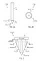
- stylus 210can include shaft 218 and tip 212 .
- the tip 212can include electrode 214 at the distal end of the tip for contacting a surface and electrode 216 proximate to the distal end and forming a ring around the tip.
- the electrodes 214 , 216can be any suitable conductive material, such as metal, paint, ink, and the like.
- the tipcan be replaceable.
- the shaft 218can similarly be any suitable conductive material or any suitable insulating material, depending on the requirements of the stylus 210 .
- the shaft 218can house stylus circuitry, e.g., signal transmitting and receiving elements, signal processing elements, and the like, depending on the requirements of the stylus 210 .
- FIG. 2 billustrates a bottom view of the exemplary stylus of FIG. 2 a according to various embodiments.
- stylus 210can have a conical shaped tip 212 with electrode 214 at the distal end of the tip and electrode 216 proximate to the distal end and forming a ring around the tip.
- FIG. 3illustrates a cross-sectional view of the exemplary stylus of FIGS. 2 a and 2 b .
- tip 212 of stylus 210can have electrode 214 that forms a distal end of the tip, with the distal end portion exposed to contact a surface and another portion of the electrode extended within the tip.
- the tip 212can also have electrode 216 that forms a ring around the tip, with a portion of the electrode exposed on the outer surface of the tip and another portion of the electrode extended within the tip.
- Insulator 315can separate the electrodes 214 , 216 and cover the extended portion of the ring electrode 216 .
- the electrodes 214 , 216can electrically couple to circuit board 380 or other stylus circuitry for transmitting and receiving signals through connections 378 , for example.
- a styluscan have various orientations as it touches or hovers over a touch panel.
- a particular action of the touch panelcan be performed based on the stylus orientation. Accordingly, detecting the stylus orientation can be helpful in touch panel operation.
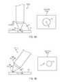
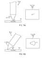
- FIGS. 4 a and 4 billustrate various orientations of the exemplary stylus of FIGS. 2 a and 2 b as it touches a touch panel according to various embodiments.
- stylus 410can have a perpendicular orientation as it touches touch panel 420 .
- tip electrode 414can form capacitance C 1 with a proximate conductive element, e.g., row(s) and/or column(s), (not shown) of the panel.
- ring electrode 416can form capacitance C 2 with a proximate conductive element, e.g., row(s) and/or column(s), of the panel 420 .
- Image 430 captured at the panel 420can show touch or hover images resulting from the two capacitances C 1 , C 2 . Because the stylus 410 is perpendicular to the panel 420 , the image 430 can show the tip capacitance C 1 image surrounded by the ring capacitance C 2 image.
- the stylus 410can have a tilted orientation as it touches the panel 420 .
- the image 430 captured at the panel 420can show a shift in the positions of the touch or hover images resulting from two capacitances C 1 , C 2 relative to each other.
- the ring capacitance C 2 imagehas shifted to the right of the tip capacitance C 1 image.
- the amount of the shiftcan be a function of the amount of stylus tilt. For example, the greater the tilt, the further the ring capacitance C 2 image is from the tip capacitance C 1 image. Conversely, the lesser the tilt, the closer the ring capacitance C 2 image is and/or overlaps the tip capacitance C 1 image. Therefore, by determining the proximity of the two capacitances C 1 , C 2 images in the captured image, the amount of stylus tilt can be determined.
- the imagecan also be used to determine the direction of the stylus tilt, e.g., upward, downward, right, left, and so on, relative to the touch panel 420 .
- the ring capacitance C 2 imageis to the right of the tip capacitance C 1 image. This can indicate that the stylus 410 is tilted to the right. If the ring capacitance C 2 image is at the left of the tip capacitance C 1 image, this can indicate that the stylus 410 is tilted to the left. If the ring capacitance C 2 image is above the tip capacitance C 1 image, this can indicate that the stylus 410 is tilted upward.
- ring capacitance C 2 imageis below the tip capacitance C 1 image, this can indicate that the stylus 410 is tilted downward.
- Other tilt directionse.g., upper left, lower right, etc., can also be determined according to the relative positions of the capacitance C 1 , C 2 images.
- the stylus orientationcan be detected.
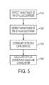
- FIG. 5illustrates an exemplary method for detecting an orientation of a stylus according to various embodiments. This method can be used with the stylus of FIGS. 2 a and 2 b , for example.
- a first capacitance formed between a stylus first electrode and a contacting surfacecan be detected ( 510 ).
- a second capacitance formed between a stylus second electrode and the contacting surfacecan be detected ( 520 ).
- the first electrodecan be a tip electrode and the second electrode can be a ring electrode.
- the capacitance detectioncan include capturing an image that can show touch or hover images resulting from the capacitances at the touch panel and performing a suitable image processing method on the captured image to determine the locations of the capacitance images therein.
- the detected capacitance images in the captured imagecan be correlated ( 530 ).
- the correlationcan include determining the proximity of the two capacitance images in order to determine the tilt of the stylus and determining the relative positions of the two capacitance images in order to determine the direction of the stylus tilt.
- the stylus orientationcan then be calculated based on the correlation ( 540 ).
- the orientation calculationcan include determining the tilt angle based on the amount of proximity between the two capacitance images in the captured image and determining the direction of the stylus tilt based on the relative positions of the two capacitance images in the captured image.
- lookup tablescan be used, where one table's entries include a tilt angle-proximity amount pairing and another table's entries includes a tilt direction-relative position pairing. The proximity amount and relative positions could be inputted to the lookup tables and the corresponding tilt angle and tilt direction outputted therefrom.
- equationscan be used, where one equation calculates tilt angle as a function of proximity amount and another equation calculates tilt direction as a function of relative position. Other orientation calculation methods are also possible according to various embodiments.
- FIG. 6 aillustrates a side view of another exemplary stylus according to various embodiments.
- stylus 610can include shaft 618 and tip 612 .
- the tip 612can include electrode 614 at the distal end of the tip for contacting a surface and segment electrodes 616 -A, 616 -B, 616 -C proximate to the distal end and forming a broken ring around the tip.
- the stylus 610 of FIG. 6 ais like the stylus 210 of FIG. 2 a , except that the ring electrode 216 of FIG. 2 a is replaced with segment electrodes 616 -A, 616 -B, 616 -C of FIG. 6 a.
- FIG. 6 billustrates a bottom view of the exemplary stylus of FIG. 6 a according to various embodiments.
- stylus 610can have a conical shaped tip 612 with electrode 614 at the distal end of the tip and segment electrodes 616 -A, 616 -B, 616 -C proximate to the distal end and forming a broken ring around the tip.
- FIG. 6 bdepicts three segment electrodes, it is to be understood that other numbers of electrodes, e.g., two, four, five, and so on, can be used according to various embodiments.
- stylus rotationcan be determined for the stylus of FIGS. 6 a and 6 b , as will be described below.
- FIGS. 7 a , 7 b , and 7 cillustrate various orientations of the exemplary stylus of FIGS. 6 a and 6 b as it touches a touch panel according to various embodiments.
- stylus 710can have a perpendicular orientation as it touches touch panel 720 .
- tip electrode 714can form capacitance C 1 with a proximate conductive element, e.g., row(s) and/or column(s), (not shown) of the panel.
- segment electrodes 716 -A, 716 -B, 716 -Ccan form capacitances C 2 , C 3 , C 4 , respectively with a proximate conductive element, e.g., row(s) and/or column(s), of the panel 720 .
- Image 730 captured at the panel 720can show touch or hover images resulting from the four capacitances C 1 , C 2 , C 3 , C 4 . Because the stylus 710 is perpendicular to the panel 720 , the image 730 can show the image resulting from the tip capacitance C 1 surrounded by the images resulting from the segment capacitances C 2 , C 3 , C 4 .
- the stylus 710can have a tilted orientation as it touches the panel 720 .
- the image 730 captured at the panel 720can show a shift in the positions of the tip capacitances C 1 image and the segment capacitance image (in this case, segment capacitance C 2 image) of the electrode (in this case, electrode 716 -A) closest to the panel 720 .
- the other segment capacitance imagescan disappear from the image 730 , as illustrated here.
- the other segment capacitance imagescan have smaller images that also shift depending on how the stylus is tilted and rotated.
- the captured image 730can also be used to determine the direction of the stylus tilt relative to the touch panel 720 .
- the segment capacitance C 2 imageis to the right of the tip capacitance C 1 image. This can indicate that the stylus 710 is tilted to the right. If the segment capacitance C 2 image is at the left of the tip capacitance C 1 image, this can indicate that the stylus 710 is tilted to the left.
- Other tilt directionse.g., upward, downward, upper left, lower right, etc., can also be determined according to the relative positions of the capacitance C 1 , C 2 images (and any of the other segment capacitance images, if they are also shown in the captured image).
- the stylus 710can have a rotated-tilted orientation as it touches the panel 720 .
- the image 730 captured at the panel 720can show another segment capacitance image (in this case, segment capacitance C 4 image) of another electrode (in this case, electrode 716 -C) closest to the panel 720 .
- the image 730can be used to determine the amount of stylus tilt and tilt direction in the same manner as in FIG. 7 b.
- the strengths of the capacitances C 2 , C 3 , C 4 at the segment electrodes 716 -A, 716 -B, 716 -C, respectively,can be used.
- the segment electrode closest to the panelcan be determined.
- the relative strength of the capacitances C 2 , C 3 , C 4can be estimated based on the magnitudes of their corresponding images in the captured image. For example, in FIG.
- the segment electrode 716 -Awould form the strongest of the capacitances and the other segment electrodes 716 -B, 716 -C would form weaker capacitances.
- the segment electrode 716 -Cwould form the strongest of the capacitances and the other electrodes 716 -A, 716 -B would form weaker capacitances. Accordingly, by measuring the decrease in the magnitude of the capacitance C 2 image of electrode 716 -A and the increase in the magnitude of the capacitance C 4 image of electrode 716 -C over the time period indicated by FIGS. 7 b and 7 c , a determination can be made regarding how much the stylus 710 rotated between the orientations illustrated in FIGS. 7 b and 7 c.
- the stylus rotationcan be determined. For example, as the stylus rotates clockwise, the capacitance C 2 , C 4 images correspondingly rotate clockwise as their magnitudes change. Accordingly, a determination can be made regarding how much the stylus 710 rotated between the orientations illustrated in FIGS. 7 b and 7 c.
- the stylus orientationcan be detected.
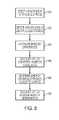
- FIG. 8illustrates another exemplary method for detecting an orientation of a stylus according to various embodiments. This method can be used with the stylus of FIGS. 6 a and 6 b , for example.
- a first capacitance formed between a stylus first electrode and a contacting surfacecan be detected ( 810 ).
- one or more second capacitances formed between one or more stylus second electrodes and the contacting surfacecan be detected ( 820 ).
- the first electrodecan be a tip electrode and the second electrode(s) can be segment electrode(s).
- the capacitance detectioncan include capturing an image that can show touch or hover images resulting from the capacitances at the touch panel and performing a suitable image processing method on the captured image to determine the locations of the capacitance images in the captured image.
- the detected capacitance images in the captured imagecan be correlated ( 830 ).
- the correlationcan include determining the proximity of the capacitance images in the captured image in order to determine the tilt of the stylus and determining the relative positions of the capacitance images in the captured image in order to determine the direction of the stylus tilt.
- the stylus tilt angle and tilt directioncan then be calculated based on the correlation ( 840 ).
- the calculationcan include determining the tilt angle based on the amount of proximity between the capacitance images in the captured image and determining the direction of the stylus tilt based on the relative positions of the capacitance images in the captured image.
- lookup tablescan be used, where one table's entries include a tilt angle-proximity amount pairing and another table's entries includes a tilt direction-relative position pairing. The proximity amount and relative positions could be inputted to the lookup tables and the corresponding tilt angle and tilt direction outputted therefrom.
- equationscan be used, where one equation calculates tilt angle as a function of proximity amount and other equation calculates tilt direction as a function of relative position. Other orientation calculation methods are also possible according to various embodiments.
- the relative strengths of the capacitance images of the second electrodes in the captured imagecan be estimated and the electrode with the strongest capacitance image magnitude determined to be the one closest to the contacting surface.
- the stylus rotationcan then be calculated based on the determination ( 860 ).
- the rotation calculationcan include detecting the capacitances of each second electrode over a particular time period, comparing each second electrode's capacitance images over the time period, and determining each second electrode's capacitance image magnitude change over that time period.
- a capacitance image increase of a particular second electrodecan indicate a rotation of that electrode toward the contacting surface.
- a capacitance image decrease of a particular second electrodecan indicate a rotation of that electrode away from the contacting surface.
- the amount and direction of the image changes and the second electrodes involvedcan indicate the amount and direction of the rotation.
- the stylusmade a small rotation clockwise. Similar determinations can be made for a large capacitance increase and concurrent capacitance decrease in these respective electrodes. Conversely, if one of the second electrodes experiences a small capacitance decrease and an adjacent (in a clockwise direction) second electrode experiences a small capacitance increase, e.g., as shown by a respective decrease and increase of image magnitudes, it can be determined that the stylus made a small rotation counterclockwise.
- a lookup tablecan be used, where the table's entries include a capacitance change amount-rotation amount pairing.
- the capacitance change amount for the appropriate second electrodescan be inputted to the lookup table and the corresponding rotation amount outputted therefrom.
- image position changescan be used to determine the stylus rotation.
- the rotation calculationcan include detecting the capacitances of each second electrode over a particular time period, comparing each second electrode's capacitance images over the time period, and determining each second electrode's capacitance image position change over that time period.
- a capacitance image clockwise shift of a particular second electrodecan indicate a clockwise rotation of the stylus.
- a capacitance image counterclockwise shift of a particular second electrodecan indicate a counterclockwise rotation of stylus.
- the amount and direction of the image shift and the second electrodes involvedcan indicate the amount and direction of the stylus rotation.
- a lookup tablecan be used, where the table's entries include a capacitance image shift amount-rotation amount pairing. The capacitance image shift amount for the appropriate second electrodes can be inputted to the lookup table and the corresponding rotation amount outputted therefrom.
- FIG. 9illustrates an exemplary stylus having an orientation sensor for use with a touch panel also having an orientation sensor according to various embodiments.
- stylus 910can include orientation sensor 919 for detecting the stylus orientation relative to a reference, e.g., the earth.
- the sensor 919can be an accelerometer, a gyroscope, a magnetometer, and the like.
- Touch panel 920can orientation sensor 929 for detecting the panel orientation relative to the reference.
- the sensor 929can be an accelerometer, a gyroscope, a magnetometer, and the like.
- the orientation of the stylus 910can be determined relative to the orientation of the panel 920 , which can be mobile.
- FIG. 10illustrates another exemplary method for detecting an orientation of a stylus according to various embodiments. This method can be used with the stylus of FIG. 9 , for example.
- a sensor in a styluscan detect the stylus orientation relative to a reference, e.g., the earth ( 1010 ).
- a sensor in a mobile touch panelcan detect the panel orientation also relative to the reference ( 1020 ). The orientation of the stylus relative to the panel can then be calculated based on the two sensed orientations ( 1030 ).
- the calculationcan include the stylus transmitting its sensor reading via wired or wireless communication to a processor, the panel transmitting its sensor reading also to the processor, and the processor calculating the orientation of the stylus based on the two transmitted orientations.
- the processorcan be in the panel, in a touch sensitive device incorporating the panel, or in a host device.
- the calculationcan be done on the stylus processor with the panel transmitting its sensor reading to the stylus. The stylus can then transmit its calculated orientation back to the panel processor, the touch sensitive device processor, or the host device processor.
- the styluscan include a second sensor to detect its orientation relative to the reference.
- the second sensorcan be a gyroscope, a magnetometer, or the like. The sensor readings from the two sensors in the stylus can then be compared to verify the orientation of the stylus. The use of the second sensor can be particularly helpful to prevent false or noisy stylus orientation readings caused by small inadvertent movement of the stylus.
- FIG. 11illustrates an exemplary stylus tip having strip electrodes according to various embodiments.
- tip 1112can have electrode 1114 at a distal end for contacting a surface and strip electrodes 1116 -A, 1116 -B, 1116 -C proximate to the distal end and aligned in parallel around the tip.
- the strip electrodescan perform in a similar manner as the segment electrodes of FIGS. 6 a and 6 b .
- FIG. 11depicts three strip electrodes, it is to be understood that any other number of multiple electrodes can be used according to various embodiments.
- FIG. 12illustrates an exemplary stylus tip having a wide ring electrode according to various embodiments.
- This stylus tipis similar to that of FIGS. 2 a and 2 b with the exception that ring electrode 1216 in FIG. 12 is wider.
- the wider ring electrodecan perform in a similar manner as the ring electrode of FIGS. 2 a and 2 b.
- FIG. 13illustrates an exemplary stylus flat tip according to various embodiments.
- two electrodes 1314 , 1316can be placed side by side to form stylus tip 1312 .
- a distal end of each electrode 1314 , 1316can be flattened to form the stylus flat tip.
- an image of the capacitances at the electrodes 1314 , 1316can be captured.
- the imagecan produce a substantially symmetric capacitance image.
- the imagecan produce an asymmetric capacitance image.
- the amount of asymmetrycan indicate the amount of tilt.
- the direction of the tiltcan be determined from the direction of the asymmetry in the capacitance image. By determining the asymmetry and its direction, the stylus tilt angle and tilt direction can be determined.
- the stylus rotationcan be determined. This determination can include detecting the capacitances of the two electrodes 1314 , 1316 over a particular time period, comparing each electrode's capacitances over the time period, and determining each electrode's capacitance change over that time period.
- a capacitance increase of a particular electrodecan indicate a rotation of that electrode toward the contacting surface.
- a capacitance decrease of a particular electrodecan indicate a rotation of that electrode away from the contacting surface.
- the styluscan act as a driving element, a sensing element, or both.
- FIG. 14 aillustrates a side view of an exemplary stylus according to various embodiments.
- stylus 1410can include shaft 1418 and tip 1412 .
- the tip 1412can include electrode 1414 forming the entire tip for contacting a surface.
- the stylus 1410 of FIG. 14 ais like the stylus 210 of FIG. 2 a , except that the tip electrode 214 and the ring electrode 216 of FIG. 2 a are replaced with the single large electrode 1414 of FIG. 14 a.
- FIG. 14 billustrates a bottom view of the exemplary stylus of FIG. 14 a according to various embodiments.
- stylus 1410can have a conical shaped tip 1412 with electrode 1414 forming the entire tip.
- FIGS. 15 a and 15 billustrate various orientations of the exemplary stylus of FIGS. 14 a and 14 b as it touches a touch panel according to various embodiments.
- stylus 1510can have a perpendicular orientation as it touches touch panel 1520 .
- electrode 1514can form capacitance C 1 with a proximate conductive element, e.g., row(s) and/or column(s), (not shown) of the panel.
- Image 1530 captured at the panel 1520can show touch or hover images resulting from the capacitance C 1 . Because the stylus 1510 is perpendicular to the panel 1520 , the image 1530 can show the capacitance C 1 image as a small circle.
- the stylus 1510can have a tilted orientation as it touches the panel 1520 .
- the image 1530 captured at the panel 1520can show a triangular shape and larger size in the touch or hover image resulting from capacitance C 1 .
- the shape and size of the capacitance C 1 imagecan be a function of the amount of stylus tilt. For example, the greater the tilt, the larger and more triangular the capacitance C 1 image shape. Conversely, the lesser the tilt, the smaller and more circular the capacitance C 1 image shape. Therefore, by determining the shape and size of the capacitance C 1 image in the captured image, the amount of stylus tilt (e.g., the tilt angle) can be determined.
- the amount of stylus tilte.g., the tilt angle
- the image 1530can also be used to determine the direction of the stylus tilt, e.g., upward, downward, right, left, and so on, relative to the touch panel 1520 .
- the capacitance C 1 imagehas a triangular shape with the triangle base to the right of the triangle apex in the captured image 1530 . This can indicate that the stylus 1510 is tilted to the right.
- the capacitance C 1 imagehas a triangular shape with the base to the left of the apex in the captured image 1530 , this can indicate that the stylus 1510 is tilted to the left.
- Other tilt directionse.g., upward, downward, upper left, lower right, etc., can also be determined according to the direction of the capacitance C 1 image's triangular base.
- the stylus orientatione.g., the tilt angle and the tilt direction, can be detected.
- FIG. 16illustrates another exemplary method for detecting an orientation of a stylus according to various embodiments. This method can be used with the stylus of FIGS. 14 a and 14 b , for example.
- a capacitance formed between a stylus electrode and a contacting surfacecan be detected ( 1610 ).
- the electrodecan be a single large electrode that forms the stylus tip.
- the capacitance detectioncan include capturing an image that can show touch or hover images resulting from the capacitance at the touch panel and performing a suitable image processing method on the captured image to determine the location of the capacitance image therein.
- the size and shape of the detected capacitance image in the captured imagecan be determined ( 1620 ). In some embodiments, performing a suitable image processing method on the captured image can determine the size and shape of the capacitance image.
- the stylus orientationcan then be calculated based on the determination ( 1630 ).
- the orientation calculationcan include determining the tilt angle based on the determined size and shape of the capacitance image and determining the direction of the stylus tilt based on the location of the triangular base relative to the triangle apex of the capacitance image.
- lookup tablescan be used, where one table's entries include a tilt angle-shape-size pairing and another table's entries includes a tilt direction-base location pairing. The shape, size, and base locations could be inputted to the lookup tables and the corresponding tilt angle and tilt direction outputted therefrom.
- equationscan be used, where one equation calculates tilt angle as a function of shape and size and another equation calculates tilt direction as a function of triangular base location. Other orientation calculation methods are also possible according to various embodiments.
- FIG. 17illustrates exemplary drive circuitry of a stylus according to various embodiments.
- stylus 1710can house drive circuitry to drive the stylus to capacitively couple with proximate conductive elements of a touch panel. The conductive elements can then output capacitance readings for further processing.
- the stylus driving circuitrycan include clock 1740 to provide a drive signal, microcontroller 1750 to control the drive signal, amplifier 1764 to gain up the clock signal to electrode 1714 , and amplifier 1766 to gain up the clock signal to electrode 1716 .
- electrode 1714can be an electrode at the distal end of the stylus tip and electrode 1716 can be one or more electrodes proximate to the distal end of the stylus tip and placed around the stylus tip.
- the signals to the two electrodes 1714 , 1716can be the same. In some embodiments, the signals to the two electrodes 1714 , 1716 can be different in order to differentiate between them.
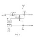
- FIG. 18illustrates exemplary sense circuitry of a stylus according to various embodiments.
- stylus 1810can house sense circuitry to sense a capacitance from proximate conductive elements of a touch panel capacitively coupled to the stylus.
- the styluscan output the capacitance readings for further processing.
- the stylus sensing circuitrycan include amplifier 1870 to receive the capacitance reading from the panel, clock 1840 to generate a demodulation signal, phase shifter 1845 to generate a phase-shifted demodulation signal, mixer 1883 to demodulate the capacitance reading with an in-phase demodulation frequency component, and mixer 1887 to demodulate the capacitance reading with a quadrature demodulation frequency component.
- the demodulated resultscan be further processed according to various embodiments.
- a styluscan house both driving and sensing circuitry and can include a switching mechanism couple between the two circuits for switching between driving and sensing according to the requirements of the system in which the stylus is used.
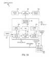
- FIG. 19illustrates an exemplary computing system that can use a stylus according to various embodiments.
- computing system 1900can include touch controller 1906 .
- the touch controller 1906can be a single application specific integrated circuit (ASIC) that can include one or more processor subsystems 1902 , which can include one or more main processors, such as ARM968 processors or other processors with similar functionality and capabilities.
- main processorssuch as ARM968 processors or other processors with similar functionality and capabilities.
- the processor functionalitycan be implemented instead by dedicated logic, such as a state machine.
- the processor subsystems 1902can also include peripherals (not shown) such as random access memory (RAM) or other types of memory or storage, watchdog timers and the like.
- RAMrandom access memory
- the touch controller 1906can also include receive section 1907 for receiving signals, such as touch (or sense) signals 1903 of one or more sense channels (not shown), other signals from other sensors such as sensor 1911 , etc.
- the touch controller 1906can also include demodulation section 1909 such as a multistage vector demodulation engine, panel scan logic 1910 , and transmit section 1914 for transmitting stimulation signals 1916 to touch panel 1924 to drive the panel.
- the scan logic 1910can access RAM 1912 , autonomously read data from the sense channels, and provide control for the sense channels.
- the scan logic 1910can control the transmit section 1914 to generate the stimulation signals 1916 at various frequencies and phases that can be selectively applied to rows of the touch panel 1924 .
- the touch controller 1906can also include charge pump 1915 , which can be used to generate the supply voltage for the transmit section 1914 .
- the stimulation signals 1916can have amplitudes higher than the maximum voltage by cascading two charge store devices, e.g., capacitors, together to form the charge pump 1915 . Therefore, the stimulus voltage can be higher (e.g., 6V) than the voltage level a single capacitor can handle (e.g., 3.6 V).
- FIG. 19shows the charge pump 1915 separate from the transmit section 1914 , the charge pump can be part of the transmit section.
- Computing system 1900can include host processor 1928 for receiving outputs from the processor subsystems 1902 and performing actions based on the outputs that can include, but are not limited to, moving an object such as a cursor or pointer, scrolling or panning, adjusting control settings, opening a file or document, viewing a menu, making a selection, executing instructions, operating a peripheral device coupled to the host device, answering a telephone call, placing a telephone call, terminating a telephone call, changing the volume or audio settings, storing information related to telephone communications such as addresses, frequently dialed numbers, received calls, missed calls, logging onto a computer or a computer network, permitting authorized individuals access to restricted areas of the computer or computer network, loading a user profile associated with a user's preferred arrangement of the computer desktop, permitting access to web content, launching a particular program, encrypting or decoding a message, and/or the like.
- host processor 1928for receiving outputs from the processor subsystems 1902 and performing actions based on the outputs that can include, but are not limited to
- the host processor 1928can also perform additional functions that may not be related to touch processing, and can be connected to program storage 1932 and display device 1930 such as an LCD for providing a UI to a user of the device.
- Display device 1930 together with touch panel 1924when located partially or entirely under the touch panel, can form a touch screen.
- Touch panel 1924can include a capacitive sensing medium having drive lines and sense lines.
- linescan sometimes be used herein to mean simply conductive pathways, as one skilled in the art can readily understand, and is not limited to structures that can be strictly linear, but can include pathways that change direction, and can include pathways of different size, shape, materials, etc.
- Drive linescan be driven by stimulation signals 1916 and resulting touch signals 1903 generated in sense lines can be transmitted to receive section 1907 in touch controller 1906 .
- drive lines and sense linescan be part of the touch and hover sensing circuitry that can interact to form capacitive sensing nodes, which can be thought of as touch picture elements (touch pixels), such as touch pixels 1926 .
- touch panel 1924can be viewed as capturing an “image” of touch.
- touch controller 1906has determined whether a touch or hover has been detected at each touch pixel in the touch panel
- the pattern of touch pixels in the touch panel at which a touch or hover occurredcan be thought of as an “image” of touch (e.g. a pattern of fingers touching or hovering over the touch panel).
- a stylus according to various embodimentscan be used to contact the touch panel 1924 .
- the stylus orientationcan provide additional information to the computing system 1900 for improved performance.
- firmwarestored in memory (e.g., one of the peripherals) and executed by the processor subsystem 1902 , or stored in the program storage 1932 and executed by the host processor 1928 .
- the firmwarecan also be stored and/or transported within any non-transitory computer readable storage medium for use by or in connection with an instruction execution system, apparatus, or device, such as a computer-based system, processor-containing system, or other system that can fetch the instructions from the instruction execution system, apparatus, or device and execute the instructions.
- a “non-transitory computer readable storage medium”can be any medium that can contain or store the program for use by or in connection with the instruction execution system, apparatus, or device.
- the non-transitory computer readable storage mediumcan include, but is not limited to, an electronic, magnetic, optical, electromagnetic, infrared, or semiconductor system, apparatus or device, a portable computer diskette (magnetic), a random access memory (RAM) (magnetic), a read-only memory (ROM) (magnetic), an erasable programmable read-only memory (EPROM) (magnetic), a portable optical disc such a CD, CD-R, CD-RW, DVD, DVD-R, or DVD-RW, or flash memory such as compact flash cards, secured digital cards, USB memory devices, memory sticks, and the like.
- the firmwarecan also be propagated within any transport medium for use by or in connection with an instruction execution system, apparatus, or device, such as a computer-based system, processor-containing system, or other system that can fetch the instructions from the instruction execution system, apparatus, or device and execute the instructions.
- a “transport medium”can be any medium that can communicate, propagate or transport the program for use by or in connection with the instruction execution system, apparatus, or device.
- the transport readable mediumcan include, but is not limited to, an electronic, magnetic, optical, electromagnetic or infrared wired or wireless propagation medium.
- touch panelas described in FIG. 19 , can sense touch and hover according to various embodiments.
- touch panel described hereincan be either single- or multi-touch.
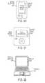
- FIG. 20illustrates an exemplary mobile telephone 2030 that can include touch panel 2024 , display device 2036 , and other computing system blocks for use with a stylus according to various embodiments.
- FIG. 21illustrates an exemplary digital media player 2130 that can include touch panel 2124 , display device 2136 , and other computing system blocks for use with a stylus according to various embodiments.
- FIG. 22illustrates an exemplary personal computer 2230 that can include touch pad 2224 , display 2236 , and other computing system blocks for use with a stylus according to various embodiments.
- the mobile telephone, media player, and personal computer of FIGS. 20 through 22can improve touch and hover sensing and preserve power by utilizing a stylus according to various embodiments.
Landscapes
- Engineering & Computer Science (AREA)
- General Engineering & Computer Science (AREA)
- Theoretical Computer Science (AREA)
- Human Computer Interaction (AREA)
- Physics & Mathematics (AREA)
- General Physics & Mathematics (AREA)
- Position Input By Displaying (AREA)
Abstract
Description
This relates generally to touch sensing and more particularly, to providing a stylus for use with a touch sensitive device and detecting an orientation of the stylus relative to the device.
Many types of input devices are available for performing operations in a computing system, such as buttons or keys, mice, trackballs, touch sensor panels, joysticks, touch pads, touch screens, and the like. Touch sensitive devices, and touch screens, in particular, are becoming increasingly popular because of their ease and versatility of operation as well as their declining price. Touch sensitive devices can include a touch sensor panel, which can be a clear panel with a touch sensitive surface, and a display device such as a liquid crystal display (LCD) that can be positioned partially or fully behind the panel, or integrated with the panel, so that the touch sensitive surface can substantially cover the viewable area of the display device. Touch sensitive devices can generally allow a user to perform various functions by touching or hovering over the touch sensor panel using one or more fingers, a stylus or other object at a location often dictated by a user interface (UI) including virtual buttons, keys, bars, displays, and other elements, being displayed by the display device. In general, touch screens can recognize a touch event and the position of the touch event on the touch sensor panel or a hover event and the position of the hover event on the touch sensor panel, and the computing system can then interpret the touch or hover event in accordance with the display appearing at the time of the event, and thereafter can perform one or more operations based on the event.
When a stylus has been used as an input device, the stylus has traditionally provided simply a touch input without additional information that can be helpful to the touch sensitive device for detecting touch or hover events.
This relates to detection of an orientation of a stylus relative to a surface. In an example, the orientation of a stylus relative to a contacting surface, e.g., a touch panel, can be detected by detecting a capacitance at one or more locations on the stylus relative to the surface, and then using the capacitance(s) to determine the orientation of the stylus relative to the surface. In another example, the orientation of a stylus relative to a contacting surface, e.g., a touch panel, can be detected by first detecting the orientation of the stylus relative to a reference, detecting the orientation of the contacting surface relative to the reference, and then calculating the orientation of the stylus relative to the contacting surface using the two detected orientations. Stylus orientation can advantageously be used to affect width and darkness of a resultant line displayed on the touch panel, thereby improving the realism of the stylus experience. The stylus can advantageously be used to improve touch and hover sensing and to preserve power savings in the contacting device.
In the following description of example embodiments, reference is made to the accompanying drawings in which it is shown by way of illustration specific embodiments that can be practiced. It is to be understood that other embodiments can be used and structural changes can be made without departing from the scope of the various embodiments.
This relates to detection of an orientation of a stylus relative to a surface. In some embodiments, the orientation of a stylus relative to a contacting surface, e.g., a touch panel, can be detected by detecting a capacitance at one or more locations on the stylus relative to the surface, and then using the capacitance(s) to determine the orientation of the stylus relative to the surface. In some embodiments, the orientation of a stylus relative to a contacting surface, e.g., a touch panel, can be detected by first detecting the orientation of the stylus relative to a reference, detecting the orientation of the contacting surface relative to the reference, and then calculating the orientation of the stylus relative to the contacting surface using the two detected orientations. Stylus orientation can advantageously be used to affect width and darkness of a resultant line displayed on the touch panel, thereby improving the realism of the stylus experience. The stylus can advantageously be used to improve touch and hover sensing and to preserve power savings in the contacting device.
Although some embodiments are described herein in terms of a stylus, it is to be understood that other input devices and/or pointing devices can be used according to various embodiments.
Although some embodiments are described herein in terms of a touch panel, it is to be understood that other touch sensitive devices capable of sensing an object touching or hovering over the devices can be used according to various embodiments.
When stylus110 touches or hovers over a surface of thetouch panel 120, the stylus can form a capacitance with one or more of theconductive rows 101 and/orcolumns 102 that can be detected by sensing circuitry (not shown). The stylus touch or hover can be represented in an image captured at thetouch panel 120 and processed for input information regarding the stylus110.
In some embodiments, the stylus110 can act as a driving element stimulated by a stimulation signal to capacitively couple with a proximateconductive row 101 orcolumn 102 of thetouch panel 120, thereby forming a capacitive path for coupling charge from the stylus to that proximate row or column. Theproximate row 101 orcolumn 102 can output signals representative of the coupling charge to the sensing circuitry.
In some embodiments, the stylus110 can act as a sensing element capacitively coupled with a proximateconductive row 101 orcolumn 102 of thetouch panel 120 that has been stimulated by a stimulation signal. The stylus110 can then output signals representative of the coupling charge to the sensing circuitry.
A stylus can have various orientations as it touches or hovers over a touch panel. In some embodiments, a particular action of the touch panel can be performed based on the stylus orientation. Accordingly, detecting the stylus orientation can be helpful in touch panel operation.
In the example ofFIG. 4 b, thestylus 410 can have a tilted orientation as it touches thepanel 420. As a result, theimage 430 captured at thepanel 420 can show a shift in the positions of the touch or hover images resulting from two capacitances C1, C2 relative to each other. Here, the ring capacitance C2 image has shifted to the right of the tip capacitance C1 image. The amount of the shift can be a function of the amount of stylus tilt. For example, the greater the tilt, the further the ring capacitance C2 image is from the tip capacitance C1 image. Conversely, the lesser the tilt, the closer the ring capacitance C2 image is and/or overlaps the tip capacitance C1 image. Therefore, by determining the proximity of the two capacitances C1, C2 images in the captured image, the amount of stylus tilt can be determined.
The image can also be used to determine the direction of the stylus tilt, e.g., upward, downward, right, left, and so on, relative to thetouch panel 420. For example, in theimage 430 ofFIG. 4 b, the ring capacitance C2 image is to the right of the tip capacitance C1 image. This can indicate that thestylus 410 is tilted to the right. If the ring capacitance C2 image is at the left of the tip capacitance C1 image, this can indicate that thestylus 410 is tilted to the left. If the ring capacitance C2 image is above the tip capacitance C1 image, this can indicate that thestylus 410 is tilted upward. If the ring capacitance C2 image is below the tip capacitance C1 image, this can indicate that thestylus 410 is tilted downward. Other tilt directions, e.g., upper left, lower right, etc., can also be determined according to the relative positions of the capacitance C1, C2 images.
By determining the proximity of the two capacitances C1, C2 to each other and their relative positions in an image, the stylus orientation can be detected.
The detected capacitance images in the captured image can be correlated (530). In some embodiments, the correlation can include determining the proximity of the two capacitance images in order to determine the tilt of the stylus and determining the relative positions of the two capacitance images in order to determine the direction of the stylus tilt.
The stylus orientation can then be calculated based on the correlation (540). In some embodiments, the orientation calculation can include determining the tilt angle based on the amount of proximity between the two capacitance images in the captured image and determining the direction of the stylus tilt based on the relative positions of the two capacitance images in the captured image. In some embodiments, lookup tables can be used, where one table's entries include a tilt angle-proximity amount pairing and another table's entries includes a tilt direction-relative position pairing. The proximity amount and relative positions could be inputted to the lookup tables and the corresponding tilt angle and tilt direction outputted therefrom. In some embodiments, equations can be used, where one equation calculates tilt angle as a function of proximity amount and another equation calculates tilt direction as a function of relative position. Other orientation calculation methods are also possible according to various embodiments.
In addition to determining stylus tilt angle and tilt direction, similar to the stylus ofFIGS. 2 aand2b, stylus rotation can be determined for the stylus ofFIGS. 6 aand6b, as will be described below.
In the example ofFIG. 7 b, thestylus 710 can have a tilted orientation as it touches thepanel 720. As a result, theimage 730 captured at thepanel 720 can show a shift in the positions of the tip capacitances C1 image and the segment capacitance image (in this case, segment capacitance C2 image) of the electrode (in this case, electrode716-A) closest to thepanel 720. The other segment capacitance images can disappear from theimage 730, as illustrated here. Alternatively, the other segment capacitance images can have smaller images that also shift depending on how the stylus is tilted and rotated. By determining the proximity of the two capacitances C1, C2 images in the captured image, the amount of stylus tilt can be determined.
The capturedimage 730 can also be used to determine the direction of the stylus tilt relative to thetouch panel 720. For example, in theimage 730 ofFIG. 7 b, the segment capacitance C2 image is to the right of the tip capacitance C1 image. This can indicate that thestylus 710 is tilted to the right. If the segment capacitance C2 image is at the left of the tip capacitance C1 image, this can indicate that thestylus 710 is tilted to the left. Other tilt directions, e.g., upward, downward, upper left, lower right, etc., can also be determined according to the relative positions of the capacitance C1, C2 images (and any of the other segment capacitance images, if they are also shown in the captured image).
In the example ofFIG. 7 c, thestylus 710 can have a rotated-tilted orientation as it touches thepanel 720. As a result, theimage 730 captured at thepanel 720 can show another segment capacitance image (in this case, segment capacitance C4 image) of another electrode (in this case, electrode716-C) closest to thepanel 720. Theimage 730 can be used to determine the amount of stylus tilt and tilt direction in the same manner as inFIG. 7 b.
To determine the amount of stylus rotation, the strengths of the capacitances C2, C3, C4 at the segment electrodes716-A,716-B,716-C, respectively, can be used. The closer an electrode is to thepanel 720, the stronger the capacitive coupling between the electrode and the panel, hence the stronger the capacitance. By estimating the strength of the capacitances relative to each other, the segment electrode closest to the panel can be determined. In some embodiments, the relative strength of the capacitances C2, C3, C4 can be estimated based on the magnitudes of their corresponding images in the captured image. For example, inFIG. 7 b, the segment electrode716-A would form the strongest of the capacitances and the other segment electrodes716-B,716-C would form weaker capacitances. InFIG. 7 c, the segment electrode716-C would form the strongest of the capacitances and the other electrodes716-A,716-B would form weaker capacitances. Accordingly, by measuring the decrease in the magnitude of the capacitance C2 image of electrode716-A and the increase in the magnitude of the capacitance C4 image of electrode716-C over the time period indicated byFIGS. 7 band7c, a determination can be made regarding how much thestylus 710 rotated between the orientations illustrated inFIGS. 7 band7c.
Additionally, by determining the relative positions of the magnitude changes, the stylus rotation can be determined. For example, as the stylus rotates clockwise, the capacitance C2, C4 images correspondingly rotate clockwise as their magnitudes change. Accordingly, a determination can be made regarding how much thestylus 710 rotated between the orientations illustrated inFIGS. 7 band7c.
By determining the proximity of the capacitance C1, C2, C3, C4 images to each other and their relative positions in the captured image and by determining the relative strengths of the segment capacitance C2, C3, C4 images and/or their relative position changes in the captured image, the stylus orientation can be detected.
The detected capacitance images in the captured image can be correlated (830). In some embodiments, the correlation can include determining the proximity of the capacitance images in the captured image in order to determine the tilt of the stylus and determining the relative positions of the capacitance images in the captured image in order to determine the direction of the stylus tilt.
The stylus tilt angle and tilt direction can then be calculated based on the correlation (840). In some embodiments, the calculation can include determining the tilt angle based on the amount of proximity between the capacitance images in the captured image and determining the direction of the stylus tilt based on the relative positions of the capacitance images in the captured image. In some embodiments, lookup tables can be used, where one table's entries include a tilt angle-proximity amount pairing and another table's entries includes a tilt direction-relative position pairing. The proximity amount and relative positions could be inputted to the lookup tables and the corresponding tilt angle and tilt direction outputted therefrom. In some embodiments, equations can be used, where one equation calculates tilt angle as a function of proximity amount and other equation calculates tilt direction as a function of relative position. Other orientation calculation methods are also possible according to various embodiments.
A determination can be made of which of the second electrodes is closest to the contacting surface (850). In some embodiments, the relative strengths of the capacitance images of the second electrodes in the captured image can be estimated and the electrode with the strongest capacitance image magnitude determined to be the one closest to the contacting surface.
The stylus rotation can then be calculated based on the determination (860). In some embodiments, the rotation calculation can include detecting the capacitances of each second electrode over a particular time period, comparing each second electrode's capacitance images over the time period, and determining each second electrode's capacitance image magnitude change over that time period. A capacitance image increase of a particular second electrode can indicate a rotation of that electrode toward the contacting surface. Conversely, a capacitance image decrease of a particular second electrode can indicate a rotation of that electrode away from the contacting surface. The amount and direction of the image changes and the second electrodes involved can indicate the amount and direction of the rotation. For example, if one of the second electrodes experiences a small capacitance increase and an adjacent (in a clockwise direction) second electrode experiences a small capacitance decrease, e.g., as shown by a respective increase and decrease of image magnitudes, it can be determined that the stylus made a small rotation clockwise. Similar determinations can be made for a large capacitance increase and concurrent capacitance decrease in these respective electrodes. Conversely, if one of the second electrodes experiences a small capacitance decrease and an adjacent (in a clockwise direction) second electrode experiences a small capacitance increase, e.g., as shown by a respective decrease and increase of image magnitudes, it can be determined that the stylus made a small rotation counterclockwise. Similar determinations can be made for a large capacitance decrease and concurrent capacitance increase in these respective electrodes. In some embodiments, a lookup table can be used, where the table's entries include a capacitance change amount-rotation amount pairing. The capacitance change amount for the appropriate second electrodes can be inputted to the lookup table and the corresponding rotation amount outputted therefrom.
In some embodiments, rather than using image magnitude changes as described in the previous paragraph, image position changes can be used to determine the stylus rotation. As such, the rotation calculation can include detecting the capacitances of each second electrode over a particular time period, comparing each second electrode's capacitance images over the time period, and determining each second electrode's capacitance image position change over that time period. A capacitance image clockwise shift of a particular second electrode can indicate a clockwise rotation of the stylus. Conversely, a capacitance image counterclockwise shift of a particular second electrode can indicate a counterclockwise rotation of stylus. The amount and direction of the image shift and the second electrodes involved can indicate the amount and direction of the stylus rotation. For example, if one of the second electrodes experiences a small clockwise shift, e.g., as shown by a small shift in the capacitance image in the captured images, it can be determined that the stylus made a small rotation clockwise. Similar determinations can be made for a large clockwise rotation. Conversely, if one of the second electrodes experiences a small counterclockwise shift, e.g., as shown by a small shift in the capacitance image in the captured images, it can be determined that the stylus made a small rotation counterclockwise. Similar determinations can be made for a large counterclockwise rotation. In some embodiments, a lookup table can be used, where the table's entries include a capacitance image shift amount-rotation amount pairing. The capacitance image shift amount for the appropriate second electrodes can be inputted to the lookup table and the corresponding rotation amount outputted therefrom.
In some embodiments, the stylus can include a second sensor to detect its orientation relative to the reference. In some embodiments, the second sensor can be a gyroscope, a magnetometer, or the like. The sensor readings from the two sensors in the stylus can then be compared to verify the orientation of the stylus. The use of the second sensor can be particularly helpful to prevent false or noisy stylus orientation readings caused by small inadvertent movement of the stylus.
To detect the orientation of a stylus having the flat tip ofFIG. 13 , an image of the capacitances at theelectrodes
In addition, the stylus rotation can be determined. This determination can include detecting the capacitances of the twoelectrodes
As described previously, the stylus can act as a driving element, a sensing element, or both.
In the example ofFIG. 15 b, the stylus1510 can have a tilted orientation as it touches thepanel 1520. As a result, theimage 1530 captured at thepanel 1520 can show a triangular shape and larger size in the touch or hover image resulting from capacitance C1. The shape and size of the capacitance C1 image can be a function of the amount of stylus tilt. For example, the greater the tilt, the larger and more triangular the capacitance C1 image shape. Conversely, the lesser the tilt, the smaller and more circular the capacitance C1 image shape. Therefore, by determining the shape and size of the capacitance C1 image in the captured image, the amount of stylus tilt (e.g., the tilt angle) can be determined.
Theimage 1530 can also be used to determine the direction of the stylus tilt, e.g., upward, downward, right, left, and so on, relative to thetouch panel 1520. For example, in theimage 1530 ofFIG. 15 b, the capacitance C1 image has a triangular shape with the triangle base to the right of the triangle apex in the capturedimage 1530. This can indicate that the stylus1510 is tilted to the right. If the capacitance C1 image has a triangular shape with the base to the left of the apex in the capturedimage 1530, this can indicate that the stylus1510 is tilted to the left. Other tilt directions, e.g., upward, downward, upper left, lower right, etc., can also be determined according to the direction of the capacitance C1 image's triangular base.
By determining the size and shape in an image, the stylus orientation, e.g., the tilt angle and the tilt direction, can be detected.
The size and shape of the detected capacitance image in the captured image can be determined (1620). In some embodiments, performing a suitable image processing method on the captured image can determine the size and shape of the capacitance image.
The stylus orientation can then be calculated based on the determination (1630). In some embodiments, the orientation calculation can include determining the tilt angle based on the determined size and shape of the capacitance image and determining the direction of the stylus tilt based on the location of the triangular base relative to the triangle apex of the capacitance image. In some embodiments, lookup tables can be used, where one table's entries include a tilt angle-shape-size pairing and another table's entries includes a tilt direction-base location pairing. The shape, size, and base locations could be inputted to the lookup tables and the corresponding tilt angle and tilt direction outputted therefrom. In some embodiments, equations can be used, where one equation calculates tilt angle as a function of shape and size and another equation calculates tilt direction as a function of triangular base location. Other orientation calculation methods are also possible according to various embodiments.
In some embodiments, a stylus can house both driving and sensing circuitry and can include a switching mechanism couple between the two circuits for switching between driving and sensing according to the requirements of the system in which the stylus is used.
Thetouch controller 1906 can also includecharge pump 1915, which can be used to generate the supply voltage for the transmitsection 1914. The stimulation signals1916 can have amplitudes higher than the maximum voltage by cascading two charge store devices, e.g., capacitors, together to form thecharge pump 1915. Therefore, the stimulus voltage can be higher (e.g., 6V) than the voltage level a single capacitor can handle (e.g., 3.6 V). AlthoughFIG. 19 shows thecharge pump 1915 separate from the transmitsection 1914, the charge pump can be part of the transmit section.
A stylus according to various embodiments can be used to contact thetouch panel 1924. The stylus orientation can provide additional information to thecomputing system 1900 for improved performance.
Note that one or more of the functions described above, can be performed, for example, by firmware stored in memory (e.g., one of the peripherals) and executed by theprocessor subsystem 1902, or stored in theprogram storage 1932 and executed by thehost processor 1928. The firmware can also be stored and/or transported within any non-transitory computer readable storage medium for use by or in connection with an instruction execution system, apparatus, or device, such as a computer-based system, processor-containing system, or other system that can fetch the instructions from the instruction execution system, apparatus, or device and execute the instructions. In the context of this document, a “non-transitory computer readable storage medium” can be any medium that can contain or store the program for use by or in connection with the instruction execution system, apparatus, or device. The non-transitory computer readable storage medium can include, but is not limited to, an electronic, magnetic, optical, electromagnetic, infrared, or semiconductor system, apparatus or device, a portable computer diskette (magnetic), a random access memory (RAM) (magnetic), a read-only memory (ROM) (magnetic), an erasable programmable read-only memory (EPROM) (magnetic), a portable optical disc such a CD, CD-R, CD-RW, DVD, DVD-R, or DVD-RW, or flash memory such as compact flash cards, secured digital cards, USB memory devices, memory sticks, and the like.
The firmware can also be propagated within any transport medium for use by or in connection with an instruction execution system, apparatus, or device, such as a computer-based system, processor-containing system, or other system that can fetch the instructions from the instruction execution system, apparatus, or device and execute the instructions. In the context of this document, a “transport medium” can be any medium that can communicate, propagate or transport the program for use by or in connection with the instruction execution system, apparatus, or device. The transport readable medium can include, but is not limited to, an electronic, magnetic, optical, electromagnetic or infrared wired or wireless propagation medium.
It is to be understood that the touch panel, as described inFIG. 19 , can sense touch and hover according to various embodiments. In addition, the touch panel described herein can be either single- or multi-touch.
The mobile telephone, media player, and personal computer ofFIGS. 20 through 22 can improve touch and hover sensing and preserve power by utilizing a stylus according to various embodiments.
Although embodiments have been fully described with reference to the accompanying drawings, it is to be noted that various changes and modifications will become apparent to those skilled in the art. Such changes and modifications are to be understood as being included within the scope of the various embodiments as defined by the appended claims.
Claims (25)
1. A method for detecting an orientation of an input device, comprising:
detecting a first capacitance, generated by a first electrode at a first location on the input device;
detecting a second capacitance, generated by a second electrode at a second location on the input device;
correlating the first and second capacitances; and
calculating the orientation of the input device based on the correlation.
2. The method ofclaim 1 , wherein detecting the first capacitance comprises:
capturing an image of the first capacitance on a touch sensitive surface; and
determining a location of the image of the first capacitance.
3. The method ofclaim 1 , wherein detecting the second capacitance comprises:
capturing an image of the second capacitance on a touch sensitive surface; and
determining a location of the image of the second capacitance.
4. The method ofclaim 1 , wherein correlating the first and second capacitances comprises:
determining proximity of the detected first and second capacitances relative to each other in an image; and
determining relative position of the detected first and second capacitances in the image.
5. The method ofclaim 1 , wherein calculating the orientation of the input device comprises:
determining the orientation based on at least one of a proximity or relative position of locations captured in an image of the detected first and second capacitances on a touch sensitive surface, wherein the closer the proximity the closer the orientation to being perpendicular with respect to the touch sensitive surface.
6. The method ofclaim 1 , comprising:
determining whether the input device has rotated based on the detected second capacitance.
7. The method ofclaim 6 , wherein determining whether the device has rotated comprises:
determining which portion of the input device forms the second capacitance; and
determining the rotation according to the determined portion.
8. A capacitive input device comprising:
a first electrode at a tip of the input device; and
a second electrode proximate to the first electrode, wherein the first electrode is configured to form a first capacitance and the second electrode is configured to form a second capacitance, the first and second capacitances for detecting an orientation of the input device.
9. The device ofclaim 8 , wherein the second electrode forms a ring around the input device at a distance from the tip.
10. The device ofclaim 8 , wherein the second electrode comprises multiple segments.
11. The device ofclaim 10 , wherein the segments form a broken ring around the input device at a distance from the tip.
12. The device ofclaim 10 , wherein the segments are aligned in parallel around the input device at a distance from the tip.
13. The device ofclaim 8 , wherein the second electrode is at the tip of the input device, the tip is flat, and the first and second electrodes are adjacent to each other, a flat surface of each of the first and second electrodes forming the flat tip.
14. The device ofclaim 8 , comprising:
a drive circuit to output a drive voltage through the first electrode, the drive circuit comprising a clock to generate the drive voltage, a microcontroller to control the drive voltage, and at least one amplifier to adjust the drive voltage.
15. The device ofclaim 8 , comprising:
a sense circuit to sense a voltage at the first electrode, the sense circuit comprising a sense amplifier to adjust the sensed voltage, a clock to generate a demodulation signal, a phase shifter to shift the phase of the demodulation signal, and a set of mixers to receive the sensed voltage and either the demodulation signal or the phase-shifted demodulation signal to demodulate the sensed voltage.
16. A method for detecting an orientation of a first device relative to a second device, comprising:
sensing with a first sensor in the first device an orientation of the first device relative to a reference;
sensing with a second sensor in the second device an orientation of the second device relative to the reference; and
calculating an orientation of the first device relative to the second device based on the sensed orientations of the first and second devices relative to the reference.
17. The method ofclaim 16 , comprising:
sensing with a third sensor in the first device the orientation of the first device relative to the reference; and
comparing the sensed orientations from the first and third sensors to confirm the orientation of the first device relative to the reference.
18. The method ofclaim 16 , comprising:
transmitting the sensed orientation of the first device to the second device.
19. The method ofclaim 18 , wherein calculating the orientation of the first device relative to the second device comprises:
upon receipt of the transmitted sensed orientation of the first device, the second device calculating the orientation of the first device relative to the second device.
20. A system comprising:
a first device including a first sensor to detect an orientation of the first device relative to a reference and a transmitter to transmit the detected orientation of the first device; and
a second device including a second sensor to detect an orientation of the second device relative to the reference, a receiver to receive the detected orientation from the first device, and a processor to calculate an orientation of the first device relative to the second device based on the detected orientations of the first and second devices relative to the reference.
21. A capacitive input device comprising:
an electrode at a tip of an input device, the electrode configured to form a capacitance having an image shape and size indicative of an orientation of the input device; and
a second electrode of the input device, the second electrode configured to form a second capacitance having an image shape and size indicative of the orientation of the input device, wherein the second electrode is located at different locating than the electrode at the tip of the input device.
22. The device ofclaim 21 , wherein the electrode forms the entire tip.
23. A method for detecting an orientation of an input device, comprising:
detecting a plurality of capacitances on the input device;
determining a shape and a size in an image of the detected capacitances; and
calculating the orientation of the input device based on the determination.
24. The method ofclaim 23 , wherein calculating the orientation of the input device comprises:
calculating the orientation based on whether the shape in the image is a triangle or a circle and based on the shape size, wherein the more circular the shape the closer the orientation to being perpendicular to a surface, and wherein the smaller the size the closer the orientation to being perpendicular to the surface.
25. The method ofclaim 23 , wherein calculating the orientation of the input device comprises:
calculating the orientation based a location of a base of a triangular image relative to an apex of the triangular image, wherein, if the base is to the right of the apex in the triangular image, the orientation is tilted to the right.
Priority Applications (2)
| Application Number | Priority Date | Filing Date | Title |
|---|---|---|---|
| US13/166,743US8638320B2 (en) | 2011-06-22 | 2011-06-22 | Stylus orientation detection |
| PCT/US2012/043025WO2012177573A2 (en) | 2011-06-22 | 2012-06-18 | Stylus orientation detection |
Applications Claiming Priority (1)
| Application Number | Priority Date | Filing Date | Title |
|---|---|---|---|
| US13/166,743US8638320B2 (en) | 2011-06-22 | 2011-06-22 | Stylus orientation detection |
Publications (2)
| Publication Number | Publication Date |
|---|---|
| US20120327042A1 US20120327042A1 (en) | 2012-12-27 |
| US8638320B2true US8638320B2 (en) | 2014-01-28 |
Family
ID=46420547
Family Applications (1)
| Application Number | Title | Priority Date | Filing Date |
|---|---|---|---|
| US13/166,743Active2031-10-15US8638320B2 (en) | 2011-06-22 | 2011-06-22 | Stylus orientation detection |
Country Status (2)
| Country | Link |
|---|---|
| US (1) | US8638320B2 (en) |
| WO (1) | WO2012177573A2 (en) |
Cited By (58)
| Publication number | Priority date | Publication date | Assignee | Title |
|---|---|---|---|---|
| US20130106724A1 (en)* | 2011-10-28 | 2013-05-02 | Atmel Corporation | Executing Gestures With Active Stylus |
| US20130106717A1 (en)* | 2011-10-28 | 2013-05-02 | Atmel Corporation | Multi-Electrode Active Stylus Tip |
| US20130106720A1 (en)* | 2011-10-28 | 2013-05-02 | Atmel Corporation | Active Stylus with High Voltage |
| US20130234967A1 (en)* | 2012-03-12 | 2013-09-12 | Matthew Stoddard | Pressure sensitive multi-tip stylus for capacitive touchscreens and methods of using same |
| US20130285990A1 (en)* | 2012-03-22 | 2013-10-31 | Samsung Electronics Co., Ltd. | Touch pen for direct information input |
| US20130321328A1 (en)* | 2012-06-04 | 2013-12-05 | Samsung Electronics Co. Ltd. | Method and apparatus for correcting pen input in terminal |
| US20140184558A1 (en)* | 2012-12-28 | 2014-07-03 | Sony Mobile Communications Ab | Electronic device and method of processing user actuation of a touch-sensitive input surface |
| US20140210744A1 (en)* | 2013-01-29 | 2014-07-31 | Yoomee SONG | Mobile terminal and controlling method thereof |
| US9116558B2 (en) | 2011-10-28 | 2015-08-25 | Atmel Corporation | Executing gestures with active stylus |
| US9176604B2 (en) | 2012-07-27 | 2015-11-03 | Apple Inc. | Stylus device |
| EP3037935A1 (en) | 2014-12-26 | 2016-06-29 | Wacom Co., Ltd. | Position pointer and signal processor |
| EP3059665A2 (en) | 2015-02-20 | 2016-08-24 | Wacom Co., Ltd. | Position pointer, signal processing circuit, signal supply controlling method and signal processing method |
| US9542014B1 (en) | 2014-06-12 | 2017-01-10 | Amazon Technologies, Inc. | Low power detection of stylus touch down |
| US20170068340A1 (en)* | 2015-09-08 | 2017-03-09 | Apple Inc. | Stylus for electronic devices |
| US9606680B1 (en) | 2014-06-12 | 2017-03-28 | Amazon Technologies, Inc. | Capacitive communication between stylus devices and computing devices |
| US9619052B2 (en) | 2015-06-10 | 2017-04-11 | Apple Inc. | Devices and methods for manipulating user interfaces with a stylus |
| US9632597B2 (en) | 2014-06-12 | 2017-04-25 | Amazon Technologies, Inc. | Configurable active stylus devices |
| US9632598B1 (en) | 2014-06-12 | 2017-04-25 | Amazon Technologies, Inc. | Stylus devices with configurable frequency |
| TWI598776B (en)* | 2016-11-10 | 2017-09-11 | 翰碩電子股份有限公司 | Capacitive stylus and tilt angle detecting mrthod thereof |
| US9864441B2 (en) | 2010-06-11 | 2018-01-09 | Microsoft Technology Licensing, Llc | Object orientation detection with a digitizer |
| CN107567612A (en)* | 2015-06-09 | 2018-01-09 | 惠普发展公司,有限责任合伙企业 | Digital pen relative to computing device incidence angle |
| TWI612446B (en)* | 2016-05-10 | 2018-01-21 | 義隆電子股份有限公司 | Touching system, stylus, and detecting method for the stylus |
| US9874966B2 (en) | 2015-04-28 | 2018-01-23 | Microsoft Technology Licensing, Llc | Electrostatic device having spaced electrodes |
| US9958990B2 (en) | 2011-10-28 | 2018-05-01 | Atmel Corporation | Authenticating with active stylus |
| US9965056B2 (en) | 2016-03-02 | 2018-05-08 | FiftyThree, Inc. | Active stylus and control circuit thereof |
| US9983731B2 (en) | 2014-02-21 | 2018-05-29 | Qualcomm Incorporated | System and method for reducing shadow effects in touch systems |
| US9996184B1 (en) | 2015-05-11 | 2018-06-12 | Mark Gordon Arnold | Touchscreen accessory and software for motion-disabled users |
| US20190064947A1 (en)* | 2017-08-31 | 2019-02-28 | Sharp Kabushiki Kaisha | Display control device, pointer display method, and non-temporary recording medium |
| US10310636B2 (en) | 2016-11-04 | 2019-06-04 | Microsoft Technology Licensing, Llc | Active stylus |
| JP2019091495A (en)* | 2019-02-21 | 2019-06-13 | 株式会社ワコム | Position indicator and signal processing apparatus |
| US10331235B2 (en) | 2016-11-23 | 2019-06-25 | Wacom Co., Ltd. | Stylus tilt detection based on bidirectional communication between stylus and stylus sensor controller |
| US20190384424A1 (en)* | 2016-06-09 | 2019-12-19 | Wacom Co., Ltd. | Active stylus with multiple sensors for receiving signals from a touch sensor |
| US10572063B2 (en) | 2017-01-09 | 2020-02-25 | Microsoft Technology Licensing, Llc | Position, tilt, and twist detection for stylus |
| US10579168B2 (en) | 2017-03-30 | 2020-03-03 | Microsoft Technology Licensing, Llc | Dual LED drive circuit |
| US10635195B2 (en) | 2017-02-28 | 2020-04-28 | International Business Machines Corporation | Controlling displayed content using stylus rotation |
| US11016586B2 (en)* | 2015-04-20 | 2021-05-25 | Wacom Co., Ltd. | Method using active stylus and sensor controller, sensor controller, and active stylus |
| US11051720B2 (en) | 2017-06-01 | 2021-07-06 | Apple Inc. | Fitness tracking for constrained-arm usage |
| US11054943B1 (en) | 2020-08-17 | 2021-07-06 | Microsoft Technology Licensing, Llc | Touch restriction region for touch-sensitive display |
| US11079821B2 (en)* | 2012-09-28 | 2021-08-03 | Wacom Co., Ltd. | Stylus communication with near-field coupling |
| US11103749B2 (en) | 2016-08-31 | 2021-08-31 | Apple Inc. | Systems and methods of swimming analysis |
| US11150770B2 (en)* | 2017-03-16 | 2021-10-19 | Samsung Electronics Co., Ltd. | Input device, electronic system and control method therefor |
| US11163407B2 (en) | 2017-03-16 | 2021-11-02 | Samsung Electronics Co., Ltd. | Input device including pen tip, electronic system and control method therefor |
| US11301093B2 (en)* | 2019-08-08 | 2022-04-12 | Shenzhen GOODIX Technology Co., Ltd. | Positive and negative voltage driving circuit, chip, active stylus and driving method |
| US11896368B2 (en) | 2016-08-31 | 2024-02-13 | Apple Inc. | Systems and methods for determining swimming metrics |
| US11937904B2 (en) | 2019-09-09 | 2024-03-26 | Apple Inc. | Detecting the end of cardio machine activities on a wearable device |
| US20240184400A1 (en)* | 2022-05-30 | 2024-06-06 | Wuhan China Star Optoelectronics Semiconductor Display Technology Co., Ltd. | Display device, driving method thereof, and active stylus thereof |
| US12032756B2 (en) | 2022-01-03 | 2024-07-09 | Samsung Display Co., Ltd. | Input device and electronic device comprising the same |
| US20240295935A1 (en)* | 2023-03-05 | 2024-09-05 | Novatek Microelectronics Corp. | Stylus, touch device, and touch processing circuit |
| US12109453B2 (en) | 2019-09-27 | 2024-10-08 | Apple Inc. | Detecting outdoor walking workouts on a wearable device |
| US12153764B1 (en)* | 2020-09-25 | 2024-11-26 | Apple Inc. | Stylus with receive architecture for position determination |
| US12277308B2 (en) | 2022-05-10 | 2025-04-15 | Apple Inc. | Interactions between an input device and an electronic device |
| US12293147B2 (en) | 2016-09-23 | 2025-05-06 | Apple Inc. | Device, method, and graphical user interface for annotating text |
| US12299218B2 (en) | 2023-06-11 | 2025-05-13 | Remarkable As | Active pen-stylus precise eraser |
| US12321589B2 (en) | 2017-06-02 | 2025-06-03 | Apple Inc. | Device, method, and graphical user interface for annotating content |
| US12340034B2 (en) | 2018-06-01 | 2025-06-24 | Apple Inc. | Devices, methods, and graphical user interfaces for an electronic device interacting with a stylus |
| US12411561B1 (en) | 2024-07-08 | 2025-09-09 | Remarkable As | Marker protection system |
| US12416999B1 (en) | 2024-07-08 | 2025-09-16 | Remarkable As | Replaceable conductive marker tip |
| US12443298B2 (en) | 2024-03-27 | 2025-10-14 | Apple Inc. | Stylus for electronic devices |
Families Citing this family (122)
| Publication number | Priority date | Publication date | Assignee | Title |
|---|---|---|---|---|
| WO2009006557A1 (en)* | 2007-07-03 | 2009-01-08 | Cypress Semiconductor Corporation | Method for improving scan time and sensitivity in touch sensitive user interface device |
| US9069405B2 (en)* | 2009-07-28 | 2015-06-30 | Cypress Semiconductor Corporation | Dynamic mode switching for fast touch response |
| US8723827B2 (en) | 2009-07-28 | 2014-05-13 | Cypress Semiconductor Corporation | Predictive touch surface scanning |
| US8723825B2 (en) | 2009-07-28 | 2014-05-13 | Cypress Semiconductor Corporation | Predictive touch surface scanning |
| US9310923B2 (en) | 2010-12-03 | 2016-04-12 | Apple Inc. | Input device for touch sensitive devices |
| US9244545B2 (en) | 2010-12-17 | 2016-01-26 | Microsoft Technology Licensing, Llc | Touch and stylus discrimination and rejection for contact sensitive computing devices |
| US9201520B2 (en)* | 2011-02-11 | 2015-12-01 | Microsoft Technology Licensing, Llc | Motion and context sharing for pen-based computing inputs |
| US8638320B2 (en) | 2011-06-22 | 2014-01-28 | Apple Inc. | Stylus orientation detection |
| US9329703B2 (en) | 2011-06-22 | 2016-05-03 | Apple Inc. | Intelligent stylus |
| US8928635B2 (en) | 2011-06-22 | 2015-01-06 | Apple Inc. | Active stylus |
| US9507441B2 (en) | 2011-09-08 | 2016-11-29 | Jcm Electronic Stylus Llc | Electronic stylus with low skew tip for capacitive touch screens |
| KR20130034765A (en)* | 2011-09-29 | 2013-04-08 | 삼성전자주식회사 | Method and device for inputting of mobile terminal using a pen |
| US9086745B2 (en)* | 2011-10-28 | 2015-07-21 | Atmel Corporation | Dynamic reconfiguration of electrodes in an active stylus |
| US9606641B2 (en) | 2015-03-09 | 2017-03-28 | Atmel Corporation | Adaptive transmit voltage in active stylus |
| US9250719B2 (en) | 2011-10-28 | 2016-02-02 | Atmel Corporation | Active stylus with filter |
| US11347330B2 (en) | 2011-10-28 | 2022-05-31 | Wacom Co., Ltd. | Adaptive transmit voltage in active stylus |
| US10725564B2 (en) | 2011-10-28 | 2020-07-28 | Wacom Co., Ltd. | Differential sensing in an active stylus |
| US9189121B2 (en) | 2011-10-28 | 2015-11-17 | Atmel Corporation | Active stylus with filter having a threshold |
| US9557833B2 (en)* | 2011-10-28 | 2017-01-31 | Atmel Corporation | Dynamic adjustment of received signal threshold in an active stylus |
| US9013429B1 (en) | 2012-01-14 | 2015-04-21 | Cypress Semiconductor Corporation | Multi-stage stylus detection |
| KR102010237B1 (en)* | 2012-07-03 | 2019-08-13 | 삼성전자주식회사 | Coordinate calibration method of digitizer, apparatus thereof, and electronic pen thereof |
| US9557845B2 (en) | 2012-07-27 | 2017-01-31 | Apple Inc. | Input device for and method of communication with capacitive devices through frequency variation |
| US9652090B2 (en) | 2012-07-27 | 2017-05-16 | Apple Inc. | Device for digital communication through capacitive coupling |
| JP6021174B2 (en)* | 2012-08-08 | 2016-11-09 | 株式会社ワコム | Position detecting device and position indicator thereof |
| KR101995403B1 (en)* | 2012-09-14 | 2019-07-02 | 삼성전자 주식회사 | Stylus pen, electroinic device and method for processing input using it |
| US9841862B2 (en)* | 2012-10-16 | 2017-12-12 | Atmel Corporation | Stylus position system |
| US9958966B2 (en) | 2012-10-16 | 2018-05-01 | Atmel Corporation | Active stylus communication and position system |
| US10013096B2 (en) | 2012-10-18 | 2018-07-03 | Atmel Corporation | Touch sensor with simultaneously driven drive electrodes |
| US20140168141A1 (en) | 2012-12-18 | 2014-06-19 | Logitech Europe S.A. | Method and system for discriminating stylus and touch interactions |
| US9158393B2 (en) | 2012-12-18 | 2015-10-13 | Logitech Europe S.A. | Active stylus for touch sensing applications |
| WO2014130355A2 (en)* | 2013-02-19 | 2014-08-28 | Jcm Electronic Stylus Llc | Electronic stylus with low skew tip for capacitive touch screens |
| US9188965B2 (en) | 2013-03-06 | 2015-11-17 | Arris Technology, Inc. | Control device including a protocol translator |
| US20140282269A1 (en)* | 2013-03-13 | 2014-09-18 | Amazon Technologies, Inc. | Non-occluded display for hover interactions |
| US10048775B2 (en) | 2013-03-14 | 2018-08-14 | Apple Inc. | Stylus detection and demodulation |
| CA2902119A1 (en) | 2013-03-15 | 2014-09-18 | Tactual Labs Co. | Fast multi-touch stylus and sensor |
| EP2972695B1 (en)* | 2013-03-15 | 2020-01-01 | Tactual Labs Co. | Stylus and fast multi-touch sensor |
| US20140327645A1 (en)* | 2013-05-06 | 2014-11-06 | Nokia Corporation | Touchscreen accessory attachment |
| TWI478036B (en)* | 2013-06-05 | 2015-03-21 | Elan Microelectronics Corp | Capacitive stylus |
| JP5990134B2 (en)* | 2013-06-11 | 2016-09-07 | 株式会社ジャパンディスプレイ | Display device with touch detection function and electronic device |
| FR3006757B1 (en)* | 2013-06-11 | 2016-10-14 | Fogale Nanotech | METHOD FOR CHARACTERIZING AN OBJECT OF INTEREST IN INTERACTION WITH A MEASURING INTERFACE, AND DEVICE IMPLEMENTING THE METHOD |
| TWI502459B (en)* | 2013-07-08 | 2015-10-01 | Acer Inc | Electronic device and touch operation method thereof |
| CN104298438B (en)* | 2013-07-17 | 2017-11-21 | 宏碁股份有限公司 | Electronic device and touch operation method thereof |
| US10067580B2 (en) | 2013-07-31 | 2018-09-04 | Apple Inc. | Active stylus for use with touch controller architecture |
| US9417717B2 (en)* | 2013-08-21 | 2016-08-16 | Htc Corporation | Methods for interacting with an electronic device by using a stylus comprising body having conductive portion and systems utilizing the same |
| US9785263B2 (en) | 2013-08-22 | 2017-10-10 | Microchip Technology Incorporated | Touch screen stylus with force and/or angle sensing functionality |
| US10228786B2 (en)* | 2013-08-30 | 2019-03-12 | Lg Electronics Inc. | Mobile terminal comprising stylus pen and touch panel |
| US9213423B2 (en) | 2013-09-13 | 2015-12-15 | Atmel Corporation | Method and system for determining stylus tilt in relation to a touch-sensing device |
| US9965053B2 (en)* | 2013-09-26 | 2018-05-08 | Sony Corporation | Touchpen for capacitive touch panel and method of detecting a position of a touchpen |
| CN104571732B (en)* | 2013-10-14 | 2018-09-21 | 深圳市汇顶科技股份有限公司 | Touch terminal, active stylus detection method and system |
| CN108279815B (en)* | 2013-11-08 | 2020-07-07 | 禾瑞亚科技股份有限公司 | Transmitter and its position detection and calculation method, touch processing device and system |
| US11237648B2 (en)* | 2013-11-08 | 2022-02-01 | Egalax_Empia Technology Inc. | Touch sensitive processing method and apparatus and touch sensitive system for reducing detection time period of tethered stylus |
| US20150138165A1 (en)* | 2013-11-21 | 2015-05-21 | Nigel Hinson | Replaceable Tip for Active Stylus |
| US9298285B2 (en)* | 2013-12-05 | 2016-03-29 | Wacom Co., Ltd. | Stylus tip shape |
| US9262012B2 (en) | 2014-01-03 | 2016-02-16 | Microsoft Corporation | Hover angle |
| US20150199941A1 (en)* | 2014-01-15 | 2015-07-16 | Nokia Corporation | 3d touch sensor reader |
| US10423245B2 (en) | 2014-01-31 | 2019-09-24 | Qualcomm Incorporated | Techniques for providing user input to a device |
| US9614724B2 (en) | 2014-04-21 | 2017-04-04 | Microsoft Technology Licensing, Llc | Session-based device configuration |
| WO2015167418A1 (en)* | 2014-04-28 | 2015-11-05 | Hewlett-Packard Development Company. L. P. | Perform a self-capacitive scan of a stylus |
| US10111099B2 (en) | 2014-05-12 | 2018-10-23 | Microsoft Technology Licensing, Llc | Distributing content in managed wireless distribution networks |
| US9430667B2 (en) | 2014-05-12 | 2016-08-30 | Microsoft Technology Licensing, Llc | Managed wireless distribution network |
| US9384335B2 (en) | 2014-05-12 | 2016-07-05 | Microsoft Technology Licensing, Llc | Content delivery prioritization in managed wireless distribution networks |
| US9384334B2 (en) | 2014-05-12 | 2016-07-05 | Microsoft Technology Licensing, Llc | Content discovery in managed wireless distribution networks |
| US9874914B2 (en) | 2014-05-19 | 2018-01-23 | Microsoft Technology Licensing, Llc | Power management contracts for accessory devices |
| JP6304814B2 (en)* | 2014-05-23 | 2018-04-04 | 株式会社ワコム | Position detecting device and position indicator |
| US10037202B2 (en) | 2014-06-03 | 2018-07-31 | Microsoft Technology Licensing, Llc | Techniques to isolating a portion of an online computing service |
| US9870083B2 (en) | 2014-06-12 | 2018-01-16 | Microsoft Technology Licensing, Llc | Multi-device multi-user sensor correlation for pen and computing device interaction |
| US9727161B2 (en) | 2014-06-12 | 2017-08-08 | Microsoft Technology Licensing, Llc | Sensor correlation for pen and touch-sensitive computing device interaction |
| US9367490B2 (en) | 2014-06-13 | 2016-06-14 | Microsoft Technology Licensing, Llc | Reversible connector for accessory devices |
| CN105468134A (en)* | 2014-09-05 | 2016-04-06 | 富泰华工业(深圳)有限公司 | Display control system, electronic device and display control method therefor |
| KR102252543B1 (en)* | 2014-09-12 | 2021-05-17 | 엘지이노텍 주식회사 | Touch Device, Touch Pen and Touch Panel |
| KR20160033951A (en)* | 2014-09-19 | 2016-03-29 | 삼성전자주식회사 | Display apparatus and Method for controlling display apparatus thereof |
| US9357493B1 (en)* | 2014-11-14 | 2016-05-31 | Amazon Technologies, Inc. | Stylus power management using motion and orientation sensing |
| KR102411868B1 (en)* | 2014-11-28 | 2022-06-23 | 삼성전자주식회사 | Electronic apparatus and method for display graphic object the same |
| US10067618B2 (en) | 2014-12-04 | 2018-09-04 | Apple Inc. | Coarse scan and targeted active mode scan for touch |
| KR102273683B1 (en)* | 2015-01-30 | 2021-07-05 | 엘지디스플레이 주식회사 | Flat panel display device using stalus pen |
| US9678584B2 (en)* | 2015-04-06 | 2017-06-13 | Microsoft Technology Licensing, Llc | Device including electrode having thickness to facilitate tracking |
| KR102356636B1 (en)* | 2015-06-26 | 2022-01-28 | 삼성전자주식회사 | Input device, electronic apparatus for receiving signal from the input device and controlling method thereof |
| EP3314380A4 (en)* | 2015-06-26 | 2018-08-22 | Samsung Electronics Co., Ltd. | Input device, electronic device for receiving signal from input device, and control method thereof |
| US9830003B2 (en) | 2015-08-18 | 2017-11-28 | Microsoft Technology Licensing, Llc | Ring button components in electronics |
| US10025401B2 (en)* | 2015-09-08 | 2018-07-17 | Apple Inc. | Active stylus ring electrode |
| US20170115753A1 (en)* | 2015-10-21 | 2017-04-27 | Waltop International Corporation | Method for detecting orientation of stylus |
| CN105511648B (en)* | 2016-01-04 | 2018-10-12 | 京东方科技集团股份有限公司 | A kind of active pen, touch input system and its driving method for touch module |
| US10254857B2 (en)* | 2016-03-06 | 2019-04-09 | Microsoft Technology Licensing, Llc | Soft touch detection of a stylus |
| US10579169B2 (en) | 2016-03-08 | 2020-03-03 | Egalax_Empia Technology Inc. | Stylus and touch control apparatus for detecting tilt angle of stylus and control method thereof |
| CN107422877B (en)* | 2016-03-08 | 2020-07-17 | 禾瑞亚科技股份有限公司 | Touch control pen providing inclination angle and pen body axial direction and control method thereof |
| CN107357472A (en)* | 2016-05-10 | 2017-11-17 | 义隆电子股份有限公司 | Touch system, touch pen and detection method thereof |
| US10637933B2 (en) | 2016-05-26 | 2020-04-28 | Logitech Europe S.A. | Method and apparatus for transferring information between electronic devices |
| US10474277B2 (en) | 2016-05-31 | 2019-11-12 | Apple Inc. | Position-based stylus communication |
| US10254862B2 (en)* | 2016-07-19 | 2019-04-09 | Asustek Computer Inc. | Stylus and touch control method |
| KR20180015987A (en)* | 2016-08-04 | 2018-02-14 | 삼성전자주식회사 | Touch sensing device for determining infomration associated with pen and method for controlling thereof and pen |
| TWI636383B (en)* | 2016-10-17 | 2018-09-21 | 禾瑞亞科技股份有限公司 | Stylus and its tip structure |
| US10261604B2 (en)* | 2016-11-04 | 2019-04-16 | Microsoft Technology Licensing, Llc | Active stylus velocity correction |
| JP6962690B2 (en)* | 2017-02-06 | 2021-11-05 | エルジー ディスプレイ カンパニー リミテッド | Tilt derivation device and tilt derivation method |
| JP6952472B2 (en)* | 2017-02-06 | 2021-10-20 | エルジー ディスプレイ カンパニー リミテッド | Tilt derivation device and tilt derivation method |
| TWI653555B (en) | 2017-04-26 | 2019-03-11 | 禾瑞亞科技股份有限公司 | Stylus and electronic system thereof |
| JP6902397B2 (en)* | 2017-05-29 | 2021-07-14 | エルジー ディスプレイ カンパニー リミテッド | Tilt derivation device and tilt derivation method |
| JP6962710B2 (en)* | 2017-05-29 | 2021-11-05 | エルジー ディスプレイ カンパニー リミテッド | Tilt derivation device and tilt derivation method |
| JP6846285B2 (en)* | 2017-05-29 | 2021-03-24 | エルジー ディスプレイ カンパニー リミテッド | Position detection device and position detection method |
| TWI630513B (en)* | 2017-08-04 | 2018-07-21 | Waltop International Corporation | Capacitive stylus providing signals for tilt and orientation detection |
| US10534464B2 (en)* | 2017-10-03 | 2020-01-14 | Microsoft Technology Licensing, Llc | Selective scanning for touch-sensitive display device |
| EP3719620B1 (en)* | 2017-11-29 | 2022-09-07 | Wacom Co., Ltd. | Communication method executed between active pen and sensor controller |
| WO2020023640A1 (en) | 2018-07-24 | 2020-01-30 | Shapirten Laboratories Llc | Power efficient stylus for an electronic device |
| TWM570464U (en)* | 2018-08-22 | 2018-11-21 | 宏碁股份有限公司 | Capacitive stylus |
| JP7225638B2 (en)* | 2018-09-26 | 2023-02-21 | 富士フイルムビジネスイノベーション株式会社 | Information processing system and program |
| CN109753164B (en)* | 2019-01-14 | 2022-06-10 | 合肥京东方光电科技有限公司 | Active pen, active pen touch system and method |
| US10884522B1 (en)* | 2019-06-19 | 2021-01-05 | Microsoft Technology Licensing, Llc | Adaptive hover operation of touch instruments |
| EP3789855A1 (en)* | 2019-09-05 | 2021-03-10 | Microsoft Technology Licensing, LLC | Stylus nib design and accuracy improvement |
| WO2021075257A1 (en)* | 2019-10-16 | 2021-04-22 | 株式会社ワコム | Electronic pen and body part for electronic pen |
| US11449175B2 (en) | 2020-03-31 | 2022-09-20 | Apple Inc. | System and method for multi-frequency projection scan for input device detection |
| CN115552361A (en) | 2020-03-31 | 2022-12-30 | 夏皮滕实验室有限责任公司 | Electrostatic discharge protection for high-efficiency stylus for electronic devices |
| US12148282B2 (en) | 2020-08-24 | 2024-11-19 | Logitech Europe S.A. | Electronic system and method for improving human interaction and activities |
| US11562638B2 (en) | 2020-08-24 | 2023-01-24 | Logitech Europe S.A. | Electronic system and method for improving human interaction and activities |
| EP4204933A1 (en) | 2020-08-27 | 2023-07-05 | Shapirten Laboratories Llc | Mechanically sensitive power efficient stylus for an electronic device |
| US11997777B2 (en) | 2020-09-24 | 2024-05-28 | Apple Inc. | Electrostatic discharge robust design for input device |
| US11460933B2 (en) | 2020-09-24 | 2022-10-04 | Apple Inc. | Shield electrode for input device |
| US11287926B1 (en) | 2020-09-25 | 2022-03-29 | Apple Inc. | System and machine learning method for detecting input device distance from touch sensitive surfaces |
| US11526240B1 (en) | 2020-09-25 | 2022-12-13 | Apple Inc. | Reducing sensitivity to leakage variation for passive stylus |
| CN112214118B (en)* | 2020-10-15 | 2024-01-26 | 维沃移动通信有限公司 | Stylus pen and control method thereof, electronic equipment |
| CN113220144B (en)* | 2021-03-15 | 2022-06-07 | 荣耀终端有限公司 | Stylus |
| US12182737B2 (en) | 2021-08-10 | 2024-12-31 | Logitech Europe S.A. | Electronic system and method for claiming and reserving work areas |
| US12242695B1 (en) | 2022-09-06 | 2025-03-04 | Apple Inc. | System and method for stylus detection |
| JP2025117718A (en)* | 2024-01-31 | 2025-08-13 | 株式会社ワコム | Cartridge and electronic pen |
Citations (393)
| Publication number | Priority date | Publication date | Assignee | Title |
|---|---|---|---|---|
| US3970846A (en) | 1973-10-29 | 1976-07-20 | Xenex Corporation | Presence detecting system with self-checking |
| US4220815A (en) | 1978-12-04 | 1980-09-02 | Elographics, Inc. | Nonplanar transparent electrographic sensor |
| US4281407A (en)* | 1979-12-14 | 1981-07-28 | Rca Corporation | Surface acoustic wave pickup and recording device |
| US4289927A (en) | 1979-11-13 | 1981-09-15 | Kurta Corporation | Graphic communication apparatus |
| US4320292A (en) | 1979-08-22 | 1982-03-16 | Nippon Telegraph And Telephone Public Corporation | Coordinate input apparatus |
| US4334219A (en) | 1979-02-28 | 1982-06-08 | Agfa-Gevaert Ag | Operation setting device having stationary touch-sensitive control elements |
| US4345248A (en) | 1979-12-14 | 1982-08-17 | Citizen Watch Company Limited | Liquid crystal display device with write-in capability |
| US4405921A (en) | 1980-05-12 | 1983-09-20 | Kabushiki Kaisha Suwa Seikosha | Liquid crystal display device |
| US4439855A (en)* | 1981-08-12 | 1984-03-27 | Rca Corporation | Capacitive playback stylus |
| US4476463A (en) | 1981-08-24 | 1984-10-09 | Interaction Systems, Inc. | Display device having unpatterned touch detection |
| US4481510A (en) | 1980-12-23 | 1984-11-06 | Thomson-Csf | Electrooptical switching device |
| US4484179A (en) | 1980-04-16 | 1984-11-20 | At&T Bell Laboratories | Touch position sensitive surface |
| US4490607A (en) | 1982-07-22 | 1984-12-25 | Igt | Pinhole objective fibre optic light pen |
| US4496981A (en) | 1981-02-26 | 1985-01-29 | Matsushita Electric Industrial Co., Ltd. | Video camera with a monitor |
| US4520357A (en)* | 1982-07-23 | 1985-05-28 | General Electric Company | Electroscopic information display and entry system with writing stylus |
| US4542375A (en) | 1982-02-11 | 1985-09-17 | At&T Bell Laboratories | Deformable touch sensitive surface |
| US4577057A (en) | 1984-03-02 | 1986-03-18 | Pencept, Inc. | Digitizing tablet system having stylus tilt correction |
| US4602321A (en) | 1985-02-28 | 1986-07-22 | Vari-Lite, Inc. | Light source having automatically variable hue, saturation and beam divergence |
| US4603356A (en) | 1984-03-19 | 1986-07-29 | Energy Conversion Devices, Inc. | Imaging system with light valve and photodetector |
| US4642459A (en) | 1985-05-17 | 1987-02-10 | International Business Machines Corporation | Light pen input system having two-threshold light sensing |
| US4644338A (en) | 1982-07-12 | 1987-02-17 | Hosiden Electronics Co., Ltd. | Dot-matrix liquid crystal display |
| US4655552A (en) | 1984-03-17 | 1987-04-07 | Citizen Watch Co., Ltd. | Flat panel display device having on-screen data input function |
| US4662718A (en) | 1983-10-20 | 1987-05-05 | Citizen Watch Co., Ltd. | Expansion system for a liquid crystal display |
| US4671671A (en) | 1984-06-18 | 1987-06-09 | Casio Computer Co., Ltd. | Small electronic apparatus with optical input device |
| US4677428A (en) | 1985-06-07 | 1987-06-30 | Hei, Inc. | Cordless light pen |
| US4679909A (en) | 1984-06-20 | 1987-07-14 | Sharp Kabushiki Kaisha | Liquid crystal input/output matrix panel |
| US4684939A (en) | 1982-06-18 | 1987-08-04 | U.S. Philips Corporation | Liquid crystal display device |
| US4698460A (en) | 1986-08-26 | 1987-10-06 | Tektronix, Inc. | Touch panel system |
| US4705942A (en) | 1985-12-26 | 1987-11-10 | American Telephone And Telegraph Company, At&T Bell Laboratories | Pressure-sensitive light pen |
| US4720869A (en) | 1986-02-18 | 1988-01-19 | International Business Machines Corporation | Hand dimension verification |
| US4736203A (en) | 1985-07-17 | 1988-04-05 | Recognition Systems, Inc. | 3D hand profile identification apparatus |
| US4749879A (en) | 1987-06-18 | 1988-06-07 | Spectra-Physics, Inc. | Signal transition detection method and system |
| US4759610A (en) | 1983-08-23 | 1988-07-26 | Kabushiki Kaisha Toshiba | Active matrix display with capacitive light shield |
| US4767192A (en) | 1986-10-31 | 1988-08-30 | International Business Machines Corporation | Light activated light valve with a silicon control element |
| US4772101A (en) | 1986-11-07 | 1988-09-20 | The United States Of America As Represented By The Administrator Of The National Aeronautics And Space Administration | Remotely controllable real-time optical processor |
| US4782328A (en) | 1986-10-02 | 1988-11-01 | Product Development Services, Incorporated | Ambient-light-responsive touch screen data input method and system |
| US4782327A (en) | 1985-01-02 | 1988-11-01 | Victor B. Kley | Computer control |
| US4785564A (en) | 1982-12-20 | 1988-11-22 | Motorola Inc. | Electronic notepad |
| US4794634A (en) | 1985-12-24 | 1988-12-27 | Kabushiki Kaisha Komatsu Seisakusho | Position-sensitive photodetector and light transmissive tablet and light-emitting pen |
| EP0306596A2 (en) | 1982-02-05 | 1989-03-15 | George A. May | High resolution light pen for use with graphic displays |
| US4814760A (en) | 1984-12-28 | 1989-03-21 | Wang Laboratories, Inc. | Information display and entry device |
| US4823178A (en) | 1984-09-29 | 1989-04-18 | Kabushiki Kaisha Toshiba | Photosensor suited for image sensor |
| US4838655A (en) | 1987-01-09 | 1989-06-13 | Hitachi, Ltd. | Projector using guest-host liquid crystal cells for improved color purity |
| US4846559A (en) | 1986-01-30 | 1989-07-11 | Messerschmitt Bclkow-Blohm GmbH | Sensor element with a memory for abnormal changes of the incident light intensity |
| US4877697A (en) | 1988-05-26 | 1989-10-31 | Hoechst Aktiengesellschaft | Color filter array for liquid crystal display device |
| US4893120A (en) | 1986-11-26 | 1990-01-09 | Digital Electronics Corporation | Touch panel using modulated light |
| US4904056A (en) | 1985-07-19 | 1990-02-27 | General Electric Company | Light blocking and cell spacing for liquid crystal matrix displays |
| US4917474A (en) | 1984-09-10 | 1990-04-17 | Semiconductor Energy Laboratory Co., Ltd. | Optoelectronic panel and method of making the same |
| US4940901A (en) | 1987-11-10 | 1990-07-10 | Thomson-Csf | X-ray imaging device |
| US5003356A (en) | 1987-09-09 | 1991-03-26 | Casio Computer Co., Ltd. | Thin film transistor array |
| EP0426469A2 (en) | 1989-11-03 | 1991-05-08 | Heikki Marttila Oy | Circuitry for compensating for the effect of light on the operation of infrared-sensitive phototransistors in a contact display panel |
| EP0426362A2 (en) | 1989-11-03 | 1991-05-08 | Heikki Marttila Oy | Switching circuit for a contact display panel |
| US5037119A (en) | 1989-01-10 | 1991-08-06 | Mazda Motor Corporation | Suspension-steering control apparatus |
| US5039206A (en) | 1987-12-02 | 1991-08-13 | The General Electric Company, P.L.C. | Liquid crystal displays |
| US5051570A (en) | 1989-01-20 | 1991-09-24 | Nec Corporation | Liquid crystal light valve showing an improved display contrast |
| US5063379A (en) | 1986-11-14 | 1991-11-05 | Robert Bosch Gmbh | Liquid crystal indicator, preferably for motor vehicles |
| US5083175A (en) | 1990-09-21 | 1992-01-21 | Xerox Corporation | Method of using offset gated gap-cell thin film device as a photosensor |
| US5105186A (en) | 1990-05-25 | 1992-04-14 | Hewlett-Packard Company | Lcd touch screen |
| US5113041A (en)* | 1990-12-28 | 1992-05-12 | At&T Bell Laboratories | Information processing |
| US5117071A (en) | 1990-10-31 | 1992-05-26 | International Business Machines Corporation | Stylus sensing system |
| US5151688A (en) | 1989-04-19 | 1992-09-29 | Sharp Kabushiki Kaisha | Input/output display panel with light pen |
| US5153420A (en) | 1990-11-28 | 1992-10-06 | Xerox Corporation | Timing independent pixel-scale light sensing apparatus |
| US5172104A (en) | 1989-02-13 | 1992-12-15 | U.S. Philips Corporation | Display device |
| US5182661A (en) | 1990-06-25 | 1993-01-26 | Nec Corporation | Thin film field effect transistor array for use in active matrix liquid crystal display |
| US5204661A (en) | 1990-12-13 | 1993-04-20 | Xerox Corporation | Input/output pixel circuit and array of such circuits |
| US5237314A (en) | 1990-11-30 | 1993-08-17 | U.S. Philips Corporation | Addressing a matrix device using electro-optical switching |
| US5236850A (en) | 1990-09-25 | 1993-08-17 | Semiconductor Energy Laboratory Co., Ltd. | Method of manufacturing a semiconductor film and a semiconductor device by sputtering in a hydrogen atmosphere and crystallizing |
| US5243332A (en) | 1991-10-31 | 1993-09-07 | Massachusetts Institute Of Technology | Information entry and display |
| EP0572009A1 (en) | 1992-05-27 | 1993-12-01 | Spacelabs Medical, Inc. | Scanning system for touch screen keyboards |
| US5276538A (en) | 1990-04-05 | 1994-01-04 | Matsushita Electric Industrial Co., Ltd. | Display device with micro lens array |
| US5301048A (en) | 1990-02-07 | 1994-04-05 | U.S. Philips Corporation | Active matrix display device with Schottky contact switching elements |
| US5308964A (en) | 1991-07-29 | 1994-05-03 | Kwon Young K | Variable resolution wand |
| US5339090A (en) | 1989-06-23 | 1994-08-16 | Northern Telecom Limited | Spatial light modulators |
| US5339091A (en) | 1986-07-07 | 1994-08-16 | Semiconductor Energy Laboratory Co., Ltd. | Paperless portable book |
| US5341133A (en) | 1991-05-09 | 1994-08-23 | The Rowland Institute For Science, Inc. | Keyboard having touch sensor keys for conveying information electronically |
| US5349174A (en) | 1992-05-06 | 1994-09-20 | U.S. Philips Corporation | Image sensor with transparent capacitive regions |
| US5360426A (en) | 1990-10-12 | 1994-11-01 | Carl-Zeiss-Stiftung | Force-controlled contact applicator for laser radiation |
| US5369262A (en) | 1992-06-03 | 1994-11-29 | Symbol Technologies, Inc. | Electronic stylus type optical reader |
| US5376948A (en) | 1992-03-25 | 1994-12-27 | Visage, Inc. | Method of and apparatus for touch-input computer and related display employing touch force location external to the display |
| US5381251A (en) | 1992-04-07 | 1995-01-10 | Sharp Kabushiki Kaisha | Optical switch element and a liquid crystal light directional coupler used in the optical switch element |
| US5386543A (en) | 1992-09-07 | 1995-01-31 | U.S. Philips Corporation | Matrix display device with light sensing function and time-shared amplifier |
| US5387445A (en) | 1991-03-08 | 1995-02-07 | Zeneca Limited | Liquid crystal display device |
| US5392058A (en)* | 1991-05-15 | 1995-02-21 | Sharp Kabushiki Kaisha | Display-integrated type tablet device |
| US5414227A (en) | 1993-04-29 | 1995-05-09 | International Business Machines Corporation | Stylus tilt detection apparatus for communication with a remote digitizing display |
| US5414283A (en) | 1993-11-19 | 1995-05-09 | Ois Optical Imaging Systems, Inc. | TFT with reduced parasitic capacitance |
| US5422693A (en) | 1991-05-10 | 1995-06-06 | Nview Corporation | Method and apparatus for interacting with a computer generated projected image |
| US5430462A (en) | 1992-12-07 | 1995-07-04 | Sharp Kabushiki Kaisha | Image input device-integrated type display device |
| US5445871A (en) | 1990-10-30 | 1995-08-29 | Kansai Paint Co., Ltd. | Surface-modified plastic plate |
| US5446564A (en) | 1992-06-03 | 1995-08-29 | Casio Computer Co., Ltd. | Liquid crystal display device having photosensor at each pixel |
| EP0491436B1 (en) | 1990-12-19 | 1995-09-27 | Philips Electronics Uk Limited | Matrix display device with write-in facility |
| US5461400A (en) | 1992-01-24 | 1995-10-24 | Sharp Kabushiki Kaisha | Display device |
| EP0366913B1 (en) | 1988-11-01 | 1995-11-22 | Mitsubishi Denki Kabushiki Kaisha | Photoelectric switching device for a coordinate detection system |
| US5483263A (en) | 1993-07-05 | 1996-01-09 | U.S. Philips Corporation | Electro-optic device |
| US5483261A (en) | 1992-02-14 | 1996-01-09 | Itu Research, Inc. | Graphical input controller and method with rear screen image detection |
| US5488204A (en) | 1992-06-08 | 1996-01-30 | Synaptics, Incorporated | Paintbrush stylus for capacitive touch sensor pad |
| US5502514A (en) | 1995-06-07 | 1996-03-26 | Nview Corporation | Stylus position sensing and digital camera with a digital micromirror device |
| US5510916A (en) | 1992-01-30 | 1996-04-23 | Nec Corporation | Active matrix liquid crystal device with opposite substrate having black matrix with larger aperture than active substrate |
| US5515186A (en) | 1991-12-26 | 1996-05-07 | Osd Envizion Company | Eye protection device for welding helmets which reduces obliquely incident light |
| US5525813A (en) | 1991-04-19 | 1996-06-11 | Fuji Xerox Co., Ltd. | Image sensor having TFT gate electrode surrounding the photoelectric conversion element |
| US5532743A (en) | 1991-05-01 | 1996-07-02 | Matsushita Electric Industrial Co., Ltd. | Solid-state image pickup device |
| EP0464908B1 (en) | 1990-06-29 | 1996-09-04 | Philips Electronics Uk Limited | Touch sensor array systems and display systems |
| US5559471A (en) | 1994-12-21 | 1996-09-24 | Motorola, Inc. | Amplifier and biasing circuit therefor |
| US5568292A (en) | 1992-09-09 | 1996-10-22 | Goldstar Co., Ltd. | Position-sensitive liquid crystal display and process for producing the same |
| US5581378A (en) | 1993-02-01 | 1996-12-03 | University Of Alabama At Huntsville | Electro-optical holographic display |
| US5585817A (en) | 1992-05-20 | 1996-12-17 | Sharp Kabushiki Kaisha | Apparatus and a method for inputting/outputting an image |
| US5589961A (en) | 1992-04-07 | 1996-12-31 | Sharp Kabushiki Kaisha | Optical wave guide driven liquid crystal display employing optical switching for input |
| US5598004A (en) | 1994-07-20 | 1997-01-28 | U.S. Philips Corporation | Image detector |
| EP0509589B1 (en) | 1991-04-17 | 1997-01-29 | Philips Electronics Uk Limited | Optical touch input device |
| US5610629A (en) | 1991-12-06 | 1997-03-11 | Ncr Corporation | Pen input to liquid crystal display |
| EP0762319A2 (en) | 1995-08-24 | 1997-03-12 | Symbios Logic Inc. | Graphical input apparatus and method |
| EP0770971A2 (en) | 1995-10-24 | 1997-05-02 | AT&T Corp. | Integrated liquid crystal display and digitizer |
| US5635982A (en) | 1994-06-27 | 1997-06-03 | Zhang; Hong J. | System for automatic video segmentation and key frame extraction for video sequences having both sharp and gradual transitions |
| US5637187A (en) | 1990-09-05 | 1997-06-10 | Seiko Instruments Inc. | Light valve device making |
| US5652600A (en) | 1994-11-17 | 1997-07-29 | Planar Systems, Inc. | Time multiplexed gray scale approach |
| US5659332A (en) | 1992-05-29 | 1997-08-19 | Sharp Kabushiki Kaisha | Display unit of input integral type |
| US5677744A (en) | 1993-05-06 | 1997-10-14 | Sharp Kabushiki Kaisha | Reflection type input/output liquid crystal display |
| EP0545709B1 (en) | 1991-12-06 | 1997-11-26 | NCR International, Inc. | Liquid crystal display apparatus |
| DE19720925A1 (en) | 1996-05-29 | 1997-12-04 | Deutsche Telekom Ag | Device for entering information |
| US5709118A (en) | 1995-06-13 | 1998-01-20 | Exedy Corporation | Press apparatus for forming gear teeth |
| US5712528A (en) | 1995-10-05 | 1998-01-27 | Planar Systems, Inc. | Dual substrate full color TFEL panel with insulator bridge structure |
| US5734491A (en) | 1996-05-30 | 1998-03-31 | Eastman Kodak Company | Electro-optic modulator with threshold bias |
| US5751453A (en) | 1991-12-06 | 1998-05-12 | Ncr Corporation | Liquid crystal display with pen-input capability |
| US5767623A (en) | 1995-09-11 | 1998-06-16 | Planar Systems, Inc. | Interconnection between an active matrix electroluminescent display and an electrical cable |
| US5777713A (en) | 1995-04-26 | 1998-07-07 | International Business Machines Corporation | Liquid crystal display unit with spacers form in the light shielding regions |
| US5778108A (en) | 1996-06-07 | 1998-07-07 | Electronic Data Systems Corporation | Method and system for detecting transitional markers such as uniform fields in a video signal |
| US5790106A (en)* | 1994-11-15 | 1998-08-04 | Alps Electric Co., Ltd. | Coordinate input apparatus with pen and finger input detection |
| US5793342A (en) | 1995-10-03 | 1998-08-11 | Planar Systems, Inc. | Resonant mode active matrix TFEL display excitation driver with sinusoidal low power illumination input |
| US5796121A (en) | 1997-03-25 | 1998-08-18 | International Business Machines Corporation | Thin film transistors fabricated on plastic substrates |
| US5796473A (en) | 1995-03-20 | 1998-08-18 | Honda Giken Kogyo Kabushiki Kaisha | Method of adjusting optical axis of headlight of vehicle |
| US5812109A (en) | 1994-08-23 | 1998-09-22 | Canon Kabushiki Kaisha | Image input/output apparatus |
| US5818956A (en) | 1995-10-23 | 1998-10-06 | Tuli; Raja Singh | Extended fingerprint reading apparatus |
| US5818553A (en) | 1995-04-10 | 1998-10-06 | Norand Corporation | Contrast control for a backlit LCD |
| US5818037A (en) | 1996-04-09 | 1998-10-06 | Tv Interactive Data Corporation | Controller using a flexible element to vary light transferred to a photosensitive element |
| US5825352A (en) | 1996-01-04 | 1998-10-20 | Logitech, Inc. | Multiple fingers contact sensing method for emulating mouse buttons and mouse operations on a touch sensor pad |
| US5831693A (en) | 1996-02-22 | 1998-11-03 | Honeywell | Integrated light sensor for an active matrix liquid crystal display panel |
| US5834765A (en) | 1997-07-08 | 1998-11-10 | Ledalite Architectural Products, Inc. | Integral ambient light and occupancy sensor having a linear array of sensor element and a segmented slit aperture device |
| US5835079A (en) | 1996-06-13 | 1998-11-10 | International Business Machines Corporation | Virtual pointing device for touchscreens |
| US5838290A (en) | 1996-03-18 | 1998-11-17 | U.S. Philips Corporation | Display device with photovoltaic converter |
| US5852487A (en) | 1996-01-25 | 1998-12-22 | Sharp Kabushiki Kaisha | LCD device having an input function and polymer substrates having dual function |
| US5877735A (en) | 1995-06-23 | 1999-03-02 | Planar Systems, Inc. | Substrate carriers for electroluminescent displays |
| US5880411A (en) | 1992-06-08 | 1999-03-09 | Synaptics, Incorporated | Object position detector with edge motion feature and gesture recognition |
| US5883715A (en) | 1995-06-20 | 1999-03-16 | Robert Bosch Gmbh | Laser vibrometer for vibration measurements |
| US5890799A (en) | 1995-05-18 | 1999-04-06 | Motorola Inc. | Method for reducing power consumption in a portable electronic device with a liquid crystal display screen |
| US5905489A (en)* | 1996-02-16 | 1999-05-18 | Sharp Kabushiki Kaisha | Coordinate input device |
| US5917464A (en) | 1994-10-18 | 1999-06-29 | Xerox Corporation | Combination of 2-D detector array with display for image processing |
| US5920360A (en) | 1996-06-07 | 1999-07-06 | Electronic Data Systems Corporation | Method and system for detecting fade transitions in a video signal |
| US5923320A (en)* | 1994-08-10 | 1999-07-13 | Fujitsu Limited | Liquid-crystal display having the capability of a tablet |
| US5926238A (en) | 1992-12-11 | 1999-07-20 | Canon Kabushiki Kaisha | Image display device, semiconductor device and optical element |
| US5930591A (en) | 1997-04-23 | 1999-07-27 | Litton Systems Canada Limited | High resolution, low voltage flat-panel radiation imaging sensors |
| US5940049A (en) | 1995-10-23 | 1999-08-17 | Polycom, Inc. | Remote interactive projector with image enhancement |
| US5942761A (en) | 1995-06-07 | 1999-08-24 | Tuli; Raja Singh | Enhancement methods and devices for reading a fingerprint image |
| US5959617A (en) | 1995-08-10 | 1999-09-28 | U.S. Philips Corporation | Light pen input systems |
| US5959697A (en) | 1996-06-07 | 1999-09-28 | Electronic Data Systems Corporation | Method and system for detecting dissolve transitions in a video signal |
| EP0618527B1 (en) | 1993-03-29 | 1999-09-29 | NCR International, Inc. | Input means for liquid crystal display |
| US5962856A (en) | 1995-04-28 | 1999-10-05 | Sunnybrook Hospital | Active matrix X-ray imaging array |
| US5966108A (en) | 1994-06-06 | 1999-10-12 | Ditzik; Richard J. | Direct view display device integration techniques |
| US5973312A (en) | 1997-02-13 | 1999-10-26 | U.S. Philips Corporation | Array of photosensitive pixels |
| US5990980A (en) | 1997-12-23 | 1999-11-23 | Sarnoff Corporation | Detection of transitions in video sequences |
| US5990988A (en) | 1995-09-01 | 1999-11-23 | Pioneer Electric Corporation | Reflection liquid crystal display and a semiconductor device for the display |
| US5995172A (en) | 1997-01-02 | 1999-11-30 | Nec Corporation | Tablet integrated liquid crystal display apparatus with less parallax |
| EP0962881A2 (en) | 1998-06-04 | 1999-12-08 | Wacom Co., Ltd. | Coordinate input stylus |
| JP2000020241A (en) | 1998-06-26 | 2000-01-21 | Sumitomo Chem Co Ltd | Touch panel |
| US6020945A (en) | 1996-11-11 | 2000-02-01 | Dowa Mining Co., Ltd. | Display device with a transparent optical filter |
| US6020590A (en) | 1998-01-22 | 2000-02-01 | Ois Optical Imaging Systems, Inc. | Large area imager with UV blocking layer |
| US6023307A (en) | 1996-11-20 | 2000-02-08 | Samsung Display Devices Co., Ltd. | Liquid crystal display with photo conversion elements on a black matrix between color filter plates |
| US6028581A (en) | 1997-10-21 | 2000-02-22 | Sony Corporation | Method and apparatus for a liquid crystal display (LCD) having an input function |
| US6049428A (en) | 1994-11-18 | 2000-04-11 | Optiva, Inc. | Dichroic light polarizers |
| US6061177A (en) | 1996-12-19 | 2000-05-09 | Fujimoto; Kenneth Noboru | Integrated computer display and graphical input apparatus and method |
| US6067140A (en) | 1997-03-03 | 2000-05-23 | Lg Electronics Inc. | Liquid crystal display device and method of manufacturing same |
| US6069393A (en) | 1987-06-26 | 2000-05-30 | Canon Kabushiki Kaisha | Photoelectric converter |
| JP2000163031A (en) | 1998-11-25 | 2000-06-16 | Seiko Epson Corp | Portable information devices and information storage media |
| US6078378A (en) | 1997-11-24 | 2000-06-20 | Industrial Technology Research Institute | Liquid crystal display with pixels having an opening formed from a photosensitive resin with spacers attached |
| US6087599A (en) | 1997-11-24 | 2000-07-11 | The Whitaker Corporation | Touch panels having plastic substrates |
| EP1022675A2 (en) | 1999-01-20 | 2000-07-26 | Sharp Kabushiki Kaisha | Image reading apparatus |
| US6100538A (en) | 1997-06-13 | 2000-08-08 | Kabushikikaisha Wacom | Optical digitizer and display means for providing display of indicated position |
| US6118435A (en) | 1997-04-10 | 2000-09-12 | Idec Izumi Corporation | Display unit with touch panel |
| US6133906A (en) | 1993-03-15 | 2000-10-17 | Microtouch Systems, Inc. | Display-integrated stylus detection system |
| US6163313A (en) | 1997-12-12 | 2000-12-19 | Aroyan; James L. | Touch sensitive screen and method |
| US6177302B1 (en) | 1990-11-09 | 2001-01-23 | Semiconductor Energy Laboratory Co., Ltd. | Method of manufacturing a thin film transistor using multiple sputtering chambers |
| US6181394B1 (en) | 1999-01-22 | 2001-01-30 | White Electronic Designs, Corp. | Super bright low reflection liquid crystal display |
| US6184873B1 (en) | 1998-01-20 | 2001-02-06 | Electronics For Imaging, Inc. | Pen positioning system |
| US6184863B1 (en) | 1998-10-13 | 2001-02-06 | The George Washington University | Direct pointing apparatus and method therefor |
| US6182892B1 (en) | 1998-03-25 | 2001-02-06 | Compaq Computer Corporation | Smart card with fingerprint image pass-through |
| US6188391B1 (en) | 1998-07-09 | 2001-02-13 | Synaptics, Inc. | Two-layer capacitive touchpad and method of making same |
| US6188781B1 (en) | 1998-07-28 | 2001-02-13 | Digital Persona, Inc. | Method and apparatus for illuminating a fingerprint through side illumination of a platen |
| US20010000676A1 (en) | 1997-10-20 | 2001-05-03 | Hongyong Zhang | Integral-type liquid crystal panel with image sensor function |
| US6232607B1 (en) | 1996-05-08 | 2001-05-15 | Ifire Technology Inc. | High resolution flat panel for radiation imaging |
| US6236063B1 (en) | 1998-05-15 | 2001-05-22 | Semiconductor Energy Laboratory Co., Ltd. | Semiconductor device |
| US6236053B1 (en) | 1998-05-05 | 2001-05-22 | E1-Mul Technologies Ltd. | Charged particle detector |
| US6242729B1 (en) | 1998-03-23 | 2001-06-05 | Sharp Kabushiki Kaisha | Two-dimensional image detector |
| US20010003711A1 (en) | 1997-06-03 | 2001-06-14 | Christopher R. Coyer | Security systems for use in gaming and methods therefor |
| US6262408B1 (en) | 1998-01-20 | 2001-07-17 | Sharp Kabushiki Kaisha | Two-dimensional image detector and process for manufacturing the same |
| US6265792B1 (en) | 1999-09-08 | 2001-07-24 | Endosonics Corporation | Medical device having precision interconnect |
| US6271813B1 (en) | 1996-08-30 | 2001-08-07 | Lear Automotive Dearborn, Inc. | Voltage control for adjusting the brightness of a screen display |
| US6278444B1 (en) | 1998-08-21 | 2001-08-21 | Geoffrey D. Wilson | Low current four-wire interface for five-wire resistive touch-screen |
| US6278423B1 (en) | 1998-11-24 | 2001-08-21 | Planar Systems, Inc | Active matrix electroluminescent grey scale display |
| EP1128170A1 (en) | 2000-02-25 | 2001-08-29 | Telefonaktiebolaget L M Ericsson (Publ) | Photodiode bias circuit |
| US6284558B1 (en) | 1997-11-25 | 2001-09-04 | Nec Corporation | Active matrix liquid-crystal display device and method for making the same |
| US6295113B1 (en) | 1998-12-16 | 2001-09-25 | Picvue Electronics, Ltd. | Twisted nematic color liquid crystal display |
| US6300977B1 (en) | 1995-04-07 | 2001-10-09 | Ifire Technology Inc. | Read-out circuit for active matrix imaging arrays |
| US6310610B1 (en) | 1997-12-04 | 2001-10-30 | Nortel Networks Limited | Intelligent touch display |
| US6316790B1 (en) | 1982-04-30 | 2001-11-13 | Seiko Epson Corporation | Active matrix assembly with light blocking layer over channel region |
| US6320617B1 (en) | 1995-11-07 | 2001-11-20 | Eastman Kodak Company | CMOS active pixel sensor using a pinned photo diode |
| US20010044858A1 (en) | 1999-12-21 | 2001-11-22 | Junichi Rekimoto | Information input/output system and information input/output method |
| US6323846B1 (en) | 1998-01-26 | 2001-11-27 | University Of Delaware | Method and apparatus for integrating manual input |
| US6323490B1 (en) | 1998-03-20 | 2001-11-27 | Kabushiki Kaisha Toshiba | X-ray semiconductor detector |
| US20010046013A1 (en) | 1998-09-16 | 2001-11-29 | Kazuto Noritake | Reflection type liquid crystal display |
| US6327376B1 (en) | 1997-12-04 | 2001-12-04 | U.S. Philips Corporation | Electronic apparatus comprising fingerprint sensing devices |
| US6326956B1 (en) | 1998-08-24 | 2001-12-04 | Intertactile Technologies Corporation | Circuit control devices utilizing electronic display screen light |
| US20010052597A1 (en) | 2000-06-20 | 2001-12-20 | U.S. Philips Corporation | Light-emitting matrix array display devices with light sensing elements |
| US20010055008A1 (en) | 2000-06-20 | 2001-12-27 | U.S. Philips Corporation | Matrix array display devices with light sensing elements and associated storage capacitors |
| US6351260B1 (en) | 1997-03-14 | 2002-02-26 | Poa Sana, Inc. | User input device for a computer system |
| US6351076B1 (en) | 1999-10-06 | 2002-02-26 | Tohoku Pioneer Corporation | Luminescent display panel drive unit and drive method thereof |
| US20020027164A1 (en) | 2000-09-07 | 2002-03-07 | Mault James R. | Portable computing apparatus particularly useful in a weight management program |
| US20020030581A1 (en) | 2000-04-14 | 2002-03-14 | Janiak Martin J. | Optical and smart card identification reader |
| US20020030768A1 (en) | 1999-03-15 | 2002-03-14 | I-Wei Wu | Integrated high resolution image sensor and display on an active matrix array with micro-lens |
| US6357939B1 (en) | 2001-02-02 | 2002-03-19 | Hewlett-Packard Company | Method of and apparatus for handheld printing of images on a media |
| US6364829B1 (en) | 1999-01-26 | 2002-04-02 | Newton Laboratories, Inc. | Autofluorescence imaging system for endoscopy |
| US6377249B1 (en) | 1997-11-12 | 2002-04-23 | Excel Tech | Electronic light pen system |
| US6380995B1 (en) | 1998-08-06 | 2002-04-30 | Lg.Philips Lcd Co., Ltd. | Transflective liquid crystal display device with asymmetry reflective electrode having a transparent portion facing a main viewing angle |
| US20020052192A1 (en) | 2000-05-09 | 2002-05-02 | Shunpei Yamazaki | User identity authentication system and user identity authenication method and mobile telephonic device |
| US6392254B1 (en) | 1997-01-17 | 2002-05-21 | General Electric Company | Corrosion resistant imager |
| US20020063518A1 (en) | 2000-08-23 | 2002-05-30 | Satoru Okamoto | Portable electronic device |
| US6399166B1 (en) | 1996-04-15 | 2002-06-04 | Optiva, Inc. | Liquid crystal display and method |
| US6400359B1 (en)* | 1998-08-27 | 2002-06-04 | Pentel Kabushiki Kaisha | Apparatus for detecting an approaching conductor, or an approach point of a conductor and an electrostatic capacity type touch panel apparatus |
| US20020067845A1 (en) | 2000-12-05 | 2002-06-06 | Griffis Andrew J. | Sensor apparatus and method for use in imaging features of an object |
| US20020071074A1 (en) | 1998-11-26 | 2002-06-13 | Kazuto Noritake | Liquid crystal display device |
| US20020074549A1 (en) | 1999-06-03 | 2002-06-20 | Woon-Yong Park | Method for fabricating thin film transistor array substrate for liquid crystal display |
| US20020080263A1 (en) | 2000-10-26 | 2002-06-27 | Krymski Alexander I. | Wide dynamic range operation for CMOS sensor with freeze-frame shutter |
| US20020080123A1 (en) | 2000-12-26 | 2002-06-27 | International Business Machines Corporation | Method for touchscreen data input |
| US20020126240A1 (en) | 2001-01-15 | 2002-09-12 | Masahiro Seiki | Liquid crystal display |
| US6453008B1 (en) | 1999-07-29 | 2002-09-17 | Kabushiki Kaisha Toshiba | Radiation detector noise reduction method and radiation detector |
| US6465824B1 (en) | 2000-03-09 | 2002-10-15 | General Electric Company | Imager structure |
| US20020149571A1 (en) | 2001-04-13 | 2002-10-17 | Roberts Jerry B. | Method and apparatus for force-based touch input |
| US6476447B1 (en) | 1992-02-05 | 2002-11-05 | Semiconductor Energy Laboratory Co., Ltd. | Active matrix display device including a transistor |
| US20020175903A1 (en) | 2001-05-11 | 2002-11-28 | Christer Fahraeus | Electronic pen |
| JP2002342033A (en) | 2001-05-21 | 2002-11-29 | Sony Corp | Non-contact type user input device |
| US6495387B2 (en) | 1999-12-10 | 2002-12-17 | Koninklijke Philips Electronics N.V. | Electronic devices including micromechanical switches |
| US6504530B1 (en) | 1999-09-07 | 2003-01-07 | Elo Touchsystems, Inc. | Touch confirming touchscreen utilizing plural touch sensors |
| US6518561B1 (en) | 1999-11-05 | 2003-02-11 | Sony Corporation | User detection circuit with environmental light detector |
| US6521109B1 (en) | 1999-09-13 | 2003-02-18 | Interuniversitair Microelektronica Centrum (Imec) Vzw | Device for detecting an analyte in a sample based on organic materials |
| US20030038778A1 (en) | 2001-08-13 | 2003-02-27 | Siemens Information And Communication Mobile, Llc | Tilt-based pointing for hand-held devices |
| US6529189B1 (en) | 2000-02-08 | 2003-03-04 | International Business Machines Corporation | Touch screen stylus with IR-coupled selection buttons |
| US6552745B1 (en) | 1998-04-08 | 2003-04-22 | Agilent Technologies, Inc. | CMOS active pixel with memory for imaging sensors |
| US20030103030A1 (en) | 2001-12-04 | 2003-06-05 | Desun System Inc. | Two-in-one image display/image capture apparatus and the method thereof and identification system using the same |
| US20030117369A1 (en) | 1992-03-13 | 2003-06-26 | Kopin Corporation | Head-mounted display system |
| US6597348B1 (en) | 1998-12-28 | 2003-07-22 | Semiconductor Energy Laboratory Co., Ltd. | Information-processing device |
| US20030137494A1 (en) | 2000-05-01 | 2003-07-24 | Tulbert David J. | Human-machine interface |
| US6603867B1 (en) | 1998-09-08 | 2003-08-05 | Fuji Xerox Co., Ltd. | Three-dimensional object identifying system |
| US20030151569A1 (en) | 2002-02-12 | 2003-08-14 | Eastman Kodak Company | Flat-panel light emitting pixel with luminance feedback |
| US20030156087A1 (en) | 2002-02-20 | 2003-08-21 | Boer Willem Den | Light sensitive display |
| US20030156100A1 (en) | 2002-02-19 | 2003-08-21 | Palm, Inc. | Display system |
| US20030174870A1 (en) | 2002-03-12 | 2003-09-18 | Kim Choong Hoo | Liquid crystal display device performing both image display mode and fingerprint recognition mode |
| US20030174256A1 (en) | 2002-03-12 | 2003-09-18 | Kim Choong Hoo | Liquid crystal display device performing both image display mode and fingerprint recognition mode |
| US20030183019A1 (en) | 2002-03-29 | 2003-10-02 | Testech Inc. | Slim type fingerprint recognition device using contact light emitting device and thin film transistor fingerprint input device |
| US20030197691A1 (en)* | 2002-04-19 | 2003-10-23 | Koji Fujiwara | Input device and I/O-integrated display |
| US20030205662A1 (en) | 2002-02-20 | 2003-11-06 | Planar Systems, Inc. | Image sensor with photosensitive thin film transistors and dark current compensation |
| US6646636B1 (en) | 1999-10-29 | 2003-11-11 | Digilens Inc. | Display system utilizing ambient light and a dedicated light source |
| US20030231277A1 (en) | 1999-03-17 | 2003-12-18 | Fujitsu Display Technologies Corporation | Method for manufacturing liquid crystal panel, liquid crystal panel and manufacturing system of the same |
| US6667740B2 (en) | 1998-11-27 | 2003-12-23 | Synaptics (Uk) Limited | Position sensor |
| US20030234759A1 (en) | 2002-06-21 | 2003-12-25 | Johan Bergquist | Display circuit with optical sensor |
| US20040008189A1 (en) | 2002-07-10 | 2004-01-15 | Clapper Edward O. | Multi-mouse actions stylus |
| US6681034B1 (en) | 1999-07-15 | 2004-01-20 | Precise Biometrics | Method and system for fingerprint template matching |
| US6679702B1 (en) | 2001-12-18 | 2004-01-20 | Paul S. Rau | Vehicle-based headway distance training system |
| US6690387B2 (en) | 2001-12-28 | 2004-02-10 | Koninklijke Philips Electronics N.V. | Touch-screen image scrolling system and method |
| US6738050B2 (en)* | 1998-05-12 | 2004-05-18 | E Ink Corporation | Microencapsulated electrophoretic electrostatically addressed media for drawing device applications |
| US20040095333A1 (en) | 2002-08-29 | 2004-05-20 | N-Trig Ltd. | Transparent digitiser |
| US6741655B1 (en) | 1997-05-05 | 2004-05-25 | The Trustees Of Columbia University In The City Of New York | Algorithms and system for object-oriented content-based video search |
| US20040113877A1 (en) | 2002-05-23 | 2004-06-17 | Adiel Abileah | Light sensitive display |
| US20040125430A1 (en) | 2002-07-04 | 2004-07-01 | Yasushi Kasajima | Display device and electronic equipment having the same |
| US6762741B2 (en) | 2000-12-22 | 2004-07-13 | Visteon Global Technologies, Inc. | Automatic brightness control system and method for a display device using a logarithmic sensor |
| US20040140962A1 (en) | 2003-01-21 | 2004-07-22 | Microsoft Corporation | Inertial sensors integration |
| US20040189587A1 (en) | 2003-03-28 | 2004-09-30 | Jung Yong Chae | Liquid crystal display device having electromagnetic type touch panel |
| US20040191976A1 (en) | 2003-03-27 | 2004-09-30 | Texas Instruments Incorporated | Adjusting the strength of output buffers |
| US6803906B1 (en) | 2000-07-05 | 2004-10-12 | Smart Technologies, Inc. | Passive touch system and method of detecting user input |
| US6815716B2 (en) | 2000-09-19 | 2004-11-09 | Thales Avionics Lcd S.A. | Tft matrix for optical sensor comprising a photosensitive semiconductor layer, and optical sensor comprising such an active matrix |
| US20040252867A1 (en) | 2000-01-05 | 2004-12-16 | Je-Hsiung Lan | Biometric sensor |
| US20050007125A1 (en) | 2003-07-11 | 2005-01-13 | Heger Charles E. | Dual axis capacitive level sensor |
| US20050040393A1 (en) | 2003-08-22 | 2005-02-24 | Hong Sungkwon C. | Imaging with gate controlled charge storage |
| US6862022B2 (en) | 2001-07-20 | 2005-03-01 | Hewlett-Packard Development Company, L.P. | Method and system for automatically selecting a vertical refresh rate for a video display monitor |
| US6864882B2 (en) | 2000-05-24 | 2005-03-08 | Next Holdings Limited | Protected touch panel display system |
| US6879344B1 (en) | 1999-11-08 | 2005-04-12 | Casio Computer Co., Ltd. | Photosensor system and drive control method thereof |
| US6879710B1 (en) | 1999-04-05 | 2005-04-12 | Sharp Kabushiki Kaisha | Authentication apparatus using a display/fingerprint reader |
| US20050091297A1 (en) | 2002-07-30 | 2005-04-28 | Canon Kabushiki Kaisha | Coordinate input apparatus and control method thereof, coordinate input pointing tool, and program |
| US6888528B2 (en) | 1998-06-29 | 2005-05-03 | Sanyo Electric Co., Ltd. | Liquid crystal display apparatus having light collecting mechanism |
| JP2005129948A (en) | 2003-10-23 | 2005-05-19 | Samsung Electronics Co Ltd | Photosensitive element, array substrate having the same, and liquid crystal display device |
| US20050110777A1 (en) | 2003-11-25 | 2005-05-26 | Geaghan Bernard O. | Light-emitting stylus and user input device using same |
| US20050134749A1 (en) | 2003-12-19 | 2005-06-23 | Adiel Abileah | Reflection resistant display |
| US20050146517A1 (en) | 2003-12-30 | 2005-07-07 | Robrecht Michael J. | Passive light stylus and user input device using same |
| US20050173703A1 (en) | 2001-06-29 | 2005-08-11 | Hugues Lebrun | Active matrix of thin-film transistors (tft) for an optical sensors or display screen |
| US20050179706A1 (en) | 2004-02-18 | 2005-08-18 | Childers Winthrop D. | Method and system for reducing gray scale discontinuities in contrast enhancing screens affected by ambient light |
| US20050200603A1 (en) | 2002-01-30 | 2005-09-15 | Microsoft Corporation | Proximity sensor with adaptive threshold |
| US6947017B1 (en) | 2001-08-29 | 2005-09-20 | Palm, Inc. | Dynamic brightness range for portable computer displays based on ambient conditions |
| US20050206764A1 (en) | 1998-02-20 | 2005-09-22 | Canon Kabushiki Kaisha | Photoelectric converter and radiation reader |
| US20050231656A1 (en) | 2004-04-16 | 2005-10-20 | Planar Systems, Inc. | Image sensor with photosensitive thin film transistors and dark current compensation |
| US6972753B1 (en) | 1998-10-02 | 2005-12-06 | Semiconductor Energy Laboratory Co., Ltd. | Touch panel, display device provided with touch panel and electronic equipment provided with display device |
| US20050270590A1 (en) | 2002-10-24 | 2005-12-08 | Yoshihiro Izumi | Image reading device and image reading method |
| US20060007224A1 (en) | 2004-05-31 | 2006-01-12 | Toshiba Matsushita Display Technology Co., Ltd. | Image capturing function-equipped display device |
| US20060007336A1 (en) | 2002-09-12 | 2006-01-12 | Takumi Yamaguchi | Solid-state image pickup device, and manufacturing method thereof |
| US20060010658A1 (en) | 2002-06-26 | 2006-01-19 | Mark Bigley | Snap fastener for use with fabrics |
| US20060026521A1 (en) | 2004-07-30 | 2006-02-02 | Apple Computer, Inc. | Gestures for touch sensitive input devices |
| US20060034492A1 (en) | 2002-10-30 | 2006-02-16 | Roy Siegel | Hand recognition system |
| US7009663B2 (en) | 2003-12-17 | 2006-03-07 | Planar Systems, Inc. | Integrated optical light sensitive active matrix liquid crystal display |
| US7015894B2 (en) | 2001-09-28 | 2006-03-21 | Ricoh Company, Ltd. | Information input and output system, method, storage medium, and carrier wave |
| US20060120013A1 (en) | 2003-08-05 | 2006-06-08 | Impinj, Inc. | High-voltage CMOS-compatible capacitors |
| US20060170658A1 (en) | 2005-02-03 | 2006-08-03 | Toshiba Matsushita Display Technology Co., Ltd. | Display device including function to input information from screen by light |
| US20060176288A1 (en) | 1998-08-18 | 2006-08-10 | Arkady Pittel | Electronic pen holding |
| US7098894B2 (en) | 2000-12-15 | 2006-08-29 | Finger System Inc. | Pen type optical mouse device and method of controlling the same |
| US20060197753A1 (en) | 2005-03-04 | 2006-09-07 | Hotelling Steven P | Multi-functional hand-held device |
| US20060202975A1 (en) | 2005-03-11 | 2006-09-14 | Aiptek International Inc. | Light guiding apparatus for optical pen |
| US7109465B2 (en) | 2003-04-04 | 2006-09-19 | Avago Technologies Ecbu Ip (Singapore) Pte., Ltd. | System and method for converting ambient light energy into a digitized electrical output signal for controlling display and keypad illumination on a battery powered system |
| WO2006104214A1 (en) | 2005-03-29 | 2006-10-05 | Sharp Kabushiki Kaisha | Display device and electronic device |
| US20060249763A1 (en) | 2003-02-14 | 2006-11-09 | Chiori Mochizuki | Radiation image pickup device |
| US20060250381A1 (en) | 2005-05-06 | 2006-11-09 | Geaghan Bernard O | Position digitizing using an optical stylus to image a display |
| US20060279690A1 (en) | 2005-06-09 | 2006-12-14 | Lg Philips Lcd Co., Ltd. | Liquid crystal display device having image sensing function |
| US7157649B2 (en) | 1999-12-23 | 2007-01-02 | New Transducers Limited | Contact sensitive device |
| US7164164B2 (en) | 2003-08-25 | 2007-01-16 | Toshiba Matsushita Display Technology Co., Ltd. | Display device and photoelectric conversion device |
| US7177026B2 (en) | 2002-07-17 | 2007-02-13 | New York University | BRDF analyzer |
| US7176905B2 (en) | 2003-02-19 | 2007-02-13 | Agilent Technologies, Inc. | Electronic device having an image-based data input system |
| US7190461B2 (en) | 2002-07-17 | 2007-03-13 | New York University | Method and apparatus for determining a bidirectional reflectance distribution function, subsurface scattering or a bidirectional texture function of a subject |
| US7205988B2 (en) | 2002-07-12 | 2007-04-17 | Toshiba Matsushita Display Technology Co., Ltd. | Display device |
| US7208102B2 (en) | 2002-05-17 | 2007-04-24 | Matsushita Electric Industrial Co., Ltd. | Plasma display unit, phosphor and process for producing phosphor |
| US20070109239A1 (en) | 2005-11-14 | 2007-05-17 | Den Boer Willem | Integrated light sensitive liquid crystal display |
| US20070131991A1 (en) | 2004-02-27 | 2007-06-14 | Shigetoshi Sugawa | Solid-state imaging device, line sensor and optical sensor and method of operating solid-state imaging device |
| US7242049B2 (en) | 1997-07-29 | 2007-07-10 | Micron Technology, Inc. | Memory device |
| US7250596B2 (en) | 2001-09-25 | 2007-07-31 | Gerd Reime | Circuit with an opto-electronic display unit |
| US20070216905A1 (en) | 2002-09-25 | 2007-09-20 | New York University | Method and apparatus for determining reflectance data of a subject |
| US7298367B2 (en) | 2003-11-25 | 2007-11-20 | 3M Innovative Properties Company | Light emitting stylus and user input device using same |
| US20070285405A1 (en) | 2006-02-13 | 2007-12-13 | Rehm Peter H | Relative-position, absolute-orientation sketch pad and optical stylus for a personal computer |
| WO2007145347A1 (en) | 2006-06-12 | 2007-12-21 | Sharp Kabushiki Kaisha | Combined image sensor and display device |
| WO2007145346A1 (en) | 2006-06-12 | 2007-12-21 | Sharp Kabushiki Kaisha | Image sensor and display |
| US20080030461A1 (en) | 2006-08-01 | 2008-02-07 | Canon Kabushiki Kaisha | Mixed reality presentation apparatus and control method thereof, and program |
| US20080029691A1 (en) | 2006-08-03 | 2008-02-07 | Han Jefferson Y | Multi-touch sensing display through frustrated total internal reflection |
| WO2008018201A1 (en) | 2006-08-11 | 2008-02-14 | Sharp Kabushiki Kaisha | Antireflection coating, polarizing plate, liquid crystal display element and display element |
| US20080048995A1 (en) | 2003-02-20 | 2008-02-28 | Planar Systems, Inc. | Light sensitive display |
| US20080062156A1 (en) | 2003-02-20 | 2008-03-13 | Planar Systems, Inc. | Light sensitive display |
| US7348946B2 (en) | 2001-12-31 | 2008-03-25 | Intel Corporation | Energy sensing light emitting diode display |
| WO2008044371A1 (en) | 2006-10-13 | 2008-04-17 | Sharp Kabushiki Kaisha | Liquid crystal display |
| WO2008044370A1 (en) | 2006-10-11 | 2008-04-17 | Sharp Kabushiki Kaisha | Liquid crystal display |
| WO2008044369A1 (en) | 2006-10-11 | 2008-04-17 | Sharp Kabushiki Kaisha | Liquid crystal display |
| WO2008044368A1 (en) | 2006-10-11 | 2008-04-17 | Sharp Kabushiki Kaisha | Liquid crystal display |
| WO2008047677A1 (en) | 2006-10-19 | 2008-04-24 | Sharp Kabushiki Kaisha | Display apparatus |
| US7372455B2 (en)* | 2003-02-10 | 2008-05-13 | N-Trig Ltd. | Touch detection for a digitizer |
| US20080128180A1 (en) | 2004-12-01 | 2008-06-05 | Haim Perski | Position Detecting System and Apparatuses and Methods For Use and Control Thereof |
| US20080158172A1 (en) | 2007-01-03 | 2008-07-03 | Apple Computer, Inc. | Proximity and multi-touch sensor detection and demodulation |
| US7450105B2 (en) | 2003-03-31 | 2008-11-11 | Toshiba Matsushita Display Technology Co., Ltd. | Display device |
| US20080278443A1 (en) | 2007-05-11 | 2008-11-13 | Schelling Anna C | User input device |
| US20080284925A1 (en) | 2006-08-03 | 2008-11-20 | Han Jefferson Y | Multi-touch sensing through frustrated total internal reflection |
| US7456812B2 (en) | 2001-10-31 | 2008-11-25 | Cambridge Display Technology Limited | Display driver circuits |
| US20080297487A1 (en) | 2007-01-03 | 2008-12-04 | Apple Inc. | Display integrated photodiode matrix |
| US7463297B2 (en) | 2003-12-12 | 2008-12-09 | Toshiba Matsushita Display Technology Co., Ltd. | Liquid crystal display device provided with an image capturing function |
| US20080309625A1 (en) | 2007-06-13 | 2008-12-18 | Apple Inc. | Multiple simultaneous frequency detection |
| US7483005B2 (en) | 2003-10-31 | 2009-01-27 | Toshiba Matsushita Display Technology Co., Ltd. | Display device |
| US20090065269A1 (en)* | 2007-09-10 | 2009-03-12 | Wacom Co., Ltd. | Position detecting device and position detecting method |
| US7522149B2 (en) | 2003-03-31 | 2009-04-21 | Toshiba Matsushita Display Technology Co., Ltd. | Display device and information terminal device |
| US7536557B2 (en) | 2001-03-22 | 2009-05-19 | Ensign Holdings | Method for biometric authentication through layering biometric traits |
| US7535468B2 (en) | 2004-06-21 | 2009-05-19 | Apple Inc. | Integrated sensing display |
| US7545371B2 (en) | 2003-11-17 | 2009-06-09 | Toshiba Matsushita Display Technology Co., Ltd. | Display device and imaging method |
| WO2009081810A1 (en) | 2007-12-20 | 2009-07-02 | Sharp Kabushiki Kaisha | Display device having optical sensor |
| US20090167702A1 (en) | 2008-01-02 | 2009-07-02 | Nokia Corporation | Pointing device detection |
| US7598949B2 (en) | 2004-10-22 | 2009-10-06 | New York University | Multi-touch sensing light emitting diode display and method for using the same |
| US20090262637A1 (en) | 2008-04-18 | 2009-10-22 | Massoud Badaye | Passive stylus for capacitive sensors |
| US7612767B1 (en) | 2005-08-24 | 2009-11-03 | Griffin Technology, Inc. | Trackpad pen for use with computer touchpad |
| US7629945B2 (en) | 2001-05-11 | 2009-12-08 | Xerox Corporation | Mixed resolution displays |
| US20100001978A1 (en) | 2008-07-02 | 2010-01-07 | Stephen Brian Lynch | Ambient light interference reduction for optical input devices |
| US20100006350A1 (en) | 2008-07-11 | 2010-01-14 | Elias John G | Stylus Adapted For Low Resolution Touch Sensor Panels |
| US7649527B2 (en) | 2003-09-08 | 2010-01-19 | Samsung Electronics Co., Ltd. | Image display system with light pen |
| US20100020037A1 (en) | 2008-07-25 | 2010-01-28 | Tomoya Narita | Information processing apparatus and information processing method |
| US7663607B2 (en) | 2004-05-06 | 2010-02-16 | Apple Inc. | Multipoint touchscreen |
| US20100051356A1 (en) | 2008-08-25 | 2010-03-04 | N-Trig Ltd. | Pressure sensitive stylus for a digitizer |
| US20100053113A1 (en) | 2008-09-01 | 2010-03-04 | Cheng-Ko Wu | Electromagnetic Stylus for Operating a Capacitive Touch Panel |
| US20100066693A1 (en)* | 2008-09-12 | 2010-03-18 | Mitsubishi Electric Corporation | Touch panel device |
| US20100073323A1 (en)* | 2008-09-24 | 2010-03-25 | Geaghan Bernard O | Mutual capacitance measuring circuits and methods |
| US20100252335A1 (en) | 2009-04-03 | 2010-10-07 | Avago Technologies Ecbu Ip (Singapore) Pte. Ltd. | Capacitive Touchscreen or Touchpad for Finger and Active Stylus |
| US20100271332A1 (en) | 2009-04-22 | 2010-10-28 | Kye Systems Corp. | Optical input device, electronic device, and optical input system |
| US20100289754A1 (en) | 2009-05-14 | 2010-11-18 | Peter Sleeman | Two-dimensional touch sensors |
| US20100315384A1 (en) | 2009-06-12 | 2010-12-16 | Kirk Hargreaves | Untethered active pen and a method for communicating with a capacitive sensing device using the untethered active pen |
| US20110001708A1 (en)* | 2009-07-06 | 2011-01-06 | Peter Sleeman | Sensitivity control as a function of touch shape |
| US20110043489A1 (en) | 2008-05-12 | 2011-02-24 | Yoshimoto Yoshiharu | Display device and control method |
| US7924272B2 (en) | 2006-11-27 | 2011-04-12 | Microsoft Corporation | Infrared sensor integrated in a touch panel |
| US20110169771A1 (en) | 2008-09-19 | 2011-07-14 | Akizumi Fujioka | DISPLAY PANEL HOUSING OPTICAL SENSORS (amended |
| US20110175834A1 (en)* | 2010-01-15 | 2011-07-21 | Samsung Electronics Co., Ltd. | Touch panel and input recognition device using the touch panel |
| US8094128B2 (en)* | 2007-01-03 | 2012-01-10 | Apple Inc. | Channel scan logic |
| US20120019488A1 (en) | 2009-12-14 | 2012-01-26 | Mccarthy John P | Stylus for a touchscreen display |
| US20120050207A1 (en)* | 2010-08-30 | 2012-03-01 | Perceptive Pixel Inc. | Localizing an Electrostatic Stylus Within a Capacitive Touch Sensor |
| US20120062497A1 (en)* | 2010-09-09 | 2012-03-15 | 3M Innovative Properties Company | Touch sensitive device with stylus support |
| US8169421B2 (en)* | 2006-06-19 | 2012-05-01 | Cypress Semiconductor Corporation | Apparatus and method for detecting a touch-sensor pad gesture |
| US20120146958A1 (en)* | 2010-12-14 | 2012-06-14 | Wacom Co., Ltd. | Position indicator |
| US20120154340A1 (en)* | 2010-12-21 | 2012-06-21 | Sandeep Vuppu | Active Stylus for Use with Touch-Sensitive Interfaces and Corresponding Method |
| US20120327041A1 (en) | 2011-06-22 | 2012-12-27 | Harley Jonah A | Active stylus |
| WO2012177569A2 (en) | 2011-06-22 | 2012-12-27 | Apple Inc. | Identifiable stylus |
| WO2012177567A1 (en) | 2011-06-22 | 2012-12-27 | Apple Inc. | Intelligent stylus |
| WO2012177573A2 (en) | 2011-06-22 | 2012-12-27 | Apple Inc. | Stylus orientation detection |
- 2011
- 2011-06-22USUS13/166,743patent/US8638320B2/enactiveActive
- 2012
- 2012-06-18WOPCT/US2012/043025patent/WO2012177573A2/enactiveApplication Filing
Patent Citations (473)
| Publication number | Priority date | Publication date | Assignee | Title |
|---|---|---|---|---|
| US3970846A (en) | 1973-10-29 | 1976-07-20 | Xenex Corporation | Presence detecting system with self-checking |
| US4220815A (en) | 1978-12-04 | 1980-09-02 | Elographics, Inc. | Nonplanar transparent electrographic sensor |
| US4220815B1 (en) | 1978-12-04 | 1996-09-03 | Elographics Inc | Nonplanar transparent electrographic sensor |
| US4334219A (en) | 1979-02-28 | 1982-06-08 | Agfa-Gevaert Ag | Operation setting device having stationary touch-sensitive control elements |
| US4320292A (en) | 1979-08-22 | 1982-03-16 | Nippon Telegraph And Telephone Public Corporation | Coordinate input apparatus |
| US4289927A (en) | 1979-11-13 | 1981-09-15 | Kurta Corporation | Graphic communication apparatus |
| US4345248A (en) | 1979-12-14 | 1982-08-17 | Citizen Watch Company Limited | Liquid crystal display device with write-in capability |
| US4281407A (en)* | 1979-12-14 | 1981-07-28 | Rca Corporation | Surface acoustic wave pickup and recording device |
| US4484179B1 (en) | 1980-04-16 | 1989-03-28 | ||
| US4484179A (en) | 1980-04-16 | 1984-11-20 | At&T Bell Laboratories | Touch position sensitive surface |
| US4405921A (en) | 1980-05-12 | 1983-09-20 | Kabushiki Kaisha Suwa Seikosha | Liquid crystal display device |
| US4481510A (en) | 1980-12-23 | 1984-11-06 | Thomson-Csf | Electrooptical switching device |
| US4496981A (en) | 1981-02-26 | 1985-01-29 | Matsushita Electric Industrial Co., Ltd. | Video camera with a monitor |
| US4439855A (en)* | 1981-08-12 | 1984-03-27 | Rca Corporation | Capacitive playback stylus |
| US4476463A (en) | 1981-08-24 | 1984-10-09 | Interaction Systems, Inc. | Display device having unpatterned touch detection |
| EP0306596A2 (en) | 1982-02-05 | 1989-03-15 | George A. May | High resolution light pen for use with graphic displays |
| US4542375A (en) | 1982-02-11 | 1985-09-17 | At&T Bell Laboratories | Deformable touch sensitive surface |
| US6316790B1 (en) | 1982-04-30 | 2001-11-13 | Seiko Epson Corporation | Active matrix assembly with light blocking layer over channel region |
| US4684939A (en) | 1982-06-18 | 1987-08-04 | U.S. Philips Corporation | Liquid crystal display device |
| US4740782A (en) | 1982-07-12 | 1988-04-26 | Hosiden Electronics Co., Ltd. | Dot-matrix liquid crystal display |
| US4644338A (en) | 1982-07-12 | 1987-02-17 | Hosiden Electronics Co., Ltd. | Dot-matrix liquid crystal display |
| US4490607A (en) | 1982-07-22 | 1984-12-25 | Igt | Pinhole objective fibre optic light pen |
| US4520357A (en)* | 1982-07-23 | 1985-05-28 | General Electric Company | Electroscopic information display and entry system with writing stylus |
| US4785564A (en) | 1982-12-20 | 1988-11-22 | Motorola Inc. | Electronic notepad |
| US4759610A (en) | 1983-08-23 | 1988-07-26 | Kabushiki Kaisha Toshiba | Active matrix display with capacitive light shield |
| US4662718A (en) | 1983-10-20 | 1987-05-05 | Citizen Watch Co., Ltd. | Expansion system for a liquid crystal display |
| US4577057A (en) | 1984-03-02 | 1986-03-18 | Pencept, Inc. | Digitizing tablet system having stylus tilt correction |
| US4655552A (en) | 1984-03-17 | 1987-04-07 | Citizen Watch Co., Ltd. | Flat panel display device having on-screen data input function |
| US4603356A (en) | 1984-03-19 | 1986-07-29 | Energy Conversion Devices, Inc. | Imaging system with light valve and photodetector |
| US4671671A (en) | 1984-06-18 | 1987-06-09 | Casio Computer Co., Ltd. | Small electronic apparatus with optical input device |
| US4679909A (en) | 1984-06-20 | 1987-07-14 | Sharp Kabushiki Kaisha | Liquid crystal input/output matrix panel |
| US4917474A (en) | 1984-09-10 | 1990-04-17 | Semiconductor Energy Laboratory Co., Ltd. | Optoelectronic panel and method of making the same |
| US4823178A (en) | 1984-09-29 | 1989-04-18 | Kabushiki Kaisha Toshiba | Photosensor suited for image sensor |
| US4814760A (en) | 1984-12-28 | 1989-03-21 | Wang Laboratories, Inc. | Information display and entry device |
| US4782327A (en) | 1985-01-02 | 1988-11-01 | Victor B. Kley | Computer control |
| US4602321A (en) | 1985-02-28 | 1986-07-22 | Vari-Lite, Inc. | Light source having automatically variable hue, saturation and beam divergence |
| US4642459A (en) | 1985-05-17 | 1987-02-10 | International Business Machines Corporation | Light pen input system having two-threshold light sensing |
| US4677428A (en) | 1985-06-07 | 1987-06-30 | Hei, Inc. | Cordless light pen |
| US4736203A (en) | 1985-07-17 | 1988-04-05 | Recognition Systems, Inc. | 3D hand profile identification apparatus |
| US4904056A (en) | 1985-07-19 | 1990-02-27 | General Electric Company | Light blocking and cell spacing for liquid crystal matrix displays |
| US4794634A (en) | 1985-12-24 | 1988-12-27 | Kabushiki Kaisha Komatsu Seisakusho | Position-sensitive photodetector and light transmissive tablet and light-emitting pen |
| US4705942A (en) | 1985-12-26 | 1987-11-10 | American Telephone And Telegraph Company, At&T Bell Laboratories | Pressure-sensitive light pen |
| US4846559A (en) | 1986-01-30 | 1989-07-11 | Messerschmitt Bclkow-Blohm GmbH | Sensor element with a memory for abnormal changes of the incident light intensity |
| US4720869A (en) | 1986-02-18 | 1988-01-19 | International Business Machines Corporation | Hand dimension verification |
| US5339091A (en) | 1986-07-07 | 1994-08-16 | Semiconductor Energy Laboratory Co., Ltd. | Paperless portable book |
| US5475398A (en) | 1986-07-07 | 1995-12-12 | Semiconductor Energy Laboratory Co., Ltd. | Electric display device providing emphasis and retrieval of designated information |
| US4698460A (en) | 1986-08-26 | 1987-10-06 | Tektronix, Inc. | Touch panel system |
| US4782328A (en) | 1986-10-02 | 1988-11-01 | Product Development Services, Incorporated | Ambient-light-responsive touch screen data input method and system |
| US4767192A (en) | 1986-10-31 | 1988-08-30 | International Business Machines Corporation | Light activated light valve with a silicon control element |
| US4772101A (en) | 1986-11-07 | 1988-09-20 | The United States Of America As Represented By The Administrator Of The National Aeronautics And Space Administration | Remotely controllable real-time optical processor |
| US5063379A (en) | 1986-11-14 | 1991-11-05 | Robert Bosch Gmbh | Liquid crystal indicator, preferably for motor vehicles |
| US4893120A (en) | 1986-11-26 | 1990-01-09 | Digital Electronics Corporation | Touch panel using modulated light |
| US4838655A (en) | 1987-01-09 | 1989-06-13 | Hitachi, Ltd. | Projector using guest-host liquid crystal cells for improved color purity |
| US4749879A (en) | 1987-06-18 | 1988-06-07 | Spectra-Physics, Inc. | Signal transition detection method and system |
| US6069393A (en) | 1987-06-26 | 2000-05-30 | Canon Kabushiki Kaisha | Photoelectric converter |
| US5003356A (en) | 1987-09-09 | 1991-03-26 | Casio Computer Co., Ltd. | Thin film transistor array |
| US4940901A (en) | 1987-11-10 | 1990-07-10 | Thomson-Csf | X-ray imaging device |
| US5039206A (en) | 1987-12-02 | 1991-08-13 | The General Electric Company, P.L.C. | Liquid crystal displays |
| US4877697A (en) | 1988-05-26 | 1989-10-31 | Hoechst Aktiengesellschaft | Color filter array for liquid crystal display device |
| EP0366913B1 (en) | 1988-11-01 | 1995-11-22 | Mitsubishi Denki Kabushiki Kaisha | Photoelectric switching device for a coordinate detection system |
| US5037119A (en) | 1989-01-10 | 1991-08-06 | Mazda Motor Corporation | Suspension-steering control apparatus |
| US5051570A (en) | 1989-01-20 | 1991-09-24 | Nec Corporation | Liquid crystal light valve showing an improved display contrast |
| EP0384509B1 (en) | 1989-02-13 | 1997-05-02 | Koninklijke Philips Electronics N.V. | Display device with input function |
| US5172104A (en) | 1989-02-13 | 1992-12-15 | U.S. Philips Corporation | Display device |
| US5151688A (en) | 1989-04-19 | 1992-09-29 | Sharp Kabushiki Kaisha | Input/output display panel with light pen |
| US5339090A (en) | 1989-06-23 | 1994-08-16 | Northern Telecom Limited | Spatial light modulators |
| EP0426469A2 (en) | 1989-11-03 | 1991-05-08 | Heikki Marttila Oy | Circuitry for compensating for the effect of light on the operation of infrared-sensitive phototransistors in a contact display panel |
| EP0426362A2 (en) | 1989-11-03 | 1991-05-08 | Heikki Marttila Oy | Switching circuit for a contact display panel |
| US5140153A (en) | 1989-11-03 | 1992-08-18 | Heikki Marttila Oy | Circuitry for compensating for the effect of light on the operation of infrared-sensitive phototransistors in a contact display panel |
| US5301048A (en) | 1990-02-07 | 1994-04-05 | U.S. Philips Corporation | Active matrix display device with Schottky contact switching elements |
| US5276538A (en) | 1990-04-05 | 1994-01-04 | Matsushita Electric Industrial Co., Ltd. | Display device with micro lens array |
| US5105186A (en) | 1990-05-25 | 1992-04-14 | Hewlett-Packard Company | Lcd touch screen |
| US5182661A (en) | 1990-06-25 | 1993-01-26 | Nec Corporation | Thin film field effect transistor array for use in active matrix liquid crystal display |
| EP0464908B1 (en) | 1990-06-29 | 1996-09-04 | Philips Electronics Uk Limited | Touch sensor array systems and display systems |
| US5637187A (en) | 1990-09-05 | 1997-06-10 | Seiko Instruments Inc. | Light valve device making |
| US6067062A (en) | 1990-09-05 | 2000-05-23 | Seiko Instruments Inc. | Light valve device |
| US5083175A (en) | 1990-09-21 | 1992-01-21 | Xerox Corporation | Method of using offset gated gap-cell thin film device as a photosensor |
| US5236850A (en) | 1990-09-25 | 1993-08-17 | Semiconductor Energy Laboratory Co., Ltd. | Method of manufacturing a semiconductor film and a semiconductor device by sputtering in a hydrogen atmosphere and crystallizing |
| US5360426A (en) | 1990-10-12 | 1994-11-01 | Carl-Zeiss-Stiftung | Force-controlled contact applicator for laser radiation |
| US5445871A (en) | 1990-10-30 | 1995-08-29 | Kansai Paint Co., Ltd. | Surface-modified plastic plate |
| US5117071A (en) | 1990-10-31 | 1992-05-26 | International Business Machines Corporation | Stylus sensing system |
| US6177302B1 (en) | 1990-11-09 | 2001-01-23 | Semiconductor Energy Laboratory Co., Ltd. | Method of manufacturing a thin film transistor using multiple sputtering chambers |
| US5153420A (en) | 1990-11-28 | 1992-10-06 | Xerox Corporation | Timing independent pixel-scale light sensing apparatus |
| EP0488455B1 (en) | 1990-11-30 | 1997-02-12 | Philips Electronics Uk Limited | Addressable matrix device |
| US5237314A (en) | 1990-11-30 | 1993-08-17 | U.S. Philips Corporation | Addressing a matrix device using electro-optical switching |
| EP0490683B1 (en) | 1990-12-13 | 1996-12-04 | Xerox Corporation | Sensor arrays |
| US5204661A (en) | 1990-12-13 | 1993-04-20 | Xerox Corporation | Input/output pixel circuit and array of such circuits |
| US5485177A (en) | 1990-12-19 | 1996-01-16 | U.S. Philips Corporation | Matrix display device with write-in facility |
| EP0491436B1 (en) | 1990-12-19 | 1995-09-27 | Philips Electronics Uk Limited | Matrix display device with write-in facility |
| US5113041A (en)* | 1990-12-28 | 1992-05-12 | At&T Bell Laboratories | Information processing |
| US5387445A (en) | 1991-03-08 | 1995-02-07 | Zeneca Limited | Liquid crystal display device |
| US5838308A (en) | 1991-04-17 | 1998-11-17 | U.S. Philips Corporation | Optical touch input device |
| EP0509589B1 (en) | 1991-04-17 | 1997-01-29 | Philips Electronics Uk Limited | Optical touch input device |
| US5525813A (en) | 1991-04-19 | 1996-06-11 | Fuji Xerox Co., Ltd. | Image sensor having TFT gate electrode surrounding the photoelectric conversion element |
| US5532743A (en) | 1991-05-01 | 1996-07-02 | Matsushita Electric Industrial Co., Ltd. | Solid-state image pickup device |
| US5341133A (en) | 1991-05-09 | 1994-08-23 | The Rowland Institute For Science, Inc. | Keyboard having touch sensor keys for conveying information electronically |
| US5422693A (en) | 1991-05-10 | 1995-06-06 | Nview Corporation | Method and apparatus for interacting with a computer generated projected image |
| US5392058A (en)* | 1991-05-15 | 1995-02-21 | Sharp Kabushiki Kaisha | Display-integrated type tablet device |
| US5308964A (en) | 1991-07-29 | 1994-05-03 | Kwon Young K | Variable resolution wand |
| US5243332A (en) | 1991-10-31 | 1993-09-07 | Massachusetts Institute Of Technology | Information entry and display |
| US5610629A (en) | 1991-12-06 | 1997-03-11 | Ncr Corporation | Pen input to liquid crystal display |
| US5751453A (en) | 1991-12-06 | 1998-05-12 | Ncr Corporation | Liquid crystal display with pen-input capability |
| EP0545709B1 (en) | 1991-12-06 | 1997-11-26 | NCR International, Inc. | Liquid crystal display apparatus |
| US5515186A (en) | 1991-12-26 | 1996-05-07 | Osd Envizion Company | Eye protection device for welding helmets which reduces obliquely incident light |
| US5461400A (en) | 1992-01-24 | 1995-10-24 | Sharp Kabushiki Kaisha | Display device |
| US5510916A (en) | 1992-01-30 | 1996-04-23 | Nec Corporation | Active matrix liquid crystal device with opposite substrate having black matrix with larger aperture than active substrate |
| US6476447B1 (en) | 1992-02-05 | 2002-11-05 | Semiconductor Energy Laboratory Co., Ltd. | Active matrix display device including a transistor |
| US5483261A (en) | 1992-02-14 | 1996-01-09 | Itu Research, Inc. | Graphical input controller and method with rear screen image detection |
| US20030117369A1 (en) | 1992-03-13 | 2003-06-26 | Kopin Corporation | Head-mounted display system |
| US5376948A (en) | 1992-03-25 | 1994-12-27 | Visage, Inc. | Method of and apparatus for touch-input computer and related display employing touch force location external to the display |
| US5381251A (en) | 1992-04-07 | 1995-01-10 | Sharp Kabushiki Kaisha | Optical switch element and a liquid crystal light directional coupler used in the optical switch element |
| US5589961A (en) | 1992-04-07 | 1996-12-31 | Sharp Kabushiki Kaisha | Optical wave guide driven liquid crystal display employing optical switching for input |
| US5349174A (en) | 1992-05-06 | 1994-09-20 | U.S. Philips Corporation | Image sensor with transparent capacitive regions |
| US5585817A (en) | 1992-05-20 | 1996-12-17 | Sharp Kabushiki Kaisha | Apparatus and a method for inputting/outputting an image |
| EP0572009A1 (en) | 1992-05-27 | 1993-12-01 | Spacelabs Medical, Inc. | Scanning system for touch screen keyboards |
| EP0572182B1 (en) | 1992-05-29 | 2000-09-20 | Sharp Kabushiki Kaisha | Display unit with integral optical input apparatus |
| US5659332A (en) | 1992-05-29 | 1997-08-19 | Sharp Kabushiki Kaisha | Display unit of input integral type |
| US5369262A (en) | 1992-06-03 | 1994-11-29 | Symbol Technologies, Inc. | Electronic stylus type optical reader |
| US5446564A (en) | 1992-06-03 | 1995-08-29 | Casio Computer Co., Ltd. | Liquid crystal display device having photosensor at each pixel |
| US5880411A (en) | 1992-06-08 | 1999-03-09 | Synaptics, Incorporated | Object position detector with edge motion feature and gesture recognition |
| US5488204A (en) | 1992-06-08 | 1996-01-30 | Synaptics, Incorporated | Paintbrush stylus for capacitive touch sensor pad |
| US5386543A (en) | 1992-09-07 | 1995-01-31 | U.S. Philips Corporation | Matrix display device with light sensing function and time-shared amplifier |
| EP0587236B1 (en) | 1992-09-07 | 1999-04-14 | Philips Electronics Uk Limited | Matrix display device with light sensing function |
| US5568292A (en) | 1992-09-09 | 1996-10-22 | Goldstar Co., Ltd. | Position-sensitive liquid crystal display and process for producing the same |
| US5430462A (en) | 1992-12-07 | 1995-07-04 | Sharp Kabushiki Kaisha | Image input device-integrated type display device |
| EP0601837B1 (en) | 1992-12-07 | 1998-10-28 | Sharp Kabushiki Kaisha | Image input device-integrated type display device |
| US5926238A (en) | 1992-12-11 | 1999-07-20 | Canon Kabushiki Kaisha | Image display device, semiconductor device and optical element |
| US5757522A (en) | 1993-02-01 | 1998-05-26 | Univeristy Of Alabama In Huntsville | Method for electro-optically rendering a holographic image |
| US5581378A (en) | 1993-02-01 | 1996-12-03 | University Of Alabama At Huntsville | Electro-optical holographic display |
| US6133906A (en) | 1993-03-15 | 2000-10-17 | Microtouch Systems, Inc. | Display-integrated stylus detection system |
| EP0618527B1 (en) | 1993-03-29 | 1999-09-29 | NCR International, Inc. | Input means for liquid crystal display |
| US5414227A (en) | 1993-04-29 | 1995-05-09 | International Business Machines Corporation | Stylus tilt detection apparatus for communication with a remote digitizing display |
| US5677744A (en) | 1993-05-06 | 1997-10-14 | Sharp Kabushiki Kaisha | Reflection type input/output liquid crystal display |
| EP0633542B1 (en) | 1993-07-05 | 2001-10-17 | Philips Electronics Uk Limited | An electro-optic device |
| US5483263A (en) | 1993-07-05 | 1996-01-09 | U.S. Philips Corporation | Electro-optic device |
| US5414283A (en) | 1993-11-19 | 1995-05-09 | Ois Optical Imaging Systems, Inc. | TFT with reduced parasitic capacitance |
| US5966108A (en) | 1994-06-06 | 1999-10-12 | Ditzik; Richard J. | Direct view display device integration techniques |
| US5635982A (en) | 1994-06-27 | 1997-06-03 | Zhang; Hong J. | System for automatic video segmentation and key frame extraction for video sequences having both sharp and gradual transitions |
| US5598004A (en) | 1994-07-20 | 1997-01-28 | U.S. Philips Corporation | Image detector |
| US5923320A (en)* | 1994-08-10 | 1999-07-13 | Fujitsu Limited | Liquid-crystal display having the capability of a tablet |
| US5812109A (en) | 1994-08-23 | 1998-09-22 | Canon Kabushiki Kaisha | Image input/output apparatus |
| US5917464A (en) | 1994-10-18 | 1999-06-29 | Xerox Corporation | Combination of 2-D detector array with display for image processing |
| US5790106A (en)* | 1994-11-15 | 1998-08-04 | Alps Electric Co., Ltd. | Coordinate input apparatus with pen and finger input detection |
| US5652600A (en) | 1994-11-17 | 1997-07-29 | Planar Systems, Inc. | Time multiplexed gray scale approach |
| US6049428A (en) | 1994-11-18 | 2000-04-11 | Optiva, Inc. | Dichroic light polarizers |
| US5559471A (en) | 1994-12-21 | 1996-09-24 | Motorola, Inc. | Amplifier and biasing circuit therefor |
| US5796473A (en) | 1995-03-20 | 1998-08-18 | Honda Giken Kogyo Kabushiki Kaisha | Method of adjusting optical axis of headlight of vehicle |
| US6300977B1 (en) | 1995-04-07 | 2001-10-09 | Ifire Technology Inc. | Read-out circuit for active matrix imaging arrays |
| US5818553A (en) | 1995-04-10 | 1998-10-06 | Norand Corporation | Contrast control for a backlit LCD |
| US5777713A (en) | 1995-04-26 | 1998-07-07 | International Business Machines Corporation | Liquid crystal display unit with spacers form in the light shielding regions |
| US5962856A (en) | 1995-04-28 | 1999-10-05 | Sunnybrook Hospital | Active matrix X-ray imaging array |
| US5890799A (en) | 1995-05-18 | 1999-04-06 | Motorola Inc. | Method for reducing power consumption in a portable electronic device with a liquid crystal display screen |
| US5502514A (en) | 1995-06-07 | 1996-03-26 | Nview Corporation | Stylus position sensing and digital camera with a digital micromirror device |
| US5942761A (en) | 1995-06-07 | 1999-08-24 | Tuli; Raja Singh | Enhancement methods and devices for reading a fingerprint image |
| US5709118A (en) | 1995-06-13 | 1998-01-20 | Exedy Corporation | Press apparatus for forming gear teeth |
| US5883715A (en) | 1995-06-20 | 1999-03-16 | Robert Bosch Gmbh | Laser vibrometer for vibration measurements |
| US5877735A (en) | 1995-06-23 | 1999-03-02 | Planar Systems, Inc. | Substrate carriers for electroluminescent displays |
| US5959617A (en) | 1995-08-10 | 1999-09-28 | U.S. Philips Corporation | Light pen input systems |
| EP0762319A3 (en) | 1995-08-24 | 1997-06-11 | Symbios Logic Inc | Graphical input apparatus and method |
| EP0762319A2 (en) | 1995-08-24 | 1997-03-12 | Symbios Logic Inc. | Graphical input apparatus and method |
| US5990988A (en) | 1995-09-01 | 1999-11-23 | Pioneer Electric Corporation | Reflection liquid crystal display and a semiconductor device for the display |
| US5767623A (en) | 1995-09-11 | 1998-06-16 | Planar Systems, Inc. | Interconnection between an active matrix electroluminescent display and an electrical cable |
| US5793342A (en) | 1995-10-03 | 1998-08-11 | Planar Systems, Inc. | Resonant mode active matrix TFEL display excitation driver with sinusoidal low power illumination input |
| US5712528A (en) | 1995-10-05 | 1998-01-27 | Planar Systems, Inc. | Dual substrate full color TFEL panel with insulator bridge structure |
| US5940049A (en) | 1995-10-23 | 1999-08-17 | Polycom, Inc. | Remote interactive projector with image enhancement |
| US5818956A (en) | 1995-10-23 | 1998-10-06 | Tuli; Raja Singh | Extended fingerprint reading apparatus |
| EP0770971A2 (en) | 1995-10-24 | 1997-05-02 | AT&T Corp. | Integrated liquid crystal display and digitizer |
| US6320617B1 (en) | 1995-11-07 | 2001-11-20 | Eastman Kodak Company | CMOS active pixel sensor using a pinned photo diode |
| US5825352A (en) | 1996-01-04 | 1998-10-20 | Logitech, Inc. | Multiple fingers contact sensing method for emulating mouse buttons and mouse operations on a touch sensor pad |
| US5852487A (en) | 1996-01-25 | 1998-12-22 | Sharp Kabushiki Kaisha | LCD device having an input function and polymer substrates having dual function |
| US5905489A (en)* | 1996-02-16 | 1999-05-18 | Sharp Kabushiki Kaisha | Coordinate input device |
| US5831693A (en) | 1996-02-22 | 1998-11-03 | Honeywell | Integrated light sensor for an active matrix liquid crystal display panel |
| US5838290A (en) | 1996-03-18 | 1998-11-17 | U.S. Philips Corporation | Display device with photovoltaic converter |
| US5818037A (en) | 1996-04-09 | 1998-10-06 | Tv Interactive Data Corporation | Controller using a flexible element to vary light transferred to a photosensitive element |
| US6399166B1 (en) | 1996-04-15 | 2002-06-04 | Optiva, Inc. | Liquid crystal display and method |
| US6232607B1 (en) | 1996-05-08 | 2001-05-15 | Ifire Technology Inc. | High resolution flat panel for radiation imaging |
| DE19720925A1 (en) | 1996-05-29 | 1997-12-04 | Deutsche Telekom Ag | Device for entering information |
| US5734491A (en) | 1996-05-30 | 1998-03-31 | Eastman Kodak Company | Electro-optic modulator with threshold bias |
| US5778108A (en) | 1996-06-07 | 1998-07-07 | Electronic Data Systems Corporation | Method and system for detecting transitional markers such as uniform fields in a video signal |
| US5959697A (en) | 1996-06-07 | 1999-09-28 | Electronic Data Systems Corporation | Method and system for detecting dissolve transitions in a video signal |
| US5920360A (en) | 1996-06-07 | 1999-07-06 | Electronic Data Systems Corporation | Method and system for detecting fade transitions in a video signal |
| US5835079A (en) | 1996-06-13 | 1998-11-10 | International Business Machines Corporation | Virtual pointing device for touchscreens |
| US6271813B1 (en) | 1996-08-30 | 2001-08-07 | Lear Automotive Dearborn, Inc. | Voltage control for adjusting the brightness of a screen display |
| US6020945A (en) | 1996-11-11 | 2000-02-01 | Dowa Mining Co., Ltd. | Display device with a transparent optical filter |
| US6023307A (en) | 1996-11-20 | 2000-02-08 | Samsung Display Devices Co., Ltd. | Liquid crystal display with photo conversion elements on a black matrix between color filter plates |
| US6061177A (en) | 1996-12-19 | 2000-05-09 | Fujimoto; Kenneth Noboru | Integrated computer display and graphical input apparatus and method |
| US5995172A (en) | 1997-01-02 | 1999-11-30 | Nec Corporation | Tablet integrated liquid crystal display apparatus with less parallax |
| US6392254B1 (en) | 1997-01-17 | 2002-05-21 | General Electric Company | Corrosion resistant imager |
| US5973312A (en) | 1997-02-13 | 1999-10-26 | U.S. Philips Corporation | Array of photosensitive pixels |
| US6067140A (en) | 1997-03-03 | 2000-05-23 | Lg Electronics Inc. | Liquid crystal display device and method of manufacturing same |
| US6351260B1 (en) | 1997-03-14 | 2002-02-26 | Poa Sana, Inc. | User input device for a computer system |
| US5796121A (en) | 1997-03-25 | 1998-08-18 | International Business Machines Corporation | Thin film transistors fabricated on plastic substrates |
| US6118435A (en) | 1997-04-10 | 2000-09-12 | Idec Izumi Corporation | Display unit with touch panel |
| US5930591A (en) | 1997-04-23 | 1999-07-27 | Litton Systems Canada Limited | High resolution, low voltage flat-panel radiation imaging sensors |
| US6741655B1 (en) | 1997-05-05 | 2004-05-25 | The Trustees Of Columbia University In The City Of New York | Algorithms and system for object-oriented content-based video search |
| US20010003711A1 (en) | 1997-06-03 | 2001-06-14 | Christopher R. Coyer | Security systems for use in gaming and methods therefor |
| US6441362B1 (en) | 1997-06-13 | 2002-08-27 | Kabushikikaisha Wacom | Stylus for optical digitizer |
| US6100538A (en) | 1997-06-13 | 2000-08-08 | Kabushikikaisha Wacom | Optical digitizer and display means for providing display of indicated position |
| US5834765A (en) | 1997-07-08 | 1998-11-10 | Ledalite Architectural Products, Inc. | Integral ambient light and occupancy sensor having a linear array of sensor element and a segmented slit aperture device |
| US7242049B2 (en) | 1997-07-29 | 2007-07-10 | Micron Technology, Inc. | Memory device |
| US20010000676A1 (en) | 1997-10-20 | 2001-05-03 | Hongyong Zhang | Integral-type liquid crystal panel with image sensor function |
| US6028581A (en) | 1997-10-21 | 2000-02-22 | Sony Corporation | Method and apparatus for a liquid crystal display (LCD) having an input function |
| US6377249B1 (en) | 1997-11-12 | 2002-04-23 | Excel Tech | Electronic light pen system |
| US6087599A (en) | 1997-11-24 | 2000-07-11 | The Whitaker Corporation | Touch panels having plastic substrates |
| US6078378A (en) | 1997-11-24 | 2000-06-20 | Industrial Technology Research Institute | Liquid crystal display with pixels having an opening formed from a photosensitive resin with spacers attached |
| US6284558B1 (en) | 1997-11-25 | 2001-09-04 | Nec Corporation | Active matrix liquid-crystal display device and method for making the same |
| US6327376B1 (en) | 1997-12-04 | 2001-12-04 | U.S. Philips Corporation | Electronic apparatus comprising fingerprint sensing devices |
| US6310610B1 (en) | 1997-12-04 | 2001-10-30 | Nortel Networks Limited | Intelligent touch display |
| US6163313A (en) | 1997-12-12 | 2000-12-19 | Aroyan; James L. | Touch sensitive screen and method |
| US5990980A (en) | 1997-12-23 | 1999-11-23 | Sarnoff Corporation | Detection of transitions in video sequences |
| US6184873B1 (en) | 1998-01-20 | 2001-02-06 | Electronics For Imaging, Inc. | Pen positioning system |
| US6262408B1 (en) | 1998-01-20 | 2001-07-17 | Sharp Kabushiki Kaisha | Two-dimensional image detector and process for manufacturing the same |
| US6020590A (en) | 1998-01-22 | 2000-02-01 | Ois Optical Imaging Systems, Inc. | Large area imager with UV blocking layer |
| US6323846B1 (en) | 1998-01-26 | 2001-11-27 | University Of Delaware | Method and apparatus for integrating manual input |
| US20050206764A1 (en) | 1998-02-20 | 2005-09-22 | Canon Kabushiki Kaisha | Photoelectric converter and radiation reader |
| US6323490B1 (en) | 1998-03-20 | 2001-11-27 | Kabushiki Kaisha Toshiba | X-ray semiconductor detector |
| US6242729B1 (en) | 1998-03-23 | 2001-06-05 | Sharp Kabushiki Kaisha | Two-dimensional image detector |
| US6182892B1 (en) | 1998-03-25 | 2001-02-06 | Compaq Computer Corporation | Smart card with fingerprint image pass-through |
| US6552745B1 (en) | 1998-04-08 | 2003-04-22 | Agilent Technologies, Inc. | CMOS active pixel with memory for imaging sensors |
| US6236053B1 (en) | 1998-05-05 | 2001-05-22 | E1-Mul Technologies Ltd. | Charged particle detector |
| US6738050B2 (en)* | 1998-05-12 | 2004-05-18 | E Ink Corporation | Microencapsulated electrophoretic electrostatically addressed media for drawing device applications |
| US6236063B1 (en) | 1998-05-15 | 2001-05-22 | Semiconductor Energy Laboratory Co., Ltd. | Semiconductor device |
| EP0962881A2 (en) | 1998-06-04 | 1999-12-08 | Wacom Co., Ltd. | Coordinate input stylus |
| JP2000020241A (en) | 1998-06-26 | 2000-01-21 | Sumitomo Chem Co Ltd | Touch panel |
| US6888528B2 (en) | 1998-06-29 | 2005-05-03 | Sanyo Electric Co., Ltd. | Liquid crystal display apparatus having light collecting mechanism |
| US6188391B1 (en) | 1998-07-09 | 2001-02-13 | Synaptics, Inc. | Two-layer capacitive touchpad and method of making same |
| US6188781B1 (en) | 1998-07-28 | 2001-02-13 | Digital Persona, Inc. | Method and apparatus for illuminating a fingerprint through side illumination of a platen |
| US6380995B1 (en) | 1998-08-06 | 2002-04-30 | Lg.Philips Lcd Co., Ltd. | Transflective liquid crystal display device with asymmetry reflective electrode having a transparent portion facing a main viewing angle |
| US20070030258A1 (en) | 1998-08-18 | 2007-02-08 | Arkady Pittel | Capturing handwriting |
| US20060176288A1 (en) | 1998-08-18 | 2006-08-10 | Arkady Pittel | Electronic pen holding |
| US6278444B1 (en) | 1998-08-21 | 2001-08-21 | Geoffrey D. Wilson | Low current four-wire interface for five-wire resistive touch-screen |
| US6326956B1 (en) | 1998-08-24 | 2001-12-04 | Intertactile Technologies Corporation | Circuit control devices utilizing electronic display screen light |
| US6400359B1 (en)* | 1998-08-27 | 2002-06-04 | Pentel Kabushiki Kaisha | Apparatus for detecting an approaching conductor, or an approach point of a conductor and an electrostatic capacity type touch panel apparatus |
| US6603867B1 (en) | 1998-09-08 | 2003-08-05 | Fuji Xerox Co., Ltd. | Three-dimensional object identifying system |
| US20010046013A1 (en) | 1998-09-16 | 2001-11-29 | Kazuto Noritake | Reflection type liquid crystal display |
| US6972753B1 (en) | 1998-10-02 | 2005-12-06 | Semiconductor Energy Laboratory Co., Ltd. | Touch panel, display device provided with touch panel and electronic equipment provided with display device |
| US6184863B1 (en) | 1998-10-13 | 2001-02-06 | The George Washington University | Direct pointing apparatus and method therefor |
| US6278423B1 (en) | 1998-11-24 | 2001-08-21 | Planar Systems, Inc | Active matrix electroluminescent grey scale display |
| JP2000163031A (en) | 1998-11-25 | 2000-06-16 | Seiko Epson Corp | Portable information devices and information storage media |
| US20020071074A1 (en) | 1998-11-26 | 2002-06-13 | Kazuto Noritake | Liquid crystal display device |
| US6667740B2 (en) | 1998-11-27 | 2003-12-23 | Synaptics (Uk) Limited | Position sensor |
| US6295113B1 (en) | 1998-12-16 | 2001-09-25 | Picvue Electronics, Ltd. | Twisted nematic color liquid crystal display |
| US6597348B1 (en) | 1998-12-28 | 2003-07-22 | Semiconductor Energy Laboratory Co., Ltd. | Information-processing device |
| EP1022675A2 (en) | 1999-01-20 | 2000-07-26 | Sharp Kabushiki Kaisha | Image reading apparatus |
| US6181394B1 (en) | 1999-01-22 | 2001-01-30 | White Electronic Designs, Corp. | Super bright low reflection liquid crystal display |
| US6364829B1 (en) | 1999-01-26 | 2002-04-02 | Newton Laboratories, Inc. | Autofluorescence imaging system for endoscopy |
| US20020030768A1 (en) | 1999-03-15 | 2002-03-14 | I-Wei Wu | Integrated high resolution image sensor and display on an active matrix array with micro-lens |
| US20030231277A1 (en) | 1999-03-17 | 2003-12-18 | Fujitsu Display Technologies Corporation | Method for manufacturing liquid crystal panel, liquid crystal panel and manufacturing system of the same |
| US6879710B1 (en) | 1999-04-05 | 2005-04-12 | Sharp Kabushiki Kaisha | Authentication apparatus using a display/fingerprint reader |
| US20020074549A1 (en) | 1999-06-03 | 2002-06-20 | Woon-Yong Park | Method for fabricating thin film transistor array substrate for liquid crystal display |
| US6681034B1 (en) | 1999-07-15 | 2004-01-20 | Precise Biometrics | Method and system for fingerprint template matching |
| US6453008B1 (en) | 1999-07-29 | 2002-09-17 | Kabushiki Kaisha Toshiba | Radiation detector noise reduction method and radiation detector |
| US6504530B1 (en) | 1999-09-07 | 2003-01-07 | Elo Touchsystems, Inc. | Touch confirming touchscreen utilizing plural touch sensors |
| US6265792B1 (en) | 1999-09-08 | 2001-07-24 | Endosonics Corporation | Medical device having precision interconnect |
| US6521109B1 (en) | 1999-09-13 | 2003-02-18 | Interuniversitair Microelektronica Centrum (Imec) Vzw | Device for detecting an analyte in a sample based on organic materials |
| US6351076B1 (en) | 1999-10-06 | 2002-02-26 | Tohoku Pioneer Corporation | Luminescent display panel drive unit and drive method thereof |
| US6646636B1 (en) | 1999-10-29 | 2003-11-11 | Digilens Inc. | Display system utilizing ambient light and a dedicated light source |
| US6518561B1 (en) | 1999-11-05 | 2003-02-11 | Sony Corporation | User detection circuit with environmental light detector |
| US6879344B1 (en) | 1999-11-08 | 2005-04-12 | Casio Computer Co., Ltd. | Photosensor system and drive control method thereof |
| US6495387B2 (en) | 1999-12-10 | 2002-12-17 | Koninklijke Philips Electronics N.V. | Electronic devices including micromechanical switches |
| US20010044858A1 (en) | 1999-12-21 | 2001-11-22 | Junichi Rekimoto | Information input/output system and information input/output method |
| US7157649B2 (en) | 1999-12-23 | 2007-01-02 | New Transducers Limited | Contact sensitive device |
| US20040252867A1 (en) | 2000-01-05 | 2004-12-16 | Je-Hsiung Lan | Biometric sensor |
| US6529189B1 (en) | 2000-02-08 | 2003-03-04 | International Business Machines Corporation | Touch screen stylus with IR-coupled selection buttons |
| EP1128170A1 (en) | 2000-02-25 | 2001-08-29 | Telefonaktiebolaget L M Ericsson (Publ) | Photodiode bias circuit |
| US6465824B1 (en) | 2000-03-09 | 2002-10-15 | General Electric Company | Imager structure |
| US20020030581A1 (en) | 2000-04-14 | 2002-03-14 | Janiak Martin J. | Optical and smart card identification reader |
| US20030137494A1 (en) | 2000-05-01 | 2003-07-24 | Tulbert David J. | Human-machine interface |
| US7859519B2 (en) | 2000-05-01 | 2010-12-28 | Tulbert David J | Human-machine interface |
| US7068254B2 (en) | 2000-05-09 | 2006-06-27 | Semiconductor Energy Laboratory Co., Ltd. | User identity authentication system and user identity authentication method and mobile telephonic device |
| US20020052192A1 (en) | 2000-05-09 | 2002-05-02 | Shunpei Yamazaki | User identity authentication system and user identity authenication method and mobile telephonic device |
| US6864882B2 (en) | 2000-05-24 | 2005-03-08 | Next Holdings Limited | Protected touch panel display system |
| US20010052597A1 (en) | 2000-06-20 | 2001-12-20 | U.S. Philips Corporation | Light-emitting matrix array display devices with light sensing elements |
| US6738031B2 (en) | 2000-06-20 | 2004-05-18 | Koninklijke Philips Electronics N.V. | Matrix array display devices with light sensing elements and associated storage capacitors |
| US6489631B2 (en) | 2000-06-20 | 2002-12-03 | Koninklijke Phillips Electronics N.V. | Light-emitting matrix array display devices with light sensing elements |
| US20010055008A1 (en) | 2000-06-20 | 2001-12-27 | U.S. Philips Corporation | Matrix array display devices with light sensing elements and associated storage capacitors |
| US6803906B1 (en) | 2000-07-05 | 2004-10-12 | Smart Technologies, Inc. | Passive touch system and method of detecting user input |
| US20020063518A1 (en) | 2000-08-23 | 2002-05-30 | Satoru Okamoto | Portable electronic device |
| US20020027164A1 (en) | 2000-09-07 | 2002-03-07 | Mault James R. | Portable computing apparatus particularly useful in a weight management program |
| US6815716B2 (en) | 2000-09-19 | 2004-11-09 | Thales Avionics Lcd S.A. | Tft matrix for optical sensor comprising a photosensitive semiconductor layer, and optical sensor comprising such an active matrix |
| US20020080263A1 (en) | 2000-10-26 | 2002-06-27 | Krymski Alexander I. | Wide dynamic range operation for CMOS sensor with freeze-frame shutter |
| US20020067845A1 (en) | 2000-12-05 | 2002-06-06 | Griffis Andrew J. | Sensor apparatus and method for use in imaging features of an object |
| US7098894B2 (en) | 2000-12-15 | 2006-08-29 | Finger System Inc. | Pen type optical mouse device and method of controlling the same |
| US6762741B2 (en) | 2000-12-22 | 2004-07-13 | Visteon Global Technologies, Inc. | Automatic brightness control system and method for a display device using a logarithmic sensor |
| US20020080123A1 (en) | 2000-12-26 | 2002-06-27 | International Business Machines Corporation | Method for touchscreen data input |
| US20020126240A1 (en) | 2001-01-15 | 2002-09-12 | Masahiro Seiki | Liquid crystal display |
| US6357939B1 (en) | 2001-02-02 | 2002-03-19 | Hewlett-Packard Company | Method of and apparatus for handheld printing of images on a media |
| US7536557B2 (en) | 2001-03-22 | 2009-05-19 | Ensign Holdings | Method for biometric authentication through layering biometric traits |
| US20020149571A1 (en) | 2001-04-13 | 2002-10-17 | Roberts Jerry B. | Method and apparatus for force-based touch input |
| US7629945B2 (en) | 2001-05-11 | 2009-12-08 | Xerox Corporation | Mixed resolution displays |
| US20020175903A1 (en) | 2001-05-11 | 2002-11-28 | Christer Fahraeus | Electronic pen |
| JP2002342033A (en) | 2001-05-21 | 2002-11-29 | Sony Corp | Non-contact type user input device |
| US20050173703A1 (en) | 2001-06-29 | 2005-08-11 | Hugues Lebrun | Active matrix of thin-film transistors (tft) for an optical sensors or display screen |
| US6862022B2 (en) | 2001-07-20 | 2005-03-01 | Hewlett-Packard Development Company, L.P. | Method and system for automatically selecting a vertical refresh rate for a video display monitor |
| US20030038778A1 (en) | 2001-08-13 | 2003-02-27 | Siemens Information And Communication Mobile, Llc | Tilt-based pointing for hand-held devices |
| US6947017B1 (en) | 2001-08-29 | 2005-09-20 | Palm, Inc. | Dynamic brightness range for portable computer displays based on ambient conditions |
| US7250596B2 (en) | 2001-09-25 | 2007-07-31 | Gerd Reime | Circuit with an opto-electronic display unit |
| US7015894B2 (en) | 2001-09-28 | 2006-03-21 | Ricoh Company, Ltd. | Information input and output system, method, storage medium, and carrier wave |
| US7456812B2 (en) | 2001-10-31 | 2008-11-25 | Cambridge Display Technology Limited | Display driver circuits |
| US20030103030A1 (en) | 2001-12-04 | 2003-06-05 | Desun System Inc. | Two-in-one image display/image capture apparatus and the method thereof and identification system using the same |
| US6679702B1 (en) | 2001-12-18 | 2004-01-20 | Paul S. Rau | Vehicle-based headway distance training system |
| US6690387B2 (en) | 2001-12-28 | 2004-02-10 | Koninklijke Philips Electronics N.V. | Touch-screen image scrolling system and method |
| US7184064B2 (en) | 2001-12-28 | 2007-02-27 | Koninklijke Philips Electronics N.V. | Touch-screen image scrolling system and method |
| US7348946B2 (en) | 2001-12-31 | 2008-03-25 | Intel Corporation | Energy sensing light emitting diode display |
| US20110304592A1 (en) | 2001-12-31 | 2011-12-15 | Booth Jr Lawrence A | Energy sensing light emitting diode display |
| US20050200603A1 (en) | 2002-01-30 | 2005-09-15 | Microsoft Corporation | Proximity sensor with adaptive threshold |
| US20030151569A1 (en) | 2002-02-12 | 2003-08-14 | Eastman Kodak Company | Flat-panel light emitting pixel with luminance feedback |
| US7006080B2 (en) | 2002-02-19 | 2006-02-28 | Palm, Inc. | Display system |
| US20030156100A1 (en) | 2002-02-19 | 2003-08-21 | Palm, Inc. | Display system |
| US20100013794A1 (en) | 2002-02-20 | 2010-01-21 | Apple Inc. | Light sensitive display with multiple data set object detection |
| US20080066972A1 (en) | 2002-02-20 | 2008-03-20 | Planar Systems, Inc. | Light sensitive display |
| US20030218116A1 (en) | 2002-02-20 | 2003-11-27 | Boer Willem Den | Image sensor with photosensitive thin film transistors |
| US20100059296A9 (en) | 2002-02-20 | 2010-03-11 | Planar Systems, Inc. | Light sensitive display |
| US20100020044A1 (en) | 2002-02-20 | 2010-01-28 | Apple Inc. | Light sensitive display with switchable detection modes |
| US20080111780A1 (en) | 2002-02-20 | 2008-05-15 | Planar Systems, Inc. | Light sensitive display |
| US20030205662A1 (en) | 2002-02-20 | 2003-11-06 | Planar Systems, Inc. | Image sensor with photosensitive thin film transistors and dark current compensation |
| US20100013796A1 (en) | 2002-02-20 | 2010-01-21 | Apple Inc. | Light sensitive display with object detection calibration |
| US20070279346A1 (en) | 2002-02-20 | 2007-12-06 | Planar Systems, Inc. | Display with embedded image sensor |
| US20040046900A1 (en) | 2002-02-20 | 2004-03-11 | Boer Willem Den | Light sensitive display |
| US6947102B2 (en) | 2002-02-20 | 2005-09-20 | Plannar Systems, Inc. | Light sensitive display which senses decreases in light |
| US6831710B2 (en) | 2002-02-20 | 2004-12-14 | Planar Systems, Inc. | Image sensor with photosensitive thin film transistors and dark current compensation |
| US20100013793A1 (en) | 2002-02-20 | 2010-01-21 | Apple Inc. | Light sensitive display with pressure sensor |
| US20080129914A1 (en) | 2002-02-20 | 2008-06-05 | Planar Systems, Inc. | Light sensitive display |
| US20080062343A1 (en) | 2002-02-20 | 2008-03-13 | Planar Systems, Inc. | Light sensitive display |
| US20050285985A1 (en) | 2002-02-20 | 2005-12-29 | Planar Systems, Inc. | Light sensitive display |
| US20030179323A1 (en) | 2002-02-20 | 2003-09-25 | Adiel Abileah | Light sensitive display |
| US20030156087A1 (en) | 2002-02-20 | 2003-08-21 | Boer Willem Den | Light sensitive display |
| US20080129913A1 (en) | 2002-02-20 | 2008-06-05 | Planar Systems, Inc. | Light sensitive display |
| US20080129909A1 (en) | 2002-02-20 | 2008-06-05 | Planar Systems, Inc. | Light sensitive display |
| US6995743B2 (en) | 2002-02-20 | 2006-02-07 | Planar Systems, Inc. | Light sensitive display |
| US7408598B2 (en) | 2002-02-20 | 2008-08-05 | Planar Systems, Inc. | Light sensitive display with selected interval of light sensitive elements |
| US20080055499A1 (en) | 2002-02-20 | 2008-03-06 | Planar Systems, Inc. | Light sensitive display |
| US20030156230A1 (en) | 2002-02-20 | 2003-08-21 | Boer Willem Den | Light sensitive display |
| US20080055295A1 (en) | 2002-02-20 | 2008-03-06 | Planar Systems, Inc. | Light sensitive display |
| US7023503B2 (en) | 2002-02-20 | 2006-04-04 | Planar Systems, Inc. | Image sensor with photosensitive thin film transistors |
| US20080055507A1 (en) | 2002-02-20 | 2008-03-06 | Planar Systems, Inc. | Light sensitive display |
| US20030174870A1 (en) | 2002-03-12 | 2003-09-18 | Kim Choong Hoo | Liquid crystal display device performing both image display mode and fingerprint recognition mode |
| US7418117B2 (en) | 2002-03-12 | 2008-08-26 | Boe-Hydis Technology Co., Ltd. | Liquid crystal display device performing both image display mode and fingerprint recognition mode |
| US20030174256A1 (en) | 2002-03-12 | 2003-09-18 | Kim Choong Hoo | Liquid crystal display device performing both image display mode and fingerprint recognition mode |
| US20030183019A1 (en) | 2002-03-29 | 2003-10-02 | Testech Inc. | Slim type fingerprint recognition device using contact light emitting device and thin film transistor fingerprint input device |
| US20030197691A1 (en)* | 2002-04-19 | 2003-10-23 | Koji Fujiwara | Input device and I/O-integrated display |
| US7208102B2 (en) | 2002-05-17 | 2007-04-24 | Matsushita Electric Industrial Co., Ltd. | Plasma display unit, phosphor and process for producing phosphor |
| US20080049154A1 (en) | 2002-05-23 | 2008-02-28 | Adiel Abileah | Light sensitive display |
| US20080055498A1 (en) | 2002-05-23 | 2008-03-06 | Adiel Abileah | Light sensitive display |
| US20080055496A1 (en) | 2002-05-23 | 2008-03-06 | Adiel Abileah | Light sensitive display |
| US20080055497A1 (en) | 2002-05-23 | 2008-03-06 | Adiel Abileah | Light sensitive display |
| US20080165311A1 (en) | 2002-05-23 | 2008-07-10 | Adiel Abileah | Light sensitive display |
| US20080049153A1 (en) | 2002-05-23 | 2008-02-28 | Adiel Abileah | Light sensitive display |
| US7053967B2 (en) | 2002-05-23 | 2006-05-30 | Planar Systems, Inc. | Light sensitive display |
| US20040113877A1 (en) | 2002-05-23 | 2004-06-17 | Adiel Abileah | Light sensitive display |
| US20060187367A1 (en) | 2002-05-23 | 2006-08-24 | Adiel Abileah | Light sensitive display |
| US20030234759A1 (en) | 2002-06-21 | 2003-12-25 | Johan Bergquist | Display circuit with optical sensor |
| US7184009B2 (en) | 2002-06-21 | 2007-02-27 | Nokia Corporation | Display circuit with optical sensor |
| US20060010658A1 (en) | 2002-06-26 | 2006-01-19 | Mark Bigley | Snap fastener for use with fabrics |
| US20040125430A1 (en) | 2002-07-04 | 2004-07-01 | Yasushi Kasajima | Display device and electronic equipment having the same |
| US20040008189A1 (en) | 2002-07-10 | 2004-01-15 | Clapper Edward O. | Multi-mouse actions stylus |
| US20070109286A1 (en) | 2002-07-12 | 2007-05-17 | Toshiba Matsushita Display Technology Co., Ltd. | Display device |
| US7205988B2 (en) | 2002-07-12 | 2007-04-17 | Toshiba Matsushita Display Technology Co., Ltd. | Display device |
| US7177026B2 (en) | 2002-07-17 | 2007-02-13 | New York University | BRDF analyzer |
| US7190461B2 (en) | 2002-07-17 | 2007-03-13 | New York University | Method and apparatus for determining a bidirectional reflectance distribution function, subsurface scattering or a bidirectional texture function of a subject |
| US20050091297A1 (en) | 2002-07-30 | 2005-04-28 | Canon Kabushiki Kaisha | Coordinate input apparatus and control method thereof, coordinate input pointing tool, and program |
| US20040095333A1 (en) | 2002-08-29 | 2004-05-20 | N-Trig Ltd. | Transparent digitiser |
| US20060007336A1 (en) | 2002-09-12 | 2006-01-12 | Takumi Yamaguchi | Solid-state image pickup device, and manufacturing method thereof |
| US20070216905A1 (en) | 2002-09-25 | 2007-09-20 | New York University | Method and apparatus for determining reflectance data of a subject |
| US20050270590A1 (en) | 2002-10-24 | 2005-12-08 | Yoshihiro Izumi | Image reading device and image reading method |
| US20060034492A1 (en) | 2002-10-30 | 2006-02-16 | Roy Siegel | Hand recognition system |
| US20040140962A1 (en) | 2003-01-21 | 2004-07-22 | Microsoft Corporation | Inertial sensors integration |
| US7372455B2 (en)* | 2003-02-10 | 2008-05-13 | N-Trig Ltd. | Touch detection for a digitizer |
| US20060249763A1 (en) | 2003-02-14 | 2006-11-09 | Chiori Mochizuki | Radiation image pickup device |
| US7176905B2 (en) | 2003-02-19 | 2007-02-13 | Agilent Technologies, Inc. | Electronic device having an image-based data input system |
| US20080084374A1 (en) | 2003-02-20 | 2008-04-10 | Planar Systems, Inc. | Light sensitive display |
| US20080062157A1 (en) | 2003-02-20 | 2008-03-13 | Planar Systems, Inc. | Light sensitive display |
| US20080062156A1 (en) | 2003-02-20 | 2008-03-13 | Planar Systems, Inc. | Light sensitive display |
| US20080048995A1 (en) | 2003-02-20 | 2008-02-28 | Planar Systems, Inc. | Light sensitive display |
| US20040191976A1 (en) | 2003-03-27 | 2004-09-30 | Texas Instruments Incorporated | Adjusting the strength of output buffers |
| US20040189587A1 (en) | 2003-03-28 | 2004-09-30 | Jung Yong Chae | Liquid crystal display device having electromagnetic type touch panel |
| US7450105B2 (en) | 2003-03-31 | 2008-11-11 | Toshiba Matsushita Display Technology Co., Ltd. | Display device |
| US7522149B2 (en) | 2003-03-31 | 2009-04-21 | Toshiba Matsushita Display Technology Co., Ltd. | Display device and information terminal device |
| US7109465B2 (en) | 2003-04-04 | 2006-09-19 | Avago Technologies Ecbu Ip (Singapore) Pte., Ltd. | System and method for converting ambient light energy into a digitized electrical output signal for controlling display and keypad illumination on a battery powered system |
| US20050007125A1 (en) | 2003-07-11 | 2005-01-13 | Heger Charles E. | Dual axis capacitive level sensor |
| US20060120013A1 (en) | 2003-08-05 | 2006-06-08 | Impinj, Inc. | High-voltage CMOS-compatible capacitors |
| US20050040393A1 (en) | 2003-08-22 | 2005-02-24 | Hong Sungkwon C. | Imaging with gate controlled charge storage |
| US7164164B2 (en) | 2003-08-25 | 2007-01-16 | Toshiba Matsushita Display Technology Co., Ltd. | Display device and photoelectric conversion device |
| US7649527B2 (en) | 2003-09-08 | 2010-01-19 | Samsung Electronics Co., Ltd. | Image display system with light pen |
| US20050117079A1 (en) | 2003-10-23 | 2005-06-02 | Samsung Electronics Co., Ltd. | Light sensing element, array substrate having the same and liquid crystal display apparatus having the same |
| JP2005129948A (en) | 2003-10-23 | 2005-05-19 | Samsung Electronics Co Ltd | Photosensitive element, array substrate having the same, and liquid crystal display device |
| US7483005B2 (en) | 2003-10-31 | 2009-01-27 | Toshiba Matsushita Display Technology Co., Ltd. | Display device |
| US7545371B2 (en) | 2003-11-17 | 2009-06-09 | Toshiba Matsushita Display Technology Co., Ltd. | Display device and imaging method |
| US7298367B2 (en) | 2003-11-25 | 2007-11-20 | 3M Innovative Properties Company | Light emitting stylus and user input device using same |
| US20090167728A1 (en) | 2003-11-25 | 2009-07-02 | 3M Innovative Properties Company | Light-emitting stylus and user input device using same |
| US20050110777A1 (en) | 2003-11-25 | 2005-05-26 | Geaghan Bernard O. | Light-emitting stylus and user input device using same |
| US7463297B2 (en) | 2003-12-12 | 2008-12-09 | Toshiba Matsushita Display Technology Co., Ltd. | Liquid crystal display device provided with an image capturing function |
| US20060125971A1 (en) | 2003-12-17 | 2006-06-15 | Planar Systems, Inc. | Integrated optical light sensitive active matrix liquid crystal display |
| US7009663B2 (en) | 2003-12-17 | 2006-03-07 | Planar Systems, Inc. | Integrated optical light sensitive active matrix liquid crystal display |
| US20050134749A1 (en) | 2003-12-19 | 2005-06-23 | Adiel Abileah | Reflection resistant display |
| US20050146517A1 (en) | 2003-12-30 | 2005-07-07 | Robrecht Michael J. | Passive light stylus and user input device using same |
| US20050179706A1 (en) | 2004-02-18 | 2005-08-18 | Childers Winthrop D. | Method and system for reducing gray scale discontinuities in contrast enhancing screens affected by ambient light |
| US20070131991A1 (en) | 2004-02-27 | 2007-06-14 | Shigetoshi Sugawa | Solid-state imaging device, line sensor and optical sensor and method of operating solid-state imaging device |
| US20090225210A1 (en) | 2004-02-27 | 2009-09-10 | National University Corporation Tohoku University | Imaging device |
| US20100302419A1 (en) | 2004-04-16 | 2010-12-02 | Apple Inc. | Image sensor with photosensitive thin film transistors and dark current compensation |
| US20050231656A1 (en) | 2004-04-16 | 2005-10-20 | Planar Systems, Inc. | Image sensor with photosensitive thin film transistors and dark current compensation |
| US7663607B2 (en) | 2004-05-06 | 2010-02-16 | Apple Inc. | Multipoint touchscreen |
| US20060007224A1 (en) | 2004-05-31 | 2006-01-12 | Toshiba Matsushita Display Technology Co., Ltd. | Image capturing function-equipped display device |
| US7535468B2 (en) | 2004-06-21 | 2009-05-19 | Apple Inc. | Integrated sensing display |
| US8479122B2 (en) | 2004-07-30 | 2013-07-02 | Apple Inc. | Gestures for touch sensitive input devices |
| US20060026521A1 (en) | 2004-07-30 | 2006-02-02 | Apple Computer, Inc. | Gestures for touch sensitive input devices |
| US7598949B2 (en) | 2004-10-22 | 2009-10-06 | New York University | Multi-touch sensing light emitting diode display and method for using the same |
| US20080128180A1 (en) | 2004-12-01 | 2008-06-05 | Haim Perski | Position Detecting System and Apparatuses and Methods For Use and Control Thereof |
| US20060170658A1 (en) | 2005-02-03 | 2006-08-03 | Toshiba Matsushita Display Technology Co., Ltd. | Display device including function to input information from screen by light |
| US20060197753A1 (en) | 2005-03-04 | 2006-09-07 | Hotelling Steven P | Multi-functional hand-held device |
| US20060202975A1 (en) | 2005-03-11 | 2006-09-14 | Aiptek International Inc. | Light guiding apparatus for optical pen |
| WO2006104214A1 (en) | 2005-03-29 | 2006-10-05 | Sharp Kabushiki Kaisha | Display device and electronic device |
| US20090128529A1 (en) | 2005-03-29 | 2009-05-21 | Yoshihiro Izumi | Display Device and Electronic Device |
| US20060250381A1 (en) | 2005-05-06 | 2006-11-09 | Geaghan Bernard O | Position digitizing using an optical stylus to image a display |
| US20060279690A1 (en) | 2005-06-09 | 2006-12-14 | Lg Philips Lcd Co., Ltd. | Liquid crystal display device having image sensing function |
| US7612767B1 (en) | 2005-08-24 | 2009-11-03 | Griffin Technology, Inc. | Trackpad pen for use with computer touchpad |
| US20070109239A1 (en) | 2005-11-14 | 2007-05-17 | Den Boer Willem | Integrated light sensitive liquid crystal display |
| US20070285405A1 (en) | 2006-02-13 | 2007-12-13 | Rehm Peter H | Relative-position, absolute-orientation sketch pad and optical stylus for a personal computer |
| WO2007145347A1 (en) | 2006-06-12 | 2007-12-21 | Sharp Kabushiki Kaisha | Combined image sensor and display device |
| WO2007145346A1 (en) | 2006-06-12 | 2007-12-21 | Sharp Kabushiki Kaisha | Image sensor and display |
| US8169421B2 (en)* | 2006-06-19 | 2012-05-01 | Cypress Semiconductor Corporation | Apparatus and method for detecting a touch-sensor pad gesture |
| US20080030461A1 (en) | 2006-08-01 | 2008-02-07 | Canon Kabushiki Kaisha | Mixed reality presentation apparatus and control method thereof, and program |
| US20080284925A1 (en) | 2006-08-03 | 2008-11-20 | Han Jefferson Y | Multi-touch sensing through frustrated total internal reflection |
| US20080029691A1 (en) | 2006-08-03 | 2008-02-07 | Han Jefferson Y | Multi-touch sensing display through frustrated total internal reflection |
| WO2008018201A1 (en) | 2006-08-11 | 2008-02-14 | Sharp Kabushiki Kaisha | Antireflection coating, polarizing plate, liquid crystal display element and display element |
| US20090135492A1 (en) | 2006-08-11 | 2009-05-28 | Kouji Kusuda | Anti-reflective film, polarizer, liquid crystal display element and display element |
| US20100045904A1 (en) | 2006-10-11 | 2010-02-25 | Hiromi Katoh | Liquid crystal display |
| WO2008044370A1 (en) | 2006-10-11 | 2008-04-17 | Sharp Kabushiki Kaisha | Liquid crystal display |
| WO2008044369A1 (en) | 2006-10-11 | 2008-04-17 | Sharp Kabushiki Kaisha | Liquid crystal display |
| WO2008044368A1 (en) | 2006-10-11 | 2008-04-17 | Sharp Kabushiki Kaisha | Liquid crystal display |
| WO2008044371A1 (en) | 2006-10-13 | 2008-04-17 | Sharp Kabushiki Kaisha | Liquid crystal display |
| US20100118237A1 (en) | 2006-10-13 | 2010-05-13 | Hiromi Katoh | Liquid crystal display |
| US20100315394A1 (en) | 2006-10-19 | 2010-12-16 | Hiromi Katoh | Display apparatus |
| WO2008047677A1 (en) | 2006-10-19 | 2008-04-24 | Sharp Kabushiki Kaisha | Display apparatus |
| US7924272B2 (en) | 2006-11-27 | 2011-04-12 | Microsoft Corporation | Infrared sensor integrated in a touch panel |
| US20080158172A1 (en) | 2007-01-03 | 2008-07-03 | Apple Computer, Inc. | Proximity and multi-touch sensor detection and demodulation |
| US8094128B2 (en)* | 2007-01-03 | 2012-01-10 | Apple Inc. | Channel scan logic |
| US20080297487A1 (en) | 2007-01-03 | 2008-12-04 | Apple Inc. | Display integrated photodiode matrix |
| US20080278443A1 (en) | 2007-05-11 | 2008-11-13 | Schelling Anna C | User input device |
| US20080309625A1 (en) | 2007-06-13 | 2008-12-18 | Apple Inc. | Multiple simultaneous frequency detection |
| US20090065269A1 (en)* | 2007-09-10 | 2009-03-12 | Wacom Co., Ltd. | Position detecting device and position detecting method |
| EP2221659A1 (en) | 2007-12-20 | 2010-08-25 | Sharp Kabushiki Kaisha | Display device having optical sensor |
| WO2009081810A1 (en) | 2007-12-20 | 2009-07-02 | Sharp Kabushiki Kaisha | Display device having optical sensor |
| US20090167702A1 (en) | 2008-01-02 | 2009-07-02 | Nokia Corporation | Pointing device detection |
| US20090262637A1 (en) | 2008-04-18 | 2009-10-22 | Massoud Badaye | Passive stylus for capacitive sensors |
| US20110043489A1 (en) | 2008-05-12 | 2011-02-24 | Yoshimoto Yoshiharu | Display device and control method |
| US20100001978A1 (en) | 2008-07-02 | 2010-01-07 | Stephen Brian Lynch | Ambient light interference reduction for optical input devices |
| US20100006350A1 (en) | 2008-07-11 | 2010-01-14 | Elias John G | Stylus Adapted For Low Resolution Touch Sensor Panels |
| US20100020037A1 (en) | 2008-07-25 | 2010-01-28 | Tomoya Narita | Information processing apparatus and information processing method |
| US20100051356A1 (en) | 2008-08-25 | 2010-03-04 | N-Trig Ltd. | Pressure sensitive stylus for a digitizer |
| US20100053113A1 (en) | 2008-09-01 | 2010-03-04 | Cheng-Ko Wu | Electromagnetic Stylus for Operating a Capacitive Touch Panel |
| US20100066693A1 (en)* | 2008-09-12 | 2010-03-18 | Mitsubishi Electric Corporation | Touch panel device |
| US20110169771A1 (en) | 2008-09-19 | 2011-07-14 | Akizumi Fujioka | DISPLAY PANEL HOUSING OPTICAL SENSORS (amended |
| US20100073323A1 (en)* | 2008-09-24 | 2010-03-25 | Geaghan Bernard O | Mutual capacitance measuring circuits and methods |
| US20100252335A1 (en) | 2009-04-03 | 2010-10-07 | Avago Technologies Ecbu Ip (Singapore) Pte. Ltd. | Capacitive Touchscreen or Touchpad for Finger and Active Stylus |
| US20100271332A1 (en) | 2009-04-22 | 2010-10-28 | Kye Systems Corp. | Optical input device, electronic device, and optical input system |
| US20100289754A1 (en) | 2009-05-14 | 2010-11-18 | Peter Sleeman | Two-dimensional touch sensors |
| US20100315384A1 (en) | 2009-06-12 | 2010-12-16 | Kirk Hargreaves | Untethered active pen and a method for communicating with a capacitive sensing device using the untethered active pen |
| US20110001708A1 (en)* | 2009-07-06 | 2011-01-06 | Peter Sleeman | Sensitivity control as a function of touch shape |
| US20120019488A1 (en) | 2009-12-14 | 2012-01-26 | Mccarthy John P | Stylus for a touchscreen display |
| US20110175834A1 (en)* | 2010-01-15 | 2011-07-21 | Samsung Electronics Co., Ltd. | Touch panel and input recognition device using the touch panel |
| US20120050207A1 (en)* | 2010-08-30 | 2012-03-01 | Perceptive Pixel Inc. | Localizing an Electrostatic Stylus Within a Capacitive Touch Sensor |
| US20120062497A1 (en)* | 2010-09-09 | 2012-03-15 | 3M Innovative Properties Company | Touch sensitive device with stylus support |
| US20120146958A1 (en)* | 2010-12-14 | 2012-06-14 | Wacom Co., Ltd. | Position indicator |
| US20120154340A1 (en)* | 2010-12-21 | 2012-06-21 | Sandeep Vuppu | Active Stylus for Use with Touch-Sensitive Interfaces and Corresponding Method |
| US20120327041A1 (en) | 2011-06-22 | 2012-12-27 | Harley Jonah A | Active stylus |
| WO2012177567A1 (en) | 2011-06-22 | 2012-12-27 | Apple Inc. | Intelligent stylus |
| US20120327040A1 (en) | 2011-06-22 | 2012-12-27 | Simon David I | Identifiable stylus |
| WO2012177573A2 (en) | 2011-06-22 | 2012-12-27 | Apple Inc. | Stylus orientation detection |
| WO2012177571A1 (en) | 2011-06-22 | 2012-12-27 | Apple Inc. | Active stylus |
| US20120331546A1 (en) | 2011-06-22 | 2012-12-27 | Falkenburg David R | Intelligent stylus |
| WO2012177569A3 (en) | 2011-06-22 | 2013-03-14 | Apple Inc. | Identifiable stylus |
| WO2012177569A2 (en) | 2011-06-22 | 2012-12-27 | Apple Inc. | Identifiable stylus |
Non-Patent Citations (95)
| Title |
|---|
| Abileah, A. et al. (2004). "59.3: Integrated Optical Touch Panel in a 14.1' AMLCD," SID '04 Digest (Seattle) pp. 1544-1547. |
| Abileah, A. et al. (2004). "59.3: Integrated Optical Touch Panel in a 14.1′ AMLCD," SID '04 Digest (Seattle) pp. 1544-1547. |
| Abileah, A. et al. (2006). "9.3: Optical Sensors Embedded within AMLCD Panel: Design and Applications," ADEAC '06, SID (Atlanta) pp. 102-105. |
| Abileah, A. et al. (2007). "Optical Sensors Embedded within AMLCD Panel: Design and Applications," Siggraph-07, San Diego, 5 pages. |
| Bobrov, Y. et al. (2002). "5.2 Manufacturing of a Thin-Film LCD," Optiva, Inc., San Francisco, CA. 4 pages. |
| Brown, C. et al. (2007). "7.2: A 2.6 inch VGA LCD with Optical Input Function using a 1-Transistor Active-Pixel Sensor," ISSCC 2007 pp. 132-133, 592. |
| Den Boer, W. et al. (2003). "56.3: Active Matrix LCD with Integrated Optical Touch Screen," SID'03 Digest (Baltimore) pp. 1-4. |
| Echtler, F. et al. (Jan. 2010). "An LED-based Multitouch Sensor for LCD Screens," Cambridge, MA ACM 4 pages. |
| Final Office Action mailed Aug. 23, 2005, for U.S. Appl. No. 10/217,798, filed Aug. 12, 2002, 10 pages. |
| Final Office Action mailed Aug. 9, 2005, for U.S. Appl. No. 10/442,433, filed May 20, 2003, 13 pages. |
| Final Office Action mailed Dec. 13, 2005, for U.S. Appl. No. 10/371,413, filed Feb. 20, 2003, seven pages. |
| Final Office Action mailed Feb. 10, 2011, for U.S. Appl. No. 11/901,649, filed Sep. 18, 2007, 20 pages. |
| Final Office Action mailed Jan. 21, 2005, for U.S. Appl. No. 10/329,217, filed Dec. 23, 2002, 13 pages. |
| Final Office Action mailed Jul. 26, 2013, for U.S. Appl. No. 13/166,726, filed Jun. 22, 2011, 10 pages. |
| Final Office Action mailed Jul. 5, 2011, for U.S. Appl. No. 11/977,279, filed Oct. 24, 2007, 12 pages. |
| Final Office Action mailed Jun. 15, 2011, for U.S. Appl. No. 11/595,071, filed Nov. 8, 2006, 9 pages. |
| Final Office Action mailed Jun. 24, 2011, for U.S. Appl. No. 11/978,006, filed Oct. 25, 2007, 12 pages. |
| Final Office Action mailed Mar. 24, 2009, for U.S. Appl. No. 11/351,098, filed Feb. 8, 2006, 11 pages. |
| Final Office Action mailed Mar. 4, 2004, for U.S. Appl. No. 10/217,798, filed Aug. 12, 2002, 17 pages. |
| Final Office Action mailed May 18, 2011, for U.S. Appl. No. 11/978,031, filed Oct. 25, 2007, 17 pages. |
| Final Office Action mailed May 23, 2007, for U.S. Appl. No. 11/137,753, filed May 25, 2005, 12 pages. |
| Final Office Action mailed Oct. 11, 2012, for U.S. Appl. No. 12/566,455, filed Sep. 24, 2009, eight pages. |
| Final Office Action mailed Oct. 18, 2007, for U.S. Appl. No. 11/351,098, filed Feb. 8, 2006, six pages. |
| Final Office Action mailed Oct. 25, 2012, for U.S. Appl. No. 12/568,302, filed Sep. 28, 2009, 14 pages. |
| Final Office Action mailed Oct. 25, 2012, for U.S. Appl. No. 12/568,316, filed Sep. 28, 2009, 16 pages. |
| Final Office Action mailed Oct. 31, 2007, for U.S. Appl. No. 10/217,798, filed Aug. 12, 2002, 10 pages. |
| Final Office Action mailed Sep. 29, 2011, for U.S. Appl. No. 11/977,911, filed Oct. 26, 2007, 22 pages. |
| Hong, S.J. et al. (2005). "Smart LCD Using a-Si Photo Sensor," IMID'05 Digest pp. 280-283. |
| International Preliminary Report on Patentability and Written Opinion mailed Dec. 30, 2004, for PCT Application No. PCT/US02/25573, filed Aug. 12, 2002, 16 pages. |
| International Preliminary Report on Patentability and Written Opinion mailed May 14, 2008, for PCT Application No. PCT/US06/43741, filed Nov. 10, 2006, four pages. |
| International Preliminary Report on Patentability and Written Opinion mailed Oct. 8, 2004, for PCT Application No. PCT/US03/05300, filed Feb. 20, 2003, 15 pages. |
| International Search Report mailed Apr. 14, 2003, for PCT Application No. PCT/US02/25573, filed Aug. 12, 2002 two pages. |
| International Search Report mailed Feb. 18, 2013, for PCT Application No. PCT/US2012/043025, filed Jun. 18, 2012, six pages. |
| International Search Report mailed Jan. 16, 2013, for PCT Application No. PCT/US2012/043021, filed Jun. 18, 2012, six pages. |
| International Search Report mailed Jun. 16, 2003, for PCT Application No. PCT/US03/05300, filed Feb. 20, 2003, two pages. |
| International Search Report mailed Nov. 11, 2003, for PCT Application No. PCT/US03/03277, filed Feb. 4, 2003, three pages. |
| International Search Report mailed Oct. 17, 2012, for PCT Application No. PCT/US2012/043019, filed Jun. 18, 2012, five pages. |
| International Search Report mailed Oct. 17, 2012, for PCT Application No. PCT/US2012/043023, filed Jun. 18, 2012, six pages. |
| International Search Report mailed Sep. 21, 2007, for PCT Application No. PCT/US06/43741, filed Nov. 10, 2006, one page. |
| Kim, J.H. et al. (May 14, 2000). "24.1: Fingerprint Scanner Using a-Si: H TFT-Array," SID '00 Digest pp. 353-355. |
| Kis, A. (2006). "Tactile Sensing and Analogic Algorithms," Ph.D. Dissertation, Péter Pázmány Catholic University, Budapest, Hungary 122 pages. |
| Lee, S.K. et al. (Apr. 1985). "A Multi-Touch Three Dimensional Touch-Sensitive Tablet," Proceedings of CHI: ACM Conference on Human Factors in Computing Systems, pp. 21-25. |
| Non-Final Office Action mailed Apr. 15, 2005, for U.S. Appl. No. 10/371,413, Filed Feb. 20, 2003, five pages. |
| Non-Final Office Action mailed Apr. 20, 2012, for U.S. Appl. No. 12/566,455, filed Sep. 24, 2009, nine pages. |
| Non-Final Office Action mailed Apr. 29, 2011, for U.S. Appl. No. 11/977,911, 19 pages. |
| Non-Final Office Action mailed Aug. 28, 2006, for U.S. Appl. No. 10/371,413, filed Feb. 20, 2003, seven pages. |
| Non-Final Office Action mailed Dec. 10, 2004, for U.S. Appl. No. 10/217,798, filed Aug. 12, 2002, 10 pages. |
| Non-Final Office Action mailed Dec. 13, 2010, for U.S. Appl. No. 11/977,339, filed Oct. 24, 2007, nine pages. |
| Non-Final Office Action mailed Feb. 1, 2011, for U.S. Appl. No. 11/978,031, filed Oct. 25, 2007, 20 pages. |
| Non-Final Office Action mailed Feb. 25, 2008, for U.S. Appl. No. 11/137,753, filed May 25, 2005, 16 pages. |
| Non-Final Office Action mailed Feb. 29, 2012, for U.S. Appl. No. 11/978,031, filed Oct. 25, 2007, 20 pages. |
| Non-Final Office Action mailed Jan. 10, 2012, for U.S. Appl. No. 11/977,864, filed Oct. 26, 2007, nine pages. |
| Non-Final Office Action mailed Jan. 13, 2006, for U.S. Appl. No. 10/217,798, filed Aug. 12, 2002, nine pages. |
| Non-Final Office Action mailed Jan. 21, 2005, for U.S. Appl. No. 10/347,149, filed Jan. 17, 2003, 10 pages. |
| Non-Final Office Action mailed Jan. 31, 2012, for U.S. Appl. No. 12/566,477, filed Sep. 24, 2009, 11 pages. |
| Non-Final Office Action mailed Jul. 12, 2005, for U.S. Appl. No. 10/347,149, filed Jan. 17, 2003, four pages. |
| Non-Final Office Action mailed Jul. 29, 2010, for U.S. Appl. No. 11/901,649, filed Sep. 18, 2007, 22 pages. |
| Non-Final Office Action mailed Jun. 17, 2013, for U.S. Appl. No. 13/166,711, filed Jun. 22, 2011, eight pages. |
| Non-Final Office Action mailed Jun. 19, 2012, for U.S. Appl. No. 11/977,864, filed Oct. 26, 2007, eight pages. |
| Non-Final Office Action mailed Jun. 21, 2011, for U.S. Appl. No. 11/977,339, filed Oct. 24, 2007, 11 pages. |
| Non-Final Office Action mailed Jun. 22, 2005, for U.S. Appl. No. 10/739,455, filed Dec. 17, 2003, 11 pages. |
| Non-Final Office Action mailed Jun. 24, 2008, for U.S. Appl. No. 11/351,098, filed Feb. 8, 2006, 12 pages. |
| Non-Final Office Action mailed Jun. 25, 2009, for U.S. Appl. No. 11/980,029, filed Oct. 29, 2007, 10 pages. |
| Non-Final Office Action mailed Jun. 28, 2007, for U.S. Appl. No. 11/351,098, filed Feb. 8, 2006, 13 pages. |
| Non-Final Office Action mailed Jun. 28, 2011, for U.S. Appl. No. 12/852,883, filed Aug. 8, 2010, 16 pages. |
| Non-Final Office Action mailed Jun. 29, 2007, for U.S. Appl. No. 10/217,798, filed Aug. 12, 2002, 11 pages. |
| Non-Final Office Action mailed Jun. 4, 2004, for U.S. Appl. No. 10/217,798, filed Aug. 12, 2002, 17 pages. |
| Non-Final Office Action mailed Jun. 5, 2012, for U.S. Appl. No. 11/595,071, filed Nov. 8, 2006, 15 pages. |
| Non-Final Office Action mailed Mar. 29, 2013, for U.S. Appl. No. 13/166,699, filed Jun. 22, 2011, 17 pages. |
| Non-Final Office Action mailed Mar. 5, 2013, for U.S. Appl. No. 13/166,726, filed Jun. 22, 2011, 14 pages. |
| Non-Final Office Action mailed May 12, 2006, for U.S. Appl. No. 10/217,798, filed Aug. 12, 2002, eight pages. |
| Non-Final Office Action mailed May 21, 2004, for U.S. Appl. No. 10/329,217, filed Dec. 23, 2002, 14 pages. |
| Non-Final Office Action mailed Nov. 15, 2012, for U.S. Appl. No. 12/566,477, filed Sep. 24, 2009, 12 pages. |
| Non-Final Office Action mailed Nov. 17, 2011, for U.S. Appl. No. 11/977,339, filed Oct. 24, 2007, six pages. |
| Non-Final Office Action mailed Nov. 2, 2011, for U.S. Appl. No. 12/568,316, filed Sep. 28, 2009, 31 pages. |
| Non-Final Office Action mailed Nov. 23, 2009, for U.S. Appl. No. 11/407,545, filed Apr. 19, 2006, six pages. |
| Non-Final Office Action mailed Nov. 26, 2004, for U.S. Appl. No. 10/307,106, filed Nov. 27, 2002, nine pages. |
| Non-Final Office Action mailed Nov. 26, 2010, for U.S. Appl. No. 11/977,279, filed Oct. 24, 2007, 10 pages. |
| Non-Final Office Action mailed Nov. 26, 2010, for U.S. Appl. No. 11/977,830, filed Oct. 26, 2007, eight pages. |
| Non-Final Office Action mailed Nov. 4, 2011, for U.S. Appl. No. 12/568,302, filed Sep. 28, 2009, 29 pages. |
| Non-Final Office Action mailed Oct. 13, 2010, for U.S. Appl. No. 11/978,006, filed Oct. 25, 2007, nine pages. |
| Non-Final Office Action mailed Oct. 14, 2010, for U.S. Appl. No. 11/595,071, filed Nov. 8, 2006, eight pages. |
| Non-Final Office Action mailed Sep. 21, 2004, for U.S. Appl. No. 10/442,433, filed May 20, 2003, seven pages. |
| Notification of Reasons for Rejection mailed Dec. 19, 2011, for JP Patent Application No. 2008-540205, with English Translation, six pages. |
| Pye, A. (Mar. 2001). "Top Touch-Screen Options," located at http://www.web.archive.org/web/20010627162135.http://www.industrialtechnology.co.uk/2001/mar/touch.html, last visited Apr. 29, 2004, two pages. |
| Rossiter, J. et al. (2005). "A Novel Tactile Sensor Using a Matrix of LEDs Operating in Both Photoemitter and Photodetector Modes," IEEE pp. 994-997. |
| Rubine, D.H. (Dec. 1991). "The Automatic Recognition of Gestures," CMU-CS-91-202, Submitted in Partial Fulfillment of the Requirements for the Degree of Doctor of Philosophy in Computer Science at Carnegie Mellon University, 285 pages. |
| Rubine, D.H. (May 1992). "Combining Gestures and Direct Manipulation," CHI ' 92, pp. 659-660. |
| Sachs, E. et al. (Nov. 1991). "3-Draw: A Tool for Designing 3D Shapes," IEEE Computer Graphics & Applications pp. 18-26. |
| U.S. Appl. No. 60/359,263, filed Feb. 20, 2002, by den Boer et al. |
| U.S. Appl. No. 60/383,040, filed May 23, 2002, by Abileah et al. |
| U.S. Appl. No. 60/736,708, filed Nov. 14, 2005, by den Boer et al. |
| U.S. Appl. No. 60/821,325, filed Aug. 3, 2006, by Abileah et al. |
| Westerman, W. (Spring 1999). "Hand Tracking, Finger Identification, and Chordic Manipulation on a Multi-Touch Surface," A Dissertation Submitted to the Faculty of the University of Delaware in Partial Fulfillment of the Requirements for the Degree of Doctor of Philosophy in Electrical Engineering, 364 pages. |
| Yamaguchi, M. et al. (Jan. 1993). "Two-Dimensional Contact-Type Image Sensor Using Amorphous Silicon Photo-Transistor," Jpn. J. Appl. Phys. 32(Part 1, No. 1B):458-461. |
Cited By (120)
| Publication number | Priority date | Publication date | Assignee | Title |
|---|---|---|---|---|
| US9971422B2 (en) | 2010-06-11 | 2018-05-15 | Microsoft Technology Licensing, Llc | Object orientation detection with a digitizer |
| US9864441B2 (en) | 2010-06-11 | 2018-01-09 | Microsoft Technology Licensing, Llc | Object orientation detection with a digitizer |
| US9864440B2 (en) | 2010-06-11 | 2018-01-09 | Microsoft Technology Licensing, Llc | Object orientation detection with a digitizer |
| US10599234B2 (en) | 2011-10-28 | 2020-03-24 | Wacom Co., Ltd. | Executing gestures with active stylus |
| US11269429B2 (en) | 2011-10-28 | 2022-03-08 | Wacom Co., Ltd. | Executing gestures with active stylus |
| US11520419B2 (en) | 2011-10-28 | 2022-12-06 | Wacom Co., Ltd. | Executing gestures with active stylus |
| US20190079603A1 (en)* | 2011-10-28 | 2019-03-14 | Wacom Co., Ltd. | Multi-Electrode Active Stylus Tip |
| US10488952B2 (en)* | 2011-10-28 | 2019-11-26 | Wacom Co., Ltd. | Multi-electrode active stylus tip |
| US8866767B2 (en)* | 2011-10-28 | 2014-10-21 | Atmel Corporation | Active stylus with high voltage |
| US9116558B2 (en) | 2011-10-28 | 2015-08-25 | Atmel Corporation | Executing gestures with active stylus |
| US11868548B2 (en) | 2011-10-28 | 2024-01-09 | Wacom Co., Ltd. | Executing gestures with active stylus |
| US9164603B2 (en)* | 2011-10-28 | 2015-10-20 | Atmel Corporation | Executing gestures with active stylus |
| US20130106724A1 (en)* | 2011-10-28 | 2013-05-02 | Atmel Corporation | Executing Gestures With Active Stylus |
| US20200089344A1 (en)* | 2011-10-28 | 2020-03-19 | Wacom Co., Ltd. | Multi-electrode active stylus tip |
| US11402930B2 (en) | 2011-10-28 | 2022-08-02 | Wacom Co., Ltd. | Multi-electrode active stylus tip |
| US10082889B2 (en)* | 2011-10-28 | 2018-09-25 | Atmel Corporation | Multi-electrode active stylus tip |
| US10976840B2 (en)* | 2011-10-28 | 2021-04-13 | Wacom Co., Ltd. | Multi-electrode active stylus tip |
| US20130106717A1 (en)* | 2011-10-28 | 2013-05-02 | Atmel Corporation | Multi-Electrode Active Stylus Tip |
| US9965107B2 (en) | 2011-10-28 | 2018-05-08 | Atmel Corporation | Authenticating with active stylus |
| US9958990B2 (en) | 2011-10-28 | 2018-05-01 | Atmel Corporation | Authenticating with active stylus |
| US9933866B2 (en) | 2011-10-28 | 2018-04-03 | Atmel Corporation | Active stylus with high voltage |
| US9880645B2 (en) | 2011-10-28 | 2018-01-30 | Atmel Corporation | Executing gestures with active stylus |
| US12111984B2 (en) | 2011-10-28 | 2024-10-08 | Wacom Co., Ltd. | Multi-electrode active stylus tip |
| US12236020B2 (en) | 2011-10-28 | 2025-02-25 | Wacom Co., Ltd. | Executing gestures with active stylus |
| US20130106720A1 (en)* | 2011-10-28 | 2013-05-02 | Atmel Corporation | Active Stylus with High Voltage |
| US20130234967A1 (en)* | 2012-03-12 | 2013-09-12 | Matthew Stoddard | Pressure sensitive multi-tip stylus for capacitive touchscreens and methods of using same |
| US20130285990A1 (en)* | 2012-03-22 | 2013-10-31 | Samsung Electronics Co., Ltd. | Touch pen for direct information input |
| US9158392B2 (en)* | 2012-03-22 | 2015-10-13 | Samsung Electronics Co., Ltd | Touch pen with tilt correction |
| US20130321328A1 (en)* | 2012-06-04 | 2013-12-05 | Samsung Electronics Co. Ltd. | Method and apparatus for correcting pen input in terminal |
| US9176604B2 (en) | 2012-07-27 | 2015-11-03 | Apple Inc. | Stylus device |
| US11079821B2 (en)* | 2012-09-28 | 2021-08-03 | Wacom Co., Ltd. | Stylus communication with near-field coupling |
| US20140184558A1 (en)* | 2012-12-28 | 2014-07-03 | Sony Mobile Communications Ab | Electronic device and method of processing user actuation of a touch-sensitive input surface |
| US9323407B2 (en)* | 2012-12-28 | 2016-04-26 | Sony Corporation | Electronic device and method of processing user actuation of a touch-sensitive input surface |
| US20160239126A1 (en)* | 2012-12-28 | 2016-08-18 | Sony Mobile Communications Inc. | Electronic device and method of processing user actuation of a touch-sensitive input surface |
| US10444910B2 (en)* | 2012-12-28 | 2019-10-15 | Sony Corporation | Electronic device and method of processing user actuation of a touch-sensitive input surface |
| US20140210744A1 (en)* | 2013-01-29 | 2014-07-31 | Yoomee SONG | Mobile terminal and controlling method thereof |
| US9342162B2 (en)* | 2013-01-29 | 2016-05-17 | Lg Electronics Inc. | Mobile terminal and controlling method thereof |
| US9983731B2 (en) | 2014-02-21 | 2018-05-29 | Qualcomm Incorporated | System and method for reducing shadow effects in touch systems |
| US9632597B2 (en) | 2014-06-12 | 2017-04-25 | Amazon Technologies, Inc. | Configurable active stylus devices |
| US9606680B1 (en) | 2014-06-12 | 2017-03-28 | Amazon Technologies, Inc. | Capacitive communication between stylus devices and computing devices |
| US9542014B1 (en) | 2014-06-12 | 2017-01-10 | Amazon Technologies, Inc. | Low power detection of stylus touch down |
| US9632598B1 (en) | 2014-06-12 | 2017-04-25 | Amazon Technologies, Inc. | Stylus devices with configurable frequency |
| EP3037935A1 (en) | 2014-12-26 | 2016-06-29 | Wacom Co., Ltd. | Position pointer and signal processor |
| US20160188016A1 (en)* | 2014-12-26 | 2016-06-30 | Wacom Co., Ltd. | Position pointer and signal processor |
| CN105739723B (en)* | 2014-12-26 | 2021-06-15 | 株式会社和冠 | Position indicator and signal processing device |
| US10216292B2 (en)* | 2014-12-26 | 2019-02-26 | Wacom Co., Ltd. | Position pointer and signal processor |
| US10802610B2 (en) | 2014-12-26 | 2020-10-13 | Wacom Co., Ltd. | Position pointer and signal processor |
| CN105739723A (en)* | 2014-12-26 | 2016-07-06 | 株式会社和冠 | Position indicator and signal processing device |
| EP3059665A2 (en) | 2015-02-20 | 2016-08-24 | Wacom Co., Ltd. | Position pointer, signal processing circuit, signal supply controlling method and signal processing method |
| US10019082B2 (en) | 2015-02-20 | 2018-07-10 | Wacom Co., Ltd. | Position pointer, signal processing circuit, signal supply controlling method and signal processing method |
| KR20160102351A (en) | 2015-02-20 | 2016-08-30 | 가부시키가이샤 와코무 | Position pointer, signal processing circuit, signal supply controlling method and signal processing method |
| CN105912175A (en)* | 2015-02-20 | 2016-08-31 | 株式会社和冠 | Position pointer, signal processing circuit, signal supply controlling method and signal processing method |
| US11016586B2 (en)* | 2015-04-20 | 2021-05-25 | Wacom Co., Ltd. | Method using active stylus and sensor controller, sensor controller, and active stylus |
| US9874966B2 (en) | 2015-04-28 | 2018-01-23 | Microsoft Technology Licensing, Llc | Electrostatic device having spaced electrodes |
| US9996184B1 (en) | 2015-05-11 | 2018-06-12 | Mark Gordon Arnold | Touchscreen accessory and software for motion-disabled users |
| CN107567612A (en)* | 2015-06-09 | 2018-01-09 | 惠普发展公司,有限责任合伙企业 | Digital pen relative to computing device incidence angle |
| DK179048B1 (en)* | 2015-06-10 | 2017-09-18 | Apple Inc | Devices and methods for manipulating user interfaces with stylus |
| CN111399741A (en)* | 2015-06-10 | 2020-07-10 | 苹果公司 | Apparatus and method for manipulating a user interface with a stylus |
| US10678351B2 (en) | 2015-06-10 | 2020-06-09 | Apple Inc. | Devices and methods for providing an indication as to whether a message is typed or drawn on an electronic device with a touch-sensitive display |
| US9753556B2 (en) | 2015-06-10 | 2017-09-05 | Apple Inc. | Devices and methods for manipulating user interfaces with a stylus |
| US9619052B2 (en) | 2015-06-10 | 2017-04-11 | Apple Inc. | Devices and methods for manipulating user interfaces with a stylus |
| US10365732B2 (en) | 2015-06-10 | 2019-07-30 | Apple Inc. | Devices and methods for manipulating user interfaces with a stylus |
| JP2023017801A (en)* | 2015-06-10 | 2023-02-07 | アップル インコーポレイテッド | Device and method for manipulating a user interface with a stylus |
| US9658704B2 (en)* | 2015-06-10 | 2017-05-23 | Apple Inc. | Devices and methods for manipulating user interfaces with a stylus |
| US11907446B2 (en) | 2015-06-10 | 2024-02-20 | Apple Inc. | Devices and methods for creating calendar events based on hand-drawn inputs at an electronic device with a touch-sensitive display |
| US10684708B2 (en)* | 2015-09-08 | 2020-06-16 | Apple Inc. | Stylus for electronic devices |
| US11604523B2 (en) | 2015-09-08 | 2023-03-14 | Apple Inc. | Stylus for electronic devices |
| US10310639B2 (en) | 2015-09-08 | 2019-06-04 | Apple Inc. | Stylus for electronic devices |
| US10168804B2 (en)* | 2015-09-08 | 2019-01-01 | Apple Inc. | Stylus for electronic devices |
| US20190187817A1 (en)* | 2015-09-08 | 2019-06-20 | Apple Inc. | Stylus for electronic devices |
| US20170068340A1 (en)* | 2015-09-08 | 2017-03-09 | Apple Inc. | Stylus for electronic devices |
| US11972068B2 (en) | 2015-09-08 | 2024-04-30 | Apple Inc. | Stylus for electronic devices |
| JP2018531444A (en)* | 2015-09-08 | 2018-10-25 | アップル インコーポレイテッドApple Inc. | Stylus for electronic devices |
| US10025404B2 (en) | 2015-09-08 | 2018-07-17 | Apple Inc. | Stylus for electronic devices |
| US10007364B2 (en)* | 2015-09-08 | 2018-06-26 | Apple Inc. | Stylus for electronic devices |
| US11169628B2 (en) | 2015-09-08 | 2021-11-09 | Apple Inc. | Stylus for electronic devices |
| US9965056B2 (en) | 2016-03-02 | 2018-05-08 | FiftyThree, Inc. | Active stylus and control circuit thereof |
| TWI612446B (en)* | 2016-05-10 | 2018-01-21 | 義隆電子股份有限公司 | Touching system, stylus, and detecting method for the stylus |
| US11360582B2 (en) | 2016-06-09 | 2022-06-14 | Wacom Co., Ltd. | Active stylus with multiple sensors for receiving signals from a touch sensor |
| US11720186B2 (en) | 2016-06-09 | 2023-08-08 | Wacom Co., Ltd. | Active stylus with multiple sensors for receiving signals from a touch sensor |
| US12229351B2 (en) | 2016-06-09 | 2025-02-18 | Wacom Co., Ltd. | Touch sensor and method for deriving a stylus position |
| US11921938B2 (en) | 2016-06-09 | 2024-03-05 | Wacom Co., Ltd. | Active stylus with multiple sensors for receiving signals from a touch sensor |
| US20190384424A1 (en)* | 2016-06-09 | 2019-12-19 | Wacom Co., Ltd. | Active stylus with multiple sensors for receiving signals from a touch sensor |
| US10955942B2 (en)* | 2016-06-09 | 2021-03-23 | Wacom Co., Ltd. | Active stylus with multiple sensors for receiving signals from a touch sensor |
| US11103749B2 (en) | 2016-08-31 | 2021-08-31 | Apple Inc. | Systems and methods of swimming analysis |
| US12295726B2 (en) | 2016-08-31 | 2025-05-13 | Apple Inc. | Systems and methods for determining swimming metrics |
| US11896368B2 (en) | 2016-08-31 | 2024-02-13 | Apple Inc. | Systems and methods for determining swimming metrics |
| US12293147B2 (en) | 2016-09-23 | 2025-05-06 | Apple Inc. | Device, method, and graphical user interface for annotating text |
| US10310636B2 (en) | 2016-11-04 | 2019-06-04 | Microsoft Technology Licensing, Llc | Active stylus |
| US9965060B1 (en) | 2016-11-10 | 2018-05-08 | Waltop International Corporation | Capacitive stylus and tilt angle detecting method thereof |
| TWI598776B (en)* | 2016-11-10 | 2017-09-11 | 翰碩電子股份有限公司 | Capacitive stylus and tilt angle detecting mrthod thereof |
| US10331235B2 (en) | 2016-11-23 | 2019-06-25 | Wacom Co., Ltd. | Stylus tilt detection based on bidirectional communication between stylus and stylus sensor controller |
| US10572063B2 (en) | 2017-01-09 | 2020-02-25 | Microsoft Technology Licensing, Llc | Position, tilt, and twist detection for stylus |
| US10635195B2 (en) | 2017-02-28 | 2020-04-28 | International Business Machines Corporation | Controlling displayed content using stylus rotation |
| US11163407B2 (en) | 2017-03-16 | 2021-11-02 | Samsung Electronics Co., Ltd. | Input device including pen tip, electronic system and control method therefor |
| US11150770B2 (en)* | 2017-03-16 | 2021-10-19 | Samsung Electronics Co., Ltd. | Input device, electronic system and control method therefor |
| US10579168B2 (en) | 2017-03-30 | 2020-03-03 | Microsoft Technology Licensing, Llc | Dual LED drive circuit |
| US11051720B2 (en) | 2017-06-01 | 2021-07-06 | Apple Inc. | Fitness tracking for constrained-arm usage |
| US12321589B2 (en) | 2017-06-02 | 2025-06-03 | Apple Inc. | Device, method, and graphical user interface for annotating content |
| CN109426360A (en)* | 2017-08-31 | 2019-03-05 | 夏普株式会社 | Display control unit, indicating pointer display method and non-transitory recording medium |
| US20190064947A1 (en)* | 2017-08-31 | 2019-02-28 | Sharp Kabushiki Kaisha | Display control device, pointer display method, and non-temporary recording medium |
| CN109426360B (en)* | 2017-08-31 | 2021-08-03 | 夏普株式会社 | Display control device, pointer display method, and non-transitory recording medium |
| US12340034B2 (en) | 2018-06-01 | 2025-06-24 | Apple Inc. | Devices, methods, and graphical user interfaces for an electronic device interacting with a stylus |
| JP2019091495A (en)* | 2019-02-21 | 2019-06-13 | 株式会社ワコム | Position indicator and signal processing apparatus |
| US11301093B2 (en)* | 2019-08-08 | 2022-04-12 | Shenzhen GOODIX Technology Co., Ltd. | Positive and negative voltage driving circuit, chip, active stylus and driving method |
| US11937904B2 (en) | 2019-09-09 | 2024-03-26 | Apple Inc. | Detecting the end of cardio machine activities on a wearable device |
| US12109453B2 (en) | 2019-09-27 | 2024-10-08 | Apple Inc. | Detecting outdoor walking workouts on a wearable device |
| US11054943B1 (en) | 2020-08-17 | 2021-07-06 | Microsoft Technology Licensing, Llc | Touch restriction region for touch-sensitive display |
| US11474642B2 (en)* | 2020-08-17 | 2022-10-18 | Microsoft Technology Licensing, Llc | Touch restriction region for touch-sensitive display |
| US12153764B1 (en)* | 2020-09-25 | 2024-11-26 | Apple Inc. | Stylus with receive architecture for position determination |
| US12032756B2 (en) | 2022-01-03 | 2024-07-09 | Samsung Display Co., Ltd. | Input device and electronic device comprising the same |
| US12277308B2 (en) | 2022-05-10 | 2025-04-15 | Apple Inc. | Interactions between an input device and an electronic device |
| US12242693B2 (en)* | 2022-05-30 | 2025-03-04 | Wuhan China Star Optoelectronics Semiconductor Display Technology Co., Ltd. | Display device, driving method thereof, and active stylus thereof |
| US20240184400A1 (en)* | 2022-05-30 | 2024-06-06 | Wuhan China Star Optoelectronics Semiconductor Display Technology Co., Ltd. | Display device, driving method thereof, and active stylus thereof |
| US20240295935A1 (en)* | 2023-03-05 | 2024-09-05 | Novatek Microelectronics Corp. | Stylus, touch device, and touch processing circuit |
| US12422945B2 (en)* | 2023-03-05 | 2025-09-23 | Novatek Microelectronics Corp. | Stylus, touch device, and touch processing circuit |
| US12299218B2 (en) | 2023-06-11 | 2025-05-13 | Remarkable As | Active pen-stylus precise eraser |
| US12443298B2 (en) | 2024-03-27 | 2025-10-14 | Apple Inc. | Stylus for electronic devices |
| US12411561B1 (en) | 2024-07-08 | 2025-09-09 | Remarkable As | Marker protection system |
| US12416999B1 (en) | 2024-07-08 | 2025-09-16 | Remarkable As | Replaceable conductive marker tip |
Also Published As
| Publication number | Publication date |
|---|---|
| US20120327042A1 (en) | 2012-12-27 |
| WO2012177573A2 (en) | 2012-12-27 |
| WO2012177573A3 (en) | 2013-04-18 |
Similar Documents
| Publication | Publication Date | Title |
|---|---|---|
| US8638320B2 (en) | Stylus orientation detection | |
| US8928635B2 (en) | Active stylus | |
| US10359884B2 (en) | Ground detection for touch sensitive device | |
| US8482544B2 (en) | Negative pixel compensation | |
| US8054300B2 (en) | Capacitive sensor panel having dynamically reconfigurable sensor size and shape | |
| US9013437B2 (en) | Negative pixel compensation | |
| CN106909254B (en) | Capacitive touch near-field-far-field switching | |
| US9444453B2 (en) | Measuring body capacitance effect in touch sensitive device | |
| KR101521337B1 (en) | Detection of gesture orientation on repositionable touch surface | |
| KR101525659B1 (en) | Split sense lines for negative pixel compensation | |
| HK1196679B (en) | Active stylus | |
| HK1153557A (en) | Negative pixel compensation |
Legal Events
| Date | Code | Title | Description |
|---|---|---|---|
| AS | Assignment | Owner name:APPLE INC., CALIFORNIA Free format text:ASSIGNMENT OF ASSIGNORS INTEREST;ASSIGNORS:HARLEY, JONAH A.;TAN, LI-QUAN;MUKHERJEE, DEBANJAN;AND OTHERS;SIGNING DATES FROM 20110527 TO 20110531;REEL/FRAME:026486/0742 | |
| FEPP | Fee payment procedure | Free format text:PAYOR NUMBER ASSIGNED (ORIGINAL EVENT CODE: ASPN); ENTITY STATUS OF PATENT OWNER: LARGE ENTITY | |
| STCF | Information on status: patent grant | Free format text:PATENTED CASE | |
| FPAY | Fee payment | Year of fee payment:4 | |
| MAFP | Maintenance fee payment | Free format text:PAYMENT OF MAINTENANCE FEE, 8TH YEAR, LARGE ENTITY (ORIGINAL EVENT CODE: M1552); ENTITY STATUS OF PATENT OWNER: LARGE ENTITY Year of fee payment:8 | |
| FEPP | Fee payment procedure | Free format text:MAINTENANCE FEE REMINDER MAILED (ORIGINAL EVENT CODE: REM.); ENTITY STATUS OF PATENT OWNER: LARGE ENTITY |