US8638159B2 - Devices and methods for improving voltage handling and/or bi-directionality of stacks of elements when connected between terminals - Google Patents
Devices and methods for improving voltage handling and/or bi-directionality of stacks of elements when connected between terminalsDownload PDFInfo
- Publication number
- US8638159B2 US8638159B2US12/803,064US80306410AUS8638159B2US 8638159 B2US8638159 B2US 8638159B2US 80306410 AUS80306410 AUS 80306410AUS 8638159 B2US8638159 B2US 8638159B2
- Authority
- US
- United States
- Prior art keywords
- terminal
- capacitors
- stacked
- stack
- switch
- Prior art date
- Legal status (The legal status is an assumption and is not a legal conclusion. Google has not performed a legal analysis and makes no representation as to the accuracy of the status listed.)
- Active
Links
Images


Classifications
- H—ELECTRICITY
- H03—ELECTRONIC CIRCUITRY
- H03K—PULSE TECHNIQUE
- H03K17/00—Electronic switching or gating, i.e. not by contact-making and –breaking
- H03K17/16—Modifications for eliminating interference voltages or currents
- H03K17/161—Modifications for eliminating interference voltages or currents in field-effect transistor switches
- H03K17/162—Modifications for eliminating interference voltages or currents in field-effect transistor switches without feedback from the output circuit to the control circuit
- H—ELECTRICITY
- H01—ELECTRIC ELEMENTS
- H01F—MAGNETS; INDUCTANCES; TRANSFORMERS; SELECTION OF MATERIALS FOR THEIR MAGNETIC PROPERTIES
- H01F21/00—Variable inductances or transformers of the signal type
- H01F21/12—Variable inductances or transformers of the signal type discontinuously variable, e.g. tapped
- H—ELECTRICITY
- H01—ELECTRIC ELEMENTS
- H01G—CAPACITORS; CAPACITORS, RECTIFIERS, DETECTORS, SWITCHING DEVICES, LIGHT-SENSITIVE OR TEMPERATURE-SENSITIVE DEVICES OF THE ELECTROLYTIC TYPE
- H01G4/00—Fixed capacitors; Processes of their manufacture
- H01G4/002—Details
- H—ELECTRICITY
- H01—ELECTRIC ELEMENTS
- H01G—CAPACITORS; CAPACITORS, RECTIFIERS, DETECTORS, SWITCHING DEVICES, LIGHT-SENSITIVE OR TEMPERATURE-SENSITIVE DEVICES OF THE ELECTROLYTIC TYPE
- H01G7/00—Capacitors in which the capacitance is varied by non-mechanical means; Processes of their manufacture
- H—ELECTRICITY
- H01—ELECTRIC ELEMENTS
- H01L—SEMICONDUCTOR DEVICES NOT COVERED BY CLASS H10
- H01L23/00—Details of semiconductor or other solid state devices
- H01L23/52—Arrangements for conducting electric current within the device in operation from one component to another, i.e. interconnections, e.g. wires, lead frames
- H01L23/522—Arrangements for conducting electric current within the device in operation from one component to another, i.e. interconnections, e.g. wires, lead frames including external interconnections consisting of a multilayer structure of conductive and insulating layers inseparably formed on the semiconductor body
- H01L23/5222—Capacitive arrangements or effects of, or between wiring layers
- H01L23/5223—Capacitor integral with wiring layers
- H—ELECTRICITY
- H03—ELECTRONIC CIRCUITRY
- H03H—IMPEDANCE NETWORKS, e.g. RESONANT CIRCUITS; RESONATORS
- H03H11/00—Networks using active elements
- H03H11/02—Multiple-port networks
- H03H11/28—Impedance matching networks
- H—ELECTRICITY
- H03—ELECTRONIC CIRCUITRY
- H03H—IMPEDANCE NETWORKS, e.g. RESONANT CIRCUITS; RESONATORS
- H03H7/00—Multiple-port networks comprising only passive electrical elements as network components
- H03H7/01—Frequency selective two-port networks
- H03H7/0153—Electrical filters; Controlling thereof
- H—ELECTRICITY
- H03—ELECTRONIC CIRCUITRY
- H03H—IMPEDANCE NETWORKS, e.g. RESONANT CIRCUITS; RESONATORS
- H03H7/00—Multiple-port networks comprising only passive electrical elements as network components
- H03H7/38—Impedance-matching networks
- H—ELECTRICITY
- H03—ELECTRONIC CIRCUITRY
- H03J—TUNING RESONANT CIRCUITS; SELECTING RESONANT CIRCUITS
- H03J3/00—Continuous tuning
- H03J3/20—Continuous tuning of single resonant circuit by varying inductance only or capacitance only
- H—ELECTRICITY
- H03—ELECTRONIC CIRCUITRY
- H03K—PULSE TECHNIQUE
- H03K17/00—Electronic switching or gating, i.e. not by contact-making and –breaking
- H03K17/10—Modifications for increasing the maximum permissible switched voltage
- H03K17/102—Modifications for increasing the maximum permissible switched voltage in field-effect transistor switches
- H—ELECTRICITY
- H03—ELECTRONIC CIRCUITRY
- H03K—PULSE TECHNIQUE
- H03K17/00—Electronic switching or gating, i.e. not by contact-making and –breaking
- H03K17/51—Electronic switching or gating, i.e. not by contact-making and –breaking characterised by the components used
- H03K17/56—Electronic switching or gating, i.e. not by contact-making and –breaking characterised by the components used by the use, as active elements, of semiconductor devices
- H03K17/687—Electronic switching or gating, i.e. not by contact-making and –breaking characterised by the components used by the use, as active elements, of semiconductor devices the devices being field-effect transistors
- H—ELECTRICITY
- H03—ELECTRONIC CIRCUITRY
- H03M—CODING; DECODING; CODE CONVERSION IN GENERAL
- H03M1/00—Analogue/digital conversion; Digital/analogue conversion
- H03M1/10—Calibration or testing
- H03M1/1009—Calibration
- H03M1/1033—Calibration over the full range of the converter, e.g. for correcting differential non-linearity
- H03M1/1057—Calibration over the full range of the converter, e.g. for correcting differential non-linearity by trimming, i.e. by individually adjusting at least part of the quantisation value generators or stages to their nominal values
- H03M1/1061—Calibration over the full range of the converter, e.g. for correcting differential non-linearity by trimming, i.e. by individually adjusting at least part of the quantisation value generators or stages to their nominal values using digitally programmable trimming circuits
- H—ELECTRICITY
- H10—SEMICONDUCTOR DEVICES; ELECTRIC SOLID-STATE DEVICES NOT OTHERWISE PROVIDED FOR
- H10D—INORGANIC ELECTRIC SEMICONDUCTOR DEVICES
- H10D1/00—Resistors, capacitors or inductors
- H10D1/60—Capacitors
- H10D1/68—Capacitors having no potential barriers
- H10D1/692—Electrodes
- H—ELECTRICITY
- H10—SEMICONDUCTOR DEVICES; ELECTRIC SOLID-STATE DEVICES NOT OTHERWISE PROVIDED FOR
- H10D—INORGANIC ELECTRIC SEMICONDUCTOR DEVICES
- H10D84/00—Integrated devices formed in or on semiconductor substrates that comprise only semiconducting layers, e.g. on Si wafers or on GaAs-on-Si wafers
- H10D84/80—Integrated devices formed in or on semiconductor substrates that comprise only semiconducting layers, e.g. on Si wafers or on GaAs-on-Si wafers characterised by the integration of at least one component covered by groups H10D12/00 or H10D30/00, e.g. integration of IGFETs
- H10D84/811—Combinations of field-effect devices and one or more diodes, capacitors or resistors
- H—ELECTRICITY
- H10—SEMICONDUCTOR DEVICES; ELECTRIC SOLID-STATE DEVICES NOT OTHERWISE PROVIDED FOR
- H10D—INORGANIC ELECTRIC SEMICONDUCTOR DEVICES
- H10D86/00—Integrated devices formed in or on insulating or conducting substrates, e.g. formed in silicon-on-insulator [SOI] substrates or on stainless steel or glass substrates
- H10D86/201—Integrated devices formed in or on insulating or conducting substrates, e.g. formed in silicon-on-insulator [SOI] substrates or on stainless steel or glass substrates the substrates comprising an insulating layer on a semiconductor body, e.g. SOI
- H—ELECTRICITY
- H03—ELECTRONIC CIRCUITRY
- H03J—TUNING RESONANT CIRCUITS; SELECTING RESONANT CIRCUITS
- H03J2200/00—Indexing scheme relating to tuning resonant circuits and selecting resonant circuits
- H03J2200/10—Tuning of a resonator by means of digitally controlled capacitor bank
- H—ELECTRICITY
- H03—ELECTRONIC CIRCUITRY
- H03M—CODING; DECODING; CODE CONVERSION IN GENERAL
- H03M1/00—Analogue/digital conversion; Digital/analogue conversion
- H03M1/66—Digital/analogue converters
- H03M1/74—Simultaneous conversion
- H03M1/80—Simultaneous conversion using weighted impedances
- H03M1/802—Simultaneous conversion using weighted impedances using capacitors, e.g. neuron-mos transistors, charge coupled devices
- H03M1/804—Simultaneous conversion using weighted impedances using capacitors, e.g. neuron-mos transistors, charge coupled devices with charge redistribution
Definitions
- the present disclosurerelates to devices and methods for improving voltage handling and/or bi-directionality of stacks of elements when connected between terminals.
- a unit cell for a sub-circuit of a digitally tunable capacitor (DTC)is provided, the sub-circuit being adapted to be coupled between a first RF terminal and a second RF terminal, the unit cell comprising: a plurality of stacked switches, the stacked switches proceeding from a first switch closest to the first RF terminal and farthest from the second RF terminal to an n-th switch farthest from the first RF terminal and closest to the second RF terminal, wherein: the first RF terminal is a terminal through which a voltage source is adapted to be coupled to the unit cell; the stacked switches comprise a first set of switches close to the first RF terminal and far from the second RF terminal and a second set of switches far from the first RF terminal and close to the second RF terminal, each switch of the first set and second set being coupled in parallel with a compensating capacitor thus providing a compensated capacitance value for that switch when the switch is in an off state, and each switch of the first set has
- a circuit coupled between a first terminal and a second terminalcomprising: a plurality of stacked switches, the stacked switches proceeding from a first switch closest the first terminal and farthest from the second terminal to an n-th switch farthest from the first terminal and closest to the second terminal, wherein: the first terminal is a terminal through which a voltage source is adapted to be coupled to the circuit; the stacked switches comprise a first set of switches close to the first terminal and far from the second terminal and a second set of switches far from the first terminal and close to the second terminal, each switch of the first set and second set being coupled in parallel with a compensating capacitor thus providing a compensated capacitance value for that switch when the switch is in an off state, and each switch of the first set has a corresponding switch of the second set having the same compensated capacitance value.
- a circuit coupled between a first terminal and a second terminalcomprising: a plurality of stacked elements, the stacked elements proceeding from a first element closest the first terminal and farthest from the second terminal to an n-th element farthest from the first terminal and closest to the second terminal, wherein: nodes between the elements exhibit parasitic capacitances, the first terminal is a terminal through which a voltage source is coupled to the circuit; the stacked elements comprise a first set of elements close to the first terminal and far from the second terminal and a second set of elements far from the first terminal and close to the second terminal, each element of the first set and second set being coupled in parallel with a compensating capacitor, and each element of the first set has a corresponding element of the second set having the same compensating capacitor value.
- a circuit coupled between a first RF terminal and a second RF terminalcomprising: a plurality of stacked elements, the stacked elements proceeding from a first element closest the first RF terminal and farthest from the second RF terminal to an n-th element farthest from the first RF terminal and closest to the second RF terminal, wherein: nodes between the elements exhibit parasitic capacitances, and the first RF terminal is a terminal through which a voltage source is coupled to the circuit, the circuit further comprising one or more compensation capacitors to compensate the parasitic capacitances, wherein combination between the stacked elements and the compensation capacitors provides a symmetrically compensated plurality of stacked elements with reference to a central node between the elements.
- the first capacitor of the first set of capacitorsbeing located in parallel with a first element of the first set of elements
- the second capacitor of the first set of capacitorsbeing located in parallel with a series of the first element and a second element of the first set of elements
- the third capacitor of the first set of capacitorsbeing located in parallel with a series of the first element, the second element and a third element of the first set of elements and so on
- the first capacitor of the second set of capacitorsbeing located in parallel with a first element of the second set of elements
- the second capacitor of the second set of capacitorsbeing located in parallel with a series of the first element and a second element of the second set of elements
- the third capacitor of the second set of capacitorsbeing located in parallel with a series of the first element, the second element and a third element of the second set of elements and so on.
- the first capacitor of the first set of capacitorsbeing located in parallel with a first switch of the first set of switches
- the second capacitor of the first set of capacitorsbeing located in parallel with a series of the first switch and a second switch of the first set of switches
- the third capacitor of the first set of capacitorsbeing located in parallel with a series of the first switch, the second switch and a third switch of the first set of switches and so on.
- a unit cell for a sub-circuit of a digitally tunable capacitor (DTC)is provided, the sub-circuit being adapted to be coupled between a first RF terminal and a second RF terminal, the unit cell comprising: a plurality of stacked switches coupled in series with one or more capacitors, the stacked switches proceeding from a first switch closest the first RF terminal and farthest from the second RF terminal to an n-th switch farthest from the first RF terminal and closest to the second RF terminal, wherein the one or more capacitors are placed symmetrically with respect to the plurality of stacked switches.
- DTCdigitally tunable capacitor
- a voltage handling methodcomprising: providing a plurality of stacked switches, the stacked switches proceeding from a first switch closest to a first terminal and farthest from a second terminal to an n-th switch farthest from the first terminal and closest to the second terminal, the first terminal being a terminal through which a voltage source is coupled to the unit cell; and coupling the stacked switches in series with one or more capacitors, the one or more capacitors being placed symmetrically with respect to the plurality of stacked switches.
- a method for compensating parasitic capacitancescomprising: providing a plurality of stacked switches, the stacked switches proceeding from a first switch closest to a first terminal and farthest from a second terminal to an n-th switch farthest from the first terminal and closest to the second terminal, the first terminal being a terminal through which a voltage source is adapted to be coupled to the stacked switches; and sizing the stacked switches so that the first switch has the same size of the n-th switch.
- a stacked devicecomprising: a plurality of stacked switches, the stacked switches proceeding from a first switch closest to a first terminal and farthest from a second terminal to an n-th switch farthest from the first terminal and closest to the second terminal, the first terminal being a terminal through which a voltage source is adapted to be coupled to the stacked switches, the stacked switches being sized such that the first and the n-th switch have the same size.
- FIG. 1shows an equivalent circuit with ON resistances and OFF capacitances of a digitally tunable capacitor (DTC) circuit.
- DTCdigitally tunable capacitor
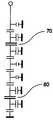
- FIG. 2shows a plurality of stacked FETs of a DTC circuit coupled in series.
- FIG. 3shows a detail of the circuit of FIG. 2 without MIM capacitors.
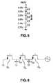
- FIG. 4shows an equivalent circuit of the circuit of FIG. 3 with OFF capacitances in an ideal condition, where the voltage difference is equally divided among the transistors.
- FIG. 5shows a circuit where parasitic capacitances are present.
- FIGS. 6 and 8show stacks of three and sixteen transistors, respectively, with parasitic capacitances.
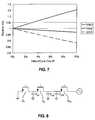
- FIGS. 7 , 9 and 10are waveforms showing the reduced efficiencies of a stack of capacitors in presence of parasitic capacitances.
- FIGS. 11-13show embodiments where compensation capacitors are present.
- FIG. 14shows a stack of OFF capacitances of a DTC with a MIM capacitor on top of the stack.
- FIGS. 15-17show behavior of asymmetric stack in presence of a reactive load.
- FIGS. 18-20show behavior of a symmetric stack in presence of a reactive load.
- FIG. 21shows a stack of ON resistances and ON parasitic capacitances of a DTC with a MIM capacitor on top of the stack.
- FIG. 22shows a stack of OFF capacitances and OFF parasitic capacitances of a DTC.
- FIG. 23shows a diagram where the capacitance of the circuit of FIG. 1 is measured as a function of the various states that the circuit of FIG. 1 can assume when driven at either RF+ or RF ⁇ .
- FIG. 24shows diagrams indicating capacitance asymmetry depending on the polarity of the circuit of FIG. 1 , i.e. whether the circuit is RF+ driven or RF ⁇ driven.
- FIG. 25shows a stack of OFF capacitances of digitally tunable capacitors (DTC) with metal-insulator-metal (MIM) capacitors in the middle of the stack.
- DTCdigitally tunable capacitors
- MIMmetal-insulator-metal
- FIG. 26shows an equivalent circuit with ON resistances and ON parasitic capacitances of a DTC with MIM capacitors in the middle of the stack.
- FIG. 27shows a stack of OFF capacitances and parasitic capacitances of a DTC with MIM capacitors both on the top and the bottom of the stack, thus providing a symmetrical configuration.
- FIG. 28shows a further symmetrical configuration of a stack of OFF capacitances and parasitic capacitances of a DTC including MIM capacitors.
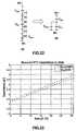
- FIG. 29shows a diagram where the capacitance of the circuit of FIG. 1 is measured as a function of the various states that the circuit of FIG. 1 can assume and as a function of the location of the MIM capacitors.
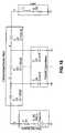
- FIG. 30shows a table where the four stack configurations of FIG. 10 are analyzed in terms of ideal voltage distribution and real voltage distribution due to the presence of parasitic capacitances.
- FIG. 31shows a circuital diagram in accordance with a further embodiment of the disclosure.
- FIGS. 32 and 33show examples of layouts in order to implement the circuital diagram of FIG. 31 .
- FIG. 34shows a circuital diagram in accordance with a further embodiment of the disclosure.
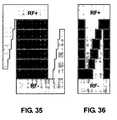
- FIGS. 35 and 36show examples of layouts in order to implement the circuital diagram of FIG. 34 .
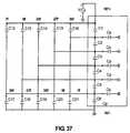
- FIG. 37shows a circuital diagram in accordance with a further embodiment of the disclosure.
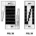
- FIGS. 38 and 39show examples of layouts in order to implement the circuital diagram of FIG. 37 .
- FIGS. 40 and 41show an embodiment where size of the elements of the stack is varied.
- FIG. 1corresponds to FIG. 5D of PCT Patent Application No PCT/US2009/001358 incorporated herein by reference in its entirety.
- FIG. 1is an equivalent circuit showing the ON resistances and OFF capacitances associated with switching FETs of a digitally tunable capacitor (DTC) circuit disclosed in PCT Patent Application PCT/US2009/001358.
- DTCdigitally tunable capacitor
- FIG. 2shows design details of an embodiment of a DTC where a plurality of stacking FETs are coupled in series with associated and corresponding metal-insulator-metal (MIM) or metal-metal (MM) capacitors.
- MIMmetal-insulator-metal
- MMmetal-metal
- FIG. 3represents a detail of the circuit of FIG. 2 without MIM (or MM) capacitors
- FIG. 4shows an equivalent circuit of the circuit of FIG. 3 where all FETs of the FET stack are OFF.
- the voltage at the top of the stackis, for example, 24 V and the voltage at the bottom of the stack is, for example, ground
- the voltage differenceis equally divided among the transistors.
- This ideal conditionis represented in FIG. 4 by showing a voltage drop of 4 V across each OFF capacitance C OFF .
- the voltagesare the peak values of a sinusoidal signal.
- the stack height for this stackwould be 6, because there are 6 devices in series. In this case, there is equal voltage division across the stack so in order to get the voltage across a device one would divide the source voltage by 6.
- FIG. 5shows a simplistic representation of such capacitances to ground, the presence of which does not allow an equal division of the voltage difference across the transistors, thus reducing the efficiency of the stack.
- a possible figure of merit for asymmetric voltage divisionis the effective stack height which is Vsource/Vmax.
- Vmaxis the voltage across the FET closest to the source when the given Vsource is applied.
- the parasitic capacitances of FIG. 5go to ground, the parasitic capacitances from the internal nodes can go to any number of places. In a standard CMOS they may go to the substrate. In an SOI or GaAs process they may go to the package or metal on the back of the part. Parasitic capacitances can also go to nearby metal lines which may also have signal content on them. However, they all include capacitance from an internal node to some other node and can be fairly modeled through the representation of FIG. 5 .
- FIGS. 7 and 9show relative Vds as a function of parasitic capacitance.
- Relative Vdsis defined as the actual voltage across the FET in the presence of parasitics divided by the voltage across the FET if there were no parasitic.
- FIG. 10shows the reduced efficiencies of a stack of capacitors in presence of parasitic capacitances.
- FIG. 7refers to the stack of 3 transistors of FIG. 6
- FIGS. 9 and 10refer to the stack of 16 transistors of FIG. 8 .
- FIG. 7shows relative Vds of transistors as a function of a ratio of Cp to Cds-off in the exemplary stack of three transistors of FIG. 6 . As Cp becomes appreciable in comparison to Cds-off, there is no longer equal voltage division in the stack (Relative Vds diverges from unity).
- FIG. 9shows what happens for the exemplary stack of 16 transistors of FIG. 8 .
- Much smaller ratios of Cp to Cds-offcan make very significant voltage asymmetries through the stack. For example, when Cp is just 1.6% of Cds-off, there is twice as much voltage across transistor 16 as would be expected without parasitic capacitances.
- a stack of 16 transistors with parasitic capacitancesis operating equivalent to a stack of 8 transistors without parasitic capacitances, but at the cost of four times more device area.
- FIG. 10shows the effect of parasitic capacitances on the efficiency of the stack of FIG. 8 .
- the stackWith little or no parasitic capacitances compared to Cds-off, the stack operates as expected. As the ratio of the parasitic capacitance to Cds-off increases, the top transistor in the stack (i.e. the transistor nearest the voltage source) typically sees much more Vds than the rest of the transistors, and the transistors no longer equally share the source voltage. This reduces the stack efficiency. For a stack of 16, ideally the breakdown of the stack would be 16 ⁇ BVds (where BVds is the breakdown voltage of the transistor), but at a Cp/Cds-off ratio of 1.6% (0.016), it will breakdown at 8 ⁇ BVds as shown in FIG. 10 . Thus, at a given ratio of parasitic capacitance Cp to Cds-off for a given process, there is a limit to the maximum stack height.
- Embodiments of the present disclosureare directed at solving the above mentioned problems by adding compensation capacitors across the drain and source of at least the top FETs of the stack closest to the voltage source to decrease asymmetric voltage division.
- FIGS. 11 and 12show a simplified model of a stack with three FETs (already shown in FIG. 6 ) which will be used for purposes of the calculation below, where Cb 2 and Cb 3 represent the compensation capacitors in accordance with the present disclosure.
- Cb 2would have to be equal Cp 1 .
- the capacitance looking left of node 2would be (Cds-off+Cp 1 )/2, assuming all Cds-off are the same.
- the total effective Cds of Q 3would have to be equal to twice that of Cp 1 and the capacitance to the left of it.
- Cb 3Cp 1 +2 Cp 2
- parasitic capacitancescan go to any node in the stack or signal related nodes.
- node N 1would have capacitance to N 2 called Cp 12 , to N 3 called Cp 13 , and so on.
- N 2called Cp 12
- N 3called Cp 13
- Pis the total number of capacitors on node j
- Cijis the total capacitance between node i (N i ) and node j (N j ) which includes parasitic capacitance, compensation capacitance previously added on other nodes, and device Cds-off capacitance.
- FIG. 13shows an embodiment with a stack of six transistors, where compensation capacitors of 45, 30, 18, 9 and 3 fF are used. It should be noted that the effective stack height is back to its ideal value of 6.
- N ⁇ 1 capacitorscan be used to achieve perfect symmetry.
- embodimentsare also possible where less than N ⁇ 1 capacitors are added, starting with the transistor closest to the voltage source (top capacitor of the stack in FIG. 5 , or transistor Q 3 in FIG. 11 ), to improve the effective stack height while not necessarily attaining equal voltage division.
- a further embodiment of the present disclosureis directed at compensation for parasitics by sizing the devices rather than adding compensation capacitance across the drain and source of the FETs.
- the Coff of a deviceis usually linearly related to the size of the device. By putting larger devices closer to the voltage source, the effects of parasitics can be reduced. Reference can be made, for example, to FIGS. 40 and 41 .
- FIG. 41shows how variation of the size of the devices can be obtained. Care should be taken in noting the increase in parasitics due to the increase of the size of the devices. Compensating this way has the benefit of not introducing the process variation of the compensation capacitors (such as MIM) which can be substantial and unrelated to FET Coff process variation.
- Embodiments of the present disclosurecan be provided where the stacked switches are sized so that the first switch (the one closest to the terminal connected to the source) has the same size of the last switch (the one farthest from the terminal connected to the source).
- the second switchhas the same size of the one before last, and so on.
- the sized first and n-th switchescan be larger than the sized second and (n ⁇ 1)-th switches, and so on.
- FIG. 14shows a representation of OFF capacitances ( 20 ) in a stacked configuration where parasitic capacitances ( 30 ) are present and where a MIM capacitor ( 40 ) is shown on top of the stack.
- MIM capacitorsare switched in and out of the circuit using the switch FETs. When the switch FETs are ON, the capacitance of the stack is determined by the MIM capacitor. When the switch FETs are OFF, the capacitance of the stack is reduced by presence of the OFF capacitance. Therefore, the MIM capacitors determine the upper limit of the capacitance tuning range.
- the embodiment shown in FIG. 11can be extended to the case of stacks with MIMs.
- the MIMwill drop some of the voltage, reducing the voltage across the FETs.
- Compensation capacitancecan still be added to the devices to achieve equal voltage division across the FETs only.
- the effective Coffis increased reducing its impedance. It can be noted that adding compensation capacitance has little effect on the circuit performance when the FETs are on due to the relatively small values for Ron.
- compensation capacitorscan be used on all devices and increased without bound hypothetically until the majority of the voltage is dropped across the MIM.
- embodiments of the present applicationspecify the presence of a first RF terminal and a second RF terminal.
- embodiments of the present disclosureare also directed to the presence of terminals which are not RF terminals.
- switchessuch as FET switches.
- elements different from switchessuch as inductors, resistors, capacitors, diodes and so on
- switchescan be provided and the teachings of the present disclosure can be applied to these embodiments as well.
- DTCsdigitally tuned capacitors
- teachings of the present disclosurecan be applied to fields where stacked devices are used different from the field of DTCs, such as switches or attenuators.
- the stackcan be used in applications where none of the terminals RF+ or RF ⁇ is grounded, e.g., using the DTC in series.
- the above compensation schemesare not bidirectional and are effective only if the stack is driven with the voltage source as shown in the above figures and not vice versa.
- such schemesare effective if the RF ⁇ terminal (or the Q 1 source terminal in FIG. 11 ) is either matched or grounded. If RF ⁇ is not matched when RF+ is driven (Q 3 drain in FIG.
- FIGS. 15-17show the above problem and illustrate how voltage divides across an asymmetrically compensated stack when under mismatched load conditions.
- V 12voltage across C 1
- V 23voltage across C 2
- V 34voltage across C 3
- the values C 2 , C 3represent the combined Cds ⁇ OFF+Cb capacitances, similarly to what shown in FIG. 12 .
- the present disclosureovercomes the above problem by providing embodiments according to which the bottom compensation capacitors have the same value of the top compensation capacitors. More generally, assuming that the devices do not have the same Coff, embodiments are provided where compensation capacitances are provided so that the resulting capacitance of the compensated devices is such that the values of such resulting capacitances are symmetrical with respect to the center of the stack. In other words, the stack is symmetrically compensated. For example, with reference to the exemplary scheme of FIG. 13 , and assuming that the Coff of the switches are the same, this would mean that the capacitance value of the compensation capacitors, from top to bottom, would be 45, 30, 18, 30 and 45 fF.
- FIGS. 18-20where a symmetric scheme is shown.
- a symmetric schemeis provided, where the ‘top’ (nearest to the source) capacitance C 1 has the same value of the ‘bottom’ (farthest from the source) capacitance C 3 .
- the waveforms of FIGS. 19 and 20show how V 12 , V 23 and V 34 are almost identical to each other.
- comparison between FIG. 17 and FIG. 20shows the advantage of adopting a symmetrical arrangement in cases with a reactive load.
- FIG. 14see also FIG. 21 ).
- placement of the MIM capacitors ( 40 ) across the FET stack in presence of parasitic capacitancecan make the tunable capacitor stack non-reciprocal.
- the stack shown in FIG. 14is not bi-directional in the sense that the effective capacitance and voltage handling differs depending on the port (RF+ or RF ⁇ ) being driven.
- FIGS. 21 and 22show simplified equivalent circuits of the stack of FETs, where the FETs are in an ON condition ( FIG. 21 ) or in an OFF condition ( FIG. 22 ).
- parasitic capacitances Cpon ( 50 )are present to a ground node, and the stack in the ON condition can be represented by the equivalent circuit shown in FIG. 21( b ).
- the ON condition of FIGS. 21( a ) and 21 ( b )when driving RF+, the parasitic capacitance Cpon is not seen because the impedance of Ron is much lower than the impedance of Cpon.
- Cponappears in parallel with CMIM, thus increasing the effective capacitance. Therefore, in the ON condition, presence of the parasitic capacitances Cpon, although not necessarily a problem, can be a source of non-bidirectionality.
- FIGS. 22( a ) and 22 ( b )show a stack or arm of FET transistors with a MIM or MM capacitor on top in the OFF condition, where the circuit of FIG. 22( b ) is the simplified circuital equivalent of the OFF arm of FIG. 22( a ).
- the effective capacitance seenis different from the capacitance seen when driving RF ⁇ .
- Such undesired differencecan be explained, for example, with reference to the diagram of FIG. 23 .
- FIG. 23shows a diagram where the capacitance of the circuit of FIG. 1 is measured as a function of the various states that the circuit of FIG. 1 can assume.
- the 5-bit circuit of FIG. 1can assume 32 states from 00000 (state 0 , which corresponds to all bits being in the OFF state as shown in FIG. 22 ) to 11111 (state 31 , which corresponds to all bits being in the ON state as shown in FIG. 21 ).
- the capacitance of the circuit for each stateis represented in FIG. 23 for each of the 32 states.
- the top line of dots of FIG. 23represents values where RF ⁇ is driven (shunt RF ⁇ ), while the bottom line of dots of FIG. 23 represents values where RF+ is driven (shunt RF+).
- the difference in capacitance value for each stateis a clear indication of the lack of bi-directionality of the circuit of FIG. 1 because of the presence of an offset due to the presence of a parasitic C term.
- FIG. 24shows diagrams indicating, in detail, the asymmetry of the DTC capacitance depending on the polarity in the shunt, i.e. whether the circuit is RF+ driven or RF ⁇ driven.
- FIG. 24( a )shows that there is a non-monotonicity of the capacitance values in the shunt RF ⁇ case, meaning that the capacitance for state 16 has a value that is inferior to the value for state 15 .
- Such lack of monotonicityrepresents a problem, especially in closed loop applications.
- FIGS. 24( b ) and 24 ( c )where differential linearity (DNL) and integral linearity (INL) signals are shown.
- DNLrepresents the actual step size versus the ideal step size
- INLrepresents the difference between capacitance values and a reference straight line drawn through the end points.
- both DNL and INLshould be equal to zero across the various states.
- the diagrams of FIGS. 24( b ) and 24 ( c )show that the Shunt RF+ condition (circuit RF+ driven) of FIG. 24( c ), although not ideal, is much better than the Shunt RF ⁇ condition (circuit RF ⁇ driven) of FIG. 24( b ) where there is a large discrepancy between the ideal and real values of DNL and INL.
- a first embodiment of the present disclosure to solve the above mentioned problemis shown in the circuit of FIG. 25 , where MIM or MM capacitor ( 60 ) is placed in the middle of the stack. See also FIGS. 26( a )- 26 ( c ).
- MIM capacitor ( 60 ) in the middleneither eliminates nor compensates the parasitic capacitance Cp. Rather, the parasitic capacitances are now symmetric about the MIM capacitor, so that the RF+ and RF ⁇ mirror each other both in the ON state and in the OFF state. Therefore, such embodiment eliminates asymmetries in the DTC capacitance, thus allowing the same capacitance value to be obtained whether driving RF+ or RF ⁇ .
- placement of a single MINI capacitor in the middle of the stackcan not be advisable due to breakdown voltage limitations of the MIM capacitor.
- two or more MIM capacitorscan be provided in series, to overcome such limitations.
- MIM capacitorscan be placed in a variety of positions as long as they are symmetrical with respect to the center of the stack.
- one possible placementcould be to double the MIM capacitance and put one on each end of the stack, as shown in FIG. 27 .
- the MIM capacitanceshave been doubled, as shown in the figure.
- FIG. 28shows a further embodiment of the present disclosure where MIM capacitors ( 70 , 80 ) have been placed in positions that provide an overall symmetrical configuration.
- FIG. 29shows a further capacitance vs. state diagram, this time with reference to five different scenarios: 1) ideal (first line from the bottom), assuming no parasitic C to ground 2) MIM at the RF+ end (second line from the bottom); 3) MIM at both ends (third line from the bottom); 4) MIM in the middle (fourth line from the bottom); and 5) MIM at the RF ⁇ end (fifth line from the bottom, first from the top).
- the diagram of FIG. 29shows how for a typical scenario, the capacitance for the MIM at one end approach depends strongly on which end is driven (see distance between line 2 and line 5 ), while the symmetric approach is bilateral and closer to ideal.
- FIG. 30shows a table similar to the diagram of FIG. 29 .
- FIG. 30shows the effects of MIM placement on voltage division.
- the columns with the ‘Parasitics’ headertake into account the parasitic C to ground.
- the last row (Max Vpk)is the maximum voltage capability of each configuration. It can be noted that the embodiment with MIM at the top and the embodiment with MIM at the bottom give different results, which is not desired because it means that the configuration is not bi-directional. It should also be noted that the table of FIG. 30 does not include any compensation.
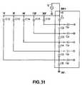
- FIG. 31shows a further embodiment of the present disclosure.
- a stack of devices showing Coff capacitances C 1 . . . C 6 and respective parasitic capacitances as mentioned aboveis shown.
- compensation capacitances C 12 . . . C 16are provided.
- a first compensation capacitance C 16is provided across (in parallel with) the first device
- a second compensation capacitance C 15is provided across the series of the first and second device
- a third compensation capacitance C 14is provided across the series of the first, second and third device, and so on.
- the last compensation capacitanceis provided across the series of all devices with the exclusion of the device farthest from the source (n-th device).
- FIGS. 32 and 33show exemplary layouts of the compensation capacitors in accordance with the embodiment of FIG. 31 , where Metal-Metal (MM) compensation capacitors are used, by way of example.
- FIGS. 32 and 33are views from the top of the stack of switches (disposed, e.g., in an interdigitated manner where the source of each switch is interdigitated with the drain of the device) disposed between the first terminal RF+ and the second terminal RF ⁇ .
- a capacitive effectis obtained by adding metal to the side of the switches in a controlled amount and at a controlled distance from each switch to obtain a controlled capacitive metal-insulator-metal effect between the RF+ node and each node of the stack. It should be noted how, in FIG. 32 , the distance between the added metal and the stacked devices is variable (the larger the distance the lower the capacitance), to obtained a controllable capacitance effect.
- the metalis added on top of the switches along a substantially central region of the same.
- the variable capacitive effectis obtained through control of the amount of metal deposited on the top of each switch.
- FIG. 34shows another embodiment of the present disclosure, similar to the embodiment of FIG. 31 .
- the embodiment of FIG. 34shows additional compensation capacitances C 17 . . . C 21 .
- a first additional compensation capacitance C 17is provided across (in parallel with) the last (n-th) device
- a second compensation capacitance C 18is provided across the series of the n-th and (n ⁇ 1)-th device
- a third compensation capacitance C 17is provided across the series of the n-th, (n ⁇ 1)-th and (n ⁇ 2)-th device, and so on.
- the last additional compensation capacitanceis provided across the series of all devices with the exclusion of the device closest to the source (1 st device).
- n ⁇ 1) compensating capacitorscan be provided on each side of the stack for each embodiment, each embodiment comprising compensating capacitors located across the first device, the series of the first and second device, the series of the first, second and third device, up to the series of all devices from the first device to the i-th device, and corresponding compensating capacitors located across the n-th device, the series of the n-th and (n ⁇ 1)-th device, the series of the n-th, (n ⁇ 1)-th and (n ⁇ 2)-th device, up to the series of all devices from the first device to the (n ⁇ i+1)-th device.
- FIGS. 35 and 36show exemplary layouts of the compensation capacitors in accordance with the embodiment of FIG. 34 .
- the metalis added on the side or on top of the switches similarly to the embodiment of FIGS. 32 and 33 .
- FIG. 37shows a further embodiment of the present disclosure, similar to the embodiment of FIG. 34 .
- the compensationis symmetric.
- Each compensating capacitor on the top of the figurehas a corresponding compensating capacitor on the bottom of the figure so that the resulting capacitance value on the top of the stack is the same as the resulting capacitance value on the bottom of the stack.
- the resulting capacitance value between the first and the second node (36 pF)is the same as the resulting capacitance value between the n-th and the (n ⁇ 1)-th node.
- the resulting capacitance value between the first and the third node (27 pF)is the same as the resulting capacitance value between the n-th and the (n ⁇ 2)-th node, and so on.
- FIGS. 38 and 39show exemplary layouts of the compensation capacitors in accordance with the embodiment of FIG. 37 .
- the metalis added on the side or on top of the switches similarly to the embodiment of FIGS. 35 and 36 .
Landscapes
- Engineering & Computer Science (AREA)
- Power Engineering (AREA)
- Microelectronics & Electronic Packaging (AREA)
- Physics & Mathematics (AREA)
- Theoretical Computer Science (AREA)
- Nonlinear Science (AREA)
- General Physics & Mathematics (AREA)
- Computer Hardware Design (AREA)
- Condensed Matter Physics & Semiconductors (AREA)
- Manufacturing & Machinery (AREA)
- Semiconductor Integrated Circuits (AREA)
- Amplifiers (AREA)
- Filters And Equalizers (AREA)
Abstract
Description
Cds3−eff=2×((Cds-off+Cp1)/2+Cp2)=Cds-off+Cp1+2Cp2
Thus,Cb3=Cp1+2Cp2
assuming that all transistors have the same Cds-off.
where:
P is the total number of capacitors on node j; and
Cij is the total capacitance between node i (Ni) and node j (Nj) which includes parasitic capacitance, compensation capacitance previously added on other nodes, and device Cds-off capacitance.
where S is the integer number of transistors in the stack.
Claims (15)
Priority Applications (5)
| Application Number | Priority Date | Filing Date | Title |
|---|---|---|---|
| US12/803,064US8638159B2 (en) | 2008-02-28 | 2010-06-18 | Devices and methods for improving voltage handling and/or bi-directionality of stacks of elements when connected between terminals |
| US14/165,422US9496849B2 (en) | 2008-02-28 | 2014-01-27 | Devices and methods for improving voltage handling and/or bi-directionality of stacks of elements when connected between terminals |
| US14/178,116US9106227B2 (en) | 2008-02-28 | 2014-02-11 | Devices and methods for improving voltage handling and/or bi-directionality of stacks of elements when connected between terminals |
| US14/814,404US9755615B2 (en) | 2008-02-28 | 2015-07-30 | Devices and methods for improving voltage handling and/or bi-directionality of stacks of elements when connected between terminals |
| US15/442,491US10050616B2 (en) | 2008-02-28 | 2017-02-24 | Devices and methods for improving voltage handling and/or bi-directionality of stacks of elements when connected between terminals |
Applications Claiming Priority (3)
| Application Number | Priority Date | Filing Date | Title |
|---|---|---|---|
| US6763408P | 2008-02-28 | 2008-02-28 | |
| PCT/US2009/001358WO2009108391A1 (en) | 2008-02-28 | 2009-03-02 | Method and apparatus for use in digitally tuning a capacitor in an integrated circuit device |
| US12/803,064US8638159B2 (en) | 2008-02-28 | 2010-06-18 | Devices and methods for improving voltage handling and/or bi-directionality of stacks of elements when connected between terminals |
Related Parent Applications (2)
| Application Number | Title | Priority Date | Filing Date |
|---|---|---|---|
| PCT/US2009/001358Continuation-In-PartWO2009108391A1 (en) | 2008-02-28 | 2009-03-02 | Method and apparatus for use in digitally tuning a capacitor in an integrated circuit device |
| PCT/US2009/001358ContinuationWO2009108391A1 (en) | 2008-02-28 | 2009-03-02 | Method and apparatus for use in digitally tuning a capacitor in an integrated circuit device |
Related Child Applications (1)
| Application Number | Title | Priority Date | Filing Date |
|---|---|---|---|
| US14/165,422ContinuationUS9496849B2 (en) | 2008-02-28 | 2014-01-27 | Devices and methods for improving voltage handling and/or bi-directionality of stacks of elements when connected between terminals |
Publications (2)
| Publication Number | Publication Date |
|---|---|
| US20110043271A1 US20110043271A1 (en) | 2011-02-24 |
| US8638159B2true US8638159B2 (en) | 2014-01-28 |
Family
ID=41016424
Family Applications (24)
| Application Number | Title | Priority Date | Filing Date |
|---|---|---|---|
| US12/735,954ActiveUS9024700B2 (en) | 2008-02-28 | 2009-03-02 | Method and apparatus for use in digitally tuning a capacitor in an integrated circuit device |
| US12/803,133Active2029-05-11US8604864B2 (en) | 2008-02-28 | 2010-06-18 | Devices and methods for improving voltage handling and/or bi-directionality of stacks of elements when connected between terminals |
| US12/803,139Active2031-04-25US8669804B2 (en) | 2008-02-28 | 2010-06-18 | Devices and methods for improving voltage handling and/or bi-directionality of stacks of elements when connected between terminals |
| US12/803,064ActiveUS8638159B2 (en) | 2008-02-28 | 2010-06-18 | Devices and methods for improving voltage handling and/or bi-directionality of stacks of elements when connected between terminals |
| US13/586,738Active2030-01-12US9293262B2 (en) | 2008-02-28 | 2012-08-15 | Digitally tuned capacitors with tapered and reconfigurable quality factors |
| US13/595,893Active2029-11-06US9197194B2 (en) | 2008-02-28 | 2012-08-27 | Methods and apparatuses for use in tuning reactance in a circuit device |
| US14/165,422Active2029-07-08US9496849B2 (en) | 2008-02-28 | 2014-01-27 | Devices and methods for improving voltage handling and/or bi-directionality of stacks of elements when connected between terminals |
| US14/178,116ActiveUS9106227B2 (en) | 2008-02-28 | 2014-02-11 | Devices and methods for improving voltage handling and/or bi-directionality of stacks of elements when connected between terminals |
| US14/638,917Active2029-06-30US9667227B2 (en) | 2008-02-28 | 2015-03-04 | Method and apparatus for use in digitally tuning a capacitor in an integrated circuit device |
| US14/814,404ActiveUS9755615B2 (en) | 2008-02-28 | 2015-07-30 | Devices and methods for improving voltage handling and/or bi-directionality of stacks of elements when connected between terminals |
| US14/883,512ActiveUS9806694B2 (en) | 2008-02-28 | 2015-10-14 | Methods and apparatuses for use in tuning reactance in a circuit device |
| US15/279,302Active2030-01-24US10382031B2 (en) | 2008-02-28 | 2016-09-28 | Method and apparatus for use in digitally tuning a capacitor in an integrated circuit device |
| US15/442,491ActiveUS10050616B2 (en) | 2008-02-28 | 2017-02-24 | Devices and methods for improving voltage handling and/or bi-directionality of stacks of elements when connected between terminals |
| US15/688,658ActiveUS10158345B2 (en) | 2008-02-28 | 2017-08-28 | Methods and apparatuses for use in tuning reactance in a circuit device |
| US16/025,922ActiveUS10630284B2 (en) | 2008-02-28 | 2018-07-02 | Devices and methods for improving voltage handling and/or bi-directionality of stacks of elements when connected between terminals |
| US16/156,930AbandonedUS20190123735A1 (en) | 2008-02-28 | 2018-10-10 | Methods and Apparatuses for Use in Tuning Reactance in a Circuit Device |
| US16/524,710ActiveUS11258440B2 (en) | 2008-02-28 | 2019-07-29 | Method and apparatus for use in digitally tuning a capacitor in an integrated circuit device |
| US16/837,758ActiveUS11082040B2 (en) | 2008-02-28 | 2020-04-01 | Devices and methods for improving voltage handling and/or bi-directionality of stacks of elements when connected between terminals |
| US17/078,658ActiveUS11606087B2 (en) | 2008-02-28 | 2020-10-23 | Methods and apparatuses for use in tuning reactance in a circuit device |
| US17/387,469ActiveUS11671091B2 (en) | 2008-02-28 | 2021-07-28 | Devices and methods for improving voltage handling and/or bi-directionality of stacks of elements when connected between terminals |
| US17/674,370Active2029-12-14US12199599B2 (en) | 2008-02-28 | 2022-02-17 | Method and apparatus for use in digitally tuning a capacitor in an integrated circuit device |
| US18/182,326ActiveUS12425016B2 (en) | 2008-02-28 | 2023-03-11 | Methods and apparatuses for use in tuning reactance in a circuit device |
| US18/328,251Active2029-06-04US12431890B2 (en) | 2008-02-28 | 2023-06-02 | Devices and methods for improving voltage handling and/or bi-directionality of stacks of elements when connected between terminals |
| US18/968,917PendingUS20250132759A1 (en) | 2008-02-28 | 2024-12-04 | Method And Apparatus For Use In Digitally Tuning A Capacitor In An Integrated Circuit Device |
Family Applications Before (3)
| Application Number | Title | Priority Date | Filing Date |
|---|---|---|---|
| US12/735,954ActiveUS9024700B2 (en) | 2008-02-28 | 2009-03-02 | Method and apparatus for use in digitally tuning a capacitor in an integrated circuit device |
| US12/803,133Active2029-05-11US8604864B2 (en) | 2008-02-28 | 2010-06-18 | Devices and methods for improving voltage handling and/or bi-directionality of stacks of elements when connected between terminals |
| US12/803,139Active2031-04-25US8669804B2 (en) | 2008-02-28 | 2010-06-18 | Devices and methods for improving voltage handling and/or bi-directionality of stacks of elements when connected between terminals |
Family Applications After (20)
| Application Number | Title | Priority Date | Filing Date |
|---|---|---|---|
| US13/586,738Active2030-01-12US9293262B2 (en) | 2008-02-28 | 2012-08-15 | Digitally tuned capacitors with tapered and reconfigurable quality factors |
| US13/595,893Active2029-11-06US9197194B2 (en) | 2008-02-28 | 2012-08-27 | Methods and apparatuses for use in tuning reactance in a circuit device |
| US14/165,422Active2029-07-08US9496849B2 (en) | 2008-02-28 | 2014-01-27 | Devices and methods for improving voltage handling and/or bi-directionality of stacks of elements when connected between terminals |
| US14/178,116ActiveUS9106227B2 (en) | 2008-02-28 | 2014-02-11 | Devices and methods for improving voltage handling and/or bi-directionality of stacks of elements when connected between terminals |
| US14/638,917Active2029-06-30US9667227B2 (en) | 2008-02-28 | 2015-03-04 | Method and apparatus for use in digitally tuning a capacitor in an integrated circuit device |
| US14/814,404ActiveUS9755615B2 (en) | 2008-02-28 | 2015-07-30 | Devices and methods for improving voltage handling and/or bi-directionality of stacks of elements when connected between terminals |
| US14/883,512ActiveUS9806694B2 (en) | 2008-02-28 | 2015-10-14 | Methods and apparatuses for use in tuning reactance in a circuit device |
| US15/279,302Active2030-01-24US10382031B2 (en) | 2008-02-28 | 2016-09-28 | Method and apparatus for use in digitally tuning a capacitor in an integrated circuit device |
| US15/442,491ActiveUS10050616B2 (en) | 2008-02-28 | 2017-02-24 | Devices and methods for improving voltage handling and/or bi-directionality of stacks of elements when connected between terminals |
| US15/688,658ActiveUS10158345B2 (en) | 2008-02-28 | 2017-08-28 | Methods and apparatuses for use in tuning reactance in a circuit device |
| US16/025,922ActiveUS10630284B2 (en) | 2008-02-28 | 2018-07-02 | Devices and methods for improving voltage handling and/or bi-directionality of stacks of elements when connected between terminals |
| US16/156,930AbandonedUS20190123735A1 (en) | 2008-02-28 | 2018-10-10 | Methods and Apparatuses for Use in Tuning Reactance in a Circuit Device |
| US16/524,710ActiveUS11258440B2 (en) | 2008-02-28 | 2019-07-29 | Method and apparatus for use in digitally tuning a capacitor in an integrated circuit device |
| US16/837,758ActiveUS11082040B2 (en) | 2008-02-28 | 2020-04-01 | Devices and methods for improving voltage handling and/or bi-directionality of stacks of elements when connected between terminals |
| US17/078,658ActiveUS11606087B2 (en) | 2008-02-28 | 2020-10-23 | Methods and apparatuses for use in tuning reactance in a circuit device |
| US17/387,469ActiveUS11671091B2 (en) | 2008-02-28 | 2021-07-28 | Devices and methods for improving voltage handling and/or bi-directionality of stacks of elements when connected between terminals |
| US17/674,370Active2029-12-14US12199599B2 (en) | 2008-02-28 | 2022-02-17 | Method and apparatus for use in digitally tuning a capacitor in an integrated circuit device |
| US18/182,326ActiveUS12425016B2 (en) | 2008-02-28 | 2023-03-11 | Methods and apparatuses for use in tuning reactance in a circuit device |
| US18/328,251Active2029-06-04US12431890B2 (en) | 2008-02-28 | 2023-06-02 | Devices and methods for improving voltage handling and/or bi-directionality of stacks of elements when connected between terminals |
| US18/968,917PendingUS20250132759A1 (en) | 2008-02-28 | 2024-12-04 | Method And Apparatus For Use In Digitally Tuning A Capacitor In An Integrated Circuit Device |
Country Status (4)
| Country | Link |
|---|---|
| US (24) | US9024700B2 (en) |
| EP (5) | EP3346611B1 (en) |
| JP (5) | JP5417346B2 (en) |
| WO (1) | WO2009108391A1 (en) |
Cited By (47)
| Publication number | Priority date | Publication date | Assignee | Title |
|---|---|---|---|---|
| US20140340181A1 (en)* | 2013-05-14 | 2014-11-20 | Infineon Technologies Ag | System and Method for a Switchable Capacitance |
| US9024700B2 (en) | 2008-02-28 | 2015-05-05 | Peregrine Semiconductor Corporation | Method and apparatus for use in digitally tuning a capacitor in an integrated circuit device |
| US9177737B2 (en) | 2007-04-26 | 2015-11-03 | Peregrine Semiconductor Corporation | Tuning capacitance to enhance FET stack voltage withstand |
| US9196459B2 (en) | 2014-01-10 | 2015-11-24 | Reno Technologies, Inc. | RF impedance matching network |
| US9306533B1 (en) | 2015-02-20 | 2016-04-05 | Reno Technologies, Inc. | RF impedance matching network |
| US9496122B1 (en) | 2014-01-10 | 2016-11-15 | Reno Technologies, Inc. | Electronically variable capacitor and RF matching network incorporating same |
| US9525412B2 (en) | 2015-02-18 | 2016-12-20 | Reno Technologies, Inc. | Switching circuit |
| US9697991B2 (en) | 2014-01-10 | 2017-07-04 | Reno Technologies, Inc. | RF impedance matching network |
| US9729122B2 (en) | 2015-02-18 | 2017-08-08 | Reno Technologies, Inc. | Switching circuit |
| US9755641B1 (en) | 2014-01-10 | 2017-09-05 | Reno Technologies, Inc. | High speed high voltage switching circuit |
| US20170323881A1 (en)* | 2016-05-03 | 2017-11-09 | Infineon Technologies Ag | Switch Having First and Second Switching Elements Connected in Parallel with One Another |
| US9831857B2 (en) | 2015-03-11 | 2017-11-28 | Peregrine Semiconductor Corporation | Power splitter with programmable output phase shift |
| US9844127B2 (en) | 2014-01-10 | 2017-12-12 | Reno Technologies, Inc. | High voltage switching circuit |
| US9865432B1 (en) | 2014-01-10 | 2018-01-09 | Reno Technologies, Inc. | RF impedance matching network |
| US9948281B2 (en) | 2016-09-02 | 2018-04-17 | Peregrine Semiconductor Corporation | Positive logic digitally tunable capacitor |
| US10236872B1 (en) | 2018-03-28 | 2019-03-19 | Psemi Corporation | AC coupling modules for bias ladders |
| US10340879B2 (en) | 2015-02-18 | 2019-07-02 | Reno Technologies, Inc. | Switching circuit |
| US10431428B2 (en) | 2014-01-10 | 2019-10-01 | Reno Technologies, Inc. | System for providing variable capacitance |
| US10455729B2 (en) | 2014-01-10 | 2019-10-22 | Reno Technologies, Inc. | Enclosure cooling system |
| US10483090B2 (en) | 2017-07-10 | 2019-11-19 | Reno Technologies, Inc. | Restricted capacitor switching |
| US10505530B2 (en) | 2018-03-28 | 2019-12-10 | Psemi Corporation | Positive logic switch with selectable DC blocking circuit |
| US10692699B2 (en) | 2015-06-29 | 2020-06-23 | Reno Technologies, Inc. | Impedance matching with restricted capacitor switching |
| US10714314B1 (en) | 2017-07-10 | 2020-07-14 | Reno Technologies, Inc. | Impedance matching network and method |
| US10727029B2 (en) | 2017-07-10 | 2020-07-28 | Reno Technologies, Inc | Impedance matching using independent capacitance and frequency control |
| US10886911B2 (en) | 2018-03-28 | 2021-01-05 | Psemi Corporation | Stacked FET switch bias ladders |
| US10984986B2 (en) | 2015-06-29 | 2021-04-20 | Reno Technologies, Inc. | Impedance matching network and method |
| US11049855B2 (en) | 2018-08-09 | 2021-06-29 | Psemi Corporation | Tunable capacitive compensation for RF switch FET stacks |
| US11081316B2 (en) | 2015-06-29 | 2021-08-03 | Reno Technologies, Inc. | Impedance matching network and method |
| US11101110B2 (en) | 2017-07-10 | 2021-08-24 | Reno Technologies, Inc. | Impedance matching network and method |
| US11114280B2 (en) | 2017-07-10 | 2021-09-07 | Reno Technologies, Inc. | Impedance matching with multi-level power setpoint |
| US11150283B2 (en) | 2015-06-29 | 2021-10-19 | Reno Technologies, Inc. | Amplitude and phase detection circuit |
| US11289307B2 (en) | 2017-07-10 | 2022-03-29 | Reno Technologies, Inc. | Impedance matching network and method |
| US11315758B2 (en) | 2017-07-10 | 2022-04-26 | Reno Technologies, Inc. | Impedance matching using electronically variable capacitance and frequency considerations |
| US11335540B2 (en) | 2015-06-29 | 2022-05-17 | Reno Technologies, Inc. | Impedance matching network and method |
| US11342160B2 (en) | 2015-06-29 | 2022-05-24 | Reno Technologies, Inc. | Filter for impedance matching |
| US11342161B2 (en) | 2015-06-29 | 2022-05-24 | Reno Technologies, Inc. | Switching circuit with voltage bias |
| US11393659B2 (en) | 2017-07-10 | 2022-07-19 | Reno Technologies, Inc. | Impedance matching network and method |
| US11398370B2 (en) | 2017-07-10 | 2022-07-26 | Reno Technologies, Inc. | Semiconductor manufacturing using artificial intelligence |
| US11476091B2 (en) | 2017-07-10 | 2022-10-18 | Reno Technologies, Inc. | Impedance matching network for diagnosing plasma chamber |
| US11476849B2 (en) | 2020-01-06 | 2022-10-18 | Psemi Corporation | High power positive logic switch |
| US11521831B2 (en) | 2019-05-21 | 2022-12-06 | Reno Technologies, Inc. | Impedance matching network and method with reduced memory requirements |
| US11521833B2 (en) | 2017-07-10 | 2022-12-06 | Reno Technologies, Inc. | Combined RF generator and RF solid-state matching network |
| US11631570B2 (en) | 2015-02-18 | 2023-04-18 | Reno Technologies, Inc. | Switching circuit |
| US12119206B2 (en) | 2015-02-18 | 2024-10-15 | Asm America, Inc. | Switching circuit |
| US12272522B2 (en) | 2017-07-10 | 2025-04-08 | Asm America, Inc. | Resonant filter for solid state RF impedance matching network |
| US12334307B2 (en) | 2017-07-10 | 2025-06-17 | Asm Ip Holding B.V. | Power control for rf impedance matching network |
| US12444573B2 (en) | 2022-04-18 | 2025-10-14 | Asm America, Inc. | Impedance matching network and method |
Families Citing this family (291)
| Publication number | Priority date | Publication date | Assignee | Title |
|---|---|---|---|---|
| US8744384B2 (en) | 2000-07-20 | 2014-06-03 | Blackberry Limited | Tunable microwave devices with auto-adjusting matching circuit |
| US6804502B2 (en) | 2001-10-10 | 2004-10-12 | Peregrine Semiconductor Corporation | Switch circuit and method of switching radio frequency signals |
| EP3570374B1 (en) | 2004-06-23 | 2022-04-20 | pSemi Corporation | Integrated rf front end |
| US9653601B2 (en) | 2005-07-11 | 2017-05-16 | Peregrine Semiconductor Corporation | Method and apparatus for use in improving linearity of MOSFETs using an accumulated charge sink-harmonic wrinkle reduction |
| US8742502B2 (en) | 2005-07-11 | 2014-06-03 | Peregrine Semiconductor Corporation | Method and apparatus for use in improving linearity of MOSFETs using an accumulated charge sink-harmonic wrinkle reduction |
| USRE48965E1 (en) | 2005-07-11 | 2022-03-08 | Psemi Corporation | Method and apparatus improving gate oxide reliability by controlling accumulated charge |
| US7910993B2 (en) | 2005-07-11 | 2011-03-22 | Peregrine Semiconductor Corporation | Method and apparatus for use in improving linearity of MOSFET's using an accumulated charge sink |
| US7890891B2 (en) | 2005-07-11 | 2011-02-15 | Peregrine Semiconductor Corporation | Method and apparatus improving gate oxide reliability by controlling accumulated charge |
| US20080076371A1 (en)* | 2005-07-11 | 2008-03-27 | Alexander Dribinsky | Circuit and method for controlling charge injection in radio frequency switches |
| US9406444B2 (en) | 2005-11-14 | 2016-08-02 | Blackberry Limited | Thin film capacitors |
| US7711337B2 (en) | 2006-01-14 | 2010-05-04 | Paratek Microwave, Inc. | Adaptive impedance matching module (AIMM) control architectures |
| GB0614037D0 (en)* | 2006-07-14 | 2006-08-23 | Amura Therapeutics Ltd | Compounds |
| US7714676B2 (en) | 2006-11-08 | 2010-05-11 | Paratek Microwave, Inc. | Adaptive impedance matching apparatus, system and method |
| US7535312B2 (en) | 2006-11-08 | 2009-05-19 | Paratek Microwave, Inc. | Adaptive impedance matching apparatus, system and method with improved dynamic range |
| US7917104B2 (en) | 2007-04-23 | 2011-03-29 | Paratek Microwave, Inc. | Techniques for improved adaptive impedance matching |
| US8213886B2 (en) | 2007-05-07 | 2012-07-03 | Paratek Microwave, Inc. | Hybrid techniques for antenna retuning utilizing transmit and receive power information |
| US8058700B1 (en)* | 2007-06-07 | 2011-11-15 | Inpower Llc | Surge overcurrent protection for solid state, smart, highside, high current, power switch |
| US7991363B2 (en) | 2007-11-14 | 2011-08-02 | Paratek Microwave, Inc. | Tuning matching circuits for transmitter and receiver bands as a function of transmitter metrics |
| US9917359B2 (en) | 2008-03-05 | 2018-03-13 | Ethertronics, Inc. | Repeater with multimode antenna |
| US8212541B2 (en) | 2008-05-08 | 2012-07-03 | Massachusetts Institute Of Technology | Power converter with capacitive energy transfer and fast dynamic response |
| US8072285B2 (en) | 2008-09-24 | 2011-12-06 | Paratek Microwave, Inc. | Methods for tuning an adaptive impedance matching network with a look-up table |
| US8395435B2 (en)* | 2009-07-30 | 2013-03-12 | Qualcomm, Incorporated | Switches with bias resistors for even voltage distribution |
| US8472888B2 (en) | 2009-08-25 | 2013-06-25 | Research In Motion Rf, Inc. | Method and apparatus for calibrating a communication device |
| US9026062B2 (en)* | 2009-10-10 | 2015-05-05 | Blackberry Limited | Method and apparatus for managing operations of a communication device |
| DE102010006438A1 (en) | 2010-02-01 | 2011-08-04 | Epcos Ag, 81669 | Switchable capacitive element with improved quality factor and method of manufacture |
| DE102010011411B4 (en) | 2010-03-15 | 2015-07-02 | Qualcomm Technologies, Inc. (N.D.Ges.D. Staates Delaware) | Adjustable capacitive element |
| US8803631B2 (en) | 2010-03-22 | 2014-08-12 | Blackberry Limited | Method and apparatus for adapting a variable impedance network |
| DE102010014101B4 (en) | 2010-04-07 | 2016-06-09 | Epcos Ag | Hybrid circuit with adjustable impedance |
| JP5901612B2 (en) | 2010-04-20 | 2016-04-13 | ブラックベリー リミテッド | Method and apparatus for managing interference in a communication device |
| US9203489B2 (en) | 2010-05-05 | 2015-12-01 | Google Technology Holdings LLC | Method and precoder information feedback in multi-antenna wireless communication systems |
| US8791767B2 (en)* | 2010-10-29 | 2014-07-29 | Qualcomm Incorporated | Package inductance compensating tunable capacitor circuit |
| US9379454B2 (en) | 2010-11-08 | 2016-06-28 | Blackberry Limited | Method and apparatus for tuning antennas in a communication device |
| US10389235B2 (en) | 2011-05-05 | 2019-08-20 | Psemi Corporation | Power converter |
| FR2970129B1 (en)* | 2010-12-30 | 2013-01-18 | Thales Sa | CAPACITOR VARIABLE FILTER SWITCHED USING MEMS COMPONENTS |
| US8712340B2 (en) | 2011-02-18 | 2014-04-29 | Blackberry Limited | Method and apparatus for radio antenna frequency tuning |
| US8655286B2 (en) | 2011-02-25 | 2014-02-18 | Blackberry Limited | Method and apparatus for tuning a communication device |
| EP4318909A3 (en) | 2011-05-05 | 2024-03-06 | PSEMI Corporation | Dc-dc converter with modular stages |
| US10680515B2 (en) | 2011-05-05 | 2020-06-09 | Psemi Corporation | Power converters with modular stages |
| US9882471B2 (en) | 2011-05-05 | 2018-01-30 | Peregrine Semiconductor Corporation | DC-DC converter with modular stages |
| US8594584B2 (en) | 2011-05-16 | 2013-11-26 | Blackberry Limited | Method and apparatus for tuning a communication device |
| EP2740221B1 (en) | 2011-08-05 | 2019-06-26 | BlackBerry Limited | Method and apparatus for band tuning in a communication device |
| US8305139B1 (en)* | 2011-10-05 | 2012-11-06 | Peregrine Semiconductor Corporation | Methods and apparatuses for high power and/or high frequency devices |
| US8743553B2 (en) | 2011-10-18 | 2014-06-03 | Arctic Sand Technologies, Inc. | Power converters with integrated capacitors |
| US8723491B2 (en) | 2011-12-19 | 2014-05-13 | Arctic Sand Technologies, Inc. | Control of power converters with capacitive energy transfer |
| JP5810910B2 (en)* | 2011-12-28 | 2015-11-11 | 富士通株式会社 | Antenna design method, antenna design apparatus, antenna design program |
| US20130187828A1 (en) | 2012-01-24 | 2013-07-25 | Ethertronics, Inc. | Tunable matching network for antenna systems |
| US9002278B2 (en) | 2012-02-29 | 2015-04-07 | Htc Corporation | Simple automatic antenna tuning system and method |
| JP2013197175A (en)* | 2012-03-16 | 2013-09-30 | Samsung Electro-Mechanics Co Ltd | Integrated circuit and radio communication device |
| FR2988239A1 (en)* | 2012-03-16 | 2013-09-20 | Converteam Technology Ltd | METHOD FOR COMPENSATING TOLERANCES FOR MANUFACTURING AT LEAST ONE ELECTRIC PARAMETER OF A POWER TRANSISTOR AND SYSTEM THEREOF |
| KR101350461B1 (en)* | 2012-04-03 | 2014-01-09 | 주식회사 하이딥 | Tunable capacitor |
| KR101338286B1 (en)* | 2012-04-03 | 2013-12-06 | 주식회사 하이딥 | Tunable capacitor |
| US9263793B2 (en) | 2012-04-20 | 2016-02-16 | Ethertronics, Inc. | Multi-band communication system with isolation and impedance matching provision |
| US20130285873A1 (en) | 2012-04-20 | 2013-10-31 | Ethertronics, Inc. | Multi-band communication system with isolation and impedance matching provision |
| KR101353228B1 (en)* | 2012-04-27 | 2014-01-20 | 삼성전기주식회사 | Variable capacitor module |
| KR101353175B1 (en)* | 2012-04-27 | 2014-01-20 | 삼성전기주식회사 | Variable capacitor module |
| EP3696861A1 (en)* | 2012-04-30 | 2020-08-19 | Wispry, Inc. | Mixed-technology combination of programmable elements |
| KR101681350B1 (en) | 2012-05-16 | 2016-11-30 | 삼성전기주식회사 | Variable capacitor circuit |
| US8948889B2 (en) | 2012-06-01 | 2015-02-03 | Blackberry Limited | Methods and apparatus for tuning circuit components of a communication device |
| US9853363B2 (en) | 2012-07-06 | 2017-12-26 | Blackberry Limited | Methods and apparatus to control mutual coupling between antennas |
| US9246223B2 (en) | 2012-07-17 | 2016-01-26 | Blackberry Limited | Antenna tuning for multiband operation |
| US9350405B2 (en) | 2012-07-19 | 2016-05-24 | Blackberry Limited | Method and apparatus for antenna tuning and power consumption management in a communication device |
| US9413066B2 (en) | 2012-07-19 | 2016-08-09 | Blackberry Limited | Method and apparatus for beam forming and antenna tuning in a communication device |
| US9362891B2 (en) | 2012-07-26 | 2016-06-07 | Blackberry Limited | Methods and apparatus for tuning a communication device |
| KR101396630B1 (en) | 2012-08-01 | 2014-05-16 | 삼성전기주식회사 | Tunable Capacitance Control Circuit and Tunable Capacitance Control Method |
| KR101397819B1 (en) | 2012-08-20 | 2014-05-20 | 삼성전기주식회사 | Variable capacitor and integrated ciircuit having the same |
| US9106198B2 (en) | 2012-08-23 | 2015-08-11 | Qualcomm Incorporated | High power tunable capacitor |
| GB2507533A (en)* | 2012-11-02 | 2014-05-07 | Bombardier Transp Gmbh | Inductive power receiver having compensating arrangement |
| US9813262B2 (en) | 2012-12-03 | 2017-11-07 | Google Technology Holdings LLC | Method and apparatus for selectively transmitting data using spatial diversity |
| KR101388719B1 (en)* | 2012-12-10 | 2014-04-25 | 삼성전기주식회사 | Variable capacitance circuit |
| US9590674B2 (en) | 2012-12-14 | 2017-03-07 | Peregrine Semiconductor Corporation | Semiconductor devices with switchable ground-body connection |
| US9591508B2 (en) | 2012-12-20 | 2017-03-07 | Google Technology Holdings LLC | Methods and apparatus for transmitting data between different peer-to-peer communication groups |
| US9374113B2 (en) | 2012-12-21 | 2016-06-21 | Blackberry Limited | Method and apparatus for adjusting the timing of radio antenna tuning |
| US10404295B2 (en) | 2012-12-21 | 2019-09-03 | Blackberry Limited | Method and apparatus for adjusting the timing of radio antenna tuning |
| US11128261B2 (en) | 2012-12-28 | 2021-09-21 | Psemi Corporation | Constant Vds1 bias control for stacked transistor configuration |
| US9667195B2 (en) | 2012-12-28 | 2017-05-30 | Peregrine Semiconductor Corporation | Amplifiers operating in envelope tracking mode or non-envelope tracking mode |
| US9716477B2 (en) | 2012-12-28 | 2017-07-25 | Peregrine Semiconductor Corporation | Bias control for stacked transistor configuration |
| US9979531B2 (en) | 2013-01-03 | 2018-05-22 | Google Technology Holdings LLC | Method and apparatus for tuning a communication device for multi band operation |
| US9390861B2 (en)* | 2013-01-29 | 2016-07-12 | Intel Deutschland Gmbh | Capacitance bank systems and methods |
| US8981973B2 (en)* | 2013-03-08 | 2015-03-17 | Microchip Technology Incorporated | Successive-approximation-register (SAR) analog-to-digital converter (ADC) attenuation capacitor calibration method and apparatus |
| US10229697B2 (en) | 2013-03-12 | 2019-03-12 | Google Technology Holdings LLC | Apparatus and method for beamforming to obtain voice and noise signals |
| US9602063B2 (en) | 2013-03-12 | 2017-03-21 | Peregrine Semiconductor Corporation | Variable impedance match and variable harmonic terminations for different modes and frequency bands |
| US9294056B2 (en) | 2013-03-12 | 2016-03-22 | Peregrine Semiconductor Corporation | Scalable periphery tunable matching power amplifier |
| US9276527B2 (en) | 2013-09-30 | 2016-03-01 | Peregrine Semiconductor Corporation | Methods and devices for impedance matching in power amplifier circuits |
| US20150236748A1 (en) | 2013-03-14 | 2015-08-20 | Peregrine Semiconductor Corporation | Devices and Methods for Duplexer Loss Reduction |
| US9595923B2 (en) | 2013-03-14 | 2017-03-14 | Peregrine Semiconductor Corporation | Systems and methods for optimizing amplifier operations |
| US8836408B1 (en)* | 2013-03-15 | 2014-09-16 | Nxp B.V. | High-speed switch with signal-follower control offsetting effective visible-impedance loading |
| US8724353B1 (en) | 2013-03-15 | 2014-05-13 | Arctic Sand Technologies, Inc. | Efficient gate drivers for switched capacitor converters |
| US8928388B2 (en) | 2013-03-15 | 2015-01-06 | Peregrine Semiconductor Corporation | Self-activating adjustable power limiter |
| US9537472B2 (en) | 2013-03-15 | 2017-01-03 | Peregrine Semiconductor Corporation | Integrated switch and self-activating adjustable power limiter |
| US10680590B2 (en) | 2013-03-15 | 2020-06-09 | Psemi Corporation | Integrated switch and self-activating adjustable power limiter |
| US8619445B1 (en) | 2013-03-15 | 2013-12-31 | Arctic Sand Technologies, Inc. | Protection of switched capacitor power converter |
| WO2014168911A1 (en)* | 2013-04-09 | 2014-10-16 | Massachusetts Institute Of Technology | Power conservation with high power factor |
| US8928398B2 (en)* | 2013-04-30 | 2015-01-06 | Texas Instruments Incorporated | Differential analog signal processing stage with reduced even order harmonic distortion |
| US9570222B2 (en) | 2013-05-28 | 2017-02-14 | Tdk Corporation | Vector inductor having multiple mutually coupled metalization layers providing high quality factor |
| US9086709B2 (en)* | 2013-05-28 | 2015-07-21 | Newlans, Inc. | Apparatus and methods for variable capacitor arrays |
| WO2014202137A1 (en)* | 2013-06-19 | 2014-12-24 | Qualcomm Technologies, Inc. | Switchable capacitor array and method for driving a switchable capacitor array |
| US9276547B2 (en) | 2013-06-28 | 2016-03-01 | Peregrine Semiconductor Corporation | Systems and methods of stacking LC tanks for wide tuning range and high voltage swing |
| JP5880493B2 (en)* | 2013-07-04 | 2016-03-09 | 株式会社デンソー | Temperature detection device |
| US10491209B2 (en)* | 2013-07-17 | 2019-11-26 | Qualcomm Incorporated | Switch linearizer |
| JP6166608B2 (en)* | 2013-07-18 | 2017-07-19 | 太陽誘電株式会社 | Switch device and module |
| US9647631B2 (en)* | 2013-08-15 | 2017-05-09 | Peregrine Semiconductor Corporation | Tunable impedance matching network |
| US9425762B2 (en) | 2013-08-16 | 2016-08-23 | Peregrine Semiconductor Corporation | System and method for tuning an RF circuit |
| US9386542B2 (en) | 2013-09-19 | 2016-07-05 | Google Technology Holdings, LLC | Method and apparatus for estimating transmit power of a wireless device |
| JP5899565B2 (en)* | 2013-09-22 | 2016-04-06 | 光俊 菅原 | Capacitor with switch and circuit including capacitor with switch |
| US9300286B2 (en) | 2013-09-27 | 2016-03-29 | Peregrine Semiconductor Corporation | Antenna transmit receive switch |
| US9276526B2 (en) | 2013-09-27 | 2016-03-01 | Peregrine Semiconductor Corporation | Amplifier with variable feedback impedance |
| US9864000B2 (en)* | 2013-09-30 | 2018-01-09 | Peregrine Semiconductor Corporation | Mismatch detection using replica circuit |
| US9564896B2 (en)* | 2013-09-30 | 2017-02-07 | Taiwan Semiconductor Manufacturing Co., Ltd. | Post-silicon tuning in voltage control of semiconductor integrated circuits |
| US9331643B2 (en) | 2013-09-30 | 2016-05-03 | Peregrine Semiconductor Corporation | Methods and devices for thermal control in power amplifier circuits |
| US9160292B2 (en) | 2013-10-08 | 2015-10-13 | Peregrine Semiconductor Corporation | Load compensation in RF amplifiers |
| US9184709B2 (en) | 2013-10-08 | 2015-11-10 | Peregrine Semiconductor Corporation | Resonant pre-driver for switching amplifier |
| US9825545B2 (en) | 2013-10-29 | 2017-11-21 | Massachusetts Institute Of Technology | Switched-capacitor split drive transformer power conversion circuit |
| EP3066666A4 (en) | 2013-11-08 | 2017-06-14 | Wispry, Inc. | Systems and methods for calibrating a tunable component |
| US11901243B2 (en)* | 2013-11-12 | 2024-02-13 | Skyworks Solutions, Inc. | Methods related to radio-frequency switching devices having improved voltage handling capability |
| EP3506504B1 (en)* | 2013-11-12 | 2021-09-01 | Skyworks Solutions, Inc. | Devices and methods related to radio-frequency switches having improved performance |
| US11043432B2 (en) | 2013-11-12 | 2021-06-22 | Skyworks Solutions, Inc. | Radio-frequency switching devices having improved voltage handling capability |
| KR101630019B1 (en)* | 2013-11-13 | 2016-06-13 | 삼성전기주식회사 | (Lateral Double diffused MOS RF Switch |
| US9407212B2 (en) | 2013-11-15 | 2016-08-02 | Peregrine Semiconductor Corporation | Devices and methods for improving yield of scalable periphery amplifiers |
| US9438185B2 (en) | 2013-11-15 | 2016-09-06 | Peregrine Semiconductor Corporation | Devices and methods for increasing reliability of scalable periphery amplifiers |
| US9391566B2 (en) | 2013-11-15 | 2016-07-12 | Peregrine Semiconductor Corporation | Methods and devices for testing segmented electronic assemblies |
| US9301177B2 (en) | 2013-12-18 | 2016-03-29 | Google Technology Holdings LLC | Method and system to improve antenna tuner reliability |
| US9549290B2 (en) | 2013-12-19 | 2017-01-17 | Google Technology Holdings LLC | Method and apparatus for determining direction information for a wireless device |
| US9590686B2 (en) | 2013-12-26 | 2017-03-07 | Google Technology Holdings LLC | Maintaining a capacitor dielectric under strain to reduce capacitance variation due to time variant hysterisis effect |
| US9729190B2 (en)* | 2014-01-17 | 2017-08-08 | Qualcomm Incorporated | Switchable antenna array |
| US9306603B2 (en) | 2014-01-24 | 2016-04-05 | Qualcomm Incorporated | Tunable radio frequency (RF) front-end architecture using filter having adjustable inductance and capacitance |
| US9438196B2 (en) | 2014-02-14 | 2016-09-06 | Peregrine Semiconductor Corporation | Integrated tunable filter architecture |
| US9673155B2 (en) | 2014-02-14 | 2017-06-06 | Peregrine Semiconductor Corporation | Integrated tunable filter architecture |
| US9143124B2 (en) | 2014-02-18 | 2015-09-22 | Acco | Switch controls |
| US9979460B2 (en)* | 2014-02-18 | 2018-05-22 | Nextivity, Inc. | System for maximizing gain in a repeater |
| US9491007B2 (en) | 2014-04-28 | 2016-11-08 | Google Technology Holdings LLC | Apparatus and method for antenna matching |
| US9584097B2 (en)* | 2014-04-29 | 2017-02-28 | Infineon Technologies Ag | System and method for a switchable capacitance |
| US9438223B2 (en) | 2014-05-20 | 2016-09-06 | Qualcomm Incorporated | Transistor based switch stack having filters for preserving AC equipotential nodes |
| US9478847B2 (en) | 2014-06-02 | 2016-10-25 | Google Technology Holdings LLC | Antenna system and method of assembly for a wearable electronic device |
| US9515645B2 (en)* | 2014-06-03 | 2016-12-06 | Infineon Technologies Ag | System and method for a radio frequency switch |
| US20150358041A1 (en)* | 2014-06-06 | 2015-12-10 | Qualcomm Incorporated | Calibration and tuning for a tunable filter having adjustable inductance and capacitance |
| CN103995298B (en)* | 2014-06-07 | 2017-02-15 | 吉林大学 | Method for optimization selection of proton magnetometer matching capacitor |
| US10075064B2 (en) | 2014-07-03 | 2018-09-11 | Massachusetts Institute Of Technology | High-frequency, high density power factor correction conversion for universal input grid interface |
| US9479126B2 (en)* | 2014-08-19 | 2016-10-25 | Infineon Technologies Ag | System and method for a low noise amplifier |
| US9709620B2 (en) | 2014-09-17 | 2017-07-18 | Peregrine Semiconductor Corporation | Fuse sense circuit and method |
| US9735752B2 (en) | 2014-12-03 | 2017-08-15 | Tdk Corporation | Apparatus and methods for tunable filters |
| US9461610B2 (en) | 2014-12-03 | 2016-10-04 | Tdk Corporation | Apparatus and methods for high voltage variable capacitors |
| US9438319B2 (en) | 2014-12-16 | 2016-09-06 | Blackberry Limited | Method and apparatus for antenna selection |
| US9671812B2 (en) | 2014-12-17 | 2017-06-06 | Tdk Corporation | Apparatus and methods for temperature compensation of variable capacitors |
| US9785164B2 (en)* | 2015-01-06 | 2017-10-10 | Vidatronic, Inc. | Power supply rejection for voltage regulators using a passive feed-forward network |
| US9698854B2 (en)* | 2015-01-09 | 2017-07-04 | Apple Inc. | Electronic device having antenna tuning integrated circuits with sensors |
| US9362882B1 (en) | 2015-01-23 | 2016-06-07 | Tdk Corporation | Apparatus and methods for segmented variable capacitor arrays |
| US9831869B2 (en)* | 2015-01-30 | 2017-11-28 | Peregrine Semiconductor Corporation | Radio frequency switching circuit with distributed switches |
| US9685946B2 (en)* | 2015-01-30 | 2017-06-20 | Peregrine Semiconductor Corporation | Radio frequency switching circuit with distributed switches |
| WO2016149063A1 (en) | 2015-03-13 | 2016-09-22 | Arctic Sand Technologies, Inc. | Dc-dc transformer with inductor for the facilitation of adiabatic inter-capacitor charge transport |
| JP6371724B2 (en)* | 2015-03-13 | 2018-08-08 | 株式会社東芝 | Semiconductor switch |
| US9374125B1 (en) | 2015-03-17 | 2016-06-21 | Peregrine Semiconductor Corporation | Methods and devices for overcoming insertion loss in RF systems |
| US9912327B2 (en) | 2015-03-18 | 2018-03-06 | Peregrine Semiconductor Corporation | Dead time control circuit for a level shifter |
| US9680426B2 (en) | 2015-03-27 | 2017-06-13 | Tdk Corporation | Power amplifiers with tunable notches |
| US10382002B2 (en) | 2015-03-27 | 2019-08-13 | Tdk Corporation | Apparatus and methods for tunable phase networks |
| US9595942B2 (en) | 2015-03-30 | 2017-03-14 | Tdk Corporation | MOS capacitors with interleaved fingers and methods of forming the same |
| US10073482B2 (en) | 2015-03-30 | 2018-09-11 | Tdk Corporation | Apparatus and methods for MOS capacitor structures for variable capacitor arrays |
| US9627882B2 (en)* | 2015-03-30 | 2017-04-18 | Infineon Technologies Ag | Serial capacitance tuner |
| US10042376B2 (en) | 2015-03-30 | 2018-08-07 | Tdk Corporation | MOS capacitors for variable capacitor arrays and methods of forming the same |
| JP6336504B2 (en) | 2015-03-31 | 2018-06-06 | スカイワークス ソリューションズ, インコーポレイテッドSkyworks Solutions, Inc. | Multiband power amplifier |
| US9667217B2 (en) | 2015-04-17 | 2017-05-30 | Peregrine Semiconductor Corporation | High performance integrated tunable impedance matching network with coupled merged inductors |
| US10340876B2 (en) | 2015-04-17 | 2019-07-02 | Psemi Corporation | Tunable and integrated impedance matching and filter circuit |
| JP6509037B2 (en)* | 2015-05-22 | 2019-05-08 | ルネサスエレクトロニクス株式会社 | Semiconductor device, semiconductor system provided with the same, and control method of semiconductor device |
| WO2016190451A1 (en)* | 2015-05-22 | 2016-12-01 | 주식회사 쏠리드 | Signal processing device |
| US9634650B2 (en) | 2015-06-26 | 2017-04-25 | Peregrine Semiconductor Corporation | State change stabilization in a phase shifter/attenuator circuit |
| US9793935B2 (en) | 2015-07-02 | 2017-10-17 | Mediatek Inc. | Multi-mixer system and method for reducing interference within multi-mixer system |
| WO2017007991A1 (en) | 2015-07-08 | 2017-01-12 | Arctic Sand Technologies, Inc. | Switched-capacitor power converters |
| US9973155B2 (en) | 2015-07-09 | 2018-05-15 | Tdk Corporation | Apparatus and methods for tunable power amplifiers |
| CN105049015B (en)* | 2015-08-07 | 2018-01-16 | 康希通信科技(上海)有限公司 | The single-pole double throw RF switch and hilted broadsword of single-pole single-throw(SPST RF switch and its composition throw RF switch more |
| US20170134016A1 (en) | 2015-10-14 | 2017-05-11 | Peregrine Semiconductor Corporation | Reduced Dissipation Switch FET Gate Biasing |
| US9716472B2 (en)* | 2015-10-20 | 2017-07-25 | Signalchip Innovations Private Limited | Voltage follower circuit to mitigate gain loss caused by finite output impedance of transistors |
| US10014897B2 (en)* | 2015-11-03 | 2018-07-03 | Motorola Mobility Llc | Proximal user detection with measurement receiver |
| CN105207638B (en)* | 2015-11-11 | 2017-08-29 | 中国科学院国家天文台 | A kind of ultra-low loss coaxial line inductance micro-strip high-pass filter |
| US10574278B2 (en) | 2015-11-13 | 2020-02-25 | Texas Instruments Incorporated | High dynamic range ask wake-up receiver |
| US9602091B1 (en)* | 2015-12-03 | 2017-03-21 | Peregrine Semiconductor Corporation | Low phase shift, high frequency attenuator |
| JP6397811B2 (en)* | 2015-12-18 | 2018-09-26 | 株式会社東芝 | Semiconductor integrated circuit and high frequency antenna switch |
| US10304623B2 (en) | 2016-01-20 | 2019-05-28 | Qualcomm Incorporated | Integrated device package comprising a tunable inductor |
| US10879341B2 (en)* | 2016-01-20 | 2020-12-29 | Qualcomm Incorporated | Integrated device package comprising a real time tunable inductor implemented in a package substrate |
| US9991889B2 (en)* | 2016-02-09 | 2018-06-05 | Psemi Corporation | High throw-count RF switch |
| US10141958B2 (en) | 2016-02-19 | 2018-11-27 | Psemi Corporation | Adaptive tuning network for combinable filters |
| US10700658B2 (en) | 2016-02-19 | 2020-06-30 | Psemi Corporation | Adaptive tuning networks with direct mapped multiple channel filter tuning |
| US11448524B2 (en) | 2016-04-07 | 2022-09-20 | Phoenix America Inc. | Multipole magnet for use with a pitched magnetic sensor |
| US10637460B2 (en) | 2016-06-14 | 2020-04-28 | Macom Technology Solutions Holdings, Inc. | Circuits and operating methods thereof for monitoring and protecting a device |
| US9787256B1 (en) | 2016-06-16 | 2017-10-10 | Peregrine Semiconductor Corporation | Coupled coils inter-stage matching network |
| US10055619B2 (en) | 2016-06-17 | 2018-08-21 | Intermec, Inc. | Systems and methods for compensation of interference in radiofrequency identification (RFID) devices |
| EP3276827B1 (en)* | 2016-07-25 | 2021-04-28 | Comet AG | Broadband matching network |
| CN106230417B (en)* | 2016-07-27 | 2019-08-23 | 上海华虹宏力半导体制造有限公司 | SOI RF switch structure and integrated circuit |
| CN106301304A (en)* | 2016-08-16 | 2017-01-04 | 深圳天珑无线科技有限公司 | A kind of antenna switch circuit and radio circuit |
| US9837965B1 (en) | 2016-09-16 | 2017-12-05 | Peregrine Semiconductor Corporation | Standby voltage condition for fast RF amplifier bias recovery |
| US20180083473A1 (en)* | 2016-09-16 | 2018-03-22 | Qualcomm Incorporated | Variable capacitor series tuning configuration |
| US9935678B1 (en) | 2016-10-04 | 2018-04-03 | Psemi Corporation | Broadband power limiter |
| US10447032B2 (en) | 2016-10-04 | 2019-10-15 | Psemi Corporation | Adjustable power limiter with integrated power detector |
| US20180109228A1 (en) | 2016-10-14 | 2018-04-19 | MACOM Technology Solution Holdings, Inc. | Phase shifters for gallium nitride amplifiers and related methods |
| CN109923781B (en) | 2016-11-02 | 2023-05-30 | 派赛公司 | Mismatch detection using replica circuits |
| US10320280B2 (en) | 2016-11-08 | 2019-06-11 | Analog Devices Global Unlimited Company | LC filter including coupled inductors for reducing ripple in switching power supplies |
| WO2018097203A1 (en)* | 2016-11-25 | 2018-05-31 | 株式会社村田製作所 | Elastic wave filter device, multiplexer, high frequency front-end circuit, and communication device |
| US10038414B2 (en) | 2016-12-07 | 2018-07-31 | Psemi Corporation | RF switch with split tunable matching network |
| US9847348B1 (en) | 2016-12-20 | 2017-12-19 | Peregrine Semiconductor Corporation | Systems, methods and apparatus for enabling high voltage circuits |
| CN106656128A (en)* | 2016-12-31 | 2017-05-10 | 唯捷创芯(天津)电子技术股份有限公司 | Voltage homogenization method for radio frequency switch with multiple serially connected transistors and radio frequency switch |
| WO2018139495A1 (en)* | 2017-01-30 | 2018-08-02 | 株式会社村田製作所 | Switch circuit |
| WO2018147085A1 (en)* | 2017-02-08 | 2018-08-16 | 株式会社村田製作所 | Switch circuit |
| CN110447084B (en)* | 2017-02-15 | 2021-10-15 | 维斯普瑞公司 | Flexible control system and method for an array of devices |
| TWI647905B (en)* | 2017-02-15 | 2019-01-11 | 立積電子股份有限公司 | Pre-compensator for compensating the linearity of the amplifier |
| US10439562B2 (en) | 2017-02-28 | 2019-10-08 | Psemi Corporation | Current mirror bias compensation circuit |
| US10439563B2 (en) | 2017-02-28 | 2019-10-08 | Psemi Corporation | Positive temperature coefficient bias compensation circuit |
| US10056874B1 (en) | 2017-02-28 | 2018-08-21 | Psemi Corporation | Power amplifier self-heating compensation circuit |
| US10243562B2 (en)* | 2017-02-28 | 2019-03-26 | International Business Machines Corporation | Level-shifting circuit for non-complementary logic |
| US9960737B1 (en) | 2017-03-06 | 2018-05-01 | Psemi Corporation | Stacked PA power control |
| DE102017104908A1 (en) | 2017-03-08 | 2018-09-13 | Osram Opto Semiconductors Gmbh | Arrangement for operating radiation-emitting components, method for producing the arrangement and compensation structure |
| CN110419163B (en)* | 2017-03-22 | 2023-12-01 | 索尼半导体解决方案公司 | Semiconductor device and module |
| KR20180120511A (en) | 2017-04-27 | 2018-11-06 | 에스케이하이닉스 주식회사 | Neuromorphic Device Having Inverting Circuits |
| US10211830B2 (en) | 2017-04-28 | 2019-02-19 | Qualcomm Incorporated | Shunt termination path |
| US10564664B2 (en) | 2017-05-11 | 2020-02-18 | International Business Machines Corporation | Integrated skew control |
| US10348279B2 (en) | 2017-05-11 | 2019-07-09 | International Business Machines Corporation | Skew control |
| US10181631B2 (en) | 2017-05-12 | 2019-01-15 | Psemi Corporation | Compact low loss signal coupler |
| US20180337670A1 (en)* | 2017-05-17 | 2018-11-22 | Skyworks Solutions, Inc. | Switch linearization with anti-series varactor |
| TWI656744B (en)* | 2017-05-19 | 2019-04-11 | 瑞昱半導體股份有限公司 | Capacitor layout of integrated circuit |
| US10276371B2 (en) | 2017-05-19 | 2019-04-30 | Psemi Corporation | Managed substrate effects for stabilized SOI FETs |
| US10672726B2 (en) | 2017-05-19 | 2020-06-02 | Psemi Corporation | Transient stabilized SOI FETs |
| US10389162B2 (en)* | 2017-05-19 | 2019-08-20 | Qualcomm Incorporated | Power receiving unit reflected reactance and tuning methods |
| CN117318668A (en) | 2017-05-24 | 2023-12-29 | 安乐泰克有限公司 | Device and method for controlling a resonator |
| US10483921B2 (en) | 2017-05-26 | 2019-11-19 | Psemi Corporation | Clockless frequency detector |
| US10277268B2 (en)* | 2017-06-02 | 2019-04-30 | Psemi Corporation | Method and apparatus for switching of shunt and through switches of a transceiver |
| JP6757502B2 (en)* | 2017-06-07 | 2020-09-23 | 株式会社村田製作所 | Bidirectional switch circuit and switch device |
| US10116297B1 (en) | 2017-06-19 | 2018-10-30 | Psemi Corporation | DC-coupled high-voltage level shifter |
| US10348293B2 (en) | 2017-06-19 | 2019-07-09 | Psemi Corporation | Timing controller for dead-time control |
| US10181823B1 (en) | 2017-07-17 | 2019-01-15 | Psemi Corporation | Integrated ultra-compact VSWR insensitive coupler |
| US20190028066A1 (en) | 2017-07-24 | 2019-01-24 | Macom Technology Solutions Holdings, Inc. | Fet operational temperature determination by field plate resistance thermometry |
| US20190028065A1 (en) | 2017-07-24 | 2019-01-24 | Macom Technology Solutions Holdings, Inc. | Fet operational temperature determination by gate structure resistance thermometry |
| DE102017008001A1 (en)* | 2017-08-25 | 2019-02-28 | Aurion Anlagentechnik Gmbh | High-frequency impedance matching network, its use, as well as a method of high-frequency impedance matching |
| US10910714B2 (en) | 2017-09-11 | 2021-02-02 | Qualcomm Incorporated | Configurable power combiner and splitter |
| US10164607B1 (en)* | 2017-09-14 | 2018-12-25 | Snaptrack, Inc. | Adjustable condenser |
| US10177715B1 (en) | 2017-10-09 | 2019-01-08 | Psemi Corporation | Front end module with input match configurability |
| US10635771B2 (en)* | 2017-10-18 | 2020-04-28 | Anaglobe Technology, Inc. | Method for parasitic-aware capacitor sizing and layout generation |
| CN107786177B (en)* | 2017-11-03 | 2023-11-24 | 浙江嘉科电子有限公司 | C-band low-noise amplifier |
| US10236836B1 (en) | 2017-12-01 | 2019-03-19 | Psemi Corporation | Tuned amplifier matching based on band switch setting |
| US10581409B2 (en) | 2017-12-27 | 2020-03-03 | Psemi Corporation | Clocked frequency detector RF auto-tuning system |
| JP7002340B2 (en)* | 2018-01-12 | 2022-01-20 | 株式会社ヨコオ | In-vehicle antenna device |
| US10680605B2 (en)* | 2018-02-28 | 2020-06-09 | Infineon Technologies Ag | Bias circuit and method for a high-voltage RF switch |
| US10574132B2 (en)* | 2018-03-14 | 2020-02-25 | Alpha And Omega Semiconductor (Cayman) Limited | Inductor with bypass switch |
| CN111971899B (en) | 2018-03-28 | 2025-01-10 | 派赛公司 | Positive logic switch with optional DC blocking circuit |
| US10439564B1 (en) | 2018-03-30 | 2019-10-08 | Psemi Corporation | Second harmonic terminations for AM-AM and AM-PM suppression |
| US10707914B2 (en)* | 2018-06-08 | 2020-07-07 | Microsoft Technology Licensing, Llc | Adaptive antenna and radio |
| JP7261544B2 (en) | 2018-06-15 | 2023-04-20 | 株式会社ワコム | electronic pen |
| US10523195B1 (en) | 2018-08-02 | 2019-12-31 | Psemi Corporation | Mixed style bias network for RF switch FET stacks |
| US11196401B2 (en)* | 2018-08-14 | 2021-12-07 | Newport Fab, Llc | Radio frequency (RF) module using a tunable RF filter with non-volatile RF switches |
| US11158794B2 (en) | 2018-08-14 | 2021-10-26 | Newport Fab, Llc | High-yield tunable radio frequency (RF) filter with auxiliary capacitors and non-volatile RF switches |
| US10942212B2 (en) | 2018-12-05 | 2021-03-09 | Psemi Corporation | System and method for testing radio frequency switches |
| US10587229B1 (en) | 2018-12-11 | 2020-03-10 | Psemi Corporation | Multi-stage stacked power amplifier feedback circuit for improved performance |
| US10951023B2 (en) | 2019-01-10 | 2021-03-16 | Psemi Corporation | Variable level power clamping circuit |
| CN114006181B (en)* | 2019-02-18 | 2025-10-03 | 荣耀终端股份有限公司 | Tuning device, antenna device and terminal equipment |
| DE102020109391A1 (en)* | 2019-04-04 | 2020-10-08 | Analog Devices International Unlimited Company | HIGH FREQUENCY SWITCH WITH CONTROLLABLE RESONANCE FREQUENCY |
| US10992334B2 (en) | 2019-04-04 | 2021-04-27 | Analog Devices International Unlimited Company | Radio frequency switches with controllable resonant frequency |
| CN111913519B (en)* | 2019-05-09 | 2022-06-21 | 无锡华润上华科技有限公司 | Signal converter, resistor divider network and linearity compensation method |
| FR3096548B1 (en)* | 2019-05-21 | 2021-06-25 | Commissariat Energie Atomique | Correction of a value of a passive component |
| US11277110B2 (en) | 2019-09-03 | 2022-03-15 | Anlotek Limited | Fast frequency switching in a resonant high-Q analog filter |
| EP4070171A1 (en) | 2019-12-05 | 2022-10-12 | Anlotek Limited | Use of stable tunable active feedback analog filters in frequency synthesis |
| US11394408B2 (en)* | 2020-01-29 | 2022-07-19 | Qualcomm Incorporated | Antenna tuning and resonance adjustment system and method |
| JP2021136281A (en) | 2020-02-25 | 2021-09-13 | ソニーセミコンダクタソリューションズ株式会社 | Switch circuit and communication device |
| WO2021183446A1 (en) | 2020-03-09 | 2021-09-16 | Psemi Corporation | Compact humidity sensor |
| EP3890189A1 (en)* | 2020-03-30 | 2021-10-06 | Anlotek Limited | Active feedback analog filters with coupled resonators |
| US11569812B2 (en) | 2020-06-15 | 2023-01-31 | Psemi Corporation | RF switch stack with charge control elements |
| EP3926828A1 (en) | 2020-06-15 | 2021-12-22 | Anlotek Limited | Tunable bandpass filter with high stability and orthogonal tuning |
| US11671090B2 (en) | 2020-07-31 | 2023-06-06 | Psemi Corporation | Switch FET body current management devices and methods |
| US12395171B2 (en)* | 2020-07-31 | 2025-08-19 | Nxp Usa, Inc. | Switch circuits with parallel transistor stacks and capacitor networks for balancing off-state RF voltages, and methods of their operation |
| US11431301B2 (en) | 2020-09-10 | 2022-08-30 | Psemi Corporation | Wideband amplifier tuning |
| US11201602B1 (en) | 2020-09-17 | 2021-12-14 | Analog Devices, Inc. | Apparatus and methods for tunable filtering |
| US11349440B2 (en) | 2020-09-25 | 2022-05-31 | Apple Inc. | Extending bandwidth of analog circuits using ferroelectric negative capacitors |
| US11201600B1 (en) | 2020-10-05 | 2021-12-14 | Analog Devices, Inc. | Apparatus and methods for control and calibration of tunable filters |
| JP2022076720A (en)* | 2020-11-10 | 2022-05-20 | ソニーグループ株式会社 | Semiconductor device |
| US11601126B2 (en) | 2020-12-11 | 2023-03-07 | Psemi Corporation | RF switch stack with charge redistribution |
| US12034198B2 (en)* | 2021-01-06 | 2024-07-09 | Psemi Corporation | Tunable Wilkinson splitter |
| US11606068B2 (en) | 2021-02-02 | 2023-03-14 | Psemi Corporation | Power amplifier linearizer |
| US11817827B2 (en) | 2021-02-02 | 2023-11-14 | Psemi Corporation | Power amplifier equalizer |
| US11626853B2 (en)* | 2021-02-05 | 2023-04-11 | Applied Materials, Inc. | RF power delivery architecture with switchable match and frequency tuning |
| US11955942B2 (en) | 2021-02-27 | 2024-04-09 | Anlotek Limited | Active multi-pole filter |
| US11817893B2 (en) | 2021-03-29 | 2023-11-14 | Psemi Corporation | Hybridized wideband notch filter topologies and methods |
| US11677392B2 (en) | 2021-04-16 | 2023-06-13 | Analog Devices International Unlimited Company | Bias networks for DC or extended low frequency capable fast stacked switches |
| EP4084333A1 (en)* | 2021-04-30 | 2022-11-02 | Anlotek Limited | Phase noise reduction in a variable analogue rf resonator with switched fixed value capacitors |
| KR20220153834A (en)* | 2021-05-12 | 2022-11-21 | 주식회사 디비하이텍 | Rf swith device |
| EP4089920A1 (en) | 2021-05-12 | 2022-11-16 | Anlotek Limited | Fast frequency switching in a variable rf filter |
| CN113253787A (en)* | 2021-06-17 | 2021-08-13 | 苏州裕太微电子有限公司 | On-chip resistor correction circuit |
| US11923819B2 (en) | 2021-06-22 | 2024-03-05 | Mediatek Singapore Pte. Ltd. | Wideband signal attenuator |
| US11863227B2 (en) | 2021-10-25 | 2024-01-02 | Analog Devices International Unlimited Company | Radio frequency switches with fast switching speed |
| US12237327B2 (en)* | 2021-11-10 | 2025-02-25 | Psemi Corporation | Variable width for RF neighboring stacks |
| US11736102B1 (en)* | 2022-01-18 | 2023-08-22 | Psemi Corporation | RF switch with improved isolation at target frequencies |
| EP4475433A4 (en)* | 2022-03-07 | 2025-05-14 | Samsung Electronics Co., Ltd. | ELECTRONIC DEVICE WITH POWER AMPLIFIER FOR RF SIGNAL |
| US11923838B2 (en) | 2022-06-17 | 2024-03-05 | Psemi Corporation | Inductive drain and/or body ladders in RF switch stacks |
| US12249965B2 (en)* | 2022-06-21 | 2025-03-11 | Qualcomm Incorporated | Front-end circuitry with amplifier protection |
| DE112023004521T5 (en) | 2022-10-28 | 2025-09-04 | Murata Manufacturing Co., Ltd. | Tunable surface acoustic wave resonator |
| JP7383783B1 (en) | 2022-12-20 | 2023-11-20 | 株式会社フジクラ | digital phase shift circuit |
| WO2024191495A1 (en) | 2023-03-16 | 2024-09-19 | Murata Manufacturing Co., Ltd. | Circuits and methods for high frequency filters |
Citations (36)
| Publication number | Priority date | Publication date | Assignee | Title |
|---|---|---|---|---|
| JPS63164352A (en) | 1986-12-26 | 1988-07-07 | Nec Corp | Semiconductor integrated circuit |
| US4893070A (en) | 1989-02-28 | 1990-01-09 | The United States Of America As Represented By The Secretary Of The Air Force | Domino effect shunt voltage regulator |
| US5012123A (en)* | 1989-03-29 | 1991-04-30 | Hittite Microwave, Inc. | High-power rf switching system |
| JPH098621A (en) | 1995-06-16 | 1997-01-10 | Nec Corp | Fet switch circuit |
| WO1999049565A1 (en) | 1998-03-24 | 1999-09-30 | Microchip Technology Incorporated | Adjustable frequency stabilizing internal chip capacitor system |
| WO2001041306A1 (en) | 1999-11-30 | 2001-06-07 | Koninklijke Philips Electronics N.V. | Method and circuit for automatically tuning filter circuits over process, voltage, and temperature |
| JP2002033660A (en) | 2000-04-20 | 2002-01-31 | Texas Instr Inc <Ti> | System and method for applying time-dithering to tuning input of digital controlled oscillator |
| JP2002098712A (en) | 2000-09-21 | 2002-04-05 | Denso Corp | Capacitive type physical quantity detection device |
| US20020120103A1 (en) | 2000-01-31 | 2002-08-29 | Rosen Craig A. | 17 human secreted proteins |
| US6531356B1 (en) | 1999-01-27 | 2003-03-11 | Seiko Epson Corporation | Semiconductor devices and methods of manufacturing the same |
| US6683499B2 (en) | 2000-12-27 | 2004-01-27 | Emhiser Research, Inc. | Divided-voltage fet power amplifiers |
| US6747522B2 (en) | 2002-05-03 | 2004-06-08 | Silicon Laboratories, Inc. | Digitally controlled crystal oscillator with integrated coarse and fine control |
| US6753738B1 (en)* | 2001-06-25 | 2004-06-22 | Silicon Laboratories, Inc. | Impedance tuning circuit |
| US6804502B2 (en) | 2001-10-10 | 2004-10-12 | Peregrine Semiconductor Corporation | Switch circuit and method of switching radio frequency signals |
| US20050068103A1 (en) | 2003-09-25 | 2005-03-31 | Dupuis Timothy J. | Stacked RF power amplifier |
| US6889036B2 (en)* | 2002-03-07 | 2005-05-03 | Freescale Semiconductor, Inc. | Integrated frequency selectable resonant coupling network and method thereof |
| US6906653B2 (en) | 2000-10-18 | 2005-06-14 | Linear Cell Design Co., Ltd. | Digital to analog converter with a weighted capacitive circuit |
| US20050151575A1 (en) | 2004-01-14 | 2005-07-14 | Dialog Semiconductor Gmbh | High Q linear controlled variable capacitor using translinear amplifier |
| JP2005203643A (en) | 2004-01-16 | 2005-07-28 | Eudyna Devices Inc | High-frequency switch |
| US20050285684A1 (en) | 2004-06-23 | 2005-12-29 | Burgener Mark L | Stacked transistor method and apparatus |
| US20060077082A1 (en) | 2001-02-12 | 2006-04-13 | Symbol Technologies, Inc. | Method, system, and apparatus for remote data calibration of a RFID tag population |
| WO2006038190A1 (en) | 2004-10-08 | 2006-04-13 | Koninklijke Philips Electronics N.V. | Array of capacitors switched by mos transistors |
| US20060161520A1 (en) | 2005-01-14 | 2006-07-20 | Microsoft Corporation | System and method for generating alternative search terms |
| US20060194567A1 (en) | 2001-10-10 | 2006-08-31 | Kelly Dylan J | Symmetrically and asymmetrically stacked transistor grouping RF switch |
| US20060270367A1 (en) | 2004-06-23 | 2006-11-30 | Burgener Mark L | Integrated RF front end with stacked transistor switch |
| US20070018247A1 (en) | 2005-07-11 | 2007-01-25 | Brindle Christopher N | Method and apparatus for use in improving linearity of MOSFET's using an accumulated charge sink |
| US7190933B2 (en)* | 2002-11-01 | 2007-03-13 | Intergration Associates Inc. | Method and apparatus for automatic tuning of a resonant loop antenna in a transceiver circuit |
| US7299018B2 (en) | 2000-07-21 | 2007-11-20 | Semiconductor Ideas To Market (Itom) | Receiver comprising a digitally controlled capacitor bank |
| US20080265978A1 (en) | 2007-04-26 | 2008-10-30 | Robert Mark Englekirk | Tuning capacitance to enhance FET stack voltage withstand |
| US7518458B2 (en) | 2005-11-09 | 2009-04-14 | Renesas Technology Corp. | Oscillator and data processing equipment using the same and voltage control oscillator and data processing equipment using voltage control oscillator |
| US7554789B2 (en) | 2006-06-29 | 2009-06-30 | Mediatek Inc. | Capacitor array management |
| WO2009108391A1 (en) | 2008-02-28 | 2009-09-03 | Peregrine Semiconductor Corporation | Method and apparatus for use in digitally tuning a capacitor in an integrated circuit device |
| US20090224843A1 (en)* | 2008-03-10 | 2009-09-10 | Catalyst Semiconductor, Inc. | Programmable Crystal Oscillator |
| US7825715B1 (en) | 2008-10-03 | 2010-11-02 | Marvell International Ltd. | Digitally tunable capacitor |
| US20110227666A1 (en) | 2010-03-22 | 2011-09-22 | Paratek Microwave, Inc. | Method and apparatus for adapting a variable impedance network |
| US8044739B2 (en) | 2009-06-09 | 2011-10-25 | Qualcomm Incorporated | Capacitor switching circuit |
Family Cites Families (490)
| Publication number | Priority date | Publication date | Assignee | Title |
|---|---|---|---|---|
| US3646361A (en)* | 1970-10-16 | 1972-02-29 | Hughes Aircraft Co | High-speed sample and hold signal level comparator |
| US3699359A (en) | 1971-04-20 | 1972-10-17 | Philco Ford Corp | Electronic latching device |
| US3988727A (en) | 1974-06-24 | 1976-10-26 | P. R. Mallory & Co., Inc. | Timed switching circuit |
| US3975671A (en) | 1975-02-24 | 1976-08-17 | Intel Corporation | Capacitive voltage converter employing CMOS switches |
| JPS5855685B2 (en) | 1975-09-03 | 1983-12-10 | 株式会社日立製作所 | Zoufuku Cairo |
| US4053916A (en) | 1975-09-04 | 1977-10-11 | Westinghouse Electric Corporation | Silicon on sapphire MOS transistor |
| JPS5351258A (en) | 1976-10-20 | 1978-05-10 | Japan Steel Works Ltd | Automatic rotary disk centering unit for opposed injection molding machine |
| US4079336A (en) | 1976-12-22 | 1978-03-14 | National Semiconductor Corporation | Stacked transistor output amplifier |
| JPS5417346U (en) | 1977-07-06 | 1979-02-03 | ||
| JPS5921356B2 (en) | 1977-11-21 | 1984-05-19 | 三菱重工業株式会社 | Coal carbonization equipment that uses molten slag heat |
| JPS54152845A (en)* | 1978-05-24 | 1979-12-01 | Hitachi Ltd | High dielectric strength mosfet circuit |
| JPS5575348U (en) | 1978-11-20 | 1980-05-24 | ||
| JPS5574168A (en)* | 1978-11-28 | 1980-06-04 | Oki Electric Ind Co Ltd | Pnpn switch |
| DE2851789C2 (en) | 1978-11-30 | 1981-10-01 | Licentia Patent-Verwaltungs-Gmbh, 6000 Frankfurt | Circuit for switching and transmitting alternating voltages |
| US4256977A (en)* | 1978-12-26 | 1981-03-17 | Honeywell Inc. | Alternating polarity power supply control apparatus |
| US4241316A (en) | 1979-01-18 | 1980-12-23 | Lawrence Kavanau | Field effect transconductance amplifiers |
| JPS55117323A (en)* | 1979-03-02 | 1980-09-09 | Matsushita Electric Ind Co Ltd | Filter |
| JPS6033314B2 (en) | 1979-11-22 | 1985-08-02 | 富士通株式会社 | Substrate bias voltage generation circuit |
| US4367421A (en)* | 1980-04-21 | 1983-01-04 | Reliance Electric Company | Biasing methods and circuits for series connected transistor switches |
| US4739191A (en) | 1981-04-27 | 1988-04-19 | Signetics Corporation | Depletion-mode FET for the regulation of the on-chip generated substrate bias voltage |
| GB2100932B (en) | 1981-06-18 | 1986-06-11 | Charles Edward Cooper | Antenna. |
| JPS5921356A (en) | 1982-07-29 | 1984-02-03 | Furukawa Seisakusho:Kk | Method for treating tempura and apparatus therefor |
| JPS6066504A (en) | 1983-09-22 | 1985-04-16 | Oki Electric Ind Co Ltd | Bias generating circuit |
| CA1237828A (en) | 1984-08-01 | 1988-06-07 | Simon M. Sze | Semiconductor-on-insulator (soi) device having electrical short to avoid charge accumulation |
| US4748485A (en)* | 1985-03-21 | 1988-05-31 | Hughes Aircraft Company | Opposed dual-gate hybrid structure for three-dimensional integrated circuits |
| JPS62104173A (en)* | 1985-10-31 | 1987-05-14 | Fujitsu Ltd | semiconductor equipment |
| JPH0434980Y2 (en) | 1986-06-30 | 1992-08-19 | ||
| US4736169A (en) | 1986-09-29 | 1988-04-05 | Hughes Aircraft Company | Voltage controlled oscillator with frequency sensitivity control |
| JPS63238716A (en)* | 1986-11-14 | 1988-10-04 | Nec Corp | Switching circuit |
| US4701732A (en) | 1986-12-16 | 1987-10-20 | Hughes Aircraft Company | Fast tuning RF network inductor |
| JPS63155680A (en)* | 1986-12-18 | 1988-06-28 | Nec Corp | Semiconductor device |
| US4924238A (en) | 1987-02-06 | 1990-05-08 | George Ploussios | Electronically tunable antenna |
| JPS63164352U (en) | 1987-04-14 | 1988-10-26 | ||
| US6163238A (en) | 1987-05-01 | 2000-12-19 | Raytheon Company | Fast variable RF network inductor |
| US4746960A (en) | 1987-07-27 | 1988-05-24 | General Motors Corporation | Vertical depletion-mode j-MOSFET |
| US5081706A (en)* | 1987-07-30 | 1992-01-14 | Texas Instruments Incorporated | Broadband merged switch |
| GB2214017A (en) | 1987-12-22 | 1989-08-23 | Philips Electronic Associated | Ring oscillator |
| US4849651A (en) | 1988-02-24 | 1989-07-18 | Hughes Aircraft Company | Two-state, bilateral, single-pole, double-throw, half-bridge power-switching apparatus and power supply means for such electronic power switching apparatus |
| JPH0743804B2 (en) | 1988-03-23 | 1995-05-15 | 日本ビクター株式会社 | Magnetic recording device and magnetic recording / reproducing device |
| JPH024011A (en)* | 1988-06-21 | 1990-01-09 | Nec Corp | Analog switch circuit |
| JPH0666443B2 (en) | 1988-07-07 | 1994-08-24 | 株式会社東芝 | Semiconductor memory cell and semiconductor memory |
| US4906587A (en)* | 1988-07-29 | 1990-03-06 | Texas Instruments Incorporated | Making a silicon-on-insulator transistor with selectable body node to source node connection |
| US4939485A (en) | 1988-12-09 | 1990-07-03 | Varian Associates, Inc. | Microwave field effect switch |
| US4929855A (en)* | 1988-12-09 | 1990-05-29 | Grumman Corporation | High frequency switching device |
| US5313083A (en)* | 1988-12-16 | 1994-05-17 | Raytheon Company | R.F. switching circuits |
| US5001528A (en)* | 1989-01-31 | 1991-03-19 | The United States Of America As Represented By The Secretary Of The Air Force | Radiation hardened CMOS on SOI or SOS devices |
| US5105164A (en) | 1989-02-28 | 1992-04-14 | At&T Bell Laboratories | High efficiency uhf linear power amplifier |
| US4890077A (en) | 1989-03-28 | 1989-12-26 | Teledyne Mec | FET monolithic microwave integrated circuit variable attenuator |
| US4984040A (en)* | 1989-06-15 | 1991-01-08 | Xerox Corporation | High voltage thin film transistor with second gate |
| DE3922977A1 (en)* | 1989-07-12 | 1991-01-24 | Texas Instruments Deutschland | TRIMMING AND USE OF SUCH TRIMMING EXECUTIBLE MATCHING METHOD |
| US5095348A (en)* | 1989-10-02 | 1992-03-10 | Texas Instruments Incorporated | Semiconductor on insulator transistor |
| US5283457A (en)* | 1989-10-02 | 1994-02-01 | Texas Instruments Incorporated | Semiconductor on insulator transistor |
| US5032799A (en) | 1989-10-04 | 1991-07-16 | Westinghouse Electric Corp. | Multistage cascode radio frequency amplifier |
| US5023494A (en) | 1989-10-20 | 1991-06-11 | Raytheon Company | High isolation passive switch |
| US5350957A (en) | 1989-10-20 | 1994-09-27 | Texas Instrument Incorporated | Electronic switch controlled by plural inputs |
| US5061911A (en) | 1990-04-03 | 1991-10-29 | Motorola, Inc. | Single fault/tolerant MMIC switches |
| JPH07109423B2 (en) | 1990-05-01 | 1995-11-22 | 富士ゼロックス株式会社 | Image reader |
| JPH0434980A (en) | 1990-05-30 | 1992-02-05 | Mitsubishi Electric Corp | Semiconductor device |
| JPH0434980U (en) | 1990-07-21 | 1992-03-24 | ||
| US5345422A (en) | 1990-07-31 | 1994-09-06 | Texas Instruments Incorporated | Power up detection circuit |
| JPH0732335B2 (en) | 1990-11-16 | 1995-04-10 | 日本電信電話株式会社 | High frequency amplifier |
| US5041797A (en) | 1990-11-19 | 1991-08-20 | Harris Corporation | Micro-power gain lattice |
| US5124762A (en) | 1990-12-31 | 1992-06-23 | Honeywell Inc. | Gaas heterostructure metal-insulator-semiconductor integrated circuit technology |
| US5061907A (en) | 1991-01-17 | 1991-10-29 | National Semiconductor Corporation | High frequency CMOS VCO with gain constant and duty cycle compensation |
| US6064872A (en) | 1991-03-12 | 2000-05-16 | Watkins-Johnson Company | Totem pole mixer having grounded serially connected stacked FET pair |
| KR940006998B1 (en) | 1991-05-28 | 1994-08-03 | 삼성전자 주식회사 | Data Output Driver Gets High Output Gain |
| US5274343A (en) | 1991-08-06 | 1993-12-28 | Raytheon Company | Plural switch circuits having RF propagation networks and RF terminations |
| ES2097881T3 (en) | 1991-09-04 | 1997-04-16 | Nec Corp | RADIO TRANSCEIVER. |
| USH1435H (en) | 1991-10-21 | 1995-05-02 | Cherne Richard D | SOI CMOS device having body extension for providing sidewall channel stop and bodytie |
| JPH0770245B2 (en) | 1991-11-06 | 1995-07-31 | 株式会社大阪サイレン製作所 | Rotation warning light |
| US5285367A (en)* | 1992-02-07 | 1994-02-08 | Power Integrations, Inc. | Linear load circuit to control switching power supplies under minimum load conditions |
| US5208557A (en) | 1992-02-18 | 1993-05-04 | Texas Instruments Incorporated | Multiple frequency ring oscillator |
| US5182529A (en) | 1992-03-06 | 1993-01-26 | Micron Technology, Inc. | Zero crossing-current ring oscillator for substrate charge pump |
| US5272457A (en) | 1992-03-10 | 1993-12-21 | Harris Corporation | High isolation integrated switch circuit |
| JPH07106937B2 (en) | 1992-03-16 | 1995-11-15 | 日本碍子株式会社 | β-alumina solid electrolyte |
| US5477184A (en) | 1992-04-15 | 1995-12-19 | Sanyo Electric Co., Ltd. | Fet switching circuit for switching between a high power transmitting signal and a lower power receiving signal |
| US5306954A (en)* | 1992-06-04 | 1994-04-26 | Sipex Corporation | Charge pump with symmetrical +V and -V outputs |
| US5807772A (en) | 1992-06-09 | 1998-09-15 | Semiconductor Energy Laboratory Co., Ltd. | Method for forming semiconductor device with bottom gate connected to source or drain |
| US5317181A (en) | 1992-09-10 | 1994-05-31 | United Technologies Corporation | Alternative body contact for fully-depleted silicon-on-insulator transistors |
| US5530722A (en)* | 1992-10-27 | 1996-06-25 | Ericsson Ge Mobile Communications Inc. | Quadrature modulator with integrated distributed RC filters |
| US5332997A (en)* | 1992-11-04 | 1994-07-26 | Rca Thomson Licensing Corporation | Switched capacitor D/A converter |
| JPH06152334A (en) | 1992-11-06 | 1994-05-31 | Mitsubishi Electric Corp | Ring oscillator and constant voltage generating circuit |
| JP3321899B2 (en)* | 1992-12-04 | 2002-09-09 | 株式会社デンソー | Semiconductor device |
| JPH0799251A (en) | 1992-12-10 | 1995-04-11 | Sony Corp | Semiconductor memory cell |
| JPH07118666B2 (en) | 1993-04-28 | 1995-12-18 | 日本電気株式会社 | Portable wireless device |
| GB9308944D0 (en) | 1993-04-30 | 1993-06-16 | Inmos Ltd | Ring oscillator |
| JP3243892B2 (en) | 1993-05-21 | 2002-01-07 | ソニー株式会社 | Signal switch |
| KR0132641B1 (en) | 1993-05-25 | 1998-04-16 | 세끼모또 타다히로 | Substrate circuit |
| US5373294A (en) | 1993-07-12 | 1994-12-13 | Nec Electronics, Inc. | Current switch for a high speed DAC |
| US5973363A (en) | 1993-07-12 | 1999-10-26 | Peregrine Semiconductor Corp. | CMOS circuitry with shortened P-channel length on ultrathin silicon on insulator |
| US5864162A (en) | 1993-07-12 | 1999-01-26 | Peregrine Seimconductor Corporation | Apparatus and method of making a self-aligned integrated resistor load on ultrathin silicon on sapphire |
| US5416043A (en) | 1993-07-12 | 1995-05-16 | Peregrine Semiconductor Corporation | Minimum charge FET fabricated on an ultrathin silicon on sapphire wafer |
| US5973382A (en) | 1993-07-12 | 1999-10-26 | Peregrine Semiconductor Corporation | Capacitor on ultrathin semiconductor on insulator |
| US5572040A (en) | 1993-07-12 | 1996-11-05 | Peregrine Semiconductor Corporation | High-frequency wireless communication system on a single ultrathin silicon on sapphire chip |
| US5930638A (en) | 1993-07-12 | 1999-07-27 | Peregrine Semiconductor Corp. | Method of making a low parasitic resistor on ultrathin silicon on insulator |
| US5863823A (en)* | 1993-07-12 | 1999-01-26 | Peregrine Semiconductor Corporation | Self-aligned edge control in silicon on insulator |
| JPH0770245A (en) | 1993-08-30 | 1995-03-14 | Nippon Synthetic Chem Ind Co Ltd:The | Super absorbent resin manufacturing method |
| JP3362931B2 (en) | 1993-09-30 | 2003-01-07 | ソニー株式会社 | Attenuator circuit |
| KR0169157B1 (en)* | 1993-11-29 | 1999-02-01 | 기다오까 다까시 | Semiconductor circuit and mos-dram |
| US5375257A (en) | 1993-12-06 | 1994-12-20 | Raytheon Company | Microwave switch |
| US5493249A (en) | 1993-12-06 | 1996-02-20 | Micron Technology, Inc. | System powered with inter-coupled charge pumps |
| JPH07211916A (en)* | 1994-01-19 | 1995-08-11 | Sony Corp | Transistor element and manufacturing method thereof |
| JP3085073B2 (en)* | 1994-01-24 | 2000-09-04 | 富士通株式会社 | Static RAM |
| US5452473A (en) | 1994-02-28 | 1995-09-19 | Qualcomm Incorporated | Reverse link, transmit power correction and limitation in a radiotelephone system |
| US5553295A (en) | 1994-03-23 | 1996-09-03 | Intel Corporation | Method and apparatus for regulating the output voltage of negative charge pumps |
| CN1136529C (en) | 1994-05-31 | 2004-01-28 | 夏普株式会社 | Sampling circuit, signal amplifier, and image display |
| US5442327A (en) | 1994-06-21 | 1995-08-15 | Motorola, Inc. | MMIC tunable biphase modulator |
| DE69502350T2 (en)* | 1994-06-28 | 1998-10-29 | Nippon Telegraph & Telephone | Low voltage SOI (silicon on insulator) logic circuit |
| US5405795A (en) | 1994-06-29 | 1995-04-11 | International Business Machines Corporation | Method of forming a SOI transistor having a self-aligned body contact |
| JP3169775B2 (en) | 1994-08-29 | 2001-05-28 | 株式会社日立製作所 | Semiconductor circuit, switch and communication device using the same |
| JP2801563B2 (en) | 1994-08-30 | 1998-09-21 | 松下電器産業株式会社 | Transmission / reception circuit of communication radio, semiconductor integrated circuit device, and communication radio |
| US5784687A (en) | 1994-08-30 | 1998-07-21 | Matsushita Electric Industrial Co., Ltd. | Transmitting-receiving circuit for radiocommunication apparatus, semiconductor integrated circuit device including the circuit, and radiocommunication apparatus including the same |
| US5559368A (en) | 1994-08-30 | 1996-09-24 | The Regents Of The University Of California | Dynamic threshold voltage mosfet having gate to body connection for ultra-low voltage operation |
| US5625361A (en)* | 1994-11-14 | 1997-04-29 | Motorola, Inc. | Programmable capacitor array and method of programming |
| US5903178A (en)* | 1994-12-16 | 1999-05-11 | Matsushita Electronics Corporation | Semiconductor integrated circuit |
| US5495436A (en) | 1995-01-13 | 1996-02-27 | Vlsi Technology, Inc. | Anti-fuse ROM programming circuit |
| JPH08204530A (en) | 1995-01-23 | 1996-08-09 | Sony Corp | Switch circuit |
| JPH08204528A (en)* | 1995-01-23 | 1996-08-09 | Sony Corp | Switch circuit and composite switch circuit |
| JP3175521B2 (en)* | 1995-01-27 | 2001-06-11 | 日本電気株式会社 | Silicon-on-insulator semiconductor device and bias voltage generation circuit |
| US5670907A (en) | 1995-03-14 | 1997-09-23 | Lattice Semiconductor Corporation | VBB reference for pumped substrates |
| JP3085130B2 (en)* | 1995-03-22 | 2000-09-04 | 日本電気株式会社 | Driver circuit |
| EP0739097B1 (en) | 1995-04-21 | 2004-04-07 | Nippon Telegraph And Telephone Corporation | MOSFET circuit and CMOS logic circuit using the same |
| JP3441236B2 (en)* | 1995-04-24 | 2003-08-25 | ソニー株式会社 | Semiconductor integrated circuit device |
| US5926466A (en) | 1995-05-16 | 1999-07-20 | Matsushita Electric Industrial Co., Ltd. | Time division multiple access FDD wireless unit and time division multiple access FDD/TDD dual mode wireless unit |
| US5591650A (en) | 1995-06-08 | 1997-01-07 | Taiwan Semiconductor Manufacturing Company Ltd. | Method of making a body contacted SOI MOSFET |
| US5576647A (en) | 1995-06-22 | 1996-11-19 | Marvell Technology Group, Ltd. | Charge pump for phase lock loop |
| US5694308A (en) | 1995-07-03 | 1997-12-02 | Motorola, Inc. | Method and apparatus for regulated low voltage charge pump |
| JPH0927732A (en)* | 1995-07-12 | 1997-01-28 | Nippondenso Co Ltd | Programmable capacitor array |
| JPH0927736A (en) | 1995-07-13 | 1997-01-28 | Japan Radio Co Ltd | FET switch |
| JP3332194B2 (en) | 1995-08-10 | 2002-10-07 | ソニー株式会社 | Switch semiconductor integrated circuit and communication terminal device |
| US5812066A (en) | 1995-08-16 | 1998-09-22 | Terk Technologies Corporation | Antenna tuning control circuit |
| JP3568644B2 (en) | 1995-09-01 | 2004-09-22 | シャープ株式会社 | Liquid crystal display device and driving method thereof |
| JP3249393B2 (en)* | 1995-09-28 | 2002-01-21 | 株式会社東芝 | Switch circuit |
| JP3222366B2 (en)* | 1995-10-05 | 2001-10-29 | 旭化成マイクロシステム株式会社 | Voltage controlled oscillator |
| US5793246A (en) | 1995-11-08 | 1998-08-11 | Altera Corporation | High voltage pump scheme incorporating an overlapping clock |
| JP3561060B2 (en) | 1995-12-08 | 2004-09-02 | 三菱電機株式会社 | Negative voltage generation circuit |
| US5892400A (en) | 1995-12-15 | 1999-04-06 | Anadigics, Inc. | Amplifier using a single polarity power supply and including depletion mode FET and negative voltage generator |
| FR2742942B1 (en) | 1995-12-26 | 1998-01-16 | Sgs Thomson Microelectronics | HIGH VOLTAGE SLOT GENERATOR |
| JP3031227B2 (en) | 1995-12-27 | 2000-04-10 | 日本電気株式会社 | Semiconductor switch |
| US5681761A (en) | 1995-12-28 | 1997-10-28 | Philips Electronics North America Corporation | Microwave power SOI-MOSFET with high conductivity metal gate |
| JPH09200021A (en) | 1996-01-22 | 1997-07-31 | Mitsubishi Electric Corp | Integrated circuit |
| US5917362A (en) | 1996-01-29 | 1999-06-29 | Sony Corporation | Switching circuit |
| US5777530A (en) | 1996-01-31 | 1998-07-07 | Matsushita Electric Industrial Co., Ltd. | Switch attenuator |
| JP3759648B2 (en)* | 1996-03-04 | 2006-03-29 | 株式会社ルネサステクノロジ | Semiconductor memory device |
| US5734291A (en) | 1996-03-11 | 1998-03-31 | Telcom Semiconductor, Inc. | Power saving technique for battery powered devices |
| JP3347571B2 (en) | 1996-03-12 | 2002-11-20 | 富士通株式会社 | Radar equipment |
| JP3484462B2 (en)* | 1996-04-11 | 2004-01-06 | 株式会社ルネサステクノロジ | Method for estimating lifetime of floating SOI-MOSFET |
| JPH09283372A (en)* | 1996-04-18 | 1997-10-31 | Kokusai Electric Co Ltd | Variable capacitor |
| JP3732884B2 (en) | 1996-04-22 | 2006-01-11 | 株式会社ルネサステクノロジ | Internal power supply voltage generation circuit, internal voltage generation circuit, and semiconductor device |
| US5689144A (en) | 1996-05-15 | 1997-11-18 | Siliconix Incorporated | Four-terminal power MOSFET switch having reduced threshold voltage and on-resistance |
| US5821575A (en) | 1996-05-20 | 1998-10-13 | Digital Equipment Corporation | Compact self-aligned body contact silicon-on-insulator transistor |
| JPH09326642A (en) | 1996-06-06 | 1997-12-16 | Mitsubishi Electric Corp | Integrated circuit device |
| JP3082671B2 (en)* | 1996-06-26 | 2000-08-28 | 日本電気株式会社 | Transistor element and method of manufacturing the same |
| US5767549A (en) | 1996-07-03 | 1998-06-16 | International Business Machines Corporation | SOI CMOS structure |
| US5818289A (en) | 1996-07-18 | 1998-10-06 | Micron Technology, Inc. | Clocking scheme and charge transfer switch for increasing the efficiency of a charge pump or other circuit |
| US5874849A (en) | 1996-07-19 | 1999-02-23 | Texas Instruments Incorporated | Low voltage, high current pump for flash memory |
| GB2331879B (en) | 1996-08-05 | 2001-03-28 | Mitsubishi Electric Corp | Radio-frequency integrated circuit for a radio-frequency wireless transmitter-receiver with reduced influence by radio-frequency power leakage |
| JPH1079467A (en) | 1996-09-04 | 1998-03-24 | Mitsubishi Electric Corp | Semiconductor device |
| JP3689197B2 (en) | 1996-09-06 | 2005-08-31 | 三菱電機株式会社 | Level shift circuit |
| US5874836A (en)* | 1996-09-06 | 1999-02-23 | International Business Machines Corporation | High reliability I/O stacked fets |
| JPH1093471A (en) | 1996-09-11 | 1998-04-10 | Murata Mfg Co Ltd | Signal changeover switch |
| US5774411A (en) | 1996-09-12 | 1998-06-30 | International Business Machines Corporation | Methods to enhance SOI SRAM cell stability |
| JPH10150204A (en)* | 1996-09-19 | 1998-06-02 | Toshiba Corp | Semiconductor device and manufacturing method thereof |
| US5818099A (en) | 1996-10-03 | 1998-10-06 | International Business Machines Corporation | MOS high frequency switch circuit using a variable well bias |
| JP3195256B2 (en) | 1996-10-24 | 2001-08-06 | 株式会社東芝 | Semiconductor integrated circuit |
| US5920233A (en) | 1996-11-18 | 1999-07-06 | Peregrine Semiconductor Corp. | Phase locked loop including a sampling circuit for reducing spurious side bands |
| US6188590B1 (en) | 1996-12-18 | 2001-02-13 | Macronix International Co., Ltd. | Regulator system for charge pump circuits |
| US5753955A (en)* | 1996-12-19 | 1998-05-19 | Honeywell Inc. | MOS device having a gate to body connection with a body injection current limiting feature for use on silicon on insulator substrates |
| JP3545583B2 (en) | 1996-12-26 | 2004-07-21 | 株式会社ルネサステクノロジ | Semiconductor device and manufacturing method thereof |
| JPH10201222A (en) | 1996-12-27 | 1998-07-31 | Fujitsu Ltd | Boost circuit and semiconductor device using the same |
| JP3357807B2 (en)* | 1997-01-13 | 2002-12-16 | 株式会社東芝 | Receiver and phase shifter |
| US5821800A (en) | 1997-02-11 | 1998-10-13 | Advanced Micro Devices, Inc. | High-voltage CMOS level shifter |
| JPH10242829A (en) | 1997-02-24 | 1998-09-11 | Sanyo Electric Co Ltd | Switch circuit device |
| US5912560A (en) | 1997-02-25 | 1999-06-15 | Waferscale Integration Inc. | Charge pump circuit for voltage boosting in integrated semiconductor circuits |
| JP3378457B2 (en) | 1997-02-26 | 2003-02-17 | 株式会社東芝 | Semiconductor device |
| JP2964975B2 (en) | 1997-02-26 | 1999-10-18 | 日本電気株式会社 | High frequency switch circuit |
| JP3441330B2 (en) | 1997-02-28 | 2003-09-02 | 株式会社東芝 | Semiconductor device and manufacturing method thereof |
| US5883541A (en)* | 1997-03-05 | 1999-03-16 | Nec Corporation | High frequency switching circuit |
| US5818766A (en) | 1997-03-05 | 1998-10-06 | Integrated Silicon Solution Inc. | Drain voltage pump circuit for nonvolatile memory device |
| JP3715066B2 (en)* | 1997-03-25 | 2005-11-09 | 三菱電機株式会社 | Current mode logic circuit |
| US6160292A (en) | 1997-04-23 | 2000-12-12 | International Business Machines Corporation | Circuit and methods to improve the operation of SOI devices |
| JP3258930B2 (en)* | 1997-04-24 | 2002-02-18 | 東芝マイクロエレクトロニクス株式会社 | Transmission gate |
| US5872489A (en) | 1997-04-28 | 1999-02-16 | Rockwell Science Center, Llc | Integrated tunable inductance network and method |
| US5880921A (en)* | 1997-04-28 | 1999-03-09 | Rockwell Science Center, Llc | Monolithically integrated switched capacitor bank using micro electro mechanical system (MEMS) technology |
| US6245161B1 (en) | 1997-05-12 | 2001-06-12 | Silicon Genesis Corporation | Economical silicon-on-silicon hybrid wafer assembly |
| US6033974A (en) | 1997-05-12 | 2000-03-07 | Silicon Genesis Corporation | Method for controlled cleaving process |
| JPH10335901A (en) | 1997-06-04 | 1998-12-18 | Nippon Telegr & Teleph Corp <Ntt> | Semiconductor switch |
| US5784311A (en) | 1997-06-13 | 1998-07-21 | International Business Machines Corporation | Two-device memory cell on SOI for merged logic and memory applications |
| US6218892B1 (en)* | 1997-06-20 | 2001-04-17 | Intel Corporation | Differential circuits employing forward body bias |
| JPH1126776A (en) | 1997-07-02 | 1999-01-29 | Mitsubishi Electric Corp | Dual gate FET and high frequency circuit using dual gate FET |
| US5909618A (en) | 1997-07-08 | 1999-06-01 | Micron Technology, Inc. | Method of making memory cell with vertical transistor and buried word and body lines |
| US6122185A (en) | 1997-07-22 | 2000-09-19 | Seiko Instruments R&D Center Inc. | Electronic apparatus |
| US6081165A (en) | 1997-07-25 | 2000-06-27 | Texas Instruments Incorporated | Ring oscillator |
| US6180496B1 (en) | 1997-08-29 | 2001-01-30 | Silicon Genesis Corporation | In situ plasma wafer bonding method |
| JP3144477B2 (en) | 1997-09-01 | 2001-03-12 | 日本電気株式会社 | Switch circuit and semiconductor device |
| US6130570A (en) | 1997-09-18 | 2000-10-10 | Samsung Electronics Co., Ltd. | MESFET circuit utilizing only positive power supplies |
| JPH1196761A (en) | 1997-09-25 | 1999-04-09 | Oki Micro Design Miyazaki Co Ltd | Semiconductor integrated circuit |
| JP3811557B2 (en) | 1997-10-21 | 2006-08-23 | 松下電器産業株式会社 | Multiple frequency band high efficiency linear power amplifier |
| JPH11136111A (en) | 1997-10-30 | 1999-05-21 | Sony Corp | High frequency circuit |
| JPH11163704A (en) | 1997-11-25 | 1999-06-18 | Sharp Corp | High frequency switch circuit |
| JP3657412B2 (en) | 1997-12-01 | 2005-06-08 | 日本電信電話株式会社 | High frequency circuit |
| JP3542476B2 (en)* | 1997-12-01 | 2004-07-14 | 三菱電機株式会社 | CMOS circuit with SOI structure |
| DE19800647C1 (en) | 1998-01-09 | 1999-05-27 | Siemens Ag | SOI HV switch with FET structure |
| JP3711193B2 (en)* | 1998-01-16 | 2005-10-26 | 三菱電機株式会社 | Transmission / reception switching circuit |
| JPH11214662A (en) | 1998-01-29 | 1999-08-06 | Mitsubishi Electric Corp | Semiconductor device |
| US6215360B1 (en)* | 1998-02-23 | 2001-04-10 | Motorola, Inc. | Semiconductor chip for RF transceiver and power output circuit therefor |
| US6365488B1 (en)* | 1998-03-05 | 2002-04-02 | Industrial Technology Research Institute | Method of manufacturing SOI wafer with buried layer |
| US5990580A (en) | 1998-03-05 | 1999-11-23 | The Whitaker Corporation | Single pole double throw switch |
| US6075353A (en) | 1998-03-12 | 2000-06-13 | Snap-Tite Technologies, Inc. | Power circuit for low power solenoid operation using an AC or DC supply |
| JPH11274804A (en) | 1998-03-19 | 1999-10-08 | Sharp Corp | High frequency switch |
| US6239657B1 (en) | 1998-03-27 | 2001-05-29 | Rohde & Schwarz Gmbh & Co. Kg | Method and device for measuring the distortion of a high-frequency power amplifier and method and means for automatically equalizing a high-frequency power amplifier |
| KR100259097B1 (en)* | 1998-04-02 | 2000-06-15 | 김영환 | Semiconductor device and method for fabricating the same |
| JP3534624B2 (en) | 1998-05-01 | 2004-06-07 | 沖電気工業株式会社 | Method for manufacturing semiconductor device |
| DE59904377D1 (en)* | 1998-06-04 | 2003-04-03 | Infineon Technologies Ag | LOGIC GATE |
| US6249027B1 (en) | 1998-06-08 | 2001-06-19 | Sun Microsystems, Inc. | Partially depleted SOI device having a dedicated single body bias means |
| JPH11355123A (en) | 1998-06-11 | 1999-12-24 | Mitsubishi Electric Corp | Buffer using dynamic threshold MOS transistor |
| KR100268887B1 (en) | 1998-06-17 | 2000-10-16 | 김영환 | Charge pump circuit |
| US5986518A (en) | 1998-06-30 | 1999-11-16 | Motorola, Inc. | Distributed MMIC active quadrature hybrid and method for providing in-phase and quadrature-phase signals |
| JP2000022160A (en) | 1998-07-06 | 2000-01-21 | Hitachi Ltd | Semiconductor integrated circuit and method of manufacturing the same |
| US6218890B1 (en)* | 1998-07-14 | 2001-04-17 | Sanyo Electric Co., Ltd. | Switching circuit device and semiconductor device |
| US6013958A (en) | 1998-07-23 | 2000-01-11 | Lucent Technologies Inc. | Integrated circuit with variable capacitor |
| US6387739B1 (en)* | 1998-08-07 | 2002-05-14 | International Business Machines Corporation | Method and improved SOI body contact structure for transistors |
| JP4360702B2 (en) | 1998-08-07 | 2009-11-11 | 株式会社ルネサステクノロジ | Semiconductor device |
| JP3280623B2 (en) | 1998-08-11 | 2002-05-13 | 沖電気工業株式会社 | Drive control circuit for charge pump circuit |
| DE69925078T2 (en) | 1998-08-29 | 2006-03-09 | International Business Machines Corp. | SOI transistor with a substrate contact and method for its production |
| US5959335A (en) | 1998-09-23 | 1999-09-28 | International Business Machines Corporation | Device design for enhanced avalanche SOI CMOS |
| US6061267A (en)* | 1998-09-28 | 2000-05-09 | Texas Instruments Incorporated | Memory circuits, systems, and methods with cells using back bias to control the threshold voltage of one or more corresponding cell transistors |
| US6356536B1 (en)* | 1998-09-30 | 2002-03-12 | Ericsson Inc. | Protective and decoupling shunt switch at LNA input for TDMA/TDD transceivers |
| US6100564A (en) | 1998-09-30 | 2000-08-08 | International Business Machines Corporation | SOI pass-gate disturb solution |
| US6191653B1 (en) | 1998-11-18 | 2001-02-20 | Ericsson Inc. | Circuit and method for linearizing amplitude modulation in a power amplifier |
| US6281737B1 (en) | 1998-11-20 | 2001-08-28 | International Business Machines Corporation | Method and apparatus for reducing parasitic bipolar current in a silicon-on-insulator transistor |
| JP3408762B2 (en) | 1998-12-03 | 2003-05-19 | シャープ株式会社 | Semiconductor device having SOI structure and method of manufacturing the same |
| JP2000183353A (en) | 1998-12-14 | 2000-06-30 | Mitsubishi Electric Corp | Semiconductor integrated circuit |
| JP2000188501A (en) | 1998-12-22 | 2000-07-04 | Mitsubishi Electric Corp | Semiconductor switch |
| JP4540146B2 (en) | 1998-12-24 | 2010-09-08 | ルネサスエレクトロニクス株式会社 | Manufacturing method of semiconductor device |
| JP2000208614A (en) | 1999-01-14 | 2000-07-28 | Mitsubishi Electric Corp | Semiconductor device manufacturing method and semiconductor device |
| US6107885A (en) | 1999-01-25 | 2000-08-22 | General Instrument Corporation | Wideband linear GaAsFET ternate cascode amplifier |
| US6188247B1 (en)* | 1999-01-29 | 2001-02-13 | International Business Machines Corporation | Method and apparatus for elimination of parasitic bipolar action in logic circuits for history removal under stack contention including complementary oxide semiconductor (CMOS) silicon on insulator (SOI) elements |
| JP2000223713A (en) | 1999-02-02 | 2000-08-11 | Oki Electric Ind Co Ltd | Semiconductor element and its manufacture |
| US6300796B1 (en) | 1999-02-19 | 2001-10-09 | Zilog, Inc. | High voltage PMOS level shifter |
| JP2000277703A (en) | 1999-03-25 | 2000-10-06 | Sanyo Electric Co Ltd | Switch circuit device |
| JP2000294786A (en) | 1999-04-05 | 2000-10-20 | Nippon Telegr & Teleph Corp <Ntt> | High frequency switch |
| US6667506B1 (en) | 1999-04-06 | 2003-12-23 | Peregrine Semiconductor Corporation | Variable capacitor with programmability |
| AUPP964499A0 (en)* | 1999-04-08 | 1999-04-29 | Bhp Steel (Jla) Pty Limited | Casting strip |
| US6239649B1 (en)* | 1999-04-20 | 2001-05-29 | International Business Machines Corporation | Switched body SOI (silicon on insulator) circuits and fabrication method therefor |
| US6171965B1 (en) | 1999-04-21 | 2001-01-09 | Silicon Genesis Corporation | Treatment method of cleaved film for the manufacture of substrates |
| JP2000311986A (en) | 1999-04-27 | 2000-11-07 | Mitsubishi Electric Corp | Digital / high frequency analog mixed IC chip, IC package and digital / high frequency analog mixed IC |
| US6172378B1 (en)* | 1999-05-03 | 2001-01-09 | Silicon Wave, Inc. | Integrated circuit varactor having a wide capacitance range |
| US6111778A (en) | 1999-05-10 | 2000-08-29 | International Business Machines Corporation | Body contacted dynamic memory |
| US6118343A (en) | 1999-05-10 | 2000-09-12 | Tyco Electronics Logistics Ag | Power Amplifier incorporating single drain switch and single negative voltage generator |
| US6871059B1 (en) | 1999-06-16 | 2005-03-22 | Skyworks Solutions, Inc. | Passive balun FET mixer |
| JP4138158B2 (en) | 1999-06-21 | 2008-08-20 | セイコーエプソン株式会社 | SOI structure MOS field effect transistor and method of manufacturing the same |
| US7202734B1 (en)* | 1999-07-06 | 2007-04-10 | Frederick Herbert Raab | Electronically tuned power amplifier |
| US6320225B1 (en) | 1999-07-13 | 2001-11-20 | International Business Machines Corporation | SOI CMOS body contact through gate, self-aligned to source- drain diffusions |
| US6169444B1 (en) | 1999-07-15 | 2001-01-02 | Maxim Integrated Products, Inc. | Pulse frequency operation of regulated charge pumps |
| GB9916901D0 (en)* | 1999-07-19 | 1999-09-22 | Cambridge Silicon Radio Ltd | Adjustable filter |
| JP3589102B2 (en) | 1999-07-27 | 2004-11-17 | セイコーエプソン株式会社 | SOI structure MOS field effect transistor and method of manufacturing the same |
| AU6905000A (en) | 1999-08-10 | 2001-03-05 | Silicon Genesis Corporation | A cleaving process to fabricate multilayered substrates using low implantation doses |
| JP2001057487A (en) | 1999-08-18 | 2001-02-27 | Mitsubishi Electric Corp | Electronic device and its unit |
| US6741449B1 (en)* | 1999-08-18 | 2004-05-25 | Bridgewave Communications, Inc. | Direct digitally tunable microwave oscillators and filters |
| US6396352B1 (en) | 1999-08-27 | 2002-05-28 | Texas Instruments Incorporated | CMOS power amplifier for driving low impedance loads |
| JP3926975B2 (en) | 1999-09-22 | 2007-06-06 | 株式会社東芝 | Stacked MOS transistor protection circuit |
| JP2001089448A (en) | 1999-09-24 | 2001-04-03 | Yamanouchi Pharmaceut Co Ltd | Amide derivative |
| US6288458B1 (en) | 1999-09-30 | 2001-09-11 | Honeywell International Inc. | Power stealing solid state switch |
| US6265925B1 (en) | 1999-09-30 | 2001-07-24 | Intel Corporation | Multi-stage techniques for accurate shutoff of circuit |
| JP3587443B2 (en) | 1999-10-19 | 2004-11-10 | 日本電信電話株式会社 | Selection circuit and logic circuit using the same |
| US7082293B1 (en) | 1999-10-21 | 2006-07-25 | Broadcom Corporation | Adaptive radio transceiver with CMOS offset PLL |
| US6968167B1 (en)* | 1999-10-21 | 2005-11-22 | Broadcom Corporation | Adaptive radio transceiver with calibration |
| US7555263B1 (en)* | 1999-10-21 | 2009-06-30 | Broadcom Corporation | Adaptive radio transceiver |
| US6521959B2 (en)* | 1999-10-25 | 2003-02-18 | Samsung Electronics Co., Ltd. | SOI semiconductor integrated circuit for eliminating floating body effects in SOI MOSFETs and method of fabricating the same |
| KR100343288B1 (en) | 1999-10-25 | 2002-07-15 | 윤종용 | An SOI semiconductor integrated circuit for eliminating floating body effect in SOI MOSFETs and method of fabricating the same |
| FR2800532B1 (en)* | 1999-10-28 | 2002-01-04 | Pixtech Sa | VERY HIGH VOLTAGE SWITCH |
| KR100350575B1 (en) | 1999-11-05 | 2002-08-28 | 주식회사 하이닉스반도체 | Silicon on insulator having source-body-substrate contact and method for fabricating the same |
| JP3770008B2 (en)* | 1999-11-05 | 2006-04-26 | 株式会社日立製作所 | Semiconductor power converter |
| US6429723B1 (en) | 1999-11-18 | 2002-08-06 | Texas Instruments Incorporated | Integrated circuit with charge pump and method |
| JP2001157487A (en) | 1999-11-26 | 2001-06-08 | Nissan Motor Co Ltd | Control device for rotating electric machine |
| JP3520973B2 (en) | 1999-11-30 | 2004-04-19 | Necエレクトロニクス株式会社 | Semiconductor device |
| US6396325B2 (en)* | 1999-12-03 | 2002-05-28 | Fairchild Semiconductor Corporation | High frequency MOSFET switch |
| JP3608456B2 (en) | 1999-12-08 | 2005-01-12 | セイコーエプソン株式会社 | Manufacturing method of SOI structure MIS field effect transistor |
| US6684065B2 (en) | 1999-12-20 | 2004-01-27 | Broadcom Corporation | Variable gain amplifier for low voltage applications |
| US6449465B1 (en) | 1999-12-20 | 2002-09-10 | Motorola, Inc. | Method and apparatus for linear amplification of a radio frequency signal |
| JP2001186007A (en) | 1999-12-24 | 2001-07-06 | Sharp Corp | Metal oxide semiconductor transistor circuit and semiconductor integrated circuit using the same |
| US6356135B1 (en)* | 2000-01-25 | 2002-03-12 | Maxim Integrated Products, Inc. | Programmable electronic trim capacitor |
| US6201761B1 (en)* | 2000-01-26 | 2001-03-13 | Advanced Micro Devices, Inc. | Field effect transistor with controlled body bias |
| US6504212B1 (en)* | 2000-02-03 | 2003-01-07 | International Business Machines Corporation | Method and apparatus for enhanced SOI passgate operations |
| US6222394B1 (en)* | 2000-02-03 | 2001-04-24 | International Business Machines Corporation | SOI CMOS sense amplifier with enhanced matching characteristics and sense point tolerance |
| US6429632B1 (en) | 2000-02-11 | 2002-08-06 | Micron Technology, Inc. | Efficient CMOS DC-DC converters based on switched capacitor power supplies with inductive current limiters |
| JP3637830B2 (en)* | 2000-02-22 | 2005-04-13 | 株式会社村田製作所 | SPDT switch and communication device using the same |
| WO2001067602A2 (en) | 2000-03-03 | 2001-09-13 | Alpha Industries, Inc. | Electronic switch |
| US6433587B1 (en) | 2000-03-17 | 2002-08-13 | International Business Machines Corporation | SOI CMOS dynamic circuits having threshold voltage control |
| JP2001274264A (en) | 2000-03-24 | 2001-10-05 | Mitsubishi Electric Corp | Semiconductor device and manufacturing method thereof |
| JP2001274265A (en) | 2000-03-28 | 2001-10-05 | Mitsubishi Electric Corp | Semiconductor device |
| JP2001284576A (en) | 2000-03-30 | 2001-10-12 | Toshiba Corp | High electron mobility transistor and method of manufacturing the same |
| WO2001076067A1 (en)* | 2000-03-31 | 2001-10-11 | Koninklijke Philips Electronics N.V. | Narrow band am front end |
| JP3504212B2 (en)* | 2000-04-04 | 2004-03-08 | シャープ株式会社 | Semiconductor device with SOI structure |
| JP3461484B2 (en) | 2000-04-05 | 2003-10-27 | 埼玉日本電気株式会社 | Radio communication device and radio frequency correction method thereof |
| US6801076B1 (en) | 2000-04-28 | 2004-10-05 | Micron Technology, Inc. | High output high efficiency low voltage charge pump |
| US6466082B1 (en) | 2000-05-17 | 2002-10-15 | Advanced Micro Devices, Inc. | Circuit technique to deal with floating body effects |
| JP3696125B2 (en) | 2000-05-24 | 2005-09-14 | 株式会社東芝 | Potential detection circuit and semiconductor integrated circuit |
| US6297696B1 (en) | 2000-06-15 | 2001-10-02 | International Business Machines Corporation | Optimized power amplifier |
| JP2002033399A (en) | 2000-07-13 | 2002-01-31 | Toshiba Corp | Semiconductor integrated circuit and its manufacturing method |
| US6461902B1 (en) | 2000-07-18 | 2002-10-08 | Institute Of Microelectronics | RF LDMOS on partial SOI substrate |
| JP2002033484A (en) | 2000-07-18 | 2002-01-31 | Mitsubishi Electric Corp | Semiconductor device |
| KR100381262B1 (en) | 2000-08-10 | 2003-04-26 | 엘지전자 주식회사 | Total Internal Reflection Prism System using the Digital Micromirror Device |
| US7075347B2 (en) | 2000-08-10 | 2006-07-11 | University Of Southern California | Multiphase resonant pulse generators |
| US6816016B2 (en) | 2000-08-10 | 2004-11-09 | Tropian, Inc. | High-efficiency modulating RF amplifier |
| TW501227B (en) | 2000-08-11 | 2002-09-01 | Samsung Electronics Co Ltd | SOI MOSFET having body contact for preventing floating body effect and method of fabricating the same |
| US6249446B1 (en) | 2000-08-23 | 2001-06-19 | Intersil Americas Inc. | Cascadable, high efficiency charge pump circuit and related methods |
| US6512269B1 (en)* | 2000-09-07 | 2003-01-28 | International Business Machines Corporation | High-voltage high-speed SOI MOSFET |
| JP3666805B2 (en) | 2000-09-19 | 2005-06-29 | ローム株式会社 | DC / DC converter |
| JP2002100991A (en)* | 2000-09-26 | 2002-04-05 | Nec Kyushu Ltd | D/a converter |
| US6496074B1 (en) | 2000-09-28 | 2002-12-17 | Koninklijke Philips Electronics N.V. | Cascode bootstrapped analog power amplifier circuit |
| JP2002111449A (en) | 2000-09-29 | 2002-04-12 | Mitsubishi Electric Corp | Voltage controlled oscillator circuit and phase locked loop circuit including the same |
| US6559689B1 (en) | 2000-10-02 | 2003-05-06 | Allegro Microsystems, Inc. | Circuit providing a control voltage to a switch and including a capacitor |
| US6978437B1 (en) | 2000-10-10 | 2005-12-20 | Toppan Photomasks, Inc. | Photomask for eliminating antenna effects in an integrated circuit and integrated circuit manufacture with same |
| US6947720B2 (en) | 2000-10-17 | 2005-09-20 | Rf Micro Devices, Inc. | Low noise mixer circuit with improved gain |
| JP3479506B2 (en)* | 2000-10-18 | 2003-12-15 | 有限会社リニアセル・デザイン | Weighted average calculation circuit |
| US6509799B1 (en) | 2000-11-09 | 2003-01-21 | Intel Corporation | Electrically tuned integrated amplifier for wireless communications |
| US6711397B1 (en)* | 2000-11-20 | 2004-03-23 | Ami Semiconductor, Inc. | Structures and methods for direct conversion from radio frequency modulated signals to baseband signals |
| JP2002164441A (en)* | 2000-11-27 | 2002-06-07 | Matsushita Electric Ind Co Ltd | High frequency switch circuit device |
| JP4434474B2 (en) | 2000-11-29 | 2010-03-17 | Necエレクトロニクス株式会社 | MOS transistor simulation test method |
| JP4138229B2 (en) | 2000-12-07 | 2008-08-27 | 新日本無線株式会社 | Switch semiconductor integrated circuit |
| US6380802B1 (en) | 2000-12-29 | 2002-04-30 | Ericsson Inc. | Transmitter using input modulation for envelope restoration scheme for linear high-efficiency power amplification |
| US7345342B2 (en) | 2001-01-30 | 2008-03-18 | Fairchild Semiconductor Corporation | Power semiconductor devices and methods of manufacture |
| US6677641B2 (en) | 2001-10-17 | 2004-01-13 | Fairchild Semiconductor Corporation | Semiconductor structure with improved smaller forward voltage loss and higher blocking capability |
| JP3736356B2 (en)* | 2001-02-01 | 2006-01-18 | 日本電気株式会社 | High frequency switch circuit |
| JP2002246942A (en) | 2001-02-19 | 2002-08-30 | Sony Corp | Switching device and portable communication terminal device |
| JP3616343B2 (en) | 2001-03-27 | 2005-02-02 | 松下電器産業株式会社 | High frequency switch circuit and communication terminal device using the same |
| KR100363554B1 (en)* | 2001-03-30 | 2002-12-05 | 삼성전자 주식회사 | Soi type semiconductor device and method of forming the same |
| US6433589B1 (en) | 2001-04-12 | 2002-08-13 | International Business Machines Corporation | Sense amplifier and method for sensing signals in a silicon-on-insulator integrated circuit |
| EP1261130B1 (en) | 2001-05-25 | 2008-09-17 | Kabushiki Kaisha Toshiba | High-frequency switching device incorporating an inverter circuit |
| TWI230392B (en)* | 2001-06-18 | 2005-04-01 | Innovative Silicon Sa | Semiconductor device |
| US6819938B2 (en) | 2001-06-26 | 2004-11-16 | Qualcomm Incorporated | System and method for power control calibration and a wireless communication device |
| US6646305B2 (en) | 2001-07-25 | 2003-11-11 | International Business Machines Corporation | Grounded body SOI SRAM cell |
| JP2003051751A (en) | 2001-08-07 | 2003-02-21 | Hitachi Ltd | Electronic components and wireless communication equipment |
| KR100906356B1 (en) | 2001-08-10 | 2009-07-06 | 히타치 긴조쿠 가부시키가이샤 | Bypass filter |
| JP3986780B2 (en) | 2001-08-17 | 2007-10-03 | 三菱電機株式会社 | Complementary push-pull amplifier |
| US6698082B2 (en)* | 2001-08-28 | 2004-03-02 | Texas Instruments Incorporated | Micro-electromechanical switch fabricated by simultaneous formation of a resistor and bottom electrode |
| US7071792B2 (en) | 2001-08-29 | 2006-07-04 | Tropian, Inc. | Method and apparatus for impedance matching in an amplifier using lumped and distributed inductance |
| US6414863B1 (en) | 2001-08-30 | 2002-07-02 | Texas Instruments Incorporated | Frequency control circuit for unregulated inductorless DC/DC converters |
| US6486511B1 (en) | 2001-08-30 | 2002-11-26 | Northrop Grumman Corporation | Solid state RF switch with high cutoff frequency |
| JP2003101407A (en) | 2001-09-21 | 2003-04-04 | Sharp Corp | Semiconductor integrated circuit |
| US7613442B1 (en) | 2001-10-10 | 2009-11-03 | Peregrine Semiconductor Corporation | Switch circuit and method of switching radio frequency signals |
| US6714065B2 (en) | 2001-10-26 | 2004-03-30 | Renesas Technology Corp. | Semiconductor device including power supply circuit conducting charge pumping operation |
| JP2003143004A (en) | 2001-11-06 | 2003-05-16 | Matsushita Electric Ind Co Ltd | Level shifter circuit |
| JP2003167615A (en) | 2001-11-30 | 2003-06-13 | Toyota Motor Corp | Production planning apparatus and method |
| US6717458B1 (en) | 2001-12-03 | 2004-04-06 | National Semiconductor Corporation | Method and apparatus for a DC-DC charge pump voltage converter-regulator circuit |
| JP3813869B2 (en) | 2001-12-20 | 2006-08-23 | 松下電器産業株式会社 | Field effect transistor switch circuit |
| US6608789B2 (en) | 2001-12-21 | 2003-08-19 | Motorola, Inc. | Hysteresis reduced sense amplifier and method of operation |
| US6608785B2 (en) | 2002-01-07 | 2003-08-19 | International Business Machines Corporation | Method and apparatus to ensure functionality and timing robustness in SOI circuits |
| JP3865689B2 (en)* | 2002-01-15 | 2007-01-10 | 松下電器産業株式会社 | Level shift circuit |
| US6677645B2 (en) | 2002-01-31 | 2004-01-13 | International Business Machines Corporation | Body contact MOSFET |
| US6934520B2 (en) | 2002-02-21 | 2005-08-23 | Semiconductor Components Industries, L.L.C. | CMOS current mode RF detector and method |
| US7190738B2 (en)* | 2002-03-07 | 2007-03-13 | Stmicroelectronics, Inc. | Data assisted serial link decoder using oversampling |
| JP2003318405A (en) | 2002-04-25 | 2003-11-07 | Mitsubishi Electric Corp | Semiconductor device and method of manufacturing the same |
| JP2003332583A (en) | 2002-05-15 | 2003-11-21 | Sony Corp | Semiconductor device and its manufacturing method |
| JP4009553B2 (en)* | 2002-05-17 | 2007-11-14 | 日本電気株式会社 | High frequency switch circuit |
| EP1365507A1 (en)* | 2002-05-22 | 2003-11-26 | Lucent Technologies Inc. | Universal tuning and matching device |
| US6960810B2 (en) | 2002-05-30 | 2005-11-01 | Honeywell International Inc. | Self-aligned body tie for a partially depleted SOI device structure |
| JP4262933B2 (en) | 2002-05-30 | 2009-05-13 | Necエレクトロニクス株式会社 | High frequency circuit element |
| GB2412513B (en) | 2002-05-31 | 2006-03-08 | Renesas Tech Corp | Apparatus for radio telecommunication system and method of building up output power |
| JP4050096B2 (en) | 2002-05-31 | 2008-02-20 | 松下電器産業株式会社 | High frequency switch circuit and mobile communication terminal device |
| US6933744B2 (en) | 2002-06-11 | 2005-08-23 | The Regents Of The University Of Michigan | Low-leakage integrated circuits and dynamic logic circuits |
| JP4137528B2 (en) | 2002-06-13 | 2008-08-20 | セイコーインスツル株式会社 | Power conversion circuit |
| US6642578B1 (en) | 2002-07-22 | 2003-11-04 | Anadigics, Inc. | Linearity radio frequency switch with low control voltage |
| US6891234B1 (en) | 2004-01-07 | 2005-05-10 | Acorn Technologies, Inc. | Transistor with workfunction-induced charge layer |
| US7212788B2 (en) | 2002-08-13 | 2007-05-01 | Atheros Communications, Inc. | Method and apparatus for signal power loss reduction in RF communication systems |
| US6677803B1 (en)* | 2002-08-21 | 2004-01-13 | Oki Electric Industry Co., Ltd. | Semiconductor integrated circuit device |
| US7608927B2 (en) | 2002-08-29 | 2009-10-27 | Micron Technology, Inc. | Localized biasing for silicon on insulator structures |
| US7092677B1 (en) | 2002-09-05 | 2006-08-15 | Analog Devices, Inc. | 2V SPDT switch for high power RF wireless applications |
| US6803680B2 (en) | 2002-09-13 | 2004-10-12 | Mia-Com, Inc. | Apparatus, methods, and articles of manufacture for a switch having sharpened control voltage |
| US6730953B2 (en)* | 2002-09-13 | 2004-05-04 | Mia-Com, Inc. | Apparatus, methods and articles of manufacture for a low control voltage switch |
| US6788130B2 (en) | 2002-09-25 | 2004-09-07 | Texas Instruments Incorporated | Efficient charge pump capable of high voltage operation |
| JP2004147045A (en) | 2002-10-24 | 2004-05-20 | Matsushita Electric Ind Co Ltd | High frequency switch |
| JP3445608B2 (en) | 2002-10-25 | 2003-09-08 | 株式会社東芝 | Digital information management system including video information |
| JP4052923B2 (en) | 2002-10-25 | 2008-02-27 | 株式会社ルネサステクノロジ | Semiconductor device |
| JP2004166470A (en) | 2002-11-13 | 2004-06-10 | Hitachi Lighting Ltd | Inverter system |
| US6992543B2 (en) | 2002-11-22 | 2006-01-31 | Raytheon Company | Mems-tuned high power, high efficiency, wide bandwidth power amplifier |
| JP4154578B2 (en) | 2002-12-06 | 2008-09-24 | 日本電気株式会社 | Semiconductor device and manufacturing method thereof |
| JP2004199950A (en) | 2002-12-17 | 2004-07-15 | Shin Kobe Electric Mach Co Ltd | Method for manufacturing positive electrode plate for lead-acid battery |
| US7515882B2 (en) | 2002-12-17 | 2009-04-07 | Kelcourse Mark F | Apparatus, methods and articles of manufacture for a multi-band switch |
| US20040204013A1 (en) | 2002-12-23 | 2004-10-14 | Qing Ma | Communication unit and switch unit |
| JP2004205301A (en) | 2002-12-25 | 2004-07-22 | Nec Corp | Evaluation device and circuit designing method used therefor |
| US7132873B2 (en) | 2003-01-08 | 2006-11-07 | Emosyn America, Inc. | Method and apparatus for avoiding gated diode breakdown in transistor circuits |
| US6774701B1 (en) | 2003-02-19 | 2004-08-10 | Raytheon Company | Method and apparatus for electronic switching with low insertion loss and high isolation |
| US6975271B2 (en) | 2003-02-26 | 2005-12-13 | Matsushita Electric Industrial Co., Ltd. | Antenna switch module, all-in-one communication module, communication apparatus and method for manufacturing antenna switch module |
| JP2004288978A (en) | 2003-03-24 | 2004-10-14 | Seiko Epson Corp | Semiconductor integrated device |
| CN1256521C (en) | 2003-03-26 | 2006-05-17 | 浙江大学 | Frequency conversion volume speed regulation closed hydraulic control system |
| US6897701B2 (en)* | 2003-05-13 | 2005-05-24 | Texas Instruments Incorporated | Method and structure for improving the linearity of MOS switches |
| US7652326B2 (en) | 2003-05-20 | 2010-01-26 | Fairchild Semiconductor Corporation | Power semiconductor devices and methods of manufacture |
| US6927722B2 (en)* | 2003-05-20 | 2005-08-09 | Freescale Semiconductor, Inc. | Series capacitive component for switched-capacitor circuits consisting of series-connected capacitors |
| JP2005006072A (en)* | 2003-06-12 | 2005-01-06 | Matsushita Electric Ind Co Ltd | High frequency switch device and semiconductor device |
| JP2005006143A (en)* | 2003-06-13 | 2005-01-06 | Matsushita Electric Ind Co Ltd | High frequency switch circuit and semiconductor device |
| US7023260B2 (en) | 2003-06-30 | 2006-04-04 | Matrix Semiconductor, Inc. | Charge pump circuit incorporating corresponding parallel charge pump stages and method therefor |
| US7098755B2 (en) | 2003-07-16 | 2006-08-29 | Analog Devices, Inc. | High power, high linearity and low insertion loss single pole double throw transmitter/receiver switch |
| JP4202852B2 (en) | 2003-08-27 | 2008-12-24 | 株式会社ルネサステクノロジ | Communication electronic parts and transmission / reception switching semiconductor device |
| US6870404B1 (en) | 2003-08-28 | 2005-03-22 | Altera Corporation | Programmable differential capacitors for equalization circuits |
| DE10340846A1 (en) | 2003-09-04 | 2005-05-04 | Infineon Technologies Ag | Transistor arrangement for reducing noise, integrated circuit and method for reducing the noise of field effect transistors |
| JP2005136948A (en) | 2003-10-08 | 2005-05-26 | Renesas Technology Corp | Antenna switch circuit |
| JP4000103B2 (en) | 2003-10-09 | 2007-10-31 | 三菱電機株式会社 | High frequency switch device and high frequency switch structure |
| US6830963B1 (en) | 2003-10-09 | 2004-12-14 | Micron Technology, Inc. | Fully depleted silicon-on-insulator CMOS logic |
| US7045873B2 (en)* | 2003-12-08 | 2006-05-16 | International Business Machines Corporation | Dynamic threshold voltage MOSFET on SOI |
| US6953738B2 (en) | 2003-12-12 | 2005-10-11 | Freescale Semiconductor, Inc. | Method and apparatus for forming an SOI body-contacted transistor |
| DE10358713A1 (en) | 2003-12-15 | 2005-08-11 | Infineon Technologies Ag | Transistor arrangement for reducing noise, integrated circuit and method for reducing the noise of field effect transistors |
| US7109532B1 (en) | 2003-12-23 | 2006-09-19 | Lee Zachary K | High Ion/Ioff SOI MOSFET using body voltage control |
| JP4342970B2 (en) | 2004-02-02 | 2009-10-14 | 株式会社東芝 | Semiconductor memory device and manufacturing method thereof |
| US7042044B2 (en)* | 2004-02-18 | 2006-05-09 | Koucheng Wu | Nor-type channel-program channel-erase contactless flash memory on SOI |
| US7072217B2 (en) | 2004-02-24 | 2006-07-04 | Micron Technology, Inc. | Multi-state memory cell with asymmetric charge trapping |
| JP4559772B2 (en) | 2004-05-31 | 2010-10-13 | パナソニック株式会社 | Switch circuit |
| ATE527722T1 (en) | 2004-07-06 | 2011-10-15 | Ericsson Telefon Ab L M | ALIGNMENT OF RADIO BASE STATION NODE TRANSMISSION TIME CONTROL ON MULTIPLE TRANSMISSION PATHS |
| JP2006025062A (en) | 2004-07-07 | 2006-01-26 | Matsushita Electric Ind Co Ltd | High frequency switch circuit |
| DE102004051595B4 (en) | 2004-10-22 | 2006-06-14 | Infineon Technologies Ag | Method for determining an offset value of a gain of a transmission path, transmission path with adjustable gain and use of a transmission path |
| US7391282B2 (en) | 2004-11-17 | 2008-06-24 | Matsushita Electric Industrial Co., Ltd. | Radio-frequency switch circuit and semiconductor device |
| DE102004056435A1 (en) | 2004-11-23 | 2006-06-01 | Universität Stuttgart | Power amplifier for amplifying radio frequency (RF) signals |
| US7546089B2 (en) | 2004-12-23 | 2009-06-09 | Triquint Semiconductor, Inc. | Switchable directional coupler for use with RF devices |
| US7382213B2 (en)* | 2005-01-28 | 2008-06-03 | Northrop Grumman Corporation | Monolithically integrated switchable circuits with MEMS |
| US8081928B2 (en) | 2005-02-03 | 2011-12-20 | Peregrine Semiconductor Corporation | Canceling harmonics in semiconductor RF switches |
| US7129545B2 (en) | 2005-02-24 | 2006-10-31 | International Business Machines Corporation | Charge modulation network for multiple power domains for silicon-on-insulator technology |
| US7369820B2 (en) | 2005-04-01 | 2008-05-06 | Freescale Semiconductor, Inc. | System and method for DC offset correction in transmit baseband |
| GB2425401A (en)* | 2005-04-21 | 2006-10-25 | Stuart Philip Speakman | Manufacture of microstructures using peelable mask |
| US7427887B2 (en) | 2005-05-13 | 2008-09-23 | Analog Devices, Inc. | Open drain driver, and a switch comprising the open drain driver |
| JP2006332778A (en) | 2005-05-23 | 2006-12-07 | Matsushita Electric Ind Co Ltd | High frequency switch circuit and semiconductor device using the same |
| US7362203B2 (en)* | 2005-05-24 | 2008-04-22 | Intel Corporation | Multi-tap microelectromechanical inductor |
| KR100603721B1 (en) | 2005-06-11 | 2006-07-24 | 삼성전자주식회사 | SOHI's body biasing structure |
| US7402850B2 (en) | 2005-06-21 | 2008-07-22 | Micron Technology, Inc. | Back-side trapped non-volatile memory device |
| KR100750650B1 (en)* | 2005-06-22 | 2007-08-20 | 인티그런트 테크놀로지즈(주) | Tuning circuit. |
| US20080076371A1 (en) | 2005-07-11 | 2008-03-27 | Alexander Dribinsky | Circuit and method for controlling charge injection in radio frequency switches |
| KR20070009750A (en)* | 2005-07-14 | 2007-01-19 | (주)에프씨아이 | Series Sampling Capacitors and Analog to Digital Converters |
| US20070023833A1 (en)* | 2005-07-28 | 2007-02-01 | Serguei Okhonin | Method for reading a memory cell having an electrically floating body transistor, and memory cell and array implementing same |
| US20070045697A1 (en) | 2005-08-31 | 2007-03-01 | International Business Machines Corporation | Body-contacted semiconductor structures and methods of fabricating such body-contacted semiconductor structures |
| JP4918764B2 (en) | 2005-09-05 | 2012-04-18 | 東ソー株式会社 | Biodegradable aminopolycarboxylic acid derivatives |
| WO2007033045A2 (en) | 2005-09-12 | 2007-03-22 | Idaho Research Foundation, Inc. | Stacked mosfets |
| US7795850B2 (en) | 2005-09-30 | 2010-09-14 | Volterra Semiconductor Corporation | Analog current command and settable slopes in voltage regulator |
| TWI425767B (en)* | 2005-10-31 | 2014-02-01 | Mks Instr Inc | Radio frequency power delivery system |
| JP2007129571A (en) | 2005-11-04 | 2007-05-24 | Matsushita Electric Ind Co Ltd | High frequency switch circuit and semiconductor device |
| KR20080069262A (en) | 2005-11-24 | 2008-07-25 | 텔레폰악티에볼라겟엘엠에릭슨(펍) | Oscillator with start control |
| DE102005060944B4 (en)* | 2005-12-20 | 2012-02-16 | Infineon Technologies Ag | Tuning circuit for frequency tuning, use of the tuning circuit and frequency tuning procedure |
| EP1980021B1 (en)* | 2006-01-25 | 2009-12-02 | Nxp B.V. | Continuous-time sigma-delta analog-to-digital converter with capacitor and/or resistance digital self-calibration means for rc spread compensation |
| US7492209B2 (en) | 2006-04-17 | 2009-02-17 | Skyworks Solutions, Inc. | High-frequency switching device with reduced harmonics |
| US7808342B2 (en) | 2006-10-02 | 2010-10-05 | Skyworks Solutions, Inc. | Harmonic phase tuning filter for RF switches |
| US7714676B2 (en) | 2006-11-08 | 2010-05-11 | Paratek Microwave, Inc. | Adaptive impedance matching apparatus, system and method |
| US8299867B2 (en)* | 2006-11-08 | 2012-10-30 | Research In Motion Rf, Inc. | Adaptive impedance matching module |
| JP4183008B2 (en) | 2007-02-28 | 2008-11-19 | 松下電工株式会社 | Micro relay |
| EP2127163B1 (en) | 2007-03-26 | 2015-07-22 | Telefonaktiebolaget LM Ericsson (publ) | A method and a device for finding imperfections in an rf path |
| US8583065B2 (en) | 2007-06-07 | 2013-11-12 | Vishay Intertechnology, Inc. | Digitally controlled antenna tuning circuit for radio frequency receivers |
| US8095085B2 (en)* | 2007-06-08 | 2012-01-10 | Arizona Board Of Regents For And On Behalf Of Arizona State University | Automatic antenna tuning unit for software-defined and cognitive radio |
| US7817966B2 (en) | 2007-07-13 | 2010-10-19 | Skyworks Solutions, Inc. | Switching device with reduced intermodulation distortion |
| US7639092B2 (en)* | 2007-08-10 | 2009-12-29 | Nanoamp Solutions Inc. (Cayman) | Crystal oscillator frequency tuning circuit |
| US8405467B2 (en)* | 2007-11-27 | 2013-03-26 | Qualcomm Incorporated | Methods and apparatuses for inductor tuning in radio frequency integrated circuits |
| US8180458B2 (en)* | 2007-12-17 | 2012-05-15 | Thermage, Inc. | Method and apparatus for digital signal processing for radio frequency surgery measurements |
| JP5299995B2 (en) | 2008-08-26 | 2013-09-25 | アルパイン株式会社 | Map display device |
| US8131225B2 (en) | 2008-12-23 | 2012-03-06 | International Business Machines Corporation | BIAS voltage generation circuit for an SOI radio frequency switch |
| US8130046B2 (en)* | 2009-03-19 | 2012-03-06 | Qualcomm Incorporated | Frequency calibration of radio frequency oscillators |
| US7786807B1 (en) | 2009-04-23 | 2010-08-31 | Broadcom Corporation | Cascode CMOS RF power amplifier with programmable feedback cascode bias under multiple supply voltages |
| US9143172B2 (en)* | 2009-06-03 | 2015-09-22 | Qualcomm Incorporated | Tunable matching circuits for power amplifiers |
| US8072272B2 (en)* | 2009-08-19 | 2011-12-06 | Qualcomm, Incorporated | Digital tunable inter-stage matching circuit |
| US8207798B1 (en)* | 2009-09-09 | 2012-06-26 | Triquint Semiconductor, Inc. | Matching network with switchable capacitor bank |
| US8232627B2 (en) | 2009-09-21 | 2012-07-31 | International Business Machines Corporation | Integrated circuit device with series-connected field effect transistors and integrated voltage equalization and method of forming the device |
| US8111104B2 (en) | 2010-01-25 | 2012-02-07 | Peregrine Semiconductor Corporation | Biasing methods and devices for power amplifiers |
| US8487706B2 (en) | 2010-01-25 | 2013-07-16 | Peregrine Semiconductor Corporation | Stacked linear power amplifier with capacitor feedback and resistor isolation |
| US9277501B2 (en) | 2010-02-08 | 2016-03-01 | Broadcom Corporation | Envelope tracker driven transmit beamforming |
| US8229372B2 (en) | 2010-03-16 | 2012-07-24 | Motorola Solutions, Inc. | Parallel forward path cartesian feedback loop and loop filter with switchable order for cartesian feedback loops |
| US8138816B2 (en)* | 2010-03-23 | 2012-03-20 | M/A-Com Technology Solutions Holdings, Inc. | Digitally controlled high Q factor capacitor |
| US9553550B2 (en) | 2010-04-20 | 2017-01-24 | Qorvo Us, Inc. | Multiband RF switch ground isolation |
| US9077405B2 (en) | 2010-04-20 | 2015-07-07 | Rf Micro Devices, Inc. | High efficiency path based power amplifier circuitry |
| US8892063B2 (en) | 2010-04-20 | 2014-11-18 | Rf Micro Devices, Inc. | Linear mode and non-linear mode quadrature PA circuitry |
| US8427240B2 (en)* | 2010-08-06 | 2013-04-23 | Taiwan Semiconductor Manufacturing Co., Ltd. | Low-noise amplifier with gain enhancement |
| US9124265B2 (en) | 2011-07-13 | 2015-09-01 | Peregrine Semiconductor Corporation | Method and apparatus for transistor switch isolation |
| US9160328B2 (en) | 2012-07-07 | 2015-10-13 | Skyworks Solutions, Inc. | Circuits, devices, methods and applications related to silicon-on-insulator based radio-frequency switches |
| US9628075B2 (en) | 2012-07-07 | 2017-04-18 | Skyworks Solutions, Inc. | Radio-frequency switch having dynamic body coupling |
| US8847666B2 (en)* | 2012-08-29 | 2014-09-30 | Richwave Technology Corp. | RF switch with RF pathway charge-discharge circuit and associated method |
| US9716477B2 (en) | 2012-12-28 | 2017-07-25 | Peregrine Semiconductor Corporation | Bias control for stacked transistor configuration |
| US9276527B2 (en) | 2013-09-30 | 2016-03-01 | Peregrine Semiconductor Corporation | Methods and devices for impedance matching in power amplifier circuits |
| US20150236748A1 (en) | 2013-03-14 | 2015-08-20 | Peregrine Semiconductor Corporation | Devices and Methods for Duplexer Loss Reduction |
| US9780756B2 (en) | 2013-08-01 | 2017-10-03 | Qorvo Us, Inc. | Calibration for a tunable RF filter structure |
| US9391565B2 (en) | 2013-03-15 | 2016-07-12 | TriQuint International PTE, Ltd. | Amplifier phase distortion correction based on amplitude distortion measurement |
| US9281802B2 (en)* | 2013-05-14 | 2016-03-08 | Infineon Technologies Ag | System and method for a switchable capacitance |
| WO2015002294A1 (en) | 2013-07-05 | 2015-01-08 | 株式会社村田製作所 | Power amplification module |
| US9864000B2 (en) | 2013-09-30 | 2018-01-09 | Peregrine Semiconductor Corporation | Mismatch detection using replica circuit |
| US9673155B2 (en) | 2014-02-14 | 2017-06-06 | Peregrine Semiconductor Corporation | Integrated tunable filter architecture |
| US9584097B2 (en)* | 2014-04-29 | 2017-02-28 | Infineon Technologies Ag | System and method for a switchable capacitance |
| US10270437B2 (en) | 2016-01-08 | 2019-04-23 | Qorvo Us, Inc. | RF switch having reduced signal distortion |
| US10044349B2 (en) | 2016-01-08 | 2018-08-07 | Qorvo Us, Inc. | Radio frequency (RF) switch with on and off switching acceleration |
| US20170338321A1 (en) | 2016-05-18 | 2017-11-23 | Newport Fab, LLC dba Jazz Semiconductor, Inc. | Nickel silicide implementation for silicon-on-insulator (soi) radio frequency (rf) switch technology |
| US10090339B2 (en) | 2016-10-21 | 2018-10-02 | Qorvo Us, Inc. | Radio frequency (RF) switch |
| CN109923781B (en) | 2016-11-02 | 2023-05-30 | 派赛公司 | Mismatch detection using replica circuits |
| US10320379B2 (en) | 2016-12-21 | 2019-06-11 | Qorvo Us, Inc. | Transistor-based radio frequency (RF) switch |
| US10305433B2 (en) | 2017-02-28 | 2019-05-28 | Psemi Corporation | Power amplifier self-heating compensation circuit |
| US10374838B2 (en) | 2017-06-30 | 2019-08-06 | Futurewei Technologies, Inc. | Image distortion correction in a wireless terminal |
| CN110034770A (en) | 2017-12-07 | 2019-07-19 | 英飞凌科技股份有限公司 | System and method for radio-frequency filter |
- 2009
- 2009-03-02USUS12/735,954patent/US9024700B2/enactiveActive
- 2009-03-02EPEP18157696.8Apatent/EP3346611B1/enactiveActive
- 2009-03-02WOPCT/US2009/001358patent/WO2009108391A1/enactiveApplication Filing
- 2009-03-02EPEP14165804.7Apatent/EP2760136B1/enactiveActive
- 2009-03-02JPJP2010548750Apatent/JP5417346B2/ennot_activeExpired - Fee Related
- 2009-03-02EPEP20120194187patent/EP2568608B1/enactiveActive
- 2009-03-02EPEP09715932Apatent/EP2255443B1/enactiveActive
- 2009-03-02EPEP21197940.6Apatent/EP3958468B1/enactiveActive
- 2010
- 2010-06-18USUS12/803,133patent/US8604864B2/enactiveActive
- 2010-06-18USUS12/803,139patent/US8669804B2/enactiveActive
- 2010-06-18USUS12/803,064patent/US8638159B2/enactiveActive
- 2012
- 2012-08-15USUS13/586,738patent/US9293262B2/enactiveActive
- 2012-08-27USUS13/595,893patent/US9197194B2/enactiveActive
- 2013
- 2013-09-02JPJP2013181032Apatent/JP5860857B2/ennot_activeExpired - Fee Related
- 2014
- 2014-01-27USUS14/165,422patent/US9496849B2/enactiveActive
- 2014-02-11USUS14/178,116patent/US9106227B2/enactiveActive
- 2015
- 2015-03-04USUS14/638,917patent/US9667227B2/enactiveActive
- 2015-07-30USUS14/814,404patent/US9755615B2/enactiveActive
- 2015-10-14USUS14/883,512patent/US9806694B2/enactiveActive
- 2015-11-17JPJP2015225020Apatent/JP6151333B2/enactiveActive
- 2016
- 2016-09-28USUS15/279,302patent/US10382031B2/enactiveActive
- 2017
- 2017-02-24USUS15/442,491patent/US10050616B2/enactiveActive
- 2017-05-24JPJP2017102495Apatent/JP6533251B2/enactiveActive
- 2017-08-28USUS15/688,658patent/US10158345B2/enactiveActive
- 2018
- 2018-07-02USUS16/025,922patent/US10630284B2/enactiveActive
- 2018-10-10USUS16/156,930patent/US20190123735A1/ennot_activeAbandoned
- 2019
- 2019-05-23JPJP2019096666Apatent/JP6771616B2/ennot_activeExpired - Fee Related
- 2019-07-29USUS16/524,710patent/US11258440B2/enactiveActive
- 2020
- 2020-04-01USUS16/837,758patent/US11082040B2/enactiveActive
- 2020-10-23USUS17/078,658patent/US11606087B2/enactiveActive
- 2021
- 2021-07-28USUS17/387,469patent/US11671091B2/enactiveActive
- 2022
- 2022-02-17USUS17/674,370patent/US12199599B2/enactiveActive
- 2023
- 2023-03-11USUS18/182,326patent/US12425016B2/enactiveActive
- 2023-06-02USUS18/328,251patent/US12431890B2/enactiveActive
- 2024
- 2024-12-04USUS18/968,917patent/US20250132759A1/enactivePending
Patent Citations (48)
| Publication number | Priority date | Publication date | Assignee | Title |
|---|---|---|---|---|
| JPS63164352A (en) | 1986-12-26 | 1988-07-07 | Nec Corp | Semiconductor integrated circuit |
| US4893070A (en) | 1989-02-28 | 1990-01-09 | The United States Of America As Represented By The Secretary Of The Air Force | Domino effect shunt voltage regulator |
| US5012123A (en)* | 1989-03-29 | 1991-04-30 | Hittite Microwave, Inc. | High-power rf switching system |
| JPH098621A (en) | 1995-06-16 | 1997-01-10 | Nec Corp | Fet switch circuit |
| JP2001510006A (en) | 1998-03-24 | 2001-07-24 | マイクロチップ テクノロジー インコーポレイテッド | Adjustable frequency-stabilized internal chip capacitor system |
| WO1999049565A1 (en) | 1998-03-24 | 1999-09-30 | Microchip Technology Incorporated | Adjustable frequency stabilizing internal chip capacitor system |
| US6531356B1 (en) | 1999-01-27 | 2003-03-11 | Seiko Epson Corporation | Semiconductor devices and methods of manufacturing the same |
| WO2001041306A1 (en) | 1999-11-30 | 2001-06-07 | Koninklijke Philips Electronics N.V. | Method and circuit for automatically tuning filter circuits over process, voltage, and temperature |
| JP2003516083A (en) | 1999-11-30 | 2003-05-07 | コーニンクレッカ フィリップス エレクトロニクス エヌ ヴィ | Method and circuit for automatically tuning a filter circuit for process, voltage, and temperature |
| US20020120103A1 (en) | 2000-01-31 | 2002-08-29 | Rosen Craig A. | 17 human secreted proteins |
| JP2002033660A (en) | 2000-04-20 | 2002-01-31 | Texas Instr Inc <Ti> | System and method for applying time-dithering to tuning input of digital controlled oscillator |
| US7299018B2 (en) | 2000-07-21 | 2007-11-20 | Semiconductor Ideas To Market (Itom) | Receiver comprising a digitally controlled capacitor bank |
| JP2002098712A (en) | 2000-09-21 | 2002-04-05 | Denso Corp | Capacitive type physical quantity detection device |
| US6906653B2 (en) | 2000-10-18 | 2005-06-14 | Linear Cell Design Co., Ltd. | Digital to analog converter with a weighted capacitive circuit |
| US6683499B2 (en) | 2000-12-27 | 2004-01-27 | Emhiser Research, Inc. | Divided-voltage fet power amplifiers |
| US20060077082A1 (en) | 2001-02-12 | 2006-04-13 | Symbol Technologies, Inc. | Method, system, and apparatus for remote data calibration of a RFID tag population |
| US6753738B1 (en)* | 2001-06-25 | 2004-06-22 | Silicon Laboratories, Inc. | Impedance tuning circuit |
| US20050017789A1 (en) | 2001-10-10 | 2005-01-27 | Burgener Mark L. | Switch circuit and method of switching radio frequency signals |
| US6804502B2 (en) | 2001-10-10 | 2004-10-12 | Peregrine Semiconductor Corporation | Switch circuit and method of switching radio frequency signals |
| US20060194567A1 (en) | 2001-10-10 | 2006-08-31 | Kelly Dylan J | Symmetrically and asymmetrically stacked transistor grouping RF switch |
| US6889036B2 (en)* | 2002-03-07 | 2005-05-03 | Freescale Semiconductor, Inc. | Integrated frequency selectable resonant coupling network and method thereof |
| US6747522B2 (en) | 2002-05-03 | 2004-06-08 | Silicon Laboratories, Inc. | Digitally controlled crystal oscillator with integrated coarse and fine control |
| US7190933B2 (en)* | 2002-11-01 | 2007-03-13 | Intergration Associates Inc. | Method and apparatus for automatic tuning of a resonant loop antenna in a transceiver circuit |
| US20050068103A1 (en) | 2003-09-25 | 2005-03-31 | Dupuis Timothy J. | Stacked RF power amplifier |
| US20050151575A1 (en) | 2004-01-14 | 2005-07-14 | Dialog Semiconductor Gmbh | High Q linear controlled variable capacitor using translinear amplifier |
| US20060160520A1 (en) | 2004-01-16 | 2006-07-20 | Naoyuki Miyazawa | Radio frequency switch |
| JP2005203643A (en) | 2004-01-16 | 2005-07-28 | Eudyna Devices Inc | High-frequency switch |
| US7561853B2 (en) | 2004-01-16 | 2009-07-14 | Eudyna Devices Inc. | Radio frequency switch |
| US20060270367A1 (en) | 2004-06-23 | 2006-11-30 | Burgener Mark L | Integrated RF front end with stacked transistor switch |
| US20050287976A1 (en) | 2004-06-23 | 2005-12-29 | Burgener Mark L | Integrated rf front end |
| US20050285684A1 (en) | 2004-06-23 | 2005-12-29 | Burgener Mark L | Stacked transistor method and apparatus |
| WO2006038190A1 (en) | 2004-10-08 | 2006-04-13 | Koninklijke Philips Electronics N.V. | Array of capacitors switched by mos transistors |
| US20060161520A1 (en) | 2005-01-14 | 2006-07-20 | Microsoft Corporation | System and method for generating alternative search terms |
| US20070018247A1 (en) | 2005-07-11 | 2007-01-25 | Brindle Christopher N | Method and apparatus for use in improving linearity of MOSFET's using an accumulated charge sink |
| US7518458B2 (en) | 2005-11-09 | 2009-04-14 | Renesas Technology Corp. | Oscillator and data processing equipment using the same and voltage control oscillator and data processing equipment using voltage control oscillator |
| US7554789B2 (en) | 2006-06-29 | 2009-06-30 | Mediatek Inc. | Capacitor array management |
| WO2008133621A1 (en) | 2007-04-26 | 2008-11-06 | Peregrine Semiconductor Coporation | Tuning capacitance to enhance fet stack voltage withstand |
| US20080265978A1 (en) | 2007-04-26 | 2008-10-30 | Robert Mark Englekirk | Tuning capacitance to enhance FET stack voltage withstand |
| US7960772B2 (en) | 2007-04-26 | 2011-06-14 | Peregrine Semiconductor Corporation | Tuning capacitance to enhance FET stack voltage withstand |
| US8536636B2 (en) | 2007-04-26 | 2013-09-17 | Peregrine Semiconductor Corporation | Tuning capacitance to enhance FET stack voltage withstand |
| WO2009108391A1 (en) | 2008-02-28 | 2009-09-03 | Peregrine Semiconductor Corporation | Method and apparatus for use in digitally tuning a capacitor in an integrated circuit device |
| EP2568608A1 (en) | 2008-02-28 | 2013-03-13 | Peregrine Semiconductor Corporation | Method and Apparatus for use in Digitally Tuning a Capacitor in an Integrated Circuit Device |
| US20130208396A1 (en) | 2008-02-28 | 2013-08-15 | Shawn Bawell | Digitally Tuned Capacitors with Tapered and Reconfigurable Quality Factors |
| US20130222075A1 (en) | 2008-02-28 | 2013-08-29 | Ronald Eugene Reedy | Methods and Apparatuses for use in Tuning Reactance in a Circuit Device |
| US20090224843A1 (en)* | 2008-03-10 | 2009-09-10 | Catalyst Semiconductor, Inc. | Programmable Crystal Oscillator |
| US7825715B1 (en) | 2008-10-03 | 2010-11-02 | Marvell International Ltd. | Digitally tunable capacitor |
| US8044739B2 (en) | 2009-06-09 | 2011-10-25 | Qualcomm Incorporated | Capacitor switching circuit |
| US20110227666A1 (en) | 2010-03-22 | 2011-09-22 | Paratek Microwave, Inc. | Method and apparatus for adapting a variable impedance network |
Non-Patent Citations (71)
| Title |
|---|
| Brambilla, A., et al., "Measurements and extractions of parasitic capacitances in ULSI layouts", Electron Devices, IEEE Transactions, Nov. 2003, vol. 50, Issue 11, pp. 2236-2247. |
| Brosa, Anna-Maria, extended European Search Report received from the EPO dated Jul. 15, 2011 for related application No. 09715932.1, 12 pgs. |
| Burgener, et al. Amendment filed in the USPTO dated Aug. 19, 2013 for related U.S. Appl. No. 12/980,161, 20 pgs. |
| Cai, et al., "Efficient Galerkin Techniques for Multipole-Accelerated Capacitance Extraction of 3-D Structures with Multiple Dielectrics" Proceedings of the 16th Conference on Advanced Research in VLSI, Chapel Hill, North Carolina, Mar. 1995, 12 pages. |
| Cole, Brandon S., Notice of Allowance received from the USPTO dated Jun. 8, 2012 for related U.S. Appl. No. 13/803,133, 12 pgs. |
| Cole, Brandon S., Office Action received from the USPTO dated Feb. 24, 2012 for related U.S. Appl. No. 12/803,133, 36 pgs. |
| Cole, Brandon, Notice of Allowance received from USPTO dated Jul. 30, 2013 for related U.S. Appl. No. 12/803,133, 136 pgs. |
| Copenheaver, Brian, International Search Report and Written Opinion for related appln. No. PCT/US2009/001358 dated May 27, 2009, 11 pages. |
| Dang, Hung Q., Notice of Allowance received from the USPTO dated Jan. 25, 2013 for related U.S. Appl. No. 12/735,954, 42 pgs. |
| Dang, Hung Q., Notice of Allowance received from the USPTO dated Jul. 12, 2012 for related U.S. Appl. No. 12/735,954, 20 pgs. |
| Dang, Hung Q., Notice of Allowance received from the USPTO dated May 10, 2013 for related U.S. Appl. No. 12/735,954, 22 pgs. |
| Dang, Hung Q., Notice of Allowance received from the USPTO dated Oct. 1, 2012 for related U.S. Appl. No. 12/735,954, 67 pgs. |
| Dang, Hung Q., Office Action received from the USPTO dated Dec. 22, 2011 for related U.S. Appl. No. 12/735,954, 32 pgs. |
| Dang, Hung, Notice of Allowance received from USPTO dated Sep. 13, 2013 for related U.S. Appl. No. 12/735,954, 16 pgs. |
| Englekirk, Robert Mark, Amendment filed in the USPTO dated Mar. 5, 2012 for related U.S. Appl. No. 13/046,560, 4 pgs. |
| Englekirk, Robert Mark, Issue Fee Transmittal and Comments on Examiner's Statement of Reasons for Allowance filed in the USPTO dated Jun. 17, 2013 for related U.S. Appl. No. 13/046,560, 4 pgs. |
| Englekirk, Robert, Amendment filed in the USPTO for related U.S. Appl. No. 11/796,522, dated Jun. 2, 2010, 10 pgs. |
| Englekirk, Robert, Preliminary Amendment filed in the USPTO for related U.S Appl. No. 11/796,522 dated Sep. 11, 2009, 9 pgs. |
| Englekirk, Robert, Response filed in the USPTO for related U.S. Appl. No. 11/796,522 dated Nov. 2, 2009, 3 pgs. |
| Englekirk, Robert, response filed in the USPTO for related U.S. Appl. No. 11/796,522, dated Dec. 30, 2010, 17 pgs. |
| European Patent Office, Communication Pursuant to Rules 161 and 162 EPC received for related appln. No. 07794407.2 dated Dec. 10, 2009, 2 pgs. |
| Japanese Patent Office, Notice of Allowance received from the Japanese Patent Office dated Dec. 17, 2012 for related appln. No. 2010-506156, 3 pgs. |
| Kamon, et al., "FastPep: A Fast Parasitic Extraction Program for Complex Three-Dimensional Geometries", Proceedings of the IEEE Conference on Computer-Aided Design, San Jose, Nov. 1997, pp. 456-460. |
| Kao, W.H., et al., "Parasitic extraction: current state of the art and future trends", Proceedings of the IEEE, May 2001, vol. 89, Issue 5, pp. 729-739. |
| Kurisu, Masakazu, Office Action and translation received from the Japanese Patent Office dated Apr. 17, 2012 for related appln. No. 2010-506156, 4 pgs. |
| Nabors, et al., "A Fast Multipole Algorithm for Capacitance Extraction of Complex 3-D Geometries", IEEE 1989 Custom Integrated Circuits Conference, May 1989, pp. 21.7.1-21.7.4. |
| Nabors, et al., "Fast Capacitance Extraction of General Three-Dimensional Structures", IEEE Transactions on Microwave Theory and Techniques, vol. 40, No. 7, Jul. 1992, pp. 1496-1506. |
| Nabors, et al., "Fast Capacitance Extraction of General Three-Dimensional Structures", Proc. Int. Conf. on Computer Design, Cambridge, MA, Oct. 1991, pp. 479-484. |
| Nabors, et al., "FastCap: A Multipole Accelerated 3-D Capacitance Extraction Program", IEEE Transactions on Computer-Aided Design, vol. 10, No. 11, Nov. 1991, pp. 1447-1459. |
| Nabors, et al., "Including Conformal Dielectrics in Multipole-Accelerated Three-Dimensional Interconnect Capacitance Extraction", proceedings of NUPAD IV, Seattle, WA, May 1992, 2 pgs. |
| Nabors, et al., "Multipole-Accelerated 3-D Capacitance Extraction Algorithms for Structures with Conformal Dielectrics", Proceeding of the 29th Design Automation Conference, Anaheim, CA, Jun. 1992, pp. 710-715. |
| Nabors, et al., "Multipole-Accelerated Capacitance Extraction Algorithms for 3-D Structures with Multiple Dielectrics" IEEE Transactions on Circuit and Systems, 1: Fundamental Theory and Applications, vol. 39, No. 11, Nov. 1992, pp. 946-954. |
| Novak, Rodd, "Overcoming the RF Challenges of Multiband Mobile Handset Design", RF/Microwave Switches and Connectors, published Jul. 20, 2007, www.rfdesign.com, 3 pgs. |
| Patel, Reema, Notice of Allowance received from the USPTO dated Dec. 3, 2012 for related U.S. Appl. No. 13/046,560, 9 pgs. |
| Patel, Reema, Notice of Allowance received from the USPTO dated May 24, 2012 for related U.S. Appl. No. 13/046,560, 15 pgs. |
| Patel, Reema, Notice of Allowance received from the USPTO for related U.S. Appl. No. 11/796,522, dated Jan. 28, 2011, 9 pgs. |
| Patel, Reema, Notice of Allowance received from USPTO on Mar. 15, 2013 for related U.S. Appl. No. 13/046,560, 10 pgs. |
| Patel, Reema, Office Action received from the USPTO dated Dec. 5, 2011 for related U.S. Appl. No. 13/046,560, 13 pgs. |
| Patel, Reema, Office Action received from the USPTO for related U.S. Appl. No. 11/796,522 dated Oct. 2, 2009, 6 pages. |
| Patel, Reema, Office Action received from the USPTO for related U.S. Appl. No. 11/796,522, dated Aug. 30, 2010, 15 pgs. |
| Patel, Reema, Office Action received from the USPTO for related U.S. Appl. No. 11/796,522, dated Mar. 2, 2010, 8 pages. |
| Peregrine Semiconductor Corporation, Amendment filed in the EPO dated May 23, 2013 for related appln. No. 09174085.2, 16 pgs. |
| Peregrine Semiconductor Corporation, Article 19 Amendment Letter Under Section 205(b) and Rule 46.5(b) PCT filed in WIPO for related appln. No. PCT/US2009/001358, dated Aug. 11, 2009, 12 pages. |
| Peregrine Semiconductor Corporation, Response filed in EPO dated Sep. 11, 2013 for related appln. No. 129418.6, 16 pgs. |
| Peregrine Semiconductor Corporation, Response filed in the EPO for related appln. No. 07794407.2 dated Oct. 20, 2010, 13 pgs. |
| Peregrine Semiconductor Corporation, Response filed in the EPO for related appln. No. 09174085.2 dated Oct. 20, 2010, 14 pgs. |
| Peregrine Semiconductor Corporation, Response filed in the Japanese Patent Office dated Sep. 4, 2013 for related appln. No. 2010-548750, 11 pgs. |
| Peregrine Semiconductor Corporation, Response filed in the USPTO dated Feb. 10, 2012 for related appln. No. 09715932.1, 47 pgs. |
| Phillips, et al., "A Precorrected-FFT method for Capacitance Extraction of Complicated 3-D Structures", Int. Conf. On Computer-Aided Design, Santa Clara, CA, Nov. 1994, 4 pgs. |
| Phillips, et al., "Efficient Capacitance Extraction of 3D Structures Using Generalized Pre-Corrected FFT Methods", Proceedings of the IEEE 3rd Tropical Meeting on Electrical Performance of Electronic Packaging, Monterey, CA, Nov. 1994, 3 pgs. |
| Qiao, et al., "Antenna Impedance Mismatch Measurement and Correction for Adaptive CDMA Transceivers", Published Jun. 12-17, 2005, by the IEEE in the 2005 Microwave Symposium Digest, 2005 IEEE MTT-S International, pp. 4, et seq. |
| Ranta, et al. Response filed in USPTO dated Sep. 17, 2013 for related U.S. Appl. No. 12/803,139. 14 pgs. |
| Ranta, et al., Comments on Examiner's Statement of Reasons for Allowance filed in the USPTO dated Sep. 10, 2012 for related U.S. Appl. No. 12/803,133, 3 pgs. |
| Ranta, et al., Response filed in the USPTO dated May 20, 2013 for related U.S. Appl. No. 12/803,139, 8 pgs. |
| Ranta, et al., Response filed in the USPTO dated May 23, 2012 for related U.S. Appl. No. 12/803,133, 7 pgs. |
| Ranta, Tero Tapio, Amendment filed in the USPTO dated Mar. 21, 2012 for related U.S. Appl. No. 12/735,954, 16 pgs. |
| Rojas, Daniel E., Office Action received from the USPTO dated Feb. 21, 2013 for related U.S. Appl. No. 12/803,139, 7 pgs. |
| Rojas, Daniel. E., Office Action received from the USPTO dated Jun. 17, 2013 for related U.S. Appl. No. 12/803,139, 36 pgs. |
| Shifrin, M., et al., "High Power Control Components using a New Monolithic FET Structure", 19890612; 19890612-19890613, Jun. 12, 1989, pp. 51-56, XP010087270. |
| Shifrin, M., et al., "Monolithic FET Structures for High-Power Control Component Applications", IEEE Transactions on Microwave Theory and Techniques, IEEE Service Center, Piscataway, NJ, US., vol. 37, No. 12, Dec. 1, 1989, pp. 2134-2141. |
| Sjoblom, Peter, "An Adaptive Impedance Tuning CMOS Circuit for ISM 2.4-GHz Band", Published in the IEEE Transactions on Circuits and Systems-1: Regular Papers, vol. 52, No. 6, pp. 1115-1124, Jun. 2005. |
| Sjoblom, Peter, "Measured CMOS Switched High-Quality Capacitors in a Reconfigurable Matching Network", IEEE Transactions on Circuits and Systems-II: Express Briefs, vol. 54, No. 10, Oct. 2007, pp. 858-862. |
| Tausch, et al., "Capacitance Extraction of 3-D Conductor Systems in Dielectric Media with High-Permittivity Ratios", IEEE Transactions on Microwave Theory and Techniques, vol. 47, No. 1, Jan. 1999, pp. 18-26. |
| Theunissen, Lars, Communication under Rule 71(3) EPC received from the EPO dated Jul. 2, 2012 for related appln. No. 09715932.1, 98 pgs. |
| Utagawa, Tsutomu, English translation of an Office Action received from the JPO dated Jun. 4, 2013 for related appln. No. 2010-548750, 3 pgs. |
| Volker, Simon, Communication from the European Patent Office for related application No. 09174085.2-1233 dated Dec. 3, 2009, 6 pgs. |
| Volker, Simon, Communication Pursuant to Article 94(3) EPC received from the EPO for related appln. No. 07794407.2 dated Jun. 15, 2010, 1 pg. |
| Volker, Simon, Communication Pursuant to Article 94(3) EPC received from the EPO for related appln. No. 09174085.2 dated May 4, 2010, 1 pg. |
| Volker, Simon, European Search Report received from the EPO for related appln. No. 07794407.2, dated Mar. 12, 2010, 8 pgs. |
| Xu, et al., "An efficient formulation for substrate parasitic extraction accounting for nonuniform current distribution", Circuits and Systems I: Regular papers, IEEE Transactions, Jun. 2004, vol. 51, Issue 6, pp. 1223-1233. |
| Young, Lee W., International Search Report received from USRO for related appln. No. PCT/US2007/10331 dated Feb. 15, 2008, 14 pages. |
Cited By (80)
| Publication number | Priority date | Publication date | Assignee | Title |
|---|---|---|---|---|
| US10951210B2 (en) | 2007-04-26 | 2021-03-16 | Psemi Corporation | Tuning capacitance to enhance FET stack voltage withstand |
| US11888468B2 (en) | 2007-04-26 | 2024-01-30 | Psemi Corporation | Tuning capacitance to enhance FET stack voltage withstand |
| US9595956B2 (en) | 2007-04-26 | 2017-03-14 | Peregrine Semiconductor Corporation | Tuning capacitance to enhance FET stack voltage withstand |
| US9177737B2 (en) | 2007-04-26 | 2015-11-03 | Peregrine Semiconductor Corporation | Tuning capacitance to enhance FET stack voltage withstand |
| US11258440B2 (en) | 2008-02-28 | 2022-02-22 | Psemi Corporation | Method and apparatus for use in digitally tuning a capacitor in an integrated circuit device |
| US9667227B2 (en) | 2008-02-28 | 2017-05-30 | Peregrine Semiconductor Corporation | Method and apparatus for use in digitally tuning a capacitor in an integrated circuit device |
| US9806694B2 (en) | 2008-02-28 | 2017-10-31 | Peregrine Semiconductor Corporation | Methods and apparatuses for use in tuning reactance in a circuit device |
| US9293262B2 (en) | 2008-02-28 | 2016-03-22 | Peregrine Semiconductor Corporation | Digitally tuned capacitors with tapered and reconfigurable quality factors |
| US9755615B2 (en) | 2008-02-28 | 2017-09-05 | Peregrine Semiconductor Corporation | Devices and methods for improving voltage handling and/or bi-directionality of stacks of elements when connected between terminals |
| US9496849B2 (en)* | 2008-02-28 | 2016-11-15 | Peregrine Semiconductor Corporation | Devices and methods for improving voltage handling and/or bi-directionality of stacks of elements when connected between terminals |
| US9197194B2 (en) | 2008-02-28 | 2015-11-24 | Peregrine Semiconductor Corporation | Methods and apparatuses for use in tuning reactance in a circuit device |
| US12431890B2 (en) | 2008-02-28 | 2025-09-30 | Psemi Corporation | Devices and methods for improving voltage handling and/or bi-directionality of stacks of elements when connected between terminals |
| US11671091B2 (en) | 2008-02-28 | 2023-06-06 | Psemi Corporation | Devices and methods for improving voltage handling and/or bi-directionality of stacks of elements when connected between terminals |
| US9106227B2 (en) | 2008-02-28 | 2015-08-11 | Peregrine Semiconductor Corporation | Devices and methods for improving voltage handling and/or bi-directionality of stacks of elements when connected between terminals |
| US11082040B2 (en) | 2008-02-28 | 2021-08-03 | Psemi Corporation | Devices and methods for improving voltage handling and/or bi-directionality of stacks of elements when connected between terminals |
| US9024700B2 (en) | 2008-02-28 | 2015-05-05 | Peregrine Semiconductor Corporation | Method and apparatus for use in digitally tuning a capacitor in an integrated circuit device |
| US20140340181A1 (en)* | 2013-05-14 | 2014-11-20 | Infineon Technologies Ag | System and Method for a Switchable Capacitance |
| US9281802B2 (en)* | 2013-05-14 | 2016-03-08 | Infineon Technologies Ag | System and method for a switchable capacitance |
| US9496122B1 (en) | 2014-01-10 | 2016-11-15 | Reno Technologies, Inc. | Electronically variable capacitor and RF matching network incorporating same |
| US9697991B2 (en) | 2014-01-10 | 2017-07-04 | Reno Technologies, Inc. | RF impedance matching network |
| US9196459B2 (en) | 2014-01-10 | 2015-11-24 | Reno Technologies, Inc. | RF impedance matching network |
| US11189466B2 (en) | 2014-01-10 | 2021-11-30 | Reno Technologies, Inc. | High voltage switching circuit |
| US9844127B2 (en) | 2014-01-10 | 2017-12-12 | Reno Technologies, Inc. | High voltage switching circuit |
| US9865432B1 (en) | 2014-01-10 | 2018-01-09 | Reno Technologies, Inc. | RF impedance matching network |
| US12334306B2 (en) | 2014-01-10 | 2025-06-17 | Asm America, Inc. | RF impedance matching network |
| US10026594B2 (en) | 2014-01-10 | 2018-07-17 | Reno Technologies, Inc. | RF impedance matching network |
| US11195698B2 (en) | 2014-01-10 | 2021-12-07 | Reno Technologies, Inc. | RF impedance matching circuit and systems and methods incorporating same |
| US10707057B2 (en) | 2014-01-10 | 2020-07-07 | Reno Technologies, Inc. | RF impedance matching circuit and systems and methods incorporating same |
| US10460912B2 (en) | 2014-01-10 | 2019-10-29 | Reno Technologies, Inc. | RF impedance matching circuit and systems and methods incorporating same |
| US9755641B1 (en) | 2014-01-10 | 2017-09-05 | Reno Technologies, Inc. | High speed high voltage switching circuit |
| US10431428B2 (en) | 2014-01-10 | 2019-10-01 | Reno Technologies, Inc. | System for providing variable capacitance |
| US10455729B2 (en) | 2014-01-10 | 2019-10-22 | Reno Technologies, Inc. | Enclosure cooling system |
| US10340879B2 (en) | 2015-02-18 | 2019-07-02 | Reno Technologies, Inc. | Switching circuit |
| US11631570B2 (en) | 2015-02-18 | 2023-04-18 | Reno Technologies, Inc. | Switching circuit |
| US9525412B2 (en) | 2015-02-18 | 2016-12-20 | Reno Technologies, Inc. | Switching circuit |
| US12119206B2 (en) | 2015-02-18 | 2024-10-15 | Asm America, Inc. | Switching circuit |
| US10217608B2 (en) | 2015-02-18 | 2019-02-26 | Reno Technologies, Inc. | Switching circuit for RF currents |
| US9729122B2 (en) | 2015-02-18 | 2017-08-08 | Reno Technologies, Inc. | Switching circuit |
| US9584090B2 (en) | 2015-02-20 | 2017-02-28 | Reno Technologies, Inc. | RF impedance matching network |
| US9306533B1 (en) | 2015-02-20 | 2016-04-05 | Reno Technologies, Inc. | RF impedance matching network |
| US9831857B2 (en) | 2015-03-11 | 2017-11-28 | Peregrine Semiconductor Corporation | Power splitter with programmable output phase shift |
| US11342161B2 (en) | 2015-06-29 | 2022-05-24 | Reno Technologies, Inc. | Switching circuit with voltage bias |
| US10692699B2 (en) | 2015-06-29 | 2020-06-23 | Reno Technologies, Inc. | Impedance matching with restricted capacitor switching |
| US11342160B2 (en) | 2015-06-29 | 2022-05-24 | Reno Technologies, Inc. | Filter for impedance matching |
| US10984986B2 (en) | 2015-06-29 | 2021-04-20 | Reno Technologies, Inc. | Impedance matching network and method |
| US11335540B2 (en) | 2015-06-29 | 2022-05-17 | Reno Technologies, Inc. | Impedance matching network and method |
| US11150283B2 (en) | 2015-06-29 | 2021-10-19 | Reno Technologies, Inc. | Amplitude and phase detection circuit |
| US11081316B2 (en) | 2015-06-29 | 2021-08-03 | Reno Technologies, Inc. | Impedance matching network and method |
| US10347623B2 (en)* | 2016-05-03 | 2019-07-09 | Infineon Technologies Ag | Switch having first and second switching elements connected in parallel with one another |
| US20170323881A1 (en)* | 2016-05-03 | 2017-11-09 | Infineon Technologies Ag | Switch Having First and Second Switching Elements Connected in Parallel with One Another |
| US9948281B2 (en) | 2016-09-02 | 2018-04-17 | Peregrine Semiconductor Corporation | Positive logic digitally tunable capacitor |
| US11948775B2 (en) | 2017-07-10 | 2024-04-02 | Asm America, Inc. | Combined RF generator and RF solid-state matching network |
| US11114280B2 (en) | 2017-07-10 | 2021-09-07 | Reno Technologies, Inc. | Impedance matching with multi-level power setpoint |
| US10720309B1 (en) | 2017-07-10 | 2020-07-21 | Reno Technologies, Inc. | Impedance matching network and method |
| US10714314B1 (en) | 2017-07-10 | 2020-07-14 | Reno Technologies, Inc. | Impedance matching network and method |
| US11264210B2 (en) | 2017-07-10 | 2022-03-01 | Reno Technologies, Inc. | Impedance matching network and method |
| US11289307B2 (en) | 2017-07-10 | 2022-03-29 | Reno Technologies, Inc. | Impedance matching network and method |
| US11315758B2 (en) | 2017-07-10 | 2022-04-26 | Reno Technologies, Inc. | Impedance matching using electronically variable capacitance and frequency considerations |
| US11101110B2 (en) | 2017-07-10 | 2021-08-24 | Reno Technologies, Inc. | Impedance matching network and method |
| US12334307B2 (en) | 2017-07-10 | 2025-06-17 | Asm Ip Holding B.V. | Power control for rf impedance matching network |
| US11521833B2 (en) | 2017-07-10 | 2022-12-06 | Reno Technologies, Inc. | Combined RF generator and RF solid-state matching network |
| US11393659B2 (en) | 2017-07-10 | 2022-07-19 | Reno Technologies, Inc. | Impedance matching network and method |
| US11398370B2 (en) | 2017-07-10 | 2022-07-26 | Reno Technologies, Inc. | Semiconductor manufacturing using artificial intelligence |
| US11476091B2 (en) | 2017-07-10 | 2022-10-18 | Reno Technologies, Inc. | Impedance matching network for diagnosing plasma chamber |
| US12272522B2 (en) | 2017-07-10 | 2025-04-08 | Asm America, Inc. | Resonant filter for solid state RF impedance matching network |
| US10727029B2 (en) | 2017-07-10 | 2020-07-28 | Reno Technologies, Inc | Impedance matching using independent capacitance and frequency control |
| US10483090B2 (en) | 2017-07-10 | 2019-11-19 | Reno Technologies, Inc. | Restricted capacitor switching |
| US10741364B1 (en) | 2017-07-10 | 2020-08-11 | Reno Technologies, Inc. | Impedance matching network and method |
| US11557461B2 (en) | 2017-07-10 | 2023-01-17 | Reno Technologies, Inc. | Impedance matching network |
| US10862473B2 (en) | 2018-03-28 | 2020-12-08 | Psemi Corporation | Positive logic switch with selectable DC blocking circuit |
| US10505530B2 (en) | 2018-03-28 | 2019-12-10 | Psemi Corporation | Positive logic switch with selectable DC blocking circuit |
| US10236872B1 (en) | 2018-03-28 | 2019-03-19 | Psemi Corporation | AC coupling modules for bias ladders |
| US10886911B2 (en) | 2018-03-28 | 2021-01-05 | Psemi Corporation | Stacked FET switch bias ladders |
| US11018662B2 (en) | 2018-03-28 | 2021-05-25 | Psemi Corporation | AC coupling modules for bias ladders |
| US11049855B2 (en) | 2018-08-09 | 2021-06-29 | Psemi Corporation | Tunable capacitive compensation for RF switch FET stacks |
| US11521831B2 (en) | 2019-05-21 | 2022-12-06 | Reno Technologies, Inc. | Impedance matching network and method with reduced memory requirements |
| US11538662B2 (en) | 2019-05-21 | 2022-12-27 | Reno Technologies, Inc. | Impedance matching network and method with reduced memory requirements |
| US12081211B2 (en) | 2020-01-06 | 2024-09-03 | Psemi Corporation | High power positive logic switch |
| US11476849B2 (en) | 2020-01-06 | 2022-10-18 | Psemi Corporation | High power positive logic switch |
| US12444573B2 (en) | 2022-04-18 | 2025-10-14 | Asm America, Inc. | Impedance matching network and method |
Also Published As
Similar Documents
| Publication | Publication Date | Title |
|---|---|---|
| US12431890B2 (en) | Devices and methods for improving voltage handling and/or bi-directionality of stacks of elements when connected between terminals | |
| CN106130527B (en) | System and method for driving a radio frequency switch | |
| US6992366B2 (en) | Stacked variable inductor | |
| CN111971899B (en) | Positive logic switch with optional DC blocking circuit | |
| US9780774B2 (en) | System and method for a switchable capacitance | |
| US20050162790A1 (en) | Electrostatic discharge protection circuit | |
| KR101126411B1 (en) | Fully Integrated Efficiency Enhanced Small Form Factor CMOS Power Amplifier | |
| CN111193480B (en) | Load modulated radio frequency power amplifier with variable capacitor | |
| DE112022001770T5 (en) | Cascode differential amplifier arrangement with reduced common mode gate RF voltage |
Legal Events
| Date | Code | Title | Description |
|---|---|---|---|
| AS | Assignment | Owner name:PEREGRINE SEMICONDUCTOR CORPORATION, CALIFORNIA Free format text:ASSIGNMENT OF ASSIGNORS INTEREST;ASSIGNORS:RANTA, TERO TAPIO;BAWELL, SHAWN;GREENE, ROBERT W.;AND OTHERS;SIGNING DATES FROM 20100720 TO 20100802;REEL/FRAME:024981/0788 | |
| AS | Assignment | Owner name:PEREGRINE SEMICONDUCTOR CORPORATION, CALIFORNIA Free format text:ASSIGNMENT OF ASSIGNORS INTEREST;ASSIGNORS:RANTA, TERO TAPIO;BAWELL, SHAWN;GREENE, ROBERT W.;AND OTHERS;SIGNING DATES FROM 20101122 TO 20110221;REEL/FRAME:026106/0643 | |
| STCF | Information on status: patent grant | Free format text:PATENTED CASE | |
| FEPP | Fee payment procedure | Free format text:PAT HOLDER NO LONGER CLAIMS SMALL ENTITY STATUS, ENTITY STATUS SET TO UNDISCOUNTED (ORIGINAL EVENT CODE: STOL); ENTITY STATUS OF PATENT OWNER: LARGE ENTITY | |
| FPAY | Fee payment | Year of fee payment:4 | |
| AS | Assignment | Owner name:PSEMI CORPORATION, CALIFORNIA Free format text:CHANGE OF NAME;ASSIGNOR:PEREGRINE SEMICONDUCTOR CORPORATION;REEL/FRAME:045749/0391 Effective date:20171227 | |
| MAFP | Maintenance fee payment | Free format text:PAYMENT OF MAINTENANCE FEE, 8TH YEAR, LARGE ENTITY (ORIGINAL EVENT CODE: M1552); ENTITY STATUS OF PATENT OWNER: LARGE ENTITY Year of fee payment:8 | |
| MAFP | Maintenance fee payment | Free format text:PAYMENT OF MAINTENANCE FEE, 12TH YEAR, LARGE ENTITY (ORIGINAL EVENT CODE: M1553); ENTITY STATUS OF PATENT OWNER: LARGE ENTITY Year of fee payment:12 |