US8637930B2 - FinFET parasitic capacitance reduction using air gap - Google Patents
FinFET parasitic capacitance reduction using air gapDownload PDFInfo
- Publication number
- US8637930B2 US8637930B2US13/272,409US201113272409AUS8637930B2US 8637930 B2US8637930 B2US 8637930B2US 201113272409 AUS201113272409 AUS 201113272409AUS 8637930 B2US8637930 B2US 8637930B2
- Authority
- US
- United States
- Prior art keywords
- gate structure
- air gap
- gate
- transistor
- sidewalls
- Prior art date
- Legal status (The legal status is an assumption and is not a legal conclusion. Google has not performed a legal analysis and makes no representation as to the accuracy of the status listed.)
- Active, expires
Links
Images


Classifications
- H—ELECTRICITY
- H10—SEMICONDUCTOR DEVICES; ELECTRIC SOLID-STATE DEVICES NOT OTHERWISE PROVIDED FOR
- H10D—INORGANIC ELECTRIC SEMICONDUCTOR DEVICES
- H10D30/00—Field-effect transistors [FET]
- H10D30/60—Insulated-gate field-effect transistors [IGFET]
- H10D30/67—Thin-film transistors [TFT]
- H10D30/6729—Thin-film transistors [TFT] characterised by the electrodes
- H10D30/673—Thin-film transistors [TFT] characterised by the electrodes characterised by the shapes, relative sizes or dispositions of the gate electrodes
- H10D30/6735—Thin-film transistors [TFT] characterised by the electrodes characterised by the shapes, relative sizes or dispositions of the gate electrodes having gates fully surrounding the channels, e.g. gate-all-around
- H—ELECTRICITY
- H10—SEMICONDUCTOR DEVICES; ELECTRIC SOLID-STATE DEVICES NOT OTHERWISE PROVIDED FOR
- H10D—INORGANIC ELECTRIC SEMICONDUCTOR DEVICES
- H10D30/00—Field-effect transistors [FET]
- H10D30/01—Manufacture or treatment
- H10D30/021—Manufacture or treatment of FETs having insulated gates [IGFET]
- H10D30/024—Manufacture or treatment of FETs having insulated gates [IGFET] of fin field-effect transistors [FinFET]
- H10D30/0241—Manufacture or treatment of FETs having insulated gates [IGFET] of fin field-effect transistors [FinFET] doping of vertical sidewalls, e.g. using tilted or multi-angled implants
- H—ELECTRICITY
- H10—SEMICONDUCTOR DEVICES; ELECTRIC SOLID-STATE DEVICES NOT OTHERWISE PROVIDED FOR
- H10D—INORGANIC ELECTRIC SEMICONDUCTOR DEVICES
- H10D30/00—Field-effect transistors [FET]
- H10D30/01—Manufacture or treatment
- H10D30/021—Manufacture or treatment of FETs having insulated gates [IGFET]
- H10D30/024—Manufacture or treatment of FETs having insulated gates [IGFET] of fin field-effect transistors [FinFET]
- H—ELECTRICITY
- H10—SEMICONDUCTOR DEVICES; ELECTRIC SOLID-STATE DEVICES NOT OTHERWISE PROVIDED FOR
- H10D—INORGANIC ELECTRIC SEMICONDUCTOR DEVICES
- H10D30/00—Field-effect transistors [FET]
- H10D30/60—Insulated-gate field-effect transistors [IGFET]
- H10D30/62—Fin field-effect transistors [FinFET]
Definitions
- the exemplary embodiments of this inventionrelate generally to field effect transistors (FETs) and, more specifically, relate to multi-gate FETs such as FinFETs and to techniques for reducing parasitic capacitance.
- FETsfield effect transistors
- multi-gate FETssuch as FinFETs
- a FETis a transistor having a source, a gate, and a drain.
- the action of the FETdepends on the flow of majority carriers along a channel between the source and drain that runs past the gate. Current through the channel, which is between the source and drain, is controlled by the transverse electric field under the gate. More than one gate (multi-gate) can be used to more effectively control the channel.
- the length of the gatedetermines how fast the FET switches, and can be about the same as the length of the channel (i.e., the distance between the source and drain).
- CMOScomplementary metal-oxide semiconductor
- Finsbreak from this paradigm by using a vertical channel structure in order to maximize the surface area of the channel that is exposed to the gate.
- the gatecontrols the channel more strongly because it extends over more than one side (surface) of the channel.
- the gatecan enclose three surfaces of the three-dimensional channel, rather than being disposed only across the top surface of the traditional planar channel.
- the gatecan completely enclose the channel, i.e., a suspended channel passes through the gate and all surfaces of the channel are exposed to the gate.
- the exemplary embodiments of this inventionprovide a transistor that comprises a gate structure disposed over a substrate.
- the gate structurehas a width and also a length and a height defining two opposing sidewalls of the gate structure.
- the transistorfurther comprises at least one electrically conductive channel between a source region and a drain region that passes through the sidewalls of the gate structure; a dielectric layer disposed over the gate structure and portions of the electrically conductive channel that are external to the gate structure; and an air gap underlying the dielectric layer.
- the air gapis disposed adjacent to the sidewalls of the gate structure.
- the exemplary embodiments of this inventionprovide a method to fabricate a transistor.
- the methodcomprises forming over a substrate at least one electrically conductive channel between a source region and a drain region and forming a gate structure to be disposed over a portion of the at least one electrically conductive channel.
- the gate structurehas a width and a length and a height defining two opposing sidewalls of the gate structure.
- the gate structureis formed such that the at least one electrically conductive channel the passes through the sidewalls of the gate structure.
- the methodfurther comprises forming spacers on the sidewalls of the gate structure; forming a layer of epitaxial silicon over the at least one electrically conductive channel; removing the spacers; and forming a dielectric layer to be disposed over the gate structure and portions of the electrically conductive channel that are external to the gate structure such that an air gap underlies the dielectric layer.
- the air gapis disposed adjacent to the sidewalls of the gate structure in a region formerly occupied by the spacers.
- the exemplary embodiments of this inventionprovide a method to reduce parasitic capacitance in a multi-gate field effect transistor.
- the methodcomprises fabricating a plurality of fins between a source region and a drain region; fabricating a gate structure such that the plurality of fins pass through sidewalls of the gate structure; and encapsulating at least a portion of the multi-gate field effect transistor in a layer of dielectric material such that an air gap is formed adjacent to the sidewalls of the gate structure and beneath the layer of dielectric material.
- FIGS. 1A-1Gcollectively referred to as FIG. 1 , illustrate an overview of one exemplary procedure (side wall image transfer) to fabricate a FinFET device;
- FIG. 1Ashows the definition of polysilicon (Poly Si) mandrel on a SiO 2 layer formed on a silicon-on-insulator (SOI) layer;
- FIG. 1Bshows a result of SIT pitch doubling, where sidewalls of the mandrel have SiN layers formed thereon;
- FIG. 1Cshows a result of an etching operation and mandrel removal, and the resultant fins (the underlying BOX (buried oxide) and substrate of the SOI wafer are not shown);
- FIG. 1Ddepicts a result of gate stack deposition and planarization, hard mask deposition, gate lithography and a reactive ion etch
- FIG. 1Eshows a result of SiN offset spacer formation followed by an extension implant
- FIG. 1Fshows a result of epitaxial Silicon growth that provides a layer of epi Si that covers the fins
- FIG. 1Gshows a result of offset spacer removal and final spacer formation followed by S/D implant and a rapid thermal anneal
- FIGS. 2A-2Hcollectively referred to as FIG. 2 , illustrate another exemplary method to fabricate a FinFET device, where
- FIG. 2Ashows a hardmask layer formed on a substrate and a polysilicon structure
- FIG. 2Cshows a result of etching to form fin structures
- FIG. 2Dshows a result of additional etching and gate stack and SiN layer formation perpendicular to the fin structures
- FIG. 2Eshows a result of removal of portions of the hardmask layer and the SiN layer, and formation of SiN spacers along the gate stack;
- FIG. 2Fshows an epitaxial silicon (Epi Si) layer deposited over the fin structures
- FIG. 2Gillustrates a cross sectional view of an angled ion implant procedure that forms source and drain regions
- FIG. 2Hshows a silicide layer formed on the Epi Si layer and over the gate stack.
- FIG. 3Ashows a cross-sectional view of the FinFET device formed by either the exemplary process of FIG. 1 or the exemplary process of FIG. 2 .
- FIG. 3Bshows a result of further processing in accordance with the embodiments of this invention, where SiN spacers adjacent to sidewalls of the gate structure are removed.
- FIG. 3Cshows a result of the deposition of an interlayer dielectric layer to substantially uniformly coat the structure of the FinFET and that forms, where the SiN spacers were removed in FIG. 3B , an underlying air gap disposed adjacent to sidewalls of the gate structure.
- FIGS. 1A-1Gprovide an overview of one exemplary technique to fabricate a FinFET in accordance with an embodiment shown in commonly assigned US Patent Application Publication US 2011/0049583 A1, “Recessed Contact for Multi-Gate FET Optimizing Series Resistance”, Chung-Hsun Lin and Josephine B. Chang.
- FIGS. 2A-2Hprovide an overview of another exemplary technique to fabricate a FinFET in accordance with an embodiment shown in commonly assigned US Patent Application Publication US 2011/0065244 A1, “Asymmetric FINFET Device with Improved Parasitic Resistance and Capacitance”, Josephine B. Chang, Leland Chang, Chung-Hsun Lin and Jeffery W. Sleight.
- FIGS. 1A-1Gare presented in the exemplary context of side wall image transfer (SIT) fabrication technique that uses a spacer as a hard mask to define the fin.
- SITside wall image transfer
- FIGS. 1A-1Gare presented in the exemplary context of side wall image transfer (SIT) fabrication technique that uses a spacer as a hard mask to define the fin.
- SITside wall image transfer
- FIGS. 1A-1Gare presented in the exemplary context of side wall image transfer (SIT) fabrication technique that uses a spacer as a hard mask to define the fin.
- SITside wall image transfer
- FIGS. 1A-1Gare presented in the exemplary context of side wall image transfer (SIT) fabrication technique that uses a spacer as a hard mask to define the fin.
- SOIsilicon-on-insulator
- FIG. 1Ashows the definition of polysilicon (Poly Si) mandrel 3 on a SiO 2 layer 2 formed on a silicon-on-insulator (SOI) layer 1 (the underlying buried oxide (BOX) and substrate of the SOI wafer are not shown).
- FIG. 1Bshows a result of SIT pitch doubling, where sidewalls of the mandrel 3 have SiN layers 4 formed thereon.
- FIG. 1Cshows a result of an etching operation and mandrel removal, and the resultant fins 5 (the underlying BOX (buried) and substrate of the SOI wafer are not shown).
- Each fin 5is a multi-layered structure composed of a Si lower layer (which forms the channel of the completed FinFET), a SiO 2 middle layer and a SiN upper layer (which is removed prior to performing the operations shown in FIG. 1D ).
- FIG. 1Ddepicts a result of gate stack deposition and planarization, hard mask deposition, gate lithography and a reactive ion etch (RIE).
- the resulting gate stack 6includes, by example, a poly Si gate and an overlying layer of SiN 7 .
- FIG. 1Eshows a result of SiN offset spacer 8 formation followed by an extension implant.
- FIG. 1Fshows a result of epitaxial Silicon (epi Si) growth that provides a layer 9 of epi Si that covers the fins 5 thereby merging the fins.
- FIG. 1Gshows a result of offset spacer removal and final spacer formation followed by S/D implant and a rapid thermal anneal (RTA).
- the resulting FinFET device 20includes a layer 10 of silicide over the top of the gate stack 6 and over the fin epi Si.
- the FIGS. 1D-1Gshow the exposed fins 5 of FIG. 1C being transformed to a S/D.
- the silicide layer 10can have a thickness in a range of about 5 nm to about 30 nm (or thicker).
- the silicide layer 10can have a nominal thickness of about 10 nm.
- the silicide layer 10can be comprised of any suitable silicide, such as cobalt silicide (CoSi 2 ), nickel silicide (NiSi), or platinum silicide (PtSi, Pt 2 Si), as non-limiting examples.
- FIGS. 2A-2Hillustrate another exemplary method for fabricating a FinFET device 100 .
- a silicon dioxide (SiO 2 ) (or Silicon Nitride (SiN)) hardmask layer 104is formed on a substrate.
- the substratecan be a silicon-on-insulator (SOI) layer 111 .
- SOIsilicon-on-insulator
- the substratecan be a bulk substrate.
- a polysilicon structure 204is formed on the hardmask layer 104 by deposition and etching processes.
- silicon nitride (SiN) structures 206are formed along the sides of the polysilicon structure 204 using deposition and etching processes.
- SiNsilicon nitride
- the polysilicon structure 204 and portions of the hardmask layer 104 and the SOI layer 111are etched to form fin structures 208 .
- the illustrated two fin structures 208are exemplary, as more or less than two fin structures can be formed.
- the SiN structures 206are etched, and a gate stack portion 102 and a SiN layer 210 is formed perpendicular to the fin structures 208 .
- portions of the hardmask layer 104 and the SiN layer 210are removed, and SiN spacers 106 are formed along the gate stack portion 102 .
- an epitaxial silicon (Epi Si) layer 214is deposited over the remaining fin structures 205 for merging the fin structures.
- FIG. 2Gillustrates a cross sectional view an ion implant that forms the source 108 and drain 110 regions in the SOI layer 111 .
- the ions 203are implanted at an angle (theta) from a line perpendicular to the source region 108 .
- the gate stack portion 102 and the spacers 106partially block some of the ions 203 from being deposited at a great concentration in the portion 212 of the SOI layer 111 , and the implant at the oblique angle (theta) results in an overlapped source region 108 and an offset drain region 110 .
- the implant anglemay range from 0-90 degrees, and any additional ranges between 0-90 degrees.
- An exemplary implant angle of 20-30 degreesis shown in the illustrated embodiments.
- a silicide layer 216is formed on the Epi Si layer 214 and over the gate stack portion 102 .
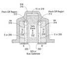
- FIG. 3Ashows a cross-sectional view of the FinFET device formed by either the exemplary process of FIG. 1 or the exemplary process of FIG. 2 .
- the gate stack 6 or 102is shown disposed between the SiN spacers 8 or 106 , respectively.
- Source (S) and drain (D) implants 300 , 302may be located in the underlying SOI or bulk substrate material.
- FIG. 3Bshows a result of further processing in accordance with embodiments of this invention, wherein the SiN spacers 8 or 106 are removed. This can be accomplished by a wet chemical etch process, such as by the use of hot phosphoric acid.
- FIG. 3Cshows a result of the deposition of an interlayer dielectric (ILD) layer, such as a SiN capping layer 310 .
- ILDinterlayer dielectric
- the SiN capping layer 310substantially uniformly coats the structure of the FinFET 20 or 100 .
- a pinch-off region 312is formed near to the top leaving an underlying air gap 314 disposed adjacent to sidewalls of the gate stack 6 or 102 .
- the air gap 314is substantially continuous along the sidewalls of the gate stack except for where the fin 5 or 205 extends from the silicided portions 10 or 216 into the gate stack 6 or 102 .
- the thickness of the original SiN spacers 8 or 106can be in a range of about 5 nm to about 10 nm, which then becomes the approximate width of the air gap 314 .
- the SiN capping layercan be deposited using a relatively low temperature (e.g., approximately 350° C.) plasma-enhanced chemical vapor deposition (PECVD) process. Si 3 N 4 using the low temperature ( ⁇ 350° C.) PECVD process is a non-limiting example of one suitable process to form the capping layer to create the airgap 314 .
- PECVDplasma-enhanced chemical vapor deposition
- the dielectric constant of airis about unity as compared to the dielectric constant of SiN which is about 7-7.5.
- the resulting spacer formed by the air gap 314thus provides enhanced electrical performance by reducing parasitic capacitance between the gate and the source/drains, i.e., between the gate stack 6 or 102 and the fins 5 or 205 of the exemplary FinFET embodiments 20 or 100 of FIGS. 1 and 2 , respectively.
- the FinFET 20 or 100 in accordance with the exemplary embodiments of this inventioncan be implemented as an N-type device or a P-type device.
- the gate stackscan be fabricated using poly Si or metal, any suitable gate dielectric material can be used, and the silicide layers can be composed of any suitable type of silicide.
- the FinFETs 20 or 100can be constructed to have single fin or channel structure passing through the width of the gate stack, or there can be two or more fins or channel structures passing through the width of the gate stack.
- the exemplary embodiments of this inventionapply to multi-gate transistors.
- the exemplary embodiments of this inventionalso apply to wire-type transistors, wherein the channel structure passes through the width of the gate stack such that all surfaces of the channel structure (i.e., top surface, two side surfaces, and the bottom surface) are adjacent to or surrounded by the gate stack and can be electrically influenced by the gate stack.
Landscapes
- Thin Film Transistor (AREA)
- Insulated Gate Type Field-Effect Transistor (AREA)
Abstract
Description
Claims (14)
Priority Applications (5)
| Application Number | Priority Date | Filing Date | Title |
|---|---|---|---|
| US13/272,409US8637930B2 (en) | 2011-10-13 | 2011-10-13 | FinFET parasitic capacitance reduction using air gap |
| US13/617,426US8637384B2 (en) | 2011-10-13 | 2012-09-14 | FinFET parasitic capacitance reduction using air gap |
| DE102012217491.5ADE102012217491B4 (en) | 2011-10-13 | 2012-09-26 | TRANSISTOR, METHOD FOR MANUFACTURING A TRANSISTOR AND METHOD FOR REDUCING THE PARASITIC CAPACITY IN A MULTI-GATE FIELD-EFFECT TRANSISTOR |
| GB1217771.3AGB2495606B (en) | 2011-10-13 | 2012-10-04 | FinFET parasitic capacitance reduction using air gap |
| CN201210385506.XACN103050515B (en) | 2011-10-13 | 2012-10-12 | Transistor and manufacture method thereof |
Applications Claiming Priority (1)
| Application Number | Priority Date | Filing Date | Title |
|---|---|---|---|
| US13/272,409US8637930B2 (en) | 2011-10-13 | 2011-10-13 | FinFET parasitic capacitance reduction using air gap |
Related Child Applications (1)
| Application Number | Title | Priority Date | Filing Date |
|---|---|---|---|
| US13/617,426ContinuationUS8637384B2 (en) | 2011-10-13 | 2012-09-14 | FinFET parasitic capacitance reduction using air gap |
Publications (2)
| Publication Number | Publication Date |
|---|---|
| US20130093019A1 US20130093019A1 (en) | 2013-04-18 |
| US8637930B2true US8637930B2 (en) | 2014-01-28 |
Family
ID=47225676
Family Applications (2)
| Application Number | Title | Priority Date | Filing Date |
|---|---|---|---|
| US13/272,409Active2032-01-25US8637930B2 (en) | 2011-10-13 | 2011-10-13 | FinFET parasitic capacitance reduction using air gap |
| US13/617,426ActiveUS8637384B2 (en) | 2011-10-13 | 2012-09-14 | FinFET parasitic capacitance reduction using air gap |
Family Applications After (1)
| Application Number | Title | Priority Date | Filing Date |
|---|---|---|---|
| US13/617,426ActiveUS8637384B2 (en) | 2011-10-13 | 2012-09-14 | FinFET parasitic capacitance reduction using air gap |
Country Status (4)
| Country | Link |
|---|---|
| US (2) | US8637930B2 (en) |
| CN (1) | CN103050515B (en) |
| DE (1) | DE102012217491B4 (en) |
| GB (1) | GB2495606B (en) |
Cited By (38)
| Publication number | Priority date | Publication date | Assignee | Title |
|---|---|---|---|---|
| US20140203348A1 (en)* | 2013-01-23 | 2014-07-24 | Samsung Electronics Co., Ltd. | Semiconductor devices and methods of fabricating the same |
| US8826213B1 (en)* | 2013-03-11 | 2014-09-02 | Taiwan Semiconductor Manufacturing Company, Ltd. | Parasitic capacitance extraction for FinFETs |
| US20150076693A1 (en)* | 2011-10-12 | 2015-03-19 | SK Hynix Inc. | Semiconductor device with damascene bit line and method for fabricating the same |
| US9299835B1 (en) | 2014-12-04 | 2016-03-29 | International Business Machines Corporation | Vertical field effect transistors |
| US9362355B1 (en) | 2015-11-13 | 2016-06-07 | International Business Machines Corporation | Nanosheet MOSFET with full-height air-gap spacer |
| US9368572B1 (en) | 2015-11-21 | 2016-06-14 | International Business Machines Corporation | Vertical transistor with air-gap spacer |
| US9419091B1 (en)* | 2015-02-04 | 2016-08-16 | International Business Machines Corporation | Trenched gate with sidewall airgap spacer |
| US9443982B1 (en) | 2016-02-08 | 2016-09-13 | International Business Machines Corporation | Vertical transistor with air gap spacers |
| US20160372382A1 (en)* | 2015-06-16 | 2016-12-22 | Samsung Electronics Co., Ltd. | Semiconductor device and method of fabricating the same |
| US9608065B1 (en) | 2016-06-03 | 2017-03-28 | International Business Machines Corporation | Air gap spacer for metal gates |
| US9673293B1 (en) | 2016-02-18 | 2017-06-06 | International Business Machines Corporation | Airgap spacers |
| US20170162650A1 (en)* | 2015-12-03 | 2017-06-08 | International Business Machines Corporation | Finfet with reduced parasitic capacitance |
| US9735246B1 (en) | 2016-05-11 | 2017-08-15 | International Business Machines Corporation | Air-gap top spacer and self-aligned metal gate for vertical fets |
| US9773881B2 (en)* | 2015-11-03 | 2017-09-26 | International Business Machines Corporation | Etch stop for airgap protection |
| US9805935B2 (en)* | 2015-12-31 | 2017-10-31 | International Business Machines Corporation | Bottom source/drain silicidation for vertical field-effect transistor (FET) |
| US9865738B2 (en)* | 2016-04-29 | 2018-01-09 | Samsung Electronics Co., Ltd. | Fin field effect transistor (FinFET) having air gap and method of fabricating the same |
| US9892961B1 (en) | 2016-08-09 | 2018-02-13 | International Business Machines Corporation | Air gap spacer formation for nano-scale semiconductor devices |
| US9941352B1 (en) | 2016-10-05 | 2018-04-10 | International Business Machines Corporation | Transistor with improved air spacer |
| US20180138279A1 (en)* | 2016-11-15 | 2018-05-17 | Globalfoundries Inc. | Transistor-based semiconductor device with air-gap spacers and gate contact over active area |
| US10199503B2 (en) | 2017-04-24 | 2019-02-05 | International Business Machines Corporation | Under-channel gate transistors |
| US10229986B1 (en) | 2017-12-04 | 2019-03-12 | International Business Machines Corporation | Vertical transport field-effect transistor including dual layer top spacer |
| US10256296B2 (en) | 2015-11-24 | 2019-04-09 | International Business Machines Corporation | Middle-of-line (MOL) capacitance reduction for self-aligned contact in gate stack |
| TWI657538B (en)* | 2016-12-13 | 2019-04-21 | 美商格芯(美國)集成電路科技有限公司 | Air-gap spacers for field-effect transistors |
| US10319833B1 (en)* | 2017-12-04 | 2019-06-11 | International Business Machines Corporation | Vertical transport field-effect transistor including air-gap top spacer |
| US10388747B1 (en) | 2018-03-28 | 2019-08-20 | Globalfoundries Inc. | Gate contact structure positioned above an active region with air gaps positioned adjacent the gate structure |
| US10411107B2 (en) | 2017-09-01 | 2019-09-10 | Globalfoundries Inc. | Semiconductor device with airgap spacer for transistor and related method |
| US10411114B2 (en) | 2017-12-21 | 2019-09-10 | International Business Machines Corporation | Air gap spacer with wrap-around etch stop layer under gate spacer |
| US10535771B1 (en) | 2018-06-25 | 2020-01-14 | Globalfoundries Inc. | Method for forming replacement air gap |
| US10535652B2 (en) | 2016-10-27 | 2020-01-14 | International Business Machines Corporation | Fabrication of vertical fin field effect transistors having top air spacers and a self-aligned top junction |
| US10680102B2 (en) | 2018-09-27 | 2020-06-09 | International Business Machines Corporation | Reduction of top source/drain external resistance and parasitic capacitance in vertical transistors |
| US10692987B2 (en)* | 2018-10-19 | 2020-06-23 | Globalfoundries Inc. | IC structure with air gap adjacent to gate structure and methods of forming same |
| US10886378B2 (en) | 2019-01-02 | 2021-01-05 | Globalfoundries Inc. | Method of forming air-gap spacers and gate contact over active region and the resulting device |
| US10903331B2 (en) | 2019-03-25 | 2021-01-26 | International Business Machines Corporation | Positioning air-gap spacers in a transistor for improved control of parasitic capacitance |
| US11094796B2 (en) | 2019-09-30 | 2021-08-17 | Taiwan Semiconductor Manufacturing Co., Ltd. | Transistor spacer structures |
| US11145540B2 (en)* | 2019-08-08 | 2021-10-12 | Nanya Technology Corporation | Semiconductor structure having air gap dielectric and the method of preparing the same |
| US11393717B2 (en)* | 2018-10-23 | 2022-07-19 | Taiwan Semiconductor Manufacturing Co., Ltd. | Insulating cap on contact structure and method for forming the same |
| US11417750B2 (en) | 2020-01-31 | 2022-08-16 | Taiwan Semiconductor Manufacturing Co., Ltd. | Gate air spacer for fin-like field effect transistor |
| US12211922B2 (en) | 2020-01-31 | 2025-01-28 | Taiwan Semiconductor Manufacturing Co., Ltd. | Gate air spacer for fin-like field effect transistor |
Families Citing this family (303)
| Publication number | Priority date | Publication date | Assignee | Title |
|---|---|---|---|---|
| US20130023129A1 (en) | 2011-07-20 | 2013-01-24 | Asm America, Inc. | Pressure transmitter for a semiconductor processing environment |
| US8871626B2 (en)* | 2011-12-20 | 2014-10-28 | International Business Machines Corporation | FinFET with vertical silicide structure |
| US20140201151A1 (en) | 2013-01-11 | 2014-07-17 | Commvault Systems, Inc. | Systems and methods to select files for restoration from block-level backup for virtual machines |
| US20160376700A1 (en) | 2013-02-01 | 2016-12-29 | Asm Ip Holding B.V. | System for treatment of deposition reactor |
| US9040363B2 (en) | 2013-03-20 | 2015-05-26 | International Business Machines Corporation | FinFET with reduced capacitance |
| CN104167393B (en)* | 2013-05-17 | 2018-09-18 | 中国科学院微电子研究所 | Semiconductor device manufacturing method |
| US9023697B2 (en)* | 2013-08-08 | 2015-05-05 | International Business Machines Corporation | 3D transistor channel mobility enhancement |
| CN104425594B (en)* | 2013-08-20 | 2018-07-10 | 中芯国际集成电路制造(上海)有限公司 | Fin formula field effect transistor and forming method thereof |
| US9391202B2 (en) | 2013-09-24 | 2016-07-12 | Samsung Electronics Co., Ltd. | Semiconductor device |
| KR102200928B1 (en) | 2014-02-18 | 2021-01-11 | 삼성전자주식회사 | Transistor having ultra low parasitic capacitance component and method for manufacturing the same |
| US9543407B2 (en)* | 2014-02-27 | 2017-01-10 | International Business Machines Corporation | Low-K spacer for RMG finFET formation |
| US9871121B2 (en) | 2014-03-10 | 2018-01-16 | Qualcomm Incorporated | Semiconductor device having a gap defined therein |
| US9318574B2 (en)* | 2014-06-18 | 2016-04-19 | International Business Machines Corporation | Method and structure for enabling high aspect ratio sacrificial gates |
| US9293523B2 (en) | 2014-06-24 | 2016-03-22 | Applied Materials, Inc. | Method of forming III-V channel |
| US9349649B2 (en) | 2014-06-26 | 2016-05-24 | Globalfoundries Inc. | Low resistance and defect free epitaxial semiconductor material for providing merged FinFETs |
| KR102235614B1 (en) | 2014-09-17 | 2021-04-02 | 삼성전자주식회사 | Integrated circuit device and method of manufacturing the same |
| US10941490B2 (en) | 2014-10-07 | 2021-03-09 | Asm Ip Holding B.V. | Multiple temperature range susceptor, assembly, reactor and system including the susceptor, and methods of using the same |
| US9484250B2 (en) | 2015-03-10 | 2016-11-01 | International Business Machines Corporation | Air gap contact formation for reducing parasitic capacitance |
| US10276355B2 (en) | 2015-03-12 | 2019-04-30 | Asm Ip Holding B.V. | Multi-zone reactor, system including the reactor, and method of using the same |
| KR102365305B1 (en) | 2015-03-27 | 2022-02-22 | 삼성전자주식회사 | Semiconductor device |
| WO2017014725A1 (en)* | 2015-07-17 | 2017-01-26 | Intel Corporation | Transistor with airgap spacer |
| US9666581B2 (en) | 2015-08-21 | 2017-05-30 | Taiwan Semiconductor Manufacturing Company, Ltd. | FinFET with source/drain structure and method of fabrication thereof |
| US9911824B2 (en) | 2015-09-18 | 2018-03-06 | Taiwan Semiconductor Manufacturing Co., Ltd. | Semiconductor structure with multi spacer |
| US10622457B2 (en) | 2015-10-09 | 2020-04-14 | International Business Machines Corporation | Forming replacement low-K spacer in tight pitch fin field effect transistors |
| US10181527B2 (en) | 2015-10-16 | 2019-01-15 | Samsung Electronics Co., Ltd. | FinFet having dual vertical spacer and method of manufacturing the same |
| US9530890B1 (en) | 2015-11-02 | 2016-12-27 | International Business Machines Corporation | Parasitic capacitance reduction |
| US9716154B2 (en) | 2015-12-17 | 2017-07-25 | Taiwan Semiconductor Manufacturing Co., Ltd. | Semiconductor structure having a gas-filled gap |
| US10164029B2 (en) | 2015-12-18 | 2018-12-25 | Taiwan Semiconductor Manufacturing Company, Ltd. | Semiconductor structure and manufacturing method thereof |
| US11139308B2 (en) | 2015-12-29 | 2021-10-05 | Asm Ip Holding B.V. | Atomic layer deposition of III-V compounds to form V-NAND devices |
| TWI663729B (en)* | 2016-01-05 | 2019-06-21 | 聯華電子股份有限公司 | Semiconductor structure and method for manufacturing the same |
| US10388564B2 (en) | 2016-01-12 | 2019-08-20 | Micron Technology, Inc. | Method for fabricating a memory device having two contacts |
| US9935199B2 (en) | 2016-01-15 | 2018-04-03 | Taiwan Semiconductor Manufacturing Company, Ltd. | FinFET with source/drain structure |
| US10224235B2 (en)* | 2016-02-05 | 2019-03-05 | Lam Research Corporation | Systems and methods for creating airgap seals using atomic layer deposition and high density plasma chemical vapor deposition |
| US10529554B2 (en) | 2016-02-19 | 2020-01-07 | Asm Ip Holding B.V. | Method for forming silicon nitride film selectively on sidewalls or flat surfaces of trenches |
| WO2017151148A1 (en)* | 2016-03-04 | 2017-09-08 | Intel Corporation | Field effect transistors with a gated oxide semiconductor source/drain spacer |
| US10343920B2 (en) | 2016-03-18 | 2019-07-09 | Asm Ip Holding B.V. | Aligned carbon nanotubes |
| US9716158B1 (en)* | 2016-03-21 | 2017-07-25 | International Business Machines Corporation | Air gap spacer between contact and gate region |
| CN116110941A (en) | 2016-04-25 | 2023-05-12 | 应用材料公司 | Forming horizontal surrounding gate element nanowire air gap spacing |
| US11453943B2 (en) | 2016-05-25 | 2022-09-27 | Asm Ip Holding B.V. | Method for forming carbon-containing silicon/metal oxide or nitride film by ALD using silicon precursor and hydrocarbon precursor |
| US9748380B1 (en) | 2016-06-29 | 2017-08-29 | International Business Machines Corporation | Vertical transistor including a bottom source/drain region, a gate structure, and an air gap formed between the bottom source/drain region and the gate structure |
| US9859151B1 (en) | 2016-07-08 | 2018-01-02 | Asm Ip Holding B.V. | Selective film deposition method to form air gaps |
| US10612137B2 (en) | 2016-07-08 | 2020-04-07 | Asm Ip Holdings B.V. | Organic reactants for atomic layer deposition |
| US9812320B1 (en) | 2016-07-28 | 2017-11-07 | Asm Ip Holding B.V. | Method and apparatus for filling a gap |
| US9887082B1 (en) | 2016-07-28 | 2018-02-06 | Asm Ip Holding B.V. | Method and apparatus for filling a gap |
| US9911804B1 (en) | 2016-08-22 | 2018-03-06 | International Business Machines Corporation | Vertical fin field effect transistor with air gap spacers |
| US9721897B1 (en) | 2016-09-27 | 2017-08-01 | International Business Machines Corporation | Transistor with air spacer and self-aligned contact |
| US9985109B2 (en) | 2016-10-25 | 2018-05-29 | International Business Machines Corporation | FinFET with reduced parasitic capacitance |
| US11532757B2 (en) | 2016-10-27 | 2022-12-20 | Asm Ip Holding B.V. | Deposition of charge trapping layers |
| US9960275B1 (en) | 2016-10-28 | 2018-05-01 | Applied Materials, Inc. | Method of fabricating air-gap spacer for N7/N5 finFET and beyond |
| US10714350B2 (en) | 2016-11-01 | 2020-07-14 | ASM IP Holdings, B.V. | Methods for forming a transition metal niobium nitride film on a substrate by atomic layer deposition and related semiconductor device structures |
| KR102546317B1 (en) | 2016-11-15 | 2023-06-21 | 에이에스엠 아이피 홀딩 비.브이. | Gas supply unit and substrate processing apparatus including the same |
| CN108122973B (en) | 2016-11-28 | 2020-06-09 | 中芯国际集成电路制造(上海)有限公司 | Semiconductor structure, forming method thereof and SRAM |
| US11447861B2 (en) | 2016-12-15 | 2022-09-20 | Asm Ip Holding B.V. | Sequential infiltration synthesis apparatus and a method of forming a patterned structure |
| US11581186B2 (en) | 2016-12-15 | 2023-02-14 | Asm Ip Holding B.V. | Sequential infiltration synthesis apparatus |
| US11390950B2 (en) | 2017-01-10 | 2022-07-19 | Asm Ip Holding B.V. | Reactor system and method to reduce residue buildup during a film deposition process |
| US10468261B2 (en) | 2017-02-15 | 2019-11-05 | Asm Ip Holding B.V. | Methods for forming a metallic film on a substrate by cyclical deposition and related semiconductor device structures |
| US10211100B2 (en)* | 2017-03-27 | 2019-02-19 | Globalfoundries Inc. | Methods of forming an air gap adjacent a gate of a transistor and a gate contact above the active region of the transistor |
| US10770286B2 (en) | 2017-05-08 | 2020-09-08 | Asm Ip Holdings B.V. | Methods for selectively forming a silicon nitride film on a substrate and related semiconductor device structures |
| EP3404702A1 (en)* | 2017-05-15 | 2018-11-21 | IMEC vzw | A method for forming vertical channel devices |
| US12040200B2 (en) | 2017-06-20 | 2024-07-16 | Asm Ip Holding B.V. | Semiconductor processing apparatus and methods for calibrating a semiconductor processing apparatus |
| US11306395B2 (en) | 2017-06-28 | 2022-04-19 | Asm Ip Holding B.V. | Methods for depositing a transition metal nitride film on a substrate by atomic layer deposition and related deposition apparatus |
| CN109216357B (en)* | 2017-06-30 | 2021-04-20 | 联华电子股份有限公司 | Semiconductor structure and method of making the same |
| KR20190009245A (en) | 2017-07-18 | 2019-01-28 | 에이에스엠 아이피 홀딩 비.브이. | Methods for forming a semiconductor device structure and related semiconductor device structures |
| US11374112B2 (en) | 2017-07-19 | 2022-06-28 | Asm Ip Holding B.V. | Method for depositing a group IV semiconductor and related semiconductor device structures |
| US10590535B2 (en) | 2017-07-26 | 2020-03-17 | Asm Ip Holdings B.V. | Chemical treatment, deposition and/or infiltration apparatus and method for using the same |
| TWI815813B (en) | 2017-08-04 | 2023-09-21 | 荷蘭商Asm智慧財產控股公司 | Showerhead assembly for distributing a gas within a reaction chamber |
| US10692741B2 (en) | 2017-08-08 | 2020-06-23 | Asm Ip Holdings B.V. | Radiation shield |
| US10770336B2 (en) | 2017-08-08 | 2020-09-08 | Asm Ip Holding B.V. | Substrate lift mechanism and reactor including same |
| US11769682B2 (en) | 2017-08-09 | 2023-09-26 | Asm Ip Holding B.V. | Storage apparatus for storing cassettes for substrates and processing apparatus equipped therewith |
| US10510860B2 (en)* | 2017-08-29 | 2019-12-17 | Taiwan Semiconductor Manufacturing Co., Ltd. | Semiconductor device and method of manufacturing the same |
| US11830730B2 (en) | 2017-08-29 | 2023-11-28 | Asm Ip Holding B.V. | Layer forming method and apparatus |
| DE102017126049B4 (en)* | 2017-08-29 | 2024-01-25 | Taiwan Semiconductor Manufacturing Co., Ltd. | METHOD FOR PRODUCING A SEMICONDUCTOR DEVICE |
| US11295980B2 (en) | 2017-08-30 | 2022-04-05 | Asm Ip Holding B.V. | Methods for depositing a molybdenum metal film over a dielectric surface of a substrate by a cyclical deposition process and related semiconductor device structures |
| US10658205B2 (en) | 2017-09-28 | 2020-05-19 | Asm Ip Holdings B.V. | Chemical dispensing apparatus and methods for dispensing a chemical to a reaction chamber |
| US10483372B2 (en)* | 2017-09-29 | 2019-11-19 | Taiwan Semiconductor Manufacturing Co., Ltd. | Spacer structure with high plasma resistance for semiconductor devices |
| CN109599337A (en)* | 2017-09-30 | 2019-04-09 | 中芯国际集成电路制造(上海)有限公司 | Semiconductor devices and forming method thereof |
| US10403504B2 (en) | 2017-10-05 | 2019-09-03 | Asm Ip Holding B.V. | Method for selectively depositing a metallic film on a substrate |
| US10923344B2 (en) | 2017-10-30 | 2021-02-16 | Asm Ip Holding B.V. | Methods for forming a semiconductor structure and related semiconductor structures |
| CN111344522B (en) | 2017-11-27 | 2022-04-12 | 阿斯莫Ip控股公司 | Including clean mini-environment device |
| WO2019103613A1 (en) | 2017-11-27 | 2019-05-31 | Asm Ip Holding B.V. | A storage device for storing wafer cassettes for use with a batch furnace |
| US10347744B1 (en) | 2018-01-09 | 2019-07-09 | International Business Machines Corporation | Method and structure of forming FinFET contact |
| US10872771B2 (en) | 2018-01-16 | 2020-12-22 | Asm Ip Holding B. V. | Method for depositing a material film on a substrate within a reaction chamber by a cyclical deposition process and related device structures |
| TWI799494B (en) | 2018-01-19 | 2023-04-21 | 荷蘭商Asm 智慧財產控股公司 | Deposition method |
| KR102695659B1 (en) | 2018-01-19 | 2024-08-14 | 에이에스엠 아이피 홀딩 비.브이. | Method for depositing a gap filling layer by plasma assisted deposition |
| US10367076B1 (en) | 2018-01-31 | 2019-07-30 | International Business Machines Corporation | Air gap spacer with controlled air gap height |
| US11081345B2 (en) | 2018-02-06 | 2021-08-03 | Asm Ip Holding B.V. | Method of post-deposition treatment for silicon oxide film |
| US10896820B2 (en) | 2018-02-14 | 2021-01-19 | Asm Ip Holding B.V. | Method for depositing a ruthenium-containing film on a substrate by a cyclical deposition process |
| WO2019158960A1 (en) | 2018-02-14 | 2019-08-22 | Asm Ip Holding B.V. | A method for depositing a ruthenium-containing film on a substrate by a cyclical deposition process |
| US10731249B2 (en) | 2018-02-15 | 2020-08-04 | Asm Ip Holding B.V. | Method of forming a transition metal containing film on a substrate by a cyclical deposition process, a method for supplying a transition metal halide compound to a reaction chamber, and related vapor deposition apparatus |
| KR102636427B1 (en) | 2018-02-20 | 2024-02-13 | 에이에스엠 아이피 홀딩 비.브이. | Substrate processing method and apparatus |
| US10975470B2 (en) | 2018-02-23 | 2021-04-13 | Asm Ip Holding B.V. | Apparatus for detecting or monitoring for a chemical precursor in a high temperature environment |
| US11473195B2 (en) | 2018-03-01 | 2022-10-18 | Asm Ip Holding B.V. | Semiconductor processing apparatus and a method for processing a substrate |
| KR102646467B1 (en) | 2018-03-27 | 2024-03-11 | 에이에스엠 아이피 홀딩 비.브이. | Method of forming an electrode on a substrate and a semiconductor device structure including an electrode |
| KR102600229B1 (en) | 2018-04-09 | 2023-11-10 | 에이에스엠 아이피 홀딩 비.브이. | Substrate supporting device, substrate processing apparatus including the same and substrate processing method |
| CN110400751B (en)* | 2018-04-25 | 2024-04-26 | 中芯国际集成电路制造(上海)有限公司 | Semiconductor device, manufacturing method thereof and electronic device |
| US10522649B2 (en) | 2018-04-27 | 2019-12-31 | International Business Machines Corporation | Inverse T-shaped contact structures having air gap spacers |
| US10861953B2 (en) | 2018-04-30 | 2020-12-08 | Taiwan Semiconductor Manufacturing Company, Ltd. | Air spacers in transistors and methods forming same |
| US10833165B2 (en) | 2018-04-30 | 2020-11-10 | International Business Machines Corporation | Asymmetric air spacer gate-controlled device with reduced parasitic capacitance |
| US12025484B2 (en) | 2018-05-08 | 2024-07-02 | Asm Ip Holding B.V. | Thin film forming method |
| US12272527B2 (en) | 2018-05-09 | 2025-04-08 | Asm Ip Holding B.V. | Apparatus for use with hydrogen radicals and method of using same |
| KR102596988B1 (en) | 2018-05-28 | 2023-10-31 | 에이에스엠 아이피 홀딩 비.브이. | Method of processing a substrate and a device manufactured by the same |
| US11718913B2 (en) | 2018-06-04 | 2023-08-08 | Asm Ip Holding B.V. | Gas distribution system and reactor system including same |
| US10608096B2 (en) | 2018-06-11 | 2020-03-31 | International Business Machines Corporation | Formation of air gap spacers for reducing parasitic capacitance |
| US10797133B2 (en) | 2018-06-21 | 2020-10-06 | Asm Ip Holding B.V. | Method for depositing a phosphorus doped silicon arsenide film and related semiconductor device structures |
| KR102568797B1 (en) | 2018-06-21 | 2023-08-21 | 에이에스엠 아이피 홀딩 비.브이. | Substrate processing system |
| TWI873894B (en) | 2018-06-27 | 2025-02-21 | 荷蘭商Asm Ip私人控股有限公司 | Cyclic deposition methods for forming metal-containing material and films and structures including the metal-containing material |
| KR102854019B1 (en) | 2018-06-27 | 2025-09-02 | 에이에스엠 아이피 홀딩 비.브이. | Periodic deposition method for forming a metal-containing material and films and structures comprising the metal-containing material |
| US10388513B1 (en) | 2018-07-03 | 2019-08-20 | Asm Ip Holding B.V. | Method for depositing silicon-free carbon-containing film as gap-fill layer by pulse plasma-assisted deposition |
| US10755922B2 (en) | 2018-07-03 | 2020-08-25 | Asm Ip Holding B.V. | Method for depositing silicon-free carbon-containing film as gap-fill layer by pulse plasma-assisted deposition |
| US10854503B2 (en)* | 2018-07-16 | 2020-12-01 | Taiwan Semiconductor Manufacturing Co., Ltd. | Semiconductor structure with air gap and method sealing the air gap |
| US11430674B2 (en) | 2018-08-22 | 2022-08-30 | Asm Ip Holding B.V. | Sensor array, apparatus for dispensing a vapor phase reactant to a reaction chamber and related methods |
| US10950692B2 (en)* | 2018-09-04 | 2021-03-16 | Globalfoundries U.S. Inc. | Methods of forming air gaps between source/drain contacts and the resulting devices |
| US11024523B2 (en) | 2018-09-11 | 2021-06-01 | Asm Ip Holding B.V. | Substrate processing apparatus and method |
| KR102707956B1 (en) | 2018-09-11 | 2024-09-19 | 에이에스엠 아이피 홀딩 비.브이. | Method for deposition of a thin film |
| US10580692B1 (en) | 2018-09-12 | 2020-03-03 | International Business Machines Corporation | Integration of air spacer with self-aligned contact in transistor |
| CN110970344B (en) | 2018-10-01 | 2024-10-25 | Asmip控股有限公司 | Substrate holding apparatus, system comprising the same and method of using the same |
| KR102592699B1 (en) | 2018-10-08 | 2023-10-23 | 에이에스엠 아이피 홀딩 비.브이. | Substrate support unit and apparatuses for depositing thin film and processing the substrate including the same |
| KR102546322B1 (en) | 2018-10-19 | 2023-06-21 | 에이에스엠 아이피 홀딩 비.브이. | Substrate processing apparatus and substrate processing method |
| US12378665B2 (en) | 2018-10-26 | 2025-08-05 | Asm Ip Holding B.V. | High temperature coatings for a preclean and etch apparatus and related methods |
| US11087997B2 (en) | 2018-10-31 | 2021-08-10 | Asm Ip Holding B.V. | Substrate processing apparatus for processing substrates |
| KR102748291B1 (en) | 2018-11-02 | 2024-12-31 | 에이에스엠 아이피 홀딩 비.브이. | Substrate support unit and substrate processing apparatus including the same |
| US11572620B2 (en) | 2018-11-06 | 2023-02-07 | Asm Ip Holding B.V. | Methods for selectively depositing an amorphous silicon film on a substrate |
| US10818758B2 (en) | 2018-11-16 | 2020-10-27 | Asm Ip Holding B.V. | Methods for forming a metal silicate film on a substrate in a reaction chamber and related semiconductor device structures |
| US12040199B2 (en) | 2018-11-28 | 2024-07-16 | Asm Ip Holding B.V. | Substrate processing apparatus for processing substrates |
| KR102636428B1 (en) | 2018-12-04 | 2024-02-13 | 에이에스엠 아이피 홀딩 비.브이. | A method for cleaning a substrate processing apparatus |
| US11158513B2 (en) | 2018-12-13 | 2021-10-26 | Asm Ip Holding B.V. | Methods for forming a rhenium-containing film on a substrate by a cyclical deposition process and related semiconductor device structures |
| TWI874340B (en) | 2018-12-14 | 2025-03-01 | 荷蘭商Asm Ip私人控股有限公司 | Method of forming device structure, structure formed by the method and system for performing the method |
| US10840351B2 (en)* | 2019-01-03 | 2020-11-17 | International Business Machines Corporation | Transistor with airgap spacer and tight gate pitch |
| TWI866480B (en) | 2019-01-17 | 2024-12-11 | 荷蘭商Asm Ip 私人控股有限公司 | Methods of forming a transition metal containing film on a substrate by a cyclical deposition process |
| TWI873122B (en) | 2019-02-20 | 2025-02-21 | 荷蘭商Asm Ip私人控股有限公司 | Method of filling a recess formed within a surface of a substrate, semiconductor structure formed according to the method, and semiconductor processing apparatus |
| TWI845607B (en) | 2019-02-20 | 2024-06-21 | 荷蘭商Asm Ip私人控股有限公司 | Cyclical deposition method and apparatus for filling a recess formed within a substrate surface |
| TWI838458B (en) | 2019-02-20 | 2024-04-11 | 荷蘭商Asm Ip私人控股有限公司 | Apparatus and methods for plug fill deposition in 3-d nand applications |
| TWI842826B (en) | 2019-02-22 | 2024-05-21 | 荷蘭商Asm Ip私人控股有限公司 | Substrate processing apparatus and method for processing substrate |
| KR102858005B1 (en) | 2019-03-08 | 2025-09-09 | 에이에스엠 아이피 홀딩 비.브이. | Method for Selective Deposition of Silicon Nitride Layer and Structure Including Selectively-Deposited Silicon Nitride Layer |
| US11742198B2 (en) | 2019-03-08 | 2023-08-29 | Asm Ip Holding B.V. | Structure including SiOCN layer and method of forming same |
| US11798838B2 (en)* | 2019-03-19 | 2023-10-24 | Intel Corporation | Capacitance reduction for semiconductor devices based on wafer bonding |
| JP2020167398A (en) | 2019-03-28 | 2020-10-08 | エーエスエム・アイピー・ホールディング・ベー・フェー | Door openers and substrate processing equipment provided with door openers |
| KR102809999B1 (en) | 2019-04-01 | 2025-05-19 | 에이에스엠 아이피 홀딩 비.브이. | Method of manufacturing semiconductor device |
| KR20200123380A (en) | 2019-04-19 | 2020-10-29 | 에이에스엠 아이피 홀딩 비.브이. | Layer forming method and apparatus |
| KR20200125453A (en) | 2019-04-24 | 2020-11-04 | 에이에스엠 아이피 홀딩 비.브이. | Gas-phase reactor system and method of using same |
| KR20200130121A (en) | 2019-05-07 | 2020-11-18 | 에이에스엠 아이피 홀딩 비.브이. | Chemical source vessel with dip tube |
| KR20200130652A (en) | 2019-05-10 | 2020-11-19 | 에이에스엠 아이피 홀딩 비.브이. | Method of depositing material onto a surface and structure formed according to the method |
| JP7598201B2 (en) | 2019-05-16 | 2024-12-11 | エーエスエム・アイピー・ホールディング・ベー・フェー | Wafer boat handling apparatus, vertical batch furnace and method |
| JP7612342B2 (en) | 2019-05-16 | 2025-01-14 | エーエスエム・アイピー・ホールディング・ベー・フェー | Wafer boat handling apparatus, vertical batch furnace and method |
| USD947913S1 (en) | 2019-05-17 | 2022-04-05 | Asm Ip Holding B.V. | Susceptor shaft |
| USD975665S1 (en) | 2019-05-17 | 2023-01-17 | Asm Ip Holding B.V. | Susceptor shaft |
| KR20200141002A (en) | 2019-06-06 | 2020-12-17 | 에이에스엠 아이피 홀딩 비.브이. | Method of using a gas-phase reactor system including analyzing exhausted gas |
| KR20200141931A (en) | 2019-06-10 | 2020-12-21 | 에이에스엠 아이피 홀딩 비.브이. | Method for cleaning quartz epitaxial chambers |
| KR20200143254A (en) | 2019-06-11 | 2020-12-23 | 에이에스엠 아이피 홀딩 비.브이. | Method of forming an electronic structure using an reforming gas, system for performing the method, and structure formed using the method |
| KR20210005515A (en) | 2019-07-03 | 2021-01-14 | 에이에스엠 아이피 홀딩 비.브이. | Temperature control assembly for substrate processing apparatus and method of using same |
| US10978574B2 (en) | 2019-07-08 | 2021-04-13 | International Business Machines Corporation | Floating gate prevention and capacitance reduction in semiconductor devices |
| JP7499079B2 (en) | 2019-07-09 | 2024-06-13 | エーエスエム・アイピー・ホールディング・ベー・フェー | Plasma device using coaxial waveguide and substrate processing method |
| CN112216646A (en) | 2019-07-10 | 2021-01-12 | Asm Ip私人控股有限公司 | Substrate supporting assembly and substrate processing device comprising same |
| KR20210010307A (en) | 2019-07-16 | 2021-01-27 | 에이에스엠 아이피 홀딩 비.브이. | Substrate processing apparatus |
| KR20210010816A (en) | 2019-07-17 | 2021-01-28 | 에이에스엠 아이피 홀딩 비.브이. | Radical assist ignition plasma system and method |
| KR102860110B1 (en) | 2019-07-17 | 2025-09-16 | 에이에스엠 아이피 홀딩 비.브이. | Methods of forming silicon germanium structures |
| US11643724B2 (en) | 2019-07-18 | 2023-05-09 | Asm Ip Holding B.V. | Method of forming structures using a neutral beam |
| KR20210010817A (en) | 2019-07-19 | 2021-01-28 | 에이에스엠 아이피 홀딩 비.브이. | Method of Forming Topology-Controlled Amorphous Carbon Polymer Film |
| TWI851767B (en) | 2019-07-29 | 2024-08-11 | 荷蘭商Asm Ip私人控股有限公司 | Methods for selective deposition utilizing n-type dopants and/or alternative dopants to achieve high dopant incorporation |
| CN112309900A (en) | 2019-07-30 | 2021-02-02 | Asm Ip私人控股有限公司 | Substrate processing apparatus |
| US12169361B2 (en) | 2019-07-30 | 2024-12-17 | Asm Ip Holding B.V. | Substrate processing apparatus and method |
| CN112309899A (en) | 2019-07-30 | 2021-02-02 | Asm Ip私人控股有限公司 | Substrate processing apparatus |
| US11587814B2 (en) | 2019-07-31 | 2023-02-21 | Asm Ip Holding B.V. | Vertical batch furnace assembly |
| US11227782B2 (en) | 2019-07-31 | 2022-01-18 | Asm Ip Holding B.V. | Vertical batch furnace assembly |
| US11587815B2 (en) | 2019-07-31 | 2023-02-21 | Asm Ip Holding B.V. | Vertical batch furnace assembly |
| CN112323048B (en) | 2019-08-05 | 2024-02-09 | Asm Ip私人控股有限公司 | Liquid level sensor for chemical source container |
| CN112342526A (en) | 2019-08-09 | 2021-02-09 | Asm Ip私人控股有限公司 | Heater assembly including cooling device and method of using same |
| US11038038B2 (en)* | 2019-08-13 | 2021-06-15 | Micron Technology, Inc. | Transistors and methods of forming transistors |
| USD965044S1 (en) | 2019-08-19 | 2022-09-27 | Asm Ip Holding B.V. | Susceptor shaft |
| USD965524S1 (en) | 2019-08-19 | 2022-10-04 | Asm Ip Holding B.V. | Susceptor support |
| JP2021031769A (en) | 2019-08-21 | 2021-03-01 | エーエスエム アイピー ホールディング ビー.ブイ. | Production apparatus of mixed gas of film deposition raw material and film deposition apparatus |
| USD979506S1 (en) | 2019-08-22 | 2023-02-28 | Asm Ip Holding B.V. | Insulator |
| KR20210024423A (en) | 2019-08-22 | 2021-03-05 | 에이에스엠 아이피 홀딩 비.브이. | Method for forming a structure with a hole |
| KR20210024420A (en) | 2019-08-23 | 2021-03-05 | 에이에스엠 아이피 홀딩 비.브이. | Method for depositing silicon oxide film having improved quality by peald using bis(diethylamino)silane |
| US11286558B2 (en) | 2019-08-23 | 2022-03-29 | Asm Ip Holding B.V. | Methods for depositing a molybdenum nitride film on a surface of a substrate by a cyclical deposition process and related semiconductor device structures including a molybdenum nitride film |
| KR102806450B1 (en) | 2019-09-04 | 2025-05-12 | 에이에스엠 아이피 홀딩 비.브이. | Methods for selective deposition using a sacrificial capping layer |
| KR102733104B1 (en) | 2019-09-05 | 2024-11-22 | 에이에스엠 아이피 홀딩 비.브이. | Substrate processing apparatus |
| US11282920B2 (en)* | 2019-09-16 | 2022-03-22 | Taiwan Semiconductor Manufacturing Co., Ltd. | Semiconductor device with air gap on gate structure and method for forming the same |
| US11527444B2 (en)* | 2019-09-25 | 2022-12-13 | Taiwan Semiconductor Manufacturing Co., Ltd. | Air spacer formation for semiconductor devices |
| US11562901B2 (en) | 2019-09-25 | 2023-01-24 | Asm Ip Holding B.V. | Substrate processing method |
| KR102840198B1 (en) | 2019-09-30 | 2025-08-01 | 삼성전자주식회사 | Semiconductor devices |
| DE102019133935B4 (en)* | 2019-09-30 | 2022-11-03 | Taiwan Semiconductor Manufacturing Co. Ltd. | METHOD OF FORMING TRANSISTOR SPACER STRUCTURES |
| US11532561B2 (en) | 2019-09-30 | 2022-12-20 | Taiwan Semiconductor Manufacturing Co., Ltd. | Different via configurations for different via interface requirements |
| CN112593212B (en) | 2019-10-02 | 2023-12-22 | Asm Ip私人控股有限公司 | Method for forming topologically selective silicon oxide film by cyclic plasma enhanced deposition process |
| TWI846953B (en) | 2019-10-08 | 2024-07-01 | 荷蘭商Asm Ip私人控股有限公司 | Substrate processing device |
| CN112635560B (en) | 2019-10-08 | 2023-12-05 | 联华电子股份有限公司 | Fin-shaped transistor structure and manufacturing method thereof |
| KR20210042810A (en) | 2019-10-08 | 2021-04-20 | 에이에스엠 아이피 홀딩 비.브이. | Reactor system including a gas distribution assembly for use with activated species and method of using same |
| TW202128273A (en) | 2019-10-08 | 2021-08-01 | 荷蘭商Asm Ip私人控股有限公司 | Gas injection system, reactor system, and method of depositing material on surface of substratewithin reaction chamber |
| TWI846966B (en) | 2019-10-10 | 2024-07-01 | 荷蘭商Asm Ip私人控股有限公司 | Method of forming a photoresist underlayer and structure including same |
| US12009241B2 (en) | 2019-10-14 | 2024-06-11 | Asm Ip Holding B.V. | Vertical batch furnace assembly with detector to detect cassette |
| TWI834919B (en) | 2019-10-16 | 2024-03-11 | 荷蘭商Asm Ip私人控股有限公司 | Method of topology-selective film formation of silicon oxide |
| US11637014B2 (en) | 2019-10-17 | 2023-04-25 | Asm Ip Holding B.V. | Methods for selective deposition of doped semiconductor material |
| US11201229B2 (en)* | 2019-10-18 | 2021-12-14 | Taiwan Semiconductor Manufacturing Co., Ltd. | Structure and formation method of semiconductor device with metal gate stack |
| KR102845724B1 (en) | 2019-10-21 | 2025-08-13 | 에이에스엠 아이피 홀딩 비.브이. | Apparatus and methods for selectively etching films |
| KR20210050453A (en) | 2019-10-25 | 2021-05-07 | 에이에스엠 아이피 홀딩 비.브이. | Methods for filling a gap feature on a substrate surface and related semiconductor structures |
| US11646205B2 (en) | 2019-10-29 | 2023-05-09 | Asm Ip Holding B.V. | Methods of selectively forming n-type doped material on a surface, systems for selectively forming n-type doped material, and structures formed using same |
| KR20210054983A (en) | 2019-11-05 | 2021-05-14 | 에이에스엠 아이피 홀딩 비.브이. | Structures with doped semiconductor layers and methods and systems for forming same |
| US11501968B2 (en) | 2019-11-15 | 2022-11-15 | Asm Ip Holding B.V. | Method for providing a semiconductor device with silicon filled gaps |
| KR102861314B1 (en) | 2019-11-20 | 2025-09-17 | 에이에스엠 아이피 홀딩 비.브이. | Method of depositing carbon-containing material on a surface of a substrate, structure formed using the method, and system for forming the structure |
| US11450529B2 (en) | 2019-11-26 | 2022-09-20 | Asm Ip Holding B.V. | Methods for selectively forming a target film on a substrate comprising a first dielectric surface and a second metallic surface |
| CN112951697B (en) | 2019-11-26 | 2025-07-29 | Asmip私人控股有限公司 | Substrate processing apparatus |
| CN112885692B (en) | 2019-11-29 | 2025-08-15 | Asmip私人控股有限公司 | Substrate processing apparatus |
| CN120432376A (en) | 2019-11-29 | 2025-08-05 | Asm Ip私人控股有限公司 | Substrate processing apparatus |
| JP7527928B2 (en) | 2019-12-02 | 2024-08-05 | エーエスエム・アイピー・ホールディング・ベー・フェー | Substrate processing apparatus and substrate processing method |
| KR20210070898A (en) | 2019-12-04 | 2021-06-15 | 에이에스엠 아이피 홀딩 비.브이. | Substrate processing apparatus |
| KR20210078405A (en) | 2019-12-17 | 2021-06-28 | 에이에스엠 아이피 홀딩 비.브이. | Method of forming vanadium nitride layer and structure including the vanadium nitride layer |
| KR20210080214A (en) | 2019-12-19 | 2021-06-30 | 에이에스엠 아이피 홀딩 비.브이. | Methods for filling a gap feature on a substrate and related semiconductor structures |
| JP7730637B2 (en) | 2020-01-06 | 2025-08-28 | エーエスエム・アイピー・ホールディング・ベー・フェー | Gas delivery assembly, components thereof, and reactor system including same |
| JP7636892B2 (en) | 2020-01-06 | 2025-02-27 | エーエスエム・アイピー・ホールディング・ベー・フェー | Channeled Lift Pins |
| US11993847B2 (en) | 2020-01-08 | 2024-05-28 | Asm Ip Holding B.V. | Injector |
| TWI717970B (en)* | 2020-01-14 | 2021-02-01 | 華邦電子股份有限公司 | Semiconductor structure and method for forming the same |
| KR20210093163A (en) | 2020-01-16 | 2021-07-27 | 에이에스엠 아이피 홀딩 비.브이. | Method of forming high aspect ratio features |
| KR102675856B1 (en) | 2020-01-20 | 2024-06-17 | 에이에스엠 아이피 홀딩 비.브이. | Method of forming thin film and method of modifying surface of thin film |
| TWI889744B (en) | 2020-01-29 | 2025-07-11 | 荷蘭商Asm Ip私人控股有限公司 | Contaminant trap system, and baffle plate stack |
| TW202513845A (en) | 2020-02-03 | 2025-04-01 | 荷蘭商Asm Ip私人控股有限公司 | Semiconductor structures and methods for forming the same |
| KR20210100010A (en) | 2020-02-04 | 2021-08-13 | 에이에스엠 아이피 홀딩 비.브이. | Method and apparatus for transmittance measurements of large articles |
| US11776846B2 (en) | 2020-02-07 | 2023-10-03 | Asm Ip Holding B.V. | Methods for depositing gap filling fluids and related systems and devices |
| CN113257823B (en)* | 2020-02-10 | 2023-09-26 | 华邦电子股份有限公司 | Semiconductor structure and forming method thereof |
| TW202146691A (en) | 2020-02-13 | 2021-12-16 | 荷蘭商Asm Ip私人控股有限公司 | Gas distribution assembly, shower plate assembly, and method of adjusting conductance of gas to reaction chamber |
| KR20210103956A (en) | 2020-02-13 | 2021-08-24 | 에이에스엠 아이피 홀딩 비.브이. | Substrate processing apparatus including light receiving device and calibration method of light receiving device |
| TWI855223B (en) | 2020-02-17 | 2024-09-11 | 荷蘭商Asm Ip私人控股有限公司 | Method for growing phosphorous-doped silicon layer |
| US11101177B1 (en) | 2020-02-19 | 2021-08-24 | Winbond Electronics Corp. | Semiconductor structure and method for forming the same |
| CN113410160A (en) | 2020-02-28 | 2021-09-17 | Asm Ip私人控股有限公司 | System specially used for cleaning parts |
| KR20210113043A (en) | 2020-03-04 | 2021-09-15 | 에이에스엠 아이피 홀딩 비.브이. | Alignment fixture for a reactor system |
| US11876356B2 (en) | 2020-03-11 | 2024-01-16 | Asm Ip Holding B.V. | Lockout tagout assembly and system and method of using same |
| KR20210116240A (en) | 2020-03-11 | 2021-09-27 | 에이에스엠 아이피 홀딩 비.브이. | Substrate handling device with adjustable joints |
| KR102775390B1 (en) | 2020-03-12 | 2025-02-28 | 에이에스엠 아이피 홀딩 비.브이. | Method for Fabricating Layer Structure Having Target Topological Profile |
| US12173404B2 (en) | 2020-03-17 | 2024-12-24 | Asm Ip Holding B.V. | Method of depositing epitaxial material, structure formed using the method, and system for performing the method |
| KR102755229B1 (en) | 2020-04-02 | 2025-01-14 | 에이에스엠 아이피 홀딩 비.브이. | Thin film forming method |
| TWI887376B (en) | 2020-04-03 | 2025-06-21 | 荷蘭商Asm Ip私人控股有限公司 | Method for manufacturing semiconductor device |
| TWI888525B (en) | 2020-04-08 | 2025-07-01 | 荷蘭商Asm Ip私人控股有限公司 | Apparatus and methods for selectively etching silcon oxide films |
| KR20210127620A (en) | 2020-04-13 | 2021-10-22 | 에이에스엠 아이피 홀딩 비.브이. | method of forming a nitrogen-containing carbon film and system for performing the method |
| US11821078B2 (en) | 2020-04-15 | 2023-11-21 | Asm Ip Holding B.V. | Method for forming precoat film and method for forming silicon-containing film |
| KR20210128343A (en) | 2020-04-15 | 2021-10-26 | 에이에스엠 아이피 홀딩 비.브이. | Method of forming chromium nitride layer and structure including the chromium nitride layer |
| US11996289B2 (en) | 2020-04-16 | 2024-05-28 | Asm Ip Holding B.V. | Methods of forming structures including silicon germanium and silicon layers, devices formed using the methods, and systems for performing the methods |
| US11404537B2 (en) | 2020-04-17 | 2022-08-02 | Taiwan Semiconductor Manufacturing Company Limited | Semiconductor device with air-void in spacer |
| KR20210130646A (en) | 2020-04-21 | 2021-11-01 | 에이에스엠 아이피 홀딩 비.브이. | Method for processing a substrate |
| KR20210132600A (en) | 2020-04-24 | 2021-11-04 | 에이에스엠 아이피 홀딩 비.브이. | Methods and systems for depositing a layer comprising vanadium, nitrogen, and a further element |
| KR20210132612A (en) | 2020-04-24 | 2021-11-04 | 에이에스엠 아이피 홀딩 비.브이. | Methods and apparatus for stabilizing vanadium compounds |
| CN113555279A (en) | 2020-04-24 | 2021-10-26 | Asm Ip私人控股有限公司 | Methods of forming vanadium nitride-containing layers and structures comprising the same |
| TW202208671A (en) | 2020-04-24 | 2022-03-01 | 荷蘭商Asm Ip私人控股有限公司 | Methods of forming structures including vanadium boride and vanadium phosphide layers |
| KR102866804B1 (en) | 2020-04-24 | 2025-09-30 | 에이에스엠 아이피 홀딩 비.브이. | Vertical batch furnace assembly comprising a cooling gas supply |
| KR102783898B1 (en) | 2020-04-29 | 2025-03-18 | 에이에스엠 아이피 홀딩 비.브이. | Solid source precursor vessel |
| KR20210134869A (en) | 2020-05-01 | 2021-11-11 | 에이에스엠 아이피 홀딩 비.브이. | Fast FOUP swapping with a FOUP handler |
| JP7726664B2 (en) | 2020-05-04 | 2025-08-20 | エーエスエム・アイピー・ホールディング・ベー・フェー | Substrate processing system for processing a substrate |
| KR20210137395A (en) | 2020-05-07 | 2021-11-17 | 에이에스엠 아이피 홀딩 비.브이. | Apparatus and methods for performing an in-situ etch of reaction chambers with fluorine-based radicals |
| KR102788543B1 (en) | 2020-05-13 | 2025-03-27 | 에이에스엠 아이피 홀딩 비.브이. | Laser alignment fixture for a reactor system |
| TW202146699A (en) | 2020-05-15 | 2021-12-16 | 荷蘭商Asm Ip私人控股有限公司 | Method of forming a silicon germanium layer, semiconductor structure, semiconductor device, method of forming a deposition layer, and deposition system |
| KR20210143653A (en) | 2020-05-19 | 2021-11-29 | 에이에스엠 아이피 홀딩 비.브이. | Substrate processing apparatus |
| KR20210145079A (en) | 2020-05-21 | 2021-12-01 | 에이에스엠 아이피 홀딩 비.브이. | Flange and apparatus for processing substrates |
| KR102795476B1 (en) | 2020-05-21 | 2025-04-11 | 에이에스엠 아이피 홀딩 비.브이. | Structures including multiple carbon layers and methods of forming and using same |
| TWI873343B (en) | 2020-05-22 | 2025-02-21 | 荷蘭商Asm Ip私人控股有限公司 | Reaction system for forming thin film on substrate |
| KR20210146802A (en) | 2020-05-26 | 2021-12-06 | 에이에스엠 아이피 홀딩 비.브이. | Method for depositing boron and gallium containing silicon germanium layers |
| TWI876048B (en) | 2020-05-29 | 2025-03-11 | 荷蘭商Asm Ip私人控股有限公司 | Substrate processing device |
| TW202212620A (en) | 2020-06-02 | 2022-04-01 | 荷蘭商Asm Ip私人控股有限公司 | Apparatus for processing substrate, method of forming film, and method of controlling apparatus for processing substrate |
| US11935931B2 (en) | 2020-06-06 | 2024-03-19 | International Business Machines Corporation | Selective shrink for contact trench |
| TW202208659A (en) | 2020-06-16 | 2022-03-01 | 荷蘭商Asm Ip私人控股有限公司 | Method for depositing boron containing silicon germanium layers |
| TW202218133A (en) | 2020-06-24 | 2022-05-01 | 荷蘭商Asm Ip私人控股有限公司 | Method for forming a layer provided with silicon |
| TWI873359B (en) | 2020-06-30 | 2025-02-21 | 荷蘭商Asm Ip私人控股有限公司 | Substrate processing method |
| TW202202649A (en) | 2020-07-08 | 2022-01-16 | 荷蘭商Asm Ip私人控股有限公司 | Substrate processing method |
| KR20220010438A (en) | 2020-07-17 | 2022-01-25 | 에이에스엠 아이피 홀딩 비.브이. | Structures and methods for use in photolithography |
| KR20220011092A (en) | 2020-07-20 | 2022-01-27 | 에이에스엠 아이피 홀딩 비.브이. | Method and system for forming structures including transition metal layers |
| TWI878570B (en) | 2020-07-20 | 2025-04-01 | 荷蘭商Asm Ip私人控股有限公司 | Method and system for depositing molybdenum layers |
| US12322591B2 (en) | 2020-07-27 | 2025-06-03 | Asm Ip Holding B.V. | Thin film deposition process |
| KR20220021863A (en) | 2020-08-14 | 2022-02-22 | 에이에스엠 아이피 홀딩 비.브이. | Method for processing a substrate |
| US12040177B2 (en) | 2020-08-18 | 2024-07-16 | Asm Ip Holding B.V. | Methods for forming a laminate film by cyclical plasma-enhanced deposition processes |
| TW202228863A (en) | 2020-08-25 | 2022-08-01 | 荷蘭商Asm Ip私人控股有限公司 | Method for cleaning a substrate, method for selectively depositing, and reaction system |
| US11725280B2 (en) | 2020-08-26 | 2023-08-15 | Asm Ip Holding B.V. | Method for forming metal silicon oxide and metal silicon oxynitride layers |
| TW202229601A (en) | 2020-08-27 | 2022-08-01 | 荷蘭商Asm Ip私人控股有限公司 | Method of forming patterned structures, method of manipulating mechanical property, device structure, and substrate processing system |
| USD990534S1 (en) | 2020-09-11 | 2023-06-27 | Asm Ip Holding B.V. | Weighted lift pin |
| KR20220036866A (en) | 2020-09-16 | 2022-03-23 | 에이에스엠 아이피 홀딩 비.브이. | Silicon oxide deposition method |
| USD1012873S1 (en) | 2020-09-24 | 2024-01-30 | Asm Ip Holding B.V. | Electrode for semiconductor processing apparatus |
| WO2022061737A1 (en)* | 2020-09-25 | 2022-03-31 | 中芯国际集成电路制造(上海)有限公司 | Semiconductor structure and method for forming same |
| TWI889903B (en) | 2020-09-25 | 2025-07-11 | 荷蘭商Asm Ip私人控股有限公司 | Semiconductor processing method |
| US12009224B2 (en) | 2020-09-29 | 2024-06-11 | Asm Ip Holding B.V. | Apparatus and method for etching metal nitrides |
| KR20220045900A (en) | 2020-10-06 | 2022-04-13 | 에이에스엠 아이피 홀딩 비.브이. | Deposition method and an apparatus for depositing a silicon-containing material |
| CN114293174A (en) | 2020-10-07 | 2022-04-08 | Asm Ip私人控股有限公司 | Gas supply unit and substrate processing apparatus including the same |
| TW202229613A (en) | 2020-10-14 | 2022-08-01 | 荷蘭商Asm Ip私人控股有限公司 | Method of depositing material on stepped structure |
| TW202232565A (en) | 2020-10-15 | 2022-08-16 | 荷蘭商Asm Ip私人控股有限公司 | Method of manufacturing semiconductor device, and substrate treatment apparatus using ether-cat |
| TW202217037A (en) | 2020-10-22 | 2022-05-01 | 荷蘭商Asm Ip私人控股有限公司 | Method of depositing vanadium metal, structure, device and a deposition assembly |
| TW202223136A (en) | 2020-10-28 | 2022-06-16 | 荷蘭商Asm Ip私人控股有限公司 | Method for forming layer on substrate, and semiconductor processing system |
| TW202229620A (en) | 2020-11-12 | 2022-08-01 | 特文特大學 | Deposition system, method for controlling reaction condition, method for depositing |
| TW202229795A (en) | 2020-11-23 | 2022-08-01 | 荷蘭商Asm Ip私人控股有限公司 | A substrate processing apparatus with an injector |
| TW202235649A (en) | 2020-11-24 | 2022-09-16 | 荷蘭商Asm Ip私人控股有限公司 | Methods for filling a gap and related systems and devices |
| TW202235675A (en) | 2020-11-30 | 2022-09-16 | 荷蘭商Asm Ip私人控股有限公司 | Injector, and substrate processing apparatus |
| US12255053B2 (en) | 2020-12-10 | 2025-03-18 | Asm Ip Holding B.V. | Methods and systems for depositing a layer |
| TW202233884A (en) | 2020-12-14 | 2022-09-01 | 荷蘭商Asm Ip私人控股有限公司 | Method of forming structures for threshold voltage control |
| US11946137B2 (en) | 2020-12-16 | 2024-04-02 | Asm Ip Holding B.V. | Runout and wobble measurement fixtures |
| TW202232639A (en) | 2020-12-18 | 2022-08-16 | 荷蘭商Asm Ip私人控股有限公司 | Wafer processing apparatus with a rotatable table |
| TW202231903A (en) | 2020-12-22 | 2022-08-16 | 荷蘭商Asm Ip私人控股有限公司 | Transition metal deposition method, transition metal layer, and deposition assembly for depositing transition metal on substrate |
| TW202242184A (en) | 2020-12-22 | 2022-11-01 | 荷蘭商Asm Ip私人控股有限公司 | Precursor capsule, precursor vessel, vapor deposition assembly, and method of loading solid precursor into precursor vessel |
| TW202226899A (en) | 2020-12-22 | 2022-07-01 | 荷蘭商Asm Ip私人控股有限公司 | Plasma treatment device having matching box |
| US20220231023A1 (en)* | 2021-01-15 | 2022-07-21 | Taiwan Semiconductor Manufacturing Co., Ltd. | Finfet device and method |
| US12027374B2 (en) | 2021-04-30 | 2024-07-02 | Applied Materials, Inc. | Processes to deposit amorphous-silicon etch protection liner |
| USD1023959S1 (en) | 2021-05-11 | 2024-04-23 | Asm Ip Holding B.V. | Electrode for substrate processing apparatus |
| USD980814S1 (en) | 2021-05-11 | 2023-03-14 | Asm Ip Holding B.V. | Gas distributor for substrate processing apparatus |
| USD981973S1 (en) | 2021-05-11 | 2023-03-28 | Asm Ip Holding B.V. | Reactor wall for substrate processing apparatus |
| USD980813S1 (en) | 2021-05-11 | 2023-03-14 | Asm Ip Holding B.V. | Gas flow control plate for substrate processing apparatus |
| KR20220158340A (en)* | 2021-05-24 | 2022-12-01 | 삼성전자주식회사 | Semiconductor devices including gate structure and method of forming the same |
| CN115513286A (en)* | 2021-06-23 | 2022-12-23 | 中芯国际集成电路制造(上海)有限公司 | Semiconductor structure and method for forming semiconductor structure |
| CN115692415A (en)* | 2021-07-28 | 2023-02-03 | 中芯国际集成电路制造(上海)有限公司 | Semiconductor structures and methods of forming them |
| USD990441S1 (en) | 2021-09-07 | 2023-06-27 | Asm Ip Holding B.V. | Gas flow control plate |
| USD1060598S1 (en) | 2021-12-03 | 2025-02-04 | Asm Ip Holding B.V. | Split showerhead cover |
Citations (18)
| Publication number | Priority date | Publication date | Assignee | Title |
|---|---|---|---|---|
| US6051861A (en)* | 1996-03-07 | 2000-04-18 | Nec Corporation | Semiconductor device with reduced fringe capacitance and short channel effect |
| US20010045608A1 (en) | 1999-12-29 | 2001-11-29 | Hua-Chou Tseng | Transister with a buffer layer and raised source/drain regions |
| US6693335B2 (en)* | 1998-09-01 | 2004-02-17 | Micron Technology, Inc. | Semiconductor raised source-drain structure |
| US20040232496A1 (en)* | 2003-05-21 | 2004-11-25 | Jian Chen | Use of voids between elements in semiconductor structures for isolation |
| US6833588B2 (en)* | 2002-10-22 | 2004-12-21 | Advanced Micro Devices, Inc. | Semiconductor device having a U-shaped gate structure |
| US20040262698A1 (en)* | 2003-06-25 | 2004-12-30 | International Business Machines Corporation | High-density finfet integration scheme |
| US20050242406A1 (en)* | 2003-06-27 | 2005-11-03 | Hareland Scott A | Nonplanar device with stress incorporation layer and method of fabrication |
| US20050253203A1 (en) | 2004-05-12 | 2005-11-17 | Jhon-Jhy Liaw | Apparatus and method for multiple-gate semiconductor device with angled sidewalls |
| US7132342B1 (en)* | 2004-12-03 | 2006-11-07 | National Semiconductor Corporation | Method of reducing fringing capacitance in a MOSFET |
| EP1837906A2 (en) | 2006-03-24 | 2007-09-26 | Samsung Electronics Co., Ltd. | Semiconductor memory device and methods of manufacturing and operating the same |
| US20070284648A1 (en)* | 2006-03-17 | 2007-12-13 | Park Yoon-Dong | Non-volatile memory device and method of manufacturing the same |
| US20080111199A1 (en)* | 2006-11-15 | 2008-05-15 | Kim Suk-Pil | Semiconductor device having a pair of fins and method of manufacturing the same |
| US20100258870A1 (en)* | 2009-04-14 | 2010-10-14 | Taiwan Semiconductor Manufacturing Company, Ltd. | Finfets and methods for forming the same |
| US7838373B2 (en)* | 2008-07-30 | 2010-11-23 | Intel Corporation | Replacement spacers for MOSFET fringe capacitance reduction and processes of making same |
| US20110049583A1 (en) | 2009-08-28 | 2011-03-03 | International Business Machines Corporation | Recessed contact for multi-gate FET optimizing series resistance |
| US20110065244A1 (en) | 2009-09-15 | 2011-03-17 | International Business Machines Corporation | Asymmetric finfet device with improved parasitic resistance and capacitance |
| US20110084340A1 (en) | 2009-10-14 | 2011-04-14 | Feng Yuan | Voids in STI Regions for Forming Bulk FinFETs |
| US20120302014A1 (en) | 2011-05-26 | 2012-11-29 | Peking University | Method for fabricating surrounding-gate silicon nanowire transistor with air sidewalls |
- 2011
- 2011-10-13USUS13/272,409patent/US8637930B2/enactiveActive
- 2012
- 2012-09-14USUS13/617,426patent/US8637384B2/enactiveActive
- 2012-09-26DEDE102012217491.5Apatent/DE102012217491B4/enactiveActive
- 2012-10-04GBGB1217771.3Apatent/GB2495606B/ennot_activeExpired - Fee Related
- 2012-10-12CNCN201210385506.XApatent/CN103050515B/ennot_activeExpired - Fee Related
Patent Citations (23)
| Publication number | Priority date | Publication date | Assignee | Title |
|---|---|---|---|---|
| US6051861A (en)* | 1996-03-07 | 2000-04-18 | Nec Corporation | Semiconductor device with reduced fringe capacitance and short channel effect |
| US6693335B2 (en)* | 1998-09-01 | 2004-02-17 | Micron Technology, Inc. | Semiconductor raised source-drain structure |
| US20010045608A1 (en) | 1999-12-29 | 2001-11-29 | Hua-Chou Tseng | Transister with a buffer layer and raised source/drain regions |
| US6833588B2 (en)* | 2002-10-22 | 2004-12-21 | Advanced Micro Devices, Inc. | Semiconductor device having a U-shaped gate structure |
| US20040232496A1 (en)* | 2003-05-21 | 2004-11-25 | Jian Chen | Use of voids between elements in semiconductor structures for isolation |
| US20040262698A1 (en)* | 2003-06-25 | 2004-12-30 | International Business Machines Corporation | High-density finfet integration scheme |
| WO2005001905A2 (en) | 2003-06-25 | 2005-01-06 | International Business Machines Corporation | High-density finfet integration scheme |
| US20050242406A1 (en)* | 2003-06-27 | 2005-11-03 | Hareland Scott A | Nonplanar device with stress incorporation layer and method of fabrication |
| US20050253203A1 (en) | 2004-05-12 | 2005-11-17 | Jhon-Jhy Liaw | Apparatus and method for multiple-gate semiconductor device with angled sidewalls |
| US7132342B1 (en)* | 2004-12-03 | 2006-11-07 | National Semiconductor Corporation | Method of reducing fringing capacitance in a MOSFET |
| US20070284648A1 (en)* | 2006-03-17 | 2007-12-13 | Park Yoon-Dong | Non-volatile memory device and method of manufacturing the same |
| EP1837906A2 (en) | 2006-03-24 | 2007-09-26 | Samsung Electronics Co., Ltd. | Semiconductor memory device and methods of manufacturing and operating the same |
| US20070222036A1 (en)* | 2006-03-24 | 2007-09-27 | Samsung Electronics Co., Ltd. | Semiconductor memory device and methods of manufacturing and operating the same |
| US20080111199A1 (en)* | 2006-11-15 | 2008-05-15 | Kim Suk-Pil | Semiconductor device having a pair of fins and method of manufacturing the same |
| EP1923908A2 (en) | 2006-11-15 | 2008-05-21 | Samsung Electronics Co., Ltd | Fin-FET device with a void between pairs of fins and method of manufacturing the same |
| US20090253255A1 (en) | 2006-11-15 | 2009-10-08 | Kim Won-Joo | Semiconductor device having a pair of fins and method of manufacturing the same |
| US7838373B2 (en)* | 2008-07-30 | 2010-11-23 | Intel Corporation | Replacement spacers for MOSFET fringe capacitance reduction and processes of making same |
| US20100258870A1 (en)* | 2009-04-14 | 2010-10-14 | Taiwan Semiconductor Manufacturing Company, Ltd. | Finfets and methods for forming the same |
| US20110049583A1 (en) | 2009-08-28 | 2011-03-03 | International Business Machines Corporation | Recessed contact for multi-gate FET optimizing series resistance |
| US20110065244A1 (en) | 2009-09-15 | 2011-03-17 | International Business Machines Corporation | Asymmetric finfet device with improved parasitic resistance and capacitance |
| US20110084340A1 (en) | 2009-10-14 | 2011-04-14 | Feng Yuan | Voids in STI Regions for Forming Bulk FinFETs |
| US20120302014A1 (en) | 2011-05-26 | 2012-11-29 | Peking University | Method for fabricating surrounding-gate silicon nanowire transistor with air sidewalls |
| WO2012159314A1 (en) | 2011-05-26 | 2012-11-29 | 北京大学 | Manufacturing method of envelope gate silicon nanometer diode with air side wall |
Non-Patent Citations (5)
| Title |
|---|
| Combined Search and Examination Report under Sections 17 and 18(3) for corresponding GB Patent Appplication No. 1217771.3 mailed Jan. 13, 2013. |
| German Search Report for Application No. 102012217491.5 dated May 31, 2013 (No translation available). |
| Grogg et al, "Nano-Electro-Mechanical Vibrating Body FET Resonator for High Frequency Integrated Oscillators", Device Research Conference (DRC) Jun. 2010. |
| Manoj et al., "Impact of Fringe Capacitance on the Performance of Nanoscale FinFETs", IEEE Electron Device Letters, vol. 31, No. 1 Jan. 2010. |
| Wang et al., "Simulation Study of Multiple FIN FinFET Design for 32nm Technology Node and Beyond", Simulation of Semiconductor Processes and Devices, vol. 12, Sep. 2007, pp. 125-128. |
Cited By (98)
| Publication number | Priority date | Publication date | Assignee | Title |
|---|---|---|---|---|
| US20150076693A1 (en)* | 2011-10-12 | 2015-03-19 | SK Hynix Inc. | Semiconductor device with damascene bit line and method for fabricating the same |
| US9275937B2 (en)* | 2011-10-12 | 2016-03-01 | SK Hynix Inc. | Semiconductor device with damascene bit line and method for fabricating the same |
| US9576895B2 (en)* | 2011-10-12 | 2017-02-21 | SK Hynix Inc. | Semiconductor device with damascene bit line and method for fabricating the same |
| US20160133564A1 (en)* | 2011-10-12 | 2016-05-12 | SK Hynix Inc. | Semiconductor device with damascene bit line and method for fabricating the same |
| US20140203348A1 (en)* | 2013-01-23 | 2014-07-24 | Samsung Electronics Co., Ltd. | Semiconductor devices and methods of fabricating the same |
| US9123774B2 (en)* | 2013-01-23 | 2015-09-01 | Samsung Electronics Co., Ltd. | Semiconductor devices and methods of fabricating the same |
| US8826213B1 (en)* | 2013-03-11 | 2014-09-02 | Taiwan Semiconductor Manufacturing Company, Ltd. | Parasitic capacitance extraction for FinFETs |
| US20140258962A1 (en)* | 2013-03-11 | 2014-09-11 | Taiwan Semiconductor Manufacturing Company, Ltd. | Parasitic Capacitance Extraction for FinFETs |
| US10332801B2 (en) | 2014-12-04 | 2019-06-25 | International Business Machines Corporation | Vertical field effect transistors |
| US10256156B2 (en) | 2014-12-04 | 2019-04-09 | International Business Machines Corporation | Vertical field effect transistors |
| US10896857B2 (en) | 2014-12-04 | 2021-01-19 | International Business Machines Corporation | Vertical field effect transistors |
| US9570357B2 (en) | 2014-12-04 | 2017-02-14 | International Business Machines Corporation | Vertical field effect transistors |
| US9299835B1 (en) | 2014-12-04 | 2016-03-29 | International Business Machines Corporation | Vertical field effect transistors |
| US11024546B2 (en) | 2014-12-04 | 2021-06-01 | International Business Machines Corporation | Vertical field effect transistors |
| US9653360B2 (en) | 2014-12-04 | 2017-05-16 | International Business Machines Corporation | Vertical field effect transistors |
| US10943831B2 (en) | 2014-12-04 | 2021-03-09 | International Business Machines Corporation | Vertical field effect transistors |
| US10043715B2 (en) | 2014-12-04 | 2018-08-07 | International Business Machines Corporation | Vertical field effect transistors |
| US10529627B2 (en) | 2014-12-04 | 2020-01-07 | International Business Machines Corporation | Vertical field effect transistors |
| US9419091B1 (en)* | 2015-02-04 | 2016-08-16 | International Business Machines Corporation | Trenched gate with sidewall airgap spacer |
| US20160372382A1 (en)* | 2015-06-16 | 2016-12-22 | Samsung Electronics Co., Ltd. | Semiconductor device and method of fabricating the same |
| US9793157B2 (en)* | 2015-11-03 | 2017-10-17 | International Business Machines Corporation | Etch stop for airgap protection |
| US9773881B2 (en)* | 2015-11-03 | 2017-09-26 | International Business Machines Corporation | Etch stop for airgap protection |
| US9362355B1 (en) | 2015-11-13 | 2016-06-07 | International Business Machines Corporation | Nanosheet MOSFET with full-height air-gap spacer |
| US9698245B2 (en) | 2015-11-21 | 2017-07-04 | International Business Machines Corporation | Vertical transistor with air-gap spacer |
| US9691850B2 (en) | 2015-11-21 | 2017-06-27 | International Business Machines Corporation | Vertical transistor with air-gap spacer |
| US9368572B1 (en) | 2015-11-21 | 2016-06-14 | International Business Machines Corporation | Vertical transistor with air-gap spacer |
| US10256302B2 (en) | 2015-11-21 | 2019-04-09 | International Business Machines Corporation | Vertical transistor with air-gap spacer |
| US10763326B2 (en) | 2015-11-24 | 2020-09-01 | Tessera, Inc. | Middle-of-line (MOL) capacitance reduction for self-aligned contact in gate stack |
| US11522045B2 (en) | 2015-11-24 | 2022-12-06 | Tessera Llc | Semiconductor structures including middle-of-line (MOL) capacitance reduction for self-aligned contact in gate stack |
| US10355080B2 (en) | 2015-11-24 | 2019-07-16 | International Business Machines Corporation | Semiconductor structures including middle-of-line (MOL) capacitance reduction for self-aligned contact in gate stack |
| US10937861B2 (en) | 2015-11-24 | 2021-03-02 | Tessera, Inc. | Semiconductor structures including middle-of-line (MOL) capacitance reduction for self-aligned contact in gate stack |
| US10256296B2 (en) | 2015-11-24 | 2019-04-09 | International Business Machines Corporation | Middle-of-line (MOL) capacitance reduction for self-aligned contact in gate stack |
| US12237368B2 (en) | 2015-11-24 | 2025-02-25 | Adeia Semiconductor Solutions Llc | Semiconductor structures including middle-of-line (MOL) capacitance reduction for self-aligned contact in gate stack |
| US20170162650A1 (en)* | 2015-12-03 | 2017-06-08 | International Business Machines Corporation | Finfet with reduced parasitic capacitance |
| US10177223B2 (en)* | 2015-12-03 | 2019-01-08 | International Business Machines Corporation | FinFET with reduced parasitic capacitance |
| US10734477B2 (en) | 2015-12-03 | 2020-08-04 | International Business Machines Corporation | FinFET with reduced parasitic capacitance |
| US20170365658A1 (en)* | 2015-12-03 | 2017-12-21 | International Business Machines Corporation | Finfet with reduced parasitic capacitance |
| US20170365659A1 (en)* | 2015-12-03 | 2017-12-21 | International Business Machines Corporation | Finfet with reduced parasitic capacitance |
| US10243042B2 (en)* | 2015-12-03 | 2019-03-26 | International Business Machines Corporation | FinFET with reduced parasitic capacitance |
| US9786737B2 (en)* | 2015-12-03 | 2017-10-10 | International Business Machines Corporation | FinFET with reduced parasitic capacitance |
| US9805935B2 (en)* | 2015-12-31 | 2017-10-31 | International Business Machines Corporation | Bottom source/drain silicidation for vertical field-effect transistor (FET) |
| US10629443B2 (en) | 2015-12-31 | 2020-04-21 | International Business Machines Corporation | Bottom source/drain silicidation for vertical field-effect transistor (FET) |
| US9443982B1 (en) | 2016-02-08 | 2016-09-13 | International Business Machines Corporation | Vertical transistor with air gap spacers |
| US9673293B1 (en) | 2016-02-18 | 2017-06-06 | International Business Machines Corporation | Airgap spacers |
| US10020400B2 (en) | 2016-02-18 | 2018-07-10 | International Business Machines Corporation | Airgap spacers |
| US9865738B2 (en)* | 2016-04-29 | 2018-01-09 | Samsung Electronics Co., Ltd. | Fin field effect transistor (FinFET) having air gap and method of fabricating the same |
| US9735246B1 (en) | 2016-05-11 | 2017-08-15 | International Business Machines Corporation | Air-gap top spacer and self-aligned metal gate for vertical fets |
| US10541312B2 (en) | 2016-05-11 | 2020-01-21 | International Business Machines Corporation | Air-gap top spacer and self-aligned metal gate for vertical fets |
| US9941378B2 (en) | 2016-05-11 | 2018-04-10 | International Business Machines Corporation | Air-gap top spacer and self-aligned metal gate for vertical FETs |
| US10090411B2 (en) | 2016-05-11 | 2018-10-02 | International Business Machines Corporation | Air-gap top spacer and self-aligned metal gate for vertical fets |
| US20230352480A1 (en)* | 2016-06-03 | 2023-11-02 | Tessera Llc | Air gap spacer for metal gates |
| US10043801B2 (en)* | 2016-06-03 | 2018-08-07 | International Business Machines Corporation | Air gap spacer for metal gates |
| US20170352657A1 (en)* | 2016-06-03 | 2017-12-07 | International Business Machines Corporation | Air gap spacer for metal gates |
| US10553581B2 (en)* | 2016-06-03 | 2020-02-04 | International Business Machines Corporation | Air gap spacer for metal gates |
| US11557589B2 (en)* | 2016-06-03 | 2023-01-17 | Tessera, LLC | Air gap spacer for metal gates |
| US12402403B2 (en)* | 2016-06-03 | 2025-08-26 | Adeia Semiconductor Solutions Llc | Air gap spacer for metal gates |
| US10607991B2 (en)* | 2016-06-03 | 2020-03-31 | Tessera, Inc. | Air gap spacer for metal gates |
| US20180294263A1 (en)* | 2016-06-03 | 2018-10-11 | International Business Machines Corporation | Air gap spacer for metal gates |
| US9608065B1 (en) | 2016-06-03 | 2017-03-28 | International Business Machines Corporation | Air gap spacer for metal gates |
| US10115629B2 (en) | 2016-08-09 | 2018-10-30 | International Business Machines Corporation | Air gap spacer formation for nano-scale semiconductor devices |
| US10418277B2 (en) | 2016-08-09 | 2019-09-17 | International Business Machines Corporation | Air gap spacer formation for nano-scale semiconductor devices |
| US9892961B1 (en) | 2016-08-09 | 2018-02-13 | International Business Machines Corporation | Air gap spacer formation for nano-scale semiconductor devices |
| US11658062B2 (en) | 2016-08-09 | 2023-05-23 | Tessera Llc | Air gap spacer formation for nano-scale semiconductor devices |
| US12224203B2 (en) | 2016-08-09 | 2025-02-11 | Adeia Semiconductor Solutions Llc | Air gap spacer formation for nano-scale semiconductor devices |
| US10164007B2 (en) | 2016-10-05 | 2018-12-25 | International Business Machines Corporation | Transistor with improved air spacer |
| US9941352B1 (en) | 2016-10-05 | 2018-04-10 | International Business Machines Corporation | Transistor with improved air spacer |
| US10535652B2 (en) | 2016-10-27 | 2020-01-14 | International Business Machines Corporation | Fabrication of vertical fin field effect transistors having top air spacers and a self-aligned top junction |
| US11081482B2 (en) | 2016-10-27 | 2021-08-03 | International Business Machines Corporation | Fabrication of vertical fin field effect transistors having top air spacers and a self aligned top junction |
| US10446653B2 (en)* | 2016-11-15 | 2019-10-15 | Globalfoundries Inc. | Transistor-based semiconductor device with air-gap spacers and gate contact over active area |
| US20180138279A1 (en)* | 2016-11-15 | 2018-05-17 | Globalfoundries Inc. | Transistor-based semiconductor device with air-gap spacers and gate contact over active area |
| TWI657538B (en)* | 2016-12-13 | 2019-04-21 | 美商格芯(美國)集成電路科技有限公司 | Air-gap spacers for field-effect transistors |
| US10199503B2 (en) | 2017-04-24 | 2019-02-05 | International Business Machines Corporation | Under-channel gate transistors |
| US10411107B2 (en) | 2017-09-01 | 2019-09-10 | Globalfoundries Inc. | Semiconductor device with airgap spacer for transistor and related method |
| US10559671B2 (en) | 2017-12-04 | 2020-02-11 | International Business Machines Corporation | Vertical transport field-effect transistor including air-gap top spacer |
| US10229986B1 (en) | 2017-12-04 | 2019-03-12 | International Business Machines Corporation | Vertical transport field-effect transistor including dual layer top spacer |
| US10319833B1 (en)* | 2017-12-04 | 2019-06-11 | International Business Machines Corporation | Vertical transport field-effect transistor including air-gap top spacer |
| US10559672B2 (en) | 2017-12-04 | 2020-02-11 | International Business Machines Corporation | Vertical transport field-effect transistor including dual layer top spacer |
| US10825916B2 (en) | 2017-12-04 | 2020-11-03 | International Business Machines Corporation | Vertical transport field-effect transistor including dual layer top spacer |
| US20190280099A1 (en)* | 2017-12-21 | 2019-09-12 | International Business Machines Corporation | Air gap spacer with wrap-around etch stop layer under gate spacer |
| US10411114B2 (en) | 2017-12-21 | 2019-09-10 | International Business Machines Corporation | Air gap spacer with wrap-around etch stop layer under gate spacer |
| US10903337B2 (en)* | 2017-12-21 | 2021-01-26 | International Business Machines Corporation | Air gap spacer with wrap-around etch stop layer under gate spacer |
| US10388747B1 (en) | 2018-03-28 | 2019-08-20 | Globalfoundries Inc. | Gate contact structure positioned above an active region with air gaps positioned adjacent the gate structure |
| US11456382B2 (en) | 2018-06-25 | 2022-09-27 | Globalfoundries U.S. Inc. | Transistor comprising an air gap positioned adjacent a gate electrode |
| US10535771B1 (en) | 2018-06-25 | 2020-01-14 | Globalfoundries Inc. | Method for forming replacement air gap |
| US10680102B2 (en) | 2018-09-27 | 2020-06-09 | International Business Machines Corporation | Reduction of top source/drain external resistance and parasitic capacitance in vertical transistors |
| US10985274B2 (en) | 2018-09-27 | 2021-04-20 | International Business Machines Corporation | Reduction of top source/drain external resistance and parasitic capacitance in vertical transistors |
| US10692987B2 (en)* | 2018-10-19 | 2020-06-23 | Globalfoundries Inc. | IC structure with air gap adjacent to gate structure and methods of forming same |
| US20220319906A1 (en)* | 2018-10-23 | 2022-10-06 | Taiwan Semiconductor Manufacturing Company, Ltd. | Insulating cap on contact structure |
| US11393717B2 (en)* | 2018-10-23 | 2022-07-19 | Taiwan Semiconductor Manufacturing Co., Ltd. | Insulating cap on contact structure and method for forming the same |
| US12040225B2 (en)* | 2018-10-23 | 2024-07-16 | Taiwan Semiconductor Manufacturing Company, Ltd. | Insulating cap on contact structure |
| US10886378B2 (en) | 2019-01-02 | 2021-01-05 | Globalfoundries Inc. | Method of forming air-gap spacers and gate contact over active region and the resulting device |
| US10903331B2 (en) | 2019-03-25 | 2021-01-26 | International Business Machines Corporation | Positioning air-gap spacers in a transistor for improved control of parasitic capacitance |
| US11145540B2 (en)* | 2019-08-08 | 2021-10-12 | Nanya Technology Corporation | Semiconductor structure having air gap dielectric and the method of preparing the same |
| US11798839B2 (en) | 2019-08-08 | 2023-10-24 | Nanya Technology Corporation | Semiconductor structure having air gap dielectric |
| US11830931B2 (en) | 2019-09-30 | 2023-11-28 | Taiwan Semiconductor Manufacturing Co., Ltd. | Transistor spacer structures |
| US11094796B2 (en) | 2019-09-30 | 2021-08-17 | Taiwan Semiconductor Manufacturing Co., Ltd. | Transistor spacer structures |
| US12211922B2 (en) | 2020-01-31 | 2025-01-28 | Taiwan Semiconductor Manufacturing Co., Ltd. | Gate air spacer for fin-like field effect transistor |
| US11417750B2 (en) | 2020-01-31 | 2022-08-16 | Taiwan Semiconductor Manufacturing Co., Ltd. | Gate air spacer for fin-like field effect transistor |
Also Published As
| Publication number | Publication date |
|---|---|
| GB2495606A (en) | 2013-04-17 |
| DE102012217491B4 (en) | 2024-05-02 |
| CN103050515A (en) | 2013-04-17 |
| US20130093019A1 (en) | 2013-04-18 |
| DE102012217491A1 (en) | 2013-04-18 |
| US20130095629A1 (en) | 2013-04-18 |
| GB2495606B (en) | 2015-12-16 |
| CN103050515B (en) | 2016-04-13 |
| US8637384B2 (en) | 2014-01-28 |
| GB201217771D0 (en) | 2012-11-14 |
Similar Documents
| Publication | Publication Date | Title |
|---|---|---|
| US8637930B2 (en) | FinFET parasitic capacitance reduction using air gap | |
| US10032915B2 (en) | Non-planar transistors and methods of fabrication thereof | |
| KR101802715B1 (en) | Semiconductor device and manufacturing method thereof | |
| US9257545B2 (en) | Stacked nanowire device with variable number of nanowire channels | |
| US9431512B2 (en) | Methods of forming nanowire devices with spacers and the resulting devices | |
| US8586455B1 (en) | Preventing shorting of adjacent devices | |
| CN110556376A (en) | Nanosheet field effect transistor comprising a two-dimensional semiconductive material | |
| TWI688044B (en) | Semiconductor device, fin field-effect transistor device and method for fabricating the same | |
| US20040145000A1 (en) | Tri-gate and gate around MOSFET devices and methods for making same | |
| US6998301B1 (en) | Method for forming a tri-gate MOSFET | |
| US20140183633A1 (en) | Semiconductor Devices and Methods of Manufacture Thereof | |
| US8963206B2 (en) | Method for increasing fin density | |
| US9324710B2 (en) | Very planar gate cut post replacement gate process | |
| TW201318077A (en) | Method for manufacturing source/drain fin field effect transistor (FINFET) | |
| US10211225B2 (en) | FinFET devices wit multiple channel lengths | |
| US9590101B2 (en) | FinFET with multiple dislocation planes and method for forming the same | |
| CN103811543B (en) | Semiconductor device and method for manufacturing the same | |
| US20250056871A1 (en) | Methods of forming bottom dielectric isolation layers | |
| US12027599B2 (en) | Single structure CASCODE device and method of manufacturing same | |
| US9875941B1 (en) | Method for fabricating semiconductor device |
Legal Events
| Date | Code | Title | Description |
|---|---|---|---|
| AS | Assignment | Owner name:INTERNATIONAL BUSINESS MACHINES CORPORATION, NEW Y Free format text:CORRECTIVE ASSIGNMENT TO CORRECT THE THE FIFTH ASSIGOR'NAME CONTAINS AN ERROR PREVIOUSLY RECORDED ON REEL 027055 FRAME 0093. ASSIGNOR(S) HEREBY CONFIRMS THE RE-RECORD ASSIGNMENT PREVIOUSLY RECORDED UNDER REEL & FRAME 027055/0093 TO CORRECT 5TH ASSIGNOR FROM THEORDORUS TO THEODORUS;ASSIGNOR:STANDAERT, THEODORUS;REEL/FRAME:027059/0597 Effective date:20110920 Owner name:INTERNATIONAL BUSINESS MACHINES CORPORATION, NEW Y Free format text:ASSIGNMENT OF ASSIGNORS INTEREST;ASSIGNORS:ANDO, TAKASHI;CHANG, JOSEPHINE B.;KANAKASABAPATHY, SIVANANDA;AND OTHERS;SIGNING DATES FROM 20110919 TO 20110926;REEL/FRAME:027055/0093 | |
| STCF | Information on status: patent grant | Free format text:PATENTED CASE | |
| AS | Assignment | Owner name:GLOBALFOUNDRIES U.S. 2 LLC, NEW YORK Free format text:ASSIGNMENT OF ASSIGNORS INTEREST;ASSIGNOR:INTERNATIONAL BUSINESS MACHINES CORPORATION;REEL/FRAME:036550/0001 Effective date:20150629 | |
| AS | Assignment | Owner name:GLOBALFOUNDRIES INC., CAYMAN ISLANDS Free format text:ASSIGNMENT OF ASSIGNORS INTEREST;ASSIGNORS:GLOBALFOUNDRIES U.S. 2 LLC;GLOBALFOUNDRIES U.S. INC.;REEL/FRAME:036779/0001 Effective date:20150910 | |
| FPAY | Fee payment | Year of fee payment:4 | |
| AS | Assignment | Owner name:WILMINGTON TRUST, NATIONAL ASSOCIATION, DELAWARE Free format text:SECURITY AGREEMENT;ASSIGNOR:GLOBALFOUNDRIES INC.;REEL/FRAME:049490/0001 Effective date:20181127 | |
| AS | Assignment | Owner name:GLOBALFOUNDRIES U.S. INC., CALIFORNIA Free format text:ASSIGNMENT OF ASSIGNORS INTEREST;ASSIGNOR:GLOBALFOUNDRIES INC.;REEL/FRAME:054633/0001 Effective date:20201022 | |
| AS | Assignment | Owner name:GLOBALFOUNDRIES INC., CAYMAN ISLANDS Free format text:RELEASE BY SECURED PARTY;ASSIGNOR:WILMINGTON TRUST, NATIONAL ASSOCIATION;REEL/FRAME:054636/0001 Effective date:20201117 | |
| AS | Assignment | Owner name:GLOBALFOUNDRIES U.S. INC., NEW YORK Free format text:RELEASE BY SECURED PARTY;ASSIGNOR:WILMINGTON TRUST, NATIONAL ASSOCIATION;REEL/FRAME:056987/0001 Effective date:20201117 | |
| MAFP | Maintenance fee payment | Free format text:PAYMENT OF MAINTENANCE FEE, 8TH YEAR, LARGE ENTITY (ORIGINAL EVENT CODE: M1552); ENTITY STATUS OF PATENT OWNER: LARGE ENTITY Year of fee payment:8 | |
| MAFP | Maintenance fee payment | Free format text:PAYMENT OF MAINTENANCE FEE, 12TH YEAR, LARGE ENTITY (ORIGINAL EVENT CODE: M1553); ENTITY STATUS OF PATENT OWNER: LARGE ENTITY Year of fee payment:12 |