US8634442B1 - Optical device structure using GaN substrates for laser applications - Google Patents
Optical device structure using GaN substrates for laser applicationsDownload PDFInfo
- Publication number
- US8634442B1 US8634442B1US12/868,441US86844110AUS8634442B1US 8634442 B1US8634442 B1US 8634442B1US 86844110 AUS86844110 AUS 86844110AUS 8634442 B1US8634442 B1US 8634442B1
- Authority
- US
- United States
- Prior art keywords
- region
- laser
- laser stripe
- cleaved
- barrier
- Prior art date
- Legal status (The legal status is an assumption and is not a legal conclusion. Google has not performed a legal analysis and makes no representation as to the accuracy of the status listed.)
- Active
Links
Images


Classifications
- H—ELECTRICITY
- H01—ELECTRIC ELEMENTS
- H01S—DEVICES USING THE PROCESS OF LIGHT AMPLIFICATION BY STIMULATED EMISSION OF RADIATION [LASER] TO AMPLIFY OR GENERATE LIGHT; DEVICES USING STIMULATED EMISSION OF ELECTROMAGNETIC RADIATION IN WAVE RANGES OTHER THAN OPTICAL
- H01S5/00—Semiconductor lasers
- H01S5/20—Structure or shape of the semiconductor body to guide the optical wave ; Confining structures perpendicular to the optical axis, e.g. index or gain guiding, stripe geometry, broad area lasers, gain tailoring, transverse or lateral reflectors, special cladding structures, MQW barrier reflection layers
- H01S5/22—Structure or shape of the semiconductor body to guide the optical wave ; Confining structures perpendicular to the optical axis, e.g. index or gain guiding, stripe geometry, broad area lasers, gain tailoring, transverse or lateral reflectors, special cladding structures, MQW barrier reflection layers having a ridge or stripe structure
- H01S5/2201—Structure or shape of the semiconductor body to guide the optical wave ; Confining structures perpendicular to the optical axis, e.g. index or gain guiding, stripe geometry, broad area lasers, gain tailoring, transverse or lateral reflectors, special cladding structures, MQW barrier reflection layers having a ridge or stripe structure in a specific crystallographic orientation
- B—PERFORMING OPERATIONS; TRANSPORTING
- B82—NANOTECHNOLOGY
- B82Y—SPECIFIC USES OR APPLICATIONS OF NANOSTRUCTURES; MEASUREMENT OR ANALYSIS OF NANOSTRUCTURES; MANUFACTURE OR TREATMENT OF NANOSTRUCTURES
- B82Y20/00—Nanooptics, e.g. quantum optics or photonic crystals
- H—ELECTRICITY
- H01—ELECTRIC ELEMENTS
- H01S—DEVICES USING THE PROCESS OF LIGHT AMPLIFICATION BY STIMULATED EMISSION OF RADIATION [LASER] TO AMPLIFY OR GENERATE LIGHT; DEVICES USING STIMULATED EMISSION OF ELECTROMAGNETIC RADIATION IN WAVE RANGES OTHER THAN OPTICAL
- H01S5/00—Semiconductor lasers
- H01S5/02—Structural details or components not essential to laser action
- H01S5/0201—Separation of the wafer into individual elements, e.g. by dicing, cleaving, etching or directly during growth
- H01S5/0202—Cleaving
- H—ELECTRICITY
- H01—ELECTRIC ELEMENTS
- H01S—DEVICES USING THE PROCESS OF LIGHT AMPLIFICATION BY STIMULATED EMISSION OF RADIATION [LASER] TO AMPLIFY OR GENERATE LIGHT; DEVICES USING STIMULATED EMISSION OF ELECTROMAGNETIC RADIATION IN WAVE RANGES OTHER THAN OPTICAL
- H01S5/00—Semiconductor lasers
- H01S5/02—Structural details or components not essential to laser action
- H01S5/028—Coatings ; Treatment of the laser facets, e.g. etching, passivation layers or reflecting layers
- H01S5/0287—Facet reflectivity
- H—ELECTRICITY
- H01—ELECTRIC ELEMENTS
- H01S—DEVICES USING THE PROCESS OF LIGHT AMPLIFICATION BY STIMULATED EMISSION OF RADIATION [LASER] TO AMPLIFY OR GENERATE LIGHT; DEVICES USING STIMULATED EMISSION OF ELECTROMAGNETIC RADIATION IN WAVE RANGES OTHER THAN OPTICAL
- H01S5/00—Semiconductor lasers
- H01S5/20—Structure or shape of the semiconductor body to guide the optical wave ; Confining structures perpendicular to the optical axis, e.g. index or gain guiding, stripe geometry, broad area lasers, gain tailoring, transverse or lateral reflectors, special cladding structures, MQW barrier reflection layers
- H01S5/2004—Confining in the direction perpendicular to the layer structure
- H01S5/2009—Confining in the direction perpendicular to the layer structure by using electron barrier layers
- H—ELECTRICITY
- H01—ELECTRIC ELEMENTS
- H01S—DEVICES USING THE PROCESS OF LIGHT AMPLIFICATION BY STIMULATED EMISSION OF RADIATION [LASER] TO AMPLIFY OR GENERATE LIGHT; DEVICES USING STIMULATED EMISSION OF ELECTROMAGNETIC RADIATION IN WAVE RANGES OTHER THAN OPTICAL
- H01S5/00—Semiconductor lasers
- H01S5/30—Structure or shape of the active region; Materials used for the active region
- H01S5/32—Structure or shape of the active region; Materials used for the active region comprising PN junctions, e.g. hetero- or double- heterostructures
- H01S5/3202—Structure or shape of the active region; Materials used for the active region comprising PN junctions, e.g. hetero- or double- heterostructures grown on specifically orientated substrates, or using orientation dependent growth
- H01S5/32025—Structure or shape of the active region; Materials used for the active region comprising PN junctions, e.g. hetero- or double- heterostructures grown on specifically orientated substrates, or using orientation dependent growth non-polar orientation
- H—ELECTRICITY
- H01—ELECTRIC ELEMENTS
- H01S—DEVICES USING THE PROCESS OF LIGHT AMPLIFICATION BY STIMULATED EMISSION OF RADIATION [LASER] TO AMPLIFY OR GENERATE LIGHT; DEVICES USING STIMULATED EMISSION OF ELECTROMAGNETIC RADIATION IN WAVE RANGES OTHER THAN OPTICAL
- H01S5/00—Semiconductor lasers
- H01S5/30—Structure or shape of the active region; Materials used for the active region
- H01S5/34—Structure or shape of the active region; Materials used for the active region comprising quantum well or superlattice structures, e.g. single quantum well [SQW] lasers, multiple quantum well [MQW] lasers or graded index separate confinement heterostructure [GRINSCH] lasers
- H01S5/343—Structure or shape of the active region; Materials used for the active region comprising quantum well or superlattice structures, e.g. single quantum well [SQW] lasers, multiple quantum well [MQW] lasers or graded index separate confinement heterostructure [GRINSCH] lasers in AIIIBV compounds, e.g. AlGaAs-laser, InP-based laser
- H01S5/34333—Structure or shape of the active region; Materials used for the active region comprising quantum well or superlattice structures, e.g. single quantum well [SQW] lasers, multiple quantum well [MQW] lasers or graded index separate confinement heterostructure [GRINSCH] lasers in AIIIBV compounds, e.g. AlGaAs-laser, InP-based laser with a well layer based on Ga(In)N or Ga(In)P, e.g. blue laser
- H—ELECTRICITY
- H01—ELECTRIC ELEMENTS
- H01L—SEMICONDUCTOR DEVICES NOT COVERED BY CLASS H10
- H01L21/00—Processes or apparatus adapted for the manufacture or treatment of semiconductor or solid state devices or of parts thereof
- H01L21/02—Manufacture or treatment of semiconductor devices or of parts thereof
- H01L21/02104—Forming layers
- H01L21/02365—Forming inorganic semiconducting materials on a substrate
- H01L21/02367—Substrates
- H01L21/0237—Materials
- H01L21/02387—Group 13/15 materials
- H01L21/02389—Nitrides
- H—ELECTRICITY
- H01—ELECTRIC ELEMENTS
- H01L—SEMICONDUCTOR DEVICES NOT COVERED BY CLASS H10
- H01L21/00—Processes or apparatus adapted for the manufacture or treatment of semiconductor or solid state devices or of parts thereof
- H01L21/02—Manufacture or treatment of semiconductor devices or of parts thereof
- H01L21/02104—Forming layers
- H01L21/02365—Forming inorganic semiconducting materials on a substrate
- H01L21/02367—Substrates
- H01L21/02433—Crystal orientation
- H—ELECTRICITY
- H01—ELECTRIC ELEMENTS
- H01L—SEMICONDUCTOR DEVICES NOT COVERED BY CLASS H10
- H01L21/00—Processes or apparatus adapted for the manufacture or treatment of semiconductor or solid state devices or of parts thereof
- H01L21/02—Manufacture or treatment of semiconductor devices or of parts thereof
- H01L21/02104—Forming layers
- H01L21/02365—Forming inorganic semiconducting materials on a substrate
- H01L21/02518—Deposited layers
- H01L21/02521—Materials
- H01L21/02538—Group 13/15 materials
- H01L21/0254—Nitrides
Definitions
- This inventionis directed to optical devices and related methods. More particularly, the invention provides a method and device for emitting electromagnetic radiation using nonpolar gallium containing substrates such as GaN, AN, InN, InGaN, AlGaN, and AlInGaN, and others.
- the inventioncan be applied to optical devices, lasers, light emitting diodes, solar cells, photoelectrochemical water splitting and hydrogen generation, photodetectors, integrated circuits, and transistors, as well as other devices.
- the conventional light bulbcommonly called the “Edison bulb,” has been used for over one hundred years for a variety of applications including lighting and displays.
- the conventional light bulbuses a tungsten filament enclosed in a glass bulb sealed in a base, which is screwed into a socket. The socket is coupled to an AC power or DC power source.
- the conventional light bulbcan be found commonly in houses, buildings, and outdoor lightings, and other areas requiring light or displays.
- the Ar-ion laserutilized a noble gas as the active medium and produce laser light output in the UV, blue, and green wavelengths including 351 nm, 454.6 nm, 457.9 nm, 465.8 nm, 476.5 nm, 488.0 nm, 496.5 nm, 501.7 nm, 514.5 nm, and 528.7 nm.
- the Ar-ion laserhad the benefit of producing highly directional and focusable light with a narrow spectral output, but the efficiency, size, weight, and cost of the lasers were undesirable.
- lamp pumped solid state laserswere developed in the infrared, and the output wavelength was converted to the visible using specialty crystals with nonlinear optical properties.
- a green lamp pumped solid state lasershad 3 stages: electricity powers lamp, lamp excites gain crystal which lases at 1064 nm, 1064 nm goes into frequency conversion crystal which converts to visible 532 nm.
- the resulting green and blue laserswere called “lamped pumped solid state lasers with second harmonic generation” (LPSS with SHG) and were more efficient than Ar-ion gas lasers, but were still too inefficient, large, expensive, fragile for broad deployment outside of specialty scientific and medical applications. Additionally, the gain crystal used in the solid state lasers typically had energy storage properties which made the lasers difficult to modulate at high speeds which limited its broader deployment.
- DPSS with SHG“diode pumped solid state lasers with SHG”
- the DPSS laser technologyextended the life and improved the efficiency of the LPSS lasers, and further commercialization ensue into more high-end specialty industrial, medical, and scientific applications.
- the change to diode pumpingincreased the system cost and required adoptedd temperature controls, leaving the laser with substantial size, power consumption while not addressing the energy storage properties which made the lasers difficult to modulate at high speeds.
- This inventionprovides a method and device for emitting electromagnetic radiation using nonpolar or semipolar gallium containing substrates such as GaN, AN, InN, InGaN, AlGaN, and AlInGaN, and others.
- the electromagnetic radiationhas a wavelength of 405, 450, 485, 500, 520, nanometers and others.
- the inventionprovides an optical device.
- the optical deviceincludes a gallium nitride substrate member having an m-plane nonpolar crystalline surface region characterized by an orientation of about ⁇ 2 degrees to about 2 degrees towards (0001) and less than about +/ ⁇ 0.5 degrees towards (11-20) or preferably about ⁇ 1 degree towards (0001) and less than about +/ ⁇ 0.3 degrees towards (11-20).
- the crystalline surfacecan be characterized as a miscut and does not include a cut orientation of zero degrees.
- the devicealso has a laser stripe region formed overlying a portion of the m-plane nonpolar crystalline orientation surface region.
- the laser stripe regionis characterized by a cavity orientation that is substantially parallel to the c-direction, the laser stripe region having a first end and a second end.
- the deviceincludes a first cleaved c-face facet provided on the first end of the laser stripe region.
- the first cleaved c-face facetis characterized by a laser scribed region.
- the devicealso has a second cleaved c-face facet provided on the second end of the laser stripe region.
- the second cleaved c-face facetis characterized by a laser scribed region.
- the second cleaved c-face facetis exposed, is substantially free from an optical coating, or is exposed gallium and nitrogen containing material and the second cleaved c-face facet comprises a reflective coating.
- the second cleaved c-face facetis exposed, is substantially free from an optical coating, or is exposed gallium and nitrogen containing material and the second cleaved c-face facet comprises a reflective coating.
- the inventionprovides an optical device.
- the optical deviceincludes a gallium nitride substrate member having an m-plane nonpolar crystalline surface region characterized by an orientation of about ⁇ 17 degrees to about 17 degrees towards a c-plane.
- the crystalline surfacecan be characterized as a miscut and does not include a cut orientation of zero degrees.
- the devicealso has a laser stripe region formed overlying a portion of the m-plane nonpolar crystalline orientation surface region or alternatively the semipolar crystalline orientation surface region.
- the laser stripe regionis characterized by a cavity orientation that is substantially parallel to the c-direction or the projection of the c-direction.
- the laser stripe regionhas a first end and a second end.
- the deviceincludes a first cleaved face facet provided on the first end of the laser stripe region.
- the first cleaved face facetis characterized by a laser scribed region.
- the devicealso has a second cleaved face facet provided on the second end of the laser stripe region.
- the second cleaved face facetis characterized by a laser scribed region.
- the first cleaved facetcomprises a reflective coating and the second cleaved facet comprises no coating, an antireflective coating, or exposes gallium and nitrogen containing material.
- the inventionprovides a method for forming an optical device.
- the methodincludes providing a gallium nitride substrate member having an m-plane nonpolar crystalline surface region characterized by an orientation of about ⁇ 2 degrees to about 2 degrees towards (0001) and less than about 0.5 degrees towards (11-20) or preferably about ⁇ 1 degree towards (0001) and less than about +/ ⁇ 0.3 degrees towards (11-20).
- the crystalline surfacecan be characterized as a miscut and does not include a cut orientation of zero degrees.
- the devicealso has a laser stripe region formed overlying a portion of the m-plane nonpolar crystalline orientation surface region.
- the laser stripe regionis characterized by a cavity orientation substantially parallel to the c-direction.
- the laser stripe regionhas a first end and a second end. The method preferably forms a pair of cleaved facets including a first cleaved c-face facet provided on the first end of the laser stripe region and a second cleaved c-face facet provided on the second end of the laser stripe region.
- the inventionincludes a device and method configured on other gallium and nitrogen containing substrate orientations.
- the gallium and nitrogen containing substrateis configured on a family of planes including a ⁇ 20-21 ⁇ crystal orientation.
- ⁇ 20-21 ⁇is 14.9 degrees off of the m-plane towards the c-plane (0001).
- the miscut or off-cut angleis +/ ⁇ 17 degrees from the m-plane towards c-plane or alternatively at about the ⁇ 20-21 ⁇ crystal orientation plane.
- the present deviceincludes a laser stripe oriented substantially in a projection of the c-direction, which is perpendicular to the a-direction (or alternatively on the m-plane, it is configured in the c-direction).
- the cleaved facetwould be the gallium and nitrogen containing face (e.g., GaN face) that is +/ ⁇ 5 degrees from a direction orthogonal to the projection of the c-direction (or alternatively, for the m-plane laser, it is the c-face).
- GaN facegallium and nitrogen containing face
- the inventionprovides a laser device comprising a gallium and nitrogen containing substrate having a surface region configured in a non-polar orientation, an active region comprising a plurality of quantum well regions and at least a pair of thin barrier regions configured on each of the sides of at least one of plurality of quantum well regions. That is, the quantum well region is sandwiched between the pair of barrier region in a specific embodiment.
- the inventionprovides a laser device comprising a gallium and nitrogen containing substrate having a surface region configured in a non-polar orientation, an active region comprising at least five quantum well regions and at least four thin barrier regions configured to separate respective first quantum well region, second quantum well region, third quantum well region, fourth quantum well region, and fifth quantum well region. That is, a first barrier region separates the first from the second quantum well region, a second barrier region separates the second quantum well region from the third quantum well region, a third barrier region separates the third quantum well region from the fourth quantum well region, and the fourth barrier region separates the fourth quantum well region from the fifth quantum well region.
- each of the barrier regionsis thin and is characterized by a thickness of 2.5 nm and less, which leads to reduced overall strain in the active region including both the quantum well regions and barrier regions.
- the second, third, and fourth quantum well regionsare configured within the first and fifth quantum well regions, which are configured within a vicinity of exterior portions of the active region.
- the inventionprovides a gallium and nitrogen containing optical device comprising a gallium and nitrogen containing substrate comprising a surface region configured in a semi-polar ⁇ 20-21 ⁇ orientation; an active region comprising a plurality of quantum well regions and at least a pair of thin barrier regions configured on respective sides of at least one of the plurality of quantum well regions; and a laser stripe region configured in a projection of a c-direction.
- the present inventionenables a cost-effective optical device for laser applications.
- the present optical devicecan be manufactured in a relatively simple and cost effective manner.
- the present apparatus and methodcan be manufactured using conventional materials and/or methods according to one of ordinary skill in the art.
- the present laser deviceuses a nonpolar gallium nitride material capable of achieving a laser having a wavelength of about 400 nanometers to about 500 nanometers and greater, among others.
- the device and methodcan achieve a wavelength of about 500 nanometers and greater including 520 nanometers to about 540 nanometers.
- the method and devicecan achieve a wavelength of 435 to 470 nanometers, among others.
- the single lateral mode laser deviceis characterized by a wall plug efficiency (optical power out/electrical power in) of about 14-25% in the 50 to 150 mW output power range for a laser configured on a non-polar gallium and nitrogen containing material.
- the wall plug efficiency of the single lateral mode laser devicecan be characterized by values greater than 20%.
- the electrical powermay range from about 50 mW to about 200 mW and can be greater such as 200 mW to about 500 mW and can be others.
- the present laser deviceconfigured on a semi-polar substrate orientation (e.g., ⁇ 20-21 ⁇ , slightly offcut ⁇ 20-21 ⁇ ) provides wall plug efficiencies of 6% to 12% and greater for emission of 520 nanometers and greater.
- the present devicecan be configured as a single lateral mode or multi-mode devices.
- the present single lateral mode devicehas a wall plug efficiency of 15 to 25% and may be at least 1.5 to 2 ⁇ higher than conventional single lateral mode devices operating in the 435 to 470 nanometer range.
- the present laser devicesuses a multi-quantum well structure configured with thin barrier regions for improved device performance, including higher wall plug efficiency and desirable other desirable electrical properties. Depending upon the embodiment, one or more of these benefits may be achieved. These and other benefits may be described throughout the present specification and more particularly below.
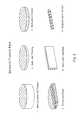
- FIG. 1is a simplified perspective view of a laser device fabricated on a nonpolar substrate according to an embodiment of the present invention
- FIG. 2is a detailed cross-sectional view of a laser device fabricated on a nonpolar substrate according to an embodiment of the present invention
- FIG. 3is a cross-sectional view photograph of a c-direction cleaved facet for a laser device according to an embodiment of the present invention
- FIG. 4is a top-view diagram of a laser device according to an embodiment of the present invention.
- FIGS. 5 to 12illustrate a simplified backend processing method of a laser device according to one or more embodiments of the present invention
- FIG. 13is a simplified diagram illustrating a laser device according to one or more examples of the present invention.
- FIG. 14is a simplified diagram illustrating performance of a 300 mW laser device according to an alternative example of the present invention.
- FIGS. 15 and 16are simplified diagrams illustrating performance of a single-lateral mode blue laser devices with over 21% and 22% [peak] wall plug efficiency (WPE) operating at a wavelength of about 442 nm according to an alternative example of the present invention
- FIG. 17is a simplified diagram illustrating performance of a 550 mW laser device according to an alternative example of the present invention.
- FIG. 18is a detailed plot of pulsed slope efficiency versus threshold current for a plurality of blue lasers having different barrier thicknesses ranging from 1.5 nm to 5.0 nm to demonstrate that lasers characterized with barriers in the 1.5 nm to 2.5 nm range demonstrate lower threshold current and higher slope efficiency according to embodiments of the present invention.
- the present inventionprovides a method and device for emitting electromagnetic radiation using non-polar or semipolar gallium containing substrates such as GaN, AN, InN, InGaN, AlGaN, and AlInGaN, and others.
- the inventioncan be applied to optical devices, lasers, light emitting diodes, solar cells, photoelectrochemical water splitting and hydrogen generation, photodetectors, integrated circuits, and transistors, among other devices.
- FIG. 1is a simplified perspective view of a laser device 100 fabricated on a nonpolar substrate according to an embodiment of the present invention.
- the optical deviceincludes a gallium nitride substrate member 101 having a nonpolar crystalline surface region characterized by an orientation of about ⁇ 2 degrees to about 2 degrees towards (0001) and less than about 0.5 degrees towards (11-20).
- the gallium nitride substrate memberis a bulk GaN substrate characterized by having a nonpolar crystalline surface region, but can be others.
- the bulk GaN substratehas a surface dislocation density below 10 5 cm ⁇ 2 or 10E5 to 10E7 cm ⁇ 2. It should be noted that homoepitaxial growth on bulk GaN is generally better than hetero-epitaxy growth.
- the nitride crystal or wafermay comprise Al x In y Ga 1-x-y N, where 0 ⁇ x, y, x+y ⁇ 1.
- the nitride crystalcomprises GaN.
- the GaN substratehas threading dislocations, at a concentration between about 10 5 cm ⁇ 2 and about 10 8 cm ⁇ 2 , in a direction that is substantially orthogonal or oblique with respect to the surface. As a consequence of the orthogonal or oblique orientation of the dislocations, the surface dislocation density is below about 10 5 cm ⁇ 2 or others such as those ranging from about 10E5-10E8 cm ⁇ 2.
- the devicehas a laser stripe region formed overlying a portion of the nonpolar crystalline orientation surface region.
- the laser stripe regionis characterized by a cavity orientation is substantially parallel to the c-direction.
- the laser stripe regionhas a first end 107 and a second end 109 .
- the devicehas a first cleaved c-face facet provided on the first end of the laser stripe region and a second cleaved c-face facet provided on the second end of the laser stripe region.
- the first cleaved c-facetis substantially parallel with the second cleaved c-facet.
- Mirror surfacesare formed on each of the cleaved surfaces.
- the first cleaved c-facetcomprises a first mirror surface.
- the first mirror surfaceis provided by a scribing and breaking process. The scribing process can use any suitable techniques, such as a diamond scribe or laser scribe or combinations.
- the first mirror surfacecomprises a reflective coating.
- deposition of the reflective coatingoccurs using, for example, electron beam (ebeam) evaporation, thermal evaporation, RF sputtering, DC sputtering, ECR sputtering, ion beam deposition, Ion Assisted Deposition, reactive ion plating, any combinations, and the like.
- the present methodmay provide surface passivation to the exposed cleaved surface prior to coating.
- the reflective coatingis selected from silicon dioxide, hafnia, and titania, tantalum pentoxide, zirconia, including combinations, and the like.
- the reflective coatingis highly reflective and includes a coating of silicon dioxide and tantalum pentoxide, which has been deposited using electron beam deposition.
- the first mirror surfacecan also comprise an anti-reflective coating.
- the second cleaved c-facetcomprises a second mirror surface.
- the second mirror surfaceis provided by a scribing and breaking process according to a specific embodiment.
- the scribingis diamond scribed or laser scribed or the like.
- the second mirror surfacecomprises a reflective coating, such as silicon dioxide, hafnia, titania, tantalum pentoxide, zirconia, combinations, and the like.
- the second mirror surfacecomprises an anti-reflective coating.
- the coatingcan be formed using electron beam deposition, thermal evaporation, RF sputtering, DC sputtering, ECR sputtering, ion beam deposition, ion assisted deposition, reactive ion plating, any combinations, and the like.
- the present methodmay provide surface passivation to the exposed cleaved surface prior to coating.
- the laser stripehas a length and width.
- the lengthranges from about 50 microns to about 3000 microns.
- the stripealso has a width ranging from about 0.5 microns to about 50 microns, but can be other dimensions.
- the stripecan also be about 1 to 20 microns or 1 to 2 microns for a single lateral mode laser device.
- the widthis substantially constant in dimension, although there may be slight variations. The width and length are often formed using a masking and etching process, which are commonly used in the art.
- the deviceis also characterized by a spontaneously emitted light is polarized in substantially perpendicular to the c-direction. That is, the device performs as a laser or the like.
- the spontaneously emitted lightis characterized by a polarization ratio of greater than 0.1 to about 1 perpendicular to the c-direction.
- the spontaneously emitted lightcharacterized by a wavelength ranging from about 400 nanometers to yield a violet emission, a blue emission, a green emission, and others. In other embodiments, the wavelength range is within about 405 nm or slightly more or less.
- the lightcan be emissions ranging from violet 395 to 420 nanometers; blue 430 to 470 nm; green 500 to 540 nm; and others, which may slightly vary depending upon the application.
- the spontaneously emitted lightis in the wavelength range of 430 nm and greater and is highly polarized with a polarization ratio of greater than 0.4.
- the spontaneous polarization ratiois greater than 0.3 for an emission polarized perpendicular to the c-direction for a spontaneous emission peak wavelength greater than 430 nm.
- the emitted lightis characterized by a polarization ratio that is desirable.
- FIG. 2is a detailed cross-sectional view of a laser device 200 fabricated on a nonpolar substrate according to an embodiment of the present invention.
- the laser deviceincludes gallium nitride substrate 203 , which has an underlying n-type metal back contact region 201 .
- the metal back contact regionis made of a suitable material such as those noted below and others.
- the devicealso has an overlying n-type gallium nitride layer 205 , an active region 207 , and an overlying p-type gallium nitride layer structured as a laser stripe region 211 . Additionally, the device also includes an n-side separate confinement hetereostructure (SCH) 206 , p-side guiding layer or SCH 208 , p-AlGaN EBL 209 , among other features. In a specific embodiment, the device also has a p++ type gallium nitride material 213 to form a contact region.
- SCHn-side separate confinement hetereostructure
- the p++ type contact regionhas a suitable thickness and may range from about 10 nm 50 nm, or other thicknesses.
- the doping levelcan be higher than the p-type cladding region and/or bulk region.
- the p++ type regionhas doping concentration ranging from about 10E19 to 10E21 Mg/centimeter 3 , and others.
- the p++ type regionpreferably causes tunneling between the semiconductor region and overlying metal contact region.
- each of these regionsis formed using at least an epitaxial deposition technique of metal organic chemical vapor deposition (MOCVD), molecular beam epitaxy (MBE), or other epitaxial growth techniques suitable for GaN growth.
- MOCVDmetal organic chemical vapor deposition
- MBEmolecular beam epitaxy
- the epitaxial layeris a high quality epitaxial layer overlying the n-type gallium nitride layer.
- the high quality layeris doped, for example, with Si or O to form n-type material, with a dopant concentration between about 10 16 cm ⁇ 3 and 10 20 cm ⁇ 3 .
- an n-type Al u In v Ga 1-u-v N layerwhere 0 ⁇ u, v, u+v ⁇ 1, is deposited on the substrate.
- the carrier concentrationmay lie in the range between about 10 16 cm ⁇ 3 and 10 20 cm ⁇ 3 .
- the depositionmay be performed using metalorganic chemical vapor deposition (MOCVD) or molecular beam epitaxy (MBE).
- the bulk GaN substrateis placed on a susceptor in an MOCVD reactor.
- the susceptoris heated to a temperature between about 900 to about 1200 degrees Celsius in the presence of a nitrogen-containing gas.
- the carriercan be hydrogen or nitrogen or others.
- the susceptoris heated to approximately about 900 to about 1100 degrees Celsius under flowing ammonia.
- a flow of a gallium-containing metalorganic precursor, such as trimethylgallium (TMG) or triethylgallium (TEG)is initiated, in a carrier gas, at a total rate between approximately 1 and 50 standard cubic centimeters per minute (sccm).
- the carrier gasmay comprise hydrogen, helium, nitrogen, or argon.
- the ratio of the flow rate of the group V precursor (e.g., ammonia) to that of the group III precursor (trimethylgallium, triethylgallium, trimethylindium, trimethylaluminum) during growthis between about 2000 and about 12000.
- a flow of disilane in a carrier gas, with a total flow rate of between about 0.1 and 10 sccmis initiated.
- the laser stripe regionis made of the p-type gallium nitride layer 211 .
- the laser stripeis provided by an etching process selected from dry etching or wet etching.
- the etching processis dry, but can be others.
- the dry etching processis an inductively coupled plasma (ICP) process using chlorine bearing species or a reactive ion etching (RIE) process using similar chemistries or combination of ICP and RIE, among other techniques.
- ICPinductively coupled plasma
- RIEreactive ion etching
- the chlorine bearing speciesare commonly derived from chlorine gas or the like.
- the devicealso has an overlying dielectric region, which exposes 213 contact region, which is preferably a p++ gallium nitride region.
- the dielectric regionis an oxide such as silicon dioxide or silicon nitride, but can be others, such as those described in more detail throughout the present specification and more particularly below.
- the contact regionis coupled to an overlying metal layer 215 .
- the overlying metal layeris a multilayered structure containing gold and platinum (Pt/Au) or nickel and gold (Ni/Au), but can be others.
- the Ni/Auis formed via electro-beam deposition, sputtering, or any like techniques.
- the thicknessincludes nickel material ranging in thickness from about 50 to about 100 nm and gold material ranging in thickness from about 1000 Angstroms to about 1-3 microns, and others.
- the dielectric regioncan be made using a suitable technique.
- the techniquemay include reactively sputter of SiO2 using an undoped polysilicon target (99.999% purity) with O2 and Ar.
- the techniqueuses RF magnetron sputter cathodes configured for static deposition; sputter target; throw distance; pressure: 1-5 mT or about 2.5 mT, power: 300 to 400 W; flows: 2-3.-9 sccm O2, 20-50 sccm, Ar, deposition thickness: 1000-2500 A, and may include other variations.
- depositionmay occur using non-absorbing, nonconductive films, e.g., Al2O3, Ta2O5, SiO2, Ta2O5, ZrO2, TiO2, HfO2, NbO2.
- the dielectric regionmay be thinner, thicker, or the like.
- the dielectric regioncan also include multilayer coatings, e.g., 1000 A of SiO2 capped with 500 A of Al2O3.
- Deposition techniquescan include, among others, ebeam evaporation, thermal evaporation, RF Sputter, DC Sputter, ECR Sputter, Ion Beam Deposition, Ion Assisted Deposition, reactive ion plating, combinations, and the like.
- the laser devicehas active region 207 .
- the active regioncan include one to twenty quantum well regions according to one or more embodiments.
- an active layeris deposited.
- the active layermay comprise a single quantum well or a multiple quantum well, with 1-20 quantum wells.
- the active layermay include about 3-7 quantum wells or more preferably 4-6 quantum wells or others.
- the quantum wellsmay comprise InGaN wells and GaN or InGaN barrier layers.
- the well layers and barrier layerscomprise Al w In x Ga 1-w-x N and Al y In z Ga 1-y-z N, respectively, where 0 ⁇ w, x, y, z, w+x, y+z ⁇ 1, where w ⁇ u, y and/or x>v, z so that the bandgap of the well layer(s) is less than that of the barrier layer(s) and the n-type layer.
- the well layers and barrier layersmay each have a thickness between about 1 nm and about 40 nm. In a preferred embodiment, each of the thicknesses is preferably 1-8 nm.
- each well regionmay have a thickness of about 4 nm to 6 nm and each barrier region may have a thickness of about 1 nm to about 5 nm, among others.
- each well regionmay have a thickness of about 4 nm to 6 nm and each barrier region may have a thickness of about 1 nm to about 3 nm, among others.
- each well regionmay have a thickness of about 2.5 nm to 4.5 nm and each barrier region may have a thickness of about 2 nm to about 4 nm, among others.
- the active layercomprises a double heterostructure, with an InGaN or Al w In x Ga 1-w-x N layer about 10 nm to 100 nm thick surrounded by GaN or Al y In z Ga 1-y-z N layers, where w ⁇ u, y and/or x>v, z.
- the composition and structure of the active layerare chosen to provide light emission at a preselected wavelength.
- the active layermay be left undoped (or unintentionally doped) or may be doped n-type or p-type.
- the active regioncan also include an electron blocking region, and a separate confinement heterostructure.
- the separate confinement heterostructurecan include AlInGaN or preferably InGaN, but can be other materials.
- the SCHis generally comprised of material with an intermediate index between the cladding layers and the active layers to improve confinement of the optical mode within the active region of the laser device according to a specific embodiment.
- the SCH layershave a desirable thickness, impurity, and configuration above and below the active region to confine the optical mode.
- the upper and lower SCHcan be configured differently or the same.
- the electron blocking regioncan be on either side or both sides of the SCH positioned above the active region according to a specific embodiment.
- the lower SCHcan range from about 10 nm to about 150 nm, and preferably about 40 to 120.
- the lower SCHis preferably InGaN having with about 2% to about 10% indium by atomic percent according to a specific embodiment.
- the upper SCH region thicknessranges from about 10 to 150 nm, and preferably about 10 nm to 50 nm.
- the upper SCHis preferably GaN or InGaN having about 0% to about 5% indium by atomic percent according to a specific embodiment. In the case that that there is no indium in this upper layer, the layer can be referred to as an p-side guiding layer that is comprised of GaN.
- an electron blocking layeris preferably deposited.
- the electron blocking layercomprises a gallium and nitrogen containing material including magnesium 10E16 cm ⁇ 3 to about 10E22 cm ⁇ 3.
- the electron-blocking layermay comprise Al s In t Ga 1-s-t N, where 0 ⁇ s, t, s+t ⁇ 1, with a higher bandgap than the active layer, and may be doped p-type.
- the electron blocking layercomprises AlGaN with an Al composition ranging from 10 to 20%.
- the electron blocking layercomprises AlGaN with an Al composition ranging from 3 to 10%.
- the electron blocking layermay not contain Al.
- the electron blocking layercomprises an AlGaN/GaN super-lattice structure, comprising alternating layers of AlGaN and GaN, each with a thickness between about 0.2 nm and about 5 nm.
- the AlGaN blocking layeris replaced by a GaN layer doped with magnesium from about 10E16 cm ⁇ 3 to about 10E22 cm ⁇ 3.
- the present inventionprovides a laser device and related methods using thin barrier materials to achieve improved performance.
- a nonpolar blue laser with multi-quantum well (MQW) active regionscomprised of 4-7 QWs with thicknesses in the 4 to 6 nm range
- barrier thicknesses in the 1.5 nm to 2.5 nm rangeprovide the lowest threshold current, highest slope efficiency, and lower forward voltage.
- Blue laser diodes employing such MQW active regions with 3 or more, or 5 or more QWs fabricated on conventional c-plane GaNwould be impractical due to the high strain accumulation, which would likely lead to the onset of defects.
- the ultra-thin barriercan be 1.0 nm and less, although there can be some variations. In other embodiments, the ultra-thin barrier can be 2.5 nm and less or 2.0 nm and less. This results in higher optical overlap of the electric field and the quantum wells within the laser. Since the modal gain of a laser is given by the product of the material gain and the optical confinement, this increase in the optical confinement results in increased modal gain. Increased gain reduces the threshold current density, and hence reduces the threshold current in a laser with a given cavity dimension.
- Thin barrierscan further increase the laser performance by again increasing the modal gain and by reducing absorption losses in the quantum wells by promoting a more uniform carrier distribution throughout the quantum wells according to a specific embodiment.
- the heavy effective mass of holestypically limits carrier transport in multi-quantum well InGaN-based devices. With a reduced total transport length from the p-side of the active region where holes are injected to the lower quantum wells towards the n-side, holes are more readily able to travel to the lowest quantum wells before recombining with an electron.
- Such thin barriersincrease the probability for holes to tunnel through the barriers such that they do not need to overcome the potential energy of the hole/barrier hetereointerface. This again promotes more uniform carrier filling of the quantum wells.
- This more uniform carrier distribution profileassures that no wells are left un-pumped such that they are absorbing or lossy to the optical mode.
- the higher loss associated with insufficiently pumped wellsleads to an increased threshold current and a decreased slope efficiency.
- the carrier uniformityprevents the case where a majority of the carriers are recombining in only some of the quantum wells such that the carrier concentration would become very high in those wells and the gain would saturate.
- a uniform carrier distributionguarantees that each quantum well is kept as far from gain saturation as possible for a given laser injection current.
- a reduced transport length and a higher probability for carrier tunneling through the barrierscould also reduce the forward voltage of the laser diode.
- thin barrierscan also be employed.
- 4 to 5 quantum wells with thicknesses that range from 3 nm to 4.5 nm and barriers that range in thickness from 2 nm to 4.5 nmcan be employed.
- the p-type gallium nitride structurewhich can be a p-type doped Al q In r Ga 1-q-r N, where 0 ⁇ q, r, q+r ⁇ 1, layer is deposited above the active layer.
- the p-type layermay be doped with Mg, to a level between about 10 16 cm ⁇ 3 and 10 22 cm ⁇ 3 , and may have a thickness between about 5 nm and about 1000 nm.
- the outermost 1-50 nm of the p-type layermay be doped more heavily than the rest of the layer, so as to enable an improved electrical contact.
- the laser stripeis provided by an etching process selected from dry etching or wet etching. In a preferred embodiment, the etching process is dry, but can be others.
- the devicealso has an overlying dielectric region, which exposes 213 contact region. In a specific embodiment, the dielectric region is an oxide such as silicon dioxide.
- the metal contactis made of suitable material.
- the reflective electrical contactmay comprise at least one of silver, gold, aluminum, nickel, platinum, rhodium, palladium, chromium, or the like.
- the electrical contactmay be deposited by thermal evaporation, electron beam evaporation, electroplating, sputtering, or another suitable technique.
- the electrical contactserves as a p-type electrode for the optical device.
- the electrical contactserves as an n-type electrode for the optical device.
- a ridge waveguideis fabricated using a certain deposition, masking, and etching processes.
- the maskis comprised of photoresist (PR) or dielectric or any combination of both and/or different types of them.
- PRphotoresist
- the ridge maskis 1 to 2.5 microns wide for single lateral mode applications or 2.5 to 30 um wide for multimode applications.
- the ridge waveguideis etched by ion-coupled plasma (ICP), reactive ion etching (RIE), or other method.
- ICPion-coupled plasma
- RIEreactive ion etching
- the etched surfaceis 25-250 nm above the active region.
- a dielectric passivation layeris then blanket deposited by any number of commonly used methods in the art, such as sputter, e-beam, PECVD, or other methods.
- This passivation layercan include SiO2, Si3N4, Ta2O5, or others.
- the thickness of this layeris 80-400 nm thick.
- An ultrasonic processis used to remove the etch mask which is covered with the dielectric. This exposes the p-GaN contact layer.
- P-contact metalis deposited by e-beam, sputter, or other deposition technique using a PR mask to define the 2D geometry.
- the contact layercan be Ni/Au but others can be Pt/Au or Pd/Au.
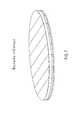
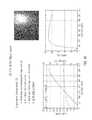
- FIG. 3is a cross-sectional view photograph of a c-direction cleaved facet for a laser device according to an embodiment of the present invention.
- This diagramis merely an example, which should not unduly limit the scope of the claims herein.
- One of ordinary skill in the artwould recognize other variations, modifications, and alternatives.
- the c-direction cleaved facetis smooth and provides a suitable mirror surface.
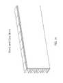
- FIG. 4is a top-view diagram of a laser device according to an embodiment of the present invention.
- This diagramis merely an example, which should not unduly limit the scope of the claims herein.
- the laser stripeis configured in the c-direction, which has a projection normal to the c-direction.
- the top-view of the gallium nitride substrateis of a slight mis-cut or off-cut surface region orientation according to a specific embodiment.
- a method of processing a laser devicemay be outline as follows, see also FIG. 5 :
- processed substrateincluding laser devices with ridges
- the above sequence of stepsis used to form individual laser devices on a die from a substrate structure according to one or more embodiments of the present invention.
- the methodincludes cleaved facets substantially parallel to each other and facing each other in a ridge laser device configured on a non-polar gallium nitride substrate material.
- one or more of these stepscan be combined, or removed, or other steps may be added without departing from the scope of the claims herein.
- One of ordinary skill in the artwould recognize other variations, modifications, and alternatives.
- FIG. 6is a simplified illustration of a substrate thinning process according to an embodiment of the present invention.
- the methodbegins with a gallium nitride substrate material including laser devices and preferably ridge laser devices, but can be others.
- the substratehas been subjected to frontside processing according to a specific embodiment. After frontside processing has been completed, one or more of the GaN substrates are mounted onto a sapphire carrier wafer or other suitable member.
- the methoduses Crystalbond 509, which is a conventional mounting thermoplastic.
- the thermoplasticcan be dissolved in acetone or other suitable solvent.
- the carrier waferis mounted to a lapping jig.
- lapping jigAn example of such lapping jig is made by Logitech Ltd. of the United Kingdom, or other vendor.
- the lapping jighelps maintain planarity of the substrates during the lapping process according to a specific embodiment.
- the starting thickness of the substratesare ⁇ 325 um+/ ⁇ 20 um, but can be others, e.g., 250 to about 500 um.
- the methodlaps or thins the substrates down to 60-70-80 um thickness, but can also be thinner or slightly thicker.
- the lapping jigis configured with a lapping plate, which is often made of a suitable material such as cast iron configured with a flatness of less than 5 um, but can be others.
- the methoduses a lapping slurry that is 1 part silicon carbide (SiC) and 10 parts water, but can also be other variations.
- the SiC gritis about 5 um or 9 micron and others in dimension.
- the lapping plate speedis suitable at about 10 revolutions per minute.
- the methodcan adjust the lapping jig's down pressure to achieve a desired lapping rate, such as 2-3 um/min or greater or slightly less according to one or more embodiments.
- the present methoduses a suitable lapping process.
- a suitable lapping processincludes use of a Logitech LP50 lapping/polishing system using a suitable slurry mixture.
- the slurrymay include a SiC slurry such as 9 um SiC slurry (from Logitech), among others.
- the slurrymay be mixed with a SiC to water ratio such as 1:10 SiC:H2O, or others, e.g., 1-3:8-12.
- the lappingoccurs at about 5 to about 50 rpm and is preferably about 10 rpm, which achieves a removal rate of about 1-5 um/min removal rate. Lapping occurs until the thickness of the substrate is about 80 um or 75 um and less.
- grin dingmay be used to replace or supplement lapping.
- Other variationsinclude other lapping materials and grits, such as Al2O3, diamond, boron nitride, combinations, and others.
- Grit sizecan also range from about 1 um, 3 um, 5 um, 15 um, combinations, and others. Lapping is often followed by polishing, which will be described in more detail below.
- the present methoduses a suitable polishing process.
- polishingoccurs using the Logitech LP50 lapping/polishing system.
- diamond polishing materialincludes a 1 um diamond suspension (from Eminess) configured on a polish pad, e.g., SUBA IV, 40-80 rpm or 70 rpm, but can be others.
- the polishingoccurs to achieve a 3-5 um/hr removal rate and removes about 5 to 10 microns of substrate material, which leaves the substrate thickness at about 65 um. In other embodiments, polishing may be optional.
- the present methodincludes a lapping process that may produce subsurface damage in the GaN material to cause generation of mid level traps or the like.
- the midlevel trapsmay lead to contacts having a Schottky characteristic.
- the present methodincludes one or more polishing processes such that ⁇ 10 um of material having the damage is removed according to a specific embodiment.
- the methoduses a PolitexTM polishing pad of Rohm and Haas, but can be others, that is glued onto a stainless steel plate.
- a polishing solutionis Ultrasol300K manufactured by Eminess Technologies, but can be others.
- the Ultra-Sol 300Kis a high-purity colloidal silica slurry with a specially designed alkaline dispersion.
- the methodincludes a polishing rate of about ⁇ 2 um/hour, but can be others, which are higher or lower.
- the present inventionprovides a method for achieving high quality n-type contacts for m-plane GaN substrate material.
- the methodprovides contacts that are rough to achieve suitable ohmic contact.
- the roughnesscauses exposure of other crystal planes, which lead to good contacts.
- the present methodincludes a lapped surface, which is rough in texture to expose more than one or multiple different crystal planes.
- lappingmay be followed by etching such as dry etching with (Cl2/BCl3)/SiCl4/Cl2 based chemistries and/or wet etching.
- etchingremoves the subsurface damage, however, it is likely not to planarize the surface like polishing.
- FIG. 7is a simplified diagram illustrating a backside n-contact method according to one or more embodiments. This diagram is merely an illustration and should not unduly limit the scope of the claims herein. One of ordinary skill in the art would recognize other variations, modifications, and alternatives.
- the methodforms n-contacts on the backside of the substrates according to one or more embodiments. At this point, the thinned substrates are still mounted to and maintained on the sapphire wafer. In a preferred embodiment, the thinned substrates are “batch process” for efficiency and handling. In a specific embodiment, the method using batch processing helps prevent any damage associated with handling very thin (60-80 um) substrates.
- the backside contact regionsare formed using laser irradiation as a pre-treatment before contact formation.
- the laser irradiationcan be performed using a scribing process by way of laser irradiation. An example is described in U.S. Ser. No. 61/345,561, which is commonly assigned, and hereby incorporated by reference.
- the backside contactincludes about 300 ⁇ Al/3000 ⁇ Au or other suitable materials.
- the contactis a stack of metals that are deposited by e-beam evaporation or other suitable techniques.
- the contactscan include aluminum/nickel/gold materials having respective thicknesses of, for example, 300/1000/3000 Angstroms or Ti/Pt/Au materials having respective thicknesses of, for example, 200/400/3000 Angstroms, or others.
- the methodincludes use of a wet etch such as a hydrofluoric acid or hydrochloric wet etch to remove any oxides on the surface.
- the metal stackis preferably not annealed or subjected to high temperature processing after its formation. In other embodiments, the metal stack may be annealed directly or indirectly via radiation, conduction, convection, or combinations thereof.
- FIG. 8is a simplified diagram illustrating a scribe and break operation according to one or more embodiments. This diagram is merely an illustration and should not unduly limit the scope of the claims herein. One of ordinary skill in the art would recognize other variations, modifications, and alternatives.
- the substratesare demounted from the sapphire carrier wafer and cleaned in acetone and isopropyl alcohol according to a specific embodiment.
- the substratesare then mounted onto vinyl tape for the scribe and break process depending upon the embodiment.
- the vinyl tapeis non-tacky or other suitable configuration.
- the tapedoes not leave any residue on the laser bars, which are substantially free from such residues, which are often polymeric in nature or particulates. In other embodiments, there may be some residual material from the tape that is preferably removed.
- the present methodperforms a cleaning process to remove residual material from the substrate. After demounting the substrate from the tape, residue is often leftover from wax or other adhesive material from the tape.
- the methodremoves the residue using at least a de-scum process.
- the de-scum processcan include an oxygen plasma from an inductively coupled plasma using an oxygen species, e.g., O2.
- An example of such processuses an Oxford ICP 180, a vacuum pressure ranging in the millitorr range, such as 20 mT, a flow rate of oxygen from about 10 sccm to about 100 sccm, and preferably about 50 sccm of O 2 gas.
- the ICPuses RF power ranging from about 50 W to about 300 W ICP for a suitable amount of time and preferably about 10 minutes to remove the wax material.
- Other plasma processessuch as reactive ion etching, barrel ashing, down stream ashing, and others may also be used.
- the methodincludes one or more scribing processes.
- the methodincludes subjecting the substrates to a laser for pattern formation.
- the patternis configured for the formation of a pair of facets for one or more ridge lasers.
- the pair of facetsface each other and are in parallel alignment with each other.
- the methoduses a UV (355 nm) laser to scribe the laser bars.
- the laseris configured on a system, which allows for accurate scribe lines configured in one or more different patterns and profiles.
- the scribingcan be performed on the backside, frontside, or both depending upon the application.
- the methoduses backside scribing or the like.
- the methodpreferably forms a continuous line scribe that is perpendicular to the laser bars on the backside of the GaN substrate.
- the scribeis generally 15-20 um deep or other suitable depth.
- backside scribingcan be advantageous. That is, the scribe process does not depend on the pitch of the laser bars or other like pattern. Accordingly, backside scribing can lead to a higher density of laser bars on each substrate according to a preferred embodiment. In a specific embodiment, backside scribing, however, may lead to residue from the tape on one or more of the facets.
- backside scribeoften requires that the substrates face down on the tape.
- front-side scribingthe backside of the substrate is in contact with the tape.
- front side scribingmay be used for die separation.
- the present methodperforms a cleaning process to remove residual material from the substrate. After demounting the substrate from the tape, residue is often leftover from wax or other adhesive material from the tape.
- the methodremoves the residue using at least a de-scum process.
- the de-scum processcan include an oxygen plasma from an inductively coupled plasma using an oxygen species, e.g., O2.
- An example of such processuses an Oxford ICP 180, a vacuum pressure ranging in the millitorr range, such as 20 mT, a flow rate of oxygen from about 10 sccm to about 100 sccm, and preferably about 50 sccm of O 2 gas.
- the ICPuses RF power ranging from about 50 W to about 300 W ICP for a suitable time or preferably about 10 minutes to remove the wax material.
- Other plasma processessuch as reactive ion etching, barrel ashing, down stream ashing, and others may also be used.
- the present methoduses frontside scribing, which facilitates formation of clean facets.
- the frontside scribing processis preferably used.
- the methodincludes a scribe pattern to produce straight cleaves with minimal facet roughness or other imperfections. Further details of scribing are provided below.
- the pitch of the laser maskcan be about 200 um, but can be others.
- the methoduses a 170 um scribe with a 30 um dash.
- the scribe lengthis maximized or increased while maintaining the heat affected zone of the laser away from the laser ridge, which is sensitive to heat.
- Scribe ProfileA saw tooth profile generally produces minimal facet roughness. It is believed that the saw tooth profile shape creates a very high stress concentration in the material, which causes the cleave to propogate much easier and/or more efficiently.
- the profilemay be a shallow scribe, which produces a recessed region. The shallow scribe ranges from about 3 to 10 microns and is preferably about 4 to 7 microns depending upon the specific embodiment.
- the present methoduses an Opto Laser Scriber configured with a 355 nm laser or other suitable source.
- the laseroutputs selected pulses to form a desirable scribe characterized with a skip.
- the scribegenerally has a constant depth of ⁇ 5-10 um but can be others.
- the scriberalso has a power of 100 mW to about 300 mW or other suitable power and has a beam moving at about 25 to about 100 mm/s, but can be slightly more or less, or other speeds.
- the methodalso performs a slag removal process to remove the slag from the laser scribe using wet chemistry, e.g., 0.5-1.5:2.5-3.5 or 1:3, HNO 3 : HCl, but can be others.
- the slag removal processimproves the laser and its cleanliness in a preferred embodiment.
- the methodcan use different laser configurations (e.g., different wavelength, different pulse frequency), a mechanical scribing process (e.g, diamond scribing), or deep etching using wet and/or dry techniques.
- the present methodprovides for a scribe suitable for fabrication of the present laser devices.
- FIG. 9illustrates cross-sections of substrate materials associated with (1) a backside scribe process; and (2) a frontside scribe process.
- the methodincludes a breaking process to form a plurality of bar structures.
- This diagramis merely an illustration and should not unduly limit the scope of the claims herein.
- the methoduses a breaker to cleave the substrates into bars.
- the breakerhas a metal support that has a gap spacing of 900 um for 600 micron long laser cavities.
- the substrateis positioned over the support so that the scribe line is in the centered.
- a suitably sharp ceramic bladethen applies pressure directly on the scribe line causing the substrate to cleave along the scribe line.
- FIG. 11is a simplified diagram illustrating a stacking and coating process according to one or more embodiments. Again, this diagram is merely an illustration and should not unduly limit the scope of the claims herein. One of ordinary skill in the art would recognize other variations, modifications, and alternatives.
- the front facet coating filmscan be selected from any suitable low reflectance design (AR design).
- the AR designincludes a quarterwave coating of Al 2 O 3 capped with a thin layer of HfO 2 according to a specific embodiment.
- the Al 2 O 3 coatingis a robust dielectric, and HfO 2 is dense, which helps environmentally passivate and tune the reflectance of the front facet.
- These coating filmsare preferably deposited by e beam evaporation. Other examples include thermal evaporation, RF sputtering, DC sputtering, ECR sputtering, ion beam deposition, Ion Assisted Deposition, reactive ion plating, any combinations, and the like.
- the present methodmay provide surface passivation to the exposed cleaved surface prior to coating.
- the back facetis coated with a high reflectance HR design.
- the HR designincludes several quarterwave pairs of SiO 2 /HfO 2 .
- the HR designincludes several quarterwave layer pairs of SiO2/Ta2O5 or other suitable materials. In a specific embodiment, roughly 6-7 pairs may be used to achieve a reflectance over 99%.
- the methoduses a suitable deposition system configured for deposition of each of the facets without breaking vacuum.
- the deposition systemincludes a dome structure with sufficient height and spatial volume.
- the systemallows for the plurality of bars configured in a fixture to be flipped from one side to another side and to expose the back facet and the front facet according to a specific embodiment.
- the methodallows for first deposition of the back facet, reconfiguring the bar fixture to expose the front facet, and second deposition of the front facet without breaking vacuum.
- the methodallows for deposition of one or more films on front and back without breaking vacuum to save time and improve efficiency. Other embodiments can break vacuum.
- FIG. 12illustrates a method directed to singulate bars into a plurality of die according to a specific embodiment.
- This diagramis merely an illustration and should not unduly limit the scope of the claims herein.
- the methodincludes testing the laser devices in bar form prior to die singulation.
- the methodsingulates the bars by performing a scribe and break process (similar to the facet cleave).
- the methodforms a shallow continuous line scribe on the top side of the laser bar according to a specific embodiment.
- the width of each dieis about 200 um, which may reduce the support gap to 300 um or so.
- the tapeis expanded and each of the die is picked off of the tape.
- the methodperforms a packing operation for each of the die according to one or more embodiments.
- FIG. 13is a simplified diagram illustrating a laser device according to one or more examples of the present invention.
- the optical deviceincludes a gallium nitride substrate member having a nonpolar crystalline surface region characterized by an orientation of about +/ ⁇ 1 degree towards (0001) and less than about 0.3 degrees towards (11-20).
- the bulk GaN substratehas a surface dislocation density below 1E5 to 1E7 cm ⁇ 2 or about 1E6 cm ⁇ 2 and a surface roughness of less than 0.2 nm.
- the devicehas a laser stripe region formed overlying a portion of the nonpolar crystalline orientation surface region.
- the laser stripe regionis characterized by a cavity orientation is substantially parallel to the c-direction and has a first end and a second end.
- the devicehas a first cleaved c-face facet provided on the first end of the laser stripe region and a second cleaved c-face facet provided on the second end of the laser stripe region.
- the first cleaved c-facetis substantially parallel with the second cleaved c-facet.
- Mirror surfacesare formed on each of the cleaved surfaces.
- the first cleaved c-facetcomprises a first mirror surface.
- the first mirror surfaceis provided by a scribing and breaking process such as the one described herein.
- the first mirror surfacecomprises a reflective coating, which is alumina and hafnia.
- the coatingmay include combinations of SiO2/Ta2O5, among other materials, and the like.
- the second cleaved c-facetcomprises a second mirror surface.
- the second mirror surfaceis provided by a scribing and breaking process such as the one described herein.
- the second mirror surfacecomprises a reflective coating, such as silicon dioxide and hafnia.
- the laser stripehas a length and width. The length is 400-1000 ⁇ m and the width is 1-1.4-4 ⁇ m. The width is substantially constant in dimension.
- the facetsare configured in a desirable manner. That is, one of the facets is substantially free from coating and is generally exposed GaN material having a reflectance ⁇ 18.4% or more generally from about 10% to about 24%, but can be others.
- the other facetis coated with a reflective material.
- the reflective materialmay be ⁇ /2 coatings of non-absorbing film materials to maintain the same or similar reflectance. Examples of materials include, among others, Al2O3, Ta2O5, SiO2, Ta2O5, ZrO2, TiO2, HfO2, NbO2, or others. In other embodiments, multilayer coatings using combinations of the above materials achieve the same reflectance.
- the coatingsinclude single layer coatings with varying reflectances, multilayer coatings with varying reflectances, or others.
- coatingsmay be deposited using similar or different processes and/or tools.
- processesinclude e-beam evaporation, thermal evaporation, RF sputtering, DC sputtering, ECR sputtering, ion beam deposition, Ion Assisted Deposition, reactive ion plating, any combinations, and the like.
- the present methodmay provide surface passivation to the exposed cleaved surface prior to coating.
- the deviceis also characterized by a spontaneously emitted light is polarized in substantially perpendicular to the c-direction. That is, the device performs as a laser.
- the spontaneously emitted lightis characterized by a polarization ratio perpendicular to the c-direction.
- the spontaneously emitted lightcharacterized by a wavelength of about 405 nanometers to yield blue-violet emission.
- the graphillustrates a power and current relationship for the subject laser device at about 25 Degrees Celsius. Additionally, the wavelength is indicated at about 405 nanometers for the subject laser device.
- the present deviceuses thin barrier regions configured in the active region, which has been described throughout the present specification and more particularly below.
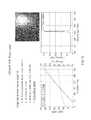
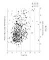
- FIG. 14is a simplified diagram illustrating performance of a 300 mW single-lateral mode blue laser device operating at a wavelength of 446 nm according to an alternative example of the present invention.
- This diagramis merely an illustration and should not unduly limit the scope of the claims herein.
- One of ordinary skill in the artwould recognize other variations, modifications, and alternatives.
- As shownare continuous wave (CW) optical output power plotted against input current and voltage along with a plot of optical intensity plotted against wavelength.
- the light power output plotted against input current and voltageprovides an efficiency of 17.5% at 145 mW for the 300 mW CW blue laser device.
- the current and voltage thresholdsare also shown.
- the present deviceuses thin barrier regions configured in the active region, which has been described throughout the present specification and more particularly below.
- the laser deviceis single mode and has been fabricated using the process and structures described herein.
- FIGS. 15 and 16are simplified diagrams illustrating performance of a single-lateral mode blue laser devices with over 21% [peak] wall plug efficiency (WPE) operating at a wavelength of about 442 nm according to an alternative example of the present invention.
- WPEwall plug efficiency
- FIGS. 15 and 16are simplified diagrams illustrating performance of a single-lateral mode blue laser devices with over 21% [peak] wall plug efficiency (WPE) operating at a wavelength of about 442 nm according to an alternative example of the present invention.
- WPEwall plug efficiency
- the single-lateral-mode blue laser device in FIG. 15achieves a peak WPE of 21% at an output power of about 130 mW in a specific embodiment.
- the single-lateral-mode blue laser device in FIG. 14achieves a peak WPE of 22.7% at an output power of about 170 mW according to a specific embodiment.
- Such WPE values from single lateral mode blue lasersrepresent state-of-the-art performance.
- the current and voltage thresholdsare also shown.
- the laser deviceis single mode and has been fabricated using the process and structures described herein.
- FIG. 17is a simplified diagram illustrating performance of a CW 550 mW single lateral mode blue laser device according to an alternative example of the present invention.
- This diagramis merely an illustration and should not unduly limit the scope of the claims herein.
- One of ordinary skill in the artwould recognize other variations, modifications, and alternatives.
- optical output power plotted against input current for a 550 mW CW laser deviceAs shown are optical output power plotted against input current for a 550 mW CW laser device.
- the light power output plotted against current inputprovides an efficiency of 16.7% at 220 mW for the single lateral mode CW blue laser device.
- the devicehas a threshold current of 35 mA, a threshold voltage of 4.1 V, and outputs over 500 mW with about 500 mA of input current.
- Such output powers in the 500 mW rangerepresents state-of-the-art performance from single lateral mode blue laser device.
- the laserhas been fabricated using the process and structures described herein.
- the present inventionprovides a laser device and related methods using thin barrier materials to achieve improved performance.
- conventional laser diodes fabricated on c-plane GaNtypically employ barrier thicknesses in the 6 nm to 12 nm and greater range.
- the performance of laser diodes fabricated on nonpolar and semipolar substratescan be improved by implementing ultra thin barriers according to the present embodiment, as further described by illustration in FIG. 18 .
- nonpolar blue laser with multi-quantum well (MQW) active regionscomprised of 4-7 QWs with thicknesses in the 4 to 6 nm range
- barrier thicknesses in the 1.5 nm to 2.5 nm rangeprovide the lowest threshold current, highest slope efficiency, and lower forward voltage according to a preferred embodiment.
- Blue laser diodes employing such MQW active regions with 3 or more, or 5 or more QWs fabricated on conventional c-plane GaNwould be impractical due to the high strain accumulation, which would likely lead to the onset of defects, as noted.
- the outer quantum wells within the active regionare pushed in towards the peak of the optical mode, as also explained herein. This results in higher optical overlap of the electric field and the quantum wells within the laser. Since the modal gain of a laser is given by the product of the material gain and the optical confinement, this increase in the optical confinement results in increased modal gain. Increased gain reduces the threshold current density, and hence reduces the threshold current in a laser with a given cavity dimension.
- Thin barrierscan further increase the laser performance by again increasing the modal gain and by reducing absorption losses in the quantum wells by promoting a more uniform carrier distribution throughout the quantum wells according to a specific embodiment.
- the heavy effective mass of holestypically limits carrier transport in multi-quantum well InGaN-based devices. With a reduced total transport length from the p-side of the active region where holes are injected to the lower quantum wells towards the n-side, holes are more readily able to travel to the lowest quantum wells before recombining with an electron.
- Such thin barriersincrease the probability for holes to tunnel through the barriers such that they do not need to overcome the potential energy of the hole/barrier hetereointerface. This again promotes more uniform carrier filling of the quantum wells.
- This more uniform carrier distribution profileassures that no wells are left un-pumped such that they are absorbing or lossy to the optical mode.
- the higher loss associated with insufficiently pumped wellsleads to an increased threshold current and a decreased slope efficiency.
- the carrier uniformityprevents the case where a majority of the carriers are recombining in only some of the quantum wells such that the carrier concentration would become very high in those wells and the gain would saturate.
- a uniform carrier distributionguarantees that each quantum well is kept as far from gain saturation as possible for a given laser injection current.
- a reduced transport length and a higher probability for carrier tunneling through the barrierscould also reduce the forward voltage of the laser diode.
- thin barrierscan also be employed.
- 4 to 5 quantum wells with thicknesses that range from 3 nm to 4.5 nm and barriers that range in thickness from 2 nm to 4.5 nmcan be employed.
- the present inventionincludes a device and method configured on other gallium and nitrogen containing substrate orientations.
- the gallium and nitrogen containing substrateis configured on a family of planes including a ⁇ 20-21 ⁇ crystal orientation.
- ⁇ 20-21 ⁇is 14.9 degrees off of the m-plane towards the c-plane (0001).
- the miscut or off-cut angleis +/ ⁇ 17 degrees from the m-plane towards c-plane or alternatively at about the ⁇ 20-21 ⁇ crystal orientation plane.
- the present deviceincludes a laser stripe oriented in a projection of the c-direction, which is perpendicular to the a-direction (or alternatively on the m-plane, it is configured in the c-direction).
- the cleaved facetwould be the gallium and nitrogen containing face (e.g., GaN face) that is +/ ⁇ 5 degrees from a direction orthogonal to the projection of the c-direction (or alternatively, for the m-plane laser, it is the c-face).
- the present devicecan be enclosed in a suitable package.
- a suitable packagecan include those such as in TO-38 and TO-56 headers.
- Other suitable package designs and methodscan also exist, such as TO-9 and even non-standard packaging.
- the present devicecan be implemented in a co-packaging configuration such as those described in U.S. Provisional Application No. 61/347,800, commonly assigned, and hereby incorporated by reference for all purposes.
- the present laser devicecan be configured in a variety of applications. Such applications include laser displays, metrology, communications, health care and surgery, information technology, and others.
- the present laser devicecan be provided in a laser display such as those described in U.S. Ser. No. 12/789,303 filed May 27, 2010, which claims priority to U.S. Provisional Nos. 61/182,105 filed May 29, 2009 and 61/182,106 filed May 29, 2009, each of which is hereby incorporated by reference herein.
- a laser displaysuch as those described in U.S. Ser. No. 12/789,303 filed May 27, 2010, which claims priority to U.S. Provisional Nos. 61/182,105 filed May 29, 2009 and 61/182,106 filed May 29, 2009, each of which is hereby incorporated by reference herein.
- 61/182,105filed May 29, 2009
- 61/182,106filed May 29, 2009
Landscapes
- Physics & Mathematics (AREA)
- Optics & Photonics (AREA)
- Condensed Matter Physics & Semiconductors (AREA)
- General Physics & Mathematics (AREA)
- Electromagnetism (AREA)
- Chemical & Material Sciences (AREA)
- Crystallography & Structural Chemistry (AREA)
- Geometry (AREA)
- Engineering & Computer Science (AREA)
- Nanotechnology (AREA)
- Life Sciences & Earth Sciences (AREA)
- Biophysics (AREA)
- Semiconductor Lasers (AREA)
Abstract
Description
- The conventional light bulb dissipates much thermal energy. More than 90% of the energy used for the conventional light bulb dissipates as thermal energy.
- Reliability is an issue since the conventional light bulb routinely fails often due to thermal expansion and contraction of the filament element.
- Light bulbs emit light over a broad spectrum, much of which does not result in bright illumination or due to the spectral sensitivity of the human eye.
- Light bulbs emit in all directions and are not ideal for applications requiring strong directionality or focus such as projection displays, optical data storage, or specialized directed lighting.
Claims (58)
Priority Applications (3)
| Application Number | Priority Date | Filing Date | Title |
|---|---|---|---|
| US12/868,441US8634442B1 (en) | 2009-04-13 | 2010-08-25 | Optical device structure using GaN substrates for laser applications |
| US14/134,244US9071039B2 (en) | 2009-04-13 | 2013-12-19 | Optical device structure using GaN substrates for laser applications |
| US14/736,939US9722398B2 (en) | 2009-04-13 | 2015-06-11 | Optical device structure using GaN substrates for laser applications |
Applications Claiming Priority (4)
| Application Number | Priority Date | Filing Date | Title |
|---|---|---|---|
| US16892609P | 2009-04-13 | 2009-04-13 | |
| US24350209P | 2009-09-17 | 2009-09-17 | |
| US12/759,273US9531164B2 (en) | 2009-04-13 | 2010-04-13 | Optical device structure using GaN substrates for laser applications |
| US12/868,441US8634442B1 (en) | 2009-04-13 | 2010-08-25 | Optical device structure using GaN substrates for laser applications |
Related Parent Applications (1)
| Application Number | Title | Priority Date | Filing Date |
|---|---|---|---|
| US12/759,273Continuation-In-PartUS9531164B2 (en) | 2009-04-13 | 2010-04-13 | Optical device structure using GaN substrates for laser applications |
Related Child Applications (2)
| Application Number | Title | Priority Date | Filing Date |
|---|---|---|---|
| US14/134,244ContinuationUS9071039B2 (en) | 2009-04-13 | 2013-12-19 | Optical device structure using GaN substrates for laser applications |
| US14/134,244DivisionUS9071039B2 (en) | 2009-04-13 | 2013-12-19 | Optical device structure using GaN substrates for laser applications |
Publications (1)
| Publication Number | Publication Date |
|---|---|
| US8634442B1true US8634442B1 (en) | 2014-01-21 |
Family
ID=49919272
Family Applications (3)
| Application Number | Title | Priority Date | Filing Date |
|---|---|---|---|
| US12/868,441ActiveUS8634442B1 (en) | 2009-04-13 | 2010-08-25 | Optical device structure using GaN substrates for laser applications |
| US14/134,244ActiveUS9071039B2 (en) | 2009-04-13 | 2013-12-19 | Optical device structure using GaN substrates for laser applications |
| US14/736,939ActiveUS9722398B2 (en) | 2009-04-13 | 2015-06-11 | Optical device structure using GaN substrates for laser applications |
Family Applications After (2)
| Application Number | Title | Priority Date | Filing Date |
|---|---|---|---|
| US14/134,244ActiveUS9071039B2 (en) | 2009-04-13 | 2013-12-19 | Optical device structure using GaN substrates for laser applications |
| US14/736,939ActiveUS9722398B2 (en) | 2009-04-13 | 2015-06-11 | Optical device structure using GaN substrates for laser applications |
Country Status (1)
| Country | Link |
|---|---|
| US (3) | US8634442B1 (en) |
Cited By (36)
| Publication number | Priority date | Publication date | Assignee | Title |
|---|---|---|---|---|
| US20100316075A1 (en)* | 2009-04-13 | 2010-12-16 | Kaai, Inc. | Optical Device Structure Using GaN Substrates for Laser Applications |
| US8805134B1 (en)* | 2012-02-17 | 2014-08-12 | Soraa Laser Diode, Inc. | Methods and apparatus for photonic integration in non-polar and semi-polar oriented wave-guided optical devices |
| US8837545B2 (en) | 2009-04-13 | 2014-09-16 | Soraa Laser Diode, Inc. | Optical device structure using GaN substrates and growth structures for laser applications |
| US20140295595A1 (en)* | 2009-04-13 | 2014-10-02 | Soraa Laser Diode, Inc. | OPTICAL DEVICE STRUCTURE USING GaN SUBSTRATES FOR LASER APPLICATIONS |
| US9570888B1 (en)* | 2010-11-05 | 2017-02-14 | Soraa Laser Diode, Inc. | Method of strain engineering and related optical device using a gallium and nitrogen containing active region |
| US10439365B1 (en) | 2014-06-26 | 2019-10-08 | Soraa Laser Diode, Inc. | Epitaxial growth of cladding regions for a gallium and nitrogen containing laser diode |
| US10651629B1 (en) | 2013-06-28 | 2020-05-12 | Soraa Laser Diode, Inc. | Gallium nitride containing laser device configured on a patterned substrate |
| US10655800B2 (en) | 2011-01-24 | 2020-05-19 | Soraa Laser Diode, Inc. | Laser package having multiple emitters configured on a support member |
| US10854777B1 (en) | 2014-12-23 | 2020-12-01 | Soraa Laser Diode, Inc. | Manufacturable thin film gallium and nitrogen containing semiconductor devices |
| US10879674B1 (en) | 2011-10-13 | 2020-12-29 | Soraa Laser Diode, Inc. | Laser devices using a semipolar plane |
| US10903623B2 (en) | 2019-05-14 | 2021-01-26 | Soraa Laser Diode, Inc. | Method and structure for manufacturable large area gallium and nitrogen containing substrate |
| US11005234B1 (en) | 2011-04-04 | 2021-05-11 | Kyocera Sld Laser, Inc. | Laser bar device having multiple emitters |
| US11070031B2 (en) | 2009-09-17 | 2021-07-20 | Kyocera Sld Laser, Inc. | Low voltage laser diodes on {20-21} gallium and nitrogen containing surfaces |
| US11088505B2 (en) | 2014-02-10 | 2021-08-10 | Kyocera Sld Laser, Inc. | Method for manufacturing gallium and nitrogen bearing laser devices with improved usage of substrate material |
| US11139637B2 (en) | 2014-02-10 | 2021-10-05 | Kyocera Sld Laser, Inc. | Manufacturable RGB laser diode source and system |
| US11139634B1 (en) | 2012-04-05 | 2021-10-05 | Kyocera Sld Laser, Inc. | Facet on a gallium and nitrogen containing laser diode |
| US11217963B1 (en)* | 2018-11-27 | 2022-01-04 | Skorpios Technologies, Inc. | Wafer level coatings for photonic die |
| US11228158B2 (en) | 2019-05-14 | 2022-01-18 | Kyocera Sld Laser, Inc. | Manufacturable laser diodes on a large area gallium and nitrogen containing substrate |
| US11239637B2 (en) | 2018-12-21 | 2022-02-01 | Kyocera Sld Laser, Inc. | Fiber delivered laser induced white light system |
| US11342727B1 (en) | 2014-02-07 | 2022-05-24 | Kyocera Sld Laser, Inc. | Semiconductor laser diode on tiled gallium containing material |
| US20220166183A1 (en)* | 2018-11-27 | 2022-05-26 | Skorpios Technologies, Inc. | Wafer-level etched facet for perpendicular coupling of light from a semiconductor laser device |
| US11569637B2 (en) | 2013-10-18 | 2023-01-31 | Kyocera Sld Laser, Inc. | Manufacturable laser diode formed on c-plane gallium and nitrogen material |
| US11630307B2 (en) | 2010-05-17 | 2023-04-18 | Kyocera Sld Laser, Inc. | Wearable laser based display method and system |
| CN116094481A (en)* | 2023-04-12 | 2023-05-09 | 常州承芯半导体有限公司 | Elastic wave device, filtering device and multiplexing device |
| US11649936B1 (en) | 2013-12-18 | 2023-05-16 | Kyocera Sld Laser, Inc. | Color converting element for laser device |
| US11658456B2 (en) | 2014-02-10 | 2023-05-23 | Kyocera Sld Laser, Inc. | Manufacturable multi-emitter laser diode |
| US11788699B2 (en) | 2018-12-21 | 2023-10-17 | Kyocera Sld Laser, Inc. | Fiber-delivered laser-induced dynamic light system |
| US11862939B1 (en) | 2014-11-06 | 2024-01-02 | Kyocera Sld Laser, Inc. | Ultraviolet laser diode device |
| US11884202B2 (en) | 2019-01-18 | 2024-01-30 | Kyocera Sld Laser, Inc. | Laser-based fiber-coupled white light system |
| US11903187B2 (en) | 2021-04-30 | 2024-02-13 | Samsung Electronics Co., Ltd. | Semiconductor devices |
| US11973308B2 (en) | 2015-08-19 | 2024-04-30 | Kyocera Sld Laser, Inc. | Integrated white light source using a laser diode and a phosphor in a surface mount device package |
| US12000552B2 (en) | 2019-01-18 | 2024-06-04 | Kyocera Sld Laser, Inc. | Laser-based fiber-coupled white light system for a vehicle |
| US12126143B2 (en) | 2014-11-06 | 2024-10-22 | Kyocera Sld Laser, Inc. | Method of manufacture for an ultraviolet emitting optoelectronic device |
| US12152742B2 (en) | 2019-01-18 | 2024-11-26 | Kyocera Sld Laser, Inc. | Laser-based light guide-coupled wide-spectrum light system |
| US12191626B1 (en) | 2020-07-31 | 2025-01-07 | Kyocera Sld Laser, Inc. | Vertically emitting laser devices and chip-scale-package laser devices and laser-based, white light emitting devices |
| US12218477B2 (en) | 2015-08-19 | 2025-02-04 | Kyocera Sld Laser, Inc. | High-luminous flux laser-based white light source |
Families Citing this family (2)
| Publication number | Priority date | Publication date | Assignee | Title |
|---|---|---|---|---|
| CN104280934B (en)* | 2014-10-27 | 2017-06-27 | 深圳市华星光电技术有限公司 | Liquid crystal panel and preparation method thereof |
| JP6893365B2 (en)* | 2019-06-25 | 2021-06-23 | 国立研究開発法人産業技術総合研究所 | Semiconductor laser |
Citations (114)
| Publication number | Priority date | Publication date | Assignee | Title |
|---|---|---|---|---|
| US4341592A (en) | 1975-08-04 | 1982-07-27 | Texas Instruments Incorporated | Method for removing photoresist layer from substrate by ozone treatment |
| US4860687A (en) | 1986-03-21 | 1989-08-29 | U.S. Philips Corporation | Device comprising a flat susceptor rotating parallel to a reference surface about a shift perpendicular to this surface |
| US5334277A (en) | 1990-10-25 | 1994-08-02 | Nichia Kagaky Kogyo K.K. | Method of vapor-growing semiconductor crystal and apparatus for vapor-growing the same |
| US5366953A (en) | 1991-03-19 | 1994-11-22 | Conductus, Inc. | Method of forming grain boundary junctions in high temperature superconductor films |
| US5527417A (en) | 1992-07-06 | 1996-06-18 | Kabushiki Kaisha Toshiba | Photo-assisted CVD apparatus |
| US5607899A (en) | 1994-02-25 | 1997-03-04 | Sumitomo Electric Industries, Ltd. | Method of forming single-crystalline thin film |
| US5632812A (en) | 1993-03-10 | 1997-05-27 | Canon Kabushiki Kaisha | Diamond electronic device and process for producing the same |
| US5696389A (en) | 1994-03-15 | 1997-12-09 | Kabushiki Kaisha Toshiba | Light-emitting semiconductor device |
| US5821555A (en) | 1995-03-27 | 1998-10-13 | Kabushiki Kaisha Toshiba | Semicoductor device having a hetero interface with a lowered barrier |
| US5888907A (en) | 1996-04-26 | 1999-03-30 | Tokyo Electron Limited | Plasma processing method |
| US5926493A (en) | 1997-05-20 | 1999-07-20 | Sdl, Inc. | Optical semiconductor device with diffraction grating structure |
| US6069394A (en) | 1997-04-09 | 2000-05-30 | Matsushita Electronics Corporation | Semiconductor substrate, semiconductor device and method of manufacturing the same |
| US6147953A (en) | 1998-03-25 | 2000-11-14 | Duncan Technologies, Inc. | Optical signal transmission apparatus |
| US6153010A (en) | 1997-04-11 | 2000-11-28 | Nichia Chemical Industries Ltd. | Method of growing nitride semiconductors, nitride semiconductor substrate and nitride semiconductor device |
| US6379985B1 (en)* | 2001-08-01 | 2002-04-30 | Xerox Corporation | Methods for cleaving facets in III-V nitrides grown on c-face sapphire substrates |
| US20020050488A1 (en) | 2000-03-01 | 2002-05-02 | Dmitri Nikitin | Method and apparatus for thermally processing quartz using a plurality of laser beams |
| US20020085603A1 (en) | 1997-03-07 | 2002-07-04 | Toshiyuki Okumura | Gallium nitride semiconductor light emitting device having multi-quantum-well structure active layer, and semiconductor laser light source device |
| US6451157B1 (en) | 1999-09-23 | 2002-09-17 | Lam Research Corporation | Gas distribution apparatus for semiconductor processing |
| US20030000453A1 (en) | 2001-06-27 | 2003-01-02 | Yasuyuki Unno | Optical element and manufacturing method thereof |
| US20030001238A1 (en) | 2001-06-06 | 2003-01-02 | Matsushita Electric Industrial Co., Ltd. | GaN-based compound semiconductor EPI-wafer and semiconductor element using the same |
| US20030012243A1 (en) | 1998-01-26 | 2003-01-16 | Toshiyuki Okumura | Gallium nitride type semiconductor laser device |
| US20030020087A1 (en) | 2001-04-24 | 2003-01-30 | Osamu Goto | Nitride semiconductor, semiconductor device, and method of manufacturing the same |
| US6586762B2 (en) | 2000-07-07 | 2003-07-01 | Nichia Corporation | Nitride semiconductor device with improved lifetime and high output power |
| US20030140846A1 (en) | 2002-01-17 | 2003-07-31 | Goshi Biwa | Selective growth method, and semiconductor light emitting device and fabrication method thereof |
| US20030216011A1 (en) | 1992-11-20 | 2003-11-20 | Nichia Chemical Industries Ltd. | Light-emitting gallium nitride-based compound semiconductor device |
| US6680959B2 (en) | 2000-07-18 | 2004-01-20 | Rohm Co., Ltd. | Semiconductor light emitting device and semiconductor laser |
| US20040025787A1 (en) | 2002-04-19 | 2004-02-12 | Selbrede Steven C. | System for depositing a film onto a substrate using a low pressure gas precursor |
| US20040060518A1 (en) | 2001-09-29 | 2004-04-01 | Cree Lighting Company | Apparatus for inverted multi-wafer MOCVD fabrication |
| US6734461B1 (en) | 1999-09-07 | 2004-05-11 | Sixon Inc. | SiC wafer, SiC semiconductor device, and production method of SiC wafer |
| US6755932B2 (en) | 2000-02-21 | 2004-06-29 | Hitachi, Ltd. | Plasma processing system and apparatus and a sample processing method |
| US20040151222A1 (en) | 2003-02-05 | 2004-08-05 | Fujitsu Limited | Distributed feedback semiconductor laser |
| US20040196877A1 (en) | 2003-04-01 | 2004-10-07 | Sharp Kabushiki Kaisha | Multi-wavelength laser device |
| US6814811B2 (en) | 1998-10-29 | 2004-11-09 | Shin-Etsu Handotai Co., Ltd. | Semiconductor wafer and vapor phase growth apparatus |
| US6833564B2 (en) | 2001-11-02 | 2004-12-21 | Lumileds Lighting U.S., Llc | Indium gallium nitride separate confinement heterostructure light emitting devices |
| US20050040384A1 (en) | 2003-08-20 | 2005-02-24 | Kabushiki Kaisha Toshiba | Semiconductor light-emitting element and method of manufacturing the same |
| US20050072986A1 (en) | 2001-09-03 | 2005-04-07 | Nec Corporation | Group-III nitride semiconductor device |
| US6920166B2 (en) | 2002-03-19 | 2005-07-19 | Nippon Telegraph & Telephone Corporation | Thin film deposition method of nitride semiconductor and nitride semiconductor light emitting device |
| US20050168564A1 (en) | 2004-01-30 | 2005-08-04 | Yoshinobu Kawaguchi | Method and device for driving LED element, illumination apparatus, and display apparatus |
| US20050224826A1 (en) | 2004-03-19 | 2005-10-13 | Lumileds Lighting, U.S., Llc | Optical system for light emitting diodes |
| US20050229855A1 (en) | 1998-09-10 | 2005-10-20 | Ivo Raaijmakers | Apparatus for thermal treatment of substrates |
| US20060037529A1 (en) | 2002-03-27 | 2006-02-23 | General Electric Company | Single crystal and quasi-single crystal, composition, apparatus, and associated method |
| US20060060131A1 (en) | 2003-12-29 | 2006-03-23 | Translucent, Inc. | Method of forming a rare-earth dielectric layer |
| US20060078022A1 (en) | 1999-03-04 | 2006-04-13 | Tokuya Kozaki | Nitride semiconductor laser device |
| US20060079082A1 (en) | 2002-07-19 | 2006-04-13 | Cree, Inc. | Trench cut light emitting diodes and methods of fabricating same |
| US20060086319A1 (en) | 2003-06-10 | 2006-04-27 | Tokyo Electron Limited | Processing gas supply mechanism, film forming apparatus and method, and computer storage medium storing program for controlling same |
| US7053413B2 (en) | 2000-10-23 | 2006-05-30 | General Electric Company | Homoepitaxial gallium-nitride-based light emitting device and method for producing |
| US20060118799A1 (en) | 2003-10-24 | 2006-06-08 | General Electric Company | Resonant cavity light emitting devices and associated method |
| US20060144334A1 (en) | 2002-05-06 | 2006-07-06 | Applied Materials, Inc. | Method and apparatus for deposition of low dielectric constant materials |
| US20060189098A1 (en) | 2005-02-23 | 2006-08-24 | Cree, Inc. | Substrate removal process for high light extraction LEDs |
| US20060193359A1 (en) | 2005-02-25 | 2006-08-31 | Mitsubishi Denki Kabushiki Kaisha | Semiconductor light-emitting device |
| US20060216416A1 (en) | 2003-04-16 | 2006-09-28 | Sumakeris Joseph J | Methods for controlling formation of deposits in a deposition system and deposition methods including the same |
| US20060256482A1 (en) | 2005-05-10 | 2006-11-16 | Hitachi Global Storage Technologies Netherlands, B.V. | Method to fabricate side shields for a magnetic sensor |
| US20060288928A1 (en) | 2005-06-10 | 2006-12-28 | Chang-Beom Eom | Perovskite-based thin film structures on miscut semiconductor substrates |
| US20070110112A1 (en) | 2005-11-16 | 2007-05-17 | Katsumi Sugiura | Group III nitride semiconductor light emitting device |
| US7220324B2 (en) | 2005-03-10 | 2007-05-22 | The Regents Of The University Of California | Technique for the growth of planar semi-polar gallium nitride |
| JP2007173467A (en) | 2005-12-21 | 2007-07-05 | Toyota Motor Corp | Semiconductor thin film manufacturing equipment |
| US20070217462A1 (en)* | 2006-03-14 | 2007-09-20 | Sharp Kabushiki Kaisha | Nitride semiconductor laser device and method of producing the same |
| US20070242716A1 (en)* | 2004-03-19 | 2007-10-18 | Arizona Board Of Regents, A Body Corporation Acting On Behalf Of Arizona State University | High Power Vcsels With Transverse Mode Control |
| US7303630B2 (en) | 2003-11-05 | 2007-12-04 | Sumitomo Electric Industries, Ltd. | Method of growing GaN crystal, method of producing single crystal GaN substrate, and single crystal GaN substrate |
| US7312156B2 (en) | 1996-07-08 | 2007-12-25 | Asm International N.V. | Method and apparatus for supporting a semiconductor wafer during processing |
| US7323723B2 (en) | 2001-12-28 | 2008-01-29 | Sanken Electric Co., Ltd. | Semiconductor light-emitting device using phosphors for performing wavelength conversion |
| US7338828B2 (en) | 2005-05-31 | 2008-03-04 | The Regents Of The University Of California | Growth of planar non-polar {1 -1 0 0} m-plane gallium nitride with metalorganic chemical vapor deposition (MOCVD) |
| US20080087919A1 (en) | 2006-10-08 | 2008-04-17 | Tysoe Steven A | Method for forming nitride crystals |
| US20080092812A1 (en) | 2004-06-10 | 2008-04-24 | Mcdiarmid James | Methods and Apparatuses for Depositing Uniform Layers |
| US20080095492A1 (en) | 2006-10-18 | 2008-04-24 | Samsung Electronics Co., Ltd. | Semiconductor optoelectronic device and method of fabricating the same |
| US20080124817A1 (en) | 2006-08-23 | 2008-05-29 | Applied Materials, Inc. | Stress measurement and stress balance in films |
| US7390359B2 (en) | 2004-10-06 | 2008-06-24 | Sumitomo Electric Industries, Ltd. | Nitride semiconductor wafer |
| US20080164578A1 (en) | 2006-12-28 | 2008-07-10 | Saint-Gobain Ceramics & Plastics, Inc. | Sapphire substrates and methods of making same |
| US20080173735A1 (en) | 2007-01-12 | 2008-07-24 | Veeco Instruments Inc. | Gas treatment systems |
| US20080191192A1 (en) | 2007-02-12 | 2008-08-14 | The Regents Of The University Of California | Al(x)Ga(1-x)N-CLADDING-FREE NONPOLAR III-NITRIDE BASED LASER DIODES AND LIGHT EMITTING DIODES |
| US20080191223A1 (en)* | 2007-02-12 | 2008-08-14 | The Regents Of The University Of California | CLEAVED FACET (Ga,Al,In)N EDGE-EMITTING LASER DIODES GROWN ON SEMIPOLAR BULK GALLIUM NITRIDE SUBSTRATES |
| US20080217745A1 (en) | 2006-12-19 | 2008-09-11 | Sumitomo Electric Industries, Ltd. | Nitride Semiconductor Wafer |
| US20080232416A1 (en) | 2007-03-23 | 2008-09-25 | Rohm Co., Ltd. | Light emitting device |
| US20080285609A1 (en) | 2007-05-16 | 2008-11-20 | Rohm Co., Ltd. | Semiconductor laser diode |
| US20080291961A1 (en) | 2005-12-16 | 2008-11-27 | Takeshi Kamikawa | Nitride semiconductor light emitting device and method of fabricating nitride semiconductor laser device |
| US20080303033A1 (en) | 2007-06-05 | 2008-12-11 | Cree, Inc. | Formation of nitride-based optoelectronic and electronic device structures on lattice-matched substrates |
| US20080315179A1 (en) | 2007-06-22 | 2008-12-25 | Tae Yun Kim | Semiconductor light emitting device |
| US7470555B2 (en) | 2000-06-08 | 2008-12-30 | Nichia Corporation | Semiconductor laser device, and method of manufacturing the same |
| US7489441B2 (en) | 2004-05-17 | 2009-02-10 | Carl Zeiss Smt Ag | Monocrystalline optical component with curved surface and multilayer coating |
| US20090058532A1 (en) | 2007-08-31 | 2009-03-05 | Fujitsu Limited | Nitride semiconductor device, doherty amplifier and drain voltage controlled amplifier |
| US20090081857A1 (en)* | 2007-09-14 | 2009-03-26 | Kyma Technologies, Inc. | Non-polar and semi-polar GaN substrates, devices, and methods for making them |
| US20090078944A1 (en) | 2007-09-07 | 2009-03-26 | Rohm Co., Ltd. | Light emitting device and method of manufacturing the same |
| US20090141765A1 (en) | 2007-11-12 | 2009-06-04 | Rohm Co., Ltd. | Nitride semiconductor laser device |
| US20090159869A1 (en) | 2005-03-11 | 2009-06-25 | Ponce Fernando A | Solid State Light Emitting Device |
| US7555025B2 (en) | 2007-03-07 | 2009-06-30 | Mitsubishi Electric Corporation | Semiconductor laser device |
| US20090250686A1 (en) | 2008-04-04 | 2009-10-08 | The Regents Of The University Of California | METHOD FOR FABRICATION OF SEMIPOLAR (Al, In, Ga, B)N BASED LIGHT EMITTING DIODES |
| US20090267100A1 (en) | 2008-04-25 | 2009-10-29 | Sanyo Electric Co., Ltd. | Nitride-based semiconductor device and method of manufacturing the same |
| US20090301388A1 (en) | 2008-06-05 | 2009-12-10 | Soraa Inc. | Capsule for high pressure processing and method of use for supercritical fluids |
| US20090301387A1 (en) | 2008-06-05 | 2009-12-10 | Soraa Inc. | High pressure apparatus and method for nitride crystal growth |
| US20090309110A1 (en) | 2008-06-16 | 2009-12-17 | Soraa, Inc. | Selective area epitaxy growth method and structure for multi-colored devices |
| US20090309127A1 (en) | 2008-06-13 | 2009-12-17 | Soraa, Inc. | Selective area epitaxy growth method and structure |
| US20090320744A1 (en) | 2008-06-18 | 2009-12-31 | Soraa, Inc. | High pressure apparatus and method for nitride crystal growth |
| US20100003492A1 (en) | 2008-07-07 | 2010-01-07 | Soraa, Inc. | High quality large area bulk non-polar or semipolar gallium based substrates and methods |
| US20100001300A1 (en) | 2008-06-25 | 2010-01-07 | Soraa, Inc. | COPACKING CONFIGURATIONS FOR NONPOLAR GaN AND/OR SEMIPOLAR GaN LEDs |
| US20100025656A1 (en) | 2008-08-04 | 2010-02-04 | Soraa, Inc. | White light devices using non-polar or semipolar gallium containing materials and phosphors |
| US20100031875A1 (en) | 2008-08-07 | 2010-02-11 | Soraa, Inc. | Process for large-scale ammonothermal manufacturing of gallium nitride boules |
| US20100096615A1 (en) | 2006-09-29 | 2010-04-22 | Rohm Co., Ltd. | Light-emitting device |
| US7727332B2 (en) | 2005-12-22 | 2010-06-01 | Freiberger Compound Materials Gmbh | Process for selective masking of III-N layers and for the preparation of free-standing III-N layers or of devices, and products obtained thereby |
| US20100140745A1 (en) | 2006-12-15 | 2010-06-10 | Khan M Asif | Pulsed selective area lateral epitaxy for growth of iii-nitride materials over non-polar and semi-polar substrates |
| US20100151194A1 (en) | 2008-12-12 | 2010-06-17 | Soraa, Inc. | Polycrystalline group iii metal nitride with getter and method of making |
| US7749326B2 (en) | 2008-05-22 | 2010-07-06 | Samsung Led Co., Ltd. | Chemical vapor deposition apparatus |
| US7806078B2 (en) | 2002-08-09 | 2010-10-05 | Mitsubishi Heavy Industries, Ltd. | Plasma treatment apparatus |
| US20100295054A1 (en) | 2007-06-08 | 2010-11-25 | Rohm Co., Ltd. | Semiconductor light-emitting element and method for fabricating the same |
| US20100302464A1 (en) | 2009-05-29 | 2010-12-02 | Soraa, Inc. | Laser Based Display Method and System |
| US20100316075A1 (en) | 2009-04-13 | 2010-12-16 | Kaai, Inc. | Optical Device Structure Using GaN Substrates for Laser Applications |
| US20110057167A1 (en) | 2008-09-11 | 2011-03-10 | Sumitomo Electric Industries, Ltd. | Nitride based semiconductor optical device, epitaxial wafer for nitride based semiconductor optical device, and method of fabricating semiconductor light-emitting device |
| US20110056429A1 (en) | 2009-08-21 | 2011-03-10 | Soraa, Inc. | Rapid Growth Method and Structures for Gallium and Nitrogen Containing Ultra-Thin Epitaxial Structures for Devices |
| US20110064101A1 (en) | 2009-09-17 | 2011-03-17 | Kaai, Inc. | Low Voltage Laser Diodes on Gallium and Nitrogen Containing Substrates |
| US20110103418A1 (en) | 2009-11-03 | 2011-05-05 | The Regents Of The University Of California | Superluminescent diodes by crystallographic etching |
| US7968864B2 (en)* | 2008-02-22 | 2011-06-28 | Sumitomo Electric Industries, Ltd. | Group-III nitride light-emitting device |
| US20110180781A1 (en) | 2008-06-05 | 2011-07-28 | Soraa, Inc | Highly Polarized White Light Source By Combining Blue LED on Semipolar or Nonpolar GaN with Yellow LED on Semipolar or Nonpolar GaN |
| US20110186874A1 (en) | 2010-02-03 | 2011-08-04 | Soraa, Inc. | White Light Apparatus and Method |
| US20110186887A1 (en) | 2009-09-21 | 2011-08-04 | Soraa, Inc. | Reflection Mode Wavelength Conversion Material for Optical Devices Using Non-Polar or Semipolar Gallium Containing Materials |
| US20110247556A1 (en) | 2010-03-31 | 2011-10-13 | Soraa, Inc. | Tapered Horizontal Growth Chamber |
Family Cites Families (142)
| Publication number | Priority date | Publication date | Assignee | Title |
|---|---|---|---|---|
| US4318058A (en) | 1979-04-24 | 1982-03-02 | Nippon Electric Co., Ltd. | Semiconductor diode laser array |
| US4911102A (en) | 1987-01-31 | 1990-03-27 | Toyoda Gosei Co., Ltd. | Process of vapor growth of gallium nitride and its apparatus |
| JPH03287770A (en) | 1990-04-05 | 1991-12-18 | Hitachi Electron Eng Co Ltd | Single wafer processing atmospheric cvd device |
| US5331654A (en) | 1993-03-05 | 1994-07-19 | Photonics Research Incorporated | Polarized surface-emitting laser |
| US5647945A (en) | 1993-08-25 | 1997-07-15 | Tokyo Electron Limited | Vacuum processing apparatus |
| US6072197A (en) | 1996-02-23 | 2000-06-06 | Fujitsu Limited | Semiconductor light emitting device with an active layer made of semiconductor having uniaxial anisotropy |
| EP0814177A3 (en) | 1996-05-23 | 2000-08-30 | Ebara Corporation | Vaporizer apparatus and film deposition apparatus therewith |
| WO1998019375A1 (en) | 1996-10-30 | 1998-05-07 | Hitachi, Ltd. | Optical information processor and semiconductor light emitting device suitable for the same |
| US5760484A (en) | 1997-02-11 | 1998-06-02 | Mosel Vitelic Inc. | Alignment mark pattern for semiconductor process |
| JPH10335750A (en) | 1997-06-03 | 1998-12-18 | Sony Corp | Semiconductor substrate and semiconductor device |
| US6195381B1 (en) | 1998-04-27 | 2001-02-27 | Wisconsin Alumni Research Foundation | Narrow spectral width high-power distributed feedback semiconductor lasers |
| JP2000209705A (en) | 1999-01-13 | 2000-07-28 | Shinko Electric Co Ltd | Automatic guided vehicle system |
| US6239454B1 (en) | 1999-05-10 | 2001-05-29 | Lucent Technologies Inc. | Net strain reduction in integrated laser-modulator |
| TW518767B (en) | 2000-03-31 | 2003-01-21 | Toyoda Gosei Kk | Production method of III nitride compound semiconductor and III nitride compound semiconductor element |
| US6554905B1 (en) | 2000-04-17 | 2003-04-29 | Asm America, Inc. | Rotating semiconductor processing apparatus |
| US6423565B1 (en) | 2000-05-30 | 2002-07-23 | Kurt L. Barth | Apparatus and processes for the massproduction of photovotaic modules |
| AU2001288225A1 (en) | 2000-07-24 | 2002-02-05 | The University Of Maryland College Park | Spatially programmable microelectronics process equipment using segmented gas injection showerhead with exhaust gas recirculation |
| WO2002021604A1 (en) | 2000-09-08 | 2002-03-14 | Sharp Kabushiki Kaisha | Nitride semiconductor light-emitting device and optical device including the same |
| JP2002190635A (en) | 2000-12-20 | 2002-07-05 | Sharp Corp | Semiconductor laser device and method of manufacturing the same |
| US6489636B1 (en) | 2001-03-29 | 2002-12-03 | Lumileds Lighting U.S., Llc | Indium gallium nitride smoothing structures for III-nitride devices |
| US6635904B2 (en) | 2001-03-29 | 2003-10-21 | Lumileds Lighting U.S., Llc | Indium gallium nitride smoothing structures for III-nitride devices |
| WO2002103866A1 (en) | 2001-06-15 | 2002-12-27 | Nichia Corporation | Semiconductor laser element, and its manufacturing method |
| EP2017901A1 (en) | 2001-09-03 | 2009-01-21 | Panasonic Corporation | Semiconductor light emitting device, light emitting apparatus and production method for semiconductor light emitting DEV |
| JP3801125B2 (en) | 2001-10-09 | 2006-07-26 | 住友電気工業株式会社 | Single crystal gallium nitride substrate, method for crystal growth of single crystal gallium nitride, and method for manufacturing single crystal gallium nitride substrate |
| US8545629B2 (en) | 2001-12-24 | 2013-10-01 | Crystal Is, Inc. | Method and apparatus for producing large, single-crystals of aluminum nitride |
| US6977780B2 (en) | 2001-12-27 | 2005-12-20 | Fuji Photo Film Co., Ltd. | Image exposure device and laser exposure device applied thereto |
| US6891227B2 (en) | 2002-03-20 | 2005-05-10 | International Business Machines Corporation | Self-aligned nanotube field effect transistor and method of fabricating same |
| US6927382B2 (en) | 2002-05-22 | 2005-08-09 | Agilent Technologies | Optical excitation/detection device and method for making same using fluidic self-assembly techniques |
| CN1171692C (en) | 2002-05-30 | 2004-10-20 | 李铁顺 | Continuous casting process and conticaster for producing composite metal slab and square blank |
| US6809781B2 (en) | 2002-09-24 | 2004-10-26 | General Electric Company | Phosphor blends and backlight sources for liquid crystal displays |
| US7009199B2 (en) | 2002-10-22 | 2006-03-07 | Cree, Inc. | Electronic devices having a header and antiparallel connected light emitting diodes for producing light from AC current |
| US7186302B2 (en) | 2002-12-16 | 2007-03-06 | The Regents Of The University Of California | Fabrication of nonpolar indium gallium nitride thin films, heterostructures and devices by metalorganic chemical vapor deposition |
| US7068905B2 (en) | 2003-03-12 | 2006-06-27 | Daryoosh Vakhshoori | Extended optical bandwidth semiconductor source |
| WO2004084275A2 (en) | 2003-03-18 | 2004-09-30 | Crystal Photonics, Incorporated | Method for making group iii nitride devices and devices produced thereby |
| CN1781195A (en) | 2003-03-18 | 2006-05-31 | 克利斯托光子学公司 | Method for making group III nitride devices and devices produced thereby |
| US7187185B2 (en) | 2004-09-29 | 2007-03-06 | Loadstar Sensors Inc | Area-change sensing through capacitive techniques |
| CN1538534A (en) | 2003-04-15 | 2004-10-20 | 郑荣彬 | White light illuminating device |
| JP4229005B2 (en) | 2003-06-26 | 2009-02-25 | 住友電気工業株式会社 | GaN substrate, method of manufacturing the same, and nitride semiconductor device |
| US7128849B2 (en) | 2003-10-31 | 2006-10-31 | General Electric Company | Phosphors containing boron and metals of Group IIIA and IIIB |
| US20050285128A1 (en) | 2004-02-10 | 2005-12-29 | California Institute Of Technology | Surface plasmon light emitter structure and method of manufacture |
| JP4830315B2 (en) | 2004-03-05 | 2011-12-07 | 日亜化学工業株式会社 | Semiconductor laser element |
| US8035113B2 (en) | 2004-04-15 | 2011-10-11 | The Trustees Of Boston University | Optical devices featuring textured semiconductor layers |
| US7061026B2 (en) | 2004-04-16 | 2006-06-13 | Arima Optoelectronics Corp. | High brightness gallium nitride-based light emitting diode with transparent conducting oxide spreading layer |
| DE102004021233A1 (en) | 2004-04-30 | 2005-12-01 | Osram Opto Semiconductors Gmbh | LED array |
| KR100718188B1 (en) | 2004-05-07 | 2007-05-15 | 삼성코닝 주식회사 | Non-polar single crystalline a-plane nitride semiconductor wafer and preparation thereof |
| US8227820B2 (en) | 2005-02-09 | 2012-07-24 | The Regents Of The University Of California | Semiconductor light-emitting device |
| US7956360B2 (en) | 2004-06-03 | 2011-06-07 | The Regents Of The University Of California | Growth of planar reduced dislocation density M-plane gallium nitride by hydride vapor phase epitaxy |
| US20080149949A1 (en) | 2006-12-11 | 2008-06-26 | The Regents Of The University Of California | Lead frame for transparent and mirrorless light emitting diodes |
| US7019325B2 (en) | 2004-06-16 | 2006-03-28 | Exalos Ag | Broadband light emitting device |
| KR100541110B1 (en) | 2004-06-25 | 2006-01-11 | 삼성전기주식회사 | Multi-wavelength semiconductor laser manufacturing method |
| US7288679B2 (en) | 2004-08-06 | 2007-10-30 | Agfa-Gevaert | Device provided with a dedicated dye compound |
| JP4290095B2 (en) | 2004-08-16 | 2009-07-01 | キヤノン株式会社 | Display optical system and image display system |
| TWI241036B (en) | 2004-08-18 | 2005-10-01 | Formosa Epitaxy Inc | GaN LED structure with enhanced light emitting luminance |
| JP2006073076A (en) | 2004-09-01 | 2006-03-16 | Fujinon Corp | Object optical system for optical recording medium, and optical pickup device using the same |
| US7858408B2 (en) | 2004-11-15 | 2010-12-28 | Koninklijke Philips Electronics N.V. | LED with phosphor tile and overmolded phosphor in lens |
| US7751455B2 (en) | 2004-12-14 | 2010-07-06 | Palo Alto Research Center Incorporated | Blue and green laser diodes with gallium nitride or indium gallium nitride cladding laser structure |
| US7564180B2 (en) | 2005-01-10 | 2009-07-21 | Cree, Inc. | Light emission device and method utilizing multiple emitters and multiple phosphors |
| US7358542B2 (en) | 2005-02-02 | 2008-04-15 | Lumination Llc | Red emitting phosphor materials for use in LED and LCD applications |
| WO2006105258A2 (en) | 2005-03-30 | 2006-10-05 | Novalux, Inc. | Manufacturable vertical extended cavity surface emitting laser arrays |
| US7483466B2 (en) | 2005-04-28 | 2009-01-27 | Canon Kabushiki Kaisha | Vertical cavity surface emitting laser device |
| KR100704492B1 (en) | 2005-05-02 | 2007-04-09 | 한국화학연구원 | Method for manufacturing white light emitting diode using phosphor |
| US7358543B2 (en) | 2005-05-27 | 2008-04-15 | Avago Technologies Ecbu Ip (Singapore) Pte. Ltd. | Light emitting device having a layer of photonic crystals and a region of diffusing material and method for fabricating the device |
| TWI455181B (en) | 2005-06-01 | 2014-10-01 | Univ California | Growth and manufacturing techniques for semi-polar (Ga, Al, In, B) N films, heterostructures and devices |
| US20100220262A1 (en) | 2008-08-05 | 2010-09-02 | The Regents Of The University Of California | Linearly polarized backlight source in conjunction with polarized phosphor emission screens for use in liquid crystal displays |
| US20070081857A1 (en) | 2005-10-07 | 2007-04-12 | Yoon Jung H | Four parts manhole enabling an easy install and height adjustment |
| US20070086916A1 (en) | 2005-10-14 | 2007-04-19 | General Electric Company | Faceted structure, article, sensor device, and method |
| DE102005055252A1 (en) | 2005-11-19 | 2007-05-24 | Aixtron Ag | CVD reactor with slide-mounted susceptor holder |
| JP2009519202A (en) | 2005-12-12 | 2009-05-14 | キーマ テクノロジーズ, インク. | Group III nitride product and method for producing the same |
| US8044412B2 (en) | 2006-01-20 | 2011-10-25 | Taiwan Semiconductor Manufacturing Company, Ltd | Package for a light emitting element |
| TWI490918B (en) | 2006-01-20 | 2015-07-01 | Univ California | Improved growth method for semi-polar nitriding (aluminum, indium, gallium, boron) |
| CN101009347A (en) | 2006-01-27 | 2007-08-01 | 中国科学院物理研究所 | Non polarity A side nitride film growing on the silicon(102) substrate and its making method and use |
| JP4711838B2 (en) | 2006-01-27 | 2011-06-29 | 株式会社東芝 | Multi-wavelength semiconductor laser device |
| EP1984545A4 (en) | 2006-02-17 | 2013-05-15 | Univ California | PROCESS FOR THE PRODUCTION OF N-TYPE SEMIPOLAR OPTOELECTRONIC DEVICES (AL, IN, GA, B) |
| US7459380B2 (en) | 2006-05-05 | 2008-12-02 | Applied Materials, Inc. | Dislocation-specific dielectric mask deposition and lateral epitaxial overgrowth to reduce dislocation density of nitride films |
| WO2007133766A2 (en) | 2006-05-15 | 2007-11-22 | The Regents Of The University Of California | Electrically-pumped (ga,in, ai) n vertical-cavity surface-emitting laser |
| KR101263934B1 (en) | 2006-05-23 | 2013-05-10 | 엘지디스플레이 주식회사 | Light emitting diode and method of manufacturing thesame |
| JP4819577B2 (en) | 2006-05-31 | 2011-11-24 | キヤノン株式会社 | Pattern transfer method and pattern transfer apparatus |
| US20090273005A1 (en) | 2006-07-24 | 2009-11-05 | Hung-Yi Lin | Opto-electronic package structure having silicon-substrate and method of forming the same |
| US20080029152A1 (en) | 2006-08-04 | 2008-02-07 | Erel Milshtein | Laser scribing apparatus, systems, and methods |
| WO2008021403A2 (en) | 2006-08-16 | 2008-02-21 | The Regents Of The University Of California | Method for deposition of magnesium doped (al, in, ga, b)n layers |
| KR101698291B1 (en) | 2006-08-31 | 2017-02-01 | 가부시키가이샤 니콘 | Mobile body drive method and mobile body drive system, pattern formation method and apparatus, exposure method and apparatus, and device manufacturing method |
| US7973469B2 (en) | 2006-09-12 | 2011-07-05 | Konica Minolta Holdings, Inc. | Organic electroluminescence element, and illuminating device and display device therewith |
| US20100104495A1 (en) | 2006-10-16 | 2010-04-29 | Mitsubishi Chemical Corporation | Method for producing nitride semiconductor, crystal growth rate increasing agent, single crystal nitride, wafer and device |
| US7598104B2 (en) | 2006-11-24 | 2009-10-06 | Agency For Science, Technology And Research | Method of forming a metal contact and passivation of a semiconductor feature |
| JP2008141118A (en) | 2006-12-05 | 2008-06-19 | Rohm Co Ltd | Semiconductor white light emitting device |
| JP2010512662A (en) | 2006-12-11 | 2010-04-22 | ザ リージェンツ オブ ザ ユニバーシティ オブ カリフォルニア | Transparent light emitting diode |
| JP2010518626A (en) | 2007-02-12 | 2010-05-27 | ザ リージェンツ オブ ザ ユニバーシティ オブ カリフォルニア | Optimization of laser rod orientation for nonpolar and semipolar (Ga, Al, In, B) N diode lasers |
| JP2008205231A (en) | 2007-02-21 | 2008-09-04 | Sharp Corp | Nitride-based semiconductor light-emitting device and manufacturing method thereof |
| CN100580905C (en) | 2007-04-20 | 2010-01-13 | 晶能光电(江西)有限公司 | Method for obtaining high quality margins of semiconductor devices fabricated on segmented substrates |
| JP2008285364A (en) | 2007-05-17 | 2008-11-27 | Sumitomo Electric Ind Ltd | GaN substrate, epitaxial substrate and semiconductor light emitting device using the same |
| JP4986714B2 (en) | 2007-05-30 | 2012-07-25 | 三洋電機株式会社 | Nitride-based semiconductor laser device and manufacturing method thereof |
| JP4614988B2 (en) | 2007-05-31 | 2011-01-19 | シャープ株式会社 | Nitride-based semiconductor laser device and manufacturing method thereof |
| EP2003230A2 (en) | 2007-06-14 | 2008-12-17 | Sumitomo Electric Industries, Ltd. | GaN substrate, substrate with an epitaxial layer, semiconductor device, and GaN substrate manufacturing method |
| US20090005853A1 (en) | 2007-06-26 | 2009-01-01 | Karim Osman | Integration Of Markers Into Bar Arms |
| US7619746B2 (en) | 2007-07-19 | 2009-11-17 | Zygo Corporation | Generating model signals for interferometry |
| US7733571B1 (en) | 2007-07-24 | 2010-06-08 | Rockwell Collins, Inc. | Phosphor screen and displays systems |
| US8774798B2 (en) | 2007-08-28 | 2014-07-08 | At&T Mobility Ii Llc | Determining capability to provide dynamic local time updates in a prepaid terminating call |
| US8750688B2 (en) | 2007-09-21 | 2014-06-10 | Echostar Technologies L.L.C. | Systems and methods for selectively recording at least part of a program based on an occurrence of a video or audio characteristic in the program |
| JP4809308B2 (en) | 2007-09-21 | 2011-11-09 | 新光電気工業株式会社 | Substrate manufacturing method |
| US20090153752A1 (en) | 2007-12-14 | 2009-06-18 | Silverstein Barry D | Projector using independent multiple wavelength light sources |
| DE102008012859B4 (en) | 2007-12-21 | 2023-10-05 | OSRAM Opto Semiconductors Gesellschaft mit beschränkter Haftung | Laser light source with a filter structure |
| US8545626B2 (en) | 2008-03-03 | 2013-10-01 | Mitsubishi Chemical Corporation | Nitride semiconductor crystal and its production method |
| JP5053893B2 (en) | 2008-03-07 | 2012-10-24 | 住友電気工業株式会社 | Method for fabricating a nitride semiconductor laser |
| JP2011517099A (en) | 2008-04-04 | 2011-05-26 | ザ リージェンツ オブ ザ ユニバーシティ オブ カリフォルニア | MOCVD growth technology for planar semipolar (Al, In, Ga, B) N-based light-emitting diodes |
| US8757812B2 (en) | 2008-05-19 | 2014-06-24 | University of Washington UW TechTransfer—Invention Licensing | Scanning laser projection display devices and methods for projecting one or more images onto a surface with a light-scanning optical fiber |
| US8871024B2 (en) | 2008-06-05 | 2014-10-28 | Soraa, Inc. | High pressure apparatus and method for nitride crystal growth |
| CN101621101A (en) | 2008-06-30 | 2010-01-06 | 展晶科技(深圳)有限公司 | LED and production method thereof |
| US8232502B2 (en) | 2008-07-08 | 2012-07-31 | Acme Services Company, Llp | Laser engraving of ceramic articles |
| US8259769B1 (en) | 2008-07-14 | 2012-09-04 | Soraa, Inc. | Integrated total internal reflectors for high-gain laser diodes with high quality cleaved facets on nonpolar/semipolar GaN substrates |
| US8143148B1 (en) | 2008-07-14 | 2012-03-27 | Soraa, Inc. | Self-aligned multi-dielectric-layer lift off process for laser diode stripes |
| US8284810B1 (en) | 2008-08-04 | 2012-10-09 | Soraa, Inc. | Solid state laser device using a selected crystal orientation in non-polar or semi-polar GaN containing materials and methods |
| JP4475358B1 (en) | 2008-08-04 | 2010-06-09 | 住友電気工業株式会社 | GaN-based semiconductor optical device, method for manufacturing GaN-based semiconductor optical device, and epitaxial wafer |
| JP2012502473A (en) | 2008-09-04 | 2012-01-26 | スリーエム イノベイティブ プロパティズ カンパニー | II-VI multiple quantum well vertical cavity surface emitting laser on a heat sink optically pumped by a gallium nitride laser diode |
| US7976630B2 (en) | 2008-09-11 | 2011-07-12 | Soraa, Inc. | Large-area seed for ammonothermal growth of bulk gallium nitride and method of manufacture |
| US7923741B1 (en) | 2009-01-05 | 2011-04-12 | Lednovation, Inc. | Semiconductor lighting device with reflective remote wavelength conversion |
| US20110100291A1 (en) | 2009-01-29 | 2011-05-05 | Soraa, Inc. | Plant and method for large-scale ammonothermal manufacturing of gallium nitride boules |
| JP2010177651A (en) | 2009-02-02 | 2010-08-12 | Rohm Co Ltd | Semiconductor laser device |
| US8422525B1 (en) | 2009-03-28 | 2013-04-16 | Soraa, Inc. | Optical device structure using miscut GaN substrates for laser applications |
| US8634442B1 (en) | 2009-04-13 | 2014-01-21 | Soraa Laser Diode, Inc. | Optical device structure using GaN substrates for laser applications |
| US8837545B2 (en) | 2009-04-13 | 2014-09-16 | Soraa Laser Diode, Inc. | Optical device structure using GaN substrates and growth structures for laser applications |
| US8242522B1 (en) | 2009-05-12 | 2012-08-14 | Soraa, Inc. | Optical device structure using non-polar GaN substrates and growth structures for laser applications in 481 nm |
| US8254425B1 (en) | 2009-04-17 | 2012-08-28 | Soraa, Inc. | Optical device structure using GaN substrates and growth structures for laser applications |
| US8294179B1 (en) | 2009-04-17 | 2012-10-23 | Soraa, Inc. | Optical device structure using GaN substrates and growth structures for laser applications |
| US8126024B1 (en) | 2009-04-17 | 2012-02-28 | Soraa, Inc. | Optical device structure using GaN substrates and growth structures for laser applications of emissions of 500 nm and greater |
| US8416825B1 (en) | 2009-04-17 | 2013-04-09 | Soraa, Inc. | Optical device structure using GaN substrates and growth structure for laser applications |
| US8455332B2 (en) | 2009-05-01 | 2013-06-04 | Bridgelux, Inc. | Method and apparatus for manufacturing LED devices using laser scribing |
| US8749030B2 (en) | 2009-05-29 | 2014-06-10 | Soraa, Inc. | Surface morphology of non-polar gallium nitride containing substrates |
| US8247887B1 (en) | 2009-05-29 | 2012-08-21 | Soraa, Inc. | Method and surface morphology of non-polar gallium nitride containing substrates |
| US20100309943A1 (en) | 2009-06-05 | 2010-12-09 | The Regents Of The University Of California | LONG WAVELENGTH NONPOLAR AND SEMIPOLAR (Al,Ga,In)N BASED LASER DIODES |
| US7933303B2 (en) | 2009-06-17 | 2011-04-26 | Sumitomo Electric Industries, Ltd. | Group-III nitride semiconductor laser device, and method for fabricating group-III nitride semiconductor laser device |
| US8350273B2 (en) | 2009-08-31 | 2013-01-08 | Infineon Technologies Ag | Semiconductor structure and a method of forming the same |
| US8314429B1 (en) | 2009-09-14 | 2012-11-20 | Soraa, Inc. | Multi color active regions for white light emitting diode |
| JP5515575B2 (en) | 2009-09-30 | 2014-06-11 | 住友電気工業株式会社 | Group III nitride semiconductor optical device, epitaxial substrate, and method of manufacturing group III nitride semiconductor optical device |
| JP5387302B2 (en) | 2009-09-30 | 2014-01-15 | 住友電気工業株式会社 | Group III nitride semiconductor laser device and method of manufacturing group III nitride semiconductor laser device |
| KR102085919B1 (en) | 2009-11-05 | 2020-03-06 | 더 리전츠 오브 더 유니버시티 오브 캘리포니아 | Semipolar {20-21} III-nitride laser diodes with etched mirrors |
| WO2011109754A1 (en) | 2010-03-04 | 2011-09-09 | The Regents Of The University Of California | Semi-polar iii-nitride optoelectronic devices on m-plane substrates with miscuts less than +/-15 degrees in the c-direction |
| US8451876B1 (en) | 2010-05-17 | 2013-05-28 | Soraa, Inc. | Method and system for providing bidirectional light sources with broad spectrum |
| US20110286484A1 (en) | 2010-05-24 | 2011-11-24 | Sorra, Inc. | System and Method of Multi-Wavelength Laser Apparatus |
| US8975615B2 (en) | 2010-11-09 | 2015-03-10 | Soraa Laser Diode, Inc. | Method of fabricating optical devices using laser treatment of contact regions of gallium and nitrogen containing material |
| US8709921B2 (en) | 2010-11-15 | 2014-04-29 | Applied Materials, Inc. | Method for forming a semiconductor device using selective epitaxy of group III-nitride |
| US9595813B2 (en) | 2011-01-24 | 2017-03-14 | Soraa Laser Diode, Inc. | Laser package having multiple emitters configured on a substrate member |
| US9287684B2 (en) | 2011-04-04 | 2016-03-15 | Soraa Laser Diode, Inc. | Laser package having multiple emitters with color wheel |
- 2010
- 2010-08-25USUS12/868,441patent/US8634442B1/enactiveActive
- 2013
- 2013-12-19USUS14/134,244patent/US9071039B2/enactiveActive
- 2015
- 2015-06-11USUS14/736,939patent/US9722398B2/enactiveActive
Patent Citations (121)
| Publication number | Priority date | Publication date | Assignee | Title |
|---|---|---|---|---|
| US4341592A (en) | 1975-08-04 | 1982-07-27 | Texas Instruments Incorporated | Method for removing photoresist layer from substrate by ozone treatment |
| US4860687A (en) | 1986-03-21 | 1989-08-29 | U.S. Philips Corporation | Device comprising a flat susceptor rotating parallel to a reference surface about a shift perpendicular to this surface |
| US5334277A (en) | 1990-10-25 | 1994-08-02 | Nichia Kagaky Kogyo K.K. | Method of vapor-growing semiconductor crystal and apparatus for vapor-growing the same |
| US5366953A (en) | 1991-03-19 | 1994-11-22 | Conductus, Inc. | Method of forming grain boundary junctions in high temperature superconductor films |
| US5527417A (en) | 1992-07-06 | 1996-06-18 | Kabushiki Kaisha Toshiba | Photo-assisted CVD apparatus |
| US20030216011A1 (en) | 1992-11-20 | 2003-11-20 | Nichia Chemical Industries Ltd. | Light-emitting gallium nitride-based compound semiconductor device |
| US5632812A (en) | 1993-03-10 | 1997-05-27 | Canon Kabushiki Kaisha | Diamond electronic device and process for producing the same |
| US5607899A (en) | 1994-02-25 | 1997-03-04 | Sumitomo Electric Industries, Ltd. | Method of forming single-crystalline thin film |
| US5696389A (en) | 1994-03-15 | 1997-12-09 | Kabushiki Kaisha Toshiba | Light-emitting semiconductor device |
| US5821555A (en) | 1995-03-27 | 1998-10-13 | Kabushiki Kaisha Toshiba | Semicoductor device having a hetero interface with a lowered barrier |
| US5888907A (en) | 1996-04-26 | 1999-03-30 | Tokyo Electron Limited | Plasma processing method |
| US7312156B2 (en) | 1996-07-08 | 2007-12-25 | Asm International N.V. | Method and apparatus for supporting a semiconductor wafer during processing |
| US20020085603A1 (en) | 1997-03-07 | 2002-07-04 | Toshiyuki Okumura | Gallium nitride semiconductor light emitting device having multi-quantum-well structure active layer, and semiconductor laser light source device |
| US6069394A (en) | 1997-04-09 | 2000-05-30 | Matsushita Electronics Corporation | Semiconductor substrate, semiconductor device and method of manufacturing the same |
| US6153010A (en) | 1997-04-11 | 2000-11-28 | Nichia Chemical Industries Ltd. | Method of growing nitride semiconductors, nitride semiconductor substrate and nitride semiconductor device |
| US5926493A (en) | 1997-05-20 | 1999-07-20 | Sdl, Inc. | Optical semiconductor device with diffraction grating structure |
| US20030012243A1 (en) | 1998-01-26 | 2003-01-16 | Toshiyuki Okumura | Gallium nitride type semiconductor laser device |
| US6147953A (en) | 1998-03-25 | 2000-11-14 | Duncan Technologies, Inc. | Optical signal transmission apparatus |
| US20050229855A1 (en) | 1998-09-10 | 2005-10-20 | Ivo Raaijmakers | Apparatus for thermal treatment of substrates |
| US6814811B2 (en) | 1998-10-29 | 2004-11-09 | Shin-Etsu Handotai Co., Ltd. | Semiconductor wafer and vapor phase growth apparatus |
| US20060078022A1 (en) | 1999-03-04 | 2006-04-13 | Tokuya Kozaki | Nitride semiconductor laser device |
| US6734461B1 (en) | 1999-09-07 | 2004-05-11 | Sixon Inc. | SiC wafer, SiC semiconductor device, and production method of SiC wafer |
| US6451157B1 (en) | 1999-09-23 | 2002-09-17 | Lam Research Corporation | Gas distribution apparatus for semiconductor processing |
| US6755932B2 (en) | 2000-02-21 | 2004-06-29 | Hitachi, Ltd. | Plasma processing system and apparatus and a sample processing method |
| US20020050488A1 (en) | 2000-03-01 | 2002-05-02 | Dmitri Nikitin | Method and apparatus for thermally processing quartz using a plurality of laser beams |
| US7470555B2 (en) | 2000-06-08 | 2008-12-30 | Nichia Corporation | Semiconductor laser device, and method of manufacturing the same |
| US6586762B2 (en) | 2000-07-07 | 2003-07-01 | Nichia Corporation | Nitride semiconductor device with improved lifetime and high output power |
| US6680959B2 (en) | 2000-07-18 | 2004-01-20 | Rohm Co., Ltd. | Semiconductor light emitting device and semiconductor laser |
| US7053413B2 (en) | 2000-10-23 | 2006-05-30 | General Electric Company | Homoepitaxial gallium-nitride-based light emitting device and method for producing |
| US20030020087A1 (en) | 2001-04-24 | 2003-01-30 | Osamu Goto | Nitride semiconductor, semiconductor device, and method of manufacturing the same |
| US20030001238A1 (en) | 2001-06-06 | 2003-01-02 | Matsushita Electric Industrial Co., Ltd. | GaN-based compound semiconductor EPI-wafer and semiconductor element using the same |
| US20030000453A1 (en) | 2001-06-27 | 2003-01-02 | Yasuyuki Unno | Optical element and manufacturing method thereof |
| US6379985B1 (en)* | 2001-08-01 | 2002-04-30 | Xerox Corporation | Methods for cleaving facets in III-V nitrides grown on c-face sapphire substrates |
| US20050072986A1 (en) | 2001-09-03 | 2005-04-07 | Nec Corporation | Group-III nitride semiconductor device |
| US20040060518A1 (en) | 2001-09-29 | 2004-04-01 | Cree Lighting Company | Apparatus for inverted multi-wafer MOCVD fabrication |
| US6833564B2 (en) | 2001-11-02 | 2004-12-21 | Lumileds Lighting U.S., Llc | Indium gallium nitride separate confinement heterostructure light emitting devices |
| US7323723B2 (en) | 2001-12-28 | 2008-01-29 | Sanken Electric Co., Ltd. | Semiconductor light-emitting device using phosphors for performing wavelength conversion |
| US6858081B2 (en) | 2002-01-17 | 2005-02-22 | Sony Corporation | Selective growth method, and semiconductor light emitting device and fabrication method thereof |
| US20030140846A1 (en) | 2002-01-17 | 2003-07-31 | Goshi Biwa | Selective growth method, and semiconductor light emitting device and fabrication method thereof |
| US6920166B2 (en) | 2002-03-19 | 2005-07-19 | Nippon Telegraph & Telephone Corporation | Thin film deposition method of nitride semiconductor and nitride semiconductor light emitting device |
| US7063741B2 (en) | 2002-03-27 | 2006-06-20 | General Electric Company | High pressure high temperature growth of crystalline group III metal nitrides |
| US20060037529A1 (en) | 2002-03-27 | 2006-02-23 | General Electric Company | Single crystal and quasi-single crystal, composition, apparatus, and associated method |
| US20040025787A1 (en) | 2002-04-19 | 2004-02-12 | Selbrede Steven C. | System for depositing a film onto a substrate using a low pressure gas precursor |
| US20060144334A1 (en) | 2002-05-06 | 2006-07-06 | Applied Materials, Inc. | Method and apparatus for deposition of low dielectric constant materials |
| US20060079082A1 (en) | 2002-07-19 | 2006-04-13 | Cree, Inc. | Trench cut light emitting diodes and methods of fabricating same |
| US7806078B2 (en) | 2002-08-09 | 2010-10-05 | Mitsubishi Heavy Industries, Ltd. | Plasma treatment apparatus |
| US20040151222A1 (en) | 2003-02-05 | 2004-08-05 | Fujitsu Limited | Distributed feedback semiconductor laser |
| US20040196877A1 (en) | 2003-04-01 | 2004-10-07 | Sharp Kabushiki Kaisha | Multi-wavelength laser device |
| US20060216416A1 (en) | 2003-04-16 | 2006-09-28 | Sumakeris Joseph J | Methods for controlling formation of deposits in a deposition system and deposition methods including the same |
| US20060086319A1 (en) | 2003-06-10 | 2006-04-27 | Tokyo Electron Limited | Processing gas supply mechanism, film forming apparatus and method, and computer storage medium storing program for controlling same |
| US20050040384A1 (en) | 2003-08-20 | 2005-02-24 | Kabushiki Kaisha Toshiba | Semiconductor light-emitting element and method of manufacturing the same |
| US20060118799A1 (en) | 2003-10-24 | 2006-06-08 | General Electric Company | Resonant cavity light emitting devices and associated method |
| US7303630B2 (en) | 2003-11-05 | 2007-12-04 | Sumitomo Electric Industries, Ltd. | Method of growing GaN crystal, method of producing single crystal GaN substrate, and single crystal GaN substrate |
| US20060060131A1 (en) | 2003-12-29 | 2006-03-23 | Translucent, Inc. | Method of forming a rare-earth dielectric layer |
| US20050168564A1 (en) | 2004-01-30 | 2005-08-04 | Yoshinobu Kawaguchi | Method and device for driving LED element, illumination apparatus, and display apparatus |
| US20050224826A1 (en) | 2004-03-19 | 2005-10-13 | Lumileds Lighting, U.S., Llc | Optical system for light emitting diodes |
| US20070242716A1 (en)* | 2004-03-19 | 2007-10-18 | Arizona Board Of Regents, A Body Corporation Acting On Behalf Of Arizona State University | High Power Vcsels With Transverse Mode Control |
| US7489441B2 (en) | 2004-05-17 | 2009-02-10 | Carl Zeiss Smt Ag | Monocrystalline optical component with curved surface and multilayer coating |
| US20080092812A1 (en) | 2004-06-10 | 2008-04-24 | Mcdiarmid James | Methods and Apparatuses for Depositing Uniform Layers |
| US7390359B2 (en) | 2004-10-06 | 2008-06-24 | Sumitomo Electric Industries, Ltd. | Nitride semiconductor wafer |
| US20060189098A1 (en) | 2005-02-23 | 2006-08-24 | Cree, Inc. | Substrate removal process for high light extraction LEDs |
| US20060193359A1 (en) | 2005-02-25 | 2006-08-31 | Mitsubishi Denki Kabushiki Kaisha | Semiconductor light-emitting device |
| US7220324B2 (en) | 2005-03-10 | 2007-05-22 | The Regents Of The University Of California | Technique for the growth of planar semi-polar gallium nitride |
| US20090159869A1 (en) | 2005-03-11 | 2009-06-25 | Ponce Fernando A | Solid State Light Emitting Device |
| US20060256482A1 (en) | 2005-05-10 | 2006-11-16 | Hitachi Global Storage Technologies Netherlands, B.V. | Method to fabricate side shields for a magnetic sensor |
| US7338828B2 (en) | 2005-05-31 | 2008-03-04 | The Regents Of The University Of California | Growth of planar non-polar {1 -1 0 0} m-plane gallium nitride with metalorganic chemical vapor deposition (MOCVD) |
| US20060288928A1 (en) | 2005-06-10 | 2006-12-28 | Chang-Beom Eom | Perovskite-based thin film structures on miscut semiconductor substrates |
| US20070110112A1 (en) | 2005-11-16 | 2007-05-17 | Katsumi Sugiura | Group III nitride semiconductor light emitting device |
| US20080291961A1 (en) | 2005-12-16 | 2008-11-27 | Takeshi Kamikawa | Nitride semiconductor light emitting device and method of fabricating nitride semiconductor laser device |
| US20090229519A1 (en) | 2005-12-21 | 2009-09-17 | Hiroaki Saitoh | Apparatus for manufacturing semiconductor thin film |
| JP2007173467A (en) | 2005-12-21 | 2007-07-05 | Toyota Motor Corp | Semiconductor thin film manufacturing equipment |
| US7727332B2 (en) | 2005-12-22 | 2010-06-01 | Freiberger Compound Materials Gmbh | Process for selective masking of III-N layers and for the preparation of free-standing III-N layers or of devices, and products obtained thereby |
| US20070217462A1 (en)* | 2006-03-14 | 2007-09-20 | Sharp Kabushiki Kaisha | Nitride semiconductor laser device and method of producing the same |
| US20080124817A1 (en) | 2006-08-23 | 2008-05-29 | Applied Materials, Inc. | Stress measurement and stress balance in films |
| US8017932B2 (en) | 2006-09-29 | 2011-09-13 | Rohm Co., Ltd. | Light-emitting device |
| US20100096615A1 (en) | 2006-09-29 | 2010-04-22 | Rohm Co., Ltd. | Light-emitting device |
| US20080087919A1 (en) | 2006-10-08 | 2008-04-17 | Tysoe Steven A | Method for forming nitride crystals |
| US20080095492A1 (en) | 2006-10-18 | 2008-04-24 | Samsung Electronics Co., Ltd. | Semiconductor optoelectronic device and method of fabricating the same |
| US20100140745A1 (en) | 2006-12-15 | 2010-06-10 | Khan M Asif | Pulsed selective area lateral epitaxy for growth of iii-nitride materials over non-polar and semi-polar substrates |
| US20080217745A1 (en) | 2006-12-19 | 2008-09-11 | Sumitomo Electric Industries, Ltd. | Nitride Semiconductor Wafer |
| US20080164578A1 (en) | 2006-12-28 | 2008-07-10 | Saint-Gobain Ceramics & Plastics, Inc. | Sapphire substrates and methods of making same |
| US20080173735A1 (en) | 2007-01-12 | 2008-07-24 | Veeco Instruments Inc. | Gas treatment systems |
| US20080191223A1 (en)* | 2007-02-12 | 2008-08-14 | The Regents Of The University Of California | CLEAVED FACET (Ga,Al,In)N EDGE-EMITTING LASER DIODES GROWN ON SEMIPOLAR BULK GALLIUM NITRIDE SUBSTRATES |
| US20080191192A1 (en) | 2007-02-12 | 2008-08-14 | The Regents Of The University Of California | Al(x)Ga(1-x)N-CLADDING-FREE NONPOLAR III-NITRIDE BASED LASER DIODES AND LIGHT EMITTING DIODES |
| US7555025B2 (en) | 2007-03-07 | 2009-06-30 | Mitsubishi Electric Corporation | Semiconductor laser device |
| US20080232416A1 (en) | 2007-03-23 | 2008-09-25 | Rohm Co., Ltd. | Light emitting device |
| US20080285609A1 (en) | 2007-05-16 | 2008-11-20 | Rohm Co., Ltd. | Semiconductor laser diode |
| US20080303033A1 (en) | 2007-06-05 | 2008-12-11 | Cree, Inc. | Formation of nitride-based optoelectronic and electronic device structures on lattice-matched substrates |
| US20100295054A1 (en) | 2007-06-08 | 2010-11-25 | Rohm Co., Ltd. | Semiconductor light-emitting element and method for fabricating the same |
| US20080315179A1 (en) | 2007-06-22 | 2008-12-25 | Tae Yun Kim | Semiconductor light emitting device |
| US20090058532A1 (en) | 2007-08-31 | 2009-03-05 | Fujitsu Limited | Nitride semiconductor device, doherty amplifier and drain voltage controlled amplifier |
| US20090078944A1 (en) | 2007-09-07 | 2009-03-26 | Rohm Co., Ltd. | Light emitting device and method of manufacturing the same |
| US20090081857A1 (en)* | 2007-09-14 | 2009-03-26 | Kyma Technologies, Inc. | Non-polar and semi-polar GaN substrates, devices, and methods for making them |
| US20090141765A1 (en) | 2007-11-12 | 2009-06-04 | Rohm Co., Ltd. | Nitride semiconductor laser device |
| US7968864B2 (en)* | 2008-02-22 | 2011-06-28 | Sumitomo Electric Industries, Ltd. | Group-III nitride light-emitting device |
| US20090250686A1 (en) | 2008-04-04 | 2009-10-08 | The Regents Of The University Of California | METHOD FOR FABRICATION OF SEMIPOLAR (Al, In, Ga, B)N BASED LIGHT EMITTING DIODES |
| US20090267100A1 (en) | 2008-04-25 | 2009-10-29 | Sanyo Electric Co., Ltd. | Nitride-based semiconductor device and method of manufacturing the same |
| US7749326B2 (en) | 2008-05-22 | 2010-07-06 | Samsung Led Co., Ltd. | Chemical vapor deposition apparatus |
| US20090301387A1 (en) | 2008-06-05 | 2009-12-10 | Soraa Inc. | High pressure apparatus and method for nitride crystal growth |
| US20090301388A1 (en) | 2008-06-05 | 2009-12-10 | Soraa Inc. | Capsule for high pressure processing and method of use for supercritical fluids |
| US20110180781A1 (en) | 2008-06-05 | 2011-07-28 | Soraa, Inc | Highly Polarized White Light Source By Combining Blue LED on Semipolar or Nonpolar GaN with Yellow LED on Semipolar or Nonpolar GaN |
| US20090309127A1 (en) | 2008-06-13 | 2009-12-17 | Soraa, Inc. | Selective area epitaxy growth method and structure |
| US20090309110A1 (en) | 2008-06-16 | 2009-12-17 | Soraa, Inc. | Selective area epitaxy growth method and structure for multi-colored devices |
| US20090320744A1 (en) | 2008-06-18 | 2009-12-31 | Soraa, Inc. | High pressure apparatus and method for nitride crystal growth |
| US20100006873A1 (en) | 2008-06-25 | 2010-01-14 | Soraa, Inc. | HIGHLY POLARIZED WHITE LIGHT SOURCE BY COMBINING BLUE LED ON SEMIPOLAR OR NONPOLAR GaN WITH YELLOW LED ON SEMIPOLAR OR NONPOLAR GaN |
| US20100001300A1 (en) | 2008-06-25 | 2010-01-07 | Soraa, Inc. | COPACKING CONFIGURATIONS FOR NONPOLAR GaN AND/OR SEMIPOLAR GaN LEDs |
| US20100003492A1 (en) | 2008-07-07 | 2010-01-07 | Soraa, Inc. | High quality large area bulk non-polar or semipolar gallium based substrates and methods |
| US20100025656A1 (en) | 2008-08-04 | 2010-02-04 | Soraa, Inc. | White light devices using non-polar or semipolar gallium containing materials and phosphors |
| US20100031875A1 (en) | 2008-08-07 | 2010-02-11 | Soraa, Inc. | Process for large-scale ammonothermal manufacturing of gallium nitride boules |
| US20110057167A1 (en) | 2008-09-11 | 2011-03-10 | Sumitomo Electric Industries, Ltd. | Nitride based semiconductor optical device, epitaxial wafer for nitride based semiconductor optical device, and method of fabricating semiconductor light-emitting device |
| US20100151194A1 (en) | 2008-12-12 | 2010-06-17 | Soraa, Inc. | Polycrystalline group iii metal nitride with getter and method of making |
| US20100316075A1 (en) | 2009-04-13 | 2010-12-16 | Kaai, Inc. | Optical Device Structure Using GaN Substrates for Laser Applications |
| US20100302464A1 (en) | 2009-05-29 | 2010-12-02 | Soraa, Inc. | Laser Based Display Method and System |
| US20110056429A1 (en) | 2009-08-21 | 2011-03-10 | Soraa, Inc. | Rapid Growth Method and Structures for Gallium and Nitrogen Containing Ultra-Thin Epitaxial Structures for Devices |
| US20110064101A1 (en) | 2009-09-17 | 2011-03-17 | Kaai, Inc. | Low Voltage Laser Diodes on Gallium and Nitrogen Containing Substrates |
| US20110064100A1 (en) | 2009-09-17 | 2011-03-17 | Kaai, Inc. | Growth Structures and Method for Forming Laser Diodes on or Off Cut Gallium and Nitrogen Containing Substrates |
| US20110064102A1 (en) | 2009-09-17 | 2011-03-17 | Kaai, Inc. | Growth Structures and Method for Forming Laser Diodes on or Off Cut Gallium and Nitrogen Containing Substrates |
| US20110186887A1 (en) | 2009-09-21 | 2011-08-04 | Soraa, Inc. | Reflection Mode Wavelength Conversion Material for Optical Devices Using Non-Polar or Semipolar Gallium Containing Materials |
| US20110103418A1 (en) | 2009-11-03 | 2011-05-05 | The Regents Of The University Of California | Superluminescent diodes by crystallographic etching |
| US20110186874A1 (en) | 2010-02-03 | 2011-08-04 | Soraa, Inc. | White Light Apparatus and Method |
| US20110247556A1 (en) | 2010-03-31 | 2011-10-13 | Soraa, Inc. | Tapered Horizontal Growth Chamber |
Non-Patent Citations (75)
| Title |
|---|
| Abare "Cleaved and Etched Facet Nitride Laser Diodes," IEEE Journal of Selected Topics in Quantum Electronics, vol. 4, No. 3, pp. 505-509 (May 1998). |
| Aoki et al., "InGaAs/InGaAsP MQW Electroabsorption Modulator Integrated with a DFB Laser Fabricated by Band-Gap Energy Control Selective Area MOCVD, 1993," IEEE J Quantum Electronics, vol. 29, pp. 2088-2096. |
| Asano et al., "100-mW kink-Free Blue-Violet Laser Diodes with Low Aspect Ratio," 2003, IEEE Journal of Quantum Electronics, vol. 39, No. 1, pp. 135-140. |
| Asif Khan "Cleaved cavity optically pumped InGaN-GaN laser grown on spinel substrates," Appl. Phys. Lett. 69 (16), pp. 2418-2420 (Oct. 14, 1996). |
| Asif Khan "Cleaved cavity optically pumped InGaN—GaN laser grown on spinel substrates," Appl. Phys. Lett. 69 (16), pp. 2418-2420 (Oct. 14, 1996). |
| Bernardini et al., "Spontaneous Polarization and Piezoelectric Constants of III-V Nitrides," 1997, Physical Review B, vol. 56, No. 16, pp. 10024-10027. |
| Caneau et al., "Studies on Selective OMVPE of (Ga,In)/(As,P)," 1992, Journal of Crystal Growth, vol. 124, pp. 243-248. |
| Chen et al., "Growth and Optical Properties of Highly Uniform and Periodic InGaN Nanostructures," 2007, Advanced Materials, vol. 19, pp. 1707-1710. |
| D'Evelyn et al., "Bulk GaN Crystal Growth by the High-Pressure Ammonothermal Method," Journal of Crystal Growth, 2007, vol. 300, pp. 11-16. |
| Fujii et al., "Increase in the Extraction Efficiency of GaN-based Light-Emitting Diodes Via Surface Roughening," 2004, Applied Physics Letters, vol. 84, No. 6, pp. 855-857. |
| Funato et al., "Blue, Green, and Amber InGaN/GaN Light-Emitting Diodes on Semipolar (1122) GaN Substrates," 2006, Journal of Japanese Applied Physics, vol. 45, No. 26, pp. L659-L662. |
| Funato et al., "Monolithic Polychromatic Light-Emitting Diodes Based on InGaN Microfacet Quantum Wells toward Tailor-Made Solid-State Lighting," 2008, Applied Physics Express, vol. 1, pp. 011106-1-011106-3. |
| Gardner et al. "Blue-emitting InGaN-GaN double-heterostructure light-emitting diodes reaching maximum quantum efficiency above 200 A/ cm2", Applied Physics Letters 91, 243506 (2007). |
| Gardner et al. "Blue-emitting InGaN—GaN double-heterostructure light-emitting diodes reaching maximum quantum efficiency above 200 A/ cm2", Applied Physics Letters 91, 243506 (2007). |
| hap ://techon.nikkeibp. co jp/english/NEWS-EN/20080122/146009. |
| hap ://techon.nikkeibp. co jp/english/NEWS—EN/20080122/146009. |
| Hiramatsu et al., Selective Area Growth and Epitaxial Lateral Overgrowth of GaN by Metalorganic Vapor Phase Epitaxy and Hydride Vapor Phase Epitaxy. Materials Science and Engineering B, vol. 59, May 6, 1999. pp. 104-111. |
| International Search Report and Written Opinion for PCT application PCT/US2010/030939 (Jun. 16, 2010). |
| Iso et al., "High Brightness Blue InGaN/GaN Light Emitting Diode on Nonpolar m-plane Bulk GaN Substrate," 2007, Japanese Journal of Applied Physics, vol. 46, No. 40, pp. L960-L962. |
| Kendall et al., "Energy Savings Potential of Solid State Lighting in General Lighting Applications," 2001, Report for the Department of Energy, pp. 1-35. |
| Kim et al, "Improved Electroluminescence on Nonpolar m-plane InGaN/GaN Qantum Well LEDs", 2007, Physica Status Solidi (RRL), vol. 1, No. 3, pp. 125-127. |
| Kuramoto et al., "Novel Ridge-Type InGaN Multiple-Quantum-Well Laser Diodes Fabricated by Selective Area Re-Growth on n-GaN Substrates," 2007, Journal of Japanese Applied Physics, vol. 40, pp. 925-927. |
| Kuramoto et al., "Novel Ridge-Type InGaN Multiple-Quantum-Well Laser Diodes Fabricated by Selective Area Re-Growth on n—GaN Substrates," 2007, Journal of Japanese Applied Physics, vol. 40, pp. 925-927. |
| Lin et al."Influence of Separate Confinement Heterostructure Layer on Carrier Distribution in InGaAsP Laser Diodes with Nonidentical Multiple Quantum Wells," Japanese Journal of Applied Physics, vol. 43, No. 10, pp. 7032-7035 (2004). |
| Masui et al. "Electrical Characteristics of Nonpolar InGaN-Based Light-Emitting Diodes Evaluated at Low Temperature," Jpn. J. Appl. Phys. 46 pp. 7309-7310 (2007). |
| Michiue et al. "Recent development of nitride LEDs and LDs," Proceedings of SPIE, vol. 7216, 72161Z (2009). |
| Nakamura et al., "InGaN/Gan/AIGaN-based Laser Diodes with Modulation-doped Strained-layer Superlattices Grown on an Epitaxially Laterally Grown GaN Substrate", 1998, Applied Physics Letters, vol. 72, No. 12, pp. 211-213. |
| Nam et al., "Later Epitaxial Overgrowth of GaN films on SiO2 Areas Via Metalorganic Vapor Phase Epitaxy," 1998, Journal of Electronic Materials, vol. 27, No. 4, pp. 233-237. |
| Non-Final Office Action for related U.S. Appl. No. 12/759,273 mailed on Nov. 21, 2011, 9 pages. |
| Notice of Allowance for U.S. Appl. No. 12/762,278 (Nov. 7, 2011). |
| Office action for U.S. Appl. No. 12/484,924 (Oct. 31, 2011). |
| Office action for U.S. Appl. No. 12/497,289 (Feb. 2, 2012). |
| Office action for U.S. Appl. No. 12/573,820 (Oct. 11, 2011). |
| Office action for U.S. Appl. No. 12/749,466 (Feb. 3, 2012). |
| Office action for U.S. Appl. No. 12/762,269 (Oct. 12, 2011). |
| Office action for U.S. Appl. No. 12/762,271 (Dec. 23, 2011). |
| Office action for U.S. Appl. No. 12/778,718 (Nov. 25, 2011). |
| Office action for U.S. Appl. No. 13/046,565 (Feb. 2, 2012). |
| Office action for U.S. Appl. No. 13/046,565 (Nov. 7, 2011). |
| Okamoto et al. in "High-Efficiency Continuous-Wave Operation of Blue-Green Laser Diodes Based on Nonpolar m-Plane Gallium Nitride," The Japan Society of Applied Physics, Applied Physics Express 1 (Jun. 2008). |
| Okamoto et al., "Pure Blue Laser Diodes Based on Nonpolar m-Plane Gallium Nitride with InGaN Waveguiding Layers," 2007, Journal of Japanese Applied Physics, vol. 46, No. 35, pp. 820-822. |
| Okamoto et. al "Continuous-Wave Operation of m-Plane InGaN Multiple Quantum Well Laser Diodes" The Japan Society of I Applied Physics JJAP Express LEtter, vol. 46, No. 9, 2007 pp. L 187-L 189. |
| Park, "Crystal orientation effects on electronic properties of wurtzite InGaN/GaN quantum wells,",Journal of Applied Physics vol. 91, No. 12, pp. 9904-9908 (Jun. 2002). |
| Purvis, "Changing the Crystal Face of Gallium Nitride." The Advance Semiconductor Magazine, vol. 18, No. 8, Nov. 2005. |
| Romanov "Strain-induced polarization in wurtzite III-nitride semipolar layers," Journal of Applied Physics 100, pp. 023522-1 through 023522-10 (Jul. 25, 2006). |
| Sato et al., "High Power and High Efficiency Green Light Emitting Diode on free-Standing Semipolar (1122) Bulk GaN Substrate," 2007.Physica Status Solidi (RRL), vol. 1, pp. 162-164. |
| Sato et al., "Optical Properties of Yellow Light-Emitting-Diodes Grown on Semipolar (1122) Bulk GaN Substrate," 2008, Applied Physics Letter, vol. 92, No. 22, pp. 221110-1-221110-3. |
| Schmidt et al., "Demonstration of Nonpolar m-plane InGaN/GaN Laser Diodes," 2007, Journal of Japanese Applied Physics, vol. 46, No. 9, pp. 190-191. |
| Schmidt et al., "High Power and High External Efficiency m-plane InGaN Light Emitting Diodes," 2007, Japanese Journal of Applied Physics, vol. 46, No. 7, pp. L126-L128. |
| Schoedl "Facet degradation of GaN heterostructure laser diodes," Journal of Applied Physics vol. 97, issue 12, pp. 123102-1 to 123102-8 (2005). |
| Shchekin et al., "High Performance Thin-film Flip-Chip InGaN-GaN Light-emitting Diodes," 2006, Applied Physics Letters, vol. 89, pp. 071109-071109-3. |
| Shchekin et al., "High Performance Thin-film Flip-Chip InGaN—GaN Light-emitting Diodes," 2006, Applied Physics Letters, vol. 89, pp. 071109-071109-3. |
| Shen et al. "Auger recombination in InGaN measured by photoluminescence," Applied Physics Letters, 91, 141101 (2007). |
| Sizov et al., "500-nm Optical Gain Anisotropy of Semipolar (1122) InGaN Quantum Wells," 2009, Applied Physics Express, vol. 2, pp. 071001-1-071001-3. |
| Tomiya et. al. Dislocation related issues in the degradation of GaN-based laser diodes, IEEE Journal of Selected Topics in Quantum Electronics vol. 10, No. 6 (2004). |
| Tyagi et al., "High Brightness Violet InGaN/GaN Light Emitting Diodes on Semipolar (1011) Bulk GaN Substrates," 2007, Japanese Journal of Applied Physics, vol. 46, No. 7, pp. L129-L131. |
| U.S. Appl. No. 12/497,289 unpublished, filed Jul. 2, 2009, Raring et al. |
| U.S. Appl. No. 12/502,058 unpublished, filed Jul. 13, 2009, Raring et al. |
| U.S. Appl. No. 12/502,382 unpublished, filed Jul. 14, 2009, Raring et al. |
| U.S. Appl. No. 12/573,820 unpublished, filed Oct. 5, 2009, Raring et al. |
| U.S. Appl. No. 12/727,148 unpublished, filed Mar. 18, 2010, Raring. |
| U.S. Appl. No. 12/749,466 unpublished, filed Mar. 29, 2010, Raring et al. |
| U.S. Appl. No. 12/749,476 unpublished, filed Mar. 29, 2010, Poblenz et al. |
| U.S. Appl. No. 12/880,803 unpublished, filed Sep. 13, 2010, Raring et al. |
| U.S. Appl. No. 12/880,889 unpublished, filed Sep. 13, 2010, Raring et al. |
| U.S. Appl. No. 12/942,817 unpublished, filed Nov. 9, 2010, Pfister et al. |
| U.S. Appl. No. 12/963,238 unpublished, filed Sep. 20, 2010, Raring et al. |
| Uchida et al.,"Recent Progress in High-Power Blue-violet Lasers," 2003, IEEE Journal of Selected Topics in Quantum Electronics, vol. 9, No. 5, pp. 1252-1259. |
| Waltereit et al., "Nitride Semiconductors Free of Electrostatic Fields for Efficient White Light-emitting Diodes," 2000, Nature: International Weekly Journal of Science, vol. 406, pp. 865-868. |
| Wierer et al., "High-power AIGaInN Flip-chip Light-emitting Diodes," 2001, Applied Physics Letters, vol. 78, No. 22, pp. 3379-3381. |
| Yamaguchi, A. Atsushi, "Anisotropic Optical Matrix Elements in Strained GaN-quantum Wells with Various Substrate Orientations," 2008, Physica Status Solidi (PSS), vol. 5, No. 6, pp. 2329-2332. |
| Yoshizumi et al. "Continuous-Wave operation of 520 nm Green InGaN-Based Laser Diodes on Semi-Polar {20-21} GaN Substrates," Applied Physics Express 2 (2009). -1310 1410. |
| Yu et al., "Multiple Wavelength Emission from Semipolar InGaN/GaN Quantum Wells Selectively Grown by MOCVD," in Conference on Lasers and Electro-Optics/Quantum Electronics and Laser Science Conference and Photonic Applications Systems Technologies, OSA Technical Digest (CD) (Optical Society of America, 2007), paper JTuA92. |
| Zhong et al., "Demonstration of High Power Blue-Green Light Emitting Diode on Semipolar (1122) Bulk GaN Substrate," 2007, Electron Letter, vol. 43, No. 15, pp. 825-826. |
| Zhong et al., "High Power and High Efficiency Blue Light Emitting Diode on Freestanding Semipolar (1122) Bulk GaN Substrate," 2007, Applied Physics Letter, vol. 90, No. 23, pp. 233504-233504-3. |
Cited By (78)
| Publication number | Priority date | Publication date | Assignee | Title |
|---|---|---|---|---|
| US9239427B1 (en) | 2008-07-14 | 2016-01-19 | Soraa Laser Diode, Inc. | Methods and apparatus for photonic integration in non-polar and semi-polar oriented wave-guided optical devices |
| US9711941B1 (en) | 2008-07-14 | 2017-07-18 | Soraa Laser Diode, Inc. | Methods and apparatus for photonic integration in non-polar and semi-polar oriented wave-guided optical devices |
| US9553426B1 (en) | 2009-04-13 | 2017-01-24 | Soraa Laser Diode, Inc. | Optical device structure using GaN substrates and growth structures for laser applications |
| US9941665B1 (en) | 2009-04-13 | 2018-04-10 | Soraa Laser Diode, Inc. | Optical device structure using GaN substrates and growth structures for laser applications |
| US8969113B2 (en) | 2009-04-13 | 2015-03-03 | Soraa Laser Diode, Inc. | Optical device structure using GaN substrates and growth structures for laser applications |
| US9071039B2 (en)* | 2009-04-13 | 2015-06-30 | Soraa Laser Diode, Inc. | Optical device structure using GaN substrates for laser applications |
| US9099844B2 (en) | 2009-04-13 | 2015-08-04 | Soraa Laser Diode, Inc. | Optical device structure using GaN substrates and growth structures for laser applications |
| US8837545B2 (en) | 2009-04-13 | 2014-09-16 | Soraa Laser Diode, Inc. | Optical device structure using GaN substrates and growth structures for laser applications |
| US9356430B2 (en) | 2009-04-13 | 2016-05-31 | Soraa Laser Diode, Inc. | Optical device structure using GaN substrates and growth structures for laser applications |
| US9531164B2 (en)* | 2009-04-13 | 2016-12-27 | Soraa Laser Diode, Inc. | Optical device structure using GaN substrates for laser applications |
| US11862937B1 (en) | 2009-04-13 | 2024-01-02 | Kyocera Sld Laser, Inc. | Optical device structure using GaN substrates and growth structures for laser applications |
| US10862274B1 (en) | 2009-04-13 | 2020-12-08 | Soraa Laser Diode, Inc. | Optical device structure using GaN substrates and growth structures for laser applications |
| US20100316075A1 (en)* | 2009-04-13 | 2010-12-16 | Kaai, Inc. | Optical Device Structure Using GaN Substrates for Laser Applications |
| US9722398B2 (en) | 2009-04-13 | 2017-08-01 | Soraa Laser Diode, Inc. | Optical device structure using GaN substrates for laser applications |
| US9735547B1 (en) | 2009-04-13 | 2017-08-15 | Soraa Laser Diode, Inc. | Optical device structure using GaN substrates and growth structures for laser applications |
| US20140295595A1 (en)* | 2009-04-13 | 2014-10-02 | Soraa Laser Diode, Inc. | OPTICAL DEVICE STRUCTURE USING GaN SUBSTRATES FOR LASER APPLICATIONS |
| US10374392B1 (en) | 2009-04-13 | 2019-08-06 | Soraa Laser Diode, Inc. | Optical device structure using GaN substrates and growth structures for laser applications |
| US10862273B1 (en) | 2009-04-13 | 2020-12-08 | Soraa Laser Diode, Inc. | Optical device structure using GaN substrates and growth structures for laser applications |
| US11070031B2 (en) | 2009-09-17 | 2021-07-20 | Kyocera Sld Laser, Inc. | Low voltage laser diodes on {20-21} gallium and nitrogen containing surfaces |
| US12327984B2 (en) | 2009-09-17 | 2025-06-10 | Kyocera Sld Laser, Inc. | Low voltage laser diodes on {20-21} gallium and nitrogen containing surfaces |
| US11630307B2 (en) | 2010-05-17 | 2023-04-18 | Kyocera Sld Laser, Inc. | Wearable laser based display method and system |
| US11715931B1 (en)* | 2010-11-05 | 2023-08-01 | Kyocera Sld Laser, Inc. | Strained and strain control regions in optical devices |
| US11152765B1 (en)* | 2010-11-05 | 2021-10-19 | Kyocera Sld Laser, Inc. | Strained and strain control regions in optical devices |
| US10283938B1 (en)* | 2010-11-05 | 2019-05-07 | Soraa Laser Diode, Inc. | Method of strain engineering and related optical device using a gallium and nitrogen containing active region |
| US9570888B1 (en)* | 2010-11-05 | 2017-02-14 | Soraa Laser Diode, Inc. | Method of strain engineering and related optical device using a gallium and nitrogen containing active region |
| US10637210B1 (en)* | 2010-11-05 | 2020-04-28 | Soraa Laser Diode, Inc. | Strained and strain control regions in optical devices |
| US10655800B2 (en) | 2011-01-24 | 2020-05-19 | Soraa Laser Diode, Inc. | Laser package having multiple emitters configured on a support member |
| US11543590B2 (en) | 2011-01-24 | 2023-01-03 | Kyocera Sld Laser, Inc. | Optical module having multiple laser diode devices and a support member |
| US11573374B2 (en) | 2011-01-24 | 2023-02-07 | Kyocera Sld Laser, Inc. | Gallium and nitrogen containing laser module configured for phosphor pumping |
| US11005234B1 (en) | 2011-04-04 | 2021-05-11 | Kyocera Sld Laser, Inc. | Laser bar device having multiple emitters |
| US11742634B1 (en) | 2011-04-04 | 2023-08-29 | Kyocera Sld Laser, Inc. | Laser bar device having multiple emitters |
| US11387630B1 (en) | 2011-10-13 | 2022-07-12 | Kyocera Sld Laser, Inc. | Laser devices using a semipolar plane |
| US10879674B1 (en) | 2011-10-13 | 2020-12-29 | Soraa Laser Diode, Inc. | Laser devices using a semipolar plane |
| US11749969B1 (en) | 2011-10-13 | 2023-09-05 | Kyocera Sld Laser, Inc. | Laser devices using a semipolar plane |
| US10090638B1 (en) | 2012-02-17 | 2018-10-02 | Soraa Laser Diode, Inc. | Methods and apparatus for photonic integration in non-polar and semi-polar oriented wave-guided optical devices |
| US11677213B1 (en) | 2012-02-17 | 2023-06-13 | Kyocera Sld Laser, Inc. | Systems for photonic integration in non-polar and semi-polar oriented wave-guided optical devices |
| US10630050B1 (en) | 2012-02-17 | 2020-04-21 | Soraa Laser Diode, Inc. | Methods for photonic integration in non-polar and semi-polar oriented wave-guided optical devices |
| US8805134B1 (en)* | 2012-02-17 | 2014-08-12 | Soraa Laser Diode, Inc. | Methods and apparatus for photonic integration in non-polar and semi-polar oriented wave-guided optical devices |
| US11201452B1 (en) | 2012-02-17 | 2021-12-14 | Kyocera Sld Laser, Inc. | Systems for photonic integration in non-polar and semi-polar oriented wave-guided optical devices |
| US11139634B1 (en) | 2012-04-05 | 2021-10-05 | Kyocera Sld Laser, Inc. | Facet on a gallium and nitrogen containing laser diode |
| US11742631B1 (en) | 2012-04-05 | 2023-08-29 | Kyocera Sld Laser, Inc. | Facet on a gallium and nitrogen containing laser diode |
| US11177634B1 (en) | 2013-06-28 | 2021-11-16 | Kyocera Sld Laser, Inc. | Gallium and nitrogen containing laser device configured on a patterned substrate |
| US10651629B1 (en) | 2013-06-28 | 2020-05-12 | Soraa Laser Diode, Inc. | Gallium nitride containing laser device configured on a patterned substrate |
| US11569637B2 (en) | 2013-10-18 | 2023-01-31 | Kyocera Sld Laser, Inc. | Manufacturable laser diode formed on c-plane gallium and nitrogen material |
| US11649936B1 (en) | 2013-12-18 | 2023-05-16 | Kyocera Sld Laser, Inc. | Color converting element for laser device |
| US11342727B1 (en) | 2014-02-07 | 2022-05-24 | Kyocera Sld Laser, Inc. | Semiconductor laser diode on tiled gallium containing material |
| US11705689B2 (en) | 2014-02-10 | 2023-07-18 | Kyocera Sld Laser, Inc. | Gallium and nitrogen bearing dies with improved usage of substrate material |
| US11139637B2 (en) | 2014-02-10 | 2021-10-05 | Kyocera Sld Laser, Inc. | Manufacturable RGB laser diode source and system |
| US11710944B2 (en) | 2014-02-10 | 2023-07-25 | Kyocera Sld Laser, Inc. | Manufacturable RGB laser diode source and system |
| US11658456B2 (en) | 2014-02-10 | 2023-05-23 | Kyocera Sld Laser, Inc. | Manufacturable multi-emitter laser diode |
| US11088505B2 (en) | 2014-02-10 | 2021-08-10 | Kyocera Sld Laser, Inc. | Method for manufacturing gallium and nitrogen bearing laser devices with improved usage of substrate material |
| US10439365B1 (en) | 2014-06-26 | 2019-10-08 | Soraa Laser Diode, Inc. | Epitaxial growth of cladding regions for a gallium and nitrogen containing laser diode |
| US12126143B2 (en) | 2014-11-06 | 2024-10-22 | Kyocera Sld Laser, Inc. | Method of manufacture for an ultraviolet emitting optoelectronic device |
| US11862939B1 (en) | 2014-11-06 | 2024-01-02 | Kyocera Sld Laser, Inc. | Ultraviolet laser diode device |
| US10854778B1 (en) | 2014-12-23 | 2020-12-01 | Soraa Laser Diode, Inc. | Manufacturable display based on thin film gallium and nitrogen containing light emitting diodes |
| US10854776B1 (en) | 2014-12-23 | 2020-12-01 | Soraa Laser Diode, Inc. | Manufacturable thin film gallium and nitrogen containing devices integrated with silicon electronic devices |
| US10854777B1 (en) | 2014-12-23 | 2020-12-01 | Soraa Laser Diode, Inc. | Manufacturable thin film gallium and nitrogen containing semiconductor devices |
| US11955521B1 (en) | 2014-12-23 | 2024-04-09 | Kyocera Sld Laser, Inc. | Manufacturable thin film gallium and nitrogen containing devices |
| US12218477B2 (en) | 2015-08-19 | 2025-02-04 | Kyocera Sld Laser, Inc. | High-luminous flux laser-based white light source |
| US11973308B2 (en) | 2015-08-19 | 2024-04-30 | Kyocera Sld Laser, Inc. | Integrated white light source using a laser diode and a phosphor in a surface mount device package |
| US11901692B2 (en)* | 2018-11-27 | 2024-02-13 | Skorpios Technologies, Inc. | Wafer-level etched facet for perpendicular coupling of light from a semiconductor laser device |
| US20220166183A1 (en)* | 2018-11-27 | 2022-05-26 | Skorpios Technologies, Inc. | Wafer-level etched facet for perpendicular coupling of light from a semiconductor laser device |
| US12300964B2 (en) | 2018-11-27 | 2025-05-13 | Skorpios Technologies, Inc. | Wafer-level etched facet for perpendicular coupling of light from a semiconductor laser device |
| US11217963B1 (en)* | 2018-11-27 | 2022-01-04 | Skorpios Technologies, Inc. | Wafer level coatings for photonic die |
| US11594862B2 (en) | 2018-12-21 | 2023-02-28 | Kyocera Sld Laser, Inc. | Fiber delivered laser induced white light system |
| US11239637B2 (en) | 2018-12-21 | 2022-02-01 | Kyocera Sld Laser, Inc. | Fiber delivered laser induced white light system |
| US11788699B2 (en) | 2018-12-21 | 2023-10-17 | Kyocera Sld Laser, Inc. | Fiber-delivered laser-induced dynamic light system |
| US12000552B2 (en) | 2019-01-18 | 2024-06-04 | Kyocera Sld Laser, Inc. | Laser-based fiber-coupled white light system for a vehicle |
| US12152742B2 (en) | 2019-01-18 | 2024-11-26 | Kyocera Sld Laser, Inc. | Laser-based light guide-coupled wide-spectrum light system |
| US11884202B2 (en) | 2019-01-18 | 2024-01-30 | Kyocera Sld Laser, Inc. | Laser-based fiber-coupled white light system |
| US11949212B2 (en) | 2019-05-14 | 2024-04-02 | Kyocera Sld Laser, Inc. | Method for manufacturable large area gallium and nitrogen containing substrate |
| US11228158B2 (en) | 2019-05-14 | 2022-01-18 | Kyocera Sld Laser, Inc. | Manufacturable laser diodes on a large area gallium and nitrogen containing substrate |
| US11715927B2 (en) | 2019-05-14 | 2023-08-01 | Kyocera Sld Laser, Inc. | Manufacturable laser diodes on a large area gallium and nitrogen containing substrate |
| US10903623B2 (en) | 2019-05-14 | 2021-01-26 | Soraa Laser Diode, Inc. | Method and structure for manufacturable large area gallium and nitrogen containing substrate |
| US12191626B1 (en) | 2020-07-31 | 2025-01-07 | Kyocera Sld Laser, Inc. | Vertically emitting laser devices and chip-scale-package laser devices and laser-based, white light emitting devices |
| US11903187B2 (en) | 2021-04-30 | 2024-02-13 | Samsung Electronics Co., Ltd. | Semiconductor devices |
| CN116094481A (en)* | 2023-04-12 | 2023-05-09 | 常州承芯半导体有限公司 | Elastic wave device, filtering device and multiplexing device |
| CN116094481B (en)* | 2023-04-12 | 2023-07-28 | 常州承芯半导体有限公司 | Elastic wave device, filtering device and multiplexing device |
Also Published As
| Publication number | Publication date |
|---|---|
| US9071039B2 (en) | 2015-06-30 |
| US20160006217A1 (en) | 2016-01-07 |
| US9722398B2 (en) | 2017-08-01 |
| US20140295595A1 (en) | 2014-10-02 |
Similar Documents
| Publication | Publication Date | Title |
|---|---|---|
| US9722398B2 (en) | Optical device structure using GaN substrates for laser applications | |
| US12327984B2 (en) | Low voltage laser diodes on {20-21} gallium and nitrogen containing surfaces | |
| US10862274B1 (en) | Optical device structure using GaN substrates and growth structures for laser applications | |
| US9531164B2 (en) | Optical device structure using GaN substrates for laser applications | |
| US9786810B2 (en) | Method of fabricating optical devices using laser treatment | |
| US8975615B2 (en) | Method of fabricating optical devices using laser treatment of contact regions of gallium and nitrogen containing material | |
| US9142935B2 (en) | Laser diodes with scribe structures |
Legal Events
| Date | Code | Title | Description |
|---|---|---|---|
| AS | Assignment | Owner name:KAAI, INC., CALIFORNIA Free format text:ASSIGNMENT OF ASSIGNORS INTEREST;ASSIGNORS:RARING, JAMES W.;FEEZELL, DANIEL F.;PFISTER, NICHOLAS J.;AND OTHERS;SIGNING DATES FROM 20101103 TO 20101110;REEL/FRAME:025482/0183 | |
| AS | Assignment | Owner name:SORAA, INC., CALIFORNIA Free format text:MERGER;ASSIGNOR:KAAI, INC.;REEL/FRAME:030660/0665 Effective date:20100922 | |
| STCF | Information on status: patent grant | Free format text:PATENTED CASE | |
| AS | Assignment | Owner name:SORAA LASER DIODE, INC., CALIFORNIA Free format text:ASSIGNMENT OF ASSIGNORS INTEREST;ASSIGNOR:SORAA, INC.;REEL/FRAME:032743/0321 Effective date:20140416 | |
| AS | Assignment | Owner name:SORAA LASER DIODE, INC., CALIFORNIA Free format text:ASSIGNMENT OF ASSIGNORS INTEREST;ASSIGNORS:RARING, JAMES W.;FEEZELL, DANIEL F.;PFISTER, NICHOLAS J.;AND OTHERS;SIGNING DATES FROM 20160216 TO 20160225;REEL/FRAME:037910/0106 | |
| FPAY | Fee payment | Year of fee payment:4 | |
| MAFP | Maintenance fee payment | Free format text:PAYMENT OF MAINTENANCE FEE, 8TH YEAR, LARGE ENTITY (ORIGINAL EVENT CODE: M1552); ENTITY STATUS OF PATENT OWNER: LARGE ENTITY Year of fee payment:8 | |
| AS | Assignment | Owner name:KYOCERA SLD LASER, INC., CALIFORNIA Free format text:CHANGE OF NAME;ASSIGNOR:SORAA LASER DIODE, INC.;REEL/FRAME:056001/0313 Effective date:20210108 | |
| FEPP | Fee payment procedure | Free format text:ENTITY STATUS SET TO UNDISCOUNTED (ORIGINAL EVENT CODE: BIG.); ENTITY STATUS OF PATENT OWNER: LARGE ENTITY | |
| MAFP | Maintenance fee payment | Free format text:PAYMENT OF MAINTENANCE FEE, 12TH YEAR, LARGE ENTITY (ORIGINAL EVENT CODE: M1553); ENTITY STATUS OF PATENT OWNER: LARGE ENTITY Year of fee payment:12 |