US8634216B2 - Communication within a power inverter using transformer voltage frequency - Google Patents
Communication within a power inverter using transformer voltage frequencyDownload PDFInfo
- Publication number
- US8634216B2 US8634216B2US12/832,199US83219910AUS8634216B2US 8634216 B2US8634216 B2US 8634216B2US 83219910 AUS83219910 AUS 83219910AUS 8634216 B2US8634216 B2US 8634216B2
- Authority
- US
- United States
- Prior art keywords
- voltage
- power inverter
- frequency
- controller
- output
- Prior art date
- Legal status (The legal status is an assumption and is not a legal conclusion. Google has not performed a legal analysis and makes no representation as to the accuracy of the status listed.)
- Active, expires
Links
Images


Classifications
- H—ELECTRICITY
- H02—GENERATION; CONVERSION OR DISTRIBUTION OF ELECTRIC POWER
- H02M—APPARATUS FOR CONVERSION BETWEEN AC AND AC, BETWEEN AC AND DC, OR BETWEEN DC AND DC, AND FOR USE WITH MAINS OR SIMILAR POWER SUPPLY SYSTEMS; CONVERSION OF DC OR AC INPUT POWER INTO SURGE OUTPUT POWER; CONTROL OR REGULATION THEREOF
- H02M5/00—Conversion of AC power input into AC power output, e.g. for change of voltage, for change of frequency, for change of number of phases
- H02M5/40—Conversion of AC power input into AC power output, e.g. for change of voltage, for change of frequency, for change of number of phases with intermediate conversion into DC
- H02M5/42—Conversion of AC power input into AC power output, e.g. for change of voltage, for change of frequency, for change of number of phases with intermediate conversion into DC by static converters
- H02M5/44—Conversion of AC power input into AC power output, e.g. for change of voltage, for change of frequency, for change of number of phases with intermediate conversion into DC by static converters using discharge tubes or semiconductor devices to convert the intermediate DC into AC
- H02M5/453—Conversion of AC power input into AC power output, e.g. for change of voltage, for change of frequency, for change of number of phases with intermediate conversion into DC by static converters using discharge tubes or semiconductor devices to convert the intermediate DC into AC using devices of a triode or transistor type requiring continuous application of a control signal
- H02M5/458—Conversion of AC power input into AC power output, e.g. for change of voltage, for change of frequency, for change of number of phases with intermediate conversion into DC by static converters using discharge tubes or semiconductor devices to convert the intermediate DC into AC using devices of a triode or transistor type requiring continuous application of a control signal using semiconductor devices only
- H—ELECTRICITY
- H02—GENERATION; CONVERSION OR DISTRIBUTION OF ELECTRIC POWER
- H02M—APPARATUS FOR CONVERSION BETWEEN AC AND AC, BETWEEN AC AND DC, OR BETWEEN DC AND DC, AND FOR USE WITH MAINS OR SIMILAR POWER SUPPLY SYSTEMS; CONVERSION OF DC OR AC INPUT POWER INTO SURGE OUTPUT POWER; CONTROL OR REGULATION THEREOF
- H02M3/00—Conversion of DC power input into DC power output
- H02M3/22—Conversion of DC power input into DC power output with intermediate conversion into AC
- H02M3/24—Conversion of DC power input into DC power output with intermediate conversion into AC by static converters
- H02M3/28—Conversion of DC power input into DC power output with intermediate conversion into AC by static converters using discharge tubes with control electrode or semiconductor devices with control electrode to produce the intermediate AC
- H02M3/325—Conversion of DC power input into DC power output with intermediate conversion into AC by static converters using discharge tubes with control electrode or semiconductor devices with control electrode to produce the intermediate AC using devices of a triode or a transistor type requiring continuous application of a control signal
- H02M3/335—Conversion of DC power input into DC power output with intermediate conversion into AC by static converters using discharge tubes with control electrode or semiconductor devices with control electrode to produce the intermediate AC using devices of a triode or a transistor type requiring continuous application of a control signal using semiconductor devices only
- H02M3/33507—Conversion of DC power input into DC power output with intermediate conversion into AC by static converters using discharge tubes with control electrode or semiconductor devices with control electrode to produce the intermediate AC using devices of a triode or a transistor type requiring continuous application of a control signal using semiconductor devices only with automatic control of the output voltage or current, e.g. flyback converters
- H02M3/33523—Conversion of DC power input into DC power output with intermediate conversion into AC by static converters using discharge tubes with control electrode or semiconductor devices with control electrode to produce the intermediate AC using devices of a triode or a transistor type requiring continuous application of a control signal using semiconductor devices only with automatic control of the output voltage or current, e.g. flyback converters with galvanic isolation between input and output of both the power stage and the feedback loop
- H—ELECTRICITY
- H02—GENERATION; CONVERSION OR DISTRIBUTION OF ELECTRIC POWER
- H02M—APPARATUS FOR CONVERSION BETWEEN AC AND AC, BETWEEN AC AND DC, OR BETWEEN DC AND DC, AND FOR USE WITH MAINS OR SIMILAR POWER SUPPLY SYSTEMS; CONVERSION OF DC OR AC INPUT POWER INTO SURGE OUTPUT POWER; CONTROL OR REGULATION THEREOF
- H02M1/00—Details of apparatus for conversion
- H02M1/08—Circuits specially adapted for the generation of control voltages for semiconductor devices incorporated in static converters
- H—ELECTRICITY
- H02—GENERATION; CONVERSION OR DISTRIBUTION OF ELECTRIC POWER
- H02M—APPARATUS FOR CONVERSION BETWEEN AC AND AC, BETWEEN AC AND DC, OR BETWEEN DC AND DC, AND FOR USE WITH MAINS OR SIMILAR POWER SUPPLY SYSTEMS; CONVERSION OF DC OR AC INPUT POWER INTO SURGE OUTPUT POWER; CONTROL OR REGULATION THEREOF
- H02M1/00—Details of apparatus for conversion
- H02M1/14—Arrangements for reducing ripples from DC input or output
- H—ELECTRICITY
- H02—GENERATION; CONVERSION OR DISTRIBUTION OF ELECTRIC POWER
- H02M—APPARATUS FOR CONVERSION BETWEEN AC AND AC, BETWEEN AC AND DC, OR BETWEEN DC AND DC, AND FOR USE WITH MAINS OR SIMILAR POWER SUPPLY SYSTEMS; CONVERSION OF DC OR AC INPUT POWER INTO SURGE OUTPUT POWER; CONTROL OR REGULATION THEREOF
- H02M7/00—Conversion of AC power input into DC power output; Conversion of DC power input into AC power output
- H02M7/42—Conversion of DC power input into AC power output without possibility of reversal
- H02M7/44—Conversion of DC power input into AC power output without possibility of reversal by static converters
- H02M7/48—Conversion of DC power input into AC power output without possibility of reversal by static converters using discharge tubes with control electrode or semiconductor devices with control electrode
- H02M7/53—Conversion of DC power input into AC power output without possibility of reversal by static converters using discharge tubes with control electrode or semiconductor devices with control electrode using devices of a triode or transistor type requiring continuous application of a control signal
- H02M7/537—Conversion of DC power input into AC power output without possibility of reversal by static converters using discharge tubes with control electrode or semiconductor devices with control electrode using devices of a triode or transistor type requiring continuous application of a control signal using semiconductor devices only, e.g. single switched pulse inverters
- H02M7/5387—Conversion of DC power input into AC power output without possibility of reversal by static converters using discharge tubes with control electrode or semiconductor devices with control electrode using devices of a triode or transistor type requiring continuous application of a control signal using semiconductor devices only, e.g. single switched pulse inverters in a bridge configuration
- H02M7/53871—Conversion of DC power input into AC power output without possibility of reversal by static converters using discharge tubes with control electrode or semiconductor devices with control electrode using devices of a triode or transistor type requiring continuous application of a control signal using semiconductor devices only, e.g. single switched pulse inverters in a bridge configuration with automatic control of output voltage or current
- H—ELECTRICITY
- H02—GENERATION; CONVERSION OR DISTRIBUTION OF ELECTRIC POWER
- H02M—APPARATUS FOR CONVERSION BETWEEN AC AND AC, BETWEEN AC AND DC, OR BETWEEN DC AND DC, AND FOR USE WITH MAINS OR SIMILAR POWER SUPPLY SYSTEMS; CONVERSION OF DC OR AC INPUT POWER INTO SURGE OUTPUT POWER; CONTROL OR REGULATION THEREOF
- H02M1/00—Details of apparatus for conversion
- H02M1/0003—Details of control, feedback or regulation circuits
- H02M1/0009—Devices or circuits for detecting current in a converter
Definitions
- the present embodimentsrelate to communicating by a power inverter.
- Power invertersmay be used in various applications to provide alternating current (AC) power to a load using a direct current (DC) power source.
- ACalternating current
- DCdirect current
- knowledge of the operating conditions of the DC power sourcemay be desired to control the output.
- these operating conditionsmay be communicated to any point in the power inverter through standard wired communication manners.
- a physical isolation barriermay be required. Existence of the isolation barrier may prevent communication of the operating conditions by electrical coupling.
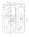
- FIG. 2is a block diagram of an example controller of the power inverter of FIG. 1 .
- FIG. 5is a circuit diagram another example portion of the power inverter of FIG. 1 .
- FIG. 6is a circuit diagram another example portion of the power inverter of FIG. 1 .
- FIG. 7is one example of an operational flow diagram of the power inverter of FIG. 1 .
- the inverter 100may include an input bridge (IB) 110 .
- the input bridge 110may include one or more circuit elements coupled to one another to convert the DC power from the DC power supply 102 to AC power.
- One example of the input bridge 110is shown in FIG. 4 .
- a line inductance (L l ) 112 coupled between the power supply 102 and the input bridge 110is represented by an inductive element.
- the line inductance 112may be one or more inductors used to reduce the current ripple transmitted to the DC power supply 102 .
- the input bridge 110may be coupled to a transformer 114 having a primary side 115 and secondary side 117 .
- the primary side 115 of the transformermay include a first winding 116 and the secondary side 117 may include a second winding 118 .
- Each of the first winding 116 and the second winding 118may include more than one winding coupled in series or other configuration.
- the transformer 114may have a winding ratio of 1:N to step up or step down the voltage and current from the output of the input bridge 110 .
- a rectifier (RECT) 119may be coupled to the second winding 118 of the transformer 114 .
- the inverter 100may include a line filter 123 to filter output voltage of the output bridge 122 prior to the AC power being delivered to the output load 108 .
- a line filter 123is shown in FIG. 6 .
- the output load 108may be a residential AC load having a split-phase configuration such as that found at residential premises in a United States electrical grid. In other examples, the output load 108 may be an industrial premises or any other load configured to receive AC power.
- the inverter 100may also be grounded on the DC side of the output bridge 122 , or alternatively on the AC side of the output bridge 122 , as shown by ground connections 128 and 130 , respectively.
- the groundingsmay be connected to other locations on the inverter 100 on the primary side 115 and/or the secondary side 117 of the inverter 100 .
- knowledge of the operating conditions of the power supply 102may be desired, such as the instantaneous voltage V DC and current I DC . While these conditions may be monitored on the primary side 115 of the transformer 114 , due to the isolation barrier in the inverter 100 , no common physical connections are present connecting both the primary side 115 and secondary side 117 for monitoring. However, knowledge of the operating conditions on the primary side 115 of the transformer 114 may be desired to be available on the secondary side 117 of the transformer 114 in order to control power being delivered to the output load 108 or for informational purposes.
- the inverter 100may include a primary side controller (PSC) 132 and a secondary side controller (SSC) 134 .
- the primary side controller 132may determine the operating conditions (e.g., current, voltage, impedance, capacitance, other characteristics, or combinations thereof) from the power supply 102 , such as the voltage V DC , from a sensor 133 .
- the sensor 133may be a voltage divider circuit or other circuit configured to sense the voltage produced by the power source 102 .
- An input sense resistor (R si ) 135may be used to provide the current I DC , or a current representative of I DC to the primary side controller 132 .
- the primary side controller 132may generate one or more control signals 136 to control the output of the input bridge 114 , as explained in further detail in FIG. 2 .
- the input bridge 110may be controlled to generate an output voltage v ib having a series of pulses alternating in polarity supplied to the first winding 116 of the transformer 114 .
- Supplying the output voltage v ib to the first winding 116may cause a primary voltage v pri to be applied across the first winding 116 .
- Current flowing from the input bridge 110 (see FIG. 4 ) into the first winding 116may cause the first winding 116 to experience a change in magnetic flux resulting in a secondary voltage v sec being created in the second winding 118 on the secondary side 117 of the transformer 114 .
- the control signals 136 generated by the primary side controller 132may control the duty cycle d (pulse width) and/or the frequency f p of the pulses of the output voltage v ib .
- the input bridge 110may be controlled by the primary side controller 132 to produce a voltage including pulses at a desired frequency f p .
- the frequency of the primary side voltage v primay have a frequency of f p resulting in the secondary side voltage v sec having a frequency of f p as well.
- the frequency f pmay be varied within a particular range without any significant adverse effects regarding the desired output of the inverter 100 .
- Varying the frequency f pmay allow information regarding the operating conditions of the power supply 102 to be conveyed to the secondary side 117 of the transformer 114 without physical connection to the primary side 115 of the transformer 114 or without the need to implement other manners of communication between the primary side 115 and the secondary side 117 , such as wireless communication (e.g., light emitting diodes, radio frequency transmission, capacitive coupling, etc.) between the primary side controller 132 and the secondary side controller 134 .
- wireless communicatione.g., light emitting diodes, radio frequency transmission, capacitive coupling, etc.
- the secondary side controller 134may detect the secondary voltage v sec across the second winding 118 through one or more sensors 140 , such as voltage divider circuit, for example.
- the secondary voltage v secmay be received by a rectifier 142 .
- the secondary voltage v secmay be buffered and scaled by a scaling device 143 , such as an op amp, comparator, or other suitable device, in order to be compatible with logic-level integrated circuits.
- the output voltage v ro of the rectifier 142may be a unipolar pulse train with a frequency double that of the voltage v sec ⁇ frequency f p .
- the secondary side controller 134may determine the operating conditions of the power supply 102 based on the output voltage v ro as further described with regard to FIG. 3 .
- a communication device 146may be used to transmit the operating conditions wirelessly, such as to a central authority for processing and analysis. In other examples, operating conditions of the DC power supply may be communicated through power lines electrically coupled to the output load 108 as an alternative to the communication device 146 or used in tandem.
- FIG. 2is a block diagram of an example of the primary side controller 132 .
- the primary side controller 132may be a microcontroller including a processor 200 , a memory 202 , clock 203 , and I/O ports.
- the memory 202may include one or more memories and may be non-transitory computer-readable storage media or memories, such as a cache, buffer, RAM, removable media, hard drive or other computer readable storage media.
- Computer readable storage mediamay include various types of volatile and nonvolatile storage media.
- Various processing techniquesmay be implemented by the processor 200 such as multiprocessing, multitasking, parallel processing and the like, for example.
- the processor 200may include one or more processors.
- the periodic update signal 219may indicate to the read module 210 the time at which the read module 210 may sample the data signals 206 .
- the periodic update signal 219may be generated at a predetermined update period of T update .
- the update period T updatemay be dynamically adjusted during operation of the inverter 100 .
- the read module 210may provide the data 206 to an encoding module (EM) 214 .
- the encoding module 214may retrieve encoding data 216 from the memory 202 .
- the encoding data 216may indicate a particular frequency at which to control the frequency f p of output voltage V ib in order to convey the operating conditions of the power supply 102 to the secondary side 117 of the transformer 114 .
- the encoding data 216may include one or more tables mapping particular frequency values to particular operating condition points of the power supply 15 102 . Table 1 below is one example of the encoding data 216 in which the desired operating frequency range of the input bridge 110 has a midpoint of approximately 50 kHz.
- the frequency f pmay be modulated within a range of about +/ ⁇ 5% of a particular switching frequency, however, in order to convey operating condition information regarding the power supply 102 to the secondary side 117 of the transformer 114 .
- Other tolerancesare possible.
- the decoding data 318may include tables having a number of possible operating conditions points of the power supply 102 . Each possible operating condition points in the table may correspond to a particular number of pulses counted by the pulse counter over the period of T read .
Landscapes
- Engineering & Computer Science (AREA)
- Power Engineering (AREA)
- Inverter Devices (AREA)
- Dc-Dc Converters (AREA)
Abstract
Description
| TABLE 1 | ||||||
| Current/ | ||||||
| Voltage | 0 A | 0.5 A | 1.0 A | 1.5 A | . . . | 10 A |
| 0 V | 49,500 Hz | 49,550.5 Hz | 49,551 Hz | 49,551.5 Hz | . . . | 49,509.5 Hz |
| 0.5 V | 49,510 Hz | 49,510.5 Hz | 49,511 Hz | 49,511.5 Hz | . . . | 49,519.5 Hz |
| 1.0 V | 49,520 Hz | 49,520.5 Hz | 49,521 Hz | 49,521.5 Hz | . . . | 49,529.5 Hz |
| . . . | . . . | . . . | . . . | . . . | . . . | . . . |
| 50.0 V | 50,490 Hz | 50,490.5 Hz | 50,491 Hz | 50,491.5 Hz | . . . | 50,499.5 Hz |
| TABLE 2 | ||||||
| Voltage/Current | 0 A | 0.5 A | 1.0 A | 1.5 A | . . . | 10 A |
| 0 V | 99000 | 99001 | 99002 | 99003 | . . . | 99019 |
| 0.5 V | 99020 | 99021 | 99022 | 99023 | . . . | 99039 |
| 1.0 V | 99040 | 99041 | 99042 | 99043 | . . . | 99059 |
| . . . | . . . | . . . | . . . | . . . | . . . | . . . |
| 50.0 V | 100980 | 100981 | 100982 | 100983 | . . . | 100999 |
Table 2 may be applied to the situation in which the voltage produced of the
Claims (23)
Priority Applications (4)
| Application Number | Priority Date | Filing Date | Title |
|---|---|---|---|
| US12/832,199US8634216B2 (en) | 2010-07-08 | 2010-07-08 | Communication within a power inverter using transformer voltage frequency |
| PCT/US2011/042190WO2012006092A2 (en) | 2010-07-08 | 2011-06-28 | Communication within a power inverter using transformer voltage frequency |
| US14/159,084US9509232B2 (en) | 2010-07-08 | 2014-01-20 | Communication within a power inverter using transformer voltage frequency |
| US15/355,843US9887639B2 (en) | 2010-07-08 | 2016-11-18 | Communication within a power inverter using transformer voltage frequency |
Applications Claiming Priority (1)
| Application Number | Priority Date | Filing Date | Title |
|---|---|---|---|
| US12/832,199US8634216B2 (en) | 2010-07-08 | 2010-07-08 | Communication within a power inverter using transformer voltage frequency |
Related Child Applications (1)
| Application Number | Title | Priority Date | Filing Date |
|---|---|---|---|
| US14/159,084ContinuationUS9509232B2 (en) | 2010-07-08 | 2014-01-20 | Communication within a power inverter using transformer voltage frequency |
Publications (2)
| Publication Number | Publication Date |
|---|---|
| US20120008348A1 US20120008348A1 (en) | 2012-01-12 |
| US8634216B2true US8634216B2 (en) | 2014-01-21 |
Family
ID=45438445
Family Applications (3)
| Application Number | Title | Priority Date | Filing Date |
|---|---|---|---|
| US12/832,199Active2032-04-04US8634216B2 (en) | 2010-07-08 | 2010-07-08 | Communication within a power inverter using transformer voltage frequency |
| US14/159,084Expired - Fee RelatedUS9509232B2 (en) | 2010-07-08 | 2014-01-20 | Communication within a power inverter using transformer voltage frequency |
| US15/355,843ActiveUS9887639B2 (en) | 2010-07-08 | 2016-11-18 | Communication within a power inverter using transformer voltage frequency |
Family Applications After (2)
| Application Number | Title | Priority Date | Filing Date |
|---|---|---|---|
| US14/159,084Expired - Fee RelatedUS9509232B2 (en) | 2010-07-08 | 2014-01-20 | Communication within a power inverter using transformer voltage frequency |
| US15/355,843ActiveUS9887639B2 (en) | 2010-07-08 | 2016-11-18 | Communication within a power inverter using transformer voltage frequency |
Country Status (2)
| Country | Link |
|---|---|
| US (3) | US8634216B2 (en) |
| WO (1) | WO2012006092A2 (en) |
Cited By (18)
| Publication number | Priority date | Publication date | Assignee | Title |
|---|---|---|---|---|
| WO2016079910A1 (en)* | 2014-11-21 | 2016-05-26 | 公立大学法人大阪市立大学 | Drive control device and drive control system comprising same |
| US20160181861A1 (en)* | 2014-12-19 | 2016-06-23 | Eaton Corporation | Power systems and methods using voltage waveform signaling |
| US20170373606A1 (en)* | 2016-06-24 | 2017-12-28 | Semiconductor Components Industries, Llc | Communication circuit for flyback power converter with synchronous rectifier |
| USD822890S1 (en) | 2016-09-07 | 2018-07-10 | Felxtronics Ap, Llc | Lighting apparatus |
| USD832494S1 (en) | 2017-08-09 | 2018-10-30 | Flex Ltd. | Lighting module heatsink |
| USD832495S1 (en) | 2017-08-18 | 2018-10-30 | Flex Ltd. | Lighting module locking mechanism |
| USD833061S1 (en) | 2017-08-09 | 2018-11-06 | Flex Ltd. | Lighting module locking endcap |
| US20180351504A1 (en)* | 2017-06-02 | 2018-12-06 | Sunpower Corporation | Hybrid management module |
| USD846793S1 (en) | 2017-08-09 | 2019-04-23 | Flex Ltd. | Lighting module locking mechanism |
| US10277278B2 (en) | 2014-09-24 | 2019-04-30 | Analog Devices, Inc. | Circuits and systems for multiplexed isolator communication |
| USD862777S1 (en) | 2017-08-09 | 2019-10-08 | Flex Ltd. | Lighting module wide distribution lens |
| USD862778S1 (en) | 2017-08-22 | 2019-10-08 | Flex Ltd | Lighting module lens |
| USD872319S1 (en) | 2017-08-09 | 2020-01-07 | Flex Ltd. | Lighting module LED light board |
| USD877964S1 (en) | 2017-08-09 | 2020-03-10 | Flex Ltd. | Lighting module |
| USD888323S1 (en) | 2017-09-07 | 2020-06-23 | Flex Ltd | Lighting module wire guard |
| US10775030B2 (en) | 2017-05-05 | 2020-09-15 | Flex Ltd. | Light fixture device including rotatable light modules |
| US10924018B2 (en)* | 2013-05-01 | 2021-02-16 | Texas Instruments Incorporated | Tracking energy consumption using a boost-buck technique |
| US11791633B2 (en) | 2011-07-11 | 2023-10-17 | Generac Power Systems, Inc. | Systems and methods for increasing output current quality, output power, and reliability of grid-interactive inverters |
Families Citing this family (14)
| Publication number | Priority date | Publication date | Assignee | Title |
|---|---|---|---|---|
| EP2637293B1 (en)* | 2012-03-07 | 2018-08-01 | Dialog Semiconductor GmbH | Active rectifier with modulation |
| WO2013146017A1 (en)* | 2012-03-26 | 2013-10-03 | 株式会社村田製作所 | Power transmitting system, and power transmitting apparatus used tehrein |
| US9647571B2 (en) | 2013-08-02 | 2017-05-09 | Solantro Semiconductor Corp. | Internal inverter communications |
| US9973099B2 (en)* | 2015-08-26 | 2018-05-15 | Futurewei Technologies, Inc. | AC/DC converters with wider voltage regulation range |
| JP6299779B2 (en)* | 2016-02-02 | 2018-03-28 | トヨタ自動車株式会社 | Power transmission device and power transmission system |
| CN107046370B (en)* | 2016-02-09 | 2020-05-26 | 松下知识产权经营株式会社 | Converter, power transmission system and controller |
| US11387743B2 (en)* | 2017-07-20 | 2022-07-12 | Panasonic Intellectual Property Management Co., Ltd. | Power supply device and control method for stably operating a device when a frequency of an input power supply fluctuates |
| CN110350602A (en)* | 2018-04-03 | 2019-10-18 | 中国电力科学研究院有限公司 | Participate in the blower fan control system of power grid frequency modulation |
| CN109194115A (en)* | 2018-08-29 | 2019-01-11 | 合肥德铭电子有限公司 | Cavity mirror system electromagnetism suppressing device and cavity mirror system |
| US10951107B2 (en)* | 2019-06-27 | 2021-03-16 | Cypress Semiconductor Corporation | Communicating fault indications between primary and secondary controllers in a secondary-controlled flyback converter |
| US11183939B2 (en)* | 2020-02-18 | 2021-11-23 | Infineon Technologies Austria Ag | Reliable communication through a flyback power transformer using a zero voltage switching pulse |
| CN114172381B (en)* | 2022-02-11 | 2022-04-15 | 四川大学 | A capacitor energy storage type isolated DC-DC converter and its control method |
| CN116054594B (en)* | 2023-04-01 | 2023-06-23 | 苏州美思迪赛半导体技术有限公司 | A Switching Power Supply System with Simultaneous Analog Feedback and Digital Feedback |
| CN116054593B (en)* | 2023-04-01 | 2023-06-13 | 苏州美思迪赛半导体技术有限公司 | A method for switching power supply to transmit information through transformer |
Citations (15)
| Publication number | Priority date | Publication date | Assignee | Title |
|---|---|---|---|---|
| US5436820A (en)* | 1993-06-09 | 1995-07-25 | Eldec Corporation | Power converter with dual PWM control |
| US5625539A (en)* | 1994-05-30 | 1997-04-29 | Sharp Kabushiki Kaisha | Method and apparatus for controlling a DC to AC inverter system by a plurality of pulse-width modulated pulse trains |
| US5719758A (en)* | 1995-12-20 | 1998-02-17 | Sharp Kabushiki Kaisha | Inverter control method and inverter apparatus using the method |
| US6339538B1 (en) | 1998-06-22 | 2002-01-15 | Clayton Kling Philips Handleman | Inverter circuit and method of operation |
| US20020154526A1 (en)* | 2001-04-18 | 2002-10-24 | Keijirou Sakai | PWM converter system |
| US6563718B1 (en)* | 2001-12-06 | 2003-05-13 | Koninklijke Philips Electronics N.V. | Capacitively coupled power converter |
| US6602627B2 (en) | 2000-03-20 | 2003-08-05 | Alpha Technologies, Inc. | Uninterruptible power supplies using fuel cells |
| US6704213B2 (en) | 2000-12-18 | 2004-03-09 | Abb Schweiz Ag | Voltage converter system having a plurality of voltage inverters for increasing a DC voltage |
| US6909620B2 (en) | 2003-04-25 | 2005-06-21 | Wisconsin Alumni Research Foundation | Inverter configurations with shoot-through immunity |
| US6934167B2 (en)* | 2003-05-01 | 2005-08-23 | Delta Electronics, Inc. | Contactless electrical energy transmission system having a primary side current feedback control and soft-switched secondary side rectifier |
| US20060221653A1 (en)* | 2003-11-25 | 2006-10-05 | Jih-Sheng Lai | Multilevel converter based intelligent universal transformer |
| US20060256598A1 (en) | 2005-05-10 | 2006-11-16 | Kwok-Pun Ho | Inverter device |
| US20070042729A1 (en)* | 2005-08-16 | 2007-02-22 | Baaman David W | Inductive power supply, remote device powered by inductive power supply and method for operating same |
| US20080096068A1 (en) | 2006-10-24 | 2008-04-24 | Toyota Jidosha Kabushiki Kaisha | Fuel cell system |
| US20090251933A1 (en)* | 2006-09-04 | 2009-10-08 | Christian Angerer | Method for controlling inverters |
Family Cites Families (1)
| Publication number | Priority date | Publication date | Assignee | Title |
|---|---|---|---|---|
| TWI340528B (en)* | 2007-04-03 | 2011-04-11 | Delta Electronics Inc | Resonant converter system and controlling method thereof having relatively better efficiency |
- 2010
- 2010-07-08USUS12/832,199patent/US8634216B2/enactiveActive
- 2011
- 2011-06-28WOPCT/US2011/042190patent/WO2012006092A2/enactiveApplication Filing
- 2014
- 2014-01-20USUS14/159,084patent/US9509232B2/ennot_activeExpired - Fee Related
- 2016
- 2016-11-18USUS15/355,843patent/US9887639B2/enactiveActive
Patent Citations (15)
| Publication number | Priority date | Publication date | Assignee | Title |
|---|---|---|---|---|
| US5436820A (en)* | 1993-06-09 | 1995-07-25 | Eldec Corporation | Power converter with dual PWM control |
| US5625539A (en)* | 1994-05-30 | 1997-04-29 | Sharp Kabushiki Kaisha | Method and apparatus for controlling a DC to AC inverter system by a plurality of pulse-width modulated pulse trains |
| US5719758A (en)* | 1995-12-20 | 1998-02-17 | Sharp Kabushiki Kaisha | Inverter control method and inverter apparatus using the method |
| US6339538B1 (en) | 1998-06-22 | 2002-01-15 | Clayton Kling Philips Handleman | Inverter circuit and method of operation |
| US6602627B2 (en) | 2000-03-20 | 2003-08-05 | Alpha Technologies, Inc. | Uninterruptible power supplies using fuel cells |
| US6704213B2 (en) | 2000-12-18 | 2004-03-09 | Abb Schweiz Ag | Voltage converter system having a plurality of voltage inverters for increasing a DC voltage |
| US20020154526A1 (en)* | 2001-04-18 | 2002-10-24 | Keijirou Sakai | PWM converter system |
| US6563718B1 (en)* | 2001-12-06 | 2003-05-13 | Koninklijke Philips Electronics N.V. | Capacitively coupled power converter |
| US6909620B2 (en) | 2003-04-25 | 2005-06-21 | Wisconsin Alumni Research Foundation | Inverter configurations with shoot-through immunity |
| US6934167B2 (en)* | 2003-05-01 | 2005-08-23 | Delta Electronics, Inc. | Contactless electrical energy transmission system having a primary side current feedback control and soft-switched secondary side rectifier |
| US20060221653A1 (en)* | 2003-11-25 | 2006-10-05 | Jih-Sheng Lai | Multilevel converter based intelligent universal transformer |
| US20060256598A1 (en) | 2005-05-10 | 2006-11-16 | Kwok-Pun Ho | Inverter device |
| US20070042729A1 (en)* | 2005-08-16 | 2007-02-22 | Baaman David W | Inductive power supply, remote device powered by inductive power supply and method for operating same |
| US20090251933A1 (en)* | 2006-09-04 | 2009-10-08 | Christian Angerer | Method for controlling inverters |
| US20080096068A1 (en) | 2006-10-24 | 2008-04-24 | Toyota Jidosha Kabushiki Kaisha | Fuel cell system |
Non-Patent Citations (9)
| Title |
|---|
| Chen, R.Y. et al, Current-fed Full-bridge Boost Converter with Zero Current Switching for High Voltage Applications, IAS 2005, 0-7803-9208-6/05/$20.00 c 2005 IEEE, pp. 2000-2006, Power Electronics Laboratory, Department of Electrical Engineering, National Cheng-Kung University, Tainan City, Taiwan, R.O.C. |
| International Search Report and Written Opinion, PCT/US2011/042190, Feb. 9, 2012. |
| Lai, R-S., et al, A PWM Method for Reduction of Switching Loss in a Full-Bridge Inverter, IEEE Transactions on Power Electronics, vol. 10, No. 3, May 1995, pp. 326-332. |
| Liu, J., et al, A Novel Three Level Dual Buck Half Bridge Inverter, 978-1-4244-1874-9/08/$25.00 c2008 IEEE, pp. 483-487. |
| Wang, Z., et al, Simulation Study of Charge Controlled Half-cycle Modulated Dual Buck Half Bridge Inverter, Nanjing University of Aero.& Astro., College of Automation, Nanjing, China. |
| Yao, Z., et al, A Novel Control Strategy for Grid-Interactive Inverter in Grid-Connected and Stand-Alone Modes* (*This work was supported by the National Natural Science Foundation of China (50337030) and delta foundation.), 0-7803-9547-6/06/$20.00 c2006 IEEE., pp. 779-783, Aero-Power Sci-tech Center, College of Automation Engineering, Nanjing University of Aeronautics and Astronautics, Nanjing, P.R. China. |
| Yao, Z., Two-Switch Dual-Buck Grid-Connected Inverter, 978-1-4244-3557-9/09/$25.00 c2009 IEEE, pp. 2182-2187, College of Electrical Engineering, Yancheng Institute of Technology, Yancheng, China. |
| Yu, H., et al, A Novel Load Adaptive Zero Voltage Switching Utilizing Diode Reverse Recovery current for Soft-Switching Choppers and Inverters, 0-7803-7067-8/01/$10.00 c2001 IEEE, pp. 146-151, Center for Power Electronics Systems, The Bradley Department of Electrical and Computer Engineering, Virginia Polytechnic Institute and State University, Blacksburg, VA, USA. |
| Zhu, C., et al, A Novel Split Phase Dual Buck Half Bridge Inverter, 0-7803-8975-1/05/$20.00 c2005 IEEE, pp. 845-849, Aero-Power Sci-Tech Center, Nanjing University of Aeronautics & Astronautics, Nanjing, P.R. China. |
Cited By (35)
| Publication number | Priority date | Publication date | Assignee | Title |
|---|---|---|---|---|
| US12176719B2 (en) | 2011-07-11 | 2024-12-24 | Generac Power Systems, Inc. | Systems and methods for increasing output current quality, output power, and reliability of grid-interactive inverters |
| US11791633B2 (en) | 2011-07-11 | 2023-10-17 | Generac Power Systems, Inc. | Systems and methods for increasing output current quality, output power, and reliability of grid-interactive inverters |
| US10924018B2 (en)* | 2013-05-01 | 2021-02-16 | Texas Instruments Incorporated | Tracking energy consumption using a boost-buck technique |
| US11398848B2 (en) | 2014-09-24 | 2022-07-26 | Analog Devices, Inc. | Circuits and systems for multiplexed isolator communication |
| US10277278B2 (en) | 2014-09-24 | 2019-04-30 | Analog Devices, Inc. | Circuits and systems for multiplexed isolator communication |
| US10411758B2 (en)* | 2014-11-21 | 2019-09-10 | Osaka City University | Drive control apparatus that receives power and a plurality of frequency-multiplexed control signals |
| JPWO2016079910A1 (en)* | 2014-11-21 | 2017-08-31 | 公立大学法人大阪市立大学 | Drive control device and drive control system having the same |
| US20170324445A1 (en)* | 2014-11-21 | 2017-11-09 | Osaka City University | Drive control device and drive control system comprising same |
| WO2016079910A1 (en)* | 2014-11-21 | 2016-05-26 | 公立大学法人大阪市立大学 | Drive control device and drive control system comprising same |
| US11159042B2 (en) | 2014-12-19 | 2021-10-26 | Eaton Intelligent Power Limited | Power systems and methods using voltage waveform signaling |
| US10447072B2 (en)* | 2014-12-19 | 2019-10-15 | Eaton Intelligent Power Limited | Power systems and methods using voltage waveform signaling |
| US20160181861A1 (en)* | 2014-12-19 | 2016-06-23 | Eaton Corporation | Power systems and methods using voltage waveform signaling |
| US10158298B2 (en)* | 2016-06-24 | 2018-12-18 | Semiconductor Components Industries, Llc | Communication circuit for flyback power converter with synchronous rectifier |
| US9985548B2 (en)* | 2016-06-24 | 2018-05-29 | Semiconductor Components Industries, Llc | Communication circuit for flyback power converter with synchronous rectifier |
| US20170373606A1 (en)* | 2016-06-24 | 2017-12-28 | Semiconductor Components Industries, Llc | Communication circuit for flyback power converter with synchronous rectifier |
| USD822890S1 (en) | 2016-09-07 | 2018-07-10 | Felxtronics Ap, Llc | Lighting apparatus |
| US10775030B2 (en) | 2017-05-05 | 2020-09-15 | Flex Ltd. | Light fixture device including rotatable light modules |
| US20180351504A1 (en)* | 2017-06-02 | 2018-12-06 | Sunpower Corporation | Hybrid management module |
| US10886874B2 (en)* | 2017-06-02 | 2021-01-05 | Sunpower Corporation | Hybrid management module |
| USD885615S1 (en) | 2017-08-09 | 2020-05-26 | Flex Ltd. | Lighting module LED light board |
| USD853625S1 (en) | 2017-08-09 | 2019-07-09 | Flex Ltd | Lighting module heatsink |
| USD862777S1 (en) | 2017-08-09 | 2019-10-08 | Flex Ltd. | Lighting module wide distribution lens |
| USD872319S1 (en) | 2017-08-09 | 2020-01-07 | Flex Ltd. | Lighting module LED light board |
| USD877964S1 (en) | 2017-08-09 | 2020-03-10 | Flex Ltd. | Lighting module |
| USD853627S1 (en) | 2017-08-09 | 2019-07-09 | Flex Ltd | Lighting module locking endcap |
| USD832494S1 (en) | 2017-08-09 | 2018-10-30 | Flex Ltd. | Lighting module heatsink |
| USD1010915S1 (en) | 2017-08-09 | 2024-01-09 | Linmore Labs Led, Inc. | Lighting module |
| USD905325S1 (en) | 2017-08-09 | 2020-12-15 | Flex Ltd | Lighting module |
| USD853629S1 (en) | 2017-08-09 | 2019-07-09 | Flex Ltd | Lighting module locking mechanism |
| USD833061S1 (en) | 2017-08-09 | 2018-11-06 | Flex Ltd. | Lighting module locking endcap |
| USD846793S1 (en) | 2017-08-09 | 2019-04-23 | Flex Ltd. | Lighting module locking mechanism |
| USD853628S1 (en) | 2017-08-18 | 2019-07-09 | Flex Ltd. | Lighting module locking mechanism |
| USD832495S1 (en) | 2017-08-18 | 2018-10-30 | Flex Ltd. | Lighting module locking mechanism |
| USD862778S1 (en) | 2017-08-22 | 2019-10-08 | Flex Ltd | Lighting module lens |
| USD888323S1 (en) | 2017-09-07 | 2020-06-23 | Flex Ltd | Lighting module wire guard |
Also Published As
| Publication number | Publication date |
|---|---|
| US20120008348A1 (en) | 2012-01-12 |
| WO2012006092A3 (en) | 2012-04-05 |
| US20140133197A1 (en) | 2014-05-15 |
| US9509232B2 (en) | 2016-11-29 |
| US9887639B2 (en) | 2018-02-06 |
| US20170070156A1 (en) | 2017-03-09 |
| WO2012006092A2 (en) | 2012-01-12 |
Similar Documents
| Publication | Publication Date | Title |
|---|---|---|
| US8634216B2 (en) | Communication within a power inverter using transformer voltage frequency | |
| US9001543B2 (en) | Active rectifier with modulation | |
| CN205092774U (en) | Power supply circuit , relevant transmitting circuit , integrated circuit | |
| US9860947B2 (en) | Driver circuit for illuminants, particularly LEDs | |
| TWI835066B (en) | Series resonant llc converter and method of operating a series resonant llc converter | |
| CN111049385B (en) | System for communication, and apparatus and method for detection | |
| AU2014355917B2 (en) | Power source apparatus and electric device | |
| KR101278850B1 (en) | Power converter circuit | |
| US10148128B2 (en) | Power-supplying device, and wireless power-supplying system | |
| CN109713918A (en) | With PFC without bridge AC-DC converter and its method | |
| JP2008533960A (en) | Switched mode power conversion device and operation method thereof | |
| CN107078644B (en) | Operation circuit, the operating method of LED converter and operation circuit powered to lighting means | |
| KR101594699B1 (en) | AC Power Line Communication System | |
| CN104953682A (en) | Circuit with wireless charging transmitting function and wireless charging receiving function and device thereof | |
| CN104796015A (en) | System and method for supplying a synchronous rectifier driver circuit | |
| TWI489759B (en) | Power conversion system and method | |
| US9564819B2 (en) | Switching power supply circuit | |
| EP3008978A1 (en) | Led lighting converter | |
| US8891263B2 (en) | Inverter apparatus having power supply circuit | |
| US8582318B2 (en) | Circuit and method for potential-isolated energy transfer with two output DC voltages | |
| KR20210014520A (en) | Buck boost converter and wireless power transmission device including the same | |
| JP2017005841A (en) | Power transmission apparatus | |
| JP2007124759A (en) | Dc converter | |
| KR20250120848A (en) | Power conversion device | |
| WO2013115751A1 (en) | Voltage converter |
Legal Events
| Date | Code | Title | Description |
|---|---|---|---|
| AS | Assignment | Owner name:SOLARBRIDGE TECHNOLOGIES, ILLINOIS Free format text:ASSIGNMENT OF ASSIGNORS INTEREST;ASSIGNOR:CHAPMAN, PATRICK L.;REEL/FRAME:024665/0994 Effective date:20100707 | |
| AS | Assignment | Owner name:SOLARBRIDGE TECHNOLOGIES, INC., TEXAS Free format text:CORRECTIVE ASSIGNMENT TO CORRECT REEL/FRAME 024665/0994 ASSIGNEE NAME;ASSIGNOR:CHAPMAN, PATRICK L.;REEL/FRAME:026847/0941 Effective date:20110725 | |
| STCF | Information on status: patent grant | Free format text:PATENTED CASE | |
| AS | Assignment | Owner name:SILICON VALLEY BANK, CALIFORNIA Free format text:SECURITY INTEREST;ASSIGNOR:SOLARBRIDGE TECHNOLOGIES, INC.;REEL/FRAME:033677/0870 Effective date:20130724 | |
| FEPP | Fee payment procedure | Free format text:PAT HOLDER NO LONGER CLAIMS SMALL ENTITY STATUS, ENTITY STATUS SET TO UNDISCOUNTED (ORIGINAL EVENT CODE: STOL); ENTITY STATUS OF PATENT OWNER: LARGE ENTITY | |
| AS | Assignment | Owner name:SUNPOWER CORPORATION, CALIFORNIA Free format text:ASSIGNMENT OF ASSIGNORS INTEREST;ASSIGNOR:SOLARBRIDGE TECHNOLOGIES, INC.;REEL/FRAME:034687/0232 Effective date:20141218 Owner name:SOLARBRIDGE TECHNOLOGIES, INC., TEXAS Free format text:RELEASE BY SECURED PARTY;ASSIGNOR:SILICON VALLEY BANK;REEL/FRAME:034681/0475 Effective date:20141107 | |
| FPAY | Fee payment | Year of fee payment:4 | |
| AS | Assignment | Owner name:ENPHASE ENERGY, INC., CALIFORNIA Free format text:ASSIGNMENT OF ASSIGNORS INTEREST;ASSIGNOR:SUNPOWER CORPORATION;REEL/FRAME:046964/0203 Effective date:20180809 | |
| MAFP | Maintenance fee payment | Free format text:PAYMENT OF MAINTENANCE FEE, 8TH YEAR, LARGE ENTITY (ORIGINAL EVENT CODE: M1552); ENTITY STATUS OF PATENT OWNER: LARGE ENTITY Year of fee payment:8 | |
| MAFP | Maintenance fee payment | Free format text:PAYMENT OF MAINTENANCE FEE, 12TH YEAR, LARGE ENTITY (ORIGINAL EVENT CODE: M1553); ENTITY STATUS OF PATENT OWNER: LARGE ENTITY Year of fee payment:12 |