US8633112B2 - Thermal anneal of block copolymer films with top interface constrained to wet both blocks with equal preference - Google Patents
Thermal anneal of block copolymer films with top interface constrained to wet both blocks with equal preferenceDownload PDFInfo
- Publication number
- US8633112B2 US8633112B2US13/469,697US201213469697AUS8633112B2US 8633112 B2US8633112 B2US 8633112B2US 201213469697 AUS201213469697 AUS 201213469697AUS 8633112 B2US8633112 B2US 8633112B2
- Authority
- US
- United States
- Prior art keywords
- block copolymer
- copolymer material
- poly
- self
- block
- Prior art date
- Legal status (The legal status is an assumption and is not a legal conclusion. Google has not performed a legal analysis and makes no representation as to the accuracy of the status listed.)
- Active
Links
Images


Classifications
- H—ELECTRICITY
- H01—ELECTRIC ELEMENTS
- H01L—SEMICONDUCTOR DEVICES NOT COVERED BY CLASS H10
- H01L21/00—Processes or apparatus adapted for the manufacture or treatment of semiconductor or solid state devices or of parts thereof
- H01L21/70—Manufacture or treatment of devices consisting of a plurality of solid state components formed in or on a common substrate or of parts thereof; Manufacture of integrated circuit devices or of parts thereof
- H01L21/71—Manufacture of specific parts of devices defined in group H01L21/70
- H01L21/768—Applying interconnections to be used for carrying current between separate components within a device comprising conductors and dielectrics
- H01L21/76801—Applying interconnections to be used for carrying current between separate components within a device comprising conductors and dielectrics characterised by the formation and the after-treatment of the dielectrics, e.g. smoothing
- H01L21/76822—Modification of the material of dielectric layers, e.g. grading, after-treatment to improve the stability of the layers, to increase their density etc.
- H01L21/76828—Modification of the material of dielectric layers, e.g. grading, after-treatment to improve the stability of the layers, to increase their density etc. thermal treatment
- B—PERFORMING OPERATIONS; TRANSPORTING
- B81—MICROSTRUCTURAL TECHNOLOGY
- B81C—PROCESSES OR APPARATUS SPECIALLY ADAPTED FOR THE MANUFACTURE OR TREATMENT OF MICROSTRUCTURAL DEVICES OR SYSTEMS
- B81C1/00—Manufacture or treatment of devices or systems in or on a substrate
- B81C1/00015—Manufacture or treatment of devices or systems in or on a substrate for manufacturing microsystems
- B81C1/00023—Manufacture or treatment of devices or systems in or on a substrate for manufacturing microsystems without movable or flexible elements
- B81C1/00031—Regular or irregular arrays of nanoscale structures, e.g. etch mask layer
- B—PERFORMING OPERATIONS; TRANSPORTING
- B82—NANOTECHNOLOGY
- B82Y—SPECIFIC USES OR APPLICATIONS OF NANOSTRUCTURES; MEASUREMENT OR ANALYSIS OF NANOSTRUCTURES; MANUFACTURE OR TREATMENT OF NANOSTRUCTURES
- B82Y30/00—Nanotechnology for materials or surface science, e.g. nanocomposites
- C—CHEMISTRY; METALLURGY
- C08—ORGANIC MACROMOLECULAR COMPOUNDS; THEIR PREPARATION OR CHEMICAL WORKING-UP; COMPOSITIONS BASED THEREON
- C08F—MACROMOLECULAR COMPOUNDS OBTAINED BY REACTIONS ONLY INVOLVING CARBON-TO-CARBON UNSATURATED BONDS
- C08F299/00—Macromolecular compounds obtained by interreacting polymers involving only carbon-to-carbon unsaturated bond reactions, in the absence of non-macromolecular monomers
- C08F299/02—Macromolecular compounds obtained by interreacting polymers involving only carbon-to-carbon unsaturated bond reactions, in the absence of non-macromolecular monomers from unsaturated polycondensates
- C08F299/04—Macromolecular compounds obtained by interreacting polymers involving only carbon-to-carbon unsaturated bond reactions, in the absence of non-macromolecular monomers from unsaturated polycondensates from polyesters
- C08F299/0485—Macromolecular compounds obtained by interreacting polymers involving only carbon-to-carbon unsaturated bond reactions, in the absence of non-macromolecular monomers from unsaturated polycondensates from polyesters from polyesters with side or terminal unsaturations
- C08F299/0492—Macromolecular compounds obtained by interreacting polymers involving only carbon-to-carbon unsaturated bond reactions, in the absence of non-macromolecular monomers from unsaturated polycondensates from polyesters from polyesters with side or terminal unsaturations the unsaturation being in acrylic or methacrylic groups
- G—PHYSICS
- G03—PHOTOGRAPHY; CINEMATOGRAPHY; ANALOGOUS TECHNIQUES USING WAVES OTHER THAN OPTICAL WAVES; ELECTROGRAPHY; HOLOGRAPHY
- G03F—PHOTOMECHANICAL PRODUCTION OF TEXTURED OR PATTERNED SURFACES, e.g. FOR PRINTING, FOR PROCESSING OF SEMICONDUCTOR DEVICES; MATERIALS THEREFOR; ORIGINALS THEREFOR; APPARATUS SPECIALLY ADAPTED THEREFOR
- G03F7/00—Photomechanical, e.g. photolithographic, production of textured or patterned surfaces, e.g. printing surfaces; Materials therefor, e.g. comprising photoresists; Apparatus specially adapted therefor
- G03F7/0002—Lithographic processes using patterning methods other than those involving the exposure to radiation, e.g. by stamping
- H—ELECTRICITY
- H01—ELECTRIC ELEMENTS
- H01L—SEMICONDUCTOR DEVICES NOT COVERED BY CLASS H10
- H01L21/00—Processes or apparatus adapted for the manufacture or treatment of semiconductor or solid state devices or of parts thereof
- H01L21/02—Manufacture or treatment of semiconductor devices or of parts thereof
- H01L21/027—Making masks on semiconductor bodies for further photolithographic processing not provided for in group H01L21/18 or H01L21/34
- H01L21/0271—Making masks on semiconductor bodies for further photolithographic processing not provided for in group H01L21/18 or H01L21/34 comprising organic layers
- H01L21/0273—Making masks on semiconductor bodies for further photolithographic processing not provided for in group H01L21/18 or H01L21/34 comprising organic layers characterised by the treatment of photoresist layers
- H01L21/0274—Photolithographic processes
- H01L21/0275—Photolithographic processes using lasers
- H—ELECTRICITY
- H01—ELECTRIC ELEMENTS
- H01L—SEMICONDUCTOR DEVICES NOT COVERED BY CLASS H10
- H01L21/00—Processes or apparatus adapted for the manufacture or treatment of semiconductor or solid state devices or of parts thereof
- H01L21/02—Manufacture or treatment of semiconductor devices or of parts thereof
- H01L21/027—Making masks on semiconductor bodies for further photolithographic processing not provided for in group H01L21/18 or H01L21/34
- H01L21/033—Making masks on semiconductor bodies for further photolithographic processing not provided for in group H01L21/18 or H01L21/34 comprising inorganic layers
- H01L21/0334—Making masks on semiconductor bodies for further photolithographic processing not provided for in group H01L21/18 or H01L21/34 comprising inorganic layers characterised by their size, orientation, disposition, behaviour, shape, in horizontal or vertical plane
- H01L21/0337—Making masks on semiconductor bodies for further photolithographic processing not provided for in group H01L21/18 or H01L21/34 comprising inorganic layers characterised by their size, orientation, disposition, behaviour, shape, in horizontal or vertical plane characterised by the process involved to create the mask, e.g. lift-off masks, sidewalls, or to modify the mask, e.g. pre-treatment, post-treatment
- H—ELECTRICITY
- H01—ELECTRIC ELEMENTS
- H01L—SEMICONDUCTOR DEVICES NOT COVERED BY CLASS H10
- H01L21/00—Processes or apparatus adapted for the manufacture or treatment of semiconductor or solid state devices or of parts thereof
- H01L21/02—Manufacture or treatment of semiconductor devices or of parts thereof
- H01L21/027—Making masks on semiconductor bodies for further photolithographic processing not provided for in group H01L21/18 or H01L21/34
- H01L21/033—Making masks on semiconductor bodies for further photolithographic processing not provided for in group H01L21/18 or H01L21/34 comprising inorganic layers
- H01L21/0334—Making masks on semiconductor bodies for further photolithographic processing not provided for in group H01L21/18 or H01L21/34 comprising inorganic layers characterised by their size, orientation, disposition, behaviour, shape, in horizontal or vertical plane
- H01L21/0338—Process specially adapted to improve the resolution of the mask
- H—ELECTRICITY
- H01—ELECTRIC ELEMENTS
- H01L—SEMICONDUCTOR DEVICES NOT COVERED BY CLASS H10
- H01L21/00—Processes or apparatus adapted for the manufacture or treatment of semiconductor or solid state devices or of parts thereof
- H01L21/02—Manufacture or treatment of semiconductor devices or of parts thereof
- H01L21/04—Manufacture or treatment of semiconductor devices or of parts thereof the devices having potential barriers, e.g. a PN junction, depletion layer or carrier concentration layer
- H01L21/18—Manufacture or treatment of semiconductor devices or of parts thereof the devices having potential barriers, e.g. a PN junction, depletion layer or carrier concentration layer the devices having semiconductor bodies comprising elements of Group IV of the Periodic Table or AIIIBV compounds with or without impurities, e.g. doping materials
- H01L21/30—Treatment of semiconductor bodies using processes or apparatus not provided for in groups H01L21/20 - H01L21/26
- H01L21/31—Treatment of semiconductor bodies using processes or apparatus not provided for in groups H01L21/20 - H01L21/26 to form insulating layers thereon, e.g. for masking or by using photolithographic techniques; After treatment of these layers; Selection of materials for these layers
- H01L21/3105—After-treatment
- H01L21/311—Etching the insulating layers by chemical or physical means
- H01L21/31127—Etching organic layers
- H01L21/31133—Etching organic layers by chemical means
- H—ELECTRICITY
- H01—ELECTRIC ELEMENTS
- H01L—SEMICONDUCTOR DEVICES NOT COVERED BY CLASS H10
- H01L21/00—Processes or apparatus adapted for the manufacture or treatment of semiconductor or solid state devices or of parts thereof
- H01L21/70—Manufacture or treatment of devices consisting of a plurality of solid state components formed in or on a common substrate or of parts thereof; Manufacture of integrated circuit devices or of parts thereof
- H01L21/71—Manufacture of specific parts of devices defined in group H01L21/70
- H01L21/768—Applying interconnections to be used for carrying current between separate components within a device comprising conductors and dielectrics
- H01L21/76801—Applying interconnections to be used for carrying current between separate components within a device comprising conductors and dielectrics characterised by the formation and the after-treatment of the dielectrics, e.g. smoothing
- H01L21/76802—Applying interconnections to be used for carrying current between separate components within a device comprising conductors and dielectrics characterised by the formation and the after-treatment of the dielectrics, e.g. smoothing by forming openings in dielectrics
- H01L21/76816—Aspects relating to the layout of the pattern or to the size of vias or trenches
- H—ELECTRICITY
- H01—ELECTRIC ELEMENTS
- H01L—SEMICONDUCTOR DEVICES NOT COVERED BY CLASS H10
- H01L21/00—Processes or apparatus adapted for the manufacture or treatment of semiconductor or solid state devices or of parts thereof
- H01L21/70—Manufacture or treatment of devices consisting of a plurality of solid state components formed in or on a common substrate or of parts thereof; Manufacture of integrated circuit devices or of parts thereof
- H01L21/71—Manufacture of specific parts of devices defined in group H01L21/70
- H01L21/768—Applying interconnections to be used for carrying current between separate components within a device comprising conductors and dielectrics
- H01L21/76838—Applying interconnections to be used for carrying current between separate components within a device comprising conductors and dielectrics characterised by the formation and the after-treatment of the conductors
- H01L21/76877—Filling of holes, grooves or trenches, e.g. vias, with conductive material
- B—PERFORMING OPERATIONS; TRANSPORTING
- B81—MICROSTRUCTURAL TECHNOLOGY
- B81C—PROCESSES OR APPARATUS SPECIALLY ADAPTED FOR THE MANUFACTURE OR TREATMENT OF MICROSTRUCTURAL DEVICES OR SYSTEMS
- B81C2201/00—Manufacture or treatment of microstructural devices or systems
- B81C2201/01—Manufacture or treatment of microstructural devices or systems in or on a substrate
- B81C2201/0101—Shaping material; Structuring the bulk substrate or layers on the substrate; Film patterning
- B81C2201/0128—Processes for removing material
- B81C2201/013—Etching
- B—PERFORMING OPERATIONS; TRANSPORTING
- B81—MICROSTRUCTURAL TECHNOLOGY
- B81C—PROCESSES OR APPARATUS SPECIALLY ADAPTED FOR THE MANUFACTURE OR TREATMENT OF MICROSTRUCTURAL DEVICES OR SYSTEMS
- B81C2201/00—Manufacture or treatment of microstructural devices or systems
- B81C2201/01—Manufacture or treatment of microstructural devices or systems in or on a substrate
- B81C2201/0101—Shaping material; Structuring the bulk substrate or layers on the substrate; Film patterning
- B81C2201/0147—Film patterning
- B81C2201/0149—Forming nanoscale microstructures using auto-arranging or self-assembling material
- B—PERFORMING OPERATIONS; TRANSPORTING
- B81—MICROSTRUCTURAL TECHNOLOGY
- B81C—PROCESSES OR APPARATUS SPECIALLY ADAPTED FOR THE MANUFACTURE OR TREATMENT OF MICROSTRUCTURAL DEVICES OR SYSTEMS
- B81C2201/00—Manufacture or treatment of microstructural devices or systems
- B81C2201/01—Manufacture or treatment of microstructural devices or systems in or on a substrate
- B81C2201/0198—Manufacture or treatment of microstructural devices or systems in or on a substrate for making a masking layer
Definitions
- Embodiments of the inventionrelate to methods of fabricating thin films of self-assembling block copolymers, and devices resulting from those methods.
- diblock copolymer filmsspontaneously assembly into periodic structures by microphase separation of the constituent polymer blocks after annealing, for example, by thermal annealing above the glass transition temperature of the polymer or by solvent annealing, forming ordered domains at nanometer-scale dimensions.
- the film morphologyincluding the size and shape of the microphase-separated domains, can be controlled by the molecular weight and volume fraction of the AB blocks of a diblock copolymer to produce lamellar, cylindrical, or spherical morphologies, among others.
- a block copolymer filmwill microphase separate and self-assemble into periodic spherical domains with spheres of polymer B surrounded by a matrix of polymer A.
- the diblock copolymerFor ratios of the two blocks between about 60:40 and 80:20, the diblock copolymer assembles into a periodic hexagonal close-packed or honeycomb array of cylinders of polymer B within a matrix of polymer A. For ratios between about 50:50 and 60:40, lamellar domains or alternating stripes of the blocks are formed. Domain size typically ranges from 5-50 nm.
- BCPsblock copolymers
- thermal annealing of most BCPse.g., PS-b-PVP, etc.
- a variant of thermal annealing called zone annealingcan provide rapid self-assembly (e.g., on the order of minutes) but is only effective for a small number of BCPs (e.g., PS-b-PMMA, PS-b-PLA) with polymer domains that equally wet the air vapor interface.
- Solvent annealing of BCPshas been used to produce a perpendicular orientation of the self-assembled domains to the substrate, but is generally a very slow process, typically on the order of days, and can require large volumes of the solvent.
- a typical solvent annealis conducted by exposing a BCP film to a saturated solvent atmosphere at 25° C. for at least 12 hours (often longer).
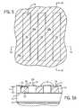
- FIG. 1illustrates a diagrammatic top plan view of a portion of a substrate at a preliminary processing stage according to an embodiment of the present disclosure, showing the substrate with a neutral wetting material thereon.
- FIGS. 1A and 1Bare elevational, cross-sectional views of the substrate depicted in FIG. 1 taken along lines 1 A- 1 A and 1 B- 1 B, respectively.
- FIG. 2illustrates a diagrammatic top plan view of the substrate of FIG. 1 at a subsequent stage showing the formation of trenches in a material layer formed on the neutral wetting material.
- FIGS. 2A and 2Billustrate elevational, cross-sectional views of a portion of the substrate depicted in FIG. 2 taken, respectively, along lines 2 A- 2 A and 2 B- 2 B.
- FIG. 3illustrates a side elevational view of a portion of a substrate at a preliminary processing stage according to another embodiment of the disclosure, showing the substrate with trenches in a material layer formed on the substrate.
- FIG. 4illustrates a side elevational view of the substrate of FIG. 3 at a subsequent stage showing the formation of a neutral wetting material within the trenches.
- FIG. 5is a diagrammatic top plan view of the substrate of FIG. 2 at a subsequent stage showing a block copolymer material within the trenches.
- FIGS. 5A and 5Billustrate elevational, cross-sectional views of a portion of the substrate depicted in FIG. 5 taken along lines 5 A- 5 A and 5 B- 5 B, respectively.
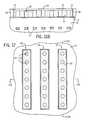
- FIGS. 6-8are diagrammatic top plan views of the substrate of FIG. 5 at subsequent stages showing annealing of a portion of the film according to an embodiment of the invention by a zoned annealing technique.
- FIGS. 6A-8Aillustrate elevational, cross-sectional views of the substrate depicted in FIGS. 6-8 taken along lines 6 A- 6 A, 7 A- 7 A and 8 A- 8 A, respectively, showing an embodiment of a heating device for zone annealing the film.
- FIG. 6Bis an elevational, cross-sectional view of the substrate depicted in FIG. 6 taken along lines 6 B- 6 B.
- FIG. 9is a top plan view of the substrate of FIG. 5 at a subsequent stage according to another embodiment of a method of the invention, illustrating placement of a non-preferential wetting material over the block copolymer material during an anneal.
- FIGS. 9A and 9Bare elevational, cross-sectional views of the substrate depicted in FIG. 9 taken along lines 9 A- 9 A and 9 B- 9 B, respectively.
- FIGS. 10A and 10Bare cross-sectional views of the substrate shown in FIGS. 9A and 9B , respectively, at a subsequent stage showing the annealed, self-assembled block copolymer material, and removal of the non-preferential wetting material after the anneal.
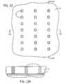
- FIGS. 11-13are top plan views of the substrate of FIG. 8 at subsequent stages, illustrating an embodiment of the use of the self-assembled block copolymer film after removal of one of the polymer blocks, as a mask to etch the substrate and filling of the etched openings.
- FIGS. 11A-13Aillustrate elevational, cross-sectional views of a portion of the substrate depicted in FIGS. 11-13 taken along lines 11 A- 11 A to 13 A- 13 A, respectively.
- FIGS. 11B-13Bare cross-sectional views of the substrate depicted in FIGS. 11-13 taken along lines 11 B- 11 B to 13 B- 13 B, respectively.
- substraterefers to any supporting structure including, but not limited to, the semiconductive substrates, wafer fragments or wafers described above.
- L ois the inherent periodicity or pitch value (bulk period or repeat unit) of structures that self-assemble upon annealing from a self-assembling (SA) block copolymer.
- L Bis the periodicity or pitch value of a blend of a block copolymer with one or more of its constituent homopolymers.
- Lis used herein to indicate the center-to-center cylinder pitch or spacing of cylinders of the block copolymer or blend, and is equivalent to “L o ” for a pure block copolymer and “L B ” for a copolymer blend.
- a polymer materiale.g., film, layer
- a polymer materialis prepared by guided self-assembly of block copolymers, with both polymer domains at the air interface.
- the block copolymer materialspontaneously assembles into periodic structures by microphase separation of the constituent polymer blocks after annealing, faulting ordered domains of perpendicular-oriented cylinders at nanometer-scale dimensions within a trench.
- a method for fabricating a self-assembled block copolymer material that defines a one-dimensional (1D) array of nanometer-scale, perpendicular-oriented cylinders according to an embodiment of the inventionis illustrated with reference to FIGS. 1-8 .
- the described embodimentinvolves a thermal anneal of a cylindrical-phase block copolymer under a solvent atmosphere.
- the annealis conducted in combination with a graphoepitaxy technique that utilizes a lithographically defined trench as a guide with a floor composed of a material that is neutral wetting to both polymer blocks, and sidewalls and ends that are preferential wetting to one polymer block and function as constraints to induce the block copolymer to self-assemble into an ordered 1D array of a single row of cylinders in a polymer matrix oriented perpendicular to the trench floor and registered to the trench sidewalls.
- two or more rows of perpendicular-oriented cylinderscan be formed in each trench.
- a substrate 10is provided, which can be silicon, silicon oxide, silicon nitride, silicon oxynitride, silicon oxycarbide, among other materials.
- conductive lines 12or other active area, e.g., semiconducting regions are situated within the substrate 10 .
- a single trench or multiple trenchescan be formed in the substrate, and can span the entire width of an array of lines (or other active area).
- the substrate 10is provided with an array of conductive lines 12 (or other active areas) at a pitch of L.
- the trench or trenchesare formed over the active areas 12 (e.g., lines) such that when the block copolymer material is annealed, each cylinder will be situated above a single active area 12 (e.g., a conductive line).
- multiple trenches 18are formed with the ends 24 of each adjacent trench 18 aligned or slightly offset from each other at less than 5% of L such that cylinders in adjacent trenches 18 are aligned and situated above the same conductive line 12 .
- a neutral wetting material 14(e.g., random copolymer) has been formed over the substrate 10 .
- a material layer 16(or one or more material layers) can then be formed over the neutral wetting material 14 and etched to form trenches 18 that are oriented perpendicular to the array of conductive lines 12 , as shown in FIGS. 2-2B . Portions of the material layer 16 form a spacer 20 outside and between the trenches.
- the trenches 18are structured with opposing sidewalls 22 , opposing ends 24 , a floor 26 , a width (w t ), a length (l t ) and a depth (D t ).
- the material layer 16 ′can be formed on the substrate 10 ′, etched to faun the trenches 18 ′ as depicted in FIG. 3 , and a neutral wetting material 14 ′ can then be formed on the trench floors 26 ′ as shown in FIG. 4 .
- a random copolymer materialcan be deposited into the trenches 18 ′ and crosslinked to form a neutral wetting material layer. Material on surfaces outside the trenches 18 ′ such as on the spacers 20 ′ (e.g., non-crosslinked random copolymer) can be subsequently removed.
- Single or multiple trenches 18can be formed using a lithographic tool having an exposure system capable of patterning at the scale of L (10-100 nm).
- exposure systemsinclude, for example, extreme ultraviolet (EUV) lithography, proximity X-rays and electron beam (E-beam) lithography, as known and used in the art.
- EUVextreme ultraviolet
- E-beamelectron beam
- Conventional photolithographycan attain (at smallest) about 58 nm features.
- a method called “pitch doubling” or “pitch multiplication”can also be used for extending the capabilities of photolithographic techniques beyond their minimum pitch, as described, for example, in U.S. Pat. No. 5,328,810 (Lowrey et al.), U.S. Pat. No. 7,115,525 (Abatchev, et al.), U.S. Patent Publication 2006/0281266 (U.S. Pat. No. 7,396,781, issued Jul. 8, 2008, to Wells) and U.S. Patent Publication 2007/0023805 (U.S. Pat. No. 7,776,715, issued Aug. 17, 2010, to Wells).
- a pattern of linesis photolithographically formed in a photoresist material overlying a layer of an expendable material, which in turn overlies a substrate, the expendable material layer is etched to form placeholders or mandrels, the photoresist is stripped, spacers are formed on the sides of the mandrels, and the mandrels are then removed, leaving behind the spacers as a mask for patterning the substrate.
- the initial photolithographyformed a pattern defining one feature and one space
- the same widthnow defines two features and two spaces, with the spaces defined by the spacers.
- the smallest feature size possible with a photolithographic techniqueis effectively decreased down to about 30 nm or less.
- Factors in forming a single 1D array or layer of perpendicular-oriented nanocylinders within the trenchesinclude the width (w t ) and depth (D t ) of the trench, the formulation of the block copolymer or blend to achieve the desired pitch (L), and the thickness (t) of the block copolymer material within the trench.
- a block copolymer or blend having a pitch or L value of 35-nm deposited into a 75-nm wide trench 18 having a neutral wetting floorwill, upon annealing, result in a zigzag pattern of 17.5-nm diameter ( ⁇ 0.5*L) perpendicular cylinders that are offset by about one-half the pitch distance (about 0.5*L) for the length (l t ) of the trench 18 , rather than a single line row of perpendicular cylinders aligned with the sidewalls 22 down the center of the trench 18 .
- the trenches 18are constructed with a width (w t ) of about 1.5-2*L (or 1.5-2 ⁇ the pitch value) of the block copolymer such that a cast block copolymer material (or blend) of about L will self-assemble upon annealing into a single row of perpendicular cylinders (diameter ⁇ 0.5*L) with a center-to-center pitch distance (p) of adjacent cylinders at or about L.
- the width (w t ) of the trenches 18can be about 1.5-2*50 nm or about 75-100 nm.
- the length (l t ) of the trenches 18is at or about n*L or an integer multiple of L, typically within a range of about n*10 to about n*100 nm (with n being the number of features or structures, e.g., cylinders).
- the depth (D t ) of the trenches 18is greater than or equal to L (D t >L)
- the width of the spacers 20 between adjacent trenchescan vary and is generally about L to about n*L.
- the trench dimensionis about 20-100 nm wide (w t ) and about 100-25,000 nm in length (l t ), with a depth (D t ) of about 10-100 nm.
- a self-assembling, cylindrical-phase block copolymer material 28 having an inherent pitch at or about L o (or a ternary blend of block copolymer and homopolymers blended to have a pitch at or about L B )is deposited into the trenches 18 , typically as a film (as in FIGS. 5-5B ).
- the block copolymer(or blend) is constructed such that all of the polymer blocks will have equal preference for a neutral wetting material on the trench floor.
- the block copolymer materialcan be constructed to provide desired properties such as defect tolerance and ease of development and/or removal of one of the blocks.
- the block copolymer or blendis constructed such that the minor domain can be selectively removed.
- diblock copolymersinclude, for example, poly(styrene)-b-poly(vinylpyridine) (PS-b-PVP), poly(styrene)-b-poly(methyl methacrylate) (PS-b-PMMA) or other PS-b-poly(acrylate) or PS-b-poly(methacrylate), poly(styrene)-b-poly(lactide) (PS-b-PLA), poly(styrene)-b-poly(tert-butyl acrylate) (PS-b-PtBA), and poly(styrene)-b-poly(ethylene-co-butylene (PS-b-(PS-co-PB)), poly(styrene)-b-poly(ethylene oxide) (PS-b-PEO), poly(isoprene)-b-poly(ethyleneoxide) (PI-b-PEO), poly(isoprene)-b-poly(methyl meth
- PS-b-PMMA block copolymer doped with PEO-coated gold nanoparticles of a size less than the diameter of the self-assembled cylindersPark et al., Macromolecules, 2007, 40(11), 8119-8124
- PS-b-P2VPpoly(styrene)-b-poly(2-vinylpyridine)
- PS-b-P2VPpoly(styrene)-b-poly(2-vinylpyridine) block copolymer having a cleavable junction such as a dithiol group, among others, with PS-b-PVP used in the illustrated embodiment.
- Other types of block copolymersi.e., triblock or multiblock copolymers can be used.
- triblock copolymersexamples include ABC copolymers such as poly(styrene-b-methyl methacrylate-b-ethylene oxide) (PS-b-PMMA-b-PEO), and ABA copolymers, such as PS-PMMA-PS, PMMA-PS-PMMA, and PS-b-PI-b-PS, among others.
- ABC copolymerssuch as poly(styrene-b-methyl methacrylate-b-ethylene oxide) (PS-b-PMMA-b-PEO)
- ABA copolymerssuch as PS-PMMA-PS, PMMA-PS-PMMA, and PS-b-PI-b-PS, among others.
- the film morphologyincluding the domain sizes and periods (L o ) of the microphase-separated domains, can be controlled by chain length of a block copolymer (molecular weight, MW) and volume fraction of the AB blocks of a diblock copolymer to produce cylindrical morphologies (among others).
- a block copolymermolecular weight, MW
- volume fraction of the AB blocks of a diblock copolymerto produce cylindrical morphologies (among others).
- the diblock copolymerwill microphase separate and self-assemble into periodic cylindrical domains of polymer B within a matrix of polymer A.
- An example of a cylinder-forming PS-b-PVP copolymer material (L o ⁇ 28 nm) to form about 14 nm diameter cylindrical PVP domains in a matrix of PSis composed of about 70 wt % PS and 30 wt % PVP with a total molecular weight (M n ) of 44.5 kg/mol.
- the L value of the block copolymercan be modified, for example, by adjusting the molecular weight of the block copolymer.
- the block copolymer materialcan also be formulated as a binary or ternary blend comprising a block copolymer and one or more homopolymers (HPs) of the same type of polymers as the polymer blocks in the block copolymer, to produce a blend that will swell the size of the polymer domains and increase the L value.
- the concentration of homopolymers in the blendcan range from 0 to about 60 wt %.
- a ternary diblock copolymer blendis a PS-b-P2VP/PS/P2VP blend, for example, 60 wt % of 32.5 K/12 K PS-b-P2VP, 20 wt % of 10 K PS, and 20 wt % of 10 K P2VP.
- Another example of a ternary diblock copolymer blendis a PS-b-PMMA/PS/PMMA blend, for example, 60 wt % of 46K/21K PS-b-PMMA, 20 wt % of 20K polystyrene and 20 wt % of 20K poly(methyl methacrylate).
- Yet another exampleis a blend of 60:20:20 (wt %) of PS-b-PEO/PS/PEO, or a blend of about 85-90 wt % PS-b-PEO and up to 10-15 wt % PEO; it is believed that the added PEO homopolymer may function, at least in part, to lower the surface energy of the PEO domains to that of PS.
- the trench floors 26are structured to be neutral wetting (equal affinity for both blocks of the copolymer) to induce formation of cylindrical polymer domains that are oriented perpendicular to the trench floors 26
- the trench sidewalls 22 and ends 24are structured to be preferential wetting by one block of the block copolymer to induce registration of the cylinders to the sidewalls 22 as the polymer blocks self-assemble.
- the preferred or minority block of the cylindrical-phase block copolymerwill self-assemble to form a single row of cylindrical domains in the center of a polymer matrix for the length of the trench and segregate to the sidewalls and edges of the trench to form a thin interface brush or wetting layer (e.g., as in FIGS. 6-6B ).
- Entropic forcesdrive the wetting of a neutral wetting surface by both blocks, and enthalpic forces drive the wetting of a preferential-wetting surface by the preferred block (e.g., the minority block).
- the material layer 16can be composed of silicon (with native oxide), oxide (e.g., silicon oxide, SiO x ), silicon nitride, silicon oxycarbide, indium tin oxide (ITO), silicon oxynitride, and resist materials such as methacrylate-based resists and polydimethylglutarimide resists, among other materials, which exhibit preferential wetting toward the PVP (or PMMA, etc.) block.
- oxidee.g., silicon oxide, SiO x
- silicon nitridesilicon oxycarbide
- ITOindium tin oxide
- resist materialssuch as methacrylate-based resists and polydimethylglutarimide resists, among other materials, which exhibit preferential wetting toward the PVP (or PMMA, etc.) block.
- the block copolymer materialwill self-assemble to form a thin interface layer and cylinders of PVP in a PS matrix.
- a preferential wetting materialsuch as a polymethyl methacrylate (PMMA) polymer modified with an —OH containing moiety (e.g., hydroxyethylmethacrylate) can be applied onto the surfaces of the trenches, for example, by spin-coating and then heating (e.g., to about 170° C.) to allow the terminal OH groups to end-graft to oxide sidewalls 22 and ends 24 of the trenches 18 .
- Non-grafted materialcan be removed by rinsing with an appropriate solvent (e.g., toluene). See, for example, Mansky et al., Science, 1997, 275, 1458-1460, and In et al., Langmuir, 2006, 22, 7855-7860.
- a neutral wetting trench floor 26allows both blocks of the copolymer material to wet the floor 26 of the trench 18 .
- a neutral wetting material 14can be provided by applying a neutral wetting polymer (e.g., a neutral wetting random copolymer) onto the substrate 10 , forming the material layer 16 and then etching the trenches 18 to expose the underlying neutral wetting material, as illustrated in FIGS. 2-2B .
- a neutral wetting polymere.g., a neutral wetting random copolymer
- a neutral wetting random copolymer materialcan be applied after forming the trenches 18 ′, for example, as a blanket coat by casting or spin-coating into the trenches 18 ′, as depicted in FIG. 4 .
- the random copolymer materialcan then be thermally processed to flow the material into the bottom of the trenches 18 ′ by capillary action, which results in a layer (mat) 14 ′ composed of the crosslinked, neutral wetting random copolymer.
- the random copolymer material within the trenches 18 ′can be photo-exposed (e.g., through a mask or reticle) to crosslink the random copolymer within the trenches 18 ′ to form the neutral wetting material 14 ′.
- Non-crosslinked random copolymer material outside the trenchese.g., on the spacers 20 ′
- Neutral wetting surfacescan be specifically prepared by the application of random copolymers composed of monomers identical to those in the block copolymer and tailored such that the mole fraction of each monomer is appropriate to form a neutral wetting surface.
- a neutral wetting material 14can be formed from a thin film of a photo-crosslinkable random PS-r-PVP that exhibits non-preferential or neutral wetting toward PS and PVP, which can be cast onto the substrate 10 (e.g., by spin-coating).
- the random copolymer materialcan be fixed in place by chemical grafting (on an oxide substrate) or by thermally or photolytically crosslinking (any surface) to form a mat that is neutral wetting to PS and PVP and insoluble when the block copolymer material is cast onto it, due to the crosslinking.
- a photo-crosslinkable PS-r-PMMA random copolymere.g., containing an about 0.6 mole fraction of styrene
- another neutral wetting surface for PS-b-PMMAcan be provided by hydrogen-terminated silicon.
- the floors 26 of the trenches 18can be etched, for example, with a hydrogen plasma, to remove the oxide material and form hydrogen-terminated silicon, which is neutral wetting with equal affinity for both blocks of a block copolymer material.
- H-terminated siliconcan be prepared by a conventional process, for example, by a fluoride ion etch of a silicon substrate (with native oxide present, about 12-15 ⁇ ) by exposure to an aqueous solution of hydrogen fluoride (HF) and buffered HF or ammonium fluoride (NH 4 F), by HF vapor treatment, or by a hydrogen plasma treatment (e.g., atomic hydrogen).
- a fluoride ion etch of a silicon substratewith native oxide present, about 12-15 ⁇
- HFhydrogen fluoride
- NH 4 Fbuffered HF or ammonium fluoride
- HF vapor treatmente.g., atomic hydrogen
- An H-terminated silicon substratecan be further processed by grafting a random copolymer such as PS-r-PVP, PS-r-PMMA, etc. selectively onto the substrate resulting in a neutral wetting surface for the corresponding block copolymer (e.g., PS-b-PVP, PS-b-PMMA, etc.).
- a neutral wetting layer of a PS-r-PMMA random copolymercan be provided by an in situ free radical polymerization of styrene and methyl methacrylate using a di-olefinic linker such as divinyl benzene, which links the polymer to the surface to produce about a 10-15 nm thick film.
- a neutral wetting random copolymer material 14 ′can be applied after formation of the material layer 16 ′ and trenches 18 ′, which reacts selectively with the trench floor 26 ′ (composed of the substrate 10 ′ material) and not the trench sidewalls 22 ′ or ends 24 ′ (composed of the material layer 16 ′).
- a random copolymer (or appropriate blend of homopolymers with block copolymer surfactant) containing epoxide groupswill react selectively to terminal amine functional groups (e.g. —NH— and —NH 2 ) on silicon nitride and silicon oxynitride surfaces relative to silicon oxide or silicon.
- the trench floor 26 ′is silicon or polysilicon and the sidewalls 22 ′ are a material such as an oxide (e.g., SiO x )
- the trench floor 26 ′can be treated to form H-terminated silicon and a random copolymer material 14 ′ (e.g., PS-r-PVP, PS-r-PMMA, etc.) can be formed in situ only at the floor surface.
- a random copolymer material 14 ′e.g., PS-r-PVP, PS-r-PMMA, etc.
- a neutral wetting surface(e.g., for PS-b-PMMA and PS-b-PEO) can be provided by grafting a self-assembled monolayer (SAM) of a trichlorosilane-base SAM such as 3-(para-methoxyphenyl)propyltrichorosilane grafted to oxide (e.g., SiO 2 ) as described, for example, by D. H. Park, Nanotechnology 18 (2007), p. 355304.
- SAMself-assembled monolayer
- oxidee.g., SiO 2
- a neutral wetting random copolymer of polystyrene (PS), polymethacrylate (PMMA) with hydroxyl group(s)e.g., 2-hydroxyethyl methacrylate (P(S-r-MMA-r-HEMA)
- PMMApolymethacrylate
- P(S-r-MMA-r-HEMA)2-hydroxyethyl methacrylate
- a substrate 10e.g., an oxide
- a neutral wetting layer 14about 5-10 nm thick by heating at about 160° C. for about 48 hours. See, for example, In et al., Langmuir, 2006, 22, 7855-7860.
- a blend of hydroxyl-terminated homopolymers and a corresponding low molecular weight block copolymercan be grafted (covalently bonded) to the substrate to form a neutral wetting interface layer (e.g., about 4-5 nm) for PS-b-PMMA and PS-b-P2VP, among other block copolymers.
- the block copolymercan function to emulsify the homopolymer blend before grafting.
- a solvent rinsee.g., toluene
- a surface that is neutral wetting to PS-b-PMMAcan also be prepared by spin-coating a blanket layer of a photo- or thermally cross-linkable random copolymer such as a benzocyclobutene- or azidomethylstyrene-functionalized random copolymer of styrene and methyl methacrylate (e.g., poly(styrene-r-benzocyclobutene-r-methyl methacrylate (PS-r-PMMA-r-BCB)).
- a photo- or thermally cross-linkable random copolymersuch as a benzocyclobutene- or azidomethylstyrene-functionalized random copolymer of styrene and methyl methacrylate (e.g., poly(styrene-r-benzocyclobutene-r-methyl methacrylate (PS-r-PMMA-r-BCB)).
- such a random copolymercan comprise about 42 wt % PMMA, about (58 ⁇ x) wt % PS and x wt % (e.g., about 2-3 wt %) of either polybenzocyclobutene or poly(para-azidomethylstyrene)).
- An azidomethylstyrene-functionalized random copolymercan be UV photo-crosslinked (e.g., 1-5 MW/cm 2 exposure for about 15 seconds to about 30 minutes) or thermally crosslinked (e.g., at about 170° C. for about 4 hours) to form a crosslinked polymer mat as a neutral wetting layer 14 .
- a benzocyclobutene-functionalized random copolymercan be thermally crosslinked (e.g., at about 200° C. for about 4 hours or at about 250° C. for about 10 minutes).
- a self-assembling, cylindrical-phase block copolymer material 28 having an inherent pitch at or about L o(or a ternary blend of block copolymer and homopolymers blended to have a pitch at or about L B ) can be cast or deposited into the trenches 18 to a thickness (t 1 ) at or about the L value of the block copolymer material 28 (e.g., about ⁇ 20% of L) such that after annealing (e.g., FIG.
- the thickness (t 2 )will be at or about the L value and the block copolymer material 28 will self-assemble to form a single layer of cylinders having a diameter of about 0.5*L (e.g., 5-50 nm, or about 20 nm, for example) within a polymer matrix in a single row within each trench 18 .
- the thickness of the block copolymer material 28can be measured, for example, by ellipsometry techniques.
- the block copolymer material 28can be deposited by spin-casting (spin-coating) from a dilute solution (e.g., about 0.25-2 wt % solution) of the copolymer in an organic solvent such as dichloroethane (CH 2 Cl 2 ) or toluene, for example. Capillary forces pull excess block copolymer material 28 (e.g., greater than a monolayer) into the trenches 18 . As shown, a thin layer or film 28 a of the block copolymer material 28 can be deposited onto the material layer 16 outside the trenches 18 , e.g., on the spacers 20 . Upon annealing, the thin film 28 a will flow into the trenches 18 leaving a structureless brush layer on the material layer 16 from a top-down perspective.
- a dilute solutione.g., about 0.25-2 wt % solution
- organic solventsuch as dichloroethane (CH 2 Cl 2 ) or tol
- the block copolymer (BCP) material 28is then heated above its glass transition temperature under a vapor phase containing a partly-saturated concentration of an organic solvent to cause the polymer blocks to phase separate and self-assemble according to the preferential and neutral wetting of the trench surfaces to form a self-assembled polymer material 30 , as illustrated in FIGS. 6-6B .
- the appropriate partial pressure of solvent vapor to achieve a neutral wetting vapor interface at a particular temperaturedepends, at least in part, on the block copolymer that is used and can be determined empirically.
- the block copolymeris heated at a thermal anneal temperature that is above its glass transition temperature (T g ) but below the decomposition or degradation temperature (T d ) of the block copolymer material.
- a PS-b-PVP block copolymer materialcan be annealed at a temperature of about 150° C.-275° C. in a solvent vapor atmosphere for about 1-24 hours to achieve a self-assembled morphology.
- a PS-b-PMMA block copolymer materialcan be annealed at a temperature of about 150° C.-275° C. in a solvent vapor atmosphere for about 1-24 hours to achieve a self-assembled morphology.
- an air interfaceis preferentially wetting to one of the polymer domains and the BCP material does not orient into perpendicular structures.
- the BCP material 28is exposed to solvent vapors of a “good” solvent for both blocks, that is, a neutral organic solvent that solvates both the constituent blocks well.
- solvent annealingconsists of two phases.
- a first phasethe BCP material is exposed to a solvent vapor that acts to plasticize the film and increase chain mobility causing the domains to intermingle and the loss of order inherent from casting the polymer material.
- the organic solvent that is utilizedis based at least in part on its solubility in the block copolymer material such that sufficient solvent molecules enter the block copolymer material to promote the order-disorder transition of the polymer domains and enable the required molecular rearrangement.
- solventsexamples include aromatic solvents such as benzene, toluene, xylene, dimethoxyethane, ethyl acetate, cyclohexanone, etc., and chlorinated solvents such as chloroform, methylene chloride, a chloroform/octane mixture, etc., among others.
- aromatic solventssuch as benzene, toluene, xylene, dimethoxyethane, ethyl acetate, cyclohexanone, etc.
- chlorinated solventssuch as chloroform, methylene chloride, a chloroform/octane mixture, etc., among others.
- the evaporation of the solventis highly directional and forms a solvent gradient from the “top” (surface) of the BCP material to the “bottom” of the BCP material at the trench floor that induces orientation and self-assembly of structures starting at the air-surface interface, which is neutral wetting due to the partial pressure of solvent at the interface, and driven downward to the floor of the trench, with formation of perpendicular-oriented cylindrical domains 34 guided by the trench sidewalls and extending completely from the air interface to the substrate surface (trench floor).
- the substrate 10 and BCP material 28are heated above the boiling point of the solvent such that swelling of the BCP material 28 by the solvent is disallowed.
- the use of a partly-saturated solvent vapor phase above the block copolymer material 28provides a neutral wetting interface, similar to the second phase of solvent annealing.
- the concentration of solvent in the air immediate at the vapor interface with the BCP material 28is maintained at or under saturation to maintain a neutral wetting interface such that both (or all) polymer blocks will equally wet the vapor interface.
- both the air and trench floor 26are neutral wetting, the domains will orient perpendicular throughout the film layer, with the preferential wetting sidewalls inducing lateral order.
- the resulting morphology of the annealed copolymer material 30can be examined, for example, using atomic force microscopy (AFM), transmission electron microscopy (TEM), scanning electron microscopy (SEM), among others.
- AFMatomic force microscopy
- TEMtransmission electron microscopy
- SEMscanning electron microscopy
- the annealis performed by globally heating the block copolymer within the trenches in a solvent atmosphere.
- a zone annealingis conducted to anneal portions or sections of the block copolymer material 28 in trenches on the substrate 10 by a localized application of thermal energy (e.g., heat). Zone annealing can provide rapid self-assembly of the block copolymer material (e.g., on the order of minutes).
- thermal energye.g., heat
- the substrate 10in a vapor atmosphere
- a thermal or heat source 32(or combined heating and cooling source) can be moved relative to each other (e.g., arrow ⁇ ) such that heat is applied above (or underneath) the substrate 10 .
- Only a portion of the BCP material 28is initially heated above the glass transition temperature and the heated zone is then “pulled” across the substrate 10 (or vice versa).
- the thermal or heat source 32can be moved across the substrate 10 at a translational set speed (e.g., about 0.05-10 ⁇ m/second using a mechanism such as a motorized translation stage (not shown). Pulling the heated zone across the substrate 10 (or vice versa) can result in faster processing and better ordered structures relative to a global thermal anneal.
- a hot-to-cold temperature gradientcan be provided over (or under) the substrate such that a certain portion of the substrate is heated and then cooled, which can be at a controlled rate.
- the substratecan be exposed to a cold-to-hot temperature gradient to anneal the BCP material, followed by cooling.
- the BCP materialcan be heated above and then cooled below the order-disorder temperature (but above the glass transition temperature), for example, to remove (melt out) defects and allow the material to recrystallize provided that the order-disorder temperature (T o-d ) is less than the decomposition temperature (T d ) of the block copolymer material.
- the order-disorder temperatureis defined by the temperature dependence of the block copolymer, Chi value, the total number of monomers per chain, and the monomer composition.
- the block copolymer material 28 within trench 18 acan be heated and annealed to form a self-assembled material 30 while the unannealed block copolymer material 28 within trenches 18 b , 18 c remains disordered. Only those portions of the block copolymer material 28 that are heated above the glass transition temperature (T g ) will self-assemble. A next portion of the substrate 10 can then be selectively heated, as shown in FIGS.
- a subsequent heating of the remaining areas of the substrate 10can then be conducted, e.g., as depicted in FIGS. 8 and 8A .
- the cylindrical-phase block copolymer material 28Upon annealing, the cylindrical-phase block copolymer material 28 will self-assemble into a polymer material 30 (e.g., film) in response to the character of the block copolymer composition (e.g., PS-b-PVP having an inherent pitch at or about L) and the boundary conditions, including the constraints provided by the width (w t ) of the trench 18 and the wetting properties of the trench surfaces including a trench floor 26 that exhibits neutral or non-preferential wetting toward both polymer blocks (e.g., a random graft copolymer), sidewalls 22 that are preferential wetting by the minority (preferred) block of the block copolymer (e.g., the PVP block), and the presence of a neutral or non-preferential solvent (or in some embodiments, a film or material that is neutral or non-preferential wetting) in contact with the surface of the block copolymer material 28 in the trenches 18 .
- the annealresults in a row (or rows) of perpendicularly-oriented cylinders 34 of the minority polymer (preferred) block (e.g., PVP) within a matrix 36 of the majority polymer block (e.g., PS), with the cylinders 34 registered and parallel to the sidewalls 22 of the trenches 18 .
- the diameter of the cylinders 34will generally be at or about 0.5*L (e.g., about one-half of the center-to-center distance between cylinders).
- the minority (preferred) blocke.g., PVP
- PVPminority (preferred) block
- the minority (preferred) blockwill segregate to and wet the preferential wetting sidewalls 22 and ends 24 of the trenches 18 to fog n a thin interface or wetting brush layer 34 a having a thickness generally about one-fourth of the center-to-center distance between adjacent cylinders 34 .
- a layer of the PVP blockwill wet oxide interfaces with attached PS domains directed outward from the oxide material.
- the self-assembled block copolymer material 30is defined by a single layer of an array of cylindrical domains (cylinders) 34 , each with a diameter at or about 0.5*L (e.g., about one-half of the center-to-center distance between cylinders), with the number (n) of cylinders in the row according to the length (l t ) of the trench, and the center-to-center distance (pitch distance, p) between each cylinder at or about L.
- Lcenter-to-center distance
- the copolymer materialcan be treated to crosslink the polymer segments (e.g., the PS segments) to fix and enhance the strength of the self-assembled polymer blocks.
- the polymerscan be structured to inherently crosslink (e.g., upon exposure to ultraviolet (UV) radiation, including deep ultraviolet (DUV) radiation), or one of the polymer blocks of the copolymer material can be formulated to contain a crosslinking agent.
- the film 28 a outside the trenches 18 a , 18 b , 18 c(e.g., on spacers 20 ) will not be thick enough to result in self-assembly.
- the unstructured thin film 28 acan be removed, as illustrated in FIGS. 8 and 8A , for example, by an etch technique or a planarization process to provide an about uniformly flat surface.
- the trench regionscan be selectively exposed through a reticle (not shown) to crosslink only the annealed and self-assembled polymer material 30 within the trenches 18 a , 18 b , 18 c , and a wash can then be applied with an appropriate solvent (e.g., toluene) to remove the non-crosslinked portions of the block copolymer material 28 (e.g., on the spacers 20 ), leaving the registered self-assembled polymer material 30 within the trenches 18 a , 18 b , 18 c and exposing the surface of the material layer 16 above/outside the trenches 18 a , 18 b , and 18 c .
- an appropriate solvente.g., toluene
- the annealed polymer material 30can be crosslinked globally, a photoresist material can be applied to pattern and expose the areas of the polymer material 28 a outside the trench regions, and the exposed portions of the polymer material 28 a can be removed, for example, by an oxygen (O 2 ) plasma treatment.
- O 2oxygen
- a thermal annealis conducted while applying a non-preferentially wetting material 37 ′ to the surface of the block copolymer (BCP) material 28 ′ in the trenches.
- the non-preferentially wetting material 37 ′is composed of a solid material, which can be physically placed onto the BCP material 28 ′, for example, a soft, flexible or rubbery solid material such as a cross-linked, poly(dimethylsiloxane) (PDMS) elastomer (e.g., SYLGARD® 184 by Dow-Corning) or other elastomeric polymer material (e.g., silicones, polyurethanes, etc.), which provides an external surface that is neutral wetting.
- PDMSpoly(dimethylsiloxane)
- SYLGARD® 184by Dow-Corning
- other elastomeric polymer materiale.g., silicones, polyurethanes, etc.
- the solid materialcan be derivatized (e.g., by grafting a random copolymer) such that it presents a neutral wetting surface.
- a thermal annealing processis conducted (arrows ⁇ , FIGS. 9A and 9B ) to cause the polymer blocks to phase separate in response to the preferential and neutral wetting of the trench surfaces and the non-preferential (neutral) wetting of the overlying material 37 ′, and form a self-assembled polymer material 30 ′ as illustrated in FIGS. 10A and 10B .
- the non-preferentially wetting material 37 ′can be removed from contact with the annealed polymer material 30 ′ (arrow ⁇ ) as depicted in FIG. 10A .
- a PDMS or other elastomeric material layer 37 ′can be removed, for example, by lifting or peeling the material from the surface of the annealed copolymer material 30 ′.
- a solventsuch as water, alcohols, and the like, which is compatible with and does not dissolve the block copolymer material 30 ′, can be applied (e.g., by soaking) to permeate and swell the elastomeric material (e.g., PDMS) to enhance physical removal.
- a dilute fluoride solutione.g., NH 4 F, HF, NaF, etc.
- the pattern of perpendicular-oriented cylinders 34 ′ that is formed on the substrate 10 ′can then be further processed as desired, for example, to form an etch mask for patterning nanosized features into the underlying substrate 10 ′ through selective removal of one block of the self-assembled block copolymer.
- MWchain length of a block copolymer
- resolutioncan exceed other techniques such as conventional photolithography. Processing costs using the technique is significantly less than extreme ultraviolet (EUV) photolithography, which has comparable resolution.
- EUVextreme ultraviolet
- an etch mask 38can be formed by selectively removing the cylindrical polymer domains 34 of the self-assembled polymer material 30 to produce openings 40 in the polymer matrix 36 (e.g., PS) to expose the underlying substrate 10 at the trench floors 26 .
- the cylindrical domains 34can be removed by a selective wet etch (e.g., PMMA and PLA by UV exposure/acetic acid development, PLA by aqueous methanol mixture containing sodium hydroxide, PEO by aqueous hydroiodic acid or water, etc.) or by a selective reactive ion etch (RIE) process.
- a selective wet etche.g., PMMA and PLA by UV exposure/acetic acid development, PLA by aqueous methanol mixture containing sodium hydroxide, PEO by aqueous hydroiodic acid or water, etc.
- RIEselective reactive ion etch
- the filmcan be exposed to a solvent selective to the minor domain, for example, an alcohol for PVP, water for PEO or PLA, and acetic acid for PMMA, that contains a cleaving agent to remove (e.g., wash out) the minor domain.
- a solvent selective to the minor domainfor example, an alcohol for PVP, water for PEO or PLA, and acetic acid for PMMA, that contains a cleaving agent to remove (e.g., wash out) the minor domain.
- the remaining porous polymer (e.g., PS) matrix 36can then be used as a lithographic template or mask to etch (arrows ⁇ ) a series of cylindrical-shaped openings or contact holes 42 in the nanometer size range (e.g., about 10-100 nm) to the conductive lines 12 or other active area (e.g., semiconducting region, etc.) in the underlying substrate 10 (or an underlayer).
- the openings 42can be formed, for example, using a selective reactive ion etching (RIE) process.
- the residual polymer matrix 36can be removed (e.g., PS by an oxidation process such as a plasma O 2 etch) and the openings 42 of substrate 10 can be filled with a material 44 such as a metal or metal alloy such as Cu, Al, W, Si, and Ti 3 N 4 , among others, to form arrays of cylindrical contacts to the conductive lines 12 .
- the cylindrical openings 42 in the substrate 10can also be filled with a metal-insulator-metal stack to form capacitors with an insulating material such as SiO 2 , Al 2 O 3 , HfO 2 , ZrO 2 , SrTiO 3 , and the like.
- Embodiments of the inventionutilize a thermal anneal process in combination with solvent annealing, which can provide faster processing than with a solvent anneal alone and expands the types of block copolymers (BCPs) that can be processed to substantially all BCPs.
- BCPsblock copolymers
- a wide range of block copolymerscan be processed to form perpendicular-oriented nanostructures (e.g., cylinders) and at a rapid rate.
- methods of the disclosureprovide a means of generating self-assembled diblock copolymer films composed of perpendicular-oriented cylinders in a polymer matrix.
- the methodsprovide ordered and registered elements on a nanometer scale that can be prepared more inexpensively than by electron beam lithography, EUV photolithography or conventional photolithography.
- the feature sizes produced and accessible by this inventioncannot be easily prepared by conventional photolithography.
- the described methods and systemscan be readily employed and incorporated into existing semiconductor manufacturing process flows and provide a low cost, high-throughput technique for fabricating small structures.
Landscapes
- Engineering & Computer Science (AREA)
- Chemical & Material Sciences (AREA)
- Manufacturing & Machinery (AREA)
- Physics & Mathematics (AREA)
- General Physics & Mathematics (AREA)
- Microelectronics & Electronic Packaging (AREA)
- Condensed Matter Physics & Semiconductors (AREA)
- Computer Hardware Design (AREA)
- Power Engineering (AREA)
- Nanotechnology (AREA)
- Inorganic Chemistry (AREA)
- Chemical Kinetics & Catalysis (AREA)
- Polymers & Plastics (AREA)
- Medicinal Chemistry (AREA)
- Organic Chemistry (AREA)
- Health & Medical Sciences (AREA)
- Analytical Chemistry (AREA)
- Composite Materials (AREA)
- Crystallography & Structural Chemistry (AREA)
- Materials Engineering (AREA)
- General Chemical & Material Sciences (AREA)
- Optics & Photonics (AREA)
- Exposure Of Semiconductors, Excluding Electron Or Ion Beam Exposure (AREA)
- Treatments Of Macromolecular Shaped Articles (AREA)
- Manufacture Of Macromolecular Shaped Articles (AREA)
- Formation Of Insulating Films (AREA)
- Application Of Or Painting With Fluid Materials (AREA)
Abstract
Description
Claims (25)
Priority Applications (4)
| Application Number | Priority Date | Filing Date | Title |
|---|---|---|---|
| US13/469,697US8633112B2 (en) | 2008-03-21 | 2012-05-11 | Thermal anneal of block copolymer films with top interface constrained to wet both blocks with equal preference |
| US14/104,304US9315609B2 (en) | 2008-03-21 | 2013-12-12 | Thermal anneal of block copolymer films with top interface constrained to wet both blocks with equal preference |
| US15/090,144US10153200B2 (en) | 2008-03-21 | 2016-04-04 | Methods of forming a nanostructured polymer material including block copolymer materials |
| US16/215,242US11282741B2 (en) | 2008-03-21 | 2018-12-10 | Methods of forming a semiconductor device using block copolymer materials |
Applications Claiming Priority (2)
| Application Number | Priority Date | Filing Date | Title |
|---|---|---|---|
| US12/052,956US8426313B2 (en) | 2008-03-21 | 2008-03-21 | Thermal anneal of block copolymer films with top interface constrained to wet both blocks with equal preference |
| US13/469,697US8633112B2 (en) | 2008-03-21 | 2012-05-11 | Thermal anneal of block copolymer films with top interface constrained to wet both blocks with equal preference |
Related Parent Applications (1)
| Application Number | Title | Priority Date | Filing Date |
|---|---|---|---|
| US12/052,956ContinuationUS8426313B2 (en) | 2008-03-21 | 2008-03-21 | Thermal anneal of block copolymer films with top interface constrained to wet both blocks with equal preference |
Related Child Applications (1)
| Application Number | Title | Priority Date | Filing Date |
|---|---|---|---|
| US14/104,304DivisionUS9315609B2 (en) | 2008-03-21 | 2013-12-12 | Thermal anneal of block copolymer films with top interface constrained to wet both blocks with equal preference |
Publications (2)
| Publication Number | Publication Date |
|---|---|
| US20120223053A1 US20120223053A1 (en) | 2012-09-06 |
| US8633112B2true US8633112B2 (en) | 2014-01-21 |
Family
ID=40612928
Family Applications (5)
| Application Number | Title | Priority Date | Filing Date |
|---|---|---|---|
| US12/052,956Active2029-12-24US8426313B2 (en) | 2008-03-21 | 2008-03-21 | Thermal anneal of block copolymer films with top interface constrained to wet both blocks with equal preference |
| US13/469,697ActiveUS8633112B2 (en) | 2008-03-21 | 2012-05-11 | Thermal anneal of block copolymer films with top interface constrained to wet both blocks with equal preference |
| US14/104,304ActiveUS9315609B2 (en) | 2008-03-21 | 2013-12-12 | Thermal anneal of block copolymer films with top interface constrained to wet both blocks with equal preference |
| US15/090,144Active2028-10-27US10153200B2 (en) | 2008-03-21 | 2016-04-04 | Methods of forming a nanostructured polymer material including block copolymer materials |
| US16/215,242Active2029-06-16US11282741B2 (en) | 2008-03-21 | 2018-12-10 | Methods of forming a semiconductor device using block copolymer materials |
Family Applications Before (1)
| Application Number | Title | Priority Date | Filing Date |
|---|---|---|---|
| US12/052,956Active2029-12-24US8426313B2 (en) | 2008-03-21 | 2008-03-21 | Thermal anneal of block copolymer films with top interface constrained to wet both blocks with equal preference |
Family Applications After (3)
| Application Number | Title | Priority Date | Filing Date |
|---|---|---|---|
| US14/104,304ActiveUS9315609B2 (en) | 2008-03-21 | 2013-12-12 | Thermal anneal of block copolymer films with top interface constrained to wet both blocks with equal preference |
| US15/090,144Active2028-10-27US10153200B2 (en) | 2008-03-21 | 2016-04-04 | Methods of forming a nanostructured polymer material including block copolymer materials |
| US16/215,242Active2029-06-16US11282741B2 (en) | 2008-03-21 | 2018-12-10 | Methods of forming a semiconductor device using block copolymer materials |
Country Status (7)
| Country | Link |
|---|---|
| US (5) | US8426313B2 (en) |
| EP (1) | EP2281299B1 (en) |
| JP (1) | JP5136869B2 (en) |
| KR (1) | KR101121303B1 (en) |
| CN (1) | CN101978469B (en) |
| TW (1) | TWI391992B (en) |
| WO (1) | WO2009117243A1 (en) |
Cited By (7)
| Publication number | Priority date | Publication date | Assignee | Title |
|---|---|---|---|---|
| US20140256145A1 (en)* | 2013-03-11 | 2014-09-11 | International Business Machines Corporation | Dsa grapho-epitaxy process with etch stop material |
| US9276059B2 (en) | 2007-04-18 | 2016-03-01 | Micron Technology, Inc. | Semiconductor device structures including metal oxide structures |
| US9431605B2 (en) | 2011-11-02 | 2016-08-30 | Micron Technology, Inc. | Methods of forming semiconductor device structures |
| US9876075B2 (en) | 2015-10-16 | 2018-01-23 | International Business Machines Corporation | Method of forming dielectric with air gaps for use in semiconductor devices |
| US10005308B2 (en) | 2008-02-05 | 2018-06-26 | Micron Technology, Inc. | Stamps and methods of forming a pattern on a substrate |
| US10049874B2 (en) | 2013-09-27 | 2018-08-14 | Micron Technology, Inc. | Self-assembled nanostructures including metal oxides and semiconductor structures comprised thereof |
| US10153200B2 (en) | 2008-03-21 | 2018-12-11 | Micron Technology, Inc. | Methods of forming a nanostructured polymer material including block copolymer materials |
Families Citing this family (107)
| Publication number | Priority date | Publication date | Assignee | Title |
|---|---|---|---|---|
| US8394483B2 (en) | 2007-01-24 | 2013-03-12 | Micron Technology, Inc. | Two-dimensional arrays of holes with sub-lithographic diameters formed by block copolymer self-assembly |
| US8083953B2 (en)* | 2007-03-06 | 2011-12-27 | Micron Technology, Inc. | Registered structure formation via the application of directed thermal energy to diblock copolymer films |
| US8557128B2 (en) | 2007-03-22 | 2013-10-15 | Micron Technology, Inc. | Sub-10 nm line features via rapid graphoepitaxial self-assembly of amphiphilic monolayers |
| US7959975B2 (en) | 2007-04-18 | 2011-06-14 | Micron Technology, Inc. | Methods of patterning a substrate |
| US8294139B2 (en) | 2007-06-21 | 2012-10-23 | Micron Technology, Inc. | Multilayer antireflection coatings, structures and devices including the same and methods of making the same |
| US8372295B2 (en) | 2007-04-20 | 2013-02-12 | Micron Technology, Inc. | Extensions of self-assembled structures to increased dimensions via a “bootstrap” self-templating method |
| US8404124B2 (en) | 2007-06-12 | 2013-03-26 | Micron Technology, Inc. | Alternating self-assembling morphologies of diblock copolymers controlled by variations in surfaces |
| US8080615B2 (en) | 2007-06-19 | 2011-12-20 | Micron Technology, Inc. | Crosslinkable graft polymer non-preferentially wetted by polystyrene and polyethylene oxide |
| KR101355167B1 (en)* | 2007-12-14 | 2014-01-28 | 삼성전자주식회사 | Method of forming fine pattern using block copolymer having at least three polymer block |
| US8101261B2 (en) | 2008-02-13 | 2012-01-24 | Micron Technology, Inc. | One-dimensional arrays of block copolymer cylinders and applications thereof |
| US8425982B2 (en) | 2008-03-21 | 2013-04-23 | Micron Technology, Inc. | Methods of improving long range order in self-assembly of block copolymer films with ionic liquids |
| US8114300B2 (en)* | 2008-04-21 | 2012-02-14 | Micron Technology, Inc. | Multi-layer method for formation of registered arrays of cylindrical pores in polymer films |
| US8114301B2 (en) | 2008-05-02 | 2012-02-14 | Micron Technology, Inc. | Graphoepitaxial self-assembly of arrays of downward facing half-cylinders |
| IT1392754B1 (en)* | 2008-12-18 | 2012-03-16 | St Microelectronics Srl | CROSS NANOARRAY WITH ANISOTROPIC ACTIVE ORGANIC LAYER |
| KR101101767B1 (en)* | 2009-05-07 | 2012-01-05 | 한국과학기술원 | Coil-comb block copolymer and method for manufacturing nanostructure using same |
| US8398868B2 (en)* | 2009-05-19 | 2013-03-19 | International Business Machines Corporation | Directed self-assembly of block copolymers using segmented prepatterns |
| US8574950B2 (en)* | 2009-10-30 | 2013-11-05 | International Business Machines Corporation | Electrically contactable grids manufacture |
| WO2011094857A1 (en)* | 2010-02-05 | 2011-08-11 | The Governors Of The University Of Alberta | Method for organizing a block copolymer |
| NL2005956A (en)* | 2010-02-26 | 2011-08-29 | Asml Netherlands Bv | Method and apparatus for treatment of self-assemblable polymer layers for use in lithography. |
| US8696918B2 (en) | 2010-05-05 | 2014-04-15 | Micron Technology, Inc. | Methods of utilizing block copolymer to form patterns |
| KR101826774B1 (en)* | 2010-06-04 | 2018-02-07 | 에이에스엠엘 네델란즈 비.브이. | Self-assemblable polymer and method for use in lithography |
| US8936740B2 (en) | 2010-08-13 | 2015-01-20 | Kimberly-Clark Worldwide, Inc. | Modified polylactic acid fibers |
| US10753023B2 (en) | 2010-08-13 | 2020-08-25 | Kimberly-Clark Worldwide, Inc. | Toughened polylactic acid fibers |
| US8304493B2 (en) | 2010-08-20 | 2012-11-06 | Micron Technology, Inc. | Methods of forming block copolymers |
| JP5729537B2 (en)* | 2010-09-14 | 2015-06-03 | 東京応化工業株式会社 | Base agent |
| JP5721164B2 (en)* | 2010-09-14 | 2015-05-20 | 東京応化工業株式会社 | Method for patterning a layer containing a block copolymer |
| TWI556958B (en) | 2010-09-14 | 2016-11-11 | 東京應化工業股份有限公司 | Base material and method of forming pattern including block copolymer |
| JP5979660B2 (en)* | 2012-02-09 | 2016-08-24 | 東京応化工業株式会社 | Contact hole pattern formation method |
| CN104303103B (en)* | 2012-02-10 | 2019-04-26 | 得克萨斯大学体系董事会 | Topcoats of anhydride copolymers for orientation control of thin film block copolymers |
| US8961918B2 (en) | 2012-02-10 | 2015-02-24 | Rohm And Haas Electronic Materials Llc | Thermal annealing process |
| JP5891075B2 (en) | 2012-03-08 | 2016-03-22 | 東京応化工業株式会社 | Block copolymer-containing composition and pattern reduction method |
| JP5993654B2 (en)* | 2012-03-09 | 2016-09-14 | 東京応化工業株式会社 | Method for forming pattern of layer containing block copolymer and base material |
| JP6118573B2 (en) | 2012-03-14 | 2017-04-19 | 東京応化工業株式会社 | Pattern forming method for layer containing base agent and block copolymer |
| JP6306810B2 (en) | 2012-03-14 | 2018-04-04 | 東京応化工業株式会社 | Pattern forming method for layer containing base agent and block copolymer |
| JP5934565B2 (en)* | 2012-04-20 | 2016-06-15 | 東京応化工業株式会社 | Pattern reduction method and composition |
| JP5948129B2 (en)* | 2012-04-26 | 2016-07-06 | 東京応化工業株式会社 | Method for forming a pattern in which two or more isolated holes are arranged side by side |
| US9005877B2 (en) | 2012-05-15 | 2015-04-14 | Tokyo Electron Limited | Method of forming patterns using block copolymers and articles thereof |
| KR101412228B1 (en)* | 2012-06-11 | 2014-07-02 | 한국과학기술원 | Method for manufacturing thin film comprising mixed block copolymer, method for manufacturing template comprising mixed block copolymer, and thin film and template mixed block copolymer |
| WO2014010592A1 (en)* | 2012-07-10 | 2014-01-16 | 株式会社ニコン | Mark formation method and device manufacturing method |
| CN104541357B (en)* | 2012-07-10 | 2018-01-23 | 株式会社尼康 | Mark, its forming method, and exposure device |
| US8821738B2 (en) | 2012-07-12 | 2014-09-02 | Rohm And Haas Electronic Materials Llc | Thermal annealing process |
| US8821739B2 (en) | 2012-07-12 | 2014-09-02 | Rohm And Haas Electronic Materials Llc | High temperature thermal annealing process |
| JP6239813B2 (en) | 2012-07-18 | 2017-11-29 | 株式会社Screenセミコンダクターソリューションズ | Substrate processing apparatus and substrate processing method |
| CN103633029B (en)* | 2012-08-28 | 2016-11-23 | 中国科学院微电子研究所 | Semiconductor structure and manufacturing method thereof |
| US9087699B2 (en) | 2012-10-05 | 2015-07-21 | Micron Technology, Inc. | Methods of forming an array of openings in a substrate, and related methods of forming a semiconductor device structure |
| KR101993255B1 (en)* | 2013-01-07 | 2019-06-26 | 삼성전자주식회사 | Method of forming contact holes |
| FR3001306A1 (en) | 2013-01-18 | 2014-07-25 | Commissariat Energie Atomique | METHOD FOR MANUFACTURING A CONDUCTOR NETWORK ON A SUBSTRATE USING BLOCK COPOLYMERS |
| US9566609B2 (en) | 2013-01-24 | 2017-02-14 | Corning Incorporated | Surface nanoreplication using polymer nanomasks |
| US9050621B2 (en) | 2013-01-24 | 2015-06-09 | Corning Incorporated | Surface nanofabrication methods using self-assembled polymer nanomasks |
| JP6093590B2 (en)* | 2013-02-20 | 2017-03-08 | 東京応化工業株式会社 | Method for manufacturing structure including phase separation structure, and method for forming guide pattern |
| US9147574B2 (en)* | 2013-03-14 | 2015-09-29 | Tokyo Electron Limited | Topography minimization of neutral layer overcoats in directed self-assembly applications |
| US20140273534A1 (en) | 2013-03-14 | 2014-09-18 | Tokyo Electron Limited | Integration of absorption based heating bake methods into a photolithography track system |
| US9115255B2 (en)* | 2013-03-14 | 2015-08-25 | Wisconsin Alumni Research Foundation | Crosslinked random copolymer films for block copolymer domain orientation |
| US8975009B2 (en) | 2013-03-14 | 2015-03-10 | Tokyo Electron Limited | Track processing to remove organic films in directed self-assembly chemo-epitaxy applications |
| US8980538B2 (en) | 2013-03-14 | 2015-03-17 | Tokyo Electron Limited | Chemi-epitaxy in directed self-assembly applications using photo-decomposable agents |
| US9136110B2 (en) | 2013-03-15 | 2015-09-15 | Tokyo Electron Limited | Multi-step bake apparatus and method for directed self-assembly lithography control |
| US20140273290A1 (en)* | 2013-03-15 | 2014-09-18 | Tokyo Electron Limited | Solvent anneal processing for directed-self assembly applications |
| US20140291878A1 (en)* | 2013-03-29 | 2014-10-02 | Tokyo Electron Limited | Methods for controlling across-wafer directed self-assembly |
| US9229328B2 (en) | 2013-05-02 | 2016-01-05 | Micron Technology, Inc. | Methods of forming semiconductor device structures, and related semiconductor device structures |
| ITRM20130278A1 (en) | 2013-05-10 | 2014-11-11 | Consiglio Nazionale Ricerche | PROCESS OF MANUFACTURE OF SELF-ASSEMBLED FILMS OF BLOCKED COPOLYMERS |
| US10457088B2 (en)* | 2013-05-13 | 2019-10-29 | Ridgefield Acquisition | Template for self assembly and method of making a self assembled pattern |
| TWI658055B (en)* | 2013-06-19 | 2019-05-01 | 德州大學董事會 | Anhydride copolymer topcoat for directional control of film block copolymers |
| FR3008986B1 (en)* | 2013-07-25 | 2016-12-30 | Arkema France | METHOD OF CONTROLLING THE PERIOD CHARACTERIZING THE MORPHOLOGY OBTAINED FROM A MIXTURE OF BLOCK COPOLYMER AND (CO) POLYMER FROM ONE OF THE BLOCKS |
| US20150179434A1 (en)* | 2013-07-25 | 2015-06-25 | SK Hynix Inc. | Nano-scale structures |
| KR102394998B1 (en) | 2013-09-04 | 2022-05-04 | 도쿄엘렉트론가부시키가이샤 | Uv-assisted stripping of hardened photoresist to create chemical templates for directed self-assembly |
| WO2015032588A1 (en)* | 2013-09-06 | 2015-03-12 | Asml Netherlands B.V. | Methodology to generate guiding templates for directed self-assembly |
| US9625815B2 (en)* | 2013-09-27 | 2017-04-18 | Intel Corporation | Exposure activated chemically amplified directed self-assembly (DSA) for back end of line (BEOL) pattern cutting and plugging |
| US9793137B2 (en) | 2013-10-20 | 2017-10-17 | Tokyo Electron Limited | Use of grapho-epitaxial directed self-assembly applications to precisely cut logic lines |
| US9349604B2 (en)* | 2013-10-20 | 2016-05-24 | Tokyo Electron Limited | Use of topography to direct assembly of block copolymers in grapho-epitaxial applications |
| KR102066301B1 (en)* | 2013-11-25 | 2020-01-14 | 도쿄엘렉트론가부시키가이샤 | Pattern forming method and heating apparatus |
| KR102100767B1 (en) | 2013-11-26 | 2020-04-21 | 엘지디스플레이 주식회사 | Organic Light Emitting Display Apparatus and Method for Manufacturing The Same |
| KR102166523B1 (en)* | 2013-12-02 | 2020-10-16 | 에스케이하이닉스 주식회사 | Structure and Method of fabricating nano scale features and structure including the features |
| FR3014887B1 (en)* | 2013-12-13 | 2017-05-26 | Arkema France | PROCESS FOR CREATING NANOMETRIC STRUCTURES BY SELF-ASSEMBLING BLOCK COPOLYMERS |
| FR3017395B1 (en)* | 2014-02-11 | 2017-11-03 | Arkema France | METHOD FOR CONTROLLING THE SURFACE ENERGY OF A SUBSTRATE |
| JP2015159262A (en)* | 2014-02-25 | 2015-09-03 | 東京エレクトロン株式会社 | Substrate processing apparatus, substrate processing method, program and computer storage medium |
| US9765171B2 (en)* | 2014-05-30 | 2017-09-19 | Pall Corporation | Self-assembling polymers—V |
| US9598543B2 (en)* | 2014-05-30 | 2017-03-21 | Pall Corporation | Self-assembled structure and membrane comprising block copolymer and process for producing the same by spin coating (VIa) |
| US9328206B2 (en) | 2014-05-30 | 2016-05-03 | Pall Corporation | Self-assembling polymers—III |
| US9592477B2 (en) | 2014-05-30 | 2017-03-14 | Pall Corporation | Membrane comprising self-assembled block copolymer and process for producing the same by hybrid casting (Ib) |
| US9441078B2 (en) | 2014-05-30 | 2016-09-13 | Pall Corporation | Self-assembling polymers—I |
| US9469733B2 (en) | 2014-05-30 | 2016-10-18 | Pall Corporation | Self-assembled structure and membrane comprising block copolymer and process for producing the same by spin coating (IVa) |
| US9616395B2 (en)* | 2014-05-30 | 2017-04-11 | Pall Corportaion | Membrane comprising self-assembled block copolymer and process for producing the same by spray coating (Ic) |
| US9193835B1 (en) | 2014-05-30 | 2015-11-24 | Pall Corporation | Self-assembling polymers—IV |
| US9592476B2 (en) | 2014-05-30 | 2017-03-14 | Pall Corporation | Membrane comprising self-assembled block copolymer and process for producing the same by hybrid casting (IIb) |
| US9593218B2 (en)* | 2014-05-30 | 2017-03-14 | Pall Corporation | Self-assembled structure and membrane comprising block copolymer and process for producing the same by spin coating (IIIa) |
| US9593217B2 (en)* | 2014-05-30 | 2017-03-14 | Pall Corporation | Self-assembled structure and membrane comprising block copolymer and process for producing the same by spin coating (Va) |
| US9604181B2 (en)* | 2014-05-30 | 2017-03-28 | Pall Corporation | Membrane comprising self-assembled block copolymer and process for producing the same by spray coating (IIc) |
| US9593219B2 (en)* | 2014-05-30 | 2017-03-14 | Pall Corporation | Membrane comprising self-assembled block copolymer and process for producing the same by spin coating (IIa) |
| US9448483B2 (en)* | 2014-07-31 | 2016-09-20 | Dow Global Technologies Llc | Pattern shrink methods |
| US9396958B2 (en)* | 2014-10-14 | 2016-07-19 | Tokyo Electron Limited | Self-aligned patterning using directed self-assembly of block copolymers |
| AU2015353887B2 (en) | 2014-11-26 | 2019-07-04 | Kimberly-Clark Worldwide, Inc. | Annealed porous polyolefin material |
| US11021630B2 (en)* | 2014-12-30 | 2021-06-01 | Rohm And Haas Electronic Materials Llc | Copolymer formulation for directed self assembly, methods of manufacture thereof and articles comprising the same |
| US10294359B2 (en)* | 2014-12-30 | 2019-05-21 | Rohm And Haas Electronic Materials Llc | Copolymer formulation for directed self assembly, methods of manufacture thereof and articles comprising the same |
| CN105047568B (en)* | 2015-09-07 | 2018-01-09 | 京东方科技集团股份有限公司 | Thin film transistor (TFT) and preparation method thereof, display panel |
| US10950501B2 (en)* | 2015-12-21 | 2021-03-16 | Intel Corporation | Triblock copolymers for self-aligning vias or contacts |
| US9691654B1 (en)* | 2015-12-22 | 2017-06-27 | Globalfoundries Inc. | Methods and devices for back end of line via formation |
| US20170221701A1 (en)* | 2016-02-01 | 2017-08-03 | Applied Materials, Inc. | Rtp process for directed self-aligned patterns |
| KR20180112778A (en)* | 2016-02-08 | 2018-10-12 | 제이에스알 가부시끼가이샤 | Method and composition for forming contact hole pattern |
| US10056265B2 (en)* | 2016-03-18 | 2018-08-21 | Taiwan Semiconductor Manufacturing Co., Ltd. | Directed self-assembly process with size-restricted guiding patterns |
| KR102463922B1 (en)* | 2016-03-21 | 2022-11-08 | 에스케이하이닉스 주식회사 | Method for forming fine patterns |
| US9947597B2 (en) | 2016-03-31 | 2018-04-17 | Tokyo Electron Limited | Defectivity metrology during DSA patterning |
| JP6802667B2 (en) | 2016-08-18 | 2020-12-16 | 株式会社Screenホールディングス | Heat treatment equipment, substrate processing equipment, heat treatment method and substrate processing method |
| WO2018101743A2 (en) | 2016-11-30 | 2018-06-07 | 주식회사 엘지화학 | Laminate |
| WO2018118088A1 (en) | 2016-12-23 | 2018-06-28 | Intel Corporation | Differential hardmasks for modulation of electrobucket sensitivity |
| JP6811638B2 (en) | 2017-02-14 | 2021-01-13 | 株式会社Screenホールディングス | Substrate processing method and its equipment |
| US10170301B2 (en)* | 2017-03-29 | 2019-01-01 | International Business Machines Corporation | Adhesion of polymers on silicon substrates |
| JP7110090B2 (en)* | 2018-12-28 | 2022-08-01 | 東京エレクトロン株式会社 | Substrate processing method and substrate processing system |
Citations (285)
| Publication number | Priority date | Publication date | Assignee | Title |
|---|---|---|---|---|
| US4623674A (en) | 1985-06-21 | 1986-11-18 | Union Carbide Corporation | Polymer/polyols of substituted styrenes and polyurethanes made therefrom |
| US4797357A (en) | 1986-05-30 | 1989-01-10 | Eastman Kodak Company | Light-stable reducible compounds and analytical compositions, elements and methods utilizing same |
| US4877647A (en) | 1986-04-17 | 1989-10-31 | Kansas State University Research Foundation | Method of coating substrates with solvated clusters of metal particles |
| US5328810A (en) | 1990-05-07 | 1994-07-12 | Micron Technology, Inc. | Method for reducing, by a factor or 2-N, the minimum masking pitch of a photolithographic process |
| US5374367A (en) | 1992-08-07 | 1994-12-20 | Fujikura Kasei Co., Ltd. | Electro-sensitive composition |
| US5382373A (en) | 1992-10-30 | 1995-01-17 | Lord Corporation | Magnetorheological materials based on alloy particles |
| US5482656A (en) | 1993-03-04 | 1996-01-09 | Kabushiki Kaisha Toshiba | Non-linear optical devices employing a polysilane composition and a polysilane composition therefor |
| US5512131A (en) | 1993-10-04 | 1996-04-30 | President And Fellows Of Harvard College | Formation of microstamped patterns on surfaces and derivative articles |
| US5538655A (en) | 1994-06-29 | 1996-07-23 | Arthur D. Little, Inc. | Molecular complexes for use as electrolyte components |
| US5580700A (en) | 1992-11-25 | 1996-12-03 | Hoechst Celanese Corporation | Metal ion reduction in bottom anti-reflective coatings for use in semiconductor device formation |
| US5620850A (en) | 1994-09-26 | 1997-04-15 | President And Fellows Of Harvard College | Molecular recognition at surfaces derivatized with self-assembled monolayers |
| US5622668A (en) | 1992-02-07 | 1997-04-22 | The United States Of America As Represented By The Secretary Of The Air Force | Method for preparing oriented polymer structures and said structures |
| US5772905A (en) | 1995-11-15 | 1998-06-30 | Regents Of The University Of Minnesota | Nanoimprint lithography |
| US5834583A (en) | 1995-07-27 | 1998-11-10 | Circe Biomedical, Inc. | Block copolymers |
| US5849810A (en) | 1993-08-06 | 1998-12-15 | Ciba Vision Corporation | Photocrosslinked polymers |
| US5879853A (en) | 1996-01-18 | 1999-03-09 | Kabushiki Kaisha Toshiba | Top antireflective coating material and its process for DUV and VUV lithography systems |
| US5879582A (en) | 1994-08-19 | 1999-03-09 | The Lubrizol Corporation | Electrorheological fluids of polar solids and organic semiconductors |
| US5891356A (en) | 1990-08-30 | 1999-04-06 | Asahi Kasei Kogyo Kabushiki Kaisha | Homogeneous electrorheological fluid |
| US5904824A (en) | 1997-03-07 | 1999-05-18 | Beckman Instruments, Inc. | Microfluidic electrophoresis device |
| US5925259A (en) | 1995-08-04 | 1999-07-20 | International Business Machines Corporation | Lithographic surface or thin layer modification |
| US5948470A (en) | 1997-04-28 | 1999-09-07 | Harrison; Christopher | Method of nanoscale patterning and products made thereby |
| US5958704A (en) | 1997-03-12 | 1999-09-28 | Ddx, Inc. | Sensing system for specific substance and molecule detection |
| US6051869A (en) | 1996-06-26 | 2000-04-18 | Intel Corporation | Silicon-rich block copolymers to achieve unbalanced vias |
| WO2000031183A1 (en) | 1998-11-24 | 2000-06-02 | The Dow Chemical Company | A composition containing a cross-linkable matrix precursor and a poragen, and a porous matrix prepared therefrom |
| US6111323A (en) | 1997-12-30 | 2000-08-29 | International Business Machines Corporation | Reworkable thermoplastic encapsulant |
| US6153495A (en) | 1998-03-09 | 2000-11-28 | Intersil Corporation | Advanced methods for making semiconductor devices by low temperature direct bonding |
| US6207787B1 (en) | 1994-07-27 | 2001-03-27 | International Business Machines Corporation | Antireflective coating for microlithography |
| US6270946B1 (en) | 1999-03-18 | 2001-08-07 | Luna Innovations, Inc. | Non-lithographic process for producing nanoscale features on a substrate |
| US20010024768A1 (en) | 1996-02-26 | 2001-09-27 | Matsushita Electric Industrial Co., Ltd. | Pattern forming material and pattern forming method |
| US6309580B1 (en) | 1995-11-15 | 2001-10-30 | Regents Of The University Of Minnesota | Release surfaces, particularly for use in nanoimprint lithography |
| US6310138B1 (en) | 1998-06-05 | 2001-10-30 | Asahi Kasei Kabushiki Kaisha | Hydrogenated block copolymer and polypropylene resin composition containing the same |
| US6312971B1 (en) | 1999-08-31 | 2001-11-06 | E Ink Corporation | Solvent annealing process for forming a thin semiconductor film with advantageous properties |
| US20010049195A1 (en) | 2000-02-25 | 2001-12-06 | Chartered Semiconductor Manufacturing Ltd. | Non-metallic barrier formations for copper damascene type interconnects |
| WO2002018080A1 (en) | 2000-08-03 | 2002-03-07 | Upepo & Maji Inc. | Metal colloidal solution composition and conductor or ink for forming semiconductor pattern comprising it and method for forming conductor or semiconductor pattern |
| US6368871B1 (en) | 1997-08-13 | 2002-04-09 | Cepheid | Non-planar microstructures for manipulation of fluid samples |
| US20020055239A1 (en) | 2000-03-22 | 2002-05-09 | Mark Tuominen | Nanocylinder arrays |
| US6403382B1 (en) | 1998-12-08 | 2002-06-11 | Regents Of The University Of Minnesota | Attachment chemistry for organic molecules to silicon |
| US6414164B1 (en) | 2000-07-12 | 2002-07-02 | International Business Machines Corporation | Synthesis of soluble derivatives of sexithiophene and their use as the semiconducting channels in thin-film filed-effect transistors |
| US20020084429A1 (en) | 2000-10-17 | 2002-07-04 | Craighead Harold G. | Electron-beam patterning of functionalized self-assembled monolayers |
| US6423465B1 (en) | 2000-01-28 | 2002-07-23 | International Business Machines Corporation | Process for preparing a patterned continuous polymeric brush on a substrate surface |
| US6423474B1 (en) | 2000-03-21 | 2002-07-23 | Micron Technology, Inc. | Use of DARC and BARC in flash memory processing |
| WO2002081372A2 (en) | 2001-04-06 | 2002-10-17 | Carnegie Mellon University | A process for the preparation of nanostructured materials |
| US20020158342A1 (en) | 2001-03-14 | 2002-10-31 | Mark Tuominen | Nanofabrication |
| US6503841B1 (en) | 2000-07-07 | 2003-01-07 | Agere Systems Inc. | Oxide etch |
| US6506660B2 (en) | 2000-11-15 | 2003-01-14 | International Business Machines Corporation | Semiconductor with nanoscale features |
| US20030010241A1 (en) | 2001-03-28 | 2003-01-16 | Masamichi Fujihira | Patterning method with micro- contact printing and its printed product |
| US6517933B1 (en) | 2000-01-18 | 2003-02-11 | Nano-Tex, Llc | Hybrid polymer materials |
| US6518194B2 (en) | 2000-12-28 | 2003-02-11 | Thomas Andrew Winningham | Intermediate transfer layers for nanoscale pattern transfer and nanostructure formation |
| US6537920B1 (en) | 2001-03-16 | 2003-03-25 | Advanced Micro Devices, Inc. | Formation of vertical transistors using block copolymer lithography |
| US20030068639A1 (en) | 2001-08-31 | 2003-04-10 | Thomas Haneder | Detecting biochemical reactions |
| US6548830B1 (en) | 1996-05-22 | 2003-04-15 | Sony Corporation | Semiconductor device formed of single crystal grains in a grid pattern |
| US20030077452A1 (en) | 2001-07-17 | 2003-04-24 | Guire Patrick E. | Self assembling monolayer compositions |
| US20030080471A1 (en) | 2001-10-29 | 2003-05-01 | Chou Stephen Y. | Lithographic method for molding pattern with nanoscale features |
| US20030091752A1 (en) | 2001-10-05 | 2003-05-15 | Nealey Paul F. | Guided self-assembly of block copolymer films on interferometrically nanopatterned substrates |
| US6566248B1 (en) | 2001-01-11 | 2003-05-20 | Advanced Micro Devices, Inc. | Graphoepitaxial conductor cores in integrated circuit interconnects |
| US6565764B2 (en) | 2000-08-11 | 2003-05-20 | Kabushiki Kaisha Toshiba | Method of manufacturing a material having a fine structure |
| US6565763B1 (en) | 1999-06-07 | 2003-05-20 | Kabushiki Kaisha Toshiba | Method for manufacturing porous structure and method for forming pattern |
| JP2003155365A (en) | 2001-11-22 | 2003-05-27 | Toshiba Corp | Processing method and molded body |
| US6569528B2 (en) | 2001-06-23 | 2003-05-27 | Pacific Corporation | Amphiphilic biodegradable block copolymers and self-assembled polymer aggregates formed from the same in aqueous milieu |
| US20030100822A1 (en) | 2001-09-01 | 2003-05-29 | Seok Lew | Analyte measuring biosensor chip using image scanning system |
| US6573030B1 (en) | 2000-02-17 | 2003-06-03 | Applied Materials, Inc. | Method for depositing an amorphous carbon layer |
| WO2003045840A2 (en) | 2001-11-21 | 2003-06-05 | University Of Massachusetts | Mesoporous materials and methods |
| US20030108879A1 (en) | 2001-01-10 | 2003-06-12 | Symyx Technologies, Inc. | Polymer brushes for immobilizing molecules to a surface or substrate having improved stability |
| US6592764B1 (en) | 1997-12-09 | 2003-07-15 | The Regents Of The University Of California | Block copolymer processing for mesostructured inorganic oxide materials |
| US20030180522A1 (en) | 2002-03-22 | 2003-09-25 | Desimone Joseph M. | Methods of forming polymeric structures using carbon dioxide and polymeric structures formed thereby |
| US20030178707A1 (en) | 2002-03-21 | 2003-09-25 | Abbott Donald C. | Preplated stamped small outline no-lead leadframes having etched profiles |
| US20030180966A1 (en) | 2002-03-20 | 2003-09-25 | Wisconsin Alumni Research Foundation | Optical imaging of nanostructured substrates |
| US6635912B2 (en) | 2000-09-07 | 2003-10-21 | Nec Electronics Corporation | CMOS image sensor and manufacturing method thereof |
| US20030196748A1 (en) | 2002-04-22 | 2003-10-23 | International Business Machines Corporation | Process of fabricating a precision microcontact printing stamp |
| US20030235930A1 (en) | 2002-06-25 | 2003-12-25 | Lucent Technologies Inc. | Multi-impression nanofeature production |
| US6679996B1 (en) | 1999-10-05 | 2004-01-20 | Hoya Corporation | Metal oxide pattern forming method |
| US6682660B2 (en) | 1998-09-04 | 2004-01-27 | Mds Proteomics, Inc. | Ultrasonically generated paramagnetic polymer particles |
| US20040023287A1 (en) | 2002-08-02 | 2004-02-05 | Oliver Harnack | Method of attaching hydrophilic species to hydrophilic macromolecules and immobilizing the hydrophilic macromolecules on a hydrophobic surface |
| US20040028875A1 (en) | 2000-12-02 | 2004-02-12 | Van Rijn Cornelis Johannes Maria | Method of making a product with a micro or nano sized structure and product |
| US6699797B1 (en) | 2002-12-17 | 2004-03-02 | Intel Corporation | Method of fabrication of low dielectric constant porous metal silicate films |
| US20040058059A1 (en) | 2001-11-07 | 2004-03-25 | Linford Mathew Richard | Funtionalized patterned surfaces |
| US6713238B1 (en) | 1998-10-09 | 2004-03-30 | Stephen Y. Chou | Microscale patterning and articles formed thereby |
| TW584670B (en) | 2002-10-31 | 2004-04-21 | Academia Sinica | Fabrication of nanocomposite thin films for high density magnetic recording media |
| US20040076757A1 (en) | 2002-07-17 | 2004-04-22 | Jacobson Joseph M. | Templated monolayer polymerization and replication |
| US20040084298A1 (en) | 2002-10-31 | 2004-05-06 | Y.D. Yao | Fabrication of nanocomposite thin films for high density magnetic recording media |
| EP1416303A2 (en) | 2002-10-30 | 2004-05-06 | Hitachi, Ltd. | Functioning substrate with a group of columnar micro pillars and its manufacturing method |
| US20040124092A1 (en) | 2002-12-30 | 2004-07-01 | Black Charles T. | Inorganic nanoporous membranes and methods to form same |
| US20040127001A1 (en) | 2002-12-27 | 2004-07-01 | International Business Machines Corporation | Robust ultra-low k interconnect structures using bridge-then-metallization fabrication sequence |
| US20040142578A1 (en) | 2002-03-28 | 2004-07-22 | Ulrich Wiesner | Thin film nanostructures |
| US6767693B1 (en) | 2002-07-30 | 2004-07-27 | Advanced Micro Devices, Inc. | Materials and methods for sub-lithographic patterning of contact, via, and trench structures in integrated circuit devices |
| US20040159633A1 (en) | 1993-10-04 | 2004-08-19 | President & Fellows Of Harvard University | Methods of etching articles via micro contact printing |
| US6781166B2 (en) | 1999-07-02 | 2004-08-24 | President & Fellows Of Harvard College | Nanoscopic wire-based devices and arrays |
| US6780492B2 (en) | 1999-03-02 | 2004-08-24 | International Business Machines Corporation | Substrates prepared by chemical amplification of self-assembled monolayers with spatially localized polymer brushes |
| US20040163758A1 (en) | 2000-04-21 | 2004-08-26 | International Business Machines Corporation | Patterning solution deposited thin films with self-assembled monolayers |
| US6797202B2 (en) | 1996-09-06 | 2004-09-28 | Bridgestone Corporaton | Particles for electro-rheological fluid |
| US20040192013A1 (en) | 2003-03-31 | 2004-09-30 | Ryu Myung Kwan | Method for fabricating single crystal silicon film |
| US6809210B2 (en) | 2001-06-12 | 2004-10-26 | Lucent Technologies Inc. | Method of solvating a metal in an aromatic organic liquid |
| US6812132B2 (en) | 2003-03-21 | 2004-11-02 | Intel Corporation | Filling small dimension vias using supercritical carbon dioxide |
| US20040222415A1 (en) | 2003-03-11 | 2004-11-11 | Industrial Technology Research Institute | Organic device including semiconducting layer aligned according to microgrooves of photoresist layer |
| JP2004335962A (en) | 2003-05-12 | 2004-11-25 | Seiko Epson Corp | Thin-film pattern forming method, device and manufacturing method thereof, electro-optical device, and electronic apparatus |
| US20040254317A1 (en) | 2003-06-12 | 2004-12-16 | Jinlian Hu | Methods for producing di-block polymers |
| US20040256615A1 (en) | 2001-07-09 | 2004-12-23 | Henning Sirringhaus | Lamellar polymer architecture |
| US20040256662A1 (en) | 2003-06-20 | 2004-12-23 | International Business Machines Corporation | Nonvolatile memory device using semiconductor nanocrystals and method of forming same |
| US20040265548A1 (en) | 2003-05-20 | 2004-12-30 | Rong-Ming Ho | Nanopatterned templates from oriented degradable diblock copolymer thin films |
| CN1562730A (en) | 2004-03-24 | 2005-01-12 | 哈尔滨工业大学 | Method for adjusting and controlling configuration of self-assembling block copolymer template oriented to nano micro machining |
| US20050008828A1 (en) | 2002-07-25 | 2005-01-13 | Trustees Of Stevens Institute Of Technology | Patterned polymer microgel and method of forming same |
| JP2005008882A (en) | 1999-06-07 | 2005-01-13 | Toshiba Corp | Porous structure manufacturing method, porous structure forming material, pattern forming method, pattern forming material, electrochemical cell, and hollow fiber filter |
| JP2005029779A (en) | 1999-06-07 | 2005-02-03 | Toshiba Corp | Pattern forming material, pattern forming method, method for producing porous structure, electrochemical cell, method for producing porous carbon structure, and porous carbon structure |
| TW200511364A (en) | 2003-02-12 | 2005-03-16 | Nantero Inc | Devices having horizontally-disposed nanofabric articles and methods of making the same |
| US20050062165A1 (en) | 2003-09-19 | 2005-03-24 | International Business Machines Corporation | Method of forming closed air gap interconnects and structures formed thereby |
| US20050074706A1 (en) | 2003-10-06 | 2005-04-07 | Robert Bristol | Enhancing photoresist performance using electric fields |
| US20050079486A1 (en) | 2003-09-23 | 2005-04-14 | Wiscnsin Alumni Research Foundation - | Using liquid crystals to detect affinity microcontact printed biomolecules |
| US6884842B2 (en) | 1997-10-14 | 2005-04-26 | Alnis Biosciences, Inc. | Molecular compounds having complementary surfaces to targets |
| US6887332B1 (en) | 2000-04-21 | 2005-05-03 | International Business Machines Corporation | Patterning solution deposited thin films with self-assembled monolayers |
| US6890624B1 (en) | 2000-04-25 | 2005-05-10 | Nanogram Corporation | Self-assembled structures |
| US6890703B2 (en) | 2002-03-06 | 2005-05-10 | International Business Machines Corporation | Preparation of crosslinked particles from polymers having activatible crosslinking groups |
| US20050100830A1 (en) | 2003-10-27 | 2005-05-12 | Molecular Imprints, Inc. | Methods for fabricating patterned features utilizing imprint lithography |
| US20050124135A1 (en) | 2003-11-25 | 2005-06-09 | Farrokh Ayazi | Methods of forming oxide masks with submicron openings and microstructures formed thereby |
| US20050120902A1 (en) | 2001-04-25 | 2005-06-09 | David Adams | Edge transfer lithography |
| US6908861B2 (en) | 2002-07-11 | 2005-06-21 | Molecular Imprints, Inc. | Method for imprint lithography using an electric field |
| US20050133697A1 (en) | 2003-12-23 | 2005-06-23 | Potyrailo Radislav A. | Sensor devices containing co-polymer substrates for analysis of chemical and biological species in water and air |
| US6911400B2 (en) | 2002-11-05 | 2005-06-28 | International Business Machines Corporation | Nonlithographic method to produce self-aligned mask, articles produced by same and compositions for same |
| US6913697B2 (en) | 2001-02-14 | 2005-07-05 | Science & Technology Corporation @ Unm | Nanostructured separation and analysis devices for biological membranes |
| US20050147841A1 (en) | 2002-03-22 | 2005-07-07 | Avto Tavkhelidze | Influence of surface geometry on metal properties |
| US20050159293A1 (en) | 2004-01-16 | 2005-07-21 | General Electric Company | Nanoscale ordered composites of covalent ceramics for high-temperature structural applications via block-copolymer-assisted assembly and method of making |
| US6924341B2 (en) | 2001-03-30 | 2005-08-02 | The Uab Research Foundation | Polymer formation in room temperature ionic liquids |
| US20050167651A1 (en) | 2002-02-06 | 2005-08-04 | Merkulov Vladimir I. | Controlled alignment catalytically grown nanostructures |
| US20050176256A1 (en) | 2004-02-10 | 2005-08-11 | Infineon Technologies Ag | Method for expanding a trench in a semiconductor structure |
| US6940485B2 (en) | 2003-01-15 | 2005-09-06 | Xerox Corporation | Flexible micron-thin display device |
| US6946332B2 (en) | 2002-03-15 | 2005-09-20 | Lucent Technologies Inc. | Forming nanoscale patterned thin film metal layers |
| US20050208752A1 (en) | 2004-03-19 | 2005-09-22 | Colburn Matthew E | Method for fabricating a self-aligned nanocolumnar airbridge and structure produced thereby |
| US6949456B2 (en) | 2002-10-31 | 2005-09-27 | Asm Japan K.K. | Method for manufacturing semiconductor device having porous structure with air-gaps |
| US6952436B2 (en) | 2000-11-14 | 2005-10-04 | Regents Of The University Of California | Inorganic/block copolymer-dye composites and dye doped mesoporous materials for optical and sensing applications |
| US6957608B1 (en) | 2002-08-02 | 2005-10-25 | Kovio, Inc. | Contact print methods |
| US20050238967A1 (en) | 2004-04-27 | 2005-10-27 | The Board Of Trustees Of The University Of Illinois | Composite patterning devices for soft lithography |
| US20050238889A1 (en) | 2003-07-10 | 2005-10-27 | Nancy Iwamoto | Layered components, materials, methods of production and uses thereof |
| US6962823B2 (en) | 2002-04-02 | 2005-11-08 | Nanosys, Inc. | Methods of making, positioning and orienting nanostructures, nanostructure arrays and nanostructure devices |
| US20050250053A1 (en) | 2004-05-06 | 2005-11-10 | Marsh Eugene P | Selective provision of a diblock copolymer material |
| WO2005122285A2 (en) | 2004-06-04 | 2005-12-22 | The Board Of Trustees Of The University Of Illinois | Methods and devices for fabricating and assembling printable semiconductor elements |
| WO2006003594A2 (en) | 2004-06-30 | 2006-01-12 | Koninklijke Philips Electronics N.V. | Soft lithographic stamp with a chemically patterned surface |
| WO2006003592A2 (en) | 2004-06-30 | 2006-01-12 | Koninklijke Philips Electronics N.V. | Soft lithographic stamp with a chemically patterned surface |
| US20060013956A1 (en) | 2004-04-20 | 2006-01-19 | Angelescu Dan E | Method and apparatus for providing shear-induced alignment of nanostructure in thin films |
| US20060014001A1 (en) | 2000-05-26 | 2006-01-19 | Hua Zhang | Fabrication of sub-50 nm solid-state nanostructures based on nanolithography |
| US20060024590A1 (en) | 2004-07-29 | 2006-02-02 | Sandhu Gurtej S | Methods of forming patterns in semiconductor constructions, methods of forming container capacitors, and methods of forming reticles configured for imprint lithography |
| US6995439B1 (en) | 2002-06-12 | 2006-02-07 | Novellus Systems, Inc. | Method of fabricating low dielectric constant dielectric films |
| US20060030495A1 (en) | 2004-08-06 | 2006-02-09 | Gregg George L Jr | Bullet lubrication formula |
| JP2006036923A (en) | 2004-07-27 | 2006-02-09 | National Institute Of Advanced Industrial & Technology | Highly oriented film of block copolymer-clay nanocomposite and method for producing the same |
| US6998152B2 (en) | 1999-12-20 | 2006-02-14 | Micron Technology, Inc. | Chemical vapor deposition methods utilizing ionic liquids |
| US20060035387A1 (en) | 1998-07-14 | 2006-02-16 | Zyomyx, Inc. | Non-specific binding resistant protein arrays and methods for making the same |
| US7001795B2 (en) | 2003-02-27 | 2006-02-21 | Micron Technology, Inc. | Total internal reflection (TIR) CMOS imager |
| US20060046480A1 (en) | 2003-10-16 | 2006-03-02 | Ting Guo | Nanostructures, nanogrooves, and nanowires |
| US20060046079A1 (en) | 2004-09-01 | 2006-03-02 | Samsung Corning Co., Ltd. | Method for preparing surfactant-templated, mesoporous low dielectric film |
| JP2006055982A (en) | 2004-08-23 | 2006-03-02 | Ind Technol Res Inst | Nanopatterned templates from organized degradation diblock copolymer thin films |
| US7009227B2 (en) | 2003-06-16 | 2006-03-07 | Micron Technology, Inc. | Photodiode structure and image pixel structure |
| US20060060863A1 (en) | 2004-09-22 | 2006-03-23 | Jennifer Lu | System and method for controlling nanostructure growth |
| US20060062867A1 (en) | 2002-07-11 | 2006-03-23 | Molecular Imprints, Inc. | Formation of discontinuous films during an imprint lithography process |
| US20060078681A1 (en) | 2004-10-13 | 2006-04-13 | Kabushiki Kaisha Toshiba | Pattern forming method and method of processing a structure by use of same |
| US7037738B2 (en) | 2002-01-18 | 2006-05-02 | Kabushiki Kaisha Toshiba | Method of manufacturing a semiconductor light-emitting element |
| US20060097134A1 (en) | 2004-11-09 | 2006-05-11 | Rhodes Howard E | Image sensor and pixel having an anti-reflective coating over the photodiode |
| US20060105562A1 (en) | 2004-11-12 | 2006-05-18 | Seagate Technology Llc | Method to make nano structure below 25 nanometer with high uniformity on large scale |
| US7060774B2 (en) | 2002-02-28 | 2006-06-13 | Merck Patent Gesellschaft | Prepolymer material, polymer material, imprinting process and their use |
| US20060128165A1 (en) | 2004-12-13 | 2006-06-15 | 3M Innovative Properties Company | Method for patterning surface modification |
| US20060124467A1 (en) | 2003-05-20 | 2006-06-15 | Industrial Technology Research Institute | Metal nanodot arrays and fabrication methods thereof |
| US20060134556A1 (en) | 2004-11-22 | 2006-06-22 | Wisconsin Alumni Research Foundation | Methods and compositions for forming aperiodic patterned copolymer films |
| US7066801B2 (en) | 2003-02-21 | 2006-06-27 | Dow Global Technologies, Inc. | Method of manufacturing a fixed abrasive material |
| US20060141222A1 (en) | 2004-12-29 | 2006-06-29 | Fischer Paul B | Introducing nanotubes in trenches and structures formed thereby |
| US20060141245A1 (en) | 2003-10-17 | 2006-06-29 | Francesco Stellacci | Nanocontact printing |
| US20060137554A1 (en) | 2004-11-10 | 2006-06-29 | Gregor Kron | Stamp for soft lithography, in particular micro contact printing and a method of preparing the same |
| US20060154466A1 (en) | 2004-01-15 | 2006-07-13 | Seung-Heon Lee | Fabrication method for arranging ultra-fine particles |
| US7077992B2 (en) | 2002-07-11 | 2006-07-18 | Molecular Imprints, Inc. | Step and repeat imprint lithography processes |
| WO2006078952A1 (en) | 2005-01-21 | 2006-07-27 | University Of California | Methods for fabricating a long-range ordered periodic array of nano-features, and articles comprising same |
| US7087267B2 (en) | 2001-11-29 | 2006-08-08 | International Business Machines Corporation | Materials and methods for immobilization of catalysts on surfaces and for selective electroless metallization |
| US20060192283A1 (en) | 2004-04-29 | 2006-08-31 | Benson Peter A | Semiconductor wafer assemblies |
| US20060205875A1 (en) | 2005-03-11 | 2006-09-14 | Cha Jennifer N | Materials having predefined morphologies and methods of formation thereof |
| US20060211871A1 (en) | 2003-12-31 | 2006-09-21 | Sheng Dai | Synthesis of ionic liquids |
| US7112617B2 (en) | 2003-04-22 | 2006-09-26 | International Business Machines Corporation | Patterned substrate with hydrophilic/hydrophobic contrast, and method of use |
| US20060217285A1 (en) | 2002-11-07 | 2006-09-28 | Mathias Destarac | Controlled structure copolymer comprising an amphoteric or zwitterionic part |
| US7115305B2 (en) | 2002-02-01 | 2006-10-03 | California Institute Of Technology | Method of producing regular arrays of nano-scale objects using nano-structured block-copolymeric materials |
| US7115525B2 (en) | 2004-09-02 | 2006-10-03 | Micron Technology, Inc. | Method for integrated circuit fabrication using pitch multiplication |
| US7115995B2 (en) | 2000-12-20 | 2006-10-03 | Intel Corporation | Structural reinforcement of highly porous low k dielectric films by Cu diffusion barrier structures |
| WO2006076016A3 (en) | 2004-05-21 | 2006-10-05 | Krzysztof Matyjaszewski | Conducting polymers |
| US7118784B1 (en) | 2005-06-27 | 2006-10-10 | The Regents Of The University Of California | Method and apparatus for controlling nucleation in self-assembled films |
| US7119321B2 (en) | 2003-07-01 | 2006-10-10 | Micron Technology, Inc. | Optical channels for multi-level metal optical imagers |
| US20060228635A1 (en) | 2005-04-07 | 2006-10-12 | Suleski Thomas J | Method and apparatus for fabricating shaped structures and shaped structures including one- , two- or three-dimensional patterns incorporated therein |
| US7132370B2 (en) | 2003-08-01 | 2006-11-07 | Interuniversitair Microelektronica Centrum (Imec) | Method for selective removal of high-k material |
| US20060249784A1 (en) | 2005-05-06 | 2006-11-09 | International Business Machines Corporation | Field effect transistor device including an array of channel elements and methods for forming |
| US7135241B2 (en) | 2002-05-24 | 2006-11-14 | Board Of Regents, The University Of Texas System | Light-emitting block copolymers composition, process and use |
| US7135523B2 (en) | 2003-03-14 | 2006-11-14 | Industrial Technology Research Institute | Nanoscale helical microstructures and channels from chiral poly(L-lactide) block containing block copolymers |
| US20060254440A1 (en) | 2005-04-13 | 2006-11-16 | Korea Institute Of Machinery & Materials | Method and apparatus for manufacturing electronic device using roll-to-roll rotary pressing process |
| US20060258159A1 (en) | 2005-05-16 | 2006-11-16 | International Business Machines Corporation | Process for preparing electronics structures using a sacrificial multilayer hardmask scheme |
| US20060257633A1 (en) | 2005-04-27 | 2006-11-16 | Hitachi Maxell, Ltd. | Method for modifying surface of polymer substrate, method for forming plated film on polymer substrate, method for producing polymer member, and coating member |
| US20060255505A1 (en) | 2005-05-11 | 2006-11-16 | Micron Technology, Inc. | Imprint templates for imprint lithography, and methods of patterning a plurality of substrates |
| US20060278158A1 (en) | 2005-06-08 | 2006-12-14 | Tolbert Sarah H | Ordered vertically oriented porous inorganic films produced through solution processing |
| KR20060128378A (en) | 2005-06-10 | 2006-12-14 | 주식회사 하이닉스반도체 | Manufacturing method of phase change memory device |
| US20060281266A1 (en) | 2005-06-09 | 2006-12-14 | Wells David H | Method and apparatus for adjusting feature size and position |
| US20060286305A1 (en) | 2003-05-20 | 2006-12-21 | Thies Jens Christoph J | Hydrophobic coatings comprising reactive nano-particles |
| US20060286490A1 (en) | 2005-06-17 | 2006-12-21 | Sandhu Gurtej S | Methods of making templates for use in imprint lithography and related structures |
| US20060292777A1 (en) | 2005-06-27 | 2006-12-28 | 3M Innovative Properties Company | Method for making electronic devices using metal oxide nanoparticles |
| US7163712B2 (en) | 2000-03-03 | 2007-01-16 | Duke University | Microstamping activated polymer surfaces |
| US7166304B2 (en) | 1998-01-07 | 2007-01-23 | Debio Recherche Pharmaceutique S.A. | Degradable heterobifunctional poly(ethylene glycol) acrylates |
| US20070020749A1 (en) | 2005-03-23 | 2007-01-25 | Wisconsin Alumni Research Foundation | Materials and methods for creating imaging layers |
| US20070023247A1 (en) | 2005-07-27 | 2007-02-01 | Ulicny John C | Magnetorheological fluid device |
| US20070023805A1 (en) | 2005-07-26 | 2007-02-01 | Wells David H | Reverse construction memory cell |
| WO2007024323A2 (en) | 2005-06-17 | 2007-03-01 | The University Of North Carolina At Chapel Hill | Nanoparticle fabrication methods, systems, and materials |
| US20070045642A1 (en) | 2005-08-25 | 2007-03-01 | Micron Technology, Inc. | Solid-state imager and formation method using anti-reflective film for optical crosstalk reduction |
| US20070045562A1 (en) | 2005-08-29 | 2007-03-01 | Micron Technology, Inc. | Systems and methods for controlling ambient pressure during processing of microfeature workpieces, including during immersion lithography |
| US7186613B2 (en) | 2002-05-30 | 2007-03-06 | Air Products And Chemicals, Inc. | Low dielectric materials and methods for making same |
| US7189430B2 (en) | 2002-02-11 | 2007-03-13 | Rensselaer Polytechnic Institute | Directed assembly of highly-organized carbon nanotube architectures |
| US20070071881A1 (en) | 2003-08-11 | 2007-03-29 | Lay-Lay Chua | Method of making a polymer device |
| US20070072403A1 (en) | 2005-09-27 | 2007-03-29 | Oki Electric Industry Co., Ltd. | Semiconductor device and method for fabricating the same |
| US7202308B2 (en) | 2000-12-21 | 2007-04-10 | Atofina | Hydrogenation method for unsaturated block copolymers and hydrogenated unsaturated block copolymers |
| WO2007024241A3 (en) | 2004-09-10 | 2007-04-12 | Ut Battelle Llc | Highly ordered porous carbon materials having well defined nanostructures and method of synthesis |
| US7208836B2 (en) | 1996-02-06 | 2007-04-24 | Micron Technology, Inc. | Integrated circuitry and a semiconductor processing method of forming a series of conductive lines |
| WO2007019439A3 (en) | 2005-08-04 | 2007-05-03 | Angiotech Int Ag | Block copolymer compositions and uses thereof |
| WO2007055041A1 (en) | 2005-11-10 | 2007-05-18 | National University Corporation Kyoto Institute Of Technology | Membrane of block copolymer with oriented cylinder structure and process for producing the same |
| US20070122932A1 (en) | 2001-10-05 | 2007-05-31 | Cabot Corporation | Methods and compositions for the formation of recessed electrical features on a substrate |
| US20070122749A1 (en) | 2005-11-30 | 2007-05-31 | Fu Peng F | Method of nanopatterning, a resist film for use therein, and an article including the resist film |
| US20070138131A1 (en) | 2003-11-05 | 2007-06-21 | Dirk Burdinski | Method of forming a patterned layer on a substrate |
| US20070175859A1 (en) | 2006-02-02 | 2007-08-02 | International Business Machines Corporation | Methods for forming improved self-assembled patterns of block copolymers |
| JP2007194175A (en) | 2006-01-23 | 2007-08-02 | Seiko Epson Corp | Conductor pattern ink, conductor pattern, wiring board, electro-optical device, and electronic device |
| US7252791B2 (en) | 2001-09-17 | 2007-08-07 | Peter Wasserscheid | Ionic liquids |
| US20070183035A1 (en) | 2005-10-31 | 2007-08-09 | Koji Asakawa | Short-wavelength polarizing elements and the manufacture and use thereof |
| US20070181870A1 (en) | 2006-01-18 | 2007-08-09 | Consiglio Nazionale Delle Ricerche | Nanometric Device for the Measurement of the Conductivity and Quantum Effects of Individual Molecules and Methods for the Manufacture and Use Thereof |
| WO2007013889A3 (en) | 2004-11-23 | 2007-08-09 | Agilent Technologies Inc | System and method for controlling the size and/or distribution of catalyst nanoparticles for nanostructure growth |
| US7259101B2 (en) | 2003-01-08 | 2007-08-21 | Kovio, Inc. | Nanoparticles and method for making the same |
| US20070194403A1 (en) | 2006-02-23 | 2007-08-23 | International Business Machines Corporation | Methods for fabricating semiconductor device structures with reduced susceptibility to latch-up and semiconductor device structures formed by the methods |
| US20070208159A1 (en) | 2006-03-02 | 2007-09-06 | General Electric Company | Poly(arylene ether) block copolymer compositions, methods, and articles |
| US20070224823A1 (en) | 2006-03-23 | 2007-09-27 | Sandhu Gurtej S | Topography directed patterning |
| US20070222995A1 (en) | 2006-03-27 | 2007-09-27 | Jennifer Lu | Artifact having a textured metal surface with nanometer-scale features and method for fabricating same |
| US7279396B2 (en) | 2004-04-01 | 2007-10-09 | Micron Technology, Inc. | Methods of forming trench isolation regions with nitride liner |
| US7282240B1 (en) | 1998-04-21 | 2007-10-16 | President And Fellows Of Harvard College | Elastomeric mask and use in fabrication of devices |
| US20070249117A1 (en) | 2006-04-19 | 2007-10-25 | Kang Kyong-Rim | Polymer resin composition, related method for forming a pattern, and related method for fabricating a capacitor |
| KR100771886B1 (en) | 2006-09-27 | 2007-11-01 | 삼성전자주식회사 | Method for forming micro contact hole using block copolymer and method for manufacturing semiconductor device |
| TW200740602A (en) | 2006-01-20 | 2007-11-01 | Plextronics Inc | Electrostatic coatings and articles comprising polythiophenes |
| US20070281220A1 (en) | 2006-06-02 | 2007-12-06 | Sandhu Gurtej S | Topography based patterning |
| US20070293041A1 (en) | 2006-06-19 | 2007-12-20 | International Business Machines Corporation | Sub-lithographic feature patterning using self-aligned self-assembly polymers |
| US20070289943A1 (en) | 2006-06-14 | 2007-12-20 | Jennifer Lu | Block copolymer mask for defining nanometer-scale structures |
| US7326514B2 (en) | 2003-03-12 | 2008-02-05 | Cornell Research Foundation, Inc. | Organoelement resists for EUV lithography and methods of making the same |
| US20080038467A1 (en)* | 2006-08-11 | 2008-02-14 | Eastman Kodak Company | Nanostructured pattern method of manufacture |
| US20080038923A1 (en) | 2004-01-30 | 2008-02-14 | International Business Machines Corporation | Device and methodology for reducing effective dielectric constant in semiconductor devices |
| JP2008036491A (en) | 2006-08-03 | 2008-02-21 | Nippon Telegr & Teleph Corp <Ntt> | Pattern forming method and mold |
| US20080041818A1 (en) | 2006-08-15 | 2008-02-21 | Kabushiki Kaisha Toshiba | Method for pattern formation |
| US20080047930A1 (en) | 2006-08-23 | 2008-02-28 | Graciela Beatriz Blanchet | Method to form a pattern of functional material on a substrate |
| US20080064217A1 (en) | 2006-09-11 | 2008-03-13 | Samsung Electronics Company, Ltd. | Methods of Forming Semiconductor Devices Using Di-Block Polymer Layers |
| US20080073743A1 (en) | 2006-02-17 | 2008-03-27 | Lockheed Martin Corporation | Templated growth of semiconductor nanostructures, related devices and methods |
| US20080078999A1 (en) | 2006-10-02 | 2008-04-03 | Han-Chung Lai | Multi-domain vertical alignment pixel structure and fabrication method thereof |
| US20080083991A1 (en) | 2006-10-04 | 2008-04-10 | International Business Machines Corporation | Sub-lithographic local interconnects, and methods for forming same |
| US20080093743A1 (en)* | 2006-10-19 | 2008-04-24 | International Business Machines Corporation | Sub-lithographic nano interconnect structures, and method for forming same |
| US20080103256A1 (en) | 2006-10-30 | 2008-05-01 | Kim Ho-Cheol | Self-assembled lamellar microdomains and method of alignment |
| US7368314B2 (en) | 2005-02-04 | 2008-05-06 | Infineon Technologies Ag | Method for fabricating a resistive memory |
| US20080164558A1 (en) | 2007-01-09 | 2008-07-10 | International Business Machines Corporation | Method for fabricating shallow trench isolation structures using diblock copolymer patterning |
| US20080176767A1 (en) | 2007-01-24 | 2008-07-24 | Micron Technology, Inc. | Two-dimensional arrays of holes with sub-lithographic diameters formed by block copolymer self-assembly |
| US20080174726A1 (en) | 2007-01-22 | 2008-07-24 | Samsung Electronics Co., Ltd. | Liquid Crystal Display |
| WO2008055137A3 (en) | 2006-10-31 | 2008-08-14 | Ibm | Si-containing polymers for nano-pattern device fabrication |
| WO2008096335A2 (en) | 2007-02-07 | 2008-08-14 | Yeda Research And Development Co. Ltd. | Producing an array of nanoscale structures on a substrate surface via a self-assembled template |
| US20080193658A1 (en) | 2007-02-08 | 2008-08-14 | Micron Technology, Inc. | Methods using block copolymer self-assembly for sub-lithographic patterning |
| US20080217292A1 (en) | 2007-03-06 | 2008-09-11 | Micron Technology, Inc. | Registered structure formation via the application of directed thermal energy to diblock copolymer films |
| US20080233297A1 (en) | 2007-03-23 | 2008-09-25 | Xerox Corporation | Methods of forming a photoreceptor device having a self-assembled patterned binder layer |
| US20080233323A1 (en) | 2007-03-23 | 2008-09-25 | Joy Cheng | Orienting, positioning, and forming nanoscale structures |
| WO2008118635A2 (en) | 2007-03-22 | 2008-10-02 | Micron Technology, Inc. | Sub-10 nm line features via rapid graphoepitaxial self-assembly of amphipilic monolayers |
| US20080257187A1 (en) | 2007-04-18 | 2008-10-23 | Micron Technology, Inc. | Methods of forming a stamp, methods of patterning a substrate, and a stamp and a patterning system for same |
| WO2008130847A1 (en) | 2007-04-20 | 2008-10-30 | Micron Technology, Inc. | Extensions of self-assembled structures to increased dimensions via a 'bootstrap' self-templating method |
| US20080311347A1 (en) | 2007-06-12 | 2008-12-18 | Millward Dan B | Alternating Self-Assembling Morphologies of Diblock Copolymers Controlled by Variations in Surfaces |
| US20080318005A1 (en) | 2007-06-19 | 2008-12-25 | Millward Dan B | Crosslinkable Graft Polymer Non-Preferentially Wetted by Polystyrene and Polyethylene Oxide |
| US20080315270A1 (en) | 2007-06-21 | 2008-12-25 | Micron Technology, Inc. | Multilayer antireflection coatings, structures and devices including the same and methods of making the same |
| US20090062470A1 (en) | 2007-08-31 | 2009-03-05 | Micron Technology, Inc. | Zwitterionic block copolymers and methods |
| US7521090B1 (en) | 2008-01-12 | 2009-04-21 | International Business Machines Corporation | Method of use of epoxy-containing cycloaliphatic acrylic polymers as orientation control layers for block copolymer thin films |
| US20090200646A1 (en)* | 2008-02-13 | 2009-08-13 | Millward Dan B | One-Dimensional Arrays of Block Copolymer Cylinders and Applications Thereof |
| WO2009099924A2 (en) | 2008-02-05 | 2009-08-13 | Micron Technology, Inc. | Method to produce nanometer-sized features with directed assembly of block copolymers |
| US20090206489A1 (en) | 2008-02-20 | 2009-08-20 | International Business Machines Corporation | Dual damascene metal interconnect structure having a self-aligned via |
| US20090212016A1 (en) | 2008-02-22 | 2009-08-27 | International Business Machines Corporation | Aligning polymer films |
| US20090218567A1 (en) | 2008-02-29 | 2009-09-03 | Varughese Mathew | Conductive bridge random access memory device and method of making the same |
| US7585741B2 (en) | 2004-07-19 | 2009-09-08 | Micron Technology, Inc. | Methods of forming capacitors |
| US20090236309A1 (en) | 2008-03-21 | 2009-09-24 | Millward Dan B | Thermal Anneal of Block Copolymer Films with Top Interface Constrained to Wet Both Blocks with Equal Preference |
| US20090240001A1 (en) | 2008-03-21 | 2009-09-24 | Jennifer Kahl Regner | Methods of Improving Long Range Order in Self-Assembly of Block Copolymer Films with Ionic Liquids |
| US20090263628A1 (en) | 2008-04-21 | 2009-10-22 | Millward Dan B | Multi-Layer Method for Formation of Registered Arrays of Cylindrical Pores in Polymer Films |
| US20090267058A1 (en) | 2006-05-22 | 2009-10-29 | Ebinazar Benjamin Namdas | Solution-processed inorganic films for organic thin film transistors |
| US20090274887A1 (en) | 2008-05-02 | 2009-11-05 | Millward Dan B | Graphoepitaxial Self-Assembly of Arrays of Downward Facing Half-Cylinders |
| US20090317540A1 (en) | 2008-06-18 | 2009-12-24 | Gurtej Sandhu | Methods Of Forming A Non-Volatile Resistive Oxide Memory Array |
| US7655383B2 (en) | 2005-09-05 | 2010-02-02 | DWI an der RWTH | Photochemical method for manufacturing nanometrically surface-decorated substrates |
| US7658773B2 (en) | 2006-09-29 | 2010-02-09 | Qimonda Ag | Method for fabricating a solid electrolyte memory device and solid electrolyte memory device |
| US20100092873A1 (en) | 2008-10-09 | 2010-04-15 | Scott Sills | Methods Of Utilizing Block Copolymer To Form Patterns |
| US20100102415A1 (en) | 2008-10-28 | 2010-04-29 | Micron Technology, Inc. | Methods for selective permeation of self-assembled block copolymers with metal oxides, methods for forming metal oxide structures, and semiconductor structures including same |
| US20100124826A1 (en) | 2008-11-17 | 2010-05-20 | Dan Millward | Methods Of Utilizing Block Copolymer To Form Patterns |
| US20100137496A1 (en) | 2008-12-02 | 2010-06-03 | Dan Millward | Block Copolymer-Comprising Compositions and Methods of Purifying PS-b-PXVP |
| EP1593164B1 (en) | 2003-02-12 | 2010-06-30 | Nantero, Inc. | Devices having vertically-disposed nanofabric articles and methods of making the same |
| US7767099B2 (en) | 2007-01-26 | 2010-08-03 | International Business Machines Corporaiton | Sub-lithographic interconnect patterning using self-assembling polymers |
| US20100323096A1 (en) | 2009-06-22 | 2010-12-23 | Scott Sills | Methods Of Utlizing Block Copolymer To Form Patterns |
| US7888228B2 (en) | 2007-04-05 | 2011-02-15 | Adesto Technology Corporation | Method of manufacturing an integrated circuit, an integrated circuit, and a memory module |
| US8039196B2 (en) | 2007-08-09 | 2011-10-18 | Samsung Electronics Co., Ltd. | Method of forming fine patterns using a block copolymer |
Family Cites Families (43)
| Publication number | Priority date | Publication date | Assignee | Title |
|---|---|---|---|---|
| US4818713A (en) | 1987-10-20 | 1989-04-04 | American Telephone And Telegraph Company, At&T Bell Laboratories | Techniques useful in fabricating semiconductor devices having submicron features |
| WO1990007575A1 (en) | 1988-12-30 | 1990-07-12 | Anderson David M | Stabilized microporous materials and hydrogel materials |
| US5633117A (en) | 1995-04-27 | 1997-05-27 | Imation Corp. | Providing imagewise variation in glossiness to a receptor |
| JP3321392B2 (en) | 1997-08-29 | 2002-09-03 | 科学技術振興事業団 | Double structure continuous porous body and method for producing the same |
| EP1064310A1 (en) | 1998-03-18 | 2001-01-03 | University Of Rochester | Macromolecular self-assembly of microstructures, nanostructures, objects and mesoporous solids |
| AU4967499A (en) | 1998-07-02 | 2000-01-24 | Massachusetts Institute Of Technology | Periodic porous and relief nanostructured articles |
| US6251791B1 (en) | 1999-07-20 | 2001-06-26 | United Microelectronics Corp. | Eliminating etching microloading effect by in situ deposition and etching |
| US20020158432A1 (en) | 2001-04-30 | 2002-10-31 | Wain Amir Waheed | Infocart |
| JP4859333B2 (en) | 2002-03-25 | 2012-01-25 | セイコーエプソン株式会社 | Manufacturing method of substrate for electronic device |
| JP2004005923A (en) | 2002-03-29 | 2004-01-08 | Fujitsu Ltd | Method of manufacturing magnetic head, magnetic head, and pattern forming method |
| US20060014083A1 (en) | 2004-03-01 | 2006-01-19 | University Of Washington | Methods and systems for fabricating electronic and/or microfluidic structures on elastomeric substrates |
| TWI256110B (en) | 2004-05-18 | 2006-06-01 | Ind Tech Res Inst | Nanopatterned templates from oriented degradable diblock copolymer thin films |
| US8618221B2 (en) | 2005-10-14 | 2013-12-31 | Wisconsin Alumni Research Foundation | Directed assembly of triblock copolymers |
| JP5193454B2 (en)* | 2005-10-31 | 2013-05-08 | 株式会社東芝 | Short wavelength polarizing element and polarizing element manufacturing method |
| US7568603B2 (en) | 2006-01-31 | 2009-08-04 | Ethicon Endo-Surgery, Inc. | Motor-driven surgical cutting and fastening instrument with articulatable end effector |
| US7795607B2 (en) | 2006-09-29 | 2010-09-14 | Intel Corporation | Current focusing memory architecture for use in electrical probe-based memory storage |
| WO2008053888A1 (en) | 2006-10-31 | 2008-05-08 | Nippon Shokubai Co., Ltd. | Flexible optical waveguide, method for producing the same, and epoxy resin composition for flexible optical waveguide |
| WO2008097300A2 (en) | 2007-02-08 | 2008-08-14 | Regents Of The University Of Minnesota | Ion gels and electronic devices utilizing ion gels |
| US20090020924A1 (en) | 2007-02-21 | 2009-01-22 | Iowa State University Research Foundation, Inc. | Drying-mediated self-assembly of ordered or hierarchically ordered micro- and sub-micro scale structures and their uses as multifunctional materials |
| US8431149B2 (en) | 2007-03-01 | 2013-04-30 | Boston Scientific Scimed, Inc. | Coated medical devices for abluminal drug delivery |
| DE102007024653A1 (en) | 2007-05-26 | 2008-12-04 | Forschungszentrum Karlsruhe Gmbh | Stamp for microcontact printing and process for its preparation |
| US8083958B2 (en) | 2007-12-05 | 2011-12-27 | International Business Machines Corporation | Patterning method using a combination of photolithography and copolymer self-assemblying lithography techniques |
| WO2009079241A2 (en) | 2007-12-07 | 2009-06-25 | Wisconsin Alumni Research Foundation | Density multiplication and improved lithography by directed block copolymer assembly |
| KR20090076408A (en) | 2008-01-08 | 2009-07-13 | 삼성에스디아이 주식회사 | Lee Jong-sang Platinum Catalyst and Solar Cell Using the Same |
| US8211737B2 (en) | 2008-09-19 | 2012-07-03 | The University Of Massachusetts | Method of producing nanopatterned articles, and articles produced thereby |
| JP5281386B2 (en) | 2008-12-22 | 2013-09-04 | 株式会社日立製作所 | Polymer thin film, patterned medium, and production method thereof |
| US8114306B2 (en) | 2009-05-22 | 2012-02-14 | International Business Machines Corporation | Method of forming sub-lithographic features using directed self-assembly of polymers |
| US8206601B2 (en) | 2009-12-18 | 2012-06-26 | Hitachi Global Storage Technologies Netherlands B.V. | Supporting membranes on nanometer-scale self-assembled films |
| KR20120091453A (en) | 2010-02-19 | 2012-08-17 | 도쿄엘렉트론가부시키가이샤 | Method for manufacturing a semiconductor device |
| US9393092B2 (en) | 2010-06-25 | 2016-07-19 | Nanovis, Inc. | Method for producing nanosurfaces with nano, micron, and/or submicron structures on a polymer |
| TWI537675B (en) | 2010-10-07 | 2016-06-11 | 東京應化工業股份有限公司 | Negative tone-development resist composition for forming guide pattern, method of forming guide pattern, and method of forming pattern of layer containing block copolymer |
| US8734904B2 (en) | 2010-11-30 | 2014-05-27 | International Business Machines Corporation | Methods of forming topographical features using segregating polymer mixtures |
| US20120135159A1 (en) | 2010-11-30 | 2012-05-31 | Seagate Technology Llc | System and method for imprint-guided block copolymer nano-patterning |
| US20120164389A1 (en) | 2010-12-28 | 2012-06-28 | Yang Xiaomin | Imprint template fabrication and repair based on directed block copolymer assembly |
| US9299381B2 (en) | 2011-02-07 | 2016-03-29 | Wisconsin Alumni Research Foundation | Solvent annealing block copolymers on patterned substrates |
| US8900963B2 (en) | 2011-11-02 | 2014-12-02 | Micron Technology, Inc. | Methods of forming semiconductor device structures, and related structures |
| EP2594995A1 (en) | 2011-11-16 | 2013-05-22 | University College Cork | A method for providing a nanopattern of metal oxide nanostructures on a substrate |
| US8835581B2 (en) | 2012-06-08 | 2014-09-16 | Az Electronic Materials (Luxembourg) S.A.R.L. | Neutral layer polymer composition for directed self assembly and processes thereof |
| US9087699B2 (en) | 2012-10-05 | 2015-07-21 | Micron Technology, Inc. | Methods of forming an array of openings in a substrate, and related methods of forming a semiconductor device structure |
| JP5758422B2 (en) | 2013-02-19 | 2015-08-05 | 株式会社東芝 | Pattern formation method |
| US8980538B2 (en) | 2013-03-14 | 2015-03-17 | Tokyo Electron Limited | Chemi-epitaxy in directed self-assembly applications using photo-decomposable agents |
| US9229328B2 (en) | 2013-05-02 | 2016-01-05 | Micron Technology, Inc. | Methods of forming semiconductor device structures, and related semiconductor device structures |
| US9177795B2 (en) | 2013-09-27 | 2015-11-03 | Micron Technology, Inc. | Methods of forming nanostructures including metal oxides |
- 2008
- 2008-03-21USUS12/052,956patent/US8426313B2/enactiveActive
- 2009
- 2009-03-03CNCN2009801103820Apatent/CN101978469B/enactiveActive
- 2009-03-03WOPCT/US2009/035861patent/WO2009117243A1/enactiveApplication Filing
- 2009-03-03EPEP09721942.2Apatent/EP2281299B1/enactiveActive
- 2009-03-03JPJP2011500852Apatent/JP5136869B2/enactiveActive
- 2009-03-03KRKR1020107023487Apatent/KR101121303B1/enactiveActive
- 2009-03-20TWTW098109253Apatent/TWI391992B/enactive
- 2012
- 2012-05-11USUS13/469,697patent/US8633112B2/enactiveActive
- 2013
- 2013-12-12USUS14/104,304patent/US9315609B2/enactiveActive
- 2016
- 2016-04-04USUS15/090,144patent/US10153200B2/enactiveActive
- 2018
- 2018-12-10USUS16/215,242patent/US11282741B2/enactiveActive
Patent Citations (390)
| Publication number | Priority date | Publication date | Assignee | Title |
|---|---|---|---|---|
| US4623674A (en) | 1985-06-21 | 1986-11-18 | Union Carbide Corporation | Polymer/polyols of substituted styrenes and polyurethanes made therefrom |
| US4877647A (en) | 1986-04-17 | 1989-10-31 | Kansas State University Research Foundation | Method of coating substrates with solvated clusters of metal particles |
| US4797357A (en) | 1986-05-30 | 1989-01-10 | Eastman Kodak Company | Light-stable reducible compounds and analytical compositions, elements and methods utilizing same |
| US5328810A (en) | 1990-05-07 | 1994-07-12 | Micron Technology, Inc. | Method for reducing, by a factor or 2-N, the minimum masking pitch of a photolithographic process |
| US5891356A (en) | 1990-08-30 | 1999-04-06 | Asahi Kasei Kogyo Kabushiki Kaisha | Homogeneous electrorheological fluid |
| US5622668A (en) | 1992-02-07 | 1997-04-22 | The United States Of America As Represented By The Secretary Of The Air Force | Method for preparing oriented polymer structures and said structures |
| US5374367A (en) | 1992-08-07 | 1994-12-20 | Fujikura Kasei Co., Ltd. | Electro-sensitive composition |
| US5382373A (en) | 1992-10-30 | 1995-01-17 | Lord Corporation | Magnetorheological materials based on alloy particles |
| US5580700A (en) | 1992-11-25 | 1996-12-03 | Hoechst Celanese Corporation | Metal ion reduction in bottom anti-reflective coatings for use in semiconductor device formation |
| US5482656A (en) | 1993-03-04 | 1996-01-09 | Kabushiki Kaisha Toshiba | Non-linear optical devices employing a polysilane composition and a polysilane composition therefor |
| US5849810A (en) | 1993-08-06 | 1998-12-15 | Ciba Vision Corporation | Photocrosslinked polymers |
| US20040159633A1 (en) | 1993-10-04 | 2004-08-19 | President & Fellows Of Harvard University | Methods of etching articles via micro contact printing |
| US5512131A (en) | 1993-10-04 | 1996-04-30 | President And Fellows Of Harvard College | Formation of microstamped patterns on surfaces and derivative articles |
| US5538655A (en) | 1994-06-29 | 1996-07-23 | Arthur D. Little, Inc. | Molecular complexes for use as electrolyte components |
| US6207787B1 (en) | 1994-07-27 | 2001-03-27 | International Business Machines Corporation | Antireflective coating for microlithography |
| US5879582A (en) | 1994-08-19 | 1999-03-09 | The Lubrizol Corporation | Electrorheological fluids of polar solids and organic semiconductors |
| US5620850A (en) | 1994-09-26 | 1997-04-15 | President And Fellows Of Harvard College | Molecular recognition at surfaces derivatized with self-assembled monolayers |
| US5834583A (en) | 1995-07-27 | 1998-11-10 | Circe Biomedical, Inc. | Block copolymers |
| US5925259A (en) | 1995-08-04 | 1999-07-20 | International Business Machines Corporation | Lithographic surface or thin layer modification |
| EP0784543B1 (en) | 1995-08-04 | 2000-04-26 | International Business Machines Corporation | Lithographic surface or thin layer modification |
| US5772905A (en) | 1995-11-15 | 1998-06-30 | Regents Of The University Of Minnesota | Nanoimprint lithography |
| US6309580B1 (en) | 1995-11-15 | 2001-10-30 | Regents Of The University Of Minnesota | Release surfaces, particularly for use in nanoimprint lithography |
| US5879853A (en) | 1996-01-18 | 1999-03-09 | Kabushiki Kaisha Toshiba | Top antireflective coating material and its process for DUV and VUV lithography systems |
| US7208836B2 (en) | 1996-02-06 | 2007-04-24 | Micron Technology, Inc. | Integrated circuitry and a semiconductor processing method of forming a series of conductive lines |
| US20010024768A1 (en) | 1996-02-26 | 2001-09-27 | Matsushita Electric Industrial Co., Ltd. | Pattern forming material and pattern forming method |
| US20030143375A1 (en) | 1996-05-22 | 2003-07-31 | Takashi Noguchi | Silicon thin film, group of silicon single crystal grains and formation process thereof, and semiconductor device, flash memory cell and fabrication process thereof |
| US6548830B1 (en) | 1996-05-22 | 2003-04-15 | Sony Corporation | Semiconductor device formed of single crystal grains in a grid pattern |
| US6051869A (en) | 1996-06-26 | 2000-04-18 | Intel Corporation | Silicon-rich block copolymers to achieve unbalanced vias |
| US6797202B2 (en) | 1996-09-06 | 2004-09-28 | Bridgestone Corporaton | Particles for electro-rheological fluid |
| US5904824A (en) | 1997-03-07 | 1999-05-18 | Beckman Instruments, Inc. | Microfluidic electrophoresis device |
| US5958704A (en) | 1997-03-12 | 1999-09-28 | Ddx, Inc. | Sensing system for specific substance and molecule detection |
| US5948470A (en) | 1997-04-28 | 1999-09-07 | Harrison; Christopher | Method of nanoscale patterning and products made thereby |
| US6143647A (en) | 1997-07-24 | 2000-11-07 | Intel Corporation | Silicon-rich block copolymers to achieve unbalanced vias |
| US6368871B1 (en) | 1997-08-13 | 2002-04-09 | Cepheid | Non-planar microstructures for manipulation of fluid samples |
| US7135144B2 (en) | 1997-08-13 | 2006-11-14 | Cepheid | Method for the manipulation of a fluid sample |
| US6884842B2 (en) | 1997-10-14 | 2005-04-26 | Alnis Biosciences, Inc. | Molecular compounds having complementary surfaces to targets |
| US6592764B1 (en) | 1997-12-09 | 2003-07-15 | The Regents Of The University Of California | Block copolymer processing for mesostructured inorganic oxide materials |
| US6111323A (en) | 1997-12-30 | 2000-08-29 | International Business Machines Corporation | Reworkable thermoplastic encapsulant |
| US7166304B2 (en) | 1998-01-07 | 2007-01-23 | Debio Recherche Pharmaceutique S.A. | Degradable heterobifunctional poly(ethylene glycol) acrylates |
| US6153495A (en) | 1998-03-09 | 2000-11-28 | Intersil Corporation | Advanced methods for making semiconductor devices by low temperature direct bonding |
| US7282240B1 (en) | 1998-04-21 | 2007-10-16 | President And Fellows Of Harvard College | Elastomeric mask and use in fabrication of devices |
| US6310138B1 (en) | 1998-06-05 | 2001-10-30 | Asahi Kasei Kabushiki Kaisha | Hydrogenated block copolymer and polypropylene resin composition containing the same |
| US20030034329A1 (en) | 1998-06-30 | 2003-02-20 | Chou Stephen Y. | Lithographic method for molding pattern with nanoscale depth |
| US20020167117A1 (en) | 1998-06-30 | 2002-11-14 | Regents Of The University Of Minnesota | Release surfaces, particularly for use in nanoimprint lithography |
| US20060035387A1 (en) | 1998-07-14 | 2006-02-16 | Zyomyx, Inc. | Non-specific binding resistant protein arrays and methods for making the same |
| US6682660B2 (en) | 1998-09-04 | 2004-01-27 | Mds Proteomics, Inc. | Ultrasonically generated paramagnetic polymer particles |
| US6713238B1 (en) | 1998-10-09 | 2004-03-30 | Stephen Y. Chou | Microscale patterning and articles formed thereby |
| US6630520B1 (en) | 1998-11-24 | 2003-10-07 | Dow Global Technologies Inc. | Composition containing a cross-linkable matrix precursor and a poragen, and a porous matrix prepared therefrom |
| WO2000031183A1 (en) | 1998-11-24 | 2000-06-02 | The Dow Chemical Company | A composition containing a cross-linkable matrix precursor and a poragen, and a porous matrix prepared therefrom |
| US6403382B1 (en) | 1998-12-08 | 2002-06-11 | Regents Of The University Of Minnesota | Attachment chemistry for organic molecules to silicon |
| US6780492B2 (en) | 1999-03-02 | 2004-08-24 | International Business Machines Corporation | Substrates prepared by chemical amplification of self-assembled monolayers with spatially localized polymer brushes |
| US6270946B1 (en) | 1999-03-18 | 2001-08-07 | Luna Innovations, Inc. | Non-lithographic process for producing nanoscale features on a substrate |
| JP2005029779A (en) | 1999-06-07 | 2005-02-03 | Toshiba Corp | Pattern forming material, pattern forming method, method for producing porous structure, electrochemical cell, method for producing porous carbon structure, and porous carbon structure |
| US20030222048A1 (en) | 1999-06-07 | 2003-12-04 | Kabushiki Kaisha Toshiba | Method for manufacturing porous structure and method for forming pattern |
| US20060231525A1 (en) | 1999-06-07 | 2006-10-19 | Koji Asakawa | Method for manufacturing porous structure and method for forming pattern |
| JP2005008882A (en) | 1999-06-07 | 2005-01-13 | Toshiba Corp | Porous structure manufacturing method, porous structure forming material, pattern forming method, pattern forming material, electrochemical cell, and hollow fiber filter |
| US7090784B2 (en) | 1999-06-07 | 2006-08-15 | Kabushiki Kaisha Toshiba | Method for manufacturing porous structure and method for forming pattern |
| US6565763B1 (en) | 1999-06-07 | 2003-05-20 | Kabushiki Kaisha Toshiba | Method for manufacturing porous structure and method for forming pattern |
| US20070272951A1 (en) | 1999-07-02 | 2007-11-29 | President And Fellows Of Harvard College | Nanoscopic wire-based devices and arrays |
| US7172953B2 (en) | 1999-07-02 | 2007-02-06 | President And Fellows Of Harvard College | Methods of forming nanoscopic wire-based devices and arrays |
| US20070161237A1 (en) | 1999-07-02 | 2007-07-12 | President And Fellows Of Harvard College | Nanoscopic wired-based devices and arrays |
| US6781166B2 (en) | 1999-07-02 | 2004-08-24 | President & Fellows Of Harvard College | Nanoscopic wire-based devices and arrays |
| US6312971B1 (en) | 1999-08-31 | 2001-11-06 | E Ink Corporation | Solvent annealing process for forming a thin semiconductor film with advantageous properties |
| US6679996B1 (en) | 1999-10-05 | 2004-01-20 | Hoya Corporation | Metal oxide pattern forming method |
| US6998152B2 (en) | 1999-12-20 | 2006-02-14 | Micron Technology, Inc. | Chemical vapor deposition methods utilizing ionic liquids |
| US6517933B1 (en) | 2000-01-18 | 2003-02-11 | Nano-Tex, Llc | Hybrid polymer materials |
| US6423465B1 (en) | 2000-01-28 | 2002-07-23 | International Business Machines Corporation | Process for preparing a patterned continuous polymeric brush on a substrate surface |
| US6573030B1 (en) | 2000-02-17 | 2003-06-03 | Applied Materials, Inc. | Method for depositing an amorphous carbon layer |
| US20010049195A1 (en) | 2000-02-25 | 2001-12-06 | Chartered Semiconductor Manufacturing Ltd. | Non-metallic barrier formations for copper damascene type interconnects |
| US7163712B2 (en) | 2000-03-03 | 2007-01-16 | Duke University | Microstamping activated polymer surfaces |
| US6423474B1 (en) | 2000-03-21 | 2002-07-23 | Micron Technology, Inc. | Use of DARC and BARC in flash memory processing |
| US20020055239A1 (en) | 2000-03-22 | 2002-05-09 | Mark Tuominen | Nanocylinder arrays |
| US7190049B2 (en) | 2000-03-22 | 2007-03-13 | University Of Massachusetts | Nanocylinder arrays |
| US20040163758A1 (en) | 2000-04-21 | 2004-08-26 | International Business Machines Corporation | Patterning solution deposited thin films with self-assembled monolayers |
| US6887332B1 (en) | 2000-04-21 | 2005-05-03 | International Business Machines Corporation | Patterning solution deposited thin films with self-assembled monolayers |
| US20050271805A1 (en) | 2000-04-25 | 2005-12-08 | Nanogram Corporation | Self-assembled structures |
| US6890624B1 (en) | 2000-04-25 | 2005-05-10 | Nanogram Corporation | Self-assembled structures |
| US7291284B2 (en) | 2000-05-26 | 2007-11-06 | Northwestern University | Fabrication of sub-50 nm solid-state nanostructures based on nanolithography |
| US20060014001A1 (en) | 2000-05-26 | 2006-01-19 | Hua Zhang | Fabrication of sub-50 nm solid-state nanostructures based on nanolithography |
| US6503841B1 (en) | 2000-07-07 | 2003-01-07 | Agere Systems Inc. | Oxide etch |
| US6825358B2 (en) | 2000-07-12 | 2004-11-30 | International Business Machines Corporation | Synthesis of soluble derivatives of sexithiophene and their use as the semiconducting channels in thin-film field-effect transistors |
| US6414164B1 (en) | 2000-07-12 | 2002-07-02 | International Business Machines Corporation | Synthesis of soluble derivatives of sexithiophene and their use as the semiconducting channels in thin-film filed-effect transistors |
| WO2002018080A1 (en) | 2000-08-03 | 2002-03-07 | Upepo & Maji Inc. | Metal colloidal solution composition and conductor or ink for forming semiconductor pattern comprising it and method for forming conductor or semiconductor pattern |
| US6565764B2 (en) | 2000-08-11 | 2003-05-20 | Kabushiki Kaisha Toshiba | Method of manufacturing a material having a fine structure |
| US6635912B2 (en) | 2000-09-07 | 2003-10-21 | Nec Electronics Corporation | CMOS image sensor and manufacturing method thereof |
| US20020084429A1 (en) | 2000-10-17 | 2002-07-04 | Craighead Harold G. | Electron-beam patterning of functionalized self-assembled monolayers |
| US6952436B2 (en) | 2000-11-14 | 2005-10-04 | Regents Of The University Of California | Inorganic/block copolymer-dye composites and dye doped mesoporous materials for optical and sensing applications |
| US6506660B2 (en) | 2000-11-15 | 2003-01-14 | International Business Machines Corporation | Semiconductor with nanoscale features |
| US20040028875A1 (en) | 2000-12-02 | 2004-02-12 | Van Rijn Cornelis Johannes Maria | Method of making a product with a micro or nano sized structure and product |
| US7115995B2 (en) | 2000-12-20 | 2006-10-03 | Intel Corporation | Structural reinforcement of highly porous low k dielectric films by Cu diffusion barrier structures |
| US7202308B2 (en) | 2000-12-21 | 2007-04-10 | Atofina | Hydrogenation method for unsaturated block copolymers and hydrogenated unsaturated block copolymers |
| US6518194B2 (en) | 2000-12-28 | 2003-02-11 | Thomas Andrew Winningham | Intermediate transfer layers for nanoscale pattern transfer and nanostructure formation |
| US20030108879A1 (en) | 2001-01-10 | 2003-06-12 | Symyx Technologies, Inc. | Polymer brushes for immobilizing molecules to a surface or substrate having improved stability |
| US6566248B1 (en) | 2001-01-11 | 2003-05-20 | Advanced Micro Devices, Inc. | Graphoepitaxial conductor cores in integrated circuit interconnects |
| US6913697B2 (en) | 2001-02-14 | 2005-07-05 | Science & Technology Corporation @ Unm | Nanostructured separation and analysis devices for biological membranes |
| US20020158342A1 (en) | 2001-03-14 | 2002-10-31 | Mark Tuominen | Nanofabrication |
| US20070200477A1 (en) | 2001-03-14 | 2007-08-30 | University Of Massachusetts | Nanofabrication |
| US7189435B2 (en) | 2001-03-14 | 2007-03-13 | University Of Massachusetts | Nanofabrication |
| US6537920B1 (en) | 2001-03-16 | 2003-03-25 | Advanced Micro Devices, Inc. | Formation of vertical transistors using block copolymer lithography |
| US20030010241A1 (en) | 2001-03-28 | 2003-01-16 | Masamichi Fujihira | Patterning method with micro- contact printing and its printed product |
| US6924341B2 (en) | 2001-03-30 | 2005-08-02 | The Uab Research Foundation | Polymer formation in room temperature ionic liquids |
| US20030185741A1 (en) | 2001-04-06 | 2003-10-02 | Krzysztof Matyjaszewski | Process for the preparation of nanostructured materials |
| US7056455B2 (en) | 2001-04-06 | 2006-06-06 | Carnegie Mellon University | Process for the preparation of nanostructured materials |
| WO2002081372A2 (en) | 2001-04-06 | 2002-10-17 | Carnegie Mellon University | A process for the preparation of nanostructured materials |
| US20050120902A1 (en) | 2001-04-25 | 2005-06-09 | David Adams | Edge transfer lithography |
| US6809210B2 (en) | 2001-06-12 | 2004-10-26 | Lucent Technologies Inc. | Method of solvating a metal in an aromatic organic liquid |
| US7332627B2 (en) | 2001-06-12 | 2008-02-19 | Lucent Technologies Inc. | Compositions comprising a solvated metal |
| US20040242688A1 (en) | 2001-06-12 | 2004-12-02 | Lucent Technologies, Inc. | Compositions comprising a solvated metal |
| US6569528B2 (en) | 2001-06-23 | 2003-05-27 | Pacific Corporation | Amphiphilic biodegradable block copolymers and self-assembled polymer aggregates formed from the same in aqueous milieu |
| US20040256615A1 (en) | 2001-07-09 | 2004-12-23 | Henning Sirringhaus | Lamellar polymer architecture |
| US20030077452A1 (en) | 2001-07-17 | 2003-04-24 | Guire Patrick E. | Self assembling monolayer compositions |
| US6689473B2 (en) | 2001-07-17 | 2004-02-10 | Surmodics, Inc. | Self assembling monolayer compositions |
| US20030068639A1 (en) | 2001-08-31 | 2003-04-10 | Thomas Haneder | Detecting biochemical reactions |
| US20030100822A1 (en) | 2001-09-01 | 2003-05-29 | Seok Lew | Analyte measuring biosensor chip using image scanning system |
| US7252791B2 (en) | 2001-09-17 | 2007-08-07 | Peter Wasserscheid | Ionic liquids |
| US20030091752A1 (en) | 2001-10-05 | 2003-05-15 | Nealey Paul F. | Guided self-assembly of block copolymer films on interferometrically nanopatterned substrates |
| US6926953B2 (en) | 2001-10-05 | 2005-08-09 | Wisconsin Alumni Research Foundation | Guided self-assembly of block copolymer films on interferometrically nanopatterned substrates |
| US6746825B2 (en) | 2001-10-05 | 2004-06-08 | Wisconsin Alumni Research Foundation | Guided self-assembly of block copolymer films on interferometrically nanopatterned substrates |
| US20040175628A1 (en) | 2001-10-05 | 2004-09-09 | Wisconsin Alumni Research Foundation | Guided self-assembly of block copolymer films on interferometrically nanopatterned substrates |
| US20070122932A1 (en) | 2001-10-05 | 2007-05-31 | Cabot Corporation | Methods and compositions for the formation of recessed electrical features on a substrate |
| US20030080472A1 (en) | 2001-10-29 | 2003-05-01 | Chou Stephen Y. | Lithographic method with bonded release layer for molding small patterns |
| US20030080471A1 (en) | 2001-10-29 | 2003-05-01 | Chou Stephen Y. | Lithographic method for molding pattern with nanoscale features |
| US20040058059A1 (en) | 2001-11-07 | 2004-03-25 | Linford Mathew Richard | Funtionalized patterned surfaces |
| US7419772B2 (en) | 2001-11-21 | 2008-09-02 | University Of Massachusetts | Mesoporous materials and methods |
| US20030157248A1 (en) | 2001-11-21 | 2003-08-21 | Watkins James J. | Mesoporous materials and methods |
| WO2003045840A2 (en) | 2001-11-21 | 2003-06-05 | University Of Massachusetts | Mesoporous materials and methods |
| JP2003155365A (en) | 2001-11-22 | 2003-05-27 | Toshiba Corp | Processing method and molded body |
| US7087267B2 (en) | 2001-11-29 | 2006-08-08 | International Business Machines Corporation | Materials and methods for immobilization of catalysts on surfaces and for selective electroless metallization |
| US7037738B2 (en) | 2002-01-18 | 2006-05-02 | Kabushiki Kaisha Toshiba | Method of manufacturing a semiconductor light-emitting element |
| US7115305B2 (en) | 2002-02-01 | 2006-10-03 | California Institute Of Technology | Method of producing regular arrays of nano-scale objects using nano-structured block-copolymeric materials |
| US7700157B2 (en) | 2002-02-01 | 2010-04-20 | California Institute Of Technology | Method of producing regular arrays of nano-scale objects using nano-structured block-copolymeric materials |
| US7408186B2 (en) | 2002-02-06 | 2008-08-05 | Ut-Battelle Llc | Controlled alignment catalytically grown nanostructures |
| US20050167651A1 (en) | 2002-02-06 | 2005-08-04 | Merkulov Vladimir I. | Controlled alignment catalytically grown nanostructures |
| US7189430B2 (en) | 2002-02-11 | 2007-03-13 | Rensselaer Polytechnic Institute | Directed assembly of highly-organized carbon nanotube architectures |
| US20070218202A1 (en) | 2002-02-11 | 2007-09-20 | Rensselaer Polytechnic Institute | Directed assembly of highly-organized carbon nanotube architectures |
| US7060774B2 (en) | 2002-02-28 | 2006-06-13 | Merck Patent Gesellschaft | Prepolymer material, polymer material, imprinting process and their use |
| US6890703B2 (en) | 2002-03-06 | 2005-05-10 | International Business Machines Corporation | Preparation of crosslinked particles from polymers having activatible crosslinking groups |
| US6992115B2 (en) | 2002-03-06 | 2006-01-31 | International Business Machines Corporation | Preparation of crosslinked particles from polymers having activatible crosslinking groups |
| US6946332B2 (en) | 2002-03-15 | 2005-09-20 | Lucent Technologies Inc. | Forming nanoscale patterned thin film metal layers |
| US20030180966A1 (en) | 2002-03-20 | 2003-09-25 | Wisconsin Alumni Research Foundation | Optical imaging of nanostructured substrates |
| US20030178707A1 (en) | 2002-03-21 | 2003-09-25 | Abbott Donald C. | Preplated stamped small outline no-lead leadframes having etched profiles |
| US20030180522A1 (en) | 2002-03-22 | 2003-09-25 | Desimone Joseph M. | Methods of forming polymeric structures using carbon dioxide and polymeric structures formed thereby |
| US20060249796A1 (en) | 2002-03-22 | 2006-11-09 | Avto Tavkhelidze | Influence of surface geometry on metal properties |
| US20050147841A1 (en) | 2002-03-22 | 2005-07-07 | Avto Tavkhelidze | Influence of surface geometry on metal properties |
| TW200400990A (en) | 2002-03-22 | 2004-01-16 | Univ North Carolina | Methods of forming polymeric structures using carbon dioxide and polymeric structures formed thereby |
| US20040142578A1 (en) | 2002-03-28 | 2004-07-22 | Ulrich Wiesner | Thin film nanostructures |
| US7151209B2 (en) | 2002-04-02 | 2006-12-19 | Nanosys, Inc. | Methods of making, positioning and orienting nanostructures, nanostructure arrays and nanostructure devices |
| US6962823B2 (en) | 2002-04-02 | 2005-11-08 | Nanosys, Inc. | Methods of making, positioning and orienting nanostructures, nanostructure arrays and nanostructure devices |
| US20030196748A1 (en) | 2002-04-22 | 2003-10-23 | International Business Machines Corporation | Process of fabricating a precision microcontact printing stamp |
| US6656308B2 (en) | 2002-04-22 | 2003-12-02 | International Business Machines Corporation | Process of fabricating a precision microcontact printing stamp |
| US7135241B2 (en) | 2002-05-24 | 2006-11-14 | Board Of Regents, The University Of Texas System | Light-emitting block copolymers composition, process and use |
| US7186613B2 (en) | 2002-05-30 | 2007-03-06 | Air Products And Chemicals, Inc. | Low dielectric materials and methods for making same |
| US6995439B1 (en) | 2002-06-12 | 2006-02-07 | Novellus Systems, Inc. | Method of fabricating low dielectric constant dielectric films |
| US20030235930A1 (en) | 2002-06-25 | 2003-12-25 | Lucent Technologies Inc. | Multi-impression nanofeature production |
| US6908861B2 (en) | 2002-07-11 | 2005-06-21 | Molecular Imprints, Inc. | Method for imprint lithography using an electric field |
| US7338275B2 (en) | 2002-07-11 | 2008-03-04 | Molecular Imprints, Inc. | Formation of discontinuous films during an imprint lithography process |
| US7077992B2 (en) | 2002-07-11 | 2006-07-18 | Molecular Imprints, Inc. | Step and repeat imprint lithography processes |
| US20060062867A1 (en) | 2002-07-11 | 2006-03-23 | Molecular Imprints, Inc. | Formation of discontinuous films during an imprint lithography process |
| US7311943B2 (en) | 2002-07-17 | 2007-12-25 | Massachusetts Institute Of Technology | Templated monolayer polymerization and replication |
| US20040076757A1 (en) | 2002-07-17 | 2004-04-22 | Jacobson Joseph M. | Templated monolayer polymerization and replication |
| US20050008828A1 (en) | 2002-07-25 | 2005-01-13 | Trustees Of Stevens Institute Of Technology | Patterned polymer microgel and method of forming same |
| US6767693B1 (en) | 2002-07-30 | 2004-07-27 | Advanced Micro Devices, Inc. | Materials and methods for sub-lithographic patterning of contact, via, and trench structures in integrated circuit devices |
| US6957608B1 (en) | 2002-08-02 | 2005-10-25 | Kovio, Inc. | Contact print methods |
| US20040023287A1 (en) | 2002-08-02 | 2004-02-05 | Oliver Harnack | Method of attaching hydrophilic species to hydrophilic macromolecules and immobilizing the hydrophilic macromolecules on a hydrophobic surface |
| US20040125266A1 (en) | 2002-10-30 | 2004-07-01 | Akihiro Miyauchi | Functioning substrate with a group of columnar micro pillars and its manufacturing method |
| EP1416303A2 (en) | 2002-10-30 | 2004-05-06 | Hitachi, Ltd. | Functioning substrate with a group of columnar micro pillars and its manufacturing method |
| TW584670B (en) | 2002-10-31 | 2004-04-21 | Academia Sinica | Fabrication of nanocomposite thin films for high density magnetic recording media |
| US20040084298A1 (en) | 2002-10-31 | 2004-05-06 | Y.D. Yao | Fabrication of nanocomposite thin films for high density magnetic recording media |
| US6949456B2 (en) | 2002-10-31 | 2005-09-27 | Asm Japan K.K. | Method for manufacturing semiconductor device having porous structure with air-gaps |
| US6911400B2 (en) | 2002-11-05 | 2005-06-28 | International Business Machines Corporation | Nonlithographic method to produce self-aligned mask, articles produced by same and compositions for same |
| US20060217285A1 (en) | 2002-11-07 | 2006-09-28 | Mathias Destarac | Controlled structure copolymer comprising an amphoteric or zwitterionic part |
| US6699797B1 (en) | 2002-12-17 | 2004-03-02 | Intel Corporation | Method of fabrication of low dielectric constant porous metal silicate films |
| US20040127001A1 (en) | 2002-12-27 | 2004-07-01 | International Business Machines Corporation | Robust ultra-low k interconnect structures using bridge-then-metallization fabrication sequence |
| US20040124092A1 (en) | 2002-12-30 | 2004-07-01 | Black Charles T. | Inorganic nanoporous membranes and methods to form same |
| US7259101B2 (en) | 2003-01-08 | 2007-08-21 | Kovio, Inc. | Nanoparticles and method for making the same |
| US6940485B2 (en) | 2003-01-15 | 2005-09-06 | Xerox Corporation | Flexible micron-thin display device |
| EP1593164B1 (en) | 2003-02-12 | 2010-06-30 | Nantero, Inc. | Devices having vertically-disposed nanofabric articles and methods of making the same |
| TW200511364A (en) | 2003-02-12 | 2005-03-16 | Nantero Inc | Devices having horizontally-disposed nanofabric articles and methods of making the same |
| US7066801B2 (en) | 2003-02-21 | 2006-06-27 | Dow Global Technologies, Inc. | Method of manufacturing a fixed abrasive material |
| US7001795B2 (en) | 2003-02-27 | 2006-02-21 | Micron Technology, Inc. | Total internal reflection (TIR) CMOS imager |
| US20040222415A1 (en) | 2003-03-11 | 2004-11-11 | Industrial Technology Research Institute | Organic device including semiconducting layer aligned according to microgrooves of photoresist layer |
| US7326514B2 (en) | 2003-03-12 | 2008-02-05 | Cornell Research Foundation, Inc. | Organoelement resists for EUV lithography and methods of making the same |
| US7135523B2 (en) | 2003-03-14 | 2006-11-14 | Industrial Technology Research Institute | Nanoscale helical microstructures and channels from chiral poly(L-lactide) block containing block copolymers |
| US6812132B2 (en) | 2003-03-21 | 2004-11-02 | Intel Corporation | Filling small dimension vias using supercritical carbon dioxide |
| TW200419017A (en) | 2003-03-31 | 2004-10-01 | Boe Hydis Technology Co Ltd | Method for fabricating single crystal silicon film |
| US7135388B2 (en) | 2003-03-31 | 2006-11-14 | Boe Hydis Technology Co., Ltd. | Method for fabricating single crystal silicon film |
| US20040192013A1 (en) | 2003-03-31 | 2004-09-30 | Ryu Myung Kwan | Method for fabricating single crystal silicon film |
| US7112617B2 (en) | 2003-04-22 | 2006-09-26 | International Business Machines Corporation | Patterned substrate with hydrophilic/hydrophobic contrast, and method of use |
| JP2004335962A (en) | 2003-05-12 | 2004-11-25 | Seiko Epson Corp | Thin-film pattern forming method, device and manufacturing method thereof, electro-optical device, and electronic apparatus |
| US20060124467A1 (en) | 2003-05-20 | 2006-06-15 | Industrial Technology Research Institute | Metal nanodot arrays and fabrication methods thereof |
| US7632544B2 (en) | 2003-05-20 | 2009-12-15 | Industrial Technology Research Institute | Nanopatterned templates from oriented degradable diblock copolymer thin films |
| US20040265548A1 (en) | 2003-05-20 | 2004-12-30 | Rong-Ming Ho | Nanopatterned templates from oriented degradable diblock copolymer thin films |
| US20060286305A1 (en) | 2003-05-20 | 2006-12-21 | Thies Jens Christoph J | Hydrophobic coatings comprising reactive nano-particles |
| US6989426B2 (en) | 2003-06-12 | 2006-01-24 | The Hong Kong Polytechnic University | Methods for producing di-block polymers |
| US20040254317A1 (en) | 2003-06-12 | 2004-12-16 | Jinlian Hu | Methods for producing di-block polymers |
| US7009227B2 (en) | 2003-06-16 | 2006-03-07 | Micron Technology, Inc. | Photodiode structure and image pixel structure |
| US20060163646A1 (en) | 2003-06-20 | 2006-07-27 | International Business Machines Corporation | Nonvolatile memory device using semiconductor nanocrystals and method of forming same |
| US7045851B2 (en) | 2003-06-20 | 2006-05-16 | International Business Machines Corporation | Nonvolatile memory device using semiconductor nanocrystals and method of forming same |
| US20040256662A1 (en) | 2003-06-20 | 2004-12-23 | International Business Machines Corporation | Nonvolatile memory device using semiconductor nanocrystals and method of forming same |
| CN1799131A (en) | 2003-06-20 | 2006-07-05 | 国际商业机器公司 | Nonvolatile memory device with a floating gate comprising semiconductor nanocrystals |
| US7119321B2 (en) | 2003-07-01 | 2006-10-10 | Micron Technology, Inc. | Optical channels for multi-level metal optical imagers |
| US20050238889A1 (en) | 2003-07-10 | 2005-10-27 | Nancy Iwamoto | Layered components, materials, methods of production and uses thereof |
| US7132370B2 (en) | 2003-08-01 | 2006-11-07 | Interuniversitair Microelektronica Centrum (Imec) | Method for selective removal of high-k material |
| US20070071881A1 (en) | 2003-08-11 | 2007-03-29 | Lay-Lay Chua | Method of making a polymer device |
| US20050062165A1 (en) | 2003-09-19 | 2005-03-24 | International Business Machines Corporation | Method of forming closed air gap interconnects and structures formed thereby |
| US20050079486A1 (en) | 2003-09-23 | 2005-04-14 | Wiscnsin Alumni Research Foundation - | Using liquid crystals to detect affinity microcontact printed biomolecules |
| US20050074706A1 (en) | 2003-10-06 | 2005-04-07 | Robert Bristol | Enhancing photoresist performance using electric fields |
| US7407887B2 (en) | 2003-10-16 | 2008-08-05 | The Regents Of The University Of California | Nanostructures, nanogrooves, and nanowires |
| US20060046480A1 (en) | 2003-10-16 | 2006-03-02 | Ting Guo | Nanostructures, nanogrooves, and nanowires |
| US20060141245A1 (en) | 2003-10-17 | 2006-06-29 | Francesco Stellacci | Nanocontact printing |
| US20050100830A1 (en) | 2003-10-27 | 2005-05-12 | Molecular Imprints, Inc. | Methods for fabricating patterned features utilizing imprint lithography |
| US20070138131A1 (en) | 2003-11-05 | 2007-06-21 | Dirk Burdinski | Method of forming a patterned layer on a substrate |
| US20050124135A1 (en) | 2003-11-25 | 2005-06-09 | Farrokh Ayazi | Methods of forming oxide masks with submicron openings and microstructures formed thereby |
| US20050133697A1 (en) | 2003-12-23 | 2005-06-23 | Potyrailo Radislav A. | Sensor devices containing co-polymer substrates for analysis of chemical and biological species in water and air |
| US20060211871A1 (en) | 2003-12-31 | 2006-09-21 | Sheng Dai | Synthesis of ionic liquids |
| US20060154466A1 (en) | 2004-01-15 | 2006-07-13 | Seung-Heon Lee | Fabrication method for arranging ultra-fine particles |
| US7470954B2 (en) | 2004-01-15 | 2008-12-30 | The Regents Of The University Of California | Fabrication method for arranging ultra-fine particles |
| US7056849B2 (en) | 2004-01-16 | 2006-06-06 | General Electric Company | Nanoscale ordered composites of covalent ceramics for high-temperature structural applications via block-copolymer-assisted assembly and method of making |
| US20050159293A1 (en) | 2004-01-16 | 2005-07-21 | General Electric Company | Nanoscale ordered composites of covalent ceramics for high-temperature structural applications via block-copolymer-assisted assembly and method of making |
| US20080038923A1 (en) | 2004-01-30 | 2008-02-14 | International Business Machines Corporation | Device and methodology for reducing effective dielectric constant in semiconductor devices |
| US20050176256A1 (en) | 2004-02-10 | 2005-08-11 | Infineon Technologies Ag | Method for expanding a trench in a semiconductor structure |
| US20050208752A1 (en) | 2004-03-19 | 2005-09-22 | Colburn Matthew E | Method for fabricating a self-aligned nanocolumnar airbridge and structure produced thereby |
| US20050272341A1 (en) | 2004-03-19 | 2005-12-08 | International Business Machines Corp. | Method for fabricating a self-aligned nanocolumnar airbridge and structure produced thereby |
| US7030495B2 (en) | 2004-03-19 | 2006-04-18 | International Business Machines Corporation | Method for fabricating a self-aligned nanocolumnar airbridge and structure produced thereby |
| US7037744B2 (en) | 2004-03-19 | 2006-05-02 | International Business Machines Corporation | Method for fabricating a self-aligned nanocolumnar airbridge and structure produced thereby |
| CN1562730A (en) | 2004-03-24 | 2005-01-12 | 哈尔滨工业大学 | Method for adjusting and controlling configuration of self-assembling block copolymer template oriented to nano micro machining |
| US7279396B2 (en) | 2004-04-01 | 2007-10-09 | Micron Technology, Inc. | Methods of forming trench isolation regions with nitride liner |
| US20060013956A1 (en) | 2004-04-20 | 2006-01-19 | Angelescu Dan E | Method and apparatus for providing shear-induced alignment of nanostructure in thin films |
| US7195733B2 (en) | 2004-04-27 | 2007-03-27 | The Board Of Trustees Of The University Of Illinois | Composite patterning devices for soft lithography |
| US20050238967A1 (en) | 2004-04-27 | 2005-10-27 | The Board Of Trustees Of The University Of Illinois | Composite patterning devices for soft lithography |
| US20060192283A1 (en) | 2004-04-29 | 2006-08-31 | Benson Peter A | Semiconductor wafer assemblies |
| US20050250053A1 (en) | 2004-05-06 | 2005-11-10 | Marsh Eugene P | Selective provision of a diblock copolymer material |
| WO2006076016A3 (en) | 2004-05-21 | 2006-10-05 | Krzysztof Matyjaszewski | Conducting polymers |
| WO2005122285A2 (en) | 2004-06-04 | 2005-12-22 | The Board Of Trustees Of The University Of Illinois | Methods and devices for fabricating and assembling printable semiconductor elements |
| US20060038182A1 (en) | 2004-06-04 | 2006-02-23 | The Board Of Trustees Of The University | Stretchable semiconductor elements and stretchable electrical circuits |
| WO2005122285A3 (en) | 2004-06-04 | 2007-08-30 | Univ Illinois | Methods and devices for fabricating and assembling printable semiconductor elements |
| WO2006003592A2 (en) | 2004-06-30 | 2006-01-12 | Koninklijke Philips Electronics N.V. | Soft lithographic stamp with a chemically patterned surface |
| WO2006003594A2 (en) | 2004-06-30 | 2006-01-12 | Koninklijke Philips Electronics N.V. | Soft lithographic stamp with a chemically patterned surface |
| US20070227383A1 (en) | 2004-06-30 | 2007-10-04 | Koninklijke Philips Electronics, N.V. | Soft Lithographic Stamp with a Chemically Patterned Surface |
| KR20070029762A (en) | 2004-06-30 | 2007-03-14 | 코닌클리케 필립스 일렉트로닉스 엔.브이. | Soft lithography stamps with chemically patterned surfaces |
| US7585741B2 (en) | 2004-07-19 | 2009-09-08 | Micron Technology, Inc. | Methods of forming capacitors |
| JP2006036923A (en) | 2004-07-27 | 2006-02-09 | National Institute Of Advanced Industrial & Technology | Highly oriented film of block copolymer-clay nanocomposite and method for producing the same |
| US20060024590A1 (en) | 2004-07-29 | 2006-02-02 | Sandhu Gurtej S | Methods of forming patterns in semiconductor constructions, methods of forming container capacitors, and methods of forming reticles configured for imprint lithography |
| US20060030495A1 (en) | 2004-08-06 | 2006-02-09 | Gregg George L Jr | Bullet lubrication formula |
| JP2006055982A (en) | 2004-08-23 | 2006-03-02 | Ind Technol Res Inst | Nanopatterned templates from organized degradation diblock copolymer thin films |
| US20060046079A1 (en) | 2004-09-01 | 2006-03-02 | Samsung Corning Co., Ltd. | Method for preparing surfactant-templated, mesoporous low dielectric film |
| US7115525B2 (en) | 2004-09-02 | 2006-10-03 | Micron Technology, Inc. | Method for integrated circuit fabrication using pitch multiplication |
| WO2007024241A3 (en) | 2004-09-10 | 2007-04-12 | Ut Battelle Llc | Highly ordered porous carbon materials having well defined nanostructures and method of synthesis |
| US20060060863A1 (en) | 2004-09-22 | 2006-03-23 | Jennifer Lu | System and method for controlling nanostructure growth |
| US20060078681A1 (en) | 2004-10-13 | 2006-04-13 | Kabushiki Kaisha Toshiba | Pattern forming method and method of processing a structure by use of same |
| JP2006110434A (en) | 2004-10-13 | 2006-04-27 | Toshiba Corp | Pattern forming method and structure processing method using the same |
| US20060097134A1 (en) | 2004-11-09 | 2006-05-11 | Rhodes Howard E | Image sensor and pixel having an anti-reflective coating over the photodiode |
| US20060137554A1 (en) | 2004-11-10 | 2006-06-29 | Gregor Kron | Stamp for soft lithography, in particular micro contact printing and a method of preparing the same |
| US20060105562A1 (en) | 2004-11-12 | 2006-05-18 | Seagate Technology Llc | Method to make nano structure below 25 nanometer with high uniformity on large scale |
| US20060134556A1 (en) | 2004-11-22 | 2006-06-22 | Wisconsin Alumni Research Foundation | Methods and compositions for forming aperiodic patterned copolymer films |
| WO2006112887A2 (en) | 2004-11-22 | 2006-10-26 | Wisconsin Alumni Research Foundation | Methods and compositions for forming aperiodic patterned copolymer films |
| US20080032238A1 (en) | 2004-11-23 | 2008-02-07 | Lu Jennifer Q | System and method for controlling the size and/or distribution of catalyst nanoparticles for nanostructure growth |
| WO2007013889A3 (en) | 2004-11-23 | 2007-08-09 | Agilent Technologies Inc | System and method for controlling the size and/or distribution of catalyst nanoparticles for nanostructure growth |
| US20060128165A1 (en) | 2004-12-13 | 2006-06-15 | 3M Innovative Properties Company | Method for patterning surface modification |
| US20060141222A1 (en) | 2004-12-29 | 2006-06-29 | Fischer Paul B | Introducing nanotubes in trenches and structures formed thereby |
| WO2006078952A1 (en) | 2005-01-21 | 2006-07-27 | University Of California | Methods for fabricating a long-range ordered periodic array of nano-features, and articles comprising same |
| US20080260941A1 (en) | 2005-01-21 | 2008-10-23 | Sungho Jin | Method for Fabricating a Long-Range Ordered Periodic Array of Nano-Features, and Articles Comprising Same |
| US7368314B2 (en) | 2005-02-04 | 2008-05-06 | Infineon Technologies Ag | Method for fabricating a resistive memory |
| US20080113169A1 (en) | 2005-03-11 | 2008-05-15 | Cha Jennifer N | Materials having predefined morphologies and methods of formation thereof |
| US20060205875A1 (en) | 2005-03-11 | 2006-09-14 | Cha Jennifer N | Materials having predefined morphologies and methods of formation thereof |
| US20070020749A1 (en) | 2005-03-23 | 2007-01-25 | Wisconsin Alumni Research Foundation | Materials and methods for creating imaging layers |
| US20060228635A1 (en) | 2005-04-07 | 2006-10-12 | Suleski Thomas J | Method and apparatus for fabricating shaped structures and shaped structures including one- , two- or three-dimensional patterns incorporated therein |
| US20060254440A1 (en) | 2005-04-13 | 2006-11-16 | Korea Institute Of Machinery & Materials | Method and apparatus for manufacturing electronic device using roll-to-roll rotary pressing process |
| US20060257633A1 (en) | 2005-04-27 | 2006-11-16 | Hitachi Maxell, Ltd. | Method for modifying surface of polymer substrate, method for forming plated film on polymer substrate, method for producing polymer member, and coating member |
| US20060249784A1 (en) | 2005-05-06 | 2006-11-09 | International Business Machines Corporation | Field effect transistor device including an array of channel elements and methods for forming |
| US20060255505A1 (en) | 2005-05-11 | 2006-11-16 | Micron Technology, Inc. | Imprint templates for imprint lithography, and methods of patterning a plurality of substrates |
| US20060258159A1 (en) | 2005-05-16 | 2006-11-16 | International Business Machines Corporation | Process for preparing electronics structures using a sacrificial multilayer hardmask scheme |
| US20060278158A1 (en) | 2005-06-08 | 2006-12-14 | Tolbert Sarah H | Ordered vertically oriented porous inorganic films produced through solution processing |
| US20060281266A1 (en) | 2005-06-09 | 2006-12-14 | Wells David H | Method and apparatus for adjusting feature size and position |
| US7332370B2 (en) | 2005-06-10 | 2008-02-19 | Hynix Semiconductor Inc. | Method of manufacturing a phase change RAM device utilizing reduced phase change current |
| KR20060128378A (en) | 2005-06-10 | 2006-12-14 | 주식회사 하이닉스반도체 | Manufacturing method of phase change memory device |
| US20060286490A1 (en) | 2005-06-17 | 2006-12-21 | Sandhu Gurtej S | Methods of making templates for use in imprint lithography and related structures |
| WO2007024323A2 (en) | 2005-06-17 | 2007-03-01 | The University Of North Carolina At Chapel Hill | Nanoparticle fabrication methods, systems, and materials |
| US7118784B1 (en) | 2005-06-27 | 2006-10-10 | The Regents Of The University Of California | Method and apparatus for controlling nucleation in self-assembled films |
| WO2007001294A1 (en) | 2005-06-27 | 2007-01-04 | The Regents Of The University Of California | Method and apparatus for controlling nucleation in self-assembled films |
| US20060292777A1 (en) | 2005-06-27 | 2006-12-28 | 3M Innovative Properties Company | Method for making electronic devices using metal oxide nanoparticles |
| US20070023805A1 (en) | 2005-07-26 | 2007-02-01 | Wells David H | Reverse construction memory cell |
| US20070023247A1 (en) | 2005-07-27 | 2007-02-01 | Ulicny John C | Magnetorheological fluid device |
| WO2007019439A3 (en) | 2005-08-04 | 2007-05-03 | Angiotech Int Ag | Block copolymer compositions and uses thereof |
| US20070045642A1 (en) | 2005-08-25 | 2007-03-01 | Micron Technology, Inc. | Solid-state imager and formation method using anti-reflective film for optical crosstalk reduction |
| US20070045562A1 (en) | 2005-08-29 | 2007-03-01 | Micron Technology, Inc. | Systems and methods for controlling ambient pressure during processing of microfeature workpieces, including during immersion lithography |
| US7655383B2 (en) | 2005-09-05 | 2010-02-02 | DWI an der RWTH | Photochemical method for manufacturing nanometrically surface-decorated substrates |
| US20070072403A1 (en) | 2005-09-27 | 2007-03-29 | Oki Electric Industry Co., Ltd. | Semiconductor device and method for fabricating the same |
| US20070183035A1 (en) | 2005-10-31 | 2007-08-09 | Koji Asakawa | Short-wavelength polarizing elements and the manufacture and use thereof |
| WO2007055041A1 (en) | 2005-11-10 | 2007-05-18 | National University Corporation Kyoto Institute Of Technology | Membrane of block copolymer with oriented cylinder structure and process for producing the same |
| US20070122749A1 (en) | 2005-11-30 | 2007-05-31 | Fu Peng F | Method of nanopatterning, a resist film for use therein, and an article including the resist film |
| US20070181870A1 (en) | 2006-01-18 | 2007-08-09 | Consiglio Nazionale Delle Ricerche | Nanometric Device for the Measurement of the Conductivity and Quantum Effects of Individual Molecules and Methods for the Manufacture and Use Thereof |
| US20090155579A1 (en) | 2006-01-20 | 2009-06-18 | Plextronics, Inc. | Electrostatic coatings and articles comprising polythiophenes |
| TW200740602A (en) | 2006-01-20 | 2007-11-01 | Plextronics Inc | Electrostatic coatings and articles comprising polythiophenes |
| JP2007194175A (en) | 2006-01-23 | 2007-08-02 | Seiko Epson Corp | Conductor pattern ink, conductor pattern, wiring board, electro-optical device, and electronic device |
| CN101013662A (en) | 2006-02-02 | 2007-08-08 | 国际商业机器公司 | Methods for forming self-assembled patterns of block copolymers and related semiconductor structure |
| US7347953B2 (en) | 2006-02-02 | 2008-03-25 | International Business Machines Corporation | Methods for forming improved self-assembled patterns of block copolymers |
| US20080102252A1 (en) | 2006-02-02 | 2008-05-01 | International Business Machines Corporation | Methods for forming improved self-assembled patterns of block copolymers |
| US20070175859A1 (en) | 2006-02-02 | 2007-08-02 | International Business Machines Corporation | Methods for forming improved self-assembled patterns of block copolymers |
| TW200802421A (en) | 2006-02-02 | 2008-01-01 | Ibm | Methods for forming improved self-assembled patterns of block copolymers |
| US20080073743A1 (en) | 2006-02-17 | 2008-03-27 | Lockheed Martin Corporation | Templated growth of semiconductor nanostructures, related devices and methods |
| US20070194403A1 (en) | 2006-02-23 | 2007-08-23 | International Business Machines Corporation | Methods for fabricating semiconductor device structures with reduced susceptibility to latch-up and semiconductor device structures formed by the methods |
| US20070208159A1 (en) | 2006-03-02 | 2007-09-06 | General Electric Company | Poly(arylene ether) block copolymer compositions, methods, and articles |
| US20070224819A1 (en) | 2006-03-23 | 2007-09-27 | Micron Technology, Inc. | Topography directed patterning |
| US20070224823A1 (en) | 2006-03-23 | 2007-09-27 | Sandhu Gurtej S | Topography directed patterning |
| US20070222995A1 (en) | 2006-03-27 | 2007-09-27 | Jennifer Lu | Artifact having a textured metal surface with nanometer-scale features and method for fabricating same |
| US20070249117A1 (en) | 2006-04-19 | 2007-10-25 | Kang Kyong-Rim | Polymer resin composition, related method for forming a pattern, and related method for fabricating a capacitor |
| US20090267058A1 (en) | 2006-05-22 | 2009-10-29 | Ebinazar Benjamin Namdas | Solution-processed inorganic films for organic thin film transistors |
| US20070281220A1 (en) | 2006-06-02 | 2007-12-06 | Sandhu Gurtej S | Topography based patterning |
| US20070289943A1 (en) | 2006-06-14 | 2007-12-20 | Jennifer Lu | Block copolymer mask for defining nanometer-scale structures |
| US7605081B2 (en) | 2006-06-19 | 2009-10-20 | International Business Machines Corporation | Sub-lithographic feature patterning using self-aligned self-assembly polymers |
| US20070293041A1 (en) | 2006-06-19 | 2007-12-20 | International Business Machines Corporation | Sub-lithographic feature patterning using self-aligned self-assembly polymers |
| JP2008036491A (en) | 2006-08-03 | 2008-02-21 | Nippon Telegr & Teleph Corp <Ntt> | Pattern forming method and mold |
| EP1906237A2 (en) | 2006-08-11 | 2008-04-02 | Rohm and Haas Denmark Finance A/S | Nanostructured pattern method of manufacture |
| US20080038467A1 (en)* | 2006-08-11 | 2008-02-14 | Eastman Kodak Company | Nanostructured pattern method of manufacture |
| US20080041818A1 (en) | 2006-08-15 | 2008-02-21 | Kabushiki Kaisha Toshiba | Method for pattern formation |
| JP2008043873A (en) | 2006-08-15 | 2008-02-28 | Toshiba Corp | Pattern formation method |
| US20080047930A1 (en) | 2006-08-23 | 2008-02-28 | Graciela Beatriz Blanchet | Method to form a pattern of functional material on a substrate |
| US20080064217A1 (en) | 2006-09-11 | 2008-03-13 | Samsung Electronics Company, Ltd. | Methods of Forming Semiconductor Devices Using Di-Block Polymer Layers |
| KR100771886B1 (en) | 2006-09-27 | 2007-11-01 | 삼성전자주식회사 | Method for forming micro contact hole using block copolymer and method for manufacturing semiconductor device |
| US20080085601A1 (en) | 2006-09-27 | 2008-04-10 | Sung-Chan Park | Method of forming fine contact hole and method of fabricating semiconductor device using block copolymers |
| US7658773B2 (en) | 2006-09-29 | 2010-02-09 | Qimonda Ag | Method for fabricating a solid electrolyte memory device and solid electrolyte memory device |
| US7569855B2 (en) | 2006-10-02 | 2009-08-04 | Au Optronics Corporation | Multi-domain vertical alignment pixel structure |
| US20080078999A1 (en) | 2006-10-02 | 2008-04-03 | Han-Chung Lai | Multi-domain vertical alignment pixel structure and fabrication method thereof |
| US7592247B2 (en) | 2006-10-04 | 2009-09-22 | International Business Machines Corporation | Sub-lithographic local interconnects, and methods for forming same |
| US20080083991A1 (en) | 2006-10-04 | 2008-04-10 | International Business Machines Corporation | Sub-lithographic local interconnects, and methods for forming same |
| US7553760B2 (en) | 2006-10-19 | 2009-06-30 | International Business Machines Corporation | Sub-lithographic nano interconnect structures, and method for forming same |
| US20080093743A1 (en)* | 2006-10-19 | 2008-04-24 | International Business Machines Corporation | Sub-lithographic nano interconnect structures, and method for forming same |
| US20080103256A1 (en) | 2006-10-30 | 2008-05-01 | Kim Ho-Cheol | Self-assembled lamellar microdomains and method of alignment |
| WO2008055137A3 (en) | 2006-10-31 | 2008-08-14 | Ibm | Si-containing polymers for nano-pattern device fabrication |
| US20080164558A1 (en) | 2007-01-09 | 2008-07-10 | International Business Machines Corporation | Method for fabricating shallow trench isolation structures using diblock copolymer patterning |
| US7514339B2 (en) | 2007-01-09 | 2009-04-07 | International Business Machines Corporation | Method for fabricating shallow trench isolation structures using diblock copolymer patterning |
| US20080174726A1 (en) | 2007-01-22 | 2008-07-24 | Samsung Electronics Co., Ltd. | Liquid Crystal Display |
| US20080176767A1 (en) | 2007-01-24 | 2008-07-24 | Micron Technology, Inc. | Two-dimensional arrays of holes with sub-lithographic diameters formed by block copolymer self-assembly |
| WO2008091741A2 (en) | 2007-01-24 | 2008-07-31 | Micron Technology, Inc. | Two-dimensional arrays of holes with sub-lithographic diameters formed by block copolymer self-assembly |
| US7767099B2 (en) | 2007-01-26 | 2010-08-03 | International Business Machines Corporaiton | Sub-lithographic interconnect patterning using self-assembling polymers |
| WO2008096335A2 (en) | 2007-02-07 | 2008-08-14 | Yeda Research And Development Co. Ltd. | Producing an array of nanoscale structures on a substrate surface via a self-assembled template |
| WO2008097736A2 (en) | 2007-02-08 | 2008-08-14 | Micron Technology, Inc. | Methods using block copolymer self-assembly for sub-lithographic patterning |
| US7964107B2 (en) | 2007-02-08 | 2011-06-21 | Micron Technology, Inc. | Methods using block copolymer self-assembly for sub-lithographic patterning |
| US20080193658A1 (en) | 2007-02-08 | 2008-08-14 | Micron Technology, Inc. | Methods using block copolymer self-assembly for sub-lithographic patterning |
| WO2008124219A2 (en) | 2007-03-06 | 2008-10-16 | Micron Technology, Inc. | Registered structure formation via the apllication of directed thermal energy to diblock copolymer films |
| US20080217292A1 (en) | 2007-03-06 | 2008-09-11 | Micron Technology, Inc. | Registered structure formation via the application of directed thermal energy to diblock copolymer films |
| US8083953B2 (en) | 2007-03-06 | 2011-12-27 | Micron Technology, Inc. | Registered structure formation via the application of directed thermal energy to diblock copolymer films |
| WO2008118635A2 (en) | 2007-03-22 | 2008-10-02 | Micron Technology, Inc. | Sub-10 nm line features via rapid graphoepitaxial self-assembly of amphipilic monolayers |
| US20100163180A1 (en) | 2007-03-22 | 2010-07-01 | Millward Dan B | Sub-10 NM Line Features Via Rapid Graphoepitaxial Self-Assembly of Amphiphilic Monolayers |
| US20080274413A1 (en) | 2007-03-22 | 2008-11-06 | Micron Technology, Inc. | Sub-10 nm line features via rapid graphoepitaxial self-assembly of amphiphilic monolayers |
| US20080233297A1 (en) | 2007-03-23 | 2008-09-25 | Xerox Corporation | Methods of forming a photoreceptor device having a self-assembled patterned binder layer |
| US20080233323A1 (en) | 2007-03-23 | 2008-09-25 | Joy Cheng | Orienting, positioning, and forming nanoscale structures |
| US7888228B2 (en) | 2007-04-05 | 2011-02-15 | Adesto Technology Corporation | Method of manufacturing an integrated circuit, an integrated circuit, and a memory module |
| US20110232515A1 (en) | 2007-04-18 | 2011-09-29 | Micron Technology, Inc. | Methods of forming a stamp, a stamp and a patterning system |
| US20080257187A1 (en) | 2007-04-18 | 2008-10-23 | Micron Technology, Inc. | Methods of forming a stamp, methods of patterning a substrate, and a stamp and a patterning system for same |
| US7959975B2 (en) | 2007-04-18 | 2011-06-14 | Micron Technology, Inc. | Methods of patterning a substrate |
| WO2008130847A1 (en) | 2007-04-20 | 2008-10-30 | Micron Technology, Inc. | Extensions of self-assembled structures to increased dimensions via a 'bootstrap' self-templating method |
| US20080286659A1 (en) | 2007-04-20 | 2008-11-20 | Micron Technology, Inc. | Extensions of Self-Assembled Structures to Increased Dimensions via a "Bootstrap" Self-Templating Method |
| US20080311347A1 (en) | 2007-06-12 | 2008-12-18 | Millward Dan B | Alternating Self-Assembling Morphologies of Diblock Copolymers Controlled by Variations in Surfaces |
| WO2008156977A2 (en) | 2007-06-12 | 2008-12-24 | Micron Technology, Inc. | Methods of fabricating nanostructures by use of thin films of self-assembling of diblock copolymers, and devices resulting from those methods |
| US20100279062A1 (en) | 2007-06-12 | 2010-11-04 | Millward Dan B | Alternating Self-Assembling Morphologies of Diblock Copolymers Controlled by Variations in Surfaces |
| US20080318005A1 (en) | 2007-06-19 | 2008-12-25 | Millward Dan B | Crosslinkable Graft Polymer Non-Preferentially Wetted by Polystyrene and Polyethylene Oxide |
| US20080315270A1 (en) | 2007-06-21 | 2008-12-25 | Micron Technology, Inc. | Multilayer antireflection coatings, structures and devices including the same and methods of making the same |
| US8294139B2 (en) | 2007-06-21 | 2012-10-23 | Micron Technology, Inc. | Multilayer antireflection coatings, structures and devices including the same and methods of making the same |
| US8039196B2 (en) | 2007-08-09 | 2011-10-18 | Samsung Electronics Co., Ltd. | Method of forming fine patterns using a block copolymer |
| US20100204402A1 (en) | 2007-08-31 | 2010-08-12 | Micron Technology, Inc. | Zwitterionic Block Copolymers And Methods |
| US20090062470A1 (en) | 2007-08-31 | 2009-03-05 | Micron Technology, Inc. | Zwitterionic block copolymers and methods |
| US7521090B1 (en) | 2008-01-12 | 2009-04-21 | International Business Machines Corporation | Method of use of epoxy-containing cycloaliphatic acrylic polymers as orientation control layers for block copolymer thin films |
| US20100316849A1 (en) | 2008-02-05 | 2010-12-16 | Millward Dan B | Method to Produce Nanometer-Sized Features with Directed Assembly of Block Copolymers |
| WO2009099924A2 (en) | 2008-02-05 | 2009-08-13 | Micron Technology, Inc. | Method to produce nanometer-sized features with directed assembly of block copolymers |
| US20090200646A1 (en)* | 2008-02-13 | 2009-08-13 | Millward Dan B | One-Dimensional Arrays of Block Copolymer Cylinders and Applications Thereof |
| WO2009102551A2 (en) | 2008-02-13 | 2009-08-20 | Micron Technology, Inc. | One-dimensional arrays of block copolymer cylinders and applications thereof |
| US8101261B2 (en) | 2008-02-13 | 2012-01-24 | Micron Technology, Inc. | One-dimensional arrays of block copolymer cylinders and applications thereof |
| US20090206489A1 (en) | 2008-02-20 | 2009-08-20 | International Business Machines Corporation | Dual damascene metal interconnect structure having a self-aligned via |
| US20090212016A1 (en) | 2008-02-22 | 2009-08-27 | International Business Machines Corporation | Aligning polymer films |
| US20090218567A1 (en) | 2008-02-29 | 2009-09-03 | Varughese Mathew | Conductive bridge random access memory device and method of making the same |
| WO2009117243A1 (en) | 2008-03-21 | 2009-09-24 | Micron Technology, Inc. | Thermal anneal of a block copolymer films with top interface constrained to wet both blocks with equal preference |
| WO2009117238A2 (en) | 2008-03-21 | 2009-09-24 | Micron Technology, Inc. | Methods of improving long range order in self-assembly of block copolymer films with ionic liquids |
| US8426313B2 (en)* | 2008-03-21 | 2013-04-23 | Micron Technology, Inc. | Thermal anneal of block copolymer films with top interface constrained to wet both blocks with equal preference |
| US20090240001A1 (en) | 2008-03-21 | 2009-09-24 | Jennifer Kahl Regner | Methods of Improving Long Range Order in Self-Assembly of Block Copolymer Films with Ionic Liquids |
| US20090236309A1 (en) | 2008-03-21 | 2009-09-24 | Millward Dan B | Thermal Anneal of Block Copolymer Films with Top Interface Constrained to Wet Both Blocks with Equal Preference |
| US8114300B2 (en) | 2008-04-21 | 2012-02-14 | Micron Technology, Inc. | Multi-layer method for formation of registered arrays of cylindrical pores in polymer films |
| US20090263628A1 (en) | 2008-04-21 | 2009-10-22 | Millward Dan B | Multi-Layer Method for Formation of Registered Arrays of Cylindrical Pores in Polymer Films |
| US8114301B2 (en) | 2008-05-02 | 2012-02-14 | Micron Technology, Inc. | Graphoepitaxial self-assembly of arrays of downward facing half-cylinders |
| WO2009134635A2 (en) | 2008-05-02 | 2009-11-05 | Micron Technology, Inc. | Graphoepitaxial self-assembly of arrays of downward facing half-cylinders |
| US20090274887A1 (en) | 2008-05-02 | 2009-11-05 | Millward Dan B | Graphoepitaxial Self-Assembly of Arrays of Downward Facing Half-Cylinders |
| US20090317540A1 (en) | 2008-06-18 | 2009-12-24 | Gurtej Sandhu | Methods Of Forming A Non-Volatile Resistive Oxide Memory Array |
| US20100092873A1 (en) | 2008-10-09 | 2010-04-15 | Scott Sills | Methods Of Utilizing Block Copolymer To Form Patterns |
| US8097175B2 (en) | 2008-10-28 | 2012-01-17 | Micron Technology, Inc. | Method for selectively permeating a self-assembled block copolymer, method for forming metal oxide structures, method for forming a metal oxide pattern, and method for patterning a semiconductor structure |
| US20100102415A1 (en) | 2008-10-28 | 2010-04-29 | Micron Technology, Inc. | Methods for selective permeation of self-assembled block copolymers with metal oxides, methods for forming metal oxide structures, and semiconductor structures including same |
| US20120133017A1 (en) | 2008-10-28 | 2012-05-31 | Micron Technology, Inc. | Semiconductor structures including polymer material permeated with metal oxide |
| US20100124826A1 (en) | 2008-11-17 | 2010-05-20 | Dan Millward | Methods Of Utilizing Block Copolymer To Form Patterns |
| US20100137496A1 (en) | 2008-12-02 | 2010-06-03 | Dan Millward | Block Copolymer-Comprising Compositions and Methods of Purifying PS-b-PXVP |
| US20100323096A1 (en) | 2009-06-22 | 2010-12-23 | Scott Sills | Methods Of Utlizing Block Copolymer To Form Patterns |
Non-Patent Citations (224)
| Title |
|---|
| Ali, H.A., et al., Solid-State Electronics 46 (2002), 1639-1642. |
| Arshady et al., Makromol. Chem., 1976, vol. 177, p. 2911-2918. |
| Asakawa et al., Fabrication of Subwavelength Structure for Improvement in Light-Extraction Efficiency of Light-Emitting Devices Using a Self-Assembled Pattern of Block Copolymer, Applied Optics, vol. 44, No. 34, (Dec. 1, 2005), pp. 7475-7482. |
| Bae, Joonwon, Surface Modification Using Photo-Crosslinkable Random Copolymers , Abstract submitted for the Mar. 2006 meeting of The American Physical Society, submitted Nov. 30, 2005. |
| Balsara et al, CPIMA, IRG Technical Programs, Synthesis and application of Nanostructured Materials, Leland Stanford Junior Univ., 2006, http://www.stanford.edu/group/cpima/irg/irg-1.htm, printed Jul. 1, 2009. |
| Bang, J., Abstract submitted for the Mar. 2006 meeting of the American Physical Society, submitted Nov. 2005 (online), accessed via the Internet (retrieved on Apr. 5, 2010), URL: . |
| Bang, J., Abstract submitted for the Mar. 2006 meeting of the American Physical Society, submitted Nov. 2005 (online), accessed via the Internet (retrieved on Apr. 5, 2010), URL: <http://absimage.aps.org/image/MWS—MAR06-2005-003641.pdf>. |
| Bang, Joona, The Effect of Humidity on the Ordering of Tri-block Copolymer Thin Films, Abstract submitted for the Mar. 2007 meeting of the American Physical Society, submitted Nov. 20, 2006. |
| Bass, Robert B., et al., Microcontact Printing with Octadecanethiol , Applied Surface Science, 226(4), pp. 335-340, Apr. 2004, http://www.ece.virginia.edu/UVML/sis/Papers/rbbpapers/assoct.pdf. |
| Bearinger et al., Chemisorbed Poly(Propylene Sulphide) Based Copolymers Resist Biomolecular Interactions, Nature Materials, vol. 2, pp. 259-264, 2003. |
| Bearinger, J.P., et al., Nature Materials 2, 259-264, 2003. |
| Berry et al. "Orientational Order in Block Copolymer Films Zone Annealed below the Order-Disorder Transition Temperature," Nano Letters vol. 7, No. 9 Aug. 2007; p. 2789-2794.* |
| Berry et al., Nano Letters vol. 7, No. 9, Aug. 2007, p. 2789-2794. |
| Berry et al., Orientational Order in Block Copolymer Films Zone Annealed below the Order-Disorder Transition Temperature, Nano Letters vol. 7, No. 9 Aug. 2007, p. 2789-2794. |
| Berry, B.C., et al., Effects of Zone Annealing on Thin Films of Block Copolymers , National Institute of Standard and Technology, Polymers Division, Gaithersburg, MD., 2007. |
| Black et al., Integration of Self Assembly for Semiconductor Microelectronics, IEEE 2005 Custom Integrated Circuits Conference, pp. 87-91 (2005). |
| Black et al., Integration of Self-Assembled Diblock Copolymers for Semiconductor Capacitor Fabrication, Applied Physics Letters, vol. 79, No. 3, (2001), pp. 409-411. |
| Black et al., Polymer Self Asembly in Semiconductor Microelectronics, IBM J. Res. & Dev., vol. 51, No. 5, Sep. 2007, pp. 605-633. |
| Black, C. T., "Self-Aligned Self-Assembly of Multi-Nanowire Silicon Field Effect Transistors," Appl. Phys. Lett., vol. 87, pp. 163116-1 through 163116-3, 2005. |
| Black, C. T., et al., "Nanometer-Scale Pattern Registration and Alignment by Directed Diblock Copolymer Self-Assembly," IEEE Transactions on Nanotechnology, vol. 3, No. 3, pp. 412-415, Sep. 2004. |
| Black, C.T., et al., IBM J. Res. & Dev., vol. 51, No. 5, Sep. 2007, pp. 605-633. |
| Black, C.T., IEEE 2005 Custom Integrated Circuits Conference, pp. 87-91. |
| Black, C.T., Proc. of SPIE, vol. 6153, 615302 (2006). |
| Black, Charles T., ACSNano, vol. 1, No. 3, 2007, American Chemical Society, pp. 147-150. |
| Black, Charles T., et al., IEEE Electronon Device Letters, vol. 25, No. 9, Sep. 2004, pp. 622-624. |
| Botelho do Rego, A.M., et al., Surface Science, 482-485 (2001), pp. 1228-1234. |
| Brydson, Rik M., et al. (chapter authors), Generic Methodologies for Nanotechnology: Classification and Fabrication , Nanoscale Science and Technology, edited by R.W. Kelsall, et al., 2005 John Wiley & Sons, Ltd., (published online: Dec. 20, 2005) (http://www3.interscience.wiley.com/cgi-bin/summary/112217550/SUMMARY). |
| Bulpitt, Paul et al, Journal of Biomedical Materials Research, vol. 47, Issue 2, pp. 152-169, Abstract only. |
| Canaria, Christi A., et al., Formation and Removal of Alkylthiolate Self-Assembled Monolayers on Gold in Aqueous Solutions , Lab Chip 6, 289-295 (2006), http://www.rsc.org/publishing/journals/LC/article.asp?doi=b51066c] (Abstract). |
| Candau et al., Polymer, 1977, vol. 18, p. 1253-1257. |
| Cavicchi, Kevin A., et al., Macromolecules 2007, vol. 40, 2007, pp. 1181-1186. |
| Cha, Jennifer N., et al., Chem. Mater. 2007, 19, 839-843. |
| Chai et al., Assembly of Aligned Linear Metallic Patterns on Silicon, Nature Nanotechnology, vol. 2, (Aug. 2007), pp. 500-506. |
| Chai et al., Using Cylindrical Domains of Block Copolymers to Self-Assemble and Align Metallic Nanowires, American Chemical Society, www.acsnano.org, (2008), pp. A-M. |
| Chandekar et al., "Template-Directed Adsorption of block Copolymers on Alkanethiol-Patterned Gold Surfaces," (circa 2006), http://www.nano.neu.edu/industry/industry—showcase/industry—day/documents/Chandekar.pdf) (Powerpoint template for scientific posters (Swarthmore College)). |
| Chandekar, Amol, et al., Template-Directed Adsorption of block Copolymers on Alkanethiol-Patterned Gold Surfaces, (circa 2006), http://www.nano.neu.edu/industry/industry-showcase/industry-day/documents/Chandekar.pdf) (Powerpoint template for scientific posters (Swarthmore College)). |
| Chang, Li-Wen, IEEE International Electron Devices Meeting (IEDM), paper 33.2, Dec. 6-8, San Francisco, 2010, pp. 33.2.1-33.2.4. |
| Chang, Li-Wen, Proc. Of SPIE, vol. 6156, 2006, 615611-1 to 615611-6. |
| Chen et al., Highly Ordered Arrays of Mesoporous Silica Nanorods with Tunable Aspect Ratios from Block Copolymer Thin Films, Advanced Materials, vol. 20, (2008), pp. 763-767. |
| Cheng, Joy T., et al., Nano Letters, vol. 0, No. 0, A-E, published on Web Aug. 16, 2006. |
| Cheng, Joy Y., et al., Adv. Mater. 2003, vol. 15, No. 19, pp. 1599-1602. |
| Cheng, Joy Y., et al., Applied Physics Letters, 91, 143106-143106-3 (2007). |
| Cheng, Joy Y., et al., Nano Letters, vol. 6, No. 9, 2006, pp. 2009-2103. |
| Cho et al., Nanoporous Block Copolymer Micelle/Micelle Multilayer Films with Dual Optical Properties, J. AM. Chem. Soc., vol. 128, No. 30, (2006), pp. 9935-9942. |
| Choi et al., Magnetorheology of Synthesized Core-Shell Structured Nanoparticle, IEEE Transactions on Magnetics 41(10):3448-3450 (2005). |
| Clark et al., Selective Deposition in Multilayer Assembly: SAMs as Molecular Templates, Supramolecular Science, vol. 4, (1997), pp. 141-146. |
| Daoulas Kostas Ch., et al., Physical Review Letters 96, week ending Jan. 27, 2006, pp. 036104-1-3. |
| Darling, S.B., Progress in Polymer Science, vol. 32, No. 10, Sep. 28, 2007, pp. 1152-1204. |
| Desai, Dr. Trejal A., et al., Business Briefing: Medical Device Manufacturing & Technology, 2002. |
| Edwards, Erik W., et al., Advanced Mater, 16, No. 15, Aug. 4, 2004, pp. 1315-1319. |
| Edwards, Erik W., et al., Journal of Polymer Science: Part B Polymer Physics, vol. 43, 3444-3459, 2005. |
| Electronegativity—<http://www.princeton.edu/˜achaney/tmve/wiki100k/docs/Electronegativity.html> website, visited Aug. 28, 2013, 1 page. |
| Elisseeff J., et al., Journal of Biomedical Materials Research, 51(2): 164-171, Aug. 2000, Abstract only. |
| Erlandsson et al., Metallic Zinc Reduction of Disulfide Bonds Between Cysteine Residues in Peptides and Proteins, Int'l J. Peptide Res. & Therapeutics, vol. 11, No. 4, (Dec. 2005), pp. 261-265. |
| Fasolka et al., Block Copolymer Thin Films: Physics and Applications, Annual Reviews Materials Res., vol. 31, (Aug. 2001), pp. 323-355. |
| Fasolka, Michael J. et al., Macromolecules 2000, vol. 33, No. 15, pp. 5702-5712. |
| Fujita et al., Thin Silica Film with a Network Structure as Prepared by Surface Sol-Gel Transcription on the Poly (styrene-b-4-vinylpyridine) Polymer Film, Chemistry Letters, vol. 32, No. 4, Dec. 31, 2003, pp. 352-353. |
| Fukunaga et al., Macromolecules vol. 39, Aug. 2006, p. 6171-6179. |
| Gates, Byron D., et al., Annu. Rev. Mater. Res. 2004, 34:339-72. |
| Gates, Nanofabrication with Molds & Stamps, Materials Today, (Feb. 2005), pp. 44-49. |
| Ge, Zhenbin, et al., PRL 96, 186101-1 186101-4, The American Physical Society, week ending May 12, 2006. |
| Gelest Inc., Silane Coupling Agents: Connecting Across Boundaries, pp. 1-56, 2006. |
| Genua, A., et al., Nanotechnology, 18 (2007), pp. 1-7. |
| Gillmor, S.D., et al., Langmuir 2000, vol. 16, No. 18, 2000, pp. 7223-7228. |
| Grubbs, Hybrid Metal-Polymer Composites from Functional Block Copolymers, J. of Polymer Sci.: Part A: Polymer Chemistry, vol. 43, Issue 19, (Oct. 1, 2005), pp. 4323-4336. |
| Guarini et al., Nanoscale Patterning Using Self-Assembled Polymers for Semiconductor Applications, J. Vac. Sci. Technol. B 19(6), (Nov./Dec. 2001), pp. 2784-2788. |
| Gudipati, Chakravarthy S., et al., Journal of Polymer Science Part A: Polymer Chemistry, vol. 42, pp. 6193-6208. |
| Guo, Kai, et al., Abstract of Synthesis and Characterization of Novel Biodegradable Unsaturated Poly(ester amide)/ Poly(ethylene glycol) Diacrylate Hydrogels , Journal of Polymer Science Part A: Polymer Chemistry, vol. 43, Issue 17, pp. 3932-3944, 2005 Wiley Periodicals, Inc. |
| Hadziioannou, Semiconducting Block Copolymers for Self-Assembled Photovoltaic Devices, MRS Bulletin, (Jun. 2002), pp. 456-460. |
| Hamers, Passivation and Activation: How Do Monovalent Atoms Modify the Reactivity of Silicon Surfaces? A Perspective on the Article, "The Mechanism of Amine Formation on Si(100) Activated with Chlorine Atoms," by C.C. Fustad, A.D. Thorsness, and A.J. Muscat, Surface Sci., vol. 600, (2006), pp. 3361-3362. |
| Hamley, I. W., Introduction to Block Copolymers , Developments in Block Copolymers Science and Technology, 2004, John Wiley & Sons, Ltd., pp. 1-29. |
| Hammond et al. "Temperature Dependence of Order, Disorder, and Defects in Laterally Confined Diblock Copolymer Cylinder Monolayers," Macromoleculers vol. 38, Jul. 2005; p. 6575-6585.* |
| Hammond et al., Macromoleculars vol. 38, Jul. 2005, p. 6575-6585. |
| Harrison, Christopher et al., Polymer, vol. 39, No. 13, pp. 2733-2744, 1998. |
| Hawker et al., "Improving the manufacturability and structural control of block copolymer lithography," Abstracts of Papers, 232nd ACS National Meeting, San Francisco, CA, Sep. 10-14, 2006. |
| Hawker, et al., Facile Synthesis of Block Copolymers for Nanolithographic Applications; Polymer Reprints, 2005. |
| Hayward et al., Crosslinked Poly(styrene)-block-Poly(2-vinylpyridine) Thin Films as Swellable Templates for Mesostructured Silica and Titania, Advanced Materials, vol. 17, (2005), pp. 2591-2595. |
| He, Yiyong et al., J. Am. Chem. Soc. 2006, 128, 2745-2750. |
| Helmbold et al., Optical Absorption of Amorphous Hydrogenated Carbon Thin Films, Thin Solid Films, vol. 283, pp. 196-203 (1996). |
| Helmuth et al., High-Speed Microcontact Printing, J. Am. Chem. Soc., vol. 128, No. 29, (2006), pp. 9296-9297. |
| Hermans, Thomas M., et al., Application of Solvent-Directed Assembly of Block Copolymers to the Synthesis of Nanostructured Materials with Low Dielectric Constants , Angewandte Chem. Int. Ed. 2006, 45, pp. 6648-6652. |
| Horiuchi et al., Three-Dimensional Nanoscale Alignment of Metal Nanoparticles Using Block Copolymer Films as Nanoreactors, Langmuir, vol. 19, (2003), pp. 2963-2973. |
| Huang et al., Stretchable Gold Conductors on Elastomeric Substrates, Applied Physics Letters, vol. 82, No. 15, (Apr. 14, 2003), pp. 2404-2406. |
| Huang et al., Using Surface Active Random Copolymers to Control the Domain Orientation in Diblock Copolymer Thin Films, Macromolecules, vol. 31, (1998), pp. 7641-7650. |
| Hur et al., Nanotransfer Printing by Use of Noncovalent Surface Forces: Applications to Thin-Film Transistors That Use Single-Walled Carbon Nanotube Networks and Semiconducting Polymers, Applied Physics Letters, vol. 85, No. 23, (Dec. 6, 2004), pp. 5730-5732. |
| Hutchison, J. Brian, et al., Chem. Mater., vol. 17, No. 19, 2005, pp. 4789-4797. |
| Ikeda, Susumu et al., NanotechJapan Bulletin—vol. 3, No. 3, Dec. 17, 2010/Focus 26-06. |
| In, Insik, et al., Langmuir, vol. 22, No. 18, 2006, pp. 7855-7860. |
| Ji et al, Molecular Transfer Printing Using Block Copolymers, ACS Nano, vol. 4, No. 2, 2010, pp. 599-609. |
| Ji, Shengxiang et al., ACS Nano, vol. 4, No. 2, 2010, pp. 599-609. |
| Ji, Shengxiang, et al., Macromolecules, 2008, 41(23): 9098-9103. |
| Ji, Shengxiang, et al., Preparation of Neutral Wetting Brushes for Block Copolymer Films from Homopolymer Blends, submitted to Advanced Materials, 20[16]: 3054-3060; published online Jul. 7, 2008. |
| Jiang et al., Electrochemical Desorption of Self-Assembled Monolayers Noninvasively Releases Patterned Cells from Geometrical Confinements, J. Am. Chem. Soc., vol. 125, No. 9, (2003), pp. 2366-2367. |
| Johnson et al., Probing the Stability of the Disulfide Radical Intermediate of Thioredoxin Using Direct Electrochemistry, Letters in Peptide Sci., vol. 10, (2003), pp. 495-500. |
| Jun et al., Patterning Protein Molecules on Poly(ethylene glycol) Coated Si(111), Biomaterials, vol. 25, (2004), pp. 3503-3509. |
| Jun, et al., Langmuir, 2002, 18(9), pp. 3415-3417, Abstract only. |
| Karim, Alamgir et al., Control of Ordering Kinetics and Morphology Using Zone Annealing of Thin Block Copolymer Filmes , Abstract submitted for the Mar. 2007 Meeting of The American Physical Society, Nov. 20, 2006. |
| Kavakli et al., Single and Double-Layer Antireflection Coatings on Silicon, Turk J. Phys., vol. 26, (2002), pp. 349-354. |
| Kim, IS, et al., Int J Pharm., Sep. 15, 2000; 205(1-2): 109-16, Abstract only. |
| Kim, Sang Ouk, et al., Adv. Mater., 2007, 19, pp. 3271-3275. |
| Kim, Sang Ouk, et al., Nature, vol. 424, Jul. 24, 2003, pp. 411-414. |
| Kim, Seung Hyun, et al., Adv. Mater. 2004, 16, No. 3, Feb. 3, pp. 226-231. |
| Kim, Seung Hyun, et al., Advanced Mater., vol. 16, No. 23-24, pp. 2119-2123, Dec. 17, 2004. |
| Kim, Seung Hyun, et al., Macromolecules 2006, vol. 39, No. 24, 2006, pp. 8473-8479. |
| Kim, SH, J Biomater Appl., Jul. 2000; 15(1): 23-46 Abstract only. |
| Kim, SH, J Biomater Res., Mar. 15, 2000; 49(4): 517-27 Abstract only. |
| Kim, Su-Jin, et al., J. Vac. Sci. Technol. B26(1), Jan./Feb. 2008, 189-194. |
| Knoll et al. "Phase Behavior in Thin Films of Cylinder-Forming Block Copolymers," Physical Review Letters vol. 89, No. 3 Jul. 2002.* |
| Knoll et al., "Phase Behavior in Thin Films of Cylinder-Forming Block Copolymers", Physical Review Letters, vol. 89, No. 3, Jul. 2002. |
| Krishnamoorthy et al., Block Copolymer Micelles as Switchable Templates for Nanofabrication, Languir, vol. 22, No. 8, (2006), pp. 3450-3452. |
| Krishnamoorthy et al., Nanopatterned Self-Assembled Monolayers by Using Diblock Copolymer Micelles as Nanometer-Scale Adsorption and Etch Masks, Advanced Materials, (2008), pp. 1-4. |
| Krishnamoorthy, Sivashankar, et al., MaterialsToday, vol. 9, No. 9, Sep. 2006, pp. 40-47. |
| Kuhnline et al., Detecting Thiols in a Microchip Device Using Micromolded Carbon Ink Electrodes Modified with Cobalt Phthalocyanine, Analyst, vol. 131, (2006), pp. 202-207. |
| La, Young-Hye, et al., Chem. Mater, 2007, vol. 19, No. 18, pp. 4538-4544. |
| La, Young-Hye, et al., J. Vac. Sci. Technol. B 25[6], Nov./Dec. 2007, pp. 2508-2513. |
| Laracuente, A.R., et al., Surface Science 545, 2003, pp. 70-84. |
| Lentz et al., "Whole Wafer Imprint Patterning Using Step and Flash Imprint Lithography: A Manufacturing Solution for Sub 100 nm Patterning", SPIE Advanced Lithography Paper, http://molecularimprints.com/NewsEvents/tech—articles/new—articles/SPIE—07—MII—WW—Paper.pdf), Feb. 2007, pp. 1-10. |
| Lentz, David, et al., Whole Wafer Imprint Patterning Using Step and Flash Imprint Lithography: A Manufacturing Solution for Sub 100 nm Patterning , SPIE Advanced Lithography Paper, http://molecularimprints. com/ NewsEvents/tech-articles/new-articles/SPIE-07-MII-WW-Paper.pdf], Feb. 2007, pp. 1-10. |
| Li et al., A Method for Patterning Multiple Types of Cells by Using Electrochemical Desorption of Self-Assembled Monolayers within Microfluidic Channels, Angew. Chem. Int. Ed., vol. 46, (2007), pp. 1094-1096. |
| Li, Mingqi, et al., MaterialsToday, vol. 9, No. 9, Sep. 2006, pp. 30-39. |
| Li, Wai-kin, et al, J. Vac. Sci. Technol. B 25[6], Nov./Dec. 2007, pp. 1982-1984. |
| Li, Xue, et al., ScienceDirect, Polymer 48 [2007], pp. 2434-2443. |
| Lin, Zhiqun, et al., Adv. Mater. 2002, 14 No. 19, Oct. 2, pp. 1373-1376. |
| Lin-Gibson, Sheng, et al., Macromolecules 2005, 38, pp. 2897-2902. |
| Liu et al., Pattern Transfer Using Poly(styrene-block-methyl methacrylate) Copolymer Films and Reactive Ion Etching, J. Vac. Sci. Technol. B, vol. 25, No. 6, (Nov./Dec. 2007), pp. 1963-1968. |
| Loo et al., Additive, Nanoscale Patterning of Metal Films with a Stamp and a Surface Chemistry Mediated Transfer Process: Applications in Plastic Electronics, Applied Physics Letters, vol. 81, No. 3, (Jul. 15, 2002), pp. 562-564. |
| Lopes et al., Hierarchical Self-Assembly of Metal Nanostructures on Diblock Copolymer Scaffolds, Nature, vol. 414, (Dec. 13, 2001), pp. 735-738. |
| Lutolf et al., Synthetic Biomaterials as Instructive Extracellular Microenvironments for Morphogenesis in Tissue Engineering, Adv. Mater., 2003, 15(11), 888-892. |
| Lutolf, M., et al., "Cell-Responsive Synthetic Hydrogels," Adv. Mater., vol. 15, No. 11, Jun. 2003, pp. 888-892. |
| Lutolf, M.P., et al, Nature Biotechnology, 23, 47-55 (2005), Abstract only. |
| Lutz, 1,3-Dipolar Cycloadditions of Azides and Alkynes: A Universal Ligation Tool in Polymer and Materials Science, Angew. Chem. Int. Ed., vol. 46, (2007), pp. 1018-1025. |
| Malenfant et al., Self-Assembly of an Organic-Inorganic Block Copolymer for Nano-Ordered Ceramics, Nature Nanotechnology, vol. 2, (Jan. 2007) pp. 43-46. |
| Malkoch, Michael, et al., Chem. Commun., 2006, pp. 2774-2776. |
| Mansky, P., et al., Science, vol. 275, Mar. 7, 1997, pp. 1458-1460. |
| Martens, P., et al., Polymer, vol. 41, Issue 21, Oct. 2000, pp. 7715-7722, Abstract only. |
| Matsuda, T., et al., ASAIO J, Jul.-Sep. 1992; 38(3): M154-7, Abstract only. |
| Maye, Mathew A., et al., Journal of Chemical Education, vol. 79, No. 2, Feb. 2002, pp. 207-210. |
| Melde et al., Silica Nanostructures Templated by Oriented Block Copolymer Thin Films Using Pore-Filling and Selective-Mineralization Routes, Chem. Mater., vol. 17, No. 18, Aug. 13, 2005, pp. 4743-4749. |
| Metters, Andrew, et al., Biomacromolecules 2005, 6, pp. 290-301, 2005. |
| Meyer, Evelyn, et al., Macromollecular Mater. Eng., 276/277, 2000, pp. 44-50. |
| Mezzenga, Raffaele, et al., Langmuir 2003, vol. 19, No. 20, 2003, pp. 8144-8147. |
| Mindel, Joseph., et.al., A Study of Bredig Platinum Sols , The Chemical Laboratories of New York University, vol. 65 pp. 2112. |
| Naito, et al., IEEE Transactions on Magnetics, vol. 38, No. 5, Sep. 2002, pp. 1949-1951. |
| Nealey, Paul F., et al., Self-Assembling Resists for Nanolithography , IEEE 2005. |
| Nguyen et al., Photopolymerizable Hydrogels, for Tissue Engineering Applications, Biomaterials 23, 2002, pp. 4307-4314. |
| Nishikubo, T., American Chemical Society Symposium Series, 1997, p. 214-230. |
| Niu, Sanjun, et al., Macromolecules, 36(7), 2428-2440, 2003 (web release date: Mar. 13, 2003) http://digitalcommons.uni.edu/cgi/viewcontent.cgi?article+1005&contect=chemeng-nanotechnology). |
| Olayo-Valles, Roberto et al., J. Mater. Chem, 2004, 14, 2729-2731. |
| Parejo, Pilar Garcia, et al., J. Mater. Chem., 2006, 16, pp. 2165-2169. |
| Park et al., Fabrication of Highly Ordered Silicon Oxide Dots and Stripes from Block Copolymer Thin Films, Advanced Materials, vol. 20, (2008), pp. 681-685. |
| Park et al., High-Aspect-Ratio Cylindrical Nanopore Arrays and Their Use for Templating Titania Nanoposts, Advanced Materials, vol. 20, (2008), pp. 738-742. |
| Park, Cheolmin, et al., Polymer 44, 2003, 6725-6760. |
| Park, Dae-Ho, Nanotechnology 18, 2007, 355304, pp. 1-7. |
| Park, Miri, et al., Science, v. 276, No. 5317, p. 1401-1404, May 30, 1997. |
| Park, Sang-Min, et al., Adv. Mater., 2007, 19, pp. 607-611. |
| Park, Seung Hak, et al., Soft Matter, 2010, 6, 2010, 120-125. |
| Park, Sung Chan, et al., Macromolecules 2007, vol. 40, No. 22, pp. 8119-8124. |
| Peng, Juan et al., Macromol. Rapid Commun. 2007, 28, 1422-1428. |
| Peters, Richard D., et al., J. Vac. Sci. Technol. B, vol. 18, No. 6, Nov./Dec. 2000, pp. 3530-3532. |
| Peters, Richard D., et al., Macromolecules, vol. 35, No. 5, 2002, pp. 1822-1834. |
| Potemkin, Igor I., et al., Macromol. Rapid Commun., 2007, 28, pp. 579-584. |
| Reed et al., Molecular Random Access Memory Cell, Appl. Phys. Lett., vol. 78, No. 23, (Jun. 4, 2001), pp. 3735-3737. |
| Resnick, Douglas, J., et al., J. Microlith., Microfab., Microsyst., vol. 3, No. 2, Apr. 2004, pp. 316-321. |
| Rogers, John A., ACS Nano, vol. 1, No. 3, pp. 151-153, 2007. |
| Rozkiewicz, Dorota I., et al., Angew. Chem. Int. Ed., 2006, 45, pp. 5292-5296. |
| Ruiz et al., Density Multiplication and Improved Lithography by Directed Block Copolymer Assembly, Science, vol. 321, Aug. 15, 2008, pp. 936-939. |
| Ruiz, Ricardo, et al., Adv. Mater, 2007, 19, pp. 587-591. |
| Ryu, Du Yeol, et al., Macromolecules, vol. 40, No. 12, 2007, pp. 4296-4300. |
| Sang et al., Epitaxial self-assembly of block copolymers on lithographically defined nanopatterned substrates, Nature, vol. 24, Jul. 2003, pp. 411-414. |
| Saraf, Ravi R., et al., Applied Physics Letters, vol. 80, No. 23, Jun. 10, 2002, pp. 4425-4427. |
| Sato et al., Novel Antireflective Layer Using Polysilane for Deep Ultraviolet Lithography, J. Vac. Sci. Technol. B, vol. 17, No. 6, (Nov./Dec. 1999), pp. 3398-3401. |
| Sawhney, Amarpreet S., et al., Macromolecules 1993, 26, 581-587, Abstract only. |
| Search Report of Taiwanese Patent Application No. 097121922, dated Oct. 16, 2011, 1 page. |
| Search Report of Taiwanese Patent Application No. 098108789, dated Dec. 18, 2012, 1 page. |
| Search Report of the IPO, Taiwanese Application No. 097110156, issued Apr. 10, 2012, two pages. |
| Search Report of the IPO, Taiwanese Application No. 098109253 issued Aug. 22, 2012, 1 page. |
| Segalman, Rachel A., Materials Science and Engineering R 48 (2005), pp. 191-226. |
| Shahrjerdi, Davood, et al., IEEE Electron Device Letters, vol. 28, No. 9, Sep. 2007, pp. 793-796. |
| Sharma, Sadhana, et al., Applied Surface Science, 206 [2003], pp. 218-229. |
| Sigma-Aldrich, Tutorial regarding Materials for Lithography/Nanopatterning, http://www.sigmaaldrich.com/Area—of—Interest/Chemistry/Materials—Science/Micro—and—Nanoelectronic website, retrieved Aug. 27, 2007. |
| Sivaniah, E., et al., Macromolecules 2003, 36, pp. 5894-5896. |
| Sivaniah, et al., Macromolecules 2005, 38, 1837-1849. |
| Sohn et al., Fabrication of the Multilayered Nanostructure of Alternating Polymers and Gold Nanoparticles with Thin Films of Self-Assembling Diblock Copolymers, Chem. Mater., vol. 13, (2001), pp. 1752-1757. |
| Solak, Harun H., Journal of Physics D: Applied Physics, 2006, pp. R171-188. |
| Srinvivasan, Charan, et al., ACS Nano, vol. 1, No. 3, pp. 191-201, 2007. |
| Stoykovich, Mark P., et al., ACS Nano, vol. 1, No. 3, 2007, pp. 168-175. |
| Stoykovich, Mark P., et al., Science, vol. 308, Jun. 3, 2005, pp. 1442-1446. |
| Sundrani, Deepak, et al., Langmuir 2004, vol. 20, No. 12, 2004, pp. 5091-5099. |
| Sundrani, Deepak, et al., Nano Lett., vol. 4, No. 2, 2004, pp. 273-276. |
| Tadd et al, Spatial Distribution of Cobalt Nanoclusters in Block Copolymers, Langmuir, vol. 18, (2002), pp. 2378-2384. |
| Tang et al., Evolution of Block Copolymer Lithography to Highly Ordered Square Arrays, Science, vol. 322, No. 5900, (Sep. 25, 2008), pp. 429-432. |
| Trimbach et al., Block Copolymer Thermoplastic Elastomers for Microcontact Printing, Langmuir, vol. 19, (2003), pp. 10957-10961. |
| Truskett et al., Trends in Imprint Lithography for Biological Applications, TRENDS in Biotechnology, vol. 24, No. 7, Jul. 2006, pp. 312-315. |
| Tseng et al., Enhanced Block Copolymer Lithography Using Sequential Infiltration Synthesis, J. of Physical Chemistry, (Jul. 11, 2011), 16 pgs. |
| Van Poll, Maaike L., et al., Angew. Chem. Int. Ed. 2007, 46, pp. 6634-6637. |
| Wang, C., et al., Electrochimica Acta 52 (2006), pp. 704-709. |
| Wathier, Michel, et al., J. Am. Chem. Soc., 2004, 126 (40), pp. 12744-12745, Abstract only. |
| Winesett, D.A., et al., Langmuir 2003, 19, pp. 8526-8535. |
| Wipf, "Handbook of Reagents for Organic Synthesis", 2005, John Wiley & Sons Ltd., p. 320. |
| Wu, C.Y., et al., IEEE, 2007, pp. 153-154. |
| Xia et al., An Approach to Lithographically Defined Self-Assembled Nanoparticle Films, Advanced Materials, vol. 18, (2006), pp. 930-933. |
| Xia et al., Soft Lithography, Annu. Rev. Mater. Sci., vol. 28, (1998), pp. 153-184. |
| Xiao, Shuaigang et al., Nanotechnology 16 (2005) S324-S329. |
| Xu et al., Electric Field Alignment of Symmetric Diblock Copolymer Thin Films, Macromolecules, (2003), 5 pgs. |
| Xu et al., Interfacial Interaction Dependence of Microdomain Orientation in Diblock Copolymer Thin Films, Macromolecules, vol. 38, (2005), pp. 2802-2805. |
| Xu et al., Surface-Initiated Atom Transfer Radical Polymerization from Halogen-Terminated Si(111) (Si—X, X=Cl, Br) Surfaces for the Preparation of Well-Defined Polymer-Si Hybrids, Langmuir, vol. 21, No. 8 (2005), pp. 3221-3225. |
| Xu, Ting et al., Polymer 42, [2001] 9091-9095. |
| Yamaguchi, Toru, et al., Journal of Photopolymer Science and Technology, vol. 19, No. 3, 2006, pp. 385-388. |
| Yamaguchi, Toru, et al., Microprocesses and Nanotechnology, 2007, Conference date Nov. 5-8, 2007, pp. 434-435. |
| Yan, Xiaohu, et al., J. Am. Chem. Soc., vol. 126, No. 32, 2004, pp. 10059-10066. |
| Yang et al., Covalently Attached Graft Polymer Monolayer on Organic Polymeric Substrate via Confined Surface Inhibition Reaction, J. Polymer Sci.-A-Polymer Chemistry Ed., vol. 45, Issue 5, (2007), pp. 745-755. |
| Yang, Xiao M., et al., Macromolecules 2000, vol. 33, No. 26, 2000, pp. 9575-9582. |
| Yang, XiaoMin, et al., J. Vac. Sci. Technol. B 22[6], Nov./Dec. 2004, 3331-3334. |
| Yu et al., Contact Printing Beyond Surface Roughness: Liquid Supramolecular Nanostamping, Advanced Materials, vol. 19, (2007), pp. 4338-4342. |
| Yurt, Serkan, et al., Macromolecules 2006, vol. 39, No. 5, 2006. |
| Zaumseil et al., Three-Dimensional and Multilayer Nanostructures Formed by Nanotransfer Printing, Nano Letters, vol. 3, No. 9,(2003) pp. 1223-1227. |
| Zehner, et al., Langmuir, vol. 14, No. 2, pp. 241-244, Jan. 20, 1998. |
| Zhang et al., Self-Assembled Monolayers of Terminal Alkynes on Gold, J. Am. Chem. Soc., vol. 129, No. 16, (2007), pp. 4876-4877. |
| Zhang, Mingfu, et al., Adv. Mater. 2007, 19, pp. 1571-1576. |
| Zhang, Yuan et al., Applied Physics Letter, 91, 013104, 2007, pp. 013104 to 013104-3. |
| Zhao et al., Colloidal Subwavelength Nanostructures for Antireflection Optical Coatings, Optics Letters, vol. 30, No. 14, Jul. 15, 2005, pp. 1885-1887. |
| Zhou et al, Nanoscale Metal/Self-Assembled Monolayer/Metal Heterostructures, Appl. Phys. Lett., vol. 71, No. 5, Aug. 4, 1997, pp. 611-613. |
| Zhu et al., Grafting of High-Density Poly(Ethylene Glycol) Monolayers on Si(111), Langmuir, vol. 17, (2001), pp. 7798-7803. |
| Zhu et al., Molecular Assemblies on Silicon Surfaces Via Si-O Linkages, Langmuir, 2006, 1b, 6766-6772. |
Cited By (15)
| Publication number | Priority date | Publication date | Assignee | Title |
|---|---|---|---|---|
| US9276059B2 (en) | 2007-04-18 | 2016-03-01 | Micron Technology, Inc. | Semiconductor device structures including metal oxide structures |
| US9768021B2 (en) | 2007-04-18 | 2017-09-19 | Micron Technology, Inc. | Methods of forming semiconductor device structures including metal oxide structures |
| US10005308B2 (en) | 2008-02-05 | 2018-06-26 | Micron Technology, Inc. | Stamps and methods of forming a pattern on a substrate |
| US11560009B2 (en) | 2008-02-05 | 2023-01-24 | Micron Technology, Inc. | Stamps including a self-assembled block copolymer material, and related methods |
| US10828924B2 (en) | 2008-02-05 | 2020-11-10 | Micron Technology, Inc. | Methods of forming a self-assembled block copolymer material |
| US10153200B2 (en) | 2008-03-21 | 2018-12-11 | Micron Technology, Inc. | Methods of forming a nanostructured polymer material including block copolymer materials |
| US11282741B2 (en) | 2008-03-21 | 2022-03-22 | Micron Technology, Inc. | Methods of forming a semiconductor device using block copolymer materials |
| US9431605B2 (en) | 2011-11-02 | 2016-08-30 | Micron Technology, Inc. | Methods of forming semiconductor device structures |
| US20140256145A1 (en)* | 2013-03-11 | 2014-09-11 | International Business Machines Corporation | Dsa grapho-epitaxy process with etch stop material |
| US8859433B2 (en)* | 2013-03-11 | 2014-10-14 | International Business Machines Corporation | DSA grapho-epitaxy process with etch stop material |
| US10049874B2 (en) | 2013-09-27 | 2018-08-14 | Micron Technology, Inc. | Self-assembled nanostructures including metal oxides and semiconductor structures comprised thereof |
| US11532477B2 (en) | 2013-09-27 | 2022-12-20 | Micron Technology, Inc. | Self-assembled nanostructures including metal oxides and semiconductor structures comprised thereof |
| US12400856B2 (en) | 2013-09-27 | 2025-08-26 | Micron Technology, Inc. | Methods of forming nanostructures including metal oxides using block copolymer materials |
| US9876075B2 (en) | 2015-10-16 | 2018-01-23 | International Business Machines Corporation | Method of forming dielectric with air gaps for use in semiconductor devices |
| US10008563B2 (en) | 2015-10-16 | 2018-06-26 | International Business Machines Corporation | Dielectric with air gaps for use in semiconductor devices |
Also Published As
| Publication number | Publication date |
|---|---|
| US20090236309A1 (en) | 2009-09-24 |
| JP5136869B2 (en) | 2013-02-06 |
| US20190115252A1 (en) | 2019-04-18 |
| KR20100128334A (en) | 2010-12-07 |
| CN101978469B (en) | 2012-11-21 |
| US10153200B2 (en) | 2018-12-11 |
| EP2281299A1 (en) | 2011-02-09 |
| CN101978469A (en) | 2011-02-16 |
| US20120223053A1 (en) | 2012-09-06 |
| WO2009117243A1 (en) | 2009-09-24 |
| JP2011515537A (en) | 2011-05-19 |
| TWI391992B (en) | 2013-04-01 |
| US9315609B2 (en) | 2016-04-19 |
| US20140107296A1 (en) | 2014-04-17 |
| TW201003741A (en) | 2010-01-16 |
| US8426313B2 (en) | 2013-04-23 |
| KR101121303B1 (en) | 2012-03-22 |
| US11282741B2 (en) | 2022-03-22 |
| EP2281299B1 (en) | 2014-12-10 |
| US20160218032A1 (en) | 2016-07-28 |
Similar Documents
| Publication | Publication Date | Title |
|---|---|---|
| US11282741B2 (en) | Methods of forming a semiconductor device using block copolymer materials | |
| US8642157B2 (en) | One-dimensional arrays of block copolymer cylinders and applications thereof | |
| US8455082B2 (en) | Polymer materials for formation of registered arrays of cylindrical pores | |
| US9142420B2 (en) | Extensions of self-assembled structures to increased dimensions via a “bootstrap” self-templating method | |
| US8993088B2 (en) | Polymeric materials in self-assembled arrays and semiconductor structures comprising polymeric materials | |
| US9257256B2 (en) | Templates including self-assembled block copolymer films | |
| US8512846B2 (en) | Two-dimensional arrays of holes with sub-lithographic diameters formed by block copolymer self-assembly | |
| US8425982B2 (en) | Methods of improving long range order in self-assembly of block copolymer films with ionic liquids |
Legal Events
| Date | Code | Title | Description |
|---|---|---|---|
| FEPP | Fee payment procedure | Free format text:PAYOR NUMBER ASSIGNED (ORIGINAL EVENT CODE: ASPN); ENTITY STATUS OF PATENT OWNER: LARGE ENTITY | |
| STCF | Information on status: patent grant | Free format text:PATENTED CASE | |
| AS | Assignment | Owner name:U.S. BANK NATIONAL ASSOCIATION, AS COLLATERAL AGENT, CALIFORNIA Free format text:SECURITY INTEREST;ASSIGNOR:MICRON TECHNOLOGY, INC.;REEL/FRAME:038669/0001 Effective date:20160426 Owner name:U.S. BANK NATIONAL ASSOCIATION, AS COLLATERAL AGEN Free format text:SECURITY INTEREST;ASSIGNOR:MICRON TECHNOLOGY, INC.;REEL/FRAME:038669/0001 Effective date:20160426 | |
| AS | Assignment | Owner name:MORGAN STANLEY SENIOR FUNDING, INC., AS COLLATERAL AGENT, MARYLAND Free format text:PATENT SECURITY AGREEMENT;ASSIGNOR:MICRON TECHNOLOGY, INC.;REEL/FRAME:038954/0001 Effective date:20160426 Owner name:MORGAN STANLEY SENIOR FUNDING, INC., AS COLLATERAL Free format text:PATENT SECURITY AGREEMENT;ASSIGNOR:MICRON TECHNOLOGY, INC.;REEL/FRAME:038954/0001 Effective date:20160426 | |
| AS | Assignment | Owner name:U.S. BANK NATIONAL ASSOCIATION, AS COLLATERAL AGENT, CALIFORNIA Free format text:CORRECTIVE ASSIGNMENT TO CORRECT THE REPLACE ERRONEOUSLY FILED PATENT #7358718 WITH THE CORRECT PATENT #7358178 PREVIOUSLY RECORDED ON REEL 038669 FRAME 0001. ASSIGNOR(S) HEREBY CONFIRMS THE SECURITY INTEREST;ASSIGNOR:MICRON TECHNOLOGY, INC.;REEL/FRAME:043079/0001 Effective date:20160426 Owner name:U.S. BANK NATIONAL ASSOCIATION, AS COLLATERAL AGEN Free format text:CORRECTIVE ASSIGNMENT TO CORRECT THE REPLACE ERRONEOUSLY FILED PATENT #7358718 WITH THE CORRECT PATENT #7358178 PREVIOUSLY RECORDED ON REEL 038669 FRAME 0001. ASSIGNOR(S) HEREBY CONFIRMS THE SECURITY INTEREST;ASSIGNOR:MICRON TECHNOLOGY, INC.;REEL/FRAME:043079/0001 Effective date:20160426 | |
| FPAY | Fee payment | Year of fee payment:4 | |
| AS | Assignment | Owner name:JPMORGAN CHASE BANK, N.A., AS COLLATERAL AGENT, ILLINOIS Free format text:SECURITY INTEREST;ASSIGNORS:MICRON TECHNOLOGY, INC.;MICRON SEMICONDUCTOR PRODUCTS, INC.;REEL/FRAME:047540/0001 Effective date:20180703 Owner name:JPMORGAN CHASE BANK, N.A., AS COLLATERAL AGENT, IL Free format text:SECURITY INTEREST;ASSIGNORS:MICRON TECHNOLOGY, INC.;MICRON SEMICONDUCTOR PRODUCTS, INC.;REEL/FRAME:047540/0001 Effective date:20180703 | |
| AS | Assignment | Owner name:MICRON TECHNOLOGY, INC., IDAHO Free format text:RELEASE BY SECURED PARTY;ASSIGNOR:U.S. BANK NATIONAL ASSOCIATION, AS COLLATERAL AGENT;REEL/FRAME:047243/0001 Effective date:20180629 | |
| AS | Assignment | Owner name:MICRON TECHNOLOGY, INC., IDAHO Free format text:RELEASE BY SECURED PARTY;ASSIGNOR:MORGAN STANLEY SENIOR FUNDING, INC., AS COLLATERAL AGENT;REEL/FRAME:050937/0001 Effective date:20190731 | |
| AS | Assignment | Owner name:MICRON SEMICONDUCTOR PRODUCTS, INC., IDAHO Free format text:RELEASE BY SECURED PARTY;ASSIGNOR:JPMORGAN CHASE BANK, N.A., AS COLLATERAL AGENT;REEL/FRAME:051028/0001 Effective date:20190731 Owner name:MICRON TECHNOLOGY, INC., IDAHO Free format text:RELEASE BY SECURED PARTY;ASSIGNOR:JPMORGAN CHASE BANK, N.A., AS COLLATERAL AGENT;REEL/FRAME:051028/0001 Effective date:20190731 | |
| MAFP | Maintenance fee payment | Free format text:PAYMENT OF MAINTENANCE FEE, 8TH YEAR, LARGE ENTITY (ORIGINAL EVENT CODE: M1552); ENTITY STATUS OF PATENT OWNER: LARGE ENTITY Year of fee payment:8 | |
| MAFP | Maintenance fee payment | Free format text:PAYMENT OF MAINTENANCE FEE, 12TH YEAR, LARGE ENTITY (ORIGINAL EVENT CODE: M1553); ENTITY STATUS OF PATENT OWNER: LARGE ENTITY Year of fee payment:12 |