US8630720B2 - Implantable device using ultra-nanocrystalline diamond - Google Patents
Implantable device using ultra-nanocrystalline diamondDownload PDFInfo
- Publication number
- US8630720B2 US8630720B2US13/474,003US201213474003AUS8630720B2US 8630720 B2US8630720 B2US 8630720B2US 201213474003 AUS201213474003 AUS 201213474003AUS 8630720 B2US8630720 B2US 8630720B2
- Authority
- US
- United States
- Prior art keywords
- ultra
- biocompatible
- nanocrystalline diamond
- thin film
- electrical
- Prior art date
- Legal status (The legal status is an assumption and is not a legal conclusion. Google has not performed a legal analysis and makes no representation as to the accuracy of the status listed.)
- Expired - Lifetime, expires
Links
Images
Classifications
- C—CHEMISTRY; METALLURGY
- C23—COATING METALLIC MATERIAL; COATING MATERIAL WITH METALLIC MATERIAL; CHEMICAL SURFACE TREATMENT; DIFFUSION TREATMENT OF METALLIC MATERIAL; COATING BY VACUUM EVAPORATION, BY SPUTTERING, BY ION IMPLANTATION OR BY CHEMICAL VAPOUR DEPOSITION, IN GENERAL; INHIBITING CORROSION OF METALLIC MATERIAL OR INCRUSTATION IN GENERAL
- C23C—COATING METALLIC MATERIAL; COATING MATERIAL WITH METALLIC MATERIAL; SURFACE TREATMENT OF METALLIC MATERIAL BY DIFFUSION INTO THE SURFACE, BY CHEMICAL CONVERSION OR SUBSTITUTION; COATING BY VACUUM EVAPORATION, BY SPUTTERING, BY ION IMPLANTATION OR BY CHEMICAL VAPOUR DEPOSITION, IN GENERAL
- C23C16/00—Chemical coating by decomposition of gaseous compounds, without leaving reaction products of surface material in the coating, i.e. chemical vapour deposition [CVD] processes
- C23C16/22—Chemical coating by decomposition of gaseous compounds, without leaving reaction products of surface material in the coating, i.e. chemical vapour deposition [CVD] processes characterised by the deposition of inorganic material, other than metallic material
- C23C16/26—Deposition of carbon only
- C23C16/27—Diamond only
- C23C16/274—Diamond only using microwave discharges
- A—HUMAN NECESSITIES
- A61—MEDICAL OR VETERINARY SCIENCE; HYGIENE
- A61K—PREPARATIONS FOR MEDICAL, DENTAL OR TOILETRY PURPOSES
- A61K9/00—Medicinal preparations characterised by special physical form
- A61K9/0002—Galenical forms characterised by the drug release technique; Application systems commanded by energy
- A61K9/0009—Galenical forms characterised by the drug release technique; Application systems commanded by energy involving or responsive to electricity, magnetism or acoustic waves; Galenical aspects of sonophoresis, iontophoresis, electroporation or electroosmosis
- C—CHEMISTRY; METALLURGY
- C23—COATING METALLIC MATERIAL; COATING MATERIAL WITH METALLIC MATERIAL; CHEMICAL SURFACE TREATMENT; DIFFUSION TREATMENT OF METALLIC MATERIAL; COATING BY VACUUM EVAPORATION, BY SPUTTERING, BY ION IMPLANTATION OR BY CHEMICAL VAPOUR DEPOSITION, IN GENERAL; INHIBITING CORROSION OF METALLIC MATERIAL OR INCRUSTATION IN GENERAL
- C23C—COATING METALLIC MATERIAL; COATING MATERIAL WITH METALLIC MATERIAL; SURFACE TREATMENT OF METALLIC MATERIAL BY DIFFUSION INTO THE SURFACE, BY CHEMICAL CONVERSION OR SUBSTITUTION; COATING BY VACUUM EVAPORATION, BY SPUTTERING, BY ION IMPLANTATION OR BY CHEMICAL VAPOUR DEPOSITION, IN GENERAL
- C23C16/00—Chemical coating by decomposition of gaseous compounds, without leaving reaction products of surface material in the coating, i.e. chemical vapour deposition [CVD] processes
- C23C16/22—Chemical coating by decomposition of gaseous compounds, without leaving reaction products of surface material in the coating, i.e. chemical vapour deposition [CVD] processes characterised by the deposition of inorganic material, other than metallic material
- C23C16/26—Deposition of carbon only
- C23C16/27—Diamond only
- C23C16/277—Diamond only using other elements in the gas phase besides carbon and hydrogen; using other elements besides carbon, hydrogen and oxygen in case of use of combustion torches; using other elements besides carbon, hydrogen and inert gas in case of use of plasma jets
- C—CHEMISTRY; METALLURGY
- C23—COATING METALLIC MATERIAL; COATING MATERIAL WITH METALLIC MATERIAL; CHEMICAL SURFACE TREATMENT; DIFFUSION TREATMENT OF METALLIC MATERIAL; COATING BY VACUUM EVAPORATION, BY SPUTTERING, BY ION IMPLANTATION OR BY CHEMICAL VAPOUR DEPOSITION, IN GENERAL; INHIBITING CORROSION OF METALLIC MATERIAL OR INCRUSTATION IN GENERAL
- C23C—COATING METALLIC MATERIAL; COATING MATERIAL WITH METALLIC MATERIAL; SURFACE TREATMENT OF METALLIC MATERIAL BY DIFFUSION INTO THE SURFACE, BY CHEMICAL CONVERSION OR SUBSTITUTION; COATING BY VACUUM EVAPORATION, BY SPUTTERING, BY ION IMPLANTATION OR BY CHEMICAL VAPOUR DEPOSITION, IN GENERAL
- C23C16/00—Chemical coating by decomposition of gaseous compounds, without leaving reaction products of surface material in the coating, i.e. chemical vapour deposition [CVD] processes
- C23C16/22—Chemical coating by decomposition of gaseous compounds, without leaving reaction products of surface material in the coating, i.e. chemical vapour deposition [CVD] processes characterised by the deposition of inorganic material, other than metallic material
- C23C16/26—Deposition of carbon only
- C23C16/27—Diamond only
- C23C16/278—Diamond only doping or introduction of a secondary phase in the diamond
- C—CHEMISTRY; METALLURGY
- C23—COATING METALLIC MATERIAL; COATING MATERIAL WITH METALLIC MATERIAL; CHEMICAL SURFACE TREATMENT; DIFFUSION TREATMENT OF METALLIC MATERIAL; COATING BY VACUUM EVAPORATION, BY SPUTTERING, BY ION IMPLANTATION OR BY CHEMICAL VAPOUR DEPOSITION, IN GENERAL; INHIBITING CORROSION OF METALLIC MATERIAL OR INCRUSTATION IN GENERAL
- C23C—COATING METALLIC MATERIAL; COATING MATERIAL WITH METALLIC MATERIAL; SURFACE TREATMENT OF METALLIC MATERIAL BY DIFFUSION INTO THE SURFACE, BY CHEMICAL CONVERSION OR SUBSTITUTION; COATING BY VACUUM EVAPORATION, BY SPUTTERING, BY ION IMPLANTATION OR BY CHEMICAL VAPOUR DEPOSITION, IN GENERAL
- C23C16/00—Chemical coating by decomposition of gaseous compounds, without leaving reaction products of surface material in the coating, i.e. chemical vapour deposition [CVD] processes
- C23C16/22—Chemical coating by decomposition of gaseous compounds, without leaving reaction products of surface material in the coating, i.e. chemical vapour deposition [CVD] processes characterised by the deposition of inorganic material, other than metallic material
- C23C16/26—Deposition of carbon only
- C23C16/27—Diamond only
- C23C16/279—Diamond only control of diamond crystallography
- H—ELECTRICITY
- H01—ELECTRIC ELEMENTS
- H01L—SEMICONDUCTOR DEVICES NOT COVERED BY CLASS H10
- H01L23/00—Details of semiconductor or other solid state devices
- H01L23/28—Encapsulations, e.g. encapsulating layers, coatings, e.g. for protection
- H01L23/29—Encapsulations, e.g. encapsulating layers, coatings, e.g. for protection characterised by the material, e.g. carbon
- A—HUMAN NECESSITIES
- A61—MEDICAL OR VETERINARY SCIENCE; HYGIENE
- A61N—ELECTROTHERAPY; MAGNETOTHERAPY; RADIATION THERAPY; ULTRASOUND THERAPY
- A61N1/00—Electrotherapy; Circuits therefor
- A61N1/02—Details
- A61N1/04—Electrodes
- A61N1/05—Electrodes for implantation or insertion into the body, e.g. heart electrode
- A61N1/0526—Head electrodes
- A61N1/0543—Retinal electrodes
- A—HUMAN NECESSITIES
- A61—MEDICAL OR VETERINARY SCIENCE; HYGIENE
- A61N—ELECTROTHERAPY; MAGNETOTHERAPY; RADIATION THERAPY; ULTRASOUND THERAPY
- A61N1/00—Electrotherapy; Circuits therefor
- A61N1/18—Applying electric currents by contact electrodes
- A61N1/32—Applying electric currents by contact electrodes alternating or intermittent currents
- A61N1/36—Applying electric currents by contact electrodes alternating or intermittent currents for stimulation
- A61N1/36046—Applying electric currents by contact electrodes alternating or intermittent currents for stimulation of the eye
- H—ELECTRICITY
- H01—ELECTRIC ELEMENTS
- H01L—SEMICONDUCTOR DEVICES NOT COVERED BY CLASS H10
- H01L23/00—Details of semiconductor or other solid state devices
- H01L23/28—Encapsulations, e.g. encapsulating layers, coatings, e.g. for protection
- H01L23/31—Encapsulations, e.g. encapsulating layers, coatings, e.g. for protection characterised by the arrangement or shape
- H01L23/3107—Encapsulations, e.g. encapsulating layers, coatings, e.g. for protection characterised by the arrangement or shape the device being completely enclosed
- H—ELECTRICITY
- H01—ELECTRIC ELEMENTS
- H01L—SEMICONDUCTOR DEVICES NOT COVERED BY CLASS H10
- H01L2924/00—Indexing scheme for arrangements or methods for connecting or disconnecting semiconductor or solid-state bodies as covered by H01L24/00
- H01L2924/0001—Technical content checked by a classifier
- H01L2924/0002—Not covered by any one of groups H01L24/00, H01L24/00 and H01L2224/00
Definitions
- the present inventionrelates to an biocompatible implantable electrical device, wherein electrical device is coated with a thin film that is biocompatible and hermetic.
- Hermetic electrically insulating materialsare desirable for packaging of electronics in implantable stimulating and sensing devices, where implantation is in living tissue in a living body.
- the implanted devicesmust be biocompatible.
- the devicesmust not only exhibit the ability to resist the aggressive environment present in the body, but must also be compatible with both the living tissue and with the other materials of construction for the device itself.
- the materialsare selected to avoid both galvanic and electrolytic corrosion.
- Typical materials of construction for implantable devicesinclude ceramics, plastics, or metals.
- the ceramicsmay be glass, or a metal oxide, such as alumina, titania, zirconia, stabilized-zirconia, partially-stabilized zirconia, tetragonal zirconia, magnesia-stabilized zirconia, ceria-stabilized zirconia, yttria-stabilized zirconia, or calcia-stabilized zirconia, or yttria-stabilized zirconia, although other ceramic materials may also be used.
- the plasticsmay be epoxy, polycarbonate, or Plexiglass.
- Typical metalsinclude titanium or titanium alloy (such as Ti-6 Al-4 V), although other metals, such as platinum, iridium, platinum-iridium, stainless steel, tantalum, niobium, or zirconium may be used.
- One solution to achieving biocompatibility, hermeticity, and galvanic and electrolytic compatibility for an implanted deviceis to encase the device in a protective environment. It is well known to encase implantable devices with glass or with a case of ceramic or metal. Schulman, et al. (U.S. Pat. No. 5,750,926) is one example of this technique. It is also known to use alumina as a case material for an implanted device as disclosed in U.S. Pat. No. 4,991,582. These cases are often too thick for use with miniature implantable devices, such as the prosthetic retinal implants of Second Sight, LLP. The case unacceptably increases the size of the device and becomes a limiting factor as to where the devices may be placed in the body.
- the senor described in the referenced patent and patent applicationsis relatively thick.
- spaceis very limited and only a very small device will fit.
- a smaller sensor or a stimulatorthat performs all of the same functions as the prior apparatus, i.e., that provides working electrodes exposed to living tissue, perhaps with a selected enzyme placed over one electrode, and with hermetically-sealed electronic circuitry controlling the stimulator or sensor and communicating with other internal or external devices.
- the present inventionadvantageously addresses these and other needs.
- U.S. Pat. No. 5,660,163discloses an implantable glucose sensor that is fabricated on a ceramic substrate. Working electrodes and other elements associated with the sensor are exposed to a conductive fluid contained within a reservoir or inner sheath that covers the substrate. An outer sheath is also placed over the sensor, with a window formed over one of the working electrodes. A selected enzyme, such as glucose oxidate, is placed within the window. As disclosed in U.S. Pat. No. 5,660,163, five wires or conductors are attached to the electrodes and connected to electronic circuitry, e.g., a circuit such as is shown in FIG. 3 of the '163. U.S. Pat. No. 5,660,163 is incorporated herein by reference.
- the implantable biocompatible device of the instant inventionis coated with a thin film of ultra-nanocrystalline diamond.
- the deviceis generally an integrated circuit chip that contains electronic circuitry for communicating with living tissue.
- the biocompatible devicemay be either an implanted stimulator or a sensor of living tissue function.
- An ultra-nanocrystalline diamond thin film coatingassures that the device will be biocompatible and hermetically sealed.
- Ultra-nanocrystalline diamondmay be pattered by conventional methods, including photolithography, seeding, and oxygen etching, to expose electrodes to the living tissue. Further, the ultra-nanocrystalline diamond may be doped, by a variety of known methods, to create an electrically conductive area that acts as an electrode, which may in turn contact living tissue to be a stimulator or a sensor.
- the ultra-nanocrystalline diamond coatingprovides a conformal coating on the biocompatible device, which is of approximately uniform thickness around sharp corners and on high aspect-ratio parts.
- the conformal nature of the coatinghelps assure hermeticity and strength despite the presence of difficult to coat shapes.
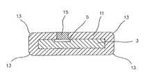
- FIG. 1illustrates a cross-sectional view of the integrated circuit coated with ultra-nanocrystalline diamond.
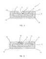
- FIG. 2depicts a cross-sectional view of an integrated circuit having a conductive portion of the ultra-nanocrystalline diamond coating.
- Ultra-nanocrystalline diamond (UNCD) thin film coatingsexhibit excellent mechanical, electrical, and electrochemical properties.
- Using a thin film coating deposition processsuch as that disclosed by Gruen and Krauss (U.S. Pat. No. 5,772,760) yields a coating that is inherently low in porosity, electrically non-conductive and biocompatible. Coatings as thin as 40 nm have demonstrated excellent hermetic properties.
- UNCD thin film coatingsare conformal when applied to complex or high aspect-ratio shapes. Since UNCD can be either patterned or selectively deposited, it also permits exposure of conductors and/or vias for interconnection with other components.
- electrical propertiescan be controlled by varying the deposition parameters, so as to make selected areas electrically conductivity,
- UNCD coating propertiesare not all present in any other single coating candidate for microchip packaging.
- Alternative coatingsare conventional chemical vapor deposited diamond thin films, diamond-like carbon, or SiC.
- UNCD coatingsexhibit:
- the UNCD coatingconsists primarily of phase pure randomly oriented diamond crystallites.
- UNCD coatingsare grown using a microwave plasma chemical vapor deposition technique involving a C 60 /Ar or CH 4 /Ar chemistry, which provides C 2 dimers as the main growth species that insert directly into the growing diamond lattice with a low energy barrier.
- the limited amount of atomic hydrogen in the plasmaleads to a very high re-nucleation rate ( ⁇ 10 11 cm ⁇ 2 sec ⁇ 1 ).
- the low activation energy for C 2 species incorporation into the growing filmyields UNCD films at temperatures as low as approximately 350° C. This temperature is very low compared to that required by many conventional coating processes, such as glass encapsulation or chemical vapor deposition.
- the present inventionuses the “chip” of an integrated circuit chip (which contains desired electronic circuitry) as the substrate for the stimulator or sensor, with the substrate and electronic circuitry being covered, as required, with a protective UNCD coating.
- Such approachadvantageously eliminates the need for a hermetically sealed lid or cover, and thus allows the stimulator or sensor to be made much thinner than has heretofore been possible.
- Integrated circuits that are implanted in a living bodybenefit from a UNCD coating that, in addition to biocompatibility, corrosion resistance, and hermeticity, can be patterned to expose the electrodes.
- a UNCD protective coatingcovers the substrate, hermetically sealing the circuitry under the coating. Electrodes associated with the implantable device may be selectively left uncovered by the protective coating, thereby allowing such electrodes to be exposed to body tissue and fluids when the stimulator is implanted in living tissue.
- the exposed electrodesmust be biocompatible.
- the electrodesmay be plated with a biocompatible metal, such as platinum or iridium or alloys of platinum and/or iridium.
- the UNCD coatingitself may be selectively doped so as to create electrically conductive integral portions of the coating that then act as electrodes, which in turn contact the living tissue.
- the UNCD film coatingmay be used as part of a hermetic chip level packaging process to isolate implantable electronic and passive components from chemical or electrolytic attack in the body.
- the UNCD coating on an integrated circuitis “conformal”, which means that the coating has a uniform thickness as the coating follows the contours of the device. Achieving a conformal coating on high aspect-ratio parts and around sharp corners on these devices is a particular challenge for thin films that are deposited by other means.
- an efficient integral capacitormay be formed between the stimulator and the living tissue by virtue of depositing a very thin layer of UNCD insulating film on the surface of the stimulator such that the thin film causes a capacitor to be formed.
- a capacitorcan advantageously be used to effectively stop current flow to the living tissue, thereby avoiding harm to the tissue that is caused by electrical current flow, while allowing the stimulating voltage signal to pass to the tissue.
- the inventionmay further be characterized as a method of making an implantable device that is either a stimulator or a sensor, where the device includes a substrate, electrodes formed on the substrate, and electrical circuitry formed on the substrate.
- Such methodincludes the steps of: (a) forming the electrical circuitry on the surface of a semiconductor substrate; (b) forming electrodes on the semiconductor substrate; (c) electrically interconnecting the electrodes with the electrical circuitry through the use of conductive paths that pass through or on the body of the semiconductor substrate; and (d) depositing a protective coating of UNCD over the entire surface area of the substrate, except for select areas of the electrodes, so that all but the exposed area of the electrodes is sealed and protected.
- FIG. 1provides a cross-sectional view of a preferred embodiment of a coated integrated circuit 1 . Due to the extremely thin film that is required, these figures are not drawn to scale.
- the integrated circuitis shown, where the silicon substrate 3 contains an electrode 5 on one surface that is connected by metal trace 7 to active circuitry 9 .
- the silicon substrate 3is coated with an ultra-nanocrystalline diamond 11 .
- the ultra-nanocrystalline diamond 11 coatinghas been removed in a selected portion to expose electrode 5 such that electrode 5 can contact living tissue directly when implanted.
- the ultra-nanocrystalline diamond 11has an approximately uniform thickness and has rounded corners 13 which are formed as part of the normal application process.
- the rounded corners 13are an advantage for implanted ultra-nanocrystalline diamond coated devices such as coated integrated circuit 1 because they eliminate sharp corners and sharp edges that might otherwise create stress concentrations in the living tissue which could damage the tissue.
- FIG. 2provides a cross-sectional view of an integrated circuit as in FIG. 1 , however, the normally electrically insulating ultra-nanocrystalline diamond 11 has been doped in a selected area to provide electrically conductive doped ultra-nanocrystalline diamond electrode 15 .
- This preferred configurationallows the ultra-nanocrystalline diamond 11 to be completely hermetically sealed around the silicon substrate 3 , thereby protecting the silicon substrate 3 and electrodes 5 from exposure to living tissue.
Landscapes
- Chemical & Material Sciences (AREA)
- Engineering & Computer Science (AREA)
- Inorganic Chemistry (AREA)
- General Chemical & Material Sciences (AREA)
- Chemical Kinetics & Catalysis (AREA)
- Materials Engineering (AREA)
- Mechanical Engineering (AREA)
- Metallurgy (AREA)
- Organic Chemistry (AREA)
- Health & Medical Sciences (AREA)
- Physics & Mathematics (AREA)
- Medicinal Chemistry (AREA)
- Public Health (AREA)
- Plasma & Fusion (AREA)
- Combustion & Propulsion (AREA)
- Pharmacology & Pharmacy (AREA)
- Epidemiology (AREA)
- Life Sciences & Earth Sciences (AREA)
- Animal Behavior & Ethology (AREA)
- General Health & Medical Sciences (AREA)
- Bioinformatics & Cheminformatics (AREA)
- Veterinary Medicine (AREA)
- Condensed Matter Physics & Semiconductors (AREA)
- General Physics & Mathematics (AREA)
- Computer Hardware Design (AREA)
- Microelectronics & Electronic Packaging (AREA)
- Power Engineering (AREA)
- Crystallography & Structural Chemistry (AREA)
- Electrotherapy Devices (AREA)
- Prostheses (AREA)
Abstract
Description
Claims (18)
Priority Applications (1)
| Application Number | Priority Date | Filing Date | Title |
|---|---|---|---|
| US13/474,003US8630720B2 (en) | 2001-02-28 | 2012-05-17 | Implantable device using ultra-nanocrystalline diamond |
Applications Claiming Priority (4)
| Application Number | Priority Date | Filing Date | Title |
|---|---|---|---|
| US27296201P | 2001-02-28 | 2001-02-28 | |
| US10/039,842US7127286B2 (en) | 2001-02-28 | 2001-10-26 | Implantable device using ultra-nanocrystalline diamond |
| US11/452,144US8214032B2 (en) | 2001-02-28 | 2006-06-12 | Implantable device using ultra-nanocrystalline diamond |
| US13/474,003US8630720B2 (en) | 2001-02-28 | 2012-05-17 | Implantable device using ultra-nanocrystalline diamond |
Related Parent Applications (1)
| Application Number | Title | Priority Date | Filing Date |
|---|---|---|---|
| US11/452,144DivisionUS8214032B2 (en) | 2001-02-28 | 2006-06-12 | Implantable device using ultra-nanocrystalline diamond |
Publications (2)
| Publication Number | Publication Date |
|---|---|
| US20120232371A1 US20120232371A1 (en) | 2012-09-13 |
| US8630720B2true US8630720B2 (en) | 2014-01-14 |
Family
ID=26716503
Family Applications (3)
| Application Number | Title | Priority Date | Filing Date |
|---|---|---|---|
| US10/039,842Expired - LifetimeUS7127286B2 (en) | 2001-02-28 | 2001-10-26 | Implantable device using ultra-nanocrystalline diamond |
| US11/452,144Expired - Fee RelatedUS8214032B2 (en) | 2001-02-28 | 2006-06-12 | Implantable device using ultra-nanocrystalline diamond |
| US13/474,003Expired - LifetimeUS8630720B2 (en) | 2001-02-28 | 2012-05-17 | Implantable device using ultra-nanocrystalline diamond |
Family Applications Before (2)
| Application Number | Title | Priority Date | Filing Date |
|---|---|---|---|
| US10/039,842Expired - LifetimeUS7127286B2 (en) | 2001-02-28 | 2001-10-26 | Implantable device using ultra-nanocrystalline diamond |
| US11/452,144Expired - Fee RelatedUS8214032B2 (en) | 2001-02-28 | 2006-06-12 | Implantable device using ultra-nanocrystalline diamond |
Country Status (3)
| Country | Link |
|---|---|
| US (3) | US7127286B2 (en) |
| AU (1) | AU2002252156A1 (en) |
| WO (1) | WO2002067770A2 (en) |
Families Citing this family (69)
| Publication number | Priority date | Publication date | Assignee | Title |
|---|---|---|---|---|
| US7069080B2 (en)* | 2000-09-18 | 2006-06-27 | Cameron Health, Inc. | Active housing and subcutaneous electrode cardioversion/defibrillating system |
| US6754528B2 (en) | 2001-11-21 | 2004-06-22 | Cameraon Health, Inc. | Apparatus and method of arrhythmia detection in a subcutaneous implantable cardioverter/defibrillator |
| US7039465B2 (en)* | 2000-09-18 | 2006-05-02 | Cameron Health, Inc. | Ceramics and/or other material insulated shell for active and non-active S-ICD can |
| US6721597B1 (en) | 2000-09-18 | 2004-04-13 | Cameron Health, Inc. | Subcutaneous only implantable cardioverter defibrillator and optional pacer |
| WO2003061537A1 (en)* | 2002-01-17 | 2003-07-31 | Masachusetts Eye And Ear Infirmary | Minimally invasive retinal prosthesis |
| US7162308B2 (en) | 2002-11-26 | 2007-01-09 | Wilson Greatbatch Technologies, Inc. | Nanotube coatings for implantable electrodes |
| US7190051B2 (en)* | 2003-01-17 | 2007-03-13 | Second Sight Medical Products, Inc. | Chip level hermetic and biocompatible electronics package using SOI wafers |
| CA2511908A1 (en)* | 2003-02-07 | 2004-08-26 | Optobionics Corporation | Implantable device using diamond-like carbon coating |
| US20040210141A1 (en)* | 2003-04-15 | 2004-10-21 | Miller David G. | Apparatus and method for dissipating heat produced by TEE probes |
| GB0318215D0 (en)* | 2003-08-04 | 2003-09-03 | Element Six Ltd | Diamond microelectrodes |
| US7263403B2 (en)* | 2004-05-25 | 2007-08-28 | Second Sight Medical Products, Inc. | Retinal prosthesis |
| US7297420B2 (en)* | 2004-08-27 | 2007-11-20 | Alfred E. Mann Foundation For Scientific Research | Material to prevent low temperature degradation of zirconia |
| US7718000B2 (en)* | 2005-10-11 | 2010-05-18 | Dimerond Technologies, Llc | Method and article of manufacture corresponding to a composite comprised of ultra nonacrystalline diamond, metal, and other nanocarbons useful for thermoelectric and other applications |
| US7572332B2 (en)* | 2005-10-11 | 2009-08-11 | Dimerond Technologies, Llc | Self-composite comprised of nanocrystalline diamond and a non-diamond component useful for thermoelectric applications |
| US20110005564A1 (en)* | 2005-10-11 | 2011-01-13 | Dimerond Technologies, Inc. | Method and Apparatus Pertaining to Nanoensembles Having Integral Variable Potential Junctions |
| EP1949437B2 (en)* | 2005-11-02 | 2021-08-04 | Second Sight Medical Products, Inc. | Implantable microelectronic device and method of manufacture |
| EP1883107A3 (en)* | 2006-07-07 | 2014-04-09 | Imec | Method for forming packaged microelectronic devices and devices thus obtained |
| US10426578B2 (en)* | 2006-10-16 | 2019-10-01 | Natural Dental Implants, Ag | Customized dental prosthesis for periodontal or osseointegration and related systems |
| US8602780B2 (en)* | 2006-10-16 | 2013-12-10 | Natural Dental Implants, Ag | Customized dental prosthesis for periodontal or osseointegration and related systems and methods |
| US9539062B2 (en) | 2006-10-16 | 2017-01-10 | Natural Dental Implants, Ag | Methods of designing and manufacturing customized dental prosthesis for periodontal or osseointegration and related systems |
| WO2009018172A2 (en) | 2007-07-27 | 2009-02-05 | Second Sight Medical Products | Implantable device for the brain |
| JP4395812B2 (en)* | 2008-02-27 | 2010-01-13 | 住友電気工業株式会社 | Nitride semiconductor wafer-processing method |
| EP2389101B1 (en)* | 2009-01-21 | 2020-11-18 | California Institute of Technology | Pocket-enabled chip assembly for implantable devices |
| US8718784B2 (en) | 2010-01-14 | 2014-05-06 | Nano-Retina, Inc. | Penetrating electrodes for retinal stimulation |
| US8442641B2 (en) | 2010-08-06 | 2013-05-14 | Nano-Retina, Inc. | Retinal prosthesis techniques |
| US8150526B2 (en) | 2009-02-09 | 2012-04-03 | Nano-Retina, Inc. | Retinal prosthesis |
| US8706243B2 (en) | 2009-02-09 | 2014-04-22 | Rainbow Medical Ltd. | Retinal prosthesis techniques |
| US8428740B2 (en) | 2010-08-06 | 2013-04-23 | Nano-Retina, Inc. | Retinal prosthesis techniques |
| US20100211146A1 (en)* | 2009-02-13 | 2010-08-19 | Strowbridge Ben W | Photoelectric activation of neurons using nanostructured semiconductors |
| US8552311B2 (en) | 2010-07-15 | 2013-10-08 | Advanced Bionics | Electrical feedthrough assembly |
| US8386047B2 (en) | 2010-07-15 | 2013-02-26 | Advanced Bionics | Implantable hermetic feedthrough |
| US8552554B2 (en) | 2010-08-12 | 2013-10-08 | Industrial Technology Research Institute | Heat dissipation structure for electronic device and fabrication method thereof |
| CN102403284B (en)* | 2010-09-15 | 2013-08-28 | 财团法人工业技术研究院 | Electronic package, heat dissipation structure for electronic device and manufacturing method thereof |
| US8571669B2 (en) | 2011-02-24 | 2013-10-29 | Nano-Retina, Inc. | Retinal prosthesis with efficient processing circuits |
| WO2012158834A1 (en) | 2011-05-16 | 2012-11-22 | Second Sight Medical Products, Inc. | Cortical interface with an electrode array divided into separate fingers and/or with a wireless transceiver |
| AU2012262665B2 (en)* | 2011-06-03 | 2017-02-02 | The University Of Melbourne | An electrode and a feedthrough for medical device applications |
| US8834757B2 (en) | 2011-09-30 | 2014-09-16 | Uchicago Argonne, Llc | Method for making particle/polymer composites and applications |
| CN104271165B (en) | 2012-04-30 | 2018-04-17 | 加州理工学院 | High number of pins implant device and its manufacture method |
| US10008443B2 (en) | 2012-04-30 | 2018-06-26 | California Institute Of Technology | Implant device |
| WO2014022885A1 (en)* | 2012-08-07 | 2014-02-13 | The University Of Melbourne | An intraocular device |
| US8829331B2 (en) | 2012-08-10 | 2014-09-09 | Dimerond Technologies Llc | Apparatus pertaining to the co-generation conversion of light into electricity |
| US8586999B1 (en) | 2012-08-10 | 2013-11-19 | Dimerond Technologies, Llc | Apparatus pertaining to a core of wide band-gap material having a graphene shell |
| US9040395B2 (en) | 2012-08-10 | 2015-05-26 | Dimerond Technologies, Llc | Apparatus pertaining to solar cells having nanowire titanium oxide cores and graphene exteriors and the co-generation conversion of light into electricity using such solar cells |
| EP2747158A1 (en)* | 2012-12-24 | 2014-06-25 | Université Pierre et Marie Curie (Paris 6) | Biocompatible carbon based electrode, its use and preparation process |
| US8874182B2 (en) | 2013-01-15 | 2014-10-28 | Google Inc. | Encapsulated electronics |
| US9370417B2 (en) | 2013-03-14 | 2016-06-21 | Nano-Retina, Inc. | Foveated retinal prosthesis |
| US9161712B2 (en)* | 2013-03-26 | 2015-10-20 | Google Inc. | Systems and methods for encapsulating electronics in a mountable device |
| WO2014205489A1 (en)* | 2013-06-25 | 2014-12-31 | The University Of Melbourne | A circuit board comprising an insulating diamond material |
| US9781842B2 (en) | 2013-08-05 | 2017-10-03 | California Institute Of Technology | Long-term packaging for the protection of implant electronics |
| US9474902B2 (en) | 2013-12-31 | 2016-10-25 | Nano Retina Ltd. | Wearable apparatus for delivery of power to a retinal prosthesis |
| US9331791B2 (en) | 2014-01-21 | 2016-05-03 | Nano Retina Ltd. | Transfer of power and data |
| CN104092662B (en)* | 2014-06-13 | 2018-02-02 | 小米科技有限责任公司 | The method, apparatus and routing device of operation are performed to the file on routing device |
| US10390720B2 (en) | 2014-07-17 | 2019-08-27 | Medtronic, Inc. | Leadless pacing system including sensing extension |
| US9399140B2 (en) | 2014-07-25 | 2016-07-26 | Medtronic, Inc. | Atrial contraction detection by a ventricular leadless pacing device for atrio-synchronous ventricular pacing |
| US9623234B2 (en) | 2014-11-11 | 2017-04-18 | Medtronic, Inc. | Leadless pacing device implantation |
| US9724519B2 (en) | 2014-11-11 | 2017-08-08 | Medtronic, Inc. | Ventricular leadless pacing device mode switching |
| TWI696448B (en)* | 2014-11-11 | 2020-06-21 | 芬蘭商腦部關懷公司 | An implantable electrode device and a method for manufacturing thereof |
| US9492668B2 (en) | 2014-11-11 | 2016-11-15 | Medtronic, Inc. | Mode switching by a ventricular leadless pacing device |
| US9492669B2 (en) | 2014-11-11 | 2016-11-15 | Medtronic, Inc. | Mode switching by a ventricular leadless pacing device |
| US9289612B1 (en) | 2014-12-11 | 2016-03-22 | Medtronic Inc. | Coordination of ventricular pacing in a leadless pacing system |
| WO2017171988A2 (en) | 2016-01-21 | 2017-10-05 | The Trustees Of Columbia University In The City Of New York | Micron-scale active complementary metal-oxide-semiconductor (cmos) optical tags |
| US11152232B2 (en) | 2016-05-26 | 2021-10-19 | Anand Deo | Frequency and phase controlled transducers and sensing |
| US9536758B1 (en) | 2016-05-26 | 2017-01-03 | Anand Deo | Time-varying frequency powered semiconductor substrate heat source |
| US11207527B2 (en) | 2016-07-06 | 2021-12-28 | Cardiac Pacemakers, Inc. | Method and system for determining an atrial contraction timing fiducial in a leadless cardiac pacemaker system |
| US10814133B2 (en)* | 2017-02-06 | 2020-10-27 | Zyvex Labs, Llc | Methods of fabricating an implantable device |
| FR3072565B1 (en)* | 2017-10-25 | 2019-10-11 | Chambre De Commerce Et D'industrie De Region Paris Ile De France | SOFT DIAMOND IMPLANT |
| WO2020247356A1 (en) | 2019-06-03 | 2020-12-10 | Dimerond Technologies, Llc | High efficiency graphene/wide band-gap semiconductor heterojunction solar cells |
| DE102019122888B4 (en) | 2019-08-27 | 2024-09-26 | Infineon Technologies Ag | Power semiconductor device and method |
| EP4417015A1 (en) | 2021-10-13 | 2024-08-21 | Deo, Anand | Conformable polymer for frequency-selectable heating locations |
Citations (13)
| Publication number | Priority date | Publication date | Assignee | Title |
|---|---|---|---|---|
| US4991582A (en) | 1989-09-22 | 1991-02-12 | Alfred E. Mann Foundation For Scientific Research | Hermetically sealed ceramic and metal package for electronic devices implantable in living bodies |
| US5432357A (en) | 1992-04-16 | 1995-07-11 | Kabushiki Kaisha Kobe Seiko Sho | Diamond film electronic devices |
| US5445859A (en) | 1992-08-14 | 1995-08-29 | Siemens Aktiengesellschaft | Multipolar electrode lead |
| US5660163A (en) | 1993-11-19 | 1997-08-26 | Alfred E. Mann Foundation For Scientific Research | Glucose sensor assembly |
| US5750926A (en) | 1995-08-16 | 1998-05-12 | Alfred E. Mann Foundation For Scientific Research | Hermetically sealed electrical feedthrough for use with implantable electronic devices |
| US5772760A (en) | 1991-11-25 | 1998-06-30 | The University Of Chicago | Method for the preparation of nanocrystalline diamond thin films |
| US5825078A (en) | 1992-09-23 | 1998-10-20 | Dow Corning Corporation | Hermetic protection for integrated circuits |
| US5999848A (en) | 1997-09-12 | 1999-12-07 | Alfred E. Mann Foundation | Daisy chainable sensors and stimulators for implantation in living tissue |
| US6043437A (en) | 1996-12-20 | 2000-03-28 | Alfred E. Mann Foundation | Alumina insulation for coating implantable components and other microminiature devices |
| US6081736A (en) | 1997-10-20 | 2000-06-27 | Alfred E. Mann Foundation | Implantable enzyme-based monitoring systems adapted for long term use |
| US6119028A (en) | 1997-10-20 | 2000-09-12 | Alfred E. Mann Foundation | Implantable enzyme-based monitoring systems having improved longevity due to improved exterior surfaces |
| US6162219A (en) | 1997-10-21 | 2000-12-19 | Akzo Nobel N.V. | Electrode |
| US6410877B1 (en) | 2000-01-30 | 2002-06-25 | Diamicron, Inc. | Methods for shaping and finishing prosthetic joint components including polycrystalline diamond compacts |
- 2001
- 2001-10-26USUS10/039,842patent/US7127286B2/ennot_activeExpired - Lifetime
- 2002
- 2002-02-26AUAU2002252156Apatent/AU2002252156A1/ennot_activeAbandoned
- 2002-02-26WOPCT/US2002/006180patent/WO2002067770A2/ennot_activeApplication Discontinuation
- 2006
- 2006-06-12USUS11/452,144patent/US8214032B2/ennot_activeExpired - Fee Related
- 2012
- 2012-05-17USUS13/474,003patent/US8630720B2/ennot_activeExpired - Lifetime
Patent Citations (13)
| Publication number | Priority date | Publication date | Assignee | Title |
|---|---|---|---|---|
| US4991582A (en) | 1989-09-22 | 1991-02-12 | Alfred E. Mann Foundation For Scientific Research | Hermetically sealed ceramic and metal package for electronic devices implantable in living bodies |
| US5772760A (en) | 1991-11-25 | 1998-06-30 | The University Of Chicago | Method for the preparation of nanocrystalline diamond thin films |
| US5432357A (en) | 1992-04-16 | 1995-07-11 | Kabushiki Kaisha Kobe Seiko Sho | Diamond film electronic devices |
| US5445859A (en) | 1992-08-14 | 1995-08-29 | Siemens Aktiengesellschaft | Multipolar electrode lead |
| US5825078A (en) | 1992-09-23 | 1998-10-20 | Dow Corning Corporation | Hermetic protection for integrated circuits |
| US5660163A (en) | 1993-11-19 | 1997-08-26 | Alfred E. Mann Foundation For Scientific Research | Glucose sensor assembly |
| US5750926A (en) | 1995-08-16 | 1998-05-12 | Alfred E. Mann Foundation For Scientific Research | Hermetically sealed electrical feedthrough for use with implantable electronic devices |
| US6043437A (en) | 1996-12-20 | 2000-03-28 | Alfred E. Mann Foundation | Alumina insulation for coating implantable components and other microminiature devices |
| US5999848A (en) | 1997-09-12 | 1999-12-07 | Alfred E. Mann Foundation | Daisy chainable sensors and stimulators for implantation in living tissue |
| US6081736A (en) | 1997-10-20 | 2000-06-27 | Alfred E. Mann Foundation | Implantable enzyme-based monitoring systems adapted for long term use |
| US6119028A (en) | 1997-10-20 | 2000-09-12 | Alfred E. Mann Foundation | Implantable enzyme-based monitoring systems having improved longevity due to improved exterior surfaces |
| US6162219A (en) | 1997-10-21 | 2000-12-19 | Akzo Nobel N.V. | Electrode |
| US6410877B1 (en) | 2000-01-30 | 2002-06-25 | Diamicron, Inc. | Methods for shaping and finishing prosthetic joint components including polycrystalline diamond compacts |
Non-Patent Citations (2)
| Title |
|---|
| D.M. Gruen, "Nanocrystalline Diamond Films" Annu. Rev. Mater. Sci., 29 211-59 (1999). |
| D.M. Gruen, et al. "Buckyball Microwave Plasmas: Fragmentation and Diamond Film Growth", J. Appl. Phys., 75(3) 1758-63 (1994). |
Also Published As
| Publication number | Publication date |
|---|---|
| WO2002067770A3 (en) | 2002-12-12 |
| US20020120296A1 (en) | 2002-08-29 |
| US7127286B2 (en) | 2006-10-24 |
| US20120232371A1 (en) | 2012-09-13 |
| WO2002067770A2 (en) | 2002-09-06 |
| AU2002252156A1 (en) | 2002-09-12 |
| US20060235475A1 (en) | 2006-10-19 |
| WO2002067770B1 (en) | 2003-08-21 |
| US8214032B2 (en) | 2012-07-03 |
Similar Documents
| Publication | Publication Date | Title |
|---|---|---|
| US8630720B2 (en) | Implantable device using ultra-nanocrystalline diamond | |
| US10589102B2 (en) | Micro-miniature implantable coated device | |
| JP5254622B2 (en) | Implantable hermetic sealed structure | |
| US7709961B2 (en) | Implantable microelectronic device and method of manufacture | |
| JP5258245B2 (en) | Implantable biocompatible components with built-in active sensors, microelectromechanical systems or integrated circuits for measuring physiological parameters | |
| CN105324101B (en) | Long-term packaging for protection of implantable electronic devices | |
| US20100016928A1 (en) | Void-free implantable hermetically sealed structures | |
| WO1999065388A1 (en) | Substrate sensor | |
| WO2008134615A2 (en) | Metallization with tailorable coefficient of thermal expansion | |
| US20040220667A1 (en) | Implantable device using diamond-like carbon coating | |
| US8461681B2 (en) | Layered structure for corrosion resistant interconnect contacts | |
| US6614095B1 (en) | Diamond component with rear side contact and a method for the production thereof | |
| KR100463248B1 (en) | Flexible electrode equipment for cochlear implant |
Legal Events
| Date | Code | Title | Description |
|---|---|---|---|
| AS | Assignment | Owner name:SECOND SIGHT MEDICAL PRODUCTS, INC., CALIFORNIA Free format text:MERGER;ASSIGNOR:SECOND SIGHT, LLC;REEL/FRAME:028226/0722 Effective date:20030731 Owner name:SECOND SIGHT, LLC, CALIFORNIA Free format text:ASSIGNMENT OF ASSIGNORS INTEREST;ASSIGNORS:MECH, BRIAN V;GREENBERG, ROBERT J;REEL/FRAME:028226/0677 Effective date:20011026 | |
| STCF | Information on status: patent grant | Free format text:PATENTED CASE | |
| FPAY | Fee payment | Year of fee payment:4 | |
| MAFP | Maintenance fee payment | Free format text:PAYMENT OF MAINTENANCE FEE, 8TH YR, SMALL ENTITY (ORIGINAL EVENT CODE: M2552); ENTITY STATUS OF PATENT OWNER: SMALL ENTITY Year of fee payment:8 | |
| AS | Assignment | Owner name:CORTIGENT, INC., CALIFORNIA Free format text:ASSIGNMENT OF ASSIGNORS INTEREST;ASSIGNOR:VIVANI MEDICAL, INC.;REEL/FRAME:062588/0685 Effective date:20221228 | |
| FEPP | Fee payment procedure | Free format text:MAINTENANCE FEE REMINDER MAILED (ORIGINAL EVENT CODE: REM.); ENTITY STATUS OF PATENT OWNER: SMALL ENTITY |