US8630054B2 - Systems and methods for data throttling during disk drive power down - Google Patents
Systems and methods for data throttling during disk drive power downDownload PDFInfo
- Publication number
- US8630054B2 US8630054B2US13/239,176US201113239176AUS8630054B2US 8630054 B2US8630054 B2US 8630054B2US 201113239176 AUS201113239176 AUS 201113239176AUS 8630054 B2US8630054 B2US 8630054B2
- Authority
- US
- United States
- Prior art keywords
- controller
- supply voltage
- internal supply
- storage system
- data storage
- Prior art date
- Legal status (The legal status is an assumption and is not a legal conclusion. Google has not performed a legal analysis and makes no representation as to the accuracy of the status listed.)
- Expired - Fee Related, expires
Links
Images


Classifications
- G—PHYSICS
- G06—COMPUTING OR CALCULATING; COUNTING
- G06F—ELECTRIC DIGITAL DATA PROCESSING
- G06F11/00—Error detection; Error correction; Monitoring
- G06F11/07—Responding to the occurrence of a fault, e.g. fault tolerance
- G06F11/0703—Error or fault processing not based on redundancy, i.e. by taking additional measures to deal with the error or fault not making use of redundancy in operation, in hardware, or in data representation
- G06F11/0706—Error or fault processing not based on redundancy, i.e. by taking additional measures to deal with the error or fault not making use of redundancy in operation, in hardware, or in data representation the processing taking place on a specific hardware platform or in a specific software environment
- G06F11/0727—Error or fault processing not based on redundancy, i.e. by taking additional measures to deal with the error or fault not making use of redundancy in operation, in hardware, or in data representation the processing taking place on a specific hardware platform or in a specific software environment in a storage system, e.g. in a DASD or network based storage system
- G—PHYSICS
- G11—INFORMATION STORAGE
- G11B—INFORMATION STORAGE BASED ON RELATIVE MOVEMENT BETWEEN RECORD CARRIER AND TRANSDUCER
- G11B19/00—Driving, starting, stopping record carriers not specifically of filamentary or web form, or of supports therefor; Control thereof; Control of operating function ; Driving both disc and head
- G11B19/02—Control of operating function, e.g. switching from recording to reproducing
- G11B19/04—Arrangements for preventing, inhibiting, or warning against double recording on the same blank or against other recording or reproducing malfunctions
- G11B19/041—Detection or prevention of read or write errors
- G—PHYSICS
- G11—INFORMATION STORAGE
- G11B—INFORMATION STORAGE BASED ON RELATIVE MOVEMENT BETWEEN RECORD CARRIER AND TRANSDUCER
- G11B19/00—Driving, starting, stopping record carriers not specifically of filamentary or web form, or of supports therefor; Control thereof; Control of operating function ; Driving both disc and head
- G11B19/20—Driving; Starting; Stopping; Control thereof
- G11B19/2063—Spindle motor power-down sequences
- G11B19/2081—Spindle motor power-down sequences emergency power-down
- G—PHYSICS
- G11—INFORMATION STORAGE
- G11B—INFORMATION STORAGE BASED ON RELATIVE MOVEMENT BETWEEN RECORD CARRIER AND TRANSDUCER
- G11B2220/00—Record carriers by type
- G11B2220/20—Disc-shaped record carriers
- G11B2220/25—Disc-shaped record carriers characterised in that the disc is based on a specific recording technology
- G11B2220/2508—Magnetic discs
- G11B2220/2516—Hard disks
- G—PHYSICS
- G11—INFORMATION STORAGE
- G11B—INFORMATION STORAGE BASED ON RELATIVE MOVEMENT BETWEEN RECORD CARRIER AND TRANSDUCER
- G11B2220/00—Record carriers by type
- G11B2220/40—Combinations of multiple record carriers
- G11B2220/45—Hierarchical combination of record carriers, e.g. HDD for fast access, optical discs for long term storage or tapes for backup
- G—PHYSICS
- G11—INFORMATION STORAGE
- G11B—INFORMATION STORAGE BASED ON RELATIVE MOVEMENT BETWEEN RECORD CARRIER AND TRANSDUCER
- G11B2220/00—Record carriers by type
- G11B2220/60—Solid state media
- G11B2220/63—Solid state media wherein solid state memory is used as a supplementary storage medium to store auxiliary data for detecting or correcting errors on a main storage medium
Definitions
- the present inventionrelates to disk drives and data storage systems for computer systems. More particularly, the present invention relates to systems and methods for enhancing power management during a spin down mode in which power is extracted from the spindle of a disk.
- Disk drivestypically comprise a disk and a head connected to a distal end of an actuator arm which is rotated about a pivot by a voice coil motor (VCM) to position the head radially over the disk.
- VCMvoice coil motor
- the diskcomprises a plurality of radially spaced, concentric tracks for recording user data sectors and embedded servo sectors.
- the embedded servo sectorscomprise head positioning information (e.g., a track address) which is read by the head and processed by a servo controller to control the velocity of the actuator arm as it seeks from track to track.
- a braking torqueis applied to the spindle motor to stop it from rotating as quickly as possible in order to minimize head wear.
- the internal supply voltageneeds to be managed carefully to support the above described head parking function, as well as any operation the disk may need to perform in such a situation.
- FIG. 1shows a disk drive/data storage system according to some embodiments of the invention.
- FIG. 2Ashows another disk drive/data storage system according to some embodiments of the invention.
- FIG. 2Billustrates the format of a servo sector according to some embodiments of the invention.
- FIG. 3illustrates a power down sequence according to some embodiments of the invention.
- FIG. 4shows spin down circuitry according to some embodiments of the invention.
- FIG. 5shows demand regulation circuitry according to some embodiments of the invention.
- FIG. 6shows demand regulation circuitry with prioritization according to some embodiments of the invention.
- FIGS. 7A-7Dshow various arrangement of logic load according to some embodiments of the invention.
- FIGS. 8A-8Cillustrate load staggering according to some embodiments of the invention.
- FIGS. 9A-9Cillustrate effects of load staggering according to some embodiments of the invention.
- FIG. 10illustrates power transfer improvements according to some embodiments of the invention.
- Embodiments of the data storage system provided hereinare configured to perform improved energy or power transfer mechanisms during power down, loss, or failure.
- diskand “head” are used throughout this disclosure, those skilled in art would appreciate that multiple disks (or platters) and heads can be used in some embodiments.
- Various types of data storage systems/disk drivescan include non-volatile memory (NVM) (e.g., solid-state memory) for storing data in the event of a power interruption. Storing data in non-volatile memory in the event of a power failure can improve overall performance (e.g., by enabling use of a larger write cache), and/or may be necessary to prevent loss of data during power failure.
- hybrid drivesmay include solid-state non-volatile memory for performing boosting functions where frequently accessed data is stored in the solid-state non-volatile memory instead of, or in addition to, the hard disk to increase performance.
- a data storage system/disk drive that includes a disk and non-volatile memorymay need to perform at least two tasks during power failure: park the head and program data (e.g., user data, system data, or both) into non-volatile memory.
- program datae.g., user data, system data, or both
- non-volatile memorye.g., solid-state memory
- programmingcannot tolerate power interruptions because data can become corrupted. Programming can take up to 1-2 milliseconds, during which power cannot be interrupted.
- voltage generated using BEMFis also used for parking the head, and thus must be managed to ensure head parking and programming functions are completed in an efficient manner.
- Some embodiments of the inventionuse BEMF generated power more efficiently in order to provide sufficient power to park the head and program as much data as possible into the non-volatile memory during a power failure.
- a demand regulation circuitis used to regulate loads connected to an internal supply voltage generated from the BEMF.
- the internal supply voltageis supplied to a controller for programming data to non-volatile memory during a power interruption
- the demand regulation circuitis used to selectively cause the controller to adjust a rate of data programming of the non-volatile memory in order to reduce its load on the internal supply voltage.
- the demand regulation circuitmay assert a discrete digital throttle signal to the controller upon detecting that the internal supply voltage is below a certain threshold level.
- the throttle signalmay be asserted directly to the logic circuitry coupled with the solid-state non-volatile memory to regulate a rate of data programming.
- the rate of data programmingmay be throttled and/or programming cycles may be lengthened.
- the controllerin response to the assertion of the discrete digital throttle signal, the controller may be configured to stagger programming cycle start times during programming of multiple solid-state memory devices in the data storage system/disk drive. Data throttling may enable the use of a smaller sized capacitor associated with one or more loads (including the controller).
- the controller and/or the logic circuitry coupled with the solid-state non-volatile memorymay take several types of action (alone or in combination) when the throttle signal is asserted. For example, it may: (1) not start any new drive operations (such as non-volatile memory programming cycles) and allow current drive operations to finish, (2) modify the start of new drive operations in such a manner as to match the load to the available power, and (3) infer the load caused by various drive operations from observations of the internal supply voltage rail.
- multiple other loadssuch as a voice coil motor (VCM), pre-amplification, and other functions are also supplied power from the same internal supply voltage generated from the BEMF voltage.
- VCMvoice coil motor
- pre-amplificationpre-amplification
- other functionsare also supplied power from the same internal supply voltage generated from the BEMF voltage.
- Separate drive electronicsmay be used to control each load.
- the demand regulation circuitmay be adapted to provide load prioritization.
- load prioritycan be established in two ways: by tiered threshold levels or by logic control.
- logic controlcan correspond to throttling a lower priority load, while not throttling a higher priority load.
- a second lower threshold voltagecan be used for the VCM.
- controller and/or solid-state memory logicmay be shut down first, allowing more of the total available power to be used by VCM. After VCM transient load (e.g., moving the head) is reduced, the internal supply voltage rises again, and the logic may be turned on when a higher threshold voltage is reached.
- the logic controlmay include timing functions, and the logic control may produce a better load distribution and a smaller circuit.
- the loadscan be isolated and provided with their own energy reservoirs, which when dissipated cause a smooth rejoinder to the internal supply voltage.
- One embodiment of the inventionis directed to a data storage system comprising, a disk, a head, a spindle motor for rotating the disk, the spindle motor comprising a plurality of windings and a rotor rotatable at a variable spin rate wherein the rotor generates a back EMF (BEMF) voltage across the windings proportional to the spin rate of the rotor, a plurality of switching elements coupled to the windings; switch control logic for generating switch control signals applied to the switching elements for generating an internal supply voltage from the BEMF during a spin down mode, the internal supply voltage enabling one or more components in the data storage system to perform an operation in an event of a power interruption to the data storage system; and a demand regulation circuit for regulating the amount power supplied to one or more of the above described components for performing power down related functions to increase an amount of time the spindle motor remains spinning in the event of a power interruption.
- one such componentis a controller for controlling data operations to non-volatile memory.
- Another embodiment of the inventionis directed to a method for managing power in a data storage system during a spin down mode, the data storage system comprising: a disk, a head, a spindle motor for rotating the disk, the spindle motor comprising a plurality of windings and a rotor rotatable at a variable spin rate wherein the rotor generates a back EMF (BEMF) voltage across the windings proportional to the spin rate of the rotor; a plurality of switching elements coupled to the windings; and switch control logic for generating switch control signals applied to the switching elements for generating an internal supply voltage from the BEMF during a spin down mode, the internal supply voltage enabling one or more component in the data storage system to perform an operation in an event of a power interruption to the data storage system, the method comprising: asserting a demand limit signal to the one or more component in response to detecting that the internal supply voltage falls below a predetermined level, thereby increasing an amount of time the spindle motor remains spinning in the event of
- the use of a demand regulation circuit to regulate data programming rate in the solid-state non-volatile memory and/or other disk drive functionsis beneficial in the following aspects.
- the energy transfer from the spindle motor to the disk drive electronicsis more efficient because of a reduction in time duration during which a peak current is drawn from the spindle motor.
- Enhanced efficiencyincreases the total spin down time and allows for an increased total amount of data that can be stored in the non-volatile memory. This results in a larger feasible cache size and better drive performance.
- the techniquenaturally allows power trading between power down operations and systems. Specifically, additional improvements in the VCM park circuit power efficiency directly result in more available power for the digital logic in the controller.
- the minimum cache size protected by non-volatile memory with the power down systemcan be increased with each improvement in the parking power down system.
- this arrangementlargely compensates for the large variations in peak power availability found in large production volumes of hard disks and obviates the need to directly calculate load demands, which can be non-linear.
- FIG. 1illustrates a disk drive 100 according to some embodiments of the invention.
- Disk drive 100comprises a disk 102 , a head 104 actuated radially over the disk 102 , and a spindle motor 106 for rotating the disk 102 .
- the spindle motor 106comprises a plurality of windings 108 and a rotor rotatable at a variable spin rate, wherein the rotor generates a back EMF (BEMF) voltage across the windings 108 proportional to the spin rate of the rotor.
- BEMF voltageis used to generate an internal supply voltage Vpwr 112 for parking the head 104 and for performing other operations.
- the internal supply voltage Vpwr 112is applied to a voice coil motor (VCM) 110 in order to park the head 104 during the spin down mode.
- VCMvoice coil motor
- the internal supply voltage Vpwr 112is used to park the head 104 in response to a power failure or power down condition.
- the internal supply voltage Vpwr 112is used to park the head 104 during a normal spin down mode, for example, when the disk drive is placed in an idle mode.
- FIG. 2illustrates a disk drive 200 according to some embodiments of the invention.
- Disk drive 200comprises a disk 102 , an actuator arm 4 , a head 104 connected to a distal end of the actuator arm 4 , and a ramp 8 near an outer periphery of the disk 102 .
- the disk 102comprises a plurality of data tracks 10 and a first and second set of reserved tracks 12 A and 12 B, wherein the first set of reserved tracks 12 A are located at a first radial location, and the second set of reserved tracks 12 B are located at a second radial location different than the first radial location.
- the disk drivefurther comprises control circuitry 14 . In some embodiments, when a power failure is detected the head is unloaded onto the ramp 8 .
- the disk 102comprises a plurality of servo sectors 24 0 - 24 N that define the plurality of data tracks 10 and the sets of reserved tracks 12 A and 12 B.
- the control circuitry 14processes the read signal to demodulate the servo sectors 24 0 - 24 N into a position error signal (PES).
- PESposition error signal
- the PESis filtered with a suitable compensation filter to generate a control signal 26 applied to a voice coil motor (VCM) 110 which rotates the actuator arm 4 about a pivot in order to position the head 104 radially over the disk 102 in a direction that reduces the PES.
- VCMvoice coil motor
- the servo sectors 24 0 - 24 Nmay comprise any suitable position information, and in some embodiments, as is shown in FIG.
- each servo sectorcomprises a preamble 30 for synchronizing gain control and timing recovery, a sync mark 32 for synchronizing to a data field 34 comprising coarse head positioning information such as a track number, and servo bursts 36 which provide fine head positioning information.
- the coarse head position informationis processed to position a head over a target track during a seek operation, and the servo bursts 36 are processed to maintain the head over a centerline of the target track while writing or reading data during a tracking operation.
- a disk driveperforms several operations during power down, including parking the head and programming data into non-volatile memory (e.g., to save any data stored in a volatile memory cache).
- data programmed into non-volatile memorycan include user and system data.
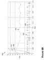
- FIG. 3illustrates a power down sequence 300 according to some embodiments of the invention.
- the x-axisrepresents time in seconds and the y-axis represents units for the various illustrated lines, such as volts, degrees, inches per second, and miliamperes (scaled).
- Line 310reflects an internal supply voltage Vpwr (generated from BEMF), which is shown as degrading from about 15V to about 10V. Those skilled in art would appreciate that these depicted voltage levels are for illustrative purposes only and that other voltage levels/ranges may be used. In this example, the voltage levels correspond to desktop disk drives, which typically require a 12V power supply. Those skilled in the art would appreciate that some embodiments can represent portable or mobile disk drives, which typically require a 5V power supply.
- Line 320reflects the rotational speed of the spindle motor, which is shown to slow down from about 10 kRPM (revolutions per minute) to about 8 kRPM.
- Line 330represents the current drawn from a secondary switching regulator by a load after a switching supply (which transforms small currents at high voltages to larger currents at lower voltages) has converted Vpwr voltage from low current, high voltage signal to high current, low voltage signal. That is, current drawn from the internal supply depends on the voltage of the supply.
- Region 332represents the current drawn by non-volatile memory during programming, which is larger than current drawn during idle periods.
- Line 340represents head velocity. As is illustrated, the head is being moved into a parked position, and in region 342 the head is parked on a ramp.
- Line 350represents the head position. When the head is being parked, it is moved to a zero degree position 352 , which corresponds to a ramp contact.
- Line 360represents ramp contact.
- Region 362reflects the head moving into a latched position on the ramp.
- Line 370represents the current drawn by VCM.
- Line 380represents the same current as line 330 , but the current represented by line 380 is drawn from the internal supply.
- FIG. 4illustrates spin down circuitry 400 that generates the internal supply voltage according to some embodiments of the invention.
- a spindle motor 420comprises a plurality of windings 422 , 424 , and 426 , wherein a rotor generates BEMF voltage across the windings proportional to the spin rate of the rotor.
- the spindle motor illustrated in FIG. 4is a three phase motor comprising three windings. BEMF voltage in each of the windings will be positioned 120 degrees out of phase with respect to the other windings.
- the phase of BEMF voltage signal in winding 422can be 120 degrees
- the phase of BEMF voltage signal in winding 424can be 240 degrees
- the phase of BEMF voltage signal in winding 426can be 0 degrees.
- a three-phase configurationis shown, those skilled in the art would appreciate that other number of phases can be used as well in other embodiments.
- a plurality of switching elements 408are coupled to the windings, and switch control logic 402 , 404 , and 406 generates switch control signals applied to the switching elements for commutating the spindle motor during normal operation and for generating an internal supply voltage Vpwr 440 from the BEMF during the spin down mode.
- a rectifier circuit 410 for rectifying the generated voltageis coupled to the windings 422 , 424 , and 426 .
- Vpwr 440can be generated using synchronous rectification.
- Commutation logic 404turns on the switches 408 , which creates a path between the windings and ground. With simple rectification, the most positive phase of BEMF voltage in the windings will drive the Vpwr terminal, while the most negative phase will drive the ground terminal.
- the diodes in the rectifier circuit 410rectify the AC voltage. This circuit is equivalent to a transformer circuit. Its impedance is comprised of the impedance of windings inductors and of the switching transistors. FIG.
- synchronous rectificationincludes both simple rectification and/or synchronous switching.
- Vpwr 440can be generated using “boost braking,” as is described in U.S. Pat. Nos. 6,459,361, 6,549,359, and 6,577,465. The disclosure of each of these patents is hereby incorporated by reference in its entirety.
- a periodic signalis generated by a timer 402 for periodically shorting the windings 422 , 424 , and 426 during the spin down mode in order to boost the internal supply voltage Vpwr 440 , wherein shorting the windings applies a braking torque to the spindle motor.
- a currentbuilds up in the inductance of the windings and energy is stored in the inductors.
- Vpwr 440will rise above the BEMF voltage. In some embodiments, Vpwr 440 will rise to whatever voltage is needed to drive the currents in the inductors toward zero.
- BEMF voltagecan be used to charge a capacitor or network of capacitors, and the stored energy can be used to power a logic load and/or other components in the disk drive/data storage system, as is explained below.
- a conflictmay arise when the VCM demands more current (which is supplied by the Vpwr terminal) to park the head in the spin down mode during power down. There may not be enough power available to program data in the non-volatile memory. However, non-volatile memory programming may not tolerate power interruptions because data could become corrupted.
- FIG. 5illustrates demand regulation circuitry 500 according to some embodiments.
- the internal supply voltage Vpwr 440is generated from the BEMF during spin down.
- Vref 510represents a voltage threshold selected for an optimal power transfer.
- Vrefcan be higher for desktop disk drives and lower for portable disk drives.
- a comparator 520compares voltage Vpwr 440 with the Vref 510 threshold. When voltage Vpwr 440 falls below the Vref 510 threshold, the comparator 520 can generate a throttle signal 530 (e.g., discrete digital signal) used for informing the logic load (which may cause it to take action to reduce its load partially or completely) and allowing Vpwr 440 voltage to recover.
- the logic loadcan be reduced in various ways. For example, where the logic load is in a controller for controlling data operations to non-volatile memory, the controller may elect to slow down its clock speed, shut off the clock, reduce its regulated voltage, or otherwise reduce its power usage.
- asserting the throttle signal 530can prevent the start of a new program cycle, but should not interrupt a programming cycle already in progress.
- faster tiers of non-volatile memorycan be selected or reserved to store data during power down.
- parts or areas of non-volatile memorycan be reserved for storing data during power down. Since there may be limited time (dictated by the energy available) to preserve data in a power down situation, certain portions of the memory with faster programming times may be reserved for this purpose. Such parts of the non-volatile memory can be optimized for programming beforehand (e.g., during normal operation).
- a capacitor Cpwr 550can be used to compensate for a ripple (i.e., drop) in voltage Vpwr 440 .
- energy stored in the capacitor Cpwr 550can be used to provide power to the load.
- the capacitor Cpwr 550should be able to store enough energy (e.g., be large enough) to compensate for the ripple in Vpwr 440 .
- the capacitor Cpwrcan be used to power the load when the throttle signal 530 has been asserted.
- the capacitor Cpwr 550can provide power to complete a programming cycle that is already in progress.
- more than one loadmay be used, and one capacitor (or several) may be coupled with the loads.
- the logic load represented as block 560 in FIG. 5can comprise one or more of: system on chip (SoC) module 564 (e.g., to implement controller functions), SoC regulators module 562 for regulating power distributed to various logic components of the load, DRAM data buffer 566 (which can store data that should be programmed), and non-volatile memory module 568 .
- SoCsystem on chip
- DRAM data buffer 566which can store data that should be programmed
- non-volatile memory module 568can comprise single or multiple NVM die of various types, such as NAND flash die, NOR flash die, etc.
- the SoC regulators module 562can be part of the SoC module 564 .
- the logic loadcan be in a variety of configurations.
- the VCM amplifier 540when the throttle signal 530 has been asserted, can still provide power to the VCM for parking the head. In some embodiments, VCM amplifier 540 can shut off power to VCM when the throttle signal 530 has been asserted. This is further described in the above referenced U.S. Pat. Nos. 6,459,361, 6,549,359, and 6,577,465.
- load prioritycan be used to provide optimal power transfer and usage across several loads.
- several voltage thresholds Vref 1 610 and Vref 2 620can be used to prioritize between different loads.
- threshold Vref 2 620can correspond to a voltage threshold provided to a comparator 630 for generating a throttle signal 660 (e.g., discrete digital signal) for causing the logic load 560 to reduce its power use partially or completely (e.g., causing it to temporarily inhibit operation). This conserves the internal supply voltage for use by the VCM.
- a throttle signal 660e.g., discrete digital signal
- Threshold Vref 1 610can correspond to a voltage threshold provided to a comparator 640 , which may provide a demand limit signal 650 as an indication to the VCM (e.g., for temporarily turning off or on). In some embodiments, more than two thresholds levels can be tiered to throttle different loads, such as VCM, controller, different types of non-volatile memory, etc.
- Threshold Vref 2 620can be higher, lower, or same as threshold Vref 1 610 . In system 600 , threshold Vref 2 can be higher than threshold Vref 1 because parking the head has higher priority than programming data.
- the general conceptcan be expanded to any N number of loads (e.g., 3 to 10 or more) with one or more of the N loads associated with a different Vref value.
- Ne.g. 3 to 10 or more
- four loadsmay be present with two loads sharing a Vref 1 , a third load associated with a Vref 2 , and a fourth load associated with a Vref 3 .
- loadscan be provided with separate power reservoirs (e.g., capacitors).
- Demand regulationcan optimize the transfer of power, which in turn can increase data throughput and allow more data to be stored in the non-volatile memory. Accordingly, larger volatile memory cache can be used in the disk drive since more data from the cache can be written in case of power loss.
- logic loadcan be within one or more of: a separate data buffer 710 A, SoC module 720 A, and non-volatile memory module 730 A.
- Throttle signal 740 Ae.g., discrete digital signal
- the demand regulatorcan be used to initiate throttling functions in the logic within at least SoC module 720 A, which may in turn control programming of the non-volatile memory module 730 A (e.g., to store any data in the data buffer 710 A or a cache into non-volatile memory in the event of a power interruption).
- the non-volatile memory modulemay include the flash memory portion of the drive.
- a component or circuitmay be described as being “throttled” below and throughout the disclosure, the precise functions performed by the corresponding component or circuit in response to a “throttle” signal may vary to reduce or eliminate power usage.
- the data programming ratesmay be reduced with delays between cycles lengthened, or programming on multiple solid-state memory devices may be staggered. Additional examples are provided in FIGS. 8A-C and 9 A-C.
- certain actionsmay be delayed or a mode of operation may be altered.
- the throttle signal 740 Acan be provided to the non-volatile memory module 730 A to achieve throttling independent of the SoC.
- non-volatile memory module 730 Acan comprise a controller that can be throttled separately from the SoC module 720 A.
- non-volatile memory modulecan comprise a bridge device, which is described in a co-pending patent application Ser. No. 13/226,393, entitled “Systems and Methods for an Enhanced Controller Architecture in Data Storage Systems,” filed Sep. 6, 2011, the disclosure of which is hereby incorporated by reference in its entirety.
- the bridge devicecan be throttled separately in some embodiments.
- only the non-volatile memory module 730 A (and not the SoC module 720 A)can be throttled.
- the SoC module 720 Bcan comprise a throttle module 724 B, which is implemented in hardware in one embodiment.
- the throttle module 724 Bmonitors Vpwr rail and generates an indication (e.g., a signal) when Vpwr falls below a threshold.
- the SoC module 720 Bcan then send a command (e.g., a THROTTLE_OPERATION command) to the non-volatile memory module to configure it to operate in a low power mode.
- the commandcan be transmitted over a data bus or dedicated command bus.
- the bridge device of the non-volatile memory module 730 Bin response to receiving the THROTTLE_OPERATION command, will not start new programming operations. This is further described in a co-pending patent application Ser. No. 13/226,393, entitled “Systems and Methods for an Enhanced Controller Architecture in Data Storage Systems,” filed Sep. 6, 2011.
- the throttle module 724 Bcan send another command (e.g., NORMAL_OPERATION) to configure the non-volatile memory module to operate in a normal mode.
- the throttle module 724 Bcan be a separate module, apart from the SoC module 720 B.
- the controllercan be integrated with the non-volatile memory module 750 C.
- Programming datacan be stored in a buffer 710 C.
- the non-volatile memory module 750 Ccan be throttled by a throttle signal 740 C (e.g., discrete digital signal).
- a throttle signal 740 Ce.g., discrete digital signal
- a SoC modulemay have already been powered off.
- the module 750 Ccan instead comprise the above described throttle module.
- the buffer 762 Dcan be integrated with the non-volatile memory module 760 D.
- the module 760 Dcan also comprise a controller and NVM module 764 D, which can be throttled by a throttle signal 740 D (e.g., discrete digital signal).
- a throttle signal 740 De.g., discrete digital signal
- the module 760 Dcan instead comprise the above described throttle module.
- power transfercan be further optimized by staggering programming cycles of multiple non-volatile memory modules.
- N non-volatile memory modulescan be programmed using a round robin scheme in order to achieve load balancing (e.g., to even out the load).
- Other scheduling methodscan be used to program the non-volatile memory, including weighted round robin, first in first out (FIFO) queuing, fair queuing, weighted fair queuing, etc.
- a programming sequencecan be divided into N cycles or time periods.
- the periodscan be of equal lengths (e.g., 1/N) or of different lengths. If at the end of each period (e.g., period Y/N) the throttle signal is not asserted, the next non-volatile memory module (e.g., module Y) can be programmed. However, if the throttle signal is asserted, the system will wait for the throttle signal to be deactivated before starting the next programming cycle. As previously started programming cycles are completed, the aggregate load connected to the Vpwr terminal will be reduced gradually. Vpwr voltage will recover because the loads stop drawing power and the BEMF voltage generated by the spindle motor replenishes the Vpwr rail.
- FIG. 8Aillustrates operation of the system 800 A in which programming cycle sequences 810 A, 820 A, 830 A, and 840 A are not staggered.
- each boxrepresents a programming cycle, and active cycles are illustrated in plain boxes while inactive (not-performed) cycles are illustrated in striped boxes.
- the programming cycle sequences 810 A, 820 A, 830 A, and 840 Acan correspond to programming cycle sequences of different non-volatile memory modules. As is illustrated, when the throttle signal 850 A is asserted at time 860 A, all four non-volatile memory modules are being programmed. In some embodiments, programming cycles that are already in progress must be completed before powering off the non-volatile memory.
- FIG. 8Billustrates operation of the system 800 B in which programming cycle sequences 810 B, 820 B, 830 B, and 840 B are staggered. Active cycles are illustrated in plain boxes while inactive (not-performed) cycles are illustrated in striped boxes. As is illustrated, when the throttle signal 850 B is asserted at time 860 B, three programming cycles from sequences 810 B, 820 B, and 830 B are already in progress. The system 800 B will complete these cycles, but will not start the scheduled programming cycle from sequence 840 B until the throttle signal becomes deasserted at time 862 B. Load balancing allows Vpwr voltage to recover faster than in the system 800 A of FIG. 8A .
- the controllercan adjust the timing of programming cycles in accordance with the throttle signal 850 C.
- the throttle signal 850 Cis deasserted at time 862 C, the programming cycle from the sequence 810 C, which was delayed due to throttling, can be started immediately.
- FIGS. 9A-9Cillustrate the effects of load staggering according to some embodiments of the invention.
- FIG. 9Aillustrates the performance of a system 900 A in which programming cycles are not staggered (e.g., as is done in the system 800 A of FIG. 8A ).
- Line 910 Arepresents Vpwr voltage
- line 920 Arepresents programming state of non-volatile memory (i.e., high signal indicates programming operation)
- line 930 Arepresents the throttle signal (i.e., high signal indicates asserted throttle signal).
- Line 940 Arepresents the average current drawn by the load and line 950 A represents the average source current provided by the spin down circuit.
- Vpwrfluctuates between approximately 8V and 4.3V due to the power drawn by non-volatile memory programming.
- Throttle signalis asserted about 95% of the time, resulting in about 60% total programming duty cycle.
- Programming operations that are not started when the throttle signal is assertedare added to the end of the spin down cycle. Instead of causing Vpwr to sag too low, demand regulation slows down the frequency of programming operations and lengthens the total programming period.
- FIG. 9Billustrates the performance of a system 900 B in which programming cycles are staggered (e.g., as is done in the systems 800 B of FIG. 8B and 800 C of FIG. 8C ).
- System 900 Bis otherwise the same as system 900 A.
- Line 910 Brepresents Vpwr voltage
- line 920 Brepresents programming state of non-volatile memory
- line 930 Brepresents the throttle signal.
- Line 940 Brepresents average current drawn by the load (which rises to about 442 mA)
- line 950 Brepresents the average source current provided by the spin down circuit. Staggering programming cycles of non-volatile memory modules effectively reduces the ripple along with response time (e.g., recovery period) of Vpwr terminal.
- Vpwrfluctuates around 8.3V due to the power drawn by the programming operation. Vpwr does not drop as much and recovers more quickly than in the system 900 A illustrated in FIG. 9A . Threshold signal is not asserted as often and is not asserted for as long of a duration.
- the average data rateis increased because more programming cycles are being completed over the same period of time. In particular, about 20% more programming cycles are being completed in comparison with the system 900 A illustrated in FIG. 9A . This is due to a more optimized power transfer during which less time is spent allowing Vpwr to recover (i.e., staggering increases the rate of recovery of Vpwr voltage). Efficiency of power transfer is also evidenced by comparing the average source current 950 B, which is about 340 mA, to the larger average source current 950 A, which is about 395 mA. Further, the peak source current is also reduced. Accordingly, load staggering optimizes power transfer and increases overall data throughput. Longer programming time and increased throughput allows for more data to be stored in the non-volatile memory. This in turn permits using a larger non-volatile memory cache size, which increases the performance of the disk drive.
- FIG. 9Cillustrates the performance of the system 900 C in which programming cycles are staggered and Cpwr capacitor is four times smaller than that used in the system 900 B of FIG. 9B .
- Line 910 Crepresents Vpwr voltage
- line 920 Crepresents programming state of non-volatile memory
- line 930 Crepresents the throttle signal.
- Line 940 Crepresents the average current drawn by the load
- line 950 Crepresents the average source current provided by the spin down circuit. Due to the programming operations, the average source current 950 A rises to about 348 mA, while the load current 940 A is at about 440 mA.
- Vpwrstays close to 8V and ripples less than in the system 900 B of FIG. 9B , which uses a larger capacitor. Approximately the same number of programming cycles is completed over the same period of time. Accordingly, as illustrated in this example, the reduction in the size of Cpwr capacitor can actually increase data transfer rates (e.g., due to the shorter recovery of Vpwr), while significantly reducing production costs.
- the peak source currentis reduced as compared to the peak source current in the system 900 B of FIG. 9B .
- the reduction in the size of Cpwr capacitorfurther optimizes power transfer because the reduction of peak source current lessens the power losses of the spindle motor (which are measured according to I 2 R formula).
- non-volatile memory modulesmay require different load currents.
- programming performance of non-volatile memorytends to degrade over non-volatile memory lifetime.
- programmingtends to take longer as the non-volatile memory ages. Both of these conditions can be compensated for by measuring the period during which the throttle signal is active, which correlates to the amount of current used by a non-volatile memory module during programming.
- programming time of each non-volatile memory modulecan be monitored and measured. Using this information, the total current loads used by the logic load can be evened out by adjusting the programming duty cycle to compensate for non-uniform programming periods.
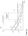
- FIG. 10illustrates power transfer improvements according to some embodiments.
- Chart 1000 of FIG. 10shows circuit voltage in comparison with the rectified BEMF voltage in the spindle motor.
- Curve 1010corresponds to power transfer utilizing synchronous rectification driving the logic load. Peak voltage generated by synchronous rectification is indicated as 1060 , and time available to power the load is indicated as region 1002 . As can be seen, a few milliseconds are available to program data into non-volatile memory before Vpwr drops below the minimum required Vpwr voltage 1050 .
- Curve 1020corresponds to power transfer utilizing boost brake circuit driving the logic load.
- the higher peak voltage generated by the boost brake circuitwhich is indicated as voltage difference 1062 , allows for a longer usable spin down time.
- consistent impedance of the boost brake circuitmakes the performance more predictable. Thus, longer time is available to power the load when compared to synchronous rectification, as is indicated by region 1004 .
- Dotted piecewise curve 1030corresponds to power transfer utilizing synchronous rectification with demand regulation. Curve 1030 overlaps with parts of the curve 1010 . Because losses in the windings of the spindle motor are minimized, longer time is available to power the load and to program non-volatile memory, as is indicated by regions 1004 and 1006 .
- Dotted piecewise curve 1050corresponds to power transfer utilizing boost braking with demand regulation. Curve 1050 overlaps with parts of the curve 1020 . Because losses in the windings of the spindle motor are minimized, longer time is available to power the load and to program non-volatile memory, as is indicated by region 1006 . Hence, demand regulation extends the total time during which non-volatile memory can be programmed and lowers the rate of power usage. This results in a more efficient power transfer, which in turn substantially increases the total amount of volatile memory cache that can be used to store data during normal operation since the more data in the cache can be saved to non-volatile memory in the event of a power interruption.
- logic load circuit support using demand regulation with boost brakingimproves energy transfer and extends spin down time.
- demand regulation with boost brakingprovides for more optimal power transfer than demand regulation with synchronous rectification.
- non-volatile memorymay comprise a wide variety of technologies, such as flash integrated circuits, Chalcogenide RAM (C-RAM), Phase Change Memory (PC-RAM or PRAM), Programmable Metallization Cell RAM (PMC-RAM or PMCm), Ovonic Unified Memory (OUM), Resistance RAM (RRAM), NAND memory, Single-Level Cell (SLC) memory, Multi-Level Cell (MLC) memory, NOR memory, EEPROM, Ferroelectric Memory (FeRAM), or other discrete NVM (non-volatile memory) chips.
- the solid-state storage devicese.g., dies
- non-volatile memorymay include a disk drive, as is described in U.S. Pat. No. 7,800,856, the disclosure of which is hereby incorporated by reference in its entirety.
- the various components illustrated in the figuresmay be implemented as software and/or firmware on a processor, ASIC/FPGA, or dedicated hardware. Also, the features and attributes of the specific embodiments disclosed above may be combined in different ways to form additional embodiments, all of which fall within the scope of the present disclosure.
Landscapes
- Engineering & Computer Science (AREA)
- Theoretical Computer Science (AREA)
- Quality & Reliability (AREA)
- Physics & Mathematics (AREA)
- General Engineering & Computer Science (AREA)
- General Physics & Mathematics (AREA)
- Power Sources (AREA)
- Dc-Dc Converters (AREA)
Abstract
Description
Claims (22)
Priority Applications (3)
| Application Number | Priority Date | Filing Date | Title |
|---|---|---|---|
| US13/239,176US8630054B2 (en) | 2011-09-21 | 2011-09-21 | Systems and methods for data throttling during disk drive power down |
| CN2012103571886ACN103021435A (en) | 2011-09-21 | 2012-09-21 | Systems and methods for data throttling during disk drive power down |
| US14/074,592US9001449B1 (en) | 2011-09-21 | 2013-11-07 | Systems and methods for data throttling during disk drive power down |
Applications Claiming Priority (1)
| Application Number | Priority Date | Filing Date | Title |
|---|---|---|---|
| US13/239,176US8630054B2 (en) | 2011-09-21 | 2011-09-21 | Systems and methods for data throttling during disk drive power down |
Related Child Applications (1)
| Application Number | Title | Priority Date | Filing Date |
|---|---|---|---|
| US14/074,592ContinuationUS9001449B1 (en) | 2011-09-21 | 2013-11-07 | Systems and methods for data throttling during disk drive power down |
Publications (2)
| Publication Number | Publication Date |
|---|---|
| US20130070363A1 US20130070363A1 (en) | 2013-03-21 |
| US8630054B2true US8630054B2 (en) | 2014-01-14 |
Family
ID=47880446
Family Applications (2)
| Application Number | Title | Priority Date | Filing Date |
|---|---|---|---|
| US13/239,176Expired - Fee RelatedUS8630054B2 (en) | 2011-09-21 | 2011-09-21 | Systems and methods for data throttling during disk drive power down |
| US14/074,592ActiveUS9001449B1 (en) | 2011-09-21 | 2013-11-07 | Systems and methods for data throttling during disk drive power down |
Family Applications After (1)
| Application Number | Title | Priority Date | Filing Date |
|---|---|---|---|
| US14/074,592ActiveUS9001449B1 (en) | 2011-09-21 | 2013-11-07 | Systems and methods for data throttling during disk drive power down |
Country Status (2)
| Country | Link |
|---|---|
| US (2) | US8630054B2 (en) |
| CN (1) | CN103021435A (en) |
Cited By (106)
| Publication number | Priority date | Publication date | Assignee | Title |
|---|---|---|---|---|
| US20130148240A1 (en)* | 2011-12-09 | 2013-06-13 | Western Digital Technologies, Inc. | Disk drive charging capacitor using motor supply voltage during power failure |
| US8824081B1 (en) | 2012-03-13 | 2014-09-02 | Western Digital Technologies, Inc. | Disk drive employing radially coherent reference pattern for servo burst demodulation and fly height measurement |
| US8830617B1 (en) | 2013-05-30 | 2014-09-09 | Western Digital Technologies, Inc. | Disk drive adjusting state estimator to compensate for unreliable servo data |
| US20140300993A1 (en)* | 2013-04-05 | 2014-10-09 | Rohm Co., Ltd. | Motor drive device, magnetic disk storage device, and electronic appliance |
| US8879191B1 (en) | 2012-11-14 | 2014-11-04 | Western Digital Technologies, Inc. | Disk drive modifying rotational position optimization algorithm to achieve target performance for limited stroke |
| US8891194B1 (en) | 2013-05-14 | 2014-11-18 | Western Digital Technologies, Inc. | Disk drive iteratively adapting correction value that compensates for non-linearity of head |
| US8891191B1 (en) | 2014-05-06 | 2014-11-18 | Western Digital Technologies, Inc. | Data storage device initializing read signal gain to detect servo seed pattern |
| US8896957B1 (en) | 2013-05-10 | 2014-11-25 | Western Digital Technologies, Inc. | Disk drive performing spiral scan of disk surface to detect residual data |
| US8902538B1 (en) | 2013-03-29 | 2014-12-02 | Western Digital Technologies, Inc. | Disk drive detecting crack in microactuator |
| US8902539B1 (en) | 2014-05-13 | 2014-12-02 | Western Digital Technologies, Inc. | Data storage device reducing seek power consumption |
| US8913342B1 (en) | 2014-03-21 | 2014-12-16 | Western Digital Technologies, Inc. | Data storage device adjusting range of microactuator digital-to-analog converter based on operating temperature |
| US8917474B1 (en) | 2011-08-08 | 2014-12-23 | Western Digital Technologies, Inc. | Disk drive calibrating a velocity profile prior to writing a spiral track |
| US8917475B1 (en) | 2013-12-20 | 2014-12-23 | Western Digital Technologies, Inc. | Disk drive generating a disk locked clock using radial dependent timing feed-forward compensation |
| US8922938B1 (en) | 2012-11-02 | 2014-12-30 | Western Digital Technologies, Inc. | Disk drive filtering disturbance signal and error signal for adaptive feed-forward compensation |
| US8922937B1 (en) | 2012-04-19 | 2014-12-30 | Western Digital Technologies, Inc. | Disk drive evaluating multiple vibration sensor outputs to enable write-protection |
| US8922931B1 (en) | 2013-05-13 | 2014-12-30 | Western Digital Technologies, Inc. | Disk drive releasing variable amount of buffered write data based on sliding window of predicted servo quality |
| US8922940B1 (en) | 2014-05-27 | 2014-12-30 | Western Digital Technologies, Inc. | Data storage device reducing spindle motor voltage boost during power failure |
| US8929021B1 (en) | 2012-03-27 | 2015-01-06 | Western Digital Technologies, Inc. | Disk drive servo writing from spiral tracks using radial dependent timing feed-forward compensation |
| US8929022B1 (en) | 2012-12-19 | 2015-01-06 | Western Digital Technologies, Inc. | Disk drive detecting microactuator degradation by evaluating frequency component of servo signal |
| US8934186B1 (en) | 2014-03-26 | 2015-01-13 | Western Digital Technologies, Inc. | Data storage device estimating servo zone to reduce size of track address |
| US8937784B1 (en) | 2012-08-01 | 2015-01-20 | Western Digital Technologies, Inc. | Disk drive employing feed-forward compensation and phase shift compensation during seek settling |
| US8941939B1 (en) | 2013-10-24 | 2015-01-27 | Western Digital Technologies, Inc. | Disk drive using VCM BEMF feed-forward compensation to write servo data to a disk |
| US8941945B1 (en) | 2014-06-06 | 2015-01-27 | Western Digital Technologies, Inc. | Data storage device servoing heads based on virtual servo tracks |
| US8947819B1 (en) | 2012-08-28 | 2015-02-03 | Western Digital Technologies, Inc. | Disk drive implementing hysteresis for primary shock detector based on a more sensitive secondary shock detector |
| US8953271B1 (en) | 2013-05-13 | 2015-02-10 | Western Digital Technologies, Inc. | Disk drive compensating for repeatable run out selectively per zone |
| US8953278B1 (en) | 2011-11-16 | 2015-02-10 | Western Digital Technologies, Inc. | Disk drive selecting disturbance signal for feed-forward compensation |
| US8958169B1 (en) | 2014-06-11 | 2015-02-17 | Western Digital Technologies, Inc. | Data storage device re-qualifying state estimator while decelerating head |
| US8970979B1 (en) | 2013-12-18 | 2015-03-03 | Western Digital Technologies, Inc. | Disk drive determining frequency response of actuator near servo sample frequency |
| US8982490B1 (en) | 2014-04-24 | 2015-03-17 | Western Digital Technologies, Inc. | Data storage device reading first spiral track while simultaneously writing second spiral track |
| US8982501B1 (en) | 2014-09-22 | 2015-03-17 | Western Digital Technologies, Inc. | Data storage device compensating for repeatable disturbance when commutating a spindle motor |
| US8995075B1 (en) | 2012-06-21 | 2015-03-31 | Western Digital Technologies, Inc. | Disk drive adjusting estimated servo state to compensate for transient when crossing a servo zone boundary |
| US8995082B1 (en) | 2011-06-03 | 2015-03-31 | Western Digital Technologies, Inc. | Reducing acoustic noise in a disk drive when exiting idle mode |
| US9001454B1 (en) | 2013-04-12 | 2015-04-07 | Western Digital Technologies, Inc. | Disk drive adjusting phase of adaptive feed-forward controller when reconfiguring servo loop |
| US9001449B1 (en) | 2011-09-21 | 2015-04-07 | Western Digital Technologies, Inc. | Systems and methods for data throttling during disk drive power down |
| US9007714B1 (en) | 2014-07-18 | 2015-04-14 | Western Digital Technologies Inc. | Data storage device comprising slew rate anti-windup compensation for microactuator |
| US9013824B1 (en) | 2014-06-04 | 2015-04-21 | Western Digital Technologies, Inc. | Data storage device comprising dual read sensors and dual servo channels to improve servo demodulation |
| US9013825B1 (en) | 2014-03-24 | 2015-04-21 | Western Digital Technologies, Inc. | Electronic system with vibration management mechanism and method of operation thereof |
| US9026728B1 (en) | 2013-06-06 | 2015-05-05 | Western Digital Technologies, Inc. | Disk drive applying feed-forward compensation when writing consecutive data tracks |
| US9025269B1 (en) | 2014-01-02 | 2015-05-05 | Western Digital Technologies, Inc. | Disk drive compensating for cycle slip of disk locked clock when reading mini-wedge |
| US9047901B1 (en) | 2013-05-28 | 2015-06-02 | Western Digital Technologies, Inc. | Disk drive measuring spiral track error by measuring a slope of a spiral track across a disk radius |
| US9047919B1 (en) | 2013-03-12 | 2015-06-02 | Western Digitial Technologies, Inc. | Disk drive initializing servo read channel by reading data preceding servo preamble during access operation |
| US9047932B1 (en)* | 2014-03-21 | 2015-06-02 | Western Digital Technologies, Inc. | Data storage device adjusting a power loss threshold based on samples of supply voltage |
| US9053726B1 (en) | 2014-01-29 | 2015-06-09 | Western Digital Technologies, Inc. | Data storage device on-line adapting disturbance observer filter |
| US9053727B1 (en) | 2014-06-02 | 2015-06-09 | Western Digital Technologies, Inc. | Disk drive opening spiral crossing window based on DC and AC spiral track error |
| US9053712B1 (en) | 2014-05-07 | 2015-06-09 | Western Digital Technologies, Inc. | Data storage device reading servo sector while writing data sector |
| US9058827B1 (en) | 2013-06-25 | 2015-06-16 | Western Digitial Technologies, Inc. | Disk drive optimizing filters based on sensor signal and disturbance signal for adaptive feed-forward compensation |
| US9058834B1 (en) | 2013-11-08 | 2015-06-16 | Western Digital Technologies, Inc. | Power architecture for low power modes in storage devices |
| US9058826B1 (en) | 2014-02-13 | 2015-06-16 | Western Digital Technologies, Inc. | Data storage device detecting free fall condition from disk speed variations |
| US9064537B1 (en) | 2013-09-13 | 2015-06-23 | Western Digital Technologies, Inc. | Disk drive measuring radial offset between heads by detecting a difference between ramp contact |
| US9076472B1 (en) | 2014-08-21 | 2015-07-07 | Western Digital (Fremont), Llc | Apparatus enabling writing servo data when disk reaches target rotation speed |
| US9076490B1 (en) | 2012-12-12 | 2015-07-07 | Western Digital Technologies, Inc. | Disk drive writing radial offset spiral servo tracks by reading spiral seed tracks |
| US9076473B1 (en) | 2014-08-12 | 2015-07-07 | Western Digital Technologies, Inc. | Data storage device detecting fly height instability of head during load operation based on microactuator response |
| US9076471B1 (en) | 2013-07-31 | 2015-07-07 | Western Digital Technologies, Inc. | Fall detection scheme using FFS |
| US9099147B1 (en) | 2014-09-22 | 2015-08-04 | Western Digital Technologies, Inc. | Data storage device commutating a spindle motor using closed-loop rotation phase alignment |
| US9111575B1 (en) | 2014-10-23 | 2015-08-18 | Western Digital Technologies, Inc. | Data storage device employing adaptive feed-forward control in timing loop to compensate for vibration |
| US9129630B1 (en) | 2014-12-16 | 2015-09-08 | Western Digital Technologies, Inc. | Data storage device employing full servo sectors on first disk surface and mini servo sectors on second disk surface |
| US9142249B1 (en) | 2013-12-06 | 2015-09-22 | Western Digital Technologies, Inc. | Disk drive using timing loop control signal for vibration compensation in servo loop |
| US9142225B1 (en) | 2014-03-21 | 2015-09-22 | Western Digital Technologies, Inc. | Electronic system with actuator control mechanism and method of operation thereof |
| US9141177B1 (en) | 2014-03-21 | 2015-09-22 | Western Digital Technologies, Inc. | Data storage device employing glitch compensation for power loss detection |
| US9142235B1 (en) | 2009-10-27 | 2015-09-22 | Western Digital Technologies, Inc. | Disk drive characterizing microactuator by injecting sinusoidal disturbance and evaluating feed-forward compensation values |
| US9147418B1 (en) | 2013-06-20 | 2015-09-29 | Western Digital Technologies, Inc. | Disk drive compensating for microactuator gain variations |
| US9147428B1 (en) | 2013-04-24 | 2015-09-29 | Western Digital Technologies, Inc. | Disk drive with improved spin-up control |
| US9153283B1 (en) | 2014-09-30 | 2015-10-06 | Western Digital Technologies, Inc. | Data storage device compensating for hysteretic response of microactuator |
| US9165583B1 (en) | 2014-10-29 | 2015-10-20 | Western Digital Technologies, Inc. | Data storage device adjusting seek profile based on seek length when ending track is near ramp |
| US9171567B1 (en) | 2014-05-27 | 2015-10-27 | Western Digital Technologies, Inc. | Data storage device employing sliding mode control of spindle motor |
| US9171568B1 (en) | 2014-06-25 | 2015-10-27 | Western Digital Technologies, Inc. | Data storage device periodically re-initializing spindle motor commutation sequence based on timing data |
| US9208810B1 (en) | 2014-04-24 | 2015-12-08 | Western Digital Technologies, Inc. | Data storage device attenuating interference from first spiral track when reading second spiral track |
| US9208815B1 (en) | 2014-10-09 | 2015-12-08 | Western Digital Technologies, Inc. | Data storage device dynamically reducing coast velocity during seek to reduce power consumption |
| US9208808B1 (en) | 2014-04-22 | 2015-12-08 | Western Digital Technologies, Inc. | Electronic system with unload management mechanism and method of operation thereof |
| US9214175B1 (en) | 2015-03-16 | 2015-12-15 | Western Digital Technologies, Inc. | Data storage device configuring a gain of a servo control system for actuating a head over a disk |
| US9230593B1 (en) | 2014-12-23 | 2016-01-05 | Western Digital Technologies, Inc. | Data storage device optimizing spindle motor power when transitioning into a power failure mode |
| US9230592B1 (en) | 2014-12-23 | 2016-01-05 | Western Digital Technologies, Inc. | Electronic system with a method of motor spindle bandwidth estimation and calibration thereof |
| US9245560B1 (en) | 2015-03-09 | 2016-01-26 | Western Digital Technologies, Inc. | Data storage device measuring reader/writer offset by reading spiral track and concentric servo sectors |
| US9245577B1 (en) | 2015-03-26 | 2016-01-26 | Western Digital Technologies, Inc. | Data storage device comprising spindle motor current sensing with supply voltage noise attenuation |
| US9245540B1 (en) | 2014-10-29 | 2016-01-26 | Western Digital Technologies, Inc. | Voice coil motor temperature sensing circuit to reduce catastrophic failure due to voice coil motor coil shorting to ground |
| US9251823B1 (en) | 2014-12-10 | 2016-02-02 | Western Digital Technologies, Inc. | Data storage device delaying seek operation to avoid thermal asperities |
| US9269386B1 (en) | 2014-01-29 | 2016-02-23 | Western Digital Technologies, Inc. | Data storage device on-line adapting disturbance observer filter |
| US9286925B1 (en) | 2015-03-26 | 2016-03-15 | Western Digital Technologies, Inc. | Data storage device writing multiple burst correction values at the same radial location |
| US9286927B1 (en) | 2014-12-16 | 2016-03-15 | Western Digital Technologies, Inc. | Data storage device demodulating servo burst by computing slope of intermediate integration points |
| US9343102B1 (en) | 2015-03-25 | 2016-05-17 | Western Digital Technologies, Inc. | Data storage device employing a phase offset to generate power from a spindle motor during a power failure |
| US9343094B1 (en) | 2015-03-26 | 2016-05-17 | Western Digital Technologies, Inc. | Data storage device filtering burst correction values before downsampling the burst correction values |
| US9349401B1 (en) | 2014-07-24 | 2016-05-24 | Western Digital Technologies, Inc. | Electronic system with media scan mechanism and method of operation thereof |
| US9350278B1 (en) | 2014-06-13 | 2016-05-24 | Western Digital Technologies, Inc. | Circuit technique to integrate voice coil motor support elements |
| US9355676B1 (en) | 2015-03-25 | 2016-05-31 | Western Digital Technologies, Inc. | Data storage device controlling amplitude and phase of driving voltage to generate power from a spindle motor |
| US9355667B1 (en) | 2014-11-11 | 2016-05-31 | Western Digital Technologies, Inc. | Data storage device saving absolute position at each servo wedge for previous write operations |
| US9361939B1 (en) | 2014-03-10 | 2016-06-07 | Western Digital Technologies, Inc. | Data storage device characterizing geometry of magnetic transitions |
| US9396751B1 (en) | 2015-06-26 | 2016-07-19 | Western Digital Technologies, Inc. | Data storage device compensating for fabrication tolerances when measuring spindle motor current |
| US9407015B1 (en) | 2014-12-29 | 2016-08-02 | Western Digital Technologies, Inc. | Automatic power disconnect device |
| US9418689B2 (en) | 2014-10-09 | 2016-08-16 | Western Digital Technologies, Inc. | Data storage device generating an operating seek time profile as a function of a base seek time profile |
| US9424868B1 (en) | 2015-05-12 | 2016-08-23 | Western Digital Technologies, Inc. | Data storage device employing spindle motor driving profile during seek to improve power performance |
| US9424871B1 (en) | 2012-09-13 | 2016-08-23 | Western Digital Technologies, Inc. | Disk drive correcting an error in a detected gray code |
| US9437237B1 (en) | 2015-02-20 | 2016-09-06 | Western Digital Technologies, Inc. | Method to detect power loss through data storage device spindle speed |
| US9437231B1 (en) | 2015-09-25 | 2016-09-06 | Western Digital Technologies, Inc. | Data storage device concurrently controlling and sensing a secondary actuator for actuating a head over a disk |
| US9454212B1 (en) | 2014-12-08 | 2016-09-27 | Western Digital Technologies, Inc. | Wakeup detector |
| US9471072B1 (en) | 2013-11-14 | 2016-10-18 | Western Digital Technologies, Inc | Self-adaptive voltage scaling |
| US9484733B1 (en) | 2013-09-11 | 2016-11-01 | Western Digital Technologies, Inc. | Power control module for data storage device |
| US9542966B1 (en) | 2015-07-09 | 2017-01-10 | Western Digital Technologies, Inc. | Data storage devices and methods with frequency-shaped sliding mode control |
| US9564162B1 (en) | 2015-12-28 | 2017-02-07 | Western Digital Technologies, Inc. | Data storage device measuring resonant frequency of a shock sensor by applying differential excitation and measuring oscillation |
| US9581978B1 (en) | 2014-12-17 | 2017-02-28 | Western Digital Technologies, Inc. | Electronic system with servo management mechanism and method of operation thereof |
| US9620160B1 (en) | 2015-12-28 | 2017-04-11 | Western Digital Technologies, Inc. | Data storage device measuring resonant frequency of a shock sensor by inserting the shock sensor into an oscillator circuit |
| US9823294B1 (en) | 2013-10-29 | 2017-11-21 | Western Digital Technologies, Inc. | Negative voltage testing methodology and tester |
| US9886285B2 (en) | 2015-03-31 | 2018-02-06 | Western Digital Technologies, Inc. | Communication interface initialization |
| US9899834B1 (en) | 2015-11-18 | 2018-02-20 | Western Digital Technologies, Inc. | Power control module using protection circuit for regulating backup voltage to power load during power fault |
| US9959204B1 (en) | 2015-03-09 | 2018-05-01 | Western Digital Technologies, Inc. | Tracking sequential ranges of non-ordered data |
| US10242698B1 (en) | 2018-04-19 | 2019-03-26 | Western Digital Technologies, Inc. | Data storage device regulating BEMF power voltage during power failure |
| US11016901B2 (en) | 2018-12-10 | 2021-05-25 | International Business Machines Corporation | Storage system de-throttling to facilitate emergency cache destage |
Families Citing this family (18)
| Publication number | Priority date | Publication date | Assignee | Title |
|---|---|---|---|---|
| US8947813B2 (en)* | 2012-12-07 | 2015-02-03 | HGST Netherlands B.V. | Emergency power off (EPO) island for saving critical data to non-volatile memory |
| US9619330B2 (en)* | 2013-10-08 | 2017-04-11 | Seagate Technology Llc | Protecting volatile data of a storage device in response to a state reset |
| US9870281B1 (en)* | 2015-03-20 | 2018-01-16 | Western Digital Technologies, Inc. | Power loss mitigation for data storage device |
| US9658634B2 (en)* | 2015-03-30 | 2017-05-23 | Apple Inc. | Under voltage detection and performance throttling |
| US10083736B1 (en) | 2016-06-23 | 2018-09-25 | Apple Inc. | Adaptive calibration scheduling for a memory subsystem based on calibrations of delay applied to data strobe and calibration of reference voltage |
| US10418115B2 (en)* | 2017-07-07 | 2019-09-17 | Micron Technology, Inc. | Managed NAND performance throttling |
| JP6953211B2 (en)* | 2017-07-18 | 2021-10-27 | キヤノン株式会社 | Information processing device and control method of information processing device |
| US10242706B1 (en)* | 2018-04-29 | 2019-03-26 | Western Digital Technologies, Inc. | Data storage device detecting spindle motor position at increased resolution using mutual inductive sense |
| KR20200036627A (en)* | 2018-09-28 | 2020-04-07 | 에스케이하이닉스 주식회사 | Memory system and operating method thereof |
| US11226752B2 (en) | 2019-03-05 | 2022-01-18 | Apple Inc. | Filtering memory calibration |
| JP2020149753A (en)* | 2019-03-15 | 2020-09-17 | 株式会社東芝 | Control device and magnetic disk device |
| US10996862B2 (en)* | 2019-06-17 | 2021-05-04 | Western Digital Technologies, Inc. | Adaptive read trim for second read data retention |
| US11520521B2 (en)* | 2019-06-20 | 2022-12-06 | Western Digital Technologies, Inc. | Storage controller having data augmentation components for use with non-volatile memory die |
| US11126248B2 (en)* | 2019-06-25 | 2021-09-21 | Western Digital Technologies, Inc. | Data storage device detecting supply current limit |
| JP2021034088A (en)* | 2019-08-28 | 2021-03-01 | 株式会社東芝 | Magnetic disk device and data protection method for the magnetic disk device |
| CN113702891B (en)* | 2020-05-22 | 2025-05-30 | 深圳市星龙科技股份有限公司 | Charging pile error detection device and method |
| US20230229222A1 (en)* | 2020-07-13 | 2023-07-20 | Intel Corporation | Voltage protection |
| US11763844B1 (en)* | 2022-04-08 | 2023-09-19 | Western Digital Technologies, Inc. | Data storage device having dual actuators and method for emergency power off retract (EPOR) of dual actuators |
Citations (22)
| Publication number | Priority date | Publication date | Assignee | Title |
|---|---|---|---|---|
| US6295577B1 (en) | 1998-02-24 | 2001-09-25 | Seagate Technology Llc | Disc storage system having a non-volatile cache to store write data in the event of a power failure |
| US6516426B1 (en) | 1999-01-11 | 2003-02-04 | Seagate Technology Llc | Disc storage system having non-volatile write cache |
| US6549359B1 (en) | 2000-04-19 | 2003-04-15 | Western Digital Technologies, Inc. | Disk drive comprising spin down circuitry having a current limit circuit for enhancing power and braking control |
| US6566832B2 (en)* | 1999-06-02 | 2003-05-20 | Maxtor Corporation | Method and apparatus for parking a read/write head during power interruptions by dynamic sequencing |
| US6574062B1 (en) | 2000-04-19 | 2003-06-03 | Western Digital Technologies, Inc. | Disk drive comprising a demand limit circuit for enhancing power management during spin down |
| US6725397B1 (en) | 2000-11-14 | 2004-04-20 | International Business Machines Corporation | Method and system for preserving data resident in volatile cache memory in the event of a power loss |
| US20040158771A1 (en) | 2003-02-10 | 2004-08-12 | Garnett Paul J. | Adaptive throttling |
| US20050125600A1 (en) | 2003-12-04 | 2005-06-09 | Ehrlich Richard M. | Method for storing HDD critical data in flash |
| US6957355B2 (en) | 2002-09-18 | 2005-10-18 | Sun Microsystems, Inc. | Method and system for dynamically adjusting storage system write cache based on the backup battery level |
| US6970319B1 (en) | 2003-05-27 | 2005-11-29 | Western Digital Technologies, Inc. | Disk drive comprising a pulse width modulated demand limit circuit for enhancing power management during spin-down |
| US7062675B1 (en) | 2002-06-25 | 2006-06-13 | Emc Corporation | Data storage cache system shutdown scheme |
| US7068460B2 (en) | 2004-07-22 | 2006-06-27 | Agere Systems Inc. | Low cost emergency disk drive head retract architecture |
| US7082373B2 (en) | 2003-01-31 | 2006-07-25 | Microsoft Corporation | Dynamic power control apparatus, systems and methods |
| US7161757B1 (en) | 1999-02-25 | 2007-01-09 | Stmicroelectronics Asia Pacific (Pte) Ltd. | Method and apparatus for controlling a disk drive under a power loss condition |
| US20070219747A1 (en) | 2006-03-07 | 2007-09-20 | Hughes James E | HDD throttle polling based on blade temperature |
| US7309967B2 (en) | 2004-03-31 | 2007-12-18 | Hitachi Global Storage Technologies Netherlands B.V. | Motor drive circuitry with regenerative braking for disk drive |
| US7430089B2 (en) | 2005-03-14 | 2008-09-30 | Fujitsu Limited | Data storage device and write processing method for data storage device |
| US7633702B1 (en) | 2000-03-31 | 2009-12-15 | Seagate Technology Llc | Method and apparatus for powering voice coil motor retract circuit while braking spindle |
| US7661002B2 (en) | 2005-08-04 | 2010-02-09 | Dot Hill Systems Corporation | Storage controller super capacitor dynamic voltage throttling |
| US7800856B1 (en) | 2009-03-24 | 2010-09-21 | Western Digital Technologies, Inc. | Disk drive flushing write cache to a nearest set of reserved tracks during a power failure |
| US7907634B2 (en) | 2004-01-29 | 2011-03-15 | Hildebrand John G | Method and system of transporting multimedia signals |
| US7974038B2 (en) | 2007-12-10 | 2011-07-05 | Western Digital Technologies, Inc. | Servo writer with retract capacitor for generating a VCM driving current during a power failure |
Family Cites Families (2)
| Publication number | Priority date | Publication date | Assignee | Title |
|---|---|---|---|---|
| JP4421485B2 (en)* | 2005-01-25 | 2010-02-24 | 株式会社東芝 | Head retraction method at power-off and disk storage device to which the method is applied |
| US8630054B2 (en) | 2011-09-21 | 2014-01-14 | Western Digital Technologies, Inc. | Systems and methods for data throttling during disk drive power down |
- 2011
- 2011-09-21USUS13/239,176patent/US8630054B2/ennot_activeExpired - Fee Related
- 2012
- 2012-09-21CNCN2012103571886Apatent/CN103021435A/enactivePending
- 2013
- 2013-11-07USUS14/074,592patent/US9001449B1/enactiveActive
Patent Citations (25)
| Publication number | Priority date | Publication date | Assignee | Title |
|---|---|---|---|---|
| US6295577B1 (en) | 1998-02-24 | 2001-09-25 | Seagate Technology Llc | Disc storage system having a non-volatile cache to store write data in the event of a power failure |
| US6516426B1 (en) | 1999-01-11 | 2003-02-04 | Seagate Technology Llc | Disc storage system having non-volatile write cache |
| US7161757B1 (en) | 1999-02-25 | 2007-01-09 | Stmicroelectronics Asia Pacific (Pte) Ltd. | Method and apparatus for controlling a disk drive under a power loss condition |
| US6566832B2 (en)* | 1999-06-02 | 2003-05-20 | Maxtor Corporation | Method and apparatus for parking a read/write head during power interruptions by dynamic sequencing |
| US7633702B1 (en) | 2000-03-31 | 2009-12-15 | Seagate Technology Llc | Method and apparatus for powering voice coil motor retract circuit while braking spindle |
| US6549359B1 (en) | 2000-04-19 | 2003-04-15 | Western Digital Technologies, Inc. | Disk drive comprising spin down circuitry having a current limit circuit for enhancing power and braking control |
| US6549361B1 (en) | 2000-04-19 | 2003-04-15 | Western Digital Technologies, Inc. | Disk drive comprising spin down circuitry having a power clamp circuit for enhancing power and braking control |
| US6574062B1 (en) | 2000-04-19 | 2003-06-03 | Western Digital Technologies, Inc. | Disk drive comprising a demand limit circuit for enhancing power management during spin down |
| US6577465B1 (en) | 2000-04-19 | 2003-06-10 | Western Digital Technologies, Inc. | Disk drive comprising spin down circuitry having a programmable signal generator for enhancing power and braking control |
| US6725397B1 (en) | 2000-11-14 | 2004-04-20 | International Business Machines Corporation | Method and system for preserving data resident in volatile cache memory in the event of a power loss |
| US7062675B1 (en) | 2002-06-25 | 2006-06-13 | Emc Corporation | Data storage cache system shutdown scheme |
| US6957355B2 (en) | 2002-09-18 | 2005-10-18 | Sun Microsystems, Inc. | Method and system for dynamically adjusting storage system write cache based on the backup battery level |
| US7082373B2 (en) | 2003-01-31 | 2006-07-25 | Microsoft Corporation | Dynamic power control apparatus, systems and methods |
| US20040158771A1 (en) | 2003-02-10 | 2004-08-12 | Garnett Paul J. | Adaptive throttling |
| US7124321B2 (en) | 2003-02-10 | 2006-10-17 | Sun Microsystems, Inc. | Adaptive throttling |
| US6970319B1 (en) | 2003-05-27 | 2005-11-29 | Western Digital Technologies, Inc. | Disk drive comprising a pulse width modulated demand limit circuit for enhancing power management during spin-down |
| US20050125600A1 (en) | 2003-12-04 | 2005-06-09 | Ehrlich Richard M. | Method for storing HDD critical data in flash |
| US7907634B2 (en) | 2004-01-29 | 2011-03-15 | Hildebrand John G | Method and system of transporting multimedia signals |
| US7309967B2 (en) | 2004-03-31 | 2007-12-18 | Hitachi Global Storage Technologies Netherlands B.V. | Motor drive circuitry with regenerative braking for disk drive |
| US7068460B2 (en) | 2004-07-22 | 2006-06-27 | Agere Systems Inc. | Low cost emergency disk drive head retract architecture |
| US7430089B2 (en) | 2005-03-14 | 2008-09-30 | Fujitsu Limited | Data storage device and write processing method for data storage device |
| US7661002B2 (en) | 2005-08-04 | 2010-02-09 | Dot Hill Systems Corporation | Storage controller super capacitor dynamic voltage throttling |
| US20070219747A1 (en) | 2006-03-07 | 2007-09-20 | Hughes James E | HDD throttle polling based on blade temperature |
| US7974038B2 (en) | 2007-12-10 | 2011-07-05 | Western Digital Technologies, Inc. | Servo writer with retract capacitor for generating a VCM driving current during a power failure |
| US7800856B1 (en) | 2009-03-24 | 2010-09-21 | Western Digital Technologies, Inc. | Disk drive flushing write cache to a nearest set of reserved tracks during a power failure |
Cited By (114)
| Publication number | Priority date | Publication date | Assignee | Title |
|---|---|---|---|---|
| US9142235B1 (en) | 2009-10-27 | 2015-09-22 | Western Digital Technologies, Inc. | Disk drive characterizing microactuator by injecting sinusoidal disturbance and evaluating feed-forward compensation values |
| US8995082B1 (en) | 2011-06-03 | 2015-03-31 | Western Digital Technologies, Inc. | Reducing acoustic noise in a disk drive when exiting idle mode |
| US8917474B1 (en) | 2011-08-08 | 2014-12-23 | Western Digital Technologies, Inc. | Disk drive calibrating a velocity profile prior to writing a spiral track |
| US9001449B1 (en) | 2011-09-21 | 2015-04-07 | Western Digital Technologies, Inc. | Systems and methods for data throttling during disk drive power down |
| US8953278B1 (en) | 2011-11-16 | 2015-02-10 | Western Digital Technologies, Inc. | Disk drive selecting disturbance signal for feed-forward compensation |
| US9093105B2 (en)* | 2011-12-09 | 2015-07-28 | Western Digital Technologies, Inc. | Disk drive charging capacitor using motor supply voltage during power failure |
| US20130148240A1 (en)* | 2011-12-09 | 2013-06-13 | Western Digital Technologies, Inc. | Disk drive charging capacitor using motor supply voltage during power failure |
| US9390749B2 (en)* | 2011-12-09 | 2016-07-12 | Western Digital Technologies, Inc. | Power failure management in disk drives |
| US20150310886A1 (en)* | 2011-12-09 | 2015-10-29 | Western Digital Technologies, Inc. | Power failure management in disk drives |
| US8824081B1 (en) | 2012-03-13 | 2014-09-02 | Western Digital Technologies, Inc. | Disk drive employing radially coherent reference pattern for servo burst demodulation and fly height measurement |
| US8934191B1 (en) | 2012-03-27 | 2015-01-13 | Western Digital Technologies, Inc. | Disk drive generating a disk locked clock using radial dependent timing feed-forward compensation |
| US8929021B1 (en) | 2012-03-27 | 2015-01-06 | Western Digital Technologies, Inc. | Disk drive servo writing from spiral tracks using radial dependent timing feed-forward compensation |
| US8922937B1 (en) | 2012-04-19 | 2014-12-30 | Western Digital Technologies, Inc. | Disk drive evaluating multiple vibration sensor outputs to enable write-protection |
| US8995075B1 (en) | 2012-06-21 | 2015-03-31 | Western Digital Technologies, Inc. | Disk drive adjusting estimated servo state to compensate for transient when crossing a servo zone boundary |
| US9454989B1 (en) | 2012-06-21 | 2016-09-27 | Western Digital Technologies, Inc. | Disk drive adjusting estimated servo state to compensate for transient when crossing a servo zone boundary |
| US8937784B1 (en) | 2012-08-01 | 2015-01-20 | Western Digital Technologies, Inc. | Disk drive employing feed-forward compensation and phase shift compensation during seek settling |
| US8947819B1 (en) | 2012-08-28 | 2015-02-03 | Western Digital Technologies, Inc. | Disk drive implementing hysteresis for primary shock detector based on a more sensitive secondary shock detector |
| US9424871B1 (en) | 2012-09-13 | 2016-08-23 | Western Digital Technologies, Inc. | Disk drive correcting an error in a detected gray code |
| US8922938B1 (en) | 2012-11-02 | 2014-12-30 | Western Digital Technologies, Inc. | Disk drive filtering disturbance signal and error signal for adaptive feed-forward compensation |
| US8879191B1 (en) | 2012-11-14 | 2014-11-04 | Western Digital Technologies, Inc. | Disk drive modifying rotational position optimization algorithm to achieve target performance for limited stroke |
| US9076490B1 (en) | 2012-12-12 | 2015-07-07 | Western Digital Technologies, Inc. | Disk drive writing radial offset spiral servo tracks by reading spiral seed tracks |
| US8929022B1 (en) | 2012-12-19 | 2015-01-06 | Western Digital Technologies, Inc. | Disk drive detecting microactuator degradation by evaluating frequency component of servo signal |
| US9047919B1 (en) | 2013-03-12 | 2015-06-02 | Western Digitial Technologies, Inc. | Disk drive initializing servo read channel by reading data preceding servo preamble during access operation |
| US8902538B1 (en) | 2013-03-29 | 2014-12-02 | Western Digital Technologies, Inc. | Disk drive detecting crack in microactuator |
| US20140300993A1 (en)* | 2013-04-05 | 2014-10-09 | Rohm Co., Ltd. | Motor drive device, magnetic disk storage device, and electronic appliance |
| US9093106B2 (en)* | 2013-04-05 | 2015-07-28 | Rohm Co., Ltd. | Motor drive device, magnetic disk storage device, and electronic appliance |
| US9001454B1 (en) | 2013-04-12 | 2015-04-07 | Western Digital Technologies, Inc. | Disk drive adjusting phase of adaptive feed-forward controller when reconfiguring servo loop |
| US9147428B1 (en) | 2013-04-24 | 2015-09-29 | Western Digital Technologies, Inc. | Disk drive with improved spin-up control |
| US8896957B1 (en) | 2013-05-10 | 2014-11-25 | Western Digital Technologies, Inc. | Disk drive performing spiral scan of disk surface to detect residual data |
| US8922931B1 (en) | 2013-05-13 | 2014-12-30 | Western Digital Technologies, Inc. | Disk drive releasing variable amount of buffered write data based on sliding window of predicted servo quality |
| US8953271B1 (en) | 2013-05-13 | 2015-02-10 | Western Digital Technologies, Inc. | Disk drive compensating for repeatable run out selectively per zone |
| US8891194B1 (en) | 2013-05-14 | 2014-11-18 | Western Digital Technologies, Inc. | Disk drive iteratively adapting correction value that compensates for non-linearity of head |
| US9047901B1 (en) | 2013-05-28 | 2015-06-02 | Western Digital Technologies, Inc. | Disk drive measuring spiral track error by measuring a slope of a spiral track across a disk radius |
| US8830617B1 (en) | 2013-05-30 | 2014-09-09 | Western Digital Technologies, Inc. | Disk drive adjusting state estimator to compensate for unreliable servo data |
| US9026728B1 (en) | 2013-06-06 | 2015-05-05 | Western Digital Technologies, Inc. | Disk drive applying feed-forward compensation when writing consecutive data tracks |
| US9147418B1 (en) | 2013-06-20 | 2015-09-29 | Western Digital Technologies, Inc. | Disk drive compensating for microactuator gain variations |
| US9058827B1 (en) | 2013-06-25 | 2015-06-16 | Western Digitial Technologies, Inc. | Disk drive optimizing filters based on sensor signal and disturbance signal for adaptive feed-forward compensation |
| US9076471B1 (en) | 2013-07-31 | 2015-07-07 | Western Digital Technologies, Inc. | Fall detection scheme using FFS |
| US9484733B1 (en) | 2013-09-11 | 2016-11-01 | Western Digital Technologies, Inc. | Power control module for data storage device |
| US9064537B1 (en) | 2013-09-13 | 2015-06-23 | Western Digital Technologies, Inc. | Disk drive measuring radial offset between heads by detecting a difference between ramp contact |
| US8941939B1 (en) | 2013-10-24 | 2015-01-27 | Western Digital Technologies, Inc. | Disk drive using VCM BEMF feed-forward compensation to write servo data to a disk |
| US9823294B1 (en) | 2013-10-29 | 2017-11-21 | Western Digital Technologies, Inc. | Negative voltage testing methodology and tester |
| US9058834B1 (en) | 2013-11-08 | 2015-06-16 | Western Digital Technologies, Inc. | Power architecture for low power modes in storage devices |
| US9471072B1 (en) | 2013-11-14 | 2016-10-18 | Western Digital Technologies, Inc | Self-adaptive voltage scaling |
| US9142249B1 (en) | 2013-12-06 | 2015-09-22 | Western Digital Technologies, Inc. | Disk drive using timing loop control signal for vibration compensation in servo loop |
| US8970979B1 (en) | 2013-12-18 | 2015-03-03 | Western Digital Technologies, Inc. | Disk drive determining frequency response of actuator near servo sample frequency |
| US8917475B1 (en) | 2013-12-20 | 2014-12-23 | Western Digital Technologies, Inc. | Disk drive generating a disk locked clock using radial dependent timing feed-forward compensation |
| US9025269B1 (en) | 2014-01-02 | 2015-05-05 | Western Digital Technologies, Inc. | Disk drive compensating for cycle slip of disk locked clock when reading mini-wedge |
| US9053726B1 (en) | 2014-01-29 | 2015-06-09 | Western Digital Technologies, Inc. | Data storage device on-line adapting disturbance observer filter |
| US9269386B1 (en) | 2014-01-29 | 2016-02-23 | Western Digital Technologies, Inc. | Data storage device on-line adapting disturbance observer filter |
| US9058826B1 (en) | 2014-02-13 | 2015-06-16 | Western Digital Technologies, Inc. | Data storage device detecting free fall condition from disk speed variations |
| US9361939B1 (en) | 2014-03-10 | 2016-06-07 | Western Digital Technologies, Inc. | Data storage device characterizing geometry of magnetic transitions |
| US8913342B1 (en) | 2014-03-21 | 2014-12-16 | Western Digital Technologies, Inc. | Data storage device adjusting range of microactuator digital-to-analog converter based on operating temperature |
| US9047932B1 (en)* | 2014-03-21 | 2015-06-02 | Western Digital Technologies, Inc. | Data storage device adjusting a power loss threshold based on samples of supply voltage |
| US9142225B1 (en) | 2014-03-21 | 2015-09-22 | Western Digital Technologies, Inc. | Electronic system with actuator control mechanism and method of operation thereof |
| US9141177B1 (en) | 2014-03-21 | 2015-09-22 | Western Digital Technologies, Inc. | Data storage device employing glitch compensation for power loss detection |
| US9013825B1 (en) | 2014-03-24 | 2015-04-21 | Western Digital Technologies, Inc. | Electronic system with vibration management mechanism and method of operation thereof |
| US8934186B1 (en) | 2014-03-26 | 2015-01-13 | Western Digital Technologies, Inc. | Data storage device estimating servo zone to reduce size of track address |
| US9208808B1 (en) | 2014-04-22 | 2015-12-08 | Western Digital Technologies, Inc. | Electronic system with unload management mechanism and method of operation thereof |
| US8982490B1 (en) | 2014-04-24 | 2015-03-17 | Western Digital Technologies, Inc. | Data storage device reading first spiral track while simultaneously writing second spiral track |
| US9208810B1 (en) | 2014-04-24 | 2015-12-08 | Western Digital Technologies, Inc. | Data storage device attenuating interference from first spiral track when reading second spiral track |
| US8891191B1 (en) | 2014-05-06 | 2014-11-18 | Western Digital Technologies, Inc. | Data storage device initializing read signal gain to detect servo seed pattern |
| US9053712B1 (en) | 2014-05-07 | 2015-06-09 | Western Digital Technologies, Inc. | Data storage device reading servo sector while writing data sector |
| US8902539B1 (en) | 2014-05-13 | 2014-12-02 | Western Digital Technologies, Inc. | Data storage device reducing seek power consumption |
| US8922940B1 (en) | 2014-05-27 | 2014-12-30 | Western Digital Technologies, Inc. | Data storage device reducing spindle motor voltage boost during power failure |
| US9171567B1 (en) | 2014-05-27 | 2015-10-27 | Western Digital Technologies, Inc. | Data storage device employing sliding mode control of spindle motor |
| US9053727B1 (en) | 2014-06-02 | 2015-06-09 | Western Digital Technologies, Inc. | Disk drive opening spiral crossing window based on DC and AC spiral track error |
| US9013824B1 (en) | 2014-06-04 | 2015-04-21 | Western Digital Technologies, Inc. | Data storage device comprising dual read sensors and dual servo channels to improve servo demodulation |
| US8941945B1 (en) | 2014-06-06 | 2015-01-27 | Western Digital Technologies, Inc. | Data storage device servoing heads based on virtual servo tracks |
| US8958169B1 (en) | 2014-06-11 | 2015-02-17 | Western Digital Technologies, Inc. | Data storage device re-qualifying state estimator while decelerating head |
| US9350278B1 (en) | 2014-06-13 | 2016-05-24 | Western Digital Technologies, Inc. | Circuit technique to integrate voice coil motor support elements |
| US9171568B1 (en) | 2014-06-25 | 2015-10-27 | Western Digital Technologies, Inc. | Data storage device periodically re-initializing spindle motor commutation sequence based on timing data |
| US9007714B1 (en) | 2014-07-18 | 2015-04-14 | Western Digital Technologies Inc. | Data storage device comprising slew rate anti-windup compensation for microactuator |
| US9349401B1 (en) | 2014-07-24 | 2016-05-24 | Western Digital Technologies, Inc. | Electronic system with media scan mechanism and method of operation thereof |
| US9076473B1 (en) | 2014-08-12 | 2015-07-07 | Western Digital Technologies, Inc. | Data storage device detecting fly height instability of head during load operation based on microactuator response |
| US9076472B1 (en) | 2014-08-21 | 2015-07-07 | Western Digital (Fremont), Llc | Apparatus enabling writing servo data when disk reaches target rotation speed |
| US9099147B1 (en) | 2014-09-22 | 2015-08-04 | Western Digital Technologies, Inc. | Data storage device commutating a spindle motor using closed-loop rotation phase alignment |
| US8982501B1 (en) | 2014-09-22 | 2015-03-17 | Western Digital Technologies, Inc. | Data storage device compensating for repeatable disturbance when commutating a spindle motor |
| US9153283B1 (en) | 2014-09-30 | 2015-10-06 | Western Digital Technologies, Inc. | Data storage device compensating for hysteretic response of microactuator |
| US9208815B1 (en) | 2014-10-09 | 2015-12-08 | Western Digital Technologies, Inc. | Data storage device dynamically reducing coast velocity during seek to reduce power consumption |
| US9418689B2 (en) | 2014-10-09 | 2016-08-16 | Western Digital Technologies, Inc. | Data storage device generating an operating seek time profile as a function of a base seek time profile |
| US9111575B1 (en) | 2014-10-23 | 2015-08-18 | Western Digital Technologies, Inc. | Data storage device employing adaptive feed-forward control in timing loop to compensate for vibration |
| US9245540B1 (en) | 2014-10-29 | 2016-01-26 | Western Digital Technologies, Inc. | Voice coil motor temperature sensing circuit to reduce catastrophic failure due to voice coil motor coil shorting to ground |
| US9165583B1 (en) | 2014-10-29 | 2015-10-20 | Western Digital Technologies, Inc. | Data storage device adjusting seek profile based on seek length when ending track is near ramp |
| US9355667B1 (en) | 2014-11-11 | 2016-05-31 | Western Digital Technologies, Inc. | Data storage device saving absolute position at each servo wedge for previous write operations |
| US9454212B1 (en) | 2014-12-08 | 2016-09-27 | Western Digital Technologies, Inc. | Wakeup detector |
| US9251823B1 (en) | 2014-12-10 | 2016-02-02 | Western Digital Technologies, Inc. | Data storage device delaying seek operation to avoid thermal asperities |
| US9286927B1 (en) | 2014-12-16 | 2016-03-15 | Western Digital Technologies, Inc. | Data storage device demodulating servo burst by computing slope of intermediate integration points |
| US9129630B1 (en) | 2014-12-16 | 2015-09-08 | Western Digital Technologies, Inc. | Data storage device employing full servo sectors on first disk surface and mini servo sectors on second disk surface |
| US9581978B1 (en) | 2014-12-17 | 2017-02-28 | Western Digital Technologies, Inc. | Electronic system with servo management mechanism and method of operation thereof |
| US9230592B1 (en) | 2014-12-23 | 2016-01-05 | Western Digital Technologies, Inc. | Electronic system with a method of motor spindle bandwidth estimation and calibration thereof |
| US9761266B2 (en) | 2014-12-23 | 2017-09-12 | Western Digital Technologies, Inc. | Data storage device optimizing spindle motor power when transitioning into a power failure mode |
| US9230593B1 (en) | 2014-12-23 | 2016-01-05 | Western Digital Technologies, Inc. | Data storage device optimizing spindle motor power when transitioning into a power failure mode |
| US9407015B1 (en) | 2014-12-29 | 2016-08-02 | Western Digital Technologies, Inc. | Automatic power disconnect device |
| US9437237B1 (en) | 2015-02-20 | 2016-09-06 | Western Digital Technologies, Inc. | Method to detect power loss through data storage device spindle speed |
| US9959204B1 (en) | 2015-03-09 | 2018-05-01 | Western Digital Technologies, Inc. | Tracking sequential ranges of non-ordered data |
| US9245560B1 (en) | 2015-03-09 | 2016-01-26 | Western Digital Technologies, Inc. | Data storage device measuring reader/writer offset by reading spiral track and concentric servo sectors |
| US9214175B1 (en) | 2015-03-16 | 2015-12-15 | Western Digital Technologies, Inc. | Data storage device configuring a gain of a servo control system for actuating a head over a disk |
| US9355676B1 (en) | 2015-03-25 | 2016-05-31 | Western Digital Technologies, Inc. | Data storage device controlling amplitude and phase of driving voltage to generate power from a spindle motor |
| US9343102B1 (en) | 2015-03-25 | 2016-05-17 | Western Digital Technologies, Inc. | Data storage device employing a phase offset to generate power from a spindle motor during a power failure |
| US9343094B1 (en) | 2015-03-26 | 2016-05-17 | Western Digital Technologies, Inc. | Data storage device filtering burst correction values before downsampling the burst correction values |
| US9286925B1 (en) | 2015-03-26 | 2016-03-15 | Western Digital Technologies, Inc. | Data storage device writing multiple burst correction values at the same radial location |
| US9245577B1 (en) | 2015-03-26 | 2016-01-26 | Western Digital Technologies, Inc. | Data storage device comprising spindle motor current sensing with supply voltage noise attenuation |
| US9886285B2 (en) | 2015-03-31 | 2018-02-06 | Western Digital Technologies, Inc. | Communication interface initialization |
| US9424868B1 (en) | 2015-05-12 | 2016-08-23 | Western Digital Technologies, Inc. | Data storage device employing spindle motor driving profile during seek to improve power performance |
| US9396751B1 (en) | 2015-06-26 | 2016-07-19 | Western Digital Technologies, Inc. | Data storage device compensating for fabrication tolerances when measuring spindle motor current |
| US9542966B1 (en) | 2015-07-09 | 2017-01-10 | Western Digital Technologies, Inc. | Data storage devices and methods with frequency-shaped sliding mode control |
| US9437231B1 (en) | 2015-09-25 | 2016-09-06 | Western Digital Technologies, Inc. | Data storage device concurrently controlling and sensing a secondary actuator for actuating a head over a disk |
| US9899834B1 (en) | 2015-11-18 | 2018-02-20 | Western Digital Technologies, Inc. | Power control module using protection circuit for regulating backup voltage to power load during power fault |
| US10127952B2 (en) | 2015-11-18 | 2018-11-13 | Western Digital Technologies, Inc. | Power control module using protection circuit for regulating backup voltage to power load during power fault |
| US9564162B1 (en) | 2015-12-28 | 2017-02-07 | Western Digital Technologies, Inc. | Data storage device measuring resonant frequency of a shock sensor by applying differential excitation and measuring oscillation |
| US9620160B1 (en) | 2015-12-28 | 2017-04-11 | Western Digital Technologies, Inc. | Data storage device measuring resonant frequency of a shock sensor by inserting the shock sensor into an oscillator circuit |
| US10242698B1 (en) | 2018-04-19 | 2019-03-26 | Western Digital Technologies, Inc. | Data storage device regulating BEMF power voltage during power failure |
| US11016901B2 (en) | 2018-12-10 | 2021-05-25 | International Business Machines Corporation | Storage system de-throttling to facilitate emergency cache destage |
Also Published As
| Publication number | Publication date |
|---|---|
| US9001449B1 (en) | 2015-04-07 |
| CN103021435A (en) | 2013-04-03 |
| US20130070363A1 (en) | 2013-03-21 |
Similar Documents
| Publication | Publication Date | Title |
|---|---|---|
| US8630054B2 (en) | Systems and methods for data throttling during disk drive power down | |
| US8111476B2 (en) | Disk drive spin control | |
| US8767354B1 (en) | Data storage device employing cascaded voltage regulators during power failure | |
| US5402200A (en) | Low-power hard disk drive system architecture | |
| US9390749B2 (en) | Power failure management in disk drives | |
| US5889629A (en) | Method and apparatus for controlling disk drive head parking during power interruption | |
| US6181502B1 (en) | Faster access time in a disk drive by utilizing increased VCM potential voltage | |
| US8627117B2 (en) | Device with power control feature involving backup power reservoir circuit | |
| US8468379B2 (en) | Systems, methods and devices for control and generation of programming voltages for solid-state data memory devices | |
| CN101017680B (en) | Disk drive with adaptive actuator that brakes during unexpected power loss | |
| US8405332B1 (en) | Method to eliminate current surge during spindle spin up | |
| US20050174678A1 (en) | Stepping power consumption levels in a hard disk drive to maximize performance while minimizing power consumption | |
| US20050144491A1 (en) | Variable power consumption levels in a hard disk drive | |
| JP4421485B2 (en) | Head retraction method at power-off and disk storage device to which the method is applied | |
| US9424868B1 (en) | Data storage device employing spindle motor driving profile during seek to improve power performance | |
| US8766583B1 (en) | Voltage mode using pseudo current limit | |
| US10242698B1 (en) | Data storage device regulating BEMF power voltage during power failure | |
| EP3757748A1 (en) | Data storage device detecting supply current limit | |
| US9355676B1 (en) | Data storage device controlling amplitude and phase of driving voltage to generate power from a spindle motor | |
| US7839103B1 (en) | Adjustable frequency PWM driver | |
| US20080297940A1 (en) | Method and apparatus for controlling a nonvolatile memory in a disk drive | |
| US20140368950A1 (en) | Switching regulator, motor drive device, magnetic disk storage device, and electronic apparatus | |
| US10459502B2 (en) | Adaptive charge leveling in a data storage device | |
| US5965992A (en) | Charging capacitor during track following in disk drive to provide increased VCM voltage during a seek | |
| HK1180831A (en) | Systems and methods for data throttling during disk drive power down |
Legal Events
| Date | Code | Title | Description |
|---|---|---|---|
| AS | Assignment | Owner name:WESTERN DIGITAL TECHNOLOGIES, INC., CALIFORNIA Free format text:ASSIGNMENT OF ASSIGNORS INTEREST;ASSIGNORS:BENNETT, GEORGE J.;VASQUEZ, STEVEN R.;RYAN, ROBERT P.;SIGNING DATES FROM 20110923 TO 20110927;REEL/FRAME:027171/0125 | |
| STCF | Information on status: patent grant | Free format text:PATENTED CASE | |
| AS | Assignment | Owner name:JPMORGAN CHASE BANK, N.A., AS COLLATERAL AGENT, ILLINOIS Free format text:SECURITY AGREEMENT;ASSIGNOR:WESTERN DIGITAL TECHNOLOGIES, INC.;REEL/FRAME:038722/0229 Effective date:20160512 Owner name:U.S. BANK NATIONAL ASSOCIATION, AS COLLATERAL AGENT, CALIFORNIA Free format text:SECURITY AGREEMENT;ASSIGNOR:WESTERN DIGITAL TECHNOLOGIES, INC.;REEL/FRAME:038744/0281 Effective date:20160512 Owner name:JPMORGAN CHASE BANK, N.A., AS COLLATERAL AGENT, ILLINOIS Free format text:SECURITY AGREEMENT;ASSIGNOR:WESTERN DIGITAL TECHNOLOGIES, INC.;REEL/FRAME:038744/0481 Effective date:20160512 Owner name:JPMORGAN CHASE BANK, N.A., AS COLLATERAL AGENT, IL Free format text:SECURITY AGREEMENT;ASSIGNOR:WESTERN DIGITAL TECHNOLOGIES, INC.;REEL/FRAME:038722/0229 Effective date:20160512 Owner name:U.S. BANK NATIONAL ASSOCIATION, AS COLLATERAL AGEN Free format text:SECURITY AGREEMENT;ASSIGNOR:WESTERN DIGITAL TECHNOLOGIES, INC.;REEL/FRAME:038744/0281 Effective date:20160512 Owner name:JPMORGAN CHASE BANK, N.A., AS COLLATERAL AGENT, IL Free format text:SECURITY AGREEMENT;ASSIGNOR:WESTERN DIGITAL TECHNOLOGIES, INC.;REEL/FRAME:038744/0481 Effective date:20160512 | |
| FPAY | Fee payment | Year of fee payment:4 | |
| AS | Assignment | Owner name:WESTERN DIGITAL TECHNOLOGIES, INC., CALIFORNIA Free format text:RELEASE BY SECURED PARTY;ASSIGNOR:U.S. BANK NATIONAL ASSOCIATION, AS COLLATERAL AGENT;REEL/FRAME:045501/0714 Effective date:20180227 | |
| FEPP | Fee payment procedure | Free format text:MAINTENANCE FEE REMINDER MAILED (ORIGINAL EVENT CODE: REM.); ENTITY STATUS OF PATENT OWNER: LARGE ENTITY | |
| AS | Assignment | Owner name:WESTERN DIGITAL TECHNOLOGIES, INC., CALIFORNIA Free format text:RELEASE OF SECURITY INTEREST AT REEL 038744 FRAME 0481;ASSIGNOR:JPMORGAN CHASE BANK, N.A.;REEL/FRAME:058982/0556 Effective date:20220203 | |
| LAPS | Lapse for failure to pay maintenance fees | Free format text:PATENT EXPIRED FOR FAILURE TO PAY MAINTENANCE FEES (ORIGINAL EVENT CODE: EXP.); ENTITY STATUS OF PATENT OWNER: LARGE ENTITY | |
| STCH | Information on status: patent discontinuation | Free format text:PATENT EXPIRED DUE TO NONPAYMENT OF MAINTENANCE FEES UNDER 37 CFR 1.362 | |
| FP | Lapsed due to failure to pay maintenance fee | Effective date:20220114 |