US8624603B2 - Sensor assembly and methods of adjusting the operation of a sensor - Google Patents
Sensor assembly and methods of adjusting the operation of a sensorDownload PDFInfo
- Publication number
- US8624603B2 US8624603B2US12/951,633US95163310AUS8624603B2US 8624603 B2US8624603 B2US 8624603B2US 95163310 AUS95163310 AUS 95163310AUS 8624603 B2US8624603 B2US 8624603B2
- Authority
- US
- United States
- Prior art keywords
- emitter
- electromagnetic
- electromagnetic absorbent
- arm
- coupled
- Prior art date
- Legal status (The legal status is an assumption and is not a legal conclusion. Google has not performed a legal analysis and makes no representation as to the accuracy of the status listed.)
- Active, expires
Links
Images


Classifications
- G—PHYSICS
- G01—MEASURING; TESTING
- G01H—MEASUREMENT OF MECHANICAL VIBRATIONS OR ULTRASONIC, SONIC OR INFRASONIC WAVES
- G01H11/00—Measuring mechanical vibrations or ultrasonic, sonic or infrasonic waves by detecting changes in electric or magnetic properties
- G01H11/06—Measuring mechanical vibrations or ultrasonic, sonic or infrasonic waves by detecting changes in electric or magnetic properties by electric means
- H—ELECTRICITY
- H01—ELECTRIC ELEMENTS
- H01Q—ANTENNAS, i.e. RADIO AERIALS
- H01Q1/00—Details of, or arrangements associated with, antennas
- H01Q1/44—Details of, or arrangements associated with, antennas using equipment having another main function to serve additionally as an antenna, e.g. means for giving an antenna an aesthetic aspect
- H—ELECTRICITY
- H01—ELECTRIC ELEMENTS
- H01Q—ANTENNAS, i.e. RADIO AERIALS
- H01Q17/00—Devices for absorbing waves radiated from an antenna; Combinations of such devices with active antenna elements or systems
- H—ELECTRICITY
- H01—ELECTRIC ELEMENTS
- H01Q—ANTENNAS, i.e. RADIO AERIALS
- H01Q9/00—Electrically-short antennas having dimensions not more than twice the operating wavelength and consisting of conductive active radiating elements
- H01Q9/04—Resonant antennas
- H01Q9/16—Resonant antennas with feed intermediate between the extremities of the antenna, e.g. centre-fed dipole
Definitions
- the present applicationrelates generally to power systems and, more particularly, to a sensor assembly and methods of adjusting the operation of a sensor.
- Known machinesmay exhibit vibrations and/or other abnormal behavior during operation.
- One or more sensorsmay be used to measure and/or monitor such behavior and to determine, for example, an amount of vibration exhibited in a machine drive shaft, a rotational speed of the machine drive shaft, and/or any other operational characteristic of an operating machine or motor.
- Such sensorsare coupled to a machine monitoring system that includes a plurality of monitors.
- the monitoring systemreceives signals from one or more sensors, performs at least one processing step on the signals, and transmits the modified signals to a diagnostic platform that displays the measurements to a user.
- At least some known machinesuse eddy current sensors to measure the vibrations in and/or a position of a machine component.
- the use of known eddy current sensorsmay be limited because a detection range of such sensors is only about half of a width of the eddy current sensing element.
- Other known machinesuse optical sensors to measure a vibration and/or a position of a machine component.
- known optical sensorsmay become fouled by contaminants and provide inaccurate measurements, and as such, may be unsuitable for industrial environments.
- known optical sensorsmay not be suitable for detecting a vibration and/or a position of a machine component through a liquid medium and/or a medium that includes particulates.
- At least some known sensorsinclude antennas that have a plurality of antenna arms that radiate outward from a center of the antenna.
- the impedance of the antenna armsmay increase from an inner portion to an outer portion of each antenna arm.
- Such an impedance changemay cause current to be reflected from the outer portion to the inner portion when an electrical signal is transmitted through the antenna.
- at least some known antennasare coupled to a ground plane within the antenna. However, the use of such ground planes may increase a damping of the antenna such that an undesirable amount of energy is lost during operation of the antenna.
- a microwave sensor probein one embodiment, includes a probe housing, an emitter body coupled to the probe housing, and an emitter coupled to the emitter body.
- the emitteris configured to generate an electromagnetic field from at least one microwave signal.
- At least one electromagnetic absorbent memberis configured to absorb at least one of a current transmitted through the emitter and an electromagnetic radiation generated by the emitter.
- a microwave sensor assemblyin another embodiment, includes at least one probe.
- the at least one probeincludes a probe housing, an emitter body coupled to the probe housing, and an emitter coupled to the emitter body.
- the emitteris configured to generate an electromagnetic field from at least one microwave signal.
- At least one electromagnetic absorbent memberis configured to absorb at least one of a current transmitted through the emitter and an electromagnetic radiation generated by the emitter.
- the microwave sensor assemblyalso includes a signal processing device coupled to the at least one probe. The signal processing device is configured to generate a proximity measurement based on a loading induced to the emitter.
- a method of adjusting an operation of a microwave sensor probethat includes an emitter coupled to an emitter body. The method includes transmitting a microwave signal through the emitter such that an electromagnetic field is generated by the emitter. At least one electromagnetic absorbent member is configured to absorb at least one of a current transmitted through the emitter and an electromagnetic radiation generated by the emitter.
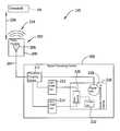
- FIG. 1is a block diagram of an exemplary power system.
- FIG. 2is a block diagram of an exemplary sensor assembly that may be used with the power system shown in FIG. 1 .
- FIG. 3is a front view of an exemplary emitter body that may be used with the sensor assembly shown in FIG. 2 .
- FIG. 4is a partial cut-away view of an exemplary microwave sensor probe that may be used with the sensor assembly shown in FIG. 2 .
- FIG. 1shows an exemplary power system 100 that includes a machine 102 .
- machine 102may be, but is not limited to only being, a wind turbine, a hydroelectric turbine, a gas turbine, or a compressor.
- machine 102may be any other machine used in a power system.
- machine 102rotates a drive shaft 104 coupled to a load 106 , such as a generator.
- drive shaft 104is at least partially supported by one or more bearings (not shown) housed within machine 102 and/or within load 106 .
- the bearingsmay be housed within a separate support structure 108 , such as a gearbox, or within any other structure or component that enables power system 100 to function as described herein.
- power system 100includes at least one sensor assembly 110 that measures and/or monitors at least one operating condition of machine 102 , of drive shaft 104 , of load 106 , and/or of any other component of power system 100 that enables system 100 to function as described herein.
- sensor assembly 110is a proximity sensor assembly 110 positioned in close proximity to drive shaft 104 for measuring and/or monitoring a distance (not shown in FIG. 1 ) defined between drive shaft 104 and sensor assembly 110 .
- sensor assembly 110uses microwave signals to measure a proximity of a component of power system 100 with respect to sensor assembly 110 .
- microwaverefers to a signal or a component that receives and/or transmits signals having one or more frequencies between about 300 megahertz (MHz) and about 300 gigahertz (GHz).
- sensor assembly 110may measure and/or monitor any other component of power system 100 , and/or may be any other sensor or transducer assembly that enables power system 100 to function as described herein.
- each sensor assembly 110is positioned in any location within power system 100 .
- at least one sensor assembly 110is coupled to a diagnostic system 112 for use in processing and/or analyzing one or more signals generated by sensor assemblies 110 .
- the operation of machine 102may cause one or more components of power system 100 , such as drive shaft 104 , to change position with respect to at least one sensor assembly 110 .
- vibrationsmay be induced to the components and/or the components may expand or contract as the operating temperature within power system 100 changes.
- sensor assemblies 110measure and/or monitor the proximity, position, and/or the amount of vibration of the components relative to each sensor assembly 110 and transmit a signal representative of the measured proximity, position, and/or the amount of vibration of the components (hereinafter referred to as a “proximity measurement signal”) to diagnostic system 112 for processing and/or analysis.
- FIG. 2is a schematic diagram of an exemplary sensor assembly 110 that may be used with power system 100 (shown in FIG. 1 ).
- sensor assembly 110includes a signal processing device 200 and a probe 202 coupled to signal processing device 200 via a data conduit 204 .
- probe 202includes an emitter 206 coupled to and/or positioned within a probe housing 208 .
- probe 202is a microwave probe 202 that includes a microwave emitter 206 .
- emitter 206has at least one resonant frequency within a microwave frequency range.
- signal processing device 200includes a directional coupling device 210 coupled to a transmission power detector 212 , to a reception power detector 214 , and to a signal conditioning device 216 .
- signal conditioning device 216includes a signal generator 218 , a subtractor 220 , and a linearizer 222 .
- Emitter 206emits an electromagnetic field 224 when a microwave signal is transmitted through emitter 206 .
- signal generator 218generates at least one electrical signal having a microwave frequency (hereinafter referred to as a “microwave signal”) that is equal to or approximately equal to the resonant frequency of emitter 206 .
- Signal generator 218transmits the microwave signal to directional coupling device 210 .
- Directional coupling device 210transmits the microwave signal to transmission power detector 212 and to emitter 206 .
- electromagnetic field 224is emitted from emitter 206 and out of probe housing 208 . If an object, such as a drive shaft 104 or another component of machine 102 (shown in FIG.
- electromagnetic field 224may be disrupted, for example, because of an induction and/or capacitive effect induced within the object that may cause at least a portion of electromagnetic field 224 to be inductively and/or capacitively coupled to the object as an electrical current and/or charge.
- emitter 206is detuned (i.e., a resonant frequency of emitter 206 is reduced and/or changed) and a loading is induced to emitter 206 .
- the loading induced to emitter 206causes a reflection of the microwave signal (hereinafter referred to as a “detuned loading signal”) to be transmitted through data conduit 204 to directional coupling device 210 .
- the detuned loading signalhas a lower power amplitude and/or a different phase than the power amplitude and/or the phase of the microwave signal.
- the power amplitude of the detuned loading signalis dependent upon the proximity of the object to emitter 206 .
- Directional coupling device 210transmits the detuned loading signal to reception power detector 214 .
- reception power detector 214determines an amount of power based on and/or contained within the detuned loading signal and transmits a signal representative of the detuned loading signal power to signal conditioning device 216 .
- transmission power detector 212determines an amount of power based on and/or contained within the microwave signal and transmits a signal representative of the microwave signal power to signal conditioning device 216 .
- subtractor 220receives the microwave signal power and the detuned loading signal power, and calculates a difference between the microwave signal power and the detuned loading signal power.
- Subtractor 220transmits a signal representative of the calculated difference (hereinafter referred to as a “power difference signal”) to linearizer 222 .
- an amplitude of the power difference signalis proportional, such as inversely or exponentially proportional, to a distance 226 defined between the object, such as drive shaft 104 , within electromagnetic field 224 and probe 202 and/or emitter 206 (i.e., distance 226 is known as the object proximity).
- the amplitude of the power difference signalmay at least partially exhibit a non-linear relationship with respect to the object proximity.
- linearizer 222transforms the power difference signal into a voltage output signal (i.e., the “proximity measurement signal”) that exhibits a substantially linear relationship between the object proximity and the amplitude of the proximity measurement signal. Moreover, in the exemplary embodiment, linearizer 222 transmits the proximity measurement signal to diagnostic system 112 (shown in FIG. 1 ) with a scale factor suitable for processing and/or analysis within diagnostic system 112 . In the exemplary embodiment, the proximity measurement signal has a scale factor of volts per millimeter. Alternatively, the proximity measurement signal may have any other scale factor that enables diagnostic system 112 and/or power system 100 to function as described herein.
- FIG. 3is a front view of an exemplary emitter body 300 that may be used with sensor assembly 110 (shown in FIG. 2 ).
- emitter body 300is positioned within, and/or is coupled to, probe housing 208 (shown in FIG. 2 ).
- emitter 206is coupled to emitter body 300
- at least one electromagnetic absorbent member 302is positioned relative to, and/or coupled to, probe 202 and/or emitter body 300 .
- a plurality of members 302include a first electromagnetic absorbent pad 304 and a second electromagnetic absorbent pad 306 .
- emitter body 300includes a front surface 308 and an opposing rear surface 310 .
- Emitter 206in the exemplary embodiment, is coupled to front surface 308 and extends radially outward from a center 312 of front surface 308 .
- emitter body 300is a substantially planar printed circuit board, and emitter 206 includes one or more traces or conductors 314 that are formed integrally with, and/or coupled to, front surface 308 .
- emitter 206 and/or emitter body 300may be configured and/or constructed in any other arrangement that enables sensor assembly 110 to function as described herein.
- conductors 314form a first arm 316 and a second arm 318 that each extend radially outward from center 312 .
- First arm 316includes a first end 320 positioned proximate to center 312 , and a second end 322 positioned radially outward from center 312 .
- Second arm 318includes a first end 324 positioned proximate to center 312 , and a second end 326 positioned radially outward from center 312 .
- first arm 316 and second arm 318are substantially coplanar with front surface 308 such that emitter 206 does not extend a substantial distance axially outward from front surface 308 .
- emitter 206 and/or emitter body 300may include any number of emitter arms and/or may be any shape that enables microwave sensor assembly 110 to function as described herein.
- Emitter body 300in the exemplary embodiment, includes first electromagnetic absorbent pad 304 and second electromagnetic absorbent pad 306 .
- first and second electromagnetic absorbent pads 304 and 306are manufactured from a dielectric loading material that has a high magnetic permeability.
- such materialmay include a plurality of metal fibers entrained within a resin, thermoplastic material, and/or a rubber-based material.
- first electromagnetic absorbent pad 304 and/or second electromagnetic absorbent pad 306may be manufactured from any other material that has a layered impedance structure, that has a high dielectric constant, such as greater than about 10, and/or that has a high magnetic permeability, such as greater than about 1.
- first and second electromagnetic absorbent pads 304 and 306are substantially cubical or are rectangular cuboids. First and second electromagnetic absorbent pads 304 and 306 are coupled to second ends 322 and 326 , respectively. Alternatively, first and/or second electromagnetic absorbent pads 304 and/or 306 may have any shape, and may be coupled to first arm 316 and/or to second arm 318 at any other position that enables emitter 206 to function as described herein.
- emitter 206has a substantially low impedance, such as approximately 50 ohms, proximate to center 312 .
- the impedance of arms 316 and 318increases until a maximum impedance is reached at second ends 322 and 326 .
- an impedance at second ends 322 and 326may approach infinity.
- at least a portion of a current transmitted through emitter 206is reflected back from second ends 322 and 326 towards first ends 320 and 324 . Accordingly, a standing wave may undesirably be created within emitter 206 .
- first and second electromagnetic absorbent pads 304 and 306facilitates reducing the amount of current reflected from second ends 322 and 326 .
- first and second electromagnetic absorbent pads 304 and 306facilitate reducing the effective impedance of emitter 206 at second ends 322 and 326 such that emitter 206 has a more uniform impedance from first ends 320 and 324 to second ends 322 and 326 . Accordingly, an increased amount of energy may be concentrated in a center (not shown) of electromagnetic field 224 compared to systems that do not include first and second electromagnetic absorbent pads 304 and 306 .
- FIG. 4is a partial cut-away view of an exemplary microwave probe 202 that may be used with sensor assembly 110 (shown in FIG. 2 ).
- probe 202includes emitter body 300 and emitter 206 including first and second emitter arms 316 and 318 (shown in FIG. 3 ).
- emitter body 300is coupled to, and/or is positioned within, probe housing 208 .
- Probe housing 208may be manufactured from a thermoplastic material and/or any other material that enables probe 202 to function as described herein.
- a plurality of electromagnetic absorbent members 302are positioned relative to, and/or are coupled to, probe 202 and/or emitter body 300 . More specifically, members 302 include first electromagnetic absorbent pad 304 , second electromagnetic absorbent pad 306 (both shown in FIG. 3 ), an electromagnetic absorbent disk 400 , and/or an electromagnetic absorbent shell 402 .
- a cavity 404is defined within probe housing 208 .
- data conduit 204extends through cavity 404 substantially along a centerline 406 of probe housing 208 .
- Data conduit 204is coupled to emitter 206 through rear surface 310 for use in transmitting and receiving signals to and from signal processing device 200 (shown in FIG. 2 ).
- electromagnetic absorbent disk 400is substantially circular and is coupled to rear surface 310 such that rear surface 310 is substantially covered by disk 400 .
- disk 400may be coupled to any portion of rear surface 310 that enables probe 202 to function as described herein.
- Disk 400in the exemplary embodiment, at least partially circumscribes data conduit 204 when conduit 204 is coupled to emitter 206 .
- electromagnetic absorbent shell 402is substantially cylindrical and is coupled to an inner surface 408 of probe housing 208 .
- Electromagnetic absorbent shell 402in the exemplary embodiment, is positioned about data conduit 204 such that shell 402 circumscribes at least a portion of cavity 404 .
- shell 402is substantially solid such that shell 402 fills at least a portion of cavity 404 .
- a downstream annular edge 410 of shell 402is coupled to rear surface 310 .
- annular edge 410is coupled to an upstream surface 412 of electromagnetic absorbent disk 400 .
- disk 400 and shell 402are manufactured from the same material as first and second electromagnetic absorbent pads 304 and 306 .
- disk 400 and/or shell 402may be manufactured from any other dielectric loading material and/or any material that has a layered impedance structure, that has a high dielectric constant, such as greater than about 10, and/or that has a high magnetic permeability, such as greater than about 1.
- upstreamrefers to a direction substantially along centerline 406 from emitter 206 towards a rear portion 414 of probe housing 208 .
- downstreamrefers to a direction substantially along centerline 406 from rear portion 414 towards emitter 206 .
- a microwave signalis transmitted to emitter 206 via data conduit 204 .
- the microwave signalis transmitted through first arm 316 and second arm 318 such that electromagnetic field 224 is emitted.
- First and second electromagnetic absorbent pads 304 and 306absorb and/or suppress a current that may be reflected from second ends 322 and 326 towards first ends 320 and 324 (all shown in FIG. 3 ). As such, an amount of common mode noise that might otherwise be reflected and/or transmitted back from emitter 206 to signal processing device 200 through data conduit 204 is reduced.
- Electromagnetic absorbent disk 400 and shell 402facilitate reducing and/or suppressing a portion (not shown) of electromagnetic field 224 that might otherwise radiate upstream from emitter 206 , i.e., through cavity 404 and/or through rear portion 414 .
- electromagnetic field 224is shaped and/or directed substantially downstream from emitter 206 . Because an increased amount of microwave energy may be directed downstream from emitter 206 , a detection range of sensor assembly 110 may be increased. Moreover, the proximity of an object to emitter 206 may be determined by sensor assembly 110 as described more fully above.
- Existing sensor assembliesmay be retrofitted with electromagnetic absorbent members 302 to adjust the operation of the sensor assemblies, as described herein.
- at least one electromagnetic absorbent member 302may be positioned relative to an emitter body. When a microwave signal is transmitted through the emitter such that an electromagnetic field is generated thereby, the electromagnetic absorbent members 302 may absorb a reflected current transmitted through the emitter and/or absorb a portion of the electromagnetic field that radiates backward (i.e., upstream) from the emitter.
- Probe 202includes first and second electromagnetic absorbent pads 304 and 306 that facilitate reducing and/or suppressing a current reflected through emitter 206 .
- emitter body 300does not need to include a ground plane to absorb the reflected current. Accordingly, more energy is enabled to be transmitted to electromagnetic field 224 than in prior art systems.
- probe 202includes an electromagnetic absorbent disk 400 and shell 402 that facilitate reducing and/or suppressing a portion of electromagnetic field 224 that may be directed at least partially upstream from emitter body 300 . As such, an increased amount of energy may be concentrated in the downstream portion of electromagnetic field 224 that is directed towards the measured object. Accordingly, a detection range of sensor assembly 110 is facilitated to be increased as compared to prior art systems.
- the above-described embodimentsprovide an efficient and cost-effective sensor assembly for use in measuring the proximity of a machine component to an emitter.
- the sensor assemblydrives the emitter with a microwave signal to generate an electromagnetic field.
- an objectsuch as a machine component
- the sensor assemblycalculates a proximity of the object to the emitter based on the loading induced to the emitter.
- a plurality of electromagnetic absorbent membersare positioned relative to, or are coupled to a probe that houses the emitter. The electromagnetic absorbent members facilitate reducing a current that may be reflected through the emitter, and facilitate reducing a portion of the electromagnetic field that may radiate upstream from the emitter. As such, a detection range and a measurement accuracy of the sensor assembly may be increased.
- a sensor assembly and methods for adjusting the operation of a sensorare described above in detail.
- the sensor assembly and methodsare not limited to the specific embodiments described herein, but rather, components of the sensor assembly and/or steps of the methods may be utilized independently and separately from other components and/or steps described herein.
- the sensor assemblymay also be used in combination with other measuring systems and methods, and is not limited to practice with only the power system as described herein. Rather, the exemplary embodiment can be implemented and utilized in connection with many other measurement and/or monitoring applications.
Landscapes
- Physics & Mathematics (AREA)
- General Physics & Mathematics (AREA)
- Length-Measuring Devices Using Wave Or Particle Radiation (AREA)
- Arrangements For Transmission Of Measured Signals (AREA)
- Measurement Of Length, Angles, Or The Like Using Electric Or Magnetic Means (AREA)
Abstract
Description
Claims (20)
Priority Applications (5)
| Application Number | Priority Date | Filing Date | Title |
|---|---|---|---|
| US12/951,633US8624603B2 (en) | 2010-11-22 | 2010-11-22 | Sensor assembly and methods of adjusting the operation of a sensor |
| EP11189220AEP2455730A1 (en) | 2010-11-22 | 2011-11-15 | Sensor Assembly And Methods Of Adjusting The Operation Of A Sensor |
| JP2011252143AJP2012112946A (en) | 2010-11-22 | 2011-11-18 | Sensor assembly and methods of adjusting operation of sensor |
| BRPI1104993-6ABRPI1104993A2 (en) | 2010-11-22 | 2011-11-21 | microwave sensor probe and microwave sensor assembly |
| CN201110393270XACN102565785A (en) | 2010-11-22 | 2011-11-22 | Sensor assembly and methods of adjusting the operation of a sensor |
Applications Claiming Priority (1)
| Application Number | Priority Date | Filing Date | Title |
|---|---|---|---|
| US12/951,633US8624603B2 (en) | 2010-11-22 | 2010-11-22 | Sensor assembly and methods of adjusting the operation of a sensor |
Publications (2)
| Publication Number | Publication Date |
|---|---|
| US20120126827A1 US20120126827A1 (en) | 2012-05-24 |
| US8624603B2true US8624603B2 (en) | 2014-01-07 |
Family
ID=45318812
Family Applications (1)
| Application Number | Title | Priority Date | Filing Date |
|---|---|---|---|
| US12/951,633Active2031-11-29US8624603B2 (en) | 2010-11-22 | 2010-11-22 | Sensor assembly and methods of adjusting the operation of a sensor |
Country Status (5)
| Country | Link |
|---|---|
| US (1) | US8624603B2 (en) |
| EP (1) | EP2455730A1 (en) |
| JP (1) | JP2012112946A (en) |
| CN (1) | CN102565785A (en) |
| BR (1) | BRPI1104993A2 (en) |
Cited By (2)
| Publication number | Priority date | Publication date | Assignee | Title |
|---|---|---|---|---|
| US11156455B2 (en) | 2018-09-26 | 2021-10-26 | General Electric Company | System and method for measuring clearance gaps between rotating and stationary components of a turbomachine |
| US20220403753A1 (en)* | 2019-12-05 | 2022-12-22 | Siemens Energy, Inc. | Turbine blade health monitoring system for identifying cracks |
Families Citing this family (1)
| Publication number | Priority date | Publication date | Assignee | Title |
|---|---|---|---|---|
| US8482456B2 (en)* | 2010-12-16 | 2013-07-09 | General Electric Company | Sensor assembly and method of measuring the proximity of a machine component to an emitter |
Citations (67)
| Publication number | Priority date | Publication date | Assignee | Title |
|---|---|---|---|---|
| US4045727A (en) | 1976-03-15 | 1977-08-30 | General Electric Company | Microwave proximity detector |
| US4313118A (en) | 1980-06-30 | 1982-01-26 | Calvin Noel M | Microwave proximity sensor |
| US4346383A (en) | 1979-08-04 | 1982-08-24 | Emi Limited | Checking the location of moving parts in a machine |
| US4384819A (en) | 1979-12-11 | 1983-05-24 | Smiths Industries Public Limited Company | Proximity sensing |
| US4525720A (en) | 1982-10-15 | 1985-06-25 | The United States Of America As Represented By The Secretary Of The Navy | Integrated spiral antenna and printed circuit balun |
| US4652864A (en) | 1982-07-26 | 1987-03-24 | Calvin Noel M | Microwave proximity sensor |
| US4845422A (en) | 1986-12-24 | 1989-07-04 | General Electric Company | Microwave proximity sensor |
| US4862061A (en) | 1986-12-24 | 1989-08-29 | General Electric Company | Microwave proximity sensor |
| US5097227A (en) | 1990-10-09 | 1992-03-17 | Texas Instruments Incorporated | Microwave oscillator position sensor |
| US5110216A (en)* | 1989-03-30 | 1992-05-05 | Luxtron Corporation | Fiberoptic techniques for measuring the magnitude of local microwave fields and power |
| US5227667A (en) | 1989-01-10 | 1993-07-13 | Omron Corporation | Microwave proximity switch |
| US5334969A (en) | 1991-07-10 | 1994-08-02 | Alpine Electronics, Inc. | Vehicle security system with controller proximity sensor |
| US5459397A (en) | 1992-11-23 | 1995-10-17 | Spillman, Jr.; William B. | Speed sensor for rotatable shaft using shaft mounted antenna |
| US5459405A (en) | 1991-05-22 | 1995-10-17 | Wolff Controls Corp. | Method and apparatus for sensing proximity of an object using near-field effects |
| US5506515A (en) | 1994-07-20 | 1996-04-09 | Cascade Microtech, Inc. | High-frequency probe tip assembly |
| US5670886A (en) | 1991-05-22 | 1997-09-23 | Wolf Controls Corporation | Method and apparatus for sensing proximity or position of an object using near-field effects |
| US5801530A (en) | 1995-04-17 | 1998-09-01 | Namco Controls Corporation | Proximity sensor having a non-ferrous metal shield for enhanced sensing range |
| US5818242A (en) | 1996-05-08 | 1998-10-06 | United Technologies Corporation | Microwave recess distance and air-path clearance sensor |
| US5854994A (en) | 1996-08-23 | 1998-12-29 | Csi Technology, Inc. | Vibration monitor and transmission system |
| US5963034A (en) | 1996-09-19 | 1999-10-05 | Ramar Corporation | Electro-optic electromagnetic field sensor system with optical bias adjustment |
| US5992237A (en) | 1997-07-22 | 1999-11-30 | Skf Condition Monitoring, Inc. | Digital vibration coupling stud |
| US6043774A (en) | 1998-03-25 | 2000-03-28 | Honeywell Inc. | Near-range proximity sensor having a fast-tracking analog |
| US6118287A (en) | 1997-12-09 | 2000-09-12 | Boll; Gregory George | Probe tip structure |
| US6227703B1 (en) | 1998-12-30 | 2001-05-08 | Adaptive Instruments Corporation | Variable length sensor probe system |
| US6261247B1 (en) | 1998-12-31 | 2001-07-17 | Ball Semiconductor, Inc. | Position sensing system |
| US6320550B1 (en) | 1998-04-06 | 2001-11-20 | Vortekx, Inc. | Contrawound helical antenna |
| US6407562B1 (en) | 1999-07-29 | 2002-06-18 | Agilent Technologies, Inc. | Probe tip terminating device providing an easily changeable feed-through termination |
| US6437751B1 (en) | 2000-08-15 | 2002-08-20 | West Virginia University | Contrawound antenna |
| US6445995B1 (en) | 2001-01-26 | 2002-09-03 | General Electric Company | Vibration sensing in gas turbine engine |
| US6462561B1 (en) | 2000-07-14 | 2002-10-08 | The United States Of America As Represented By The Secretary Of The Navy | Standoff distance variation compensator and equalizer |
| US20030155934A1 (en)* | 2000-09-20 | 2003-08-21 | Moreland Robert L. | Apertured probes for localized measurements of a material's complex permittivity and fabrication method |
| US6620057B1 (en) | 1999-04-15 | 2003-09-16 | Flite Traxx, Inc. | System for locating golf balls |
| US6750621B2 (en) | 2001-09-10 | 2004-06-15 | Sauer-Danfoss Inc. | Method and system for non-contact sensing of motion of a roller drum |
| US6778132B2 (en) | 2002-02-13 | 2004-08-17 | I F M Electronic Gmbh | Microwave sensor |
| US6864796B2 (en) | 1999-09-15 | 2005-03-08 | Ilife Solutions, Inc. | Systems within a communication device for evaluating movement of a body and methods of operating the same |
| US6878147B2 (en) | 2001-11-02 | 2005-04-12 | Vivant Medical, Inc. | High-strength microwave antenna assemblies |
| US6984994B2 (en) | 2000-03-14 | 2006-01-10 | Isis Innovation Limited | Position and electromagnetic field sensor |
| US7073384B1 (en) | 1999-08-23 | 2006-07-11 | Stevens Institute Of Technology | Method and apparatus for remote measurement of vibration and properties of objects |
| US7079029B2 (en) | 2001-10-30 | 2006-07-18 | Optex Co., Ltd. | Dual-frequency microwave sensor |
| US7079030B2 (en) | 2003-05-07 | 2006-07-18 | Optex Co., Ltd. | Microwave sensor |
| US7119737B2 (en) | 2001-10-19 | 2006-10-10 | Optex Co., Ltd. | Microwave sensor |
| US7159774B2 (en) | 2003-04-30 | 2007-01-09 | The United States Of America As Represented By The Administrator Of The National Aeronautics And Space Administration | Magnetic field response measurement acquisition system |
| US20070024508A1 (en) | 2005-07-26 | 2007-02-01 | Lg Electronics Inc. | Portable terminal having antenna apparatus |
| US7176829B2 (en) | 2004-02-04 | 2007-02-13 | Optex Co., Ltd. | Microwave sensor |
| US7206719B2 (en) | 2003-07-07 | 2007-04-17 | Dofasco Inc. | Diagnostic method for predicting maintenance requirements in rotating equipment |
| US7215111B2 (en) | 2004-08-26 | 2007-05-08 | Hitachi Cable, Ltd. | Magnetic motion sensor |
| US7215252B2 (en) | 2004-06-16 | 2007-05-08 | Hamilton Sundstrand Corporation | Proximity sensor |
| US7250920B1 (en) | 2004-09-29 | 2007-07-31 | The United States Of America As Represented By The Secrtary Of The Navy | Multi-purpose electromagnetic radiation interface system and method |
| US7256376B2 (en) | 2004-03-30 | 2007-08-14 | Optex Co., Ltd. | Microwave sensor and mutual interference preventing system between microwave sensors |
| US7274189B2 (en) | 2004-09-09 | 2007-09-25 | Rockwell Automation Technologies, Inc. | Sensor and method |
| WO2007147629A1 (en) | 2006-06-23 | 2007-12-27 | Fractus, S.A. | Chip module, sim card, wireless device and wireless communication method |
| WO2008069750A1 (en) | 2006-12-08 | 2008-06-12 | Perlos Oyj | Antenna for mobile terminal unit |
| EP1942556A1 (en) | 2006-12-29 | 2008-07-09 | LG Electronics Inc. | Antenna and electronic equipment having the same |
| US7423934B1 (en) | 2005-08-09 | 2008-09-09 | Uzes Charles A | System for detecting, tracking, and reconstructing signals in spectrally competitive environments |
| US7455495B2 (en) | 2005-08-16 | 2008-11-25 | United Technologies Corporation | Systems and methods for monitoring thermal growth and controlling clearances, and maintaining health of turbo machinery applications |
| US20080303513A1 (en) | 2007-06-08 | 2008-12-11 | Kelsey-Hayes Company | Wireless active wheel speed sensor |
| US7483800B2 (en) | 2006-06-01 | 2009-01-27 | Radatec, Inc. | Peak detection and clutter reduction for a microwave sensor |
| US7492165B2 (en) | 2005-08-11 | 2009-02-17 | Festo Ag & Co. | Position detecting device with a microwave antenna arrangement |
| US20090102451A1 (en) | 2004-04-20 | 2009-04-23 | International Business Machines Corporation | Method and structure for variable pitch microwave probe assembly |
| US7532155B2 (en)* | 2006-04-10 | 2009-05-12 | Rosemount Tank Radar Ab | Radar level gauging system |
| US7532151B2 (en) | 2003-10-17 | 2009-05-12 | Aisin Seiki Kabushiki Kaisha | Proximity sensor |
| US7541995B1 (en) | 2007-09-25 | 2009-06-02 | The United States Of America As Represented By The Secretary Of The Navy | Electromagnetic signal proximity detection systems and methods |
| US7554324B2 (en) | 2003-10-28 | 2009-06-30 | Honeywell International Inc. | Turbine blade proximity sensor and control system |
| US20090243915A1 (en) | 2008-03-31 | 2009-10-01 | Yoshiteru Nishizato | Microwave sensor apparatus and microwave sensor system |
| US7604413B2 (en) | 2004-06-25 | 2009-10-20 | Ntn Corporation | Wheel support bearing assembly with built-in load sensor |
| US20100125269A1 (en) | 2008-10-21 | 2010-05-20 | Microcube, Limited Liability Corporation | Microwave treatment devices and methods |
| US20100211334A1 (en) | 2009-02-18 | 2010-08-19 | General Electric Company | Methods and Systems for Monitoring Stator Winding Vibration |
Family Cites Families (2)
| Publication number | Priority date | Publication date | Assignee | Title |
|---|---|---|---|---|
| GB9808762D0 (en)* | 1998-04-25 | 1998-06-24 | Marconi Gec Ltd | Modulated reflector circuit |
| AU2003263746A1 (en)* | 2002-07-03 | 2004-01-23 | Tokyo Electron Limited | Method and apparatus for non-invasive measurement and analysis of semiconductor process parameters |
- 2010
- 2010-11-22USUS12/951,633patent/US8624603B2/enactiveActive
- 2011
- 2011-11-15EPEP11189220Apatent/EP2455730A1/ennot_activeWithdrawn
- 2011-11-18JPJP2011252143Apatent/JP2012112946A/enactivePending
- 2011-11-21BRBRPI1104993-6Apatent/BRPI1104993A2/ennot_activeApplication Discontinuation
- 2011-11-22CNCN201110393270XApatent/CN102565785A/enactivePending
Patent Citations (70)
| Publication number | Priority date | Publication date | Assignee | Title |
|---|---|---|---|---|
| US4045727A (en) | 1976-03-15 | 1977-08-30 | General Electric Company | Microwave proximity detector |
| US4346383A (en) | 1979-08-04 | 1982-08-24 | Emi Limited | Checking the location of moving parts in a machine |
| US4384819A (en) | 1979-12-11 | 1983-05-24 | Smiths Industries Public Limited Company | Proximity sensing |
| US4313118A (en) | 1980-06-30 | 1982-01-26 | Calvin Noel M | Microwave proximity sensor |
| US4652864A (en) | 1982-07-26 | 1987-03-24 | Calvin Noel M | Microwave proximity sensor |
| US4525720A (en) | 1982-10-15 | 1985-06-25 | The United States Of America As Represented By The Secretary Of The Navy | Integrated spiral antenna and printed circuit balun |
| US4845422A (en) | 1986-12-24 | 1989-07-04 | General Electric Company | Microwave proximity sensor |
| US4862061A (en) | 1986-12-24 | 1989-08-29 | General Electric Company | Microwave proximity sensor |
| US5227667A (en) | 1989-01-10 | 1993-07-13 | Omron Corporation | Microwave proximity switch |
| US5110216A (en)* | 1989-03-30 | 1992-05-05 | Luxtron Corporation | Fiberoptic techniques for measuring the magnitude of local microwave fields and power |
| US5097227A (en) | 1990-10-09 | 1992-03-17 | Texas Instruments Incorporated | Microwave oscillator position sensor |
| US5459405A (en) | 1991-05-22 | 1995-10-17 | Wolff Controls Corp. | Method and apparatus for sensing proximity of an object using near-field effects |
| US5670886A (en) | 1991-05-22 | 1997-09-23 | Wolf Controls Corporation | Method and apparatus for sensing proximity or position of an object using near-field effects |
| US5334969A (en) | 1991-07-10 | 1994-08-02 | Alpine Electronics, Inc. | Vehicle security system with controller proximity sensor |
| US5459397A (en) | 1992-11-23 | 1995-10-17 | Spillman, Jr.; William B. | Speed sensor for rotatable shaft using shaft mounted antenna |
| US5506515A (en) | 1994-07-20 | 1996-04-09 | Cascade Microtech, Inc. | High-frequency probe tip assembly |
| US5801530A (en) | 1995-04-17 | 1998-09-01 | Namco Controls Corporation | Proximity sensor having a non-ferrous metal shield for enhanced sensing range |
| US5818242A (en) | 1996-05-08 | 1998-10-06 | United Technologies Corporation | Microwave recess distance and air-path clearance sensor |
| US5854994A (en) | 1996-08-23 | 1998-12-29 | Csi Technology, Inc. | Vibration monitor and transmission system |
| US5963034A (en) | 1996-09-19 | 1999-10-05 | Ramar Corporation | Electro-optic electromagnetic field sensor system with optical bias adjustment |
| US5992237A (en) | 1997-07-22 | 1999-11-30 | Skf Condition Monitoring, Inc. | Digital vibration coupling stud |
| US6118287A (en) | 1997-12-09 | 2000-09-12 | Boll; Gregory George | Probe tip structure |
| US6043774A (en) | 1998-03-25 | 2000-03-28 | Honeywell Inc. | Near-range proximity sensor having a fast-tracking analog |
| US6320550B1 (en) | 1998-04-06 | 2001-11-20 | Vortekx, Inc. | Contrawound helical antenna |
| US6227703B1 (en) | 1998-12-30 | 2001-05-08 | Adaptive Instruments Corporation | Variable length sensor probe system |
| US6261247B1 (en) | 1998-12-31 | 2001-07-17 | Ball Semiconductor, Inc. | Position sensing system |
| US6620057B1 (en) | 1999-04-15 | 2003-09-16 | Flite Traxx, Inc. | System for locating golf balls |
| US6407562B1 (en) | 1999-07-29 | 2002-06-18 | Agilent Technologies, Inc. | Probe tip terminating device providing an easily changeable feed-through termination |
| US7073384B1 (en) | 1999-08-23 | 2006-07-11 | Stevens Institute Of Technology | Method and apparatus for remote measurement of vibration and properties of objects |
| US6864796B2 (en) | 1999-09-15 | 2005-03-08 | Ilife Solutions, Inc. | Systems within a communication device for evaluating movement of a body and methods of operating the same |
| US6984994B2 (en) | 2000-03-14 | 2006-01-10 | Isis Innovation Limited | Position and electromagnetic field sensor |
| US6462561B1 (en) | 2000-07-14 | 2002-10-08 | The United States Of America As Represented By The Secretary Of The Navy | Standoff distance variation compensator and equalizer |
| US6437751B1 (en) | 2000-08-15 | 2002-08-20 | West Virginia University | Contrawound antenna |
| US20030155934A1 (en)* | 2000-09-20 | 2003-08-21 | Moreland Robert L. | Apertured probes for localized measurements of a material's complex permittivity and fabrication method |
| US6445995B1 (en) | 2001-01-26 | 2002-09-03 | General Electric Company | Vibration sensing in gas turbine engine |
| US6750621B2 (en) | 2001-09-10 | 2004-06-15 | Sauer-Danfoss Inc. | Method and system for non-contact sensing of motion of a roller drum |
| US7119737B2 (en) | 2001-10-19 | 2006-10-10 | Optex Co., Ltd. | Microwave sensor |
| US7079029B2 (en) | 2001-10-30 | 2006-07-18 | Optex Co., Ltd. | Dual-frequency microwave sensor |
| US6878147B2 (en) | 2001-11-02 | 2005-04-12 | Vivant Medical, Inc. | High-strength microwave antenna assemblies |
| US7318824B2 (en) | 2001-11-02 | 2008-01-15 | Vivant Medical, Inc. | High-strength microwave antenna assemblies |
| US7527623B2 (en) | 2001-11-02 | 2009-05-05 | Vivant Medical, Inc. | High-strength microwave antenna assemblies |
| US6778132B2 (en) | 2002-02-13 | 2004-08-17 | I F M Electronic Gmbh | Microwave sensor |
| US7159774B2 (en) | 2003-04-30 | 2007-01-09 | The United States Of America As Represented By The Administrator Of The National Aeronautics And Space Administration | Magnetic field response measurement acquisition system |
| US7079030B2 (en) | 2003-05-07 | 2006-07-18 | Optex Co., Ltd. | Microwave sensor |
| US7206719B2 (en) | 2003-07-07 | 2007-04-17 | Dofasco Inc. | Diagnostic method for predicting maintenance requirements in rotating equipment |
| US7532151B2 (en) | 2003-10-17 | 2009-05-12 | Aisin Seiki Kabushiki Kaisha | Proximity sensor |
| US7554324B2 (en) | 2003-10-28 | 2009-06-30 | Honeywell International Inc. | Turbine blade proximity sensor and control system |
| US7176829B2 (en) | 2004-02-04 | 2007-02-13 | Optex Co., Ltd. | Microwave sensor |
| US7256376B2 (en) | 2004-03-30 | 2007-08-14 | Optex Co., Ltd. | Microwave sensor and mutual interference preventing system between microwave sensors |
| US20090102451A1 (en) | 2004-04-20 | 2009-04-23 | International Business Machines Corporation | Method and structure for variable pitch microwave probe assembly |
| US7215252B2 (en) | 2004-06-16 | 2007-05-08 | Hamilton Sundstrand Corporation | Proximity sensor |
| US7604413B2 (en) | 2004-06-25 | 2009-10-20 | Ntn Corporation | Wheel support bearing assembly with built-in load sensor |
| US7215111B2 (en) | 2004-08-26 | 2007-05-08 | Hitachi Cable, Ltd. | Magnetic motion sensor |
| US7274189B2 (en) | 2004-09-09 | 2007-09-25 | Rockwell Automation Technologies, Inc. | Sensor and method |
| US7250920B1 (en) | 2004-09-29 | 2007-07-31 | The United States Of America As Represented By The Secrtary Of The Navy | Multi-purpose electromagnetic radiation interface system and method |
| US20070024508A1 (en) | 2005-07-26 | 2007-02-01 | Lg Electronics Inc. | Portable terminal having antenna apparatus |
| US7423934B1 (en) | 2005-08-09 | 2008-09-09 | Uzes Charles A | System for detecting, tracking, and reconstructing signals in spectrally competitive environments |
| US7492165B2 (en) | 2005-08-11 | 2009-02-17 | Festo Ag & Co. | Position detecting device with a microwave antenna arrangement |
| US7455495B2 (en) | 2005-08-16 | 2008-11-25 | United Technologies Corporation | Systems and methods for monitoring thermal growth and controlling clearances, and maintaining health of turbo machinery applications |
| US7532155B2 (en)* | 2006-04-10 | 2009-05-12 | Rosemount Tank Radar Ab | Radar level gauging system |
| US7483800B2 (en) | 2006-06-01 | 2009-01-27 | Radatec, Inc. | Peak detection and clutter reduction for a microwave sensor |
| WO2007147629A1 (en) | 2006-06-23 | 2007-12-27 | Fractus, S.A. | Chip module, sim card, wireless device and wireless communication method |
| US20100019038A1 (en)* | 2006-06-23 | 2010-01-28 | Fractus, S.A. | Chip module, sim card, wireless device and wireless communication method |
| WO2008069750A1 (en) | 2006-12-08 | 2008-06-12 | Perlos Oyj | Antenna for mobile terminal unit |
| EP1942556A1 (en) | 2006-12-29 | 2008-07-09 | LG Electronics Inc. | Antenna and electronic equipment having the same |
| US20080303513A1 (en) | 2007-06-08 | 2008-12-11 | Kelsey-Hayes Company | Wireless active wheel speed sensor |
| US7541995B1 (en) | 2007-09-25 | 2009-06-02 | The United States Of America As Represented By The Secretary Of The Navy | Electromagnetic signal proximity detection systems and methods |
| US20090243915A1 (en) | 2008-03-31 | 2009-10-01 | Yoshiteru Nishizato | Microwave sensor apparatus and microwave sensor system |
| US20100125269A1 (en) | 2008-10-21 | 2010-05-20 | Microcube, Limited Liability Corporation | Microwave treatment devices and methods |
| US20100211334A1 (en) | 2009-02-18 | 2010-08-19 | General Electric Company | Methods and Systems for Monitoring Stator Winding Vibration |
Non-Patent Citations (1)
| Title |
|---|
| Search Report and Written Opinion from corresponding EP Application No. 11189220.4-2213 dated Mar. 15, 2012. |
Cited By (3)
| Publication number | Priority date | Publication date | Assignee | Title |
|---|---|---|---|---|
| US11156455B2 (en) | 2018-09-26 | 2021-10-26 | General Electric Company | System and method for measuring clearance gaps between rotating and stationary components of a turbomachine |
| US20220403753A1 (en)* | 2019-12-05 | 2022-12-22 | Siemens Energy, Inc. | Turbine blade health monitoring system for identifying cracks |
| US11802491B2 (en)* | 2019-12-05 | 2023-10-31 | Siemens Energy, Inc. | Turbine blade health monitoring system for identifying cracks |
Also Published As
| Publication number | Publication date |
|---|---|
| CN102565785A (en) | 2012-07-11 |
| US20120126827A1 (en) | 2012-05-24 |
| EP2455730A1 (en) | 2012-05-23 |
| JP2012112946A (en) | 2012-06-14 |
| BRPI1104993A2 (en) | 2013-03-19 |
Similar Documents
| Publication | Publication Date | Title |
|---|---|---|
| US20120126794A1 (en) | Sensor Assembly And Methods Of Assembling A Sensor Probe | |
| US8829923B2 (en) | Proximity sensor assembly and inspection system | |
| US20130320997A1 (en) | Sensor system and antenna for use in a sensor system | |
| JP2012112943A (en) | Sensor assembly and methods of measuring proximity of machine component to sensor | |
| US20120326730A1 (en) | Sensor assembly and microwave emitter for use in a sensor assembly | |
| US8624603B2 (en) | Sensor assembly and methods of adjusting the operation of a sensor | |
| US8593156B2 (en) | Sensor assembly and microwave emitter for use in a sensor assembly | |
| US8854052B2 (en) | Sensor assembly and method of measuring the proximity of a machine component to a sensor | |
| US20130119977A1 (en) | Sensing element for sensor assembly | |
| US8531191B2 (en) | Sensor assembly and methods of measuring a proximity of a machine component to a sensor | |
| US8674707B2 (en) | Sensor assemblies used to detect the proximity of a material to a microwave element | |
| EP2466253B1 (en) | Sensor assembly and method of measuring the proximity of a machine component to an emitter | |
| US20120126825A1 (en) | Sensor assembly and methods of measuring the proximity of a component to an emitter | |
| US8742769B2 (en) | Sensor probe and methods of assembling same |
Legal Events
| Date | Code | Title | Description |
|---|---|---|---|
| AS | Assignment | Owner name:GENERAL ELECTRIC COMPANY, NEW YORK Free format text:ASSIGNMENT OF ASSIGNORS INTEREST;ASSIGNORS:LEE, YONGJAE;SHEIKMAN, BORIS LEONID;GO, STEVEN;SIGNING DATES FROM 20101116 TO 20101118;REEL/FRAME:025393/0325 | |
| FEPP | Fee payment procedure | Free format text:PAYOR NUMBER ASSIGNED (ORIGINAL EVENT CODE: ASPN); ENTITY STATUS OF PATENT OWNER: LARGE ENTITY | |
| STCF | Information on status: patent grant | Free format text:PATENTED CASE | |
| FPAY | Fee payment | Year of fee payment:4 | |
| AS | Assignment | Owner name:BAKER HUGHES, A GE COMPANY, LLC, TEXAS Free format text:ASSIGNMENT OF ASSIGNORS INTEREST;ASSIGNOR:GENERAL ELECTRIC COMPANY;REEL/FRAME:051698/0346 Effective date:20170703 | |
| MAFP | Maintenance fee payment | Free format text:PAYMENT OF MAINTENANCE FEE, 8TH YEAR, LARGE ENTITY (ORIGINAL EVENT CODE: M1552); ENTITY STATUS OF PATENT OWNER: LARGE ENTITY Year of fee payment:8 | |
| AS | Assignment | Owner name:BAKER HUGHES, A GE COMPANY, LLC, TEXAS Free format text:CHANGE OF NAME;ASSIGNOR:BAKER HUGHES, A GE COMPANY, LLC;REEL/FRAME:062748/0526 Effective date:20200413 | |
| MAFP | Maintenance fee payment | Free format text:PAYMENT OF MAINTENANCE FEE, 12TH YEAR, LARGE ENTITY (ORIGINAL EVENT CODE: M1553); ENTITY STATUS OF PATENT OWNER: LARGE ENTITY Year of fee payment:12 |