US8623687B2 - Methods of forming thermoelectric devices including conductive posts and/or different solder materials and related methods and structures - Google Patents
Methods of forming thermoelectric devices including conductive posts and/or different solder materials and related methods and structuresDownload PDFInfo
- Publication number
- US8623687B2 US8623687B2US11/472,032US47203206AUS8623687B2US 8623687 B2US8623687 B2US 8623687B2US 47203206 AUS47203206 AUS 47203206AUS 8623687 B2US8623687 B2US 8623687B2
- Authority
- US
- United States
- Prior art keywords
- layer
- thermoelectric
- electrically conductive
- header
- solder
- Prior art date
- Legal status (The legal status is an assumption and is not a legal conclusion. Google has not performed a legal analysis and makes no representation as to the accuracy of the status listed.)
- Active, expires
Links
Images


Classifications
- H—ELECTRICITY
- H10—SEMICONDUCTOR DEVICES; ELECTRIC SOLID-STATE DEVICES NOT OTHERWISE PROVIDED FOR
- H10N—ELECTRIC SOLID-STATE DEVICES NOT OTHERWISE PROVIDED FOR
- H10N10/00—Thermoelectric devices comprising a junction of dissimilar materials, i.e. devices exhibiting Seebeck or Peltier effects
- H10N10/10—Thermoelectric devices comprising a junction of dissimilar materials, i.e. devices exhibiting Seebeck or Peltier effects operating with only the Peltier or Seebeck effects
- H10N10/17—Thermoelectric devices comprising a junction of dissimilar materials, i.e. devices exhibiting Seebeck or Peltier effects operating with only the Peltier or Seebeck effects characterised by the structure or configuration of the cell or thermocouple forming the device
- H—ELECTRICITY
- H10—SEMICONDUCTOR DEVICES; ELECTRIC SOLID-STATE DEVICES NOT OTHERWISE PROVIDED FOR
- H10N—ELECTRIC SOLID-STATE DEVICES NOT OTHERWISE PROVIDED FOR
- H10N10/00—Thermoelectric devices comprising a junction of dissimilar materials, i.e. devices exhibiting Seebeck or Peltier effects
- H10N10/80—Constructional details
- H10N10/81—Structural details of the junction
- H10N10/817—Structural details of the junction the junction being non-separable, e.g. being cemented, sintered or soldered
- H—ELECTRICITY
- H10—SEMICONDUCTOR DEVICES; ELECTRIC SOLID-STATE DEVICES NOT OTHERWISE PROVIDED FOR
- H10N—ELECTRIC SOLID-STATE DEVICES NOT OTHERWISE PROVIDED FOR
- H10N10/00—Thermoelectric devices comprising a junction of dissimilar materials, i.e. devices exhibiting Seebeck or Peltier effects
- H10N10/01—Manufacture or treatment
Definitions
- the present inventionrelates to the field of electronics, and more particularly to thermoelectric device structures and related methods.
- Thermoelectric materialsmay be used to provide cooling and/or power generation according to the Peltier effect.
- Thermoelectric materialsare discussed, for example, in the reference by Venkatasubramanian et al. entitled “ Phonon - Blocking Electron - Transmitting Structures ” (18 th International Conference On Thermoelectrics, 1999), the disclosure of which is hereby incorporated herein in its entirety by reference.
- thermoelectric coolingmay be expected to improve the performance of electronics and sensors such as, for example, RF receiver front-ends, infrared (IR) imagers, ultra-sensitive magnetic signature sensors, and/or superconducting electronics.
- Bulk thermoelectric materials typically based on p-Bi x Sb 2-x Te 3 and n-Bi 2 Te 3-x Se x alloysmay have figures-of-merit (ZT) and/or coefficients of performance (COP) which result in relatively poor thermoelectric device performance.
- thermoelectric devicesmay use alloys, such as p-Bi x Sb 2-x Te 3-y Se y (x ⁇ 0.5, y ⁇ 0.12) and n-Bi 2 (Se y Te 1-y ) 3 (y ⁇ 0.05) for the 200 degree K to 400 degree K temperature range.
- K Lmay be reduced more strongly than ⁇ leading to enhanced ZT.
- thermoelectric materialsthere continues to exist a need in the art for improved thermoelectric device structures and assembly methods.
- a method of forming a thermoelectric devicemay include forming a first electrically conductive trace, and bonding a thermoelectric element to the first electrically conductive trace. After bonding the thermoelectric element to the first electrically conductive trace, a metal post may be formed on the thermoelectric element so that the thermoelectric element is between the first electrically conductive trace and the metal post. After forming the metal post, the metal post may be bonded to a second electrically conductive trace so that the metal post is between the second electrically conductive trace and the thermoelectric element.
- Bonding the thermoelectric element to the first electrically conductive tracemay include providing a first solder material between the thermoelectric element and the first electrically conductive trace and reflowing the first solder material.
- Bonding the metal post to the second electrically conductive tracemay include providing a second solder material between the metal post and the second electrically conductive trace and reflowing the second solder material.
- the first and second solder materialsmay be different. More particularly, the first solder material may have a first reflow temperature, and the second solder material may have a second reflow temperature less than the first reflow temperature.
- the metal postmay have a thickness of at least about 15 ⁇ m (micrometers) between the thermoelectric element and the second electrically conductive trace.
- the thermoelectric elementmay be a first thermoelectric element, and the metal post may be a first metal post.
- a second thermoelectric elementmay be bonded to the first electrically conductive trace, and the first and second thermoelectric elements may have different conductivity types.
- a second metal postmay be formed on the second thermoelectric element so that the second thermoelectric element is between the second metal post and the first electrically conductive trace.
- the second metal postmay be bonded to a third electrically conductive trace so that the metal post is between the third electrically conductive trace and the second metal post.
- Forming the first electrically conductive tracemay include forming the first electrically conductive trace on a first header.
- a third electrically conductive tracemay be formed on a second header before bonding the second metal post to the third electrically conductive trace.
- the thermoelectric elementmay include a superlattice of alternating layers of at least two different thermoelectric materials.
- a method of forming a thermoelectric devicemay include forming a first electrically conductive trace.
- a thermoelectric elementmay be bonded to the first electrically conductive trace using a first solder layer having a first reflow temperature so that the first solder layer is between the thermoelectric element and the first electrically conductive trace.
- the thermoelectric elementmay be bonded to a second electrically conductive trace using a second solder layer having a second reflow temperature different than the first reflow temperature so that the thermoelectric element is between the first and second electrically conductive traces.
- the first and second solder layerscomprise different materials.
- Bonding the thermoelectric element to the first electrically conductive tracemay precede bonding the thermoelectric element to the second electrically conductive trace, and the first reflow temperature may be greater than the second reflow temperature.
- a metal postmay be formed on the thermoelectric element.
- bonding the thermoelectric element to the second electrically conductive tracemay include bonding the metal post to the second electrically conductive trace using the second solder layer so that the metal post is between the thermoelectric element and the second solder layer.
- the metal postmay have a thickness of at least about 15 ⁇ m (micrometers).
- the thermoelectric elementmay include a first thermoelectric element.
- a second thermoelectric elementmay be bonded to the first electrically conductive trace using a third solder layer, and reflow temperatures of the first and third solder layers may be the same.
- the first and second thermoelectric elementshave different conductivity types.
- the second thermoelectric elementmay be bonded to a third electrically conductive trace using a fourth solder layer so that the second thermoelectric element is between the first and third electrically conductive traces.
- Forming the first electrically conductive tracemay include forming the first electrically conductive trace on a header.
- the second electrically conductive tracemay be formed on a second header before bonding the thermoelectric element to the second electrically conductive trace.
- the thermoelectric elementmay include a superlattice of alternating layers of at least two different thermoelectric materials.
- a method of forming a thermoelectric devicemay include forming a thermoelectric element on a substrate wherein the thermoelectric element and the substrate have aligned crystal structures, and wherein the thermoelectric element and the substrate comprise different materials.
- An electrically conductive tracemay be formed on a header. After forming the thermoelectric element and after forming the electrically conductive trace, the thermoelectric element may be bonded to the electrically conductive trace so that the thermoelectric element is between the electrically conductive trace and the substrate.
- thermoelectric elementmay be a first thermoelectric element and wherein the substrate may be a first substrate.
- a second thermoelectric elementmay be formed on a second substrate.
- the second thermoelectric element and the substratemay have aligned crystal structures, the second thermoelectric element and the second substrate may include different materials, and the first and second thermoelectric elements may have opposite conductivity types.
- the second thermoelectric elementmay be bonded to the electrically conductive trace so that the second thermoelectric element is between the electrically conductive trace and the second substrate.
- Bonding the thermoelectric elementmay include bonding the thermoelectric element to the electrically conductive trace using a solder layer.
- the thermoelectric elementmay include a superlattice of alternating layers of at least two different thermoelectric materials.
- the substratemay be an element substrate, and forming the thermoelectric element on the substrate may include forming a thermoelectric element layer on a growth substrate. After forming the thermoelectric element layer, portions of the thermoelectric element layer may be etched to define the thermoelectric element on the growth substrate with exposed portions of the growth substrate surrounding the thermoelectric element. The growth substrate may then be diced to separate the element substrate and the thermoelectric element thereon. Moreover, dicing the growth substrate may include dicing portions of the growth substrate that are spaced apart from the thermoelectric element.
- a method of forming a thermoelectric device structuremay include forming a first header including a plurality of first patterns of electrically conductive traces thereon, and forming a plurality of second headers with each of the plurality of second headers including a second pattern of electrically conductive traces thereon.
- a plurality of thermoelectric elementsmay be formed, and each of the second headers may be aligned with a respective one of the first patterns of electrically conductive traces.
- Thermoelectric elements of the plurality of thermoelectric elementsmay be electrically coupled between respective first and second patterns of electrically conductive traces.
- a plurality of metal postsmay be formed with each metal post being formed on a respective thermoelectric element, and each of the metal posts may have a thickness of at least about 15 ⁇ m (micrometers).
- Electrically coupling the thermoelectric elementsmay include bonding the thermoelectric elements to traces of the first patterns of electrically conductive traces using a first solder material, and bonding the thermoelectric elements to traces of the second patterns of electrically conductive traces using a second solder material.
- the first and second solder materialshave different reflow temperatures. More particularly, a reflow temperature of the first solder material may be greater than a reflow temperature of the second solder material.
- the plurality of thermoelectric elementsmay include a plurality of pairs of thermoelectric elements of opposite conductivity type. A respective one of the plurality of pairs of thermoelectric elements may be electrically coupled to at least one of the plurality of electrically conductive traces of each of the first patterns of electrically conductive traces. Each of the plurality of thermoelectric elements may include a superlattice of alternating layers of at least two different thermoelectric materials.
- a thermoelectric devicemay include a first electrically conductive trace and a thermoelectric element on the first electrically conductive trace.
- a metal postmay be on the thermoelectric element so that the thermoelectric element is between the metal post and the first electrically conductive trace, and the metal post has a thickness of at least about 15 ⁇ m (micrometers).
- a solder layermay be provided on the metal post with the metal post being between the solder layer and the thermoelectric element.
- a second electrically conductive tracemay be on the solder layer so that the solder layer is between the second electrically conductive trace and the metal post.
- the solder layermay include a first solder layer, and a second solder layer may be between the thermoelectric element and the first electrically conductive trace. Moreover, the first and second solder layers comprise different materials and different reflow temperatures. More particularly, a reflow temperature of the first solder layer may be less than a reflow temperature of the second solder layer.
- the thermoelectric elementmay be a first thermoelectric element, the metal post may be a first metal post, and the solder layer may be a first solder layer.
- a second thermoelectric elementmay be on the first electrically conductive trace, and the first and second thermoelectric elements may have different conductivity types.
- a second metal postmay be on the second thermoelectric element so that the second thermoelectric element is between the second metal post and the first electrically conductive trace, and the second metal post may have a thickness of at least about 15 ⁇ m (micrometers).
- a second solder layermay be on the second metal post, and the second metal post may be between the second solder layer and the second thermoelectric element.
- a third electrically conductive tracemay be on the second solder layer so that the second solder layer is between the third electrically conductive trace and the second metal post.
- a first headermay be on the first electrically conductive trace with the first electrically conductive trace between the thermoelectric element and the first header.
- a second headermay be on the second electrically conductive trace with the second electrically conductive trace between the metal post and the second header.
- the thermoelectric elementmay include a superlattice of alternating layers of at least two different thermoelectric materials.
- a thermoelectric devicemay include a first electrically conductive trace, and a first solder layer on the first electrically conductive trace.
- a thermoelectric elementmay be on the first solder layer, and the first solder layer may be between the thermoelectric element and the first electrically conductive trace.
- a second solder layermay be on the thermoelectric element, the thermoelectric element may be between the first and second solder layers, and the first and second solder layers may have different reflow temperatures.
- a second electrically conductive tracemay be on the second solder layer so that the second solder layer is between the second electrically conductive trace and the thermoelectric element.
- a metal postmay be between the thermoelectric element and the second solder layer, and the metal post may have a thickness of at least about 15 ⁇ m (micrometers).
- the first and second solder layersmay be different materials, and a reflow temperature of the first solder layer may be greater than a reflow temperature of the second solder layer.
- the thermoelectric elementmay be a first thermoelectric element.
- a third solder layermay be on the first electrically conductive trace, and reflow temperatures of the first and third solder layers may be the same.
- a second thermoelectric elementmay be on the third solder layer, the first and second thermoelectric elements may have different conductivity types, and the third solder layer may be between the first electrically conductive trace and the second thermoelectric element.
- a fourth solder layermay be on the second thermoelectric element, and the second thermoelectric element may be between the first and second solder layers.
- a third electrically conductive tracemay be on the fourth solder layer so that the fourth solder layer is between the third electrically conductive trace and the fourth solder layer.
- a first headermay be on the first electrically conductive trace with the first electrically conductive trace between the thermoelectric element and the first header.
- a second headermay be on the second electrically conductive trace with the second electrically conductive trace between the second solder layer and the second header.
- the thermoelectric elementmay include a superlattice of alternating layers of at least two different thermoelectric materials.
- a thermoelectric device structuremay include a header and an electrically conductive trace on the header.
- a thermoelectric elementmay be on the electrically conductive trace with the thermoelectric element having a crystal structure.
- a substratemay be on the thermoelectric element, and the substrate may have a crystal structure aligned with the crystal structure of the thermoelectric element, and the substrate and the thermoelectric element may include different materials.
- thermoelectric elementmay include a first thermoelectric element, and the substrate may include a first substrate.
- a second thermoelectric elementmay be on the electrically conductive trace, the second thermoelectric element may have a crystal structure, and the first and second thermoelectric elements have opposite conductivity types.
- a second substratemay be on the second thermoelectric element, the second substrate may have a crystal structure aligned with the crystal structure of the second thermoelectric element, and the second substrate and the second thermoelectric element may include different materials.
- thermoelectric elementmay include a superlattice of alternating layers of at least two different thermoelectric materials.
- a thermoelectric device structuremay include a first header having a plurality of first patterns of electrically conductive traces thereon and a plurality of thermoelectric elements. At least one of the plurality of thermoelectric elements may be electrically coupled to each of the electrically conductive traces of the plurality of first patterns of electrically conductive traces.
- Each of a plurality of second headersmay include a second pattern of electrically conductive traces thereon, and each of the second headers may be aligned with a respective one of the first patterns of electrically conductive traces.
- At least one of the plurality of thermoelectric elementsmay be electrically coupled to each of the electrically conductive traces of the second patterns of electrically conductive traces on the respective second headers.
- Each of a plurality of metal postsmay be between a respective one of the plurality of thermoelectric elements and a respective one of the plurality of second headers, and each of the metal posts may have a thickness of at least about 15 ⁇ m (micrometers).
- Each of a plurality of first solder layersmay be between a respective one of the plurality of thermoelectric elements and the first header, and the plurality of first solder layers include a first solder material.
- Each of a plurality of second solder layersmay be between a respective one of the plurality of thermoelectric elements and a respective one of the second headers.
- the plurality of second solder layersmay include a second solder material, and the first and second solder materials may have different reflow temperatures. More particularly, a reflow temperature of the first solder material may be greater than a reflow temperature of the second solder material.
- the plurality of thermoelectric elementsmay include a plurality of pairs of thermoelectric elements of opposite conductivity type, and a respective one of the plurality of pairs of thermoelectric elements may be electrically coupled to at least one of the plurality of electrically conductive traces of each of the first patterns of electrically conductive traces.
- each of the plurality of thermoelectric elementsmay include a superlattice of alternating layers of at least two different thermoelectric materials.
- FIG. 1is a cross-sectional view illustrating thermoelectric device structures according to embodiments of the present invention.
- FIGS. 2 a - 2 care cross-sectional views illustrating operations of forming thermoelectric elements according to embodiments of the present invention.
- FIGS. 3 a - bare cross-sectional views illustrating operations of forming first (primary) headers according to embodiments of the present invention.
- FIGS. 4 a - bare plan views illustrating trace patterns for first (primary) headers according to embodiments of the present invention.
- FIGS. 5 a - bare cross-sectional views illustrating operations of forming second (secondary) headers according to embodiments of the present invention.
- FIGS. 6 a - bare plan views illustrating trace patterns for second (secondary) headers according to embodiments of the present invention.
- FIGS. 7 a - dare cross-sectional views illustrating operations of assembling thermoelectric elements together with first and second headers according to embodiments of the present invention.
- FIGS. 8 a - care plan views illustrating operations of assembling thermoelectric elements together with first and second headers according to embodiments of the present invention.
- first, second, third etc.may be used herein to describe various elements, components, regions, layers and/or sections, these elements, components, regions, layers and/or sections should not be limited by these terms. These terms are only used to distinguish one element, component, region, layer or section from another region, layer or section. Thus, a first element, component, region, layer or section discussed below could be termed a second element, component, region, layer or section without departing from the teachings of the present invention.
- spatially relative termssuch as “beneath”, “below”, “lower”, “above”, “upper” and the like, may be used herein for ease of description to describe one element or feature's relationship to another element(s) or feature(s) as illustrated in the figures. It will be understood that the spatially relative terms are intended to encompass different orientations of the device in use or operation in addition to the orientation depicted in the figures. For example, if the device in the figures is turned over, elements described as “below” or “beneath” other elements or features would then be oriented “above” the other elements or features. Thus, the exemplary term “below” can encompass both an orientation of above and below. The device may be otherwise oriented (rotated 90 degrees or at other orientations) and the spatially relative descriptors used herein interpreted accordingly. Also, as used herein, “lateral” refers to a direction that is substantially orthogonal to a vertical direction.
- a thermoelectric device 101may include a plurality of alternating p-type thermoelectric elements 201 - p and n-type thermoelectric elements 201 - n electrically coupled in series and thermally coupled in parallel between a first header 107 (also referred to as a primary header) and a second header 109 (also referred to as a secondary header).
- Metal traces 111 on the first header 107 and metal traces 115 on the second header 109provide electrical coupling between the p-type and n-type thermoelectric elements 201 - p and 201 - n .
- interconnection layers 121 and 131provide electrical, mechanical, and/or thermal coupling between the p-type and n-type thermoelectric elements 201 - p and 201 - n and the metal traces 111 and 115 .
- the interconnection layers 121 between the thermoelectric elements 201 - p and 201 - n and the metal traces 111may include respective seed layers 207 and solder layers 209 .
- the seed layers 207may include material(s) used to provide a plating base for the solder layers 209 .
- Each seed layer 207may include an adhesion layer (such as a chromium Cr layer) on the thermoelectric element, a barrier layer (such as a nickel Ni layer) on the adhesion layer, and a passivation layer (such as a gold Au layer) on the nickel layer, so that the adhesion layer is between the barrier layer and the thermoelectric element and so that the adhesion and barrier layers are between the passivation layer and the thermoelectric element.
- Each solder layer 209may be a layer of single element solder, a binary solder, a ternary solder, etc.
- the interconnection layers 131 between thermoelectric elements 201 - p and 201 - n and the metal traces 115may include respective posts 133 and solder layers 135 .
- Each post 133may include a copper layer on the thermoelectric element, a nickel layer on the copper layer, and a gold layer on the copper layer so that the copper layer is between the nickel layer and the thermoelectric element and so that the copper and nickel layers are between the gold layer and the thermoelectric element.
- each post 133may have a thickness of at least about 15 ⁇ m (micrometer) in a direction between the thermoelectric element and the second header 109 .
- each post 133may have a thickness in the range of about 15 ⁇ m (micrometer) to about 50 ⁇ m (micrometer), and more particularly a thickness of about 30 ⁇ m (micrometer), in a direction between the thermoelectric element and the second header 109 .
- a seed layer 701may be provided between each post 133 and the respective thermoelectric element, and the seed layer 701 may include an adhesion layer (such as a titanium layer) adjacent the thermoelectric element and a conduction layer (such as a copper layer) adjacent the post.
- the seed layer 701may include an adhesion layer (such as a chromium layer) adjacent the thermoelectric element, a passivation layer (such as a gold layer) adjacent the post, and a barrier layer (such as a nickel layer) between the adhesion and passivation layers.
- an adhesion layersuch as a chromium layer
- a passivation layersuch as a gold layer
- a barrier layersuch as a nickel layer
- a first solder materialmay be used for the solder layers 209
- a second solder material(different than the first solder material) may be used for the solder layers 135 .
- the different solder materialsmay have different melting (reflow) temperatures.
- the solder layers 209may have a higher melting (reflow) temperature than the solder layers 135 .
- the thermoelectric elements 201 - p and 201 - nmay be soldered to the first header 107 at a first relatively high temperature using high temperature solder layers 209 , and then soldered to the second header 109 at a second relatively low temperature using low temperature solder layers 135 (without melting the high temperature solder layers 209 ).
- the solder layers 209may be layers of tin (Sn)
- the solder layers 135may be layers of indium (In), but other solder layers with different melting temperatures may be used.
- Each metal trace 111 on the first header 107may include a conduction layer (such as a copper layer) on the header 107 , a barrier layer (such as a nickel layer) on the conduction layer, and a passivation layer (such as a gold layer) on the barrier layer, so that the conduction layer is between the barrier layer and the header 107 , and so that the conduction and barrier layers are between the passivation layer and the header 107 .
- the conduction layermay be a copper layer having a thickness of about 30 ⁇ m (micrometer)
- the barrier layermay be a nickel layer having a thickness of about 0.5 ⁇ m (micrometer)
- the passivation layermay be a gold layer having a thickness of about 0.5 ⁇ m (micrometer).
- a seed layer 110may be provided between the metal trace 111 and the first header 107 .
- the seed layer 110may include an adhesion layer (such as a titanium layer) adjacent the header 107 , and passivation layer (such as a gold layer) adjacent the metal trace.
- the seed layer 110may include an adhesion layer (such as a titanium layer) adjacent the header 107 and a conduction layer (such as a copper layer) adjacent the metal trace.
- Each metal trace 115 on the second header 109may include a conduction layer (such as a copper layer) on the header 109 , a barrier layer (such as a nickel layer) on the conduction layer, and passivation layer (such as a gold layer) on the barrier layer, so that the conduction layer is between the barrier layer and the header 109 , and so that the conduction and barrier layers are between the passivation layer and the header 109 .
- the conduction layermay be a copper layer having a thickness of about 30 ⁇ m (micrometer)
- the barrier layermay be a nickel layer having a thickness of about 0.5 ⁇ m (micrometer)
- the passivation layermay be a gold layer having a thickness of about 0.5 ⁇ m (micrometer).
- a seed layer 114may be provided between each metal trace 115 and the header 109 .
- the seed layer 114may include an adhesion layer (such as a titanium layer) adjacent the header 109 , and a passivation layer (such as a gold layer) adjacent the metal trace.
- the seed layer 114may include an adhesion layer (such as a titanium layer) adjacent the header 109 and a conduction layer (such as a copper layer) adjacent the metal trace.
- the first and second headers 107 and 109may be thermally conductive and electrically insulating.
- each of the headers 107 and 109may be a layer of aluminum nitride (AlN).
- AlNaluminum nitride
- one or both of the headers 107 and 109may include a layer of an electrically conductive material and a layer of an electrically insulating material between the layer of the electrically conductive material and the respective metal traces 111 and/or 115 .
- FIGS. 2 a - 2 cillustrate operations of forming thermoelectric elements
- FIGS. 3 a - billustrate operations of forming first (primary) headers
- FIGS. 4 a - billustrate trace patterns for first (primary) headers
- FIGS. 5 a - billustrate operations of forming second (secondary) headers
- FIGS. 6 a - billustrate trace patterns for second (secondary) headers
- FIGS. 7 a - d and 8 a - cillustrate operations of assembling thermoelectric elements together with first and second headers.
- a layer 201 a of a thermoelectric materialmay be grown on a substrate 203 a of a different material.
- a buffer layer 205 amay be formed on the substrate 203 a .
- the layer 201 amay be a layer of a p-type thermoelectric material
- the layer 201 amay be a layer of an n-type thermoelectric material.
- the buffer layer 205 a and the layer 201 a of the thermoelectric materialmay both be epitaxial layers (having a crystal structure aligned with a crystal structure of the substrate 203 a ), and the layer 201 a of the thermoelectric material may be an epitaxial superlattice of alternating layers of two or more different thermoelectric materials.
- the layer 201 a of a thermoelectric materialmay include a layer of p-type Bi x Sb 2-x Te 3-y Se y (x ⁇ 0.5, y ⁇ 0.12); a layer of n-type Bi 2 (Se y Te 1-y ) 3 (y ⁇ 0.05); a layer of p-type Bi x Sb 2-x Te 3 ; a layer of n-type Bi 2 Te 3-x Se x ; a layer of a bulk p-type (Bi 2 Te 3 ) 0.25 (Sb 2 Te 3 ) 0.72 (Sb 2 Se 3 ) 0 03 alloy; a p-type superlattice of alternating layers of Bi 2 Te 3 and Sb 2 Te 3 ; an n-type superlattice of alternating layers of Bi 2 Te 3 and Bi 2 (Te 1-x Se x ) 3 ; a superlattice of alternating layers of n-PbTe and n-PbTeSe; a superlattice of alternating layers of
- Thermoelectric superlattice materials and formation thereofare discussed, for example, in the reference by Venkatasubramanian et al. entitled “ Phonon - Blocking Electron - Transmitting Structures ” (18 th International Conference On Thermoelectrics, 1999), the disclosure of which is hereby incorporated herein in its entirety by reference.
- Thermoelectric superlattice materialsare also discussed, for example, in U.S. Pat. Nos. 6,722,140; 6,662,570; 6,505,468; 6,300,150; and 6,071,351; the disclosures of which are hereby incorporated herein in their entirety by reference.
- thermoelectric superlattice materialsare discussed, for example, in U.S.
- thermoelectric materialsare discussed above, other thermoelectric materials may be used.
- bulk thermoelectric materialsmay be used.
- the buffer layer 205 amay be formed of a material different than a material(s) of the epitaxial layer 201 a of thermoelectric material.
- the epitaxial layer 201 amay be a superlattice of two or more different theremoelectric materials, and the buffer layer 205 a may be a layer of one of the materials of the superlattice.
- the buffer layer 205 amay protect growth surfaces of respective thermoelectric elements. After removing the substrate 201 a , the buffer layer 205 a may be removed to provide improved electrical coupling. Buffer layers are discussed, for example, in U.S. Patent Publication No. 2003/0099279, the disclosure of which is hereby incorporated herein in its entirety by reference.
- each seed layer 207may include an adhesion layer (such as a chromium layer) on the layer 201 a , a barrier layer (such as a nickel layer) on the adhesion layer, and a passivation layer (such as a gold layer) on the barrier layer, so that the adhesion layer is between the barrier layer and the layer 201 a , and so that the adhesion and barrier layers are between the passivation layer and the layer 201 a .
- an adhesion layersuch as a chromium layer
- a barrier layersuch as a nickel layer
- a passivation layersuch as a gold layer
- Each solder layer 209may be a layer of a single element solder, a binary solder, a ternary solder, etc.
- each solder layer 209may be a layer of tin (Sn) having a thickness in the range of about 5 ⁇ m (micrometer) to about 10 ⁇ m (micrometer).
- a lift-off patternmay be formed on portions of the layer 201 a of thermoelectric material with the lift-off pattern exposing portions of the layer 201 a on which the seed layer 207 will be formed.
- the seed layermay then be formed (for example by evaporation) on the lift-off pattern and on exposed portions the layer 201 a , and the lift-off pattern may then be removed together with portions of the seed layer thereon. Portions of the seed layer evaporated directly on the layer 201 a may remain after removing the lift-off pattern to provide the patterned seed layer 207 shown in FIG. 2 a .
- the solder layers 209may then be selectively formed on the seed layer 207 (for example, using a plating template that is subsequently removed).
- a continuous seed layermay be formed on the layer 201 a of thermoelectric material, and the solder layers 209 may be formed on the continuous seed layer.
- the separate solder layers 207may be selectively formed using a plating template that is subsequently removed.
- the continuous seed layermay be patterned (for example, using a photoresist mask and/or the separate solder layers 209 as an etch mask) to provide the separate seed layers 207 shown in FIG. 2 a .
- a continuous solder layermay be formed on the continuous seed layer, and both of the continuous seed and solder layers may be patterned after forming the continuous solder layer (for example, using a single photoresist mask or using separate photoresist masks).
- solder layers 207may be omitted from the layer 201 a of thermoelectric material, and solder may instead be provided on the first (primary) header as discussed in greater detail below.
- the seed layer 207(without solder formed thereon) may thus provide a solderable surface for connection to metal traces of a first (primary) header using solder provided on the metal traces of the first (primary) header.
- a mesa etch maskmay then be provided on the seed layers 207 and/or solder layers 209 to selectively expose portions of the layer 201 a of the thermoelectric material between the seed layers 207 .
- a mesa etch(for example, using a wet chemical etch) may then be performed on exposed portions of the layer 201 a to provide separate thermoelectric elements 201 on the substrate 203 a and the mesa etch mask may then be removed to provide the structure illustrated in FIG. 2 b .
- the seed layers 207 and/or the solder layers 209may be used to mask the layer 201 a during the mesa etch without using a separate mesa etch mask.
- a surface of each thermoelectric element 201(in a plane parallel to a surface of the substrate 203 a and perpendicular with respect to the cross sectional view of FIG. 2 b ) may be substantially square with dimensions of about 600 ⁇ m (micrometer) by about 600 ⁇ m (micrometer).
- a dicing film 211may be applied to a back surface of the substrate 203 a.
- the substrate 203 amay then be diced (for example, using a dicing saw) to provide separate thermoelectric elements 201 on separate diced portions 203 of the substrate, and the separate elements may be maintained on the dicing film 211 for subsequent pick-and-place operations.
- a dicing sawfor example, a dicing saw
- damage to the thermoelectric elements 201may be reduced and/or a quality of the thermoelectric elements 201 may be improved.
- thermoelectric elements 201may be offset relative to edges/sidewalls of the respective diced portions 203 of the substrate.
- thermoelectric elements 201 formed form a p-type thermoelectric layer 201 amay thus be used to provide p-type thermoelectric elements 201 - p as discussed above with respect to FIG. 1 .
- n-type thermoelectric elements 201 formed from an n-type thermoelectric layer 201 amay thus be used to provide n-type thermoelectric elements 201 - n as discussed above with respect to FIG. 1 .
- the portions 203 of the substratemay be removed (for example, after soldering the thermoelectric elements to a first or primary header). By maintaining the portions 203 of the substrate until after a later assembly step, the portions 203 of the substrate may aid in handling of the thermoelectric elements and/or protect the thermoelectric elements.
- thermoelectric elements 201 of a same conductivity typemay thus be formed on a same substrate 203 a , and then separated using mesa etch and dicing operations as discussed above. Accordingly, one or a plurality of substrates may be used to form p-type thermoelectric elements, and one or a plurality of substrates may be used to form n-type thermoelectric elements, and separately formed p-type and n-type thermoelectric elements can then be assembled into a same thermoelectric device as discussed in greater detail below.
- FIGS. 3 a - 3 bare cross-sectional views illustrating steps of forming metal traces 111 on a first (primary) header 107 according to embodiments of the present invention.
- the header 107may be a layer of a thermally conductive and electrically insulating material, such as aluminum nitride (AlN).
- AlNaluminum nitride
- portions of the header 107may be thermally conductive with a layer of insulating material thereon to provide electrical isolation between electrically conductive traces on the header.
- a continuous seed layer 110 amay be formed on the header 107 .
- the continuous seed layer 110 amay include an adhesion layer (such as a titanium layer) on the header 107 and a conduction layer (such as a copper layer) on the adhesion layer so that the adhesion layer is between the conduction layer and the header 107 .
- Metal traces 111may then be selectively formed on the continuous seed layer 110 a .
- a plating maskmay be formed on the continuous seed layer 110 a , the metal traces 111 may be selectively plated on exposed portions of the continuous seed layer 110 a , and the plating mask may then be removed.
- the metal traces 111may include a conduction layer (such as a copper layer) on the continuous seed layer 110 a , a barrier layer (such as a nickel layer) on the conduction layer, and a passivation layer (such as a gold layer) on the barrier layer, so that the conduction layer is between the barrier layer and the continuous seed layer 110 a , and so that the conduction and barrier layers are between the passivation layer and the continuous seed layer 110 a .
- a conduction layersuch as a copper layer
- a barrier layersuch as a nickel layer
- a passivation layersuch as a gold layer
- the conduction layermay be a copper layer having a thickness of about 30 ⁇ m (micrometer)
- the barrier layermay be a nickel layer having a thickness of about 0.5 ⁇ m (micrometer)
- the passivation layermay be a gold layer having a thickness of about 0.5 ⁇ m (micrometer).
- solder layers 209may be provided on the thermoelectric elements 201 for subsequent solder bonding of thermoelectric elements 201 to the metal traces 111 . Accordingly, the metal traces 111 may be free of solder prior to bonding the thermoelectric elements 201 thereto.
- soldermay be provided on the metal traces 111 prior to bonding the thermoelectric elements 201 , with the thermoelectric elements 201 being free of solder prior to bonding with the traces.
- a solder plating maskmay be formed on the metal traces 111 and the continuous seed layer 110 a , with the solder plating mask exposing portions of each of the metal traces 111 for plating of solder. Solder may then be plated on the exposed portions of the metal traces, and the solder plating mask may be removed. Separate solder layers may thus be provided on each of the metal traces to provide separate connection to p-type and n-type thermoelectric elements thereon.
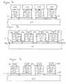
- FIGS. 4 a and 4 billustrate examples of plan views of patterns of metal traces 11 on first (primary) headers 107 ′ for respective thermoelectric devices according to embodiments of the present invention.
- 17 metal traces 111 a ′- 111 q ′ on the header 107 ′ for a single thermoelectric devicemay be configured to receive 32 different thermoelectric elements (16 p-type thermoelectric elements and 16 n-type thermoelectric elements) formed as discussed above with respect to FIGS. 2 a - 2 c .
- each of the interior traces 111 b ′- 111 p ′may receive one n-type thermoelectric element and one p-type thermoelectric element
- the terminal traces 111 a ′ and 111 q ′may each have a single thermoelectric element of opposite conductivity types (e.g., one n-type thermoelectric element on terminal trace 111 a ′ and one p-type thermoelectric element on terminal trace 111 q ′).
- 5 metal traces 111 a ′′- 111 e ′′ on the header 107 ′′ for a single thermoelectric devicemay be configured to receive 8 different thermoelectric elements (4 p-type thermoelectric elements and 4 n-type thermoelectric elements) formed as discussed above with respect to FIGS. 2 a - 2 c .
- each of the interior traces 111 b ′′- 111 d ′′may receive one n-type thermoelectric element and one p-type thermoelectric element
- the terminal traces 111 a ′′ and 111 e ′′may each have a single thermoelectric element of opposite conductivity types (e.g., one n-type thermoelectric element on terminal trace 111 a ′′ and one p-type thermoelectric element on terminal trace 111 e ′′).
- a single first (primary) header 107may include trace patterns for a plurality of different thermoelectric devices, so that the single first header 107 may provide a common substrate for batch assembly of multiple thermoelectric devices.
- a single headermay include a plurality of the traces patterns illustrated in FIG. 4 a for batch assembly of a plurality of thermoelectric devices with each device including 16 p-type thermoelectric elements and 16 n-type thermoelectric elements.
- a single headermay include a plurality of the traces patterns illustrated in FIG. 4 b for batch assembly of a plurality of thermoelectric devices with each device including 4 p-type thermoelectric elements and 4 n-type thermoelectric elements.
- FIGS. 5 a - 5 bare cross-sectional views illustrating steps of forming metal traces 115 on a second (secondary) header 109 according to embodiments of the present invention.
- the header 109may be a layer of a thermally conductive and electrically insulating material, such as aluminum nitride (AlN).
- AlNaluminum nitride
- portions of the header 109may be thermally conductive with a layer of insulating material thereon to provide electrical isolation between electrically conductive traces on the header.
- a continuous seed layer 114 amay be formed on the header 109 .
- the continuous seed layer 114 amay include an adhesion layer (such as a titanium layer) on the header 109 and a conduction layer (such as a copper layer) on the adhesion layer so that the adhesion layer is between the conduction layer and the header 109 .
- Metal traces 115may then be selectively formed on the continuous seed layer 114 a .
- a plating mask for the tracesmay be formed on the continuous seed layer 114 a , the metal traces 115 may be selectively plated on exposed portions of the continuous seed layer 114 a , and the plating mask for the traces may then be removed.
- the metal traces 115may include a conduction layer (such as a copper layer) on the continuous seed layer 114 a , a barrier layer (such as a nickel layer) on the conduction layer, and a passivation layer (such as a gold layer) on the barrier layer, so that the conduction layer is between the barrier layer and the continuous seed layer 114 a , and so that the conduction and barrier layers are between the passivation layer and the continuous seed layer 114 a .
- a conduction layersuch as a copper layer
- a barrier layersuch as a nickel layer
- a passivation layersuch as a gold layer
- the conduction layermay be a copper layer having a thickness of about 30 ⁇ m (micrometer)
- the barrier layermay be a nickel layer having a thickness of about 0.5 ⁇ m (micrometer)
- the passivation layermay be a gold layer having a thickness of about 0.5 ⁇ m (micrometer).
- Solder layers 135may then be selectively formed on the metal traces 115 .
- a plating mask for the solder layersmay be formed on the continuous seed layer 114 a and on the metal traces 115 , the solder layers 135 may be selectively plated on exposed portions of the metal traces 115 , and the plating mask for the solder layers may then be removed.
- Each solder layer 135may be a layer of a single element solder, a binary solder, a ternary solder, etc.
- the solder layers 135may include a solder material different than the solder material used for the solder layers 209 discussed above with respect to FIGS. 2 a - 2 c so that the solder layers 135 and 209 have different melting (reflow) temperatures.
- the solder layers 209may have a higher melting (reflow) temperature than the solder layers 135 so that thermoelectric elements may be soldered to the first header 107 at a first relatively high temperature using high temperature solder layers 209 , and then soldered to the second header 109 at a second relatively low temperature using low temperature solder layers 135 (without melting the high temperature solder layers 209 ).
- the solder layers 135may be layers of indium (In)
- the solder layers 209may be layers of tin (Sn).
- solder layers 135may be provided on the thermoelectric elements 201 for subsequent solder bonding of thermoelectric elements 201 to the metal traces 115 . Accordingly, the metal traces 115 may be free of solder prior to bonding the thermoelectric elements 201 thereto.
- the second (secondary) header 109may then be singulated (for example, by cutting) to provide separate headers for separate thermoelectric devices.
- FIGS. 6 a and 6 billustrate examples of plan views of patterns of metal traces 115 and solder layers 135 on individual second (secondary) headers 109 (after singulation) for respective thermoelectric devices according to embodiments of the present invention.
- the second header 109 ′ pattern of traces 115 ′ and solder layers 135 ′ of FIG. 6 acorresponds to the trace pattern of first header 107 ′ of FIG. 4 a for a thermoelectric device including 16 p-type thermoelectric elements and 16 n-type thermoelectric elements.
- 16 metal traces 115 ′ on the header 109 ′ for a single thermoelectric devicemay be configured to receive 32 different thermoelectric elements (16 p-type thermoelectric elements and 16 n-type thermoelectric elements formed as discussed above with respect to FIGS. 2 a - 2 c ) on respective solder layers 135 ′. More particularly, one n-type thermoelectric element and one p-type thermoelectric element may be soldered to each metal trace 115 ′.
- the second header 109 ′′ pattern of traces 115 ′′ and solder layers 135 ′′ of FIG. 6 bcorresponds to the trace pattern of first header 107 ′′ of FIG. 4 b for a thermoelectric device including 4 p-type thermoelectric elements and 4 n-type thermoelectric elements.
- 4 metal traces 115 ′′ on the header 109 ′′ for a single thermoelectric devicemay be configured to receive 8 different thermoelectric elements (4 p-type thermoelectric elements and 4 n-type thermoelectric elements formed as discussed above with respect to FIGS. 2 a - 2 c ) on respective solder layers 115 ′′. More particularly, one n-type thermoelectric element and one p-type thermoelectric element may be soldered to each metal trace 115 ′′.
- a single substrate/headermay include trace patterns for a plurality of different thermoelectric devices, so that metal traces and solder layers for a plurality of second headers 109 may be formed simultaneously on a same substrate/header. After forming the metal traces 115 and/or solder layers 135 , second headers 109 may be singulated from the common substrate before bonding with thermoelectric elements. A discussed above with respect to FIGS. 3 a - b and 4 a - b , a plurality of first headers 107 may be maintained on a common substrate to facilitate batch processing of a plurality of thermoelectric devices.
- thermoelectric elements 201 - p and 201 - nmay be removed from respective dicing films 211 and placed on traces 111 .
- thermoelectric elements 201 - p and 201 - nmay be placed, a reflow operation may be performed to provide an electrical and mechanical connection between the thermoelectric elements 201 - p and 201 - n and the metal traces 111 using solder layers 209 .
- the p-type thermoelectric elements 201 - pmay be formed from a p-type thermoelectric layer(s) on a growth substrate(s) as discussed above with respect to FIGS. 2 a - 2 c .
- the n-type thermoelectric elements 201 - nmay be formed from an n-type thermoelectric layer(s) on a growth substrate(s) as discussed above with respect to FIGS. 2 a - 2 c .
- a single dicing filmmay thus be populated with thermoelectric elements of only one conductivity type.
- solder layers 209may be formed on the respective thermoelectric elements before placement on the traces 111 .
- the solder layers 209may be formed on the metal traces 111 before placement of the thermoelectric elements 201 - p and 201 - n thereon.
- thermoelectric elements 201 - p and 201 - nmay be soldering the thermoelectric elements to the metal traces as shown in FIG. 7 a .
- the remaining portions 203 of the growth substrates and the buffer layers 205may be removed from the thermoelectric elements, for example using a chemical etch, thereby exposing growth surfaces of the thermoelectric elements.
- a conformal plating seed layer 701 amay be formed on the first header 107 , on the metal traces 111 , on the exposed surfaces of the thermoelectric elements 201 - p and 201 - n , and on exposed sidewalls.
- the plating seed layer 701 amay include an adhesion layer (such as a titanium layer) on the thermoelectric elements and a conduction layer (such as a copper layer) on the adhesion layer so that the adhesion layer is between the conduction layer and the thermoelectric elements.
- the plating seed layer 701 amay include an adhesion layer (such as a chromium layer) on the thermoelectric elements, a barrier layer (such as a nickel layer) on the adhesion layer, and passivation layer (such as a gold layer) on the barrier layer, so that the adhesion layer is between the barrier layer and the thermoelectric elements, and so that the adhesion and barrier layers are between the passivation layer and the thermoelectric elements.
- the plating seed layer 701 amay be formed by sputtering and/or evaporation.
- a plating mask 703(such as a photoresist mask) may be formed on the plating seed layer 701 a , and the plating mask 703 may selectively expose portions of the plating seed layer 701 a on the thermoelectric elements 201 - p and 201 - n .
- Metal posts 133may then be plated on exposed portions of the plating seed layer 701 a using the plating seed layer 701 a as an electroplating electrode.
- Each metal post 133may include a conduction layer (such as a copper layer) on the plating seed layer 701 a , a barrier layer (such as a nickel layer) on the conduction layer, and a passivation layer (such as a gold layer) on the barrier layer, so that the conduction layer is between the barrier layer and the plating seed layer 701 a , and so that the conduction and barrier layers are between the passivation layer and the plating seed layer 701 a .
- a conduction layersuch as a copper layer
- a barrier layersuch as a nickel layer
- a passivation layersuch as a gold layer
- the conduction layermay be a copper layer having a thickness of about 30 ⁇ m (micrometer)
- the barrier layermay be a nickel layer having a thickness of about 0.5 ⁇ m (micrometer)
- the passivation layermay be a gold layer having a thickness of about 0.5 ⁇ m (micrometer).
- Each post 133may thus have a thickness of at least about 15 ⁇ m (micrometer) in a direction between the thermoelectric element and the second header 109 .
- each post 133may have a thickness in the range of about 20 ⁇ m (micrometer) to about 40 ⁇ m (micrometer), and more particularly a thickness of about 30 ⁇ m (micrometer), in a direction between the thermoelectric element and the second header 109 .
- the plating mask 703may be removed, and exposed portions of the plating seed layer 701 a may be removed as shown in FIG. 7 c .
- solder layers 135 of the second header of FIG. 5 bmay then be brought into contact with the with the respective metal posts 133 , and a reflow operation may be performed to provide electrical and mechanical connection between the thermoelectric elements 201 - p and 201 - n and the metal traces 115 using solder layers 135 .
- the solder layers 135may be provided on the metal traces 115 before contacting the metal posts 133 .
- solder layers 135may be formed on the metal posts 133 before contacting the traces 115 of the second header (so that the second header 109 of FIG. 5 b may be free of solder layers 135 ).
- the plating mask 703 and the plating seed layer 701 a of FIG. 7 bmay be used to plate the solder layers 135 on the metal posts 133 .
- FIGS. 8 a - 8 care plan views illustrating the final assembly of a first header as shown in FIG. 4 b and a second header as illustrated in FIG. 6 b to provide a thermoelectric device according to embodiments of the present invention. More particularly, FIG. 8 a corresponds to the cross-sectional view of FIG. 7 c , and FIG. 8 b corresponds to the cross-sectional view of FIG. 7 d . FIG. 8 c illustrates singulation of the first header to provide a plurality of thermoelectric devices.
- patterns of metal traces 111 for a plurality of thermoelectric devicesmay be formed on a common header 107 (also referred to as a substrate) to facilitate batch assembly operations.
- a common header 107also referred to as a substrate
- the n-type thermoelectric elements 201 - n and the p-type thermoelectric elements 201 - pmay be soldered to the traces 111 , and the metal posts 133 may be formed on the thermoelectric elements.
- the second headers 109may be previously formed with metal traces and solder thereon and singulated as discussed above with respect to FIG. 4 b , and a separate second header 109 may be bonded face down on respective patterns of traces 111 and thermoelectric elements 201 - n and 201 - p as shown in FIGS. 7 d and 8 b . Accordingly, the backsides 109 a of the second headers 109 are visible in the plan view of FIG. 8 b with the thermoelectric elements 201 - p and 201 - n being sandwiched between the first header 107 and the respective second headers 109 .
- the first header 107may then be singulated into a plurality of first headers 107 s as shown in FIG. 8 c to provide a plurality of separate thermoelectric devices.
- portions of the terminal traces 111 a and 111 emay be exposed to provide electrical coupling to external circuitry such as a controller for a thermoelectric cooling device and/or an electrical storage device and/or load for a thermoelectric power generation device.
- external circuitrysuch as a controller for a thermoelectric cooling device and/or an electrical storage device and/or load for a thermoelectric power generation device.
- a thermoelectric cooling deviceone of the headers 107 s or 109 may be thermally coupled to a surface to be cooled, and the other header may be thermally coupled to a heat sink.
- one of the headersmay be coupled to a relatively hot surface and the other of the headers may be coupled to a relatively cool surface.
- thermoelectric devices having header patternsas shown in FIGS. 4 b and 6 b
- same fabrication stepscan be used to fabricate thermoelectric devices having other header patterns such as the patterns illustrated in FIGS. 4 a and 6 a.
Landscapes
- Engineering & Computer Science (AREA)
- Manufacturing & Machinery (AREA)
- Cooling Or The Like Of Semiconductors Or Solid State Devices (AREA)
Abstract
Description
ZT=(α2T/σKT), (equation 1)
where α, T, σ, KTare the Seebeck coefficient, absolute temperature, electrical conductivity, and total thermal conductivity, respectively. The material-coefficient Z can be expressed in terms of lattice thermal conductivity (KL), electronic thermal conductivity (Ke) and carrier mobility (i), for a given carrier density (μ) and the corresponding α, yielding equation (2) below:
Z=α2σ/(KL+Ke)=α2/[KL/(μρq)+L0T)], (equation 2)
where, L0is the Lorenz number (approximately 1.5×10⁻⁸V2/K2in non-degenerate semiconductors). State-of-the-art thermoelectric devices may use alloys, such as p-BixSb2-xTe3-ySey(x≈0.5, y≈0.12) and n-Bi2(SeyTe1-y)3(y≈0.05) for the 200 degree K to 400 degree K temperature range. For certain alloys, KLmay be reduced more strongly than μ leading to enhanced ZT.
Claims (7)
Priority Applications (1)
| Application Number | Priority Date | Filing Date | Title |
|---|---|---|---|
| US11/472,032US8623687B2 (en) | 2005-06-22 | 2006-06-21 | Methods of forming thermoelectric devices including conductive posts and/or different solder materials and related methods and structures |
Applications Claiming Priority (2)
| Application Number | Priority Date | Filing Date | Title |
|---|---|---|---|
| US69286405P | 2005-06-22 | 2005-06-22 | |
| US11/472,032US8623687B2 (en) | 2005-06-22 | 2006-06-21 | Methods of forming thermoelectric devices including conductive posts and/or different solder materials and related methods and structures |
Publications (2)
| Publication Number | Publication Date |
|---|---|
| US20060289052A1 US20060289052A1 (en) | 2006-12-28 |
| US8623687B2true US8623687B2 (en) | 2014-01-07 |
Family
ID=37101689
Family Applications (1)
| Application Number | Title | Priority Date | Filing Date |
|---|---|---|---|
| US11/472,032Active2031-01-28US8623687B2 (en) | 2005-06-22 | 2006-06-21 | Methods of forming thermoelectric devices including conductive posts and/or different solder materials and related methods and structures |
Country Status (2)
| Country | Link |
|---|---|
| US (1) | US8623687B2 (en) |
| WO (1) | WO2007002337A2 (en) |
Cited By (1)
| Publication number | Priority date | Publication date | Assignee | Title |
|---|---|---|---|---|
| US20170211854A1 (en)* | 2014-05-23 | 2017-07-27 | Laird Durham, Inc. | Thermoelectric heating/cooling devices including resistive heaters |
Families Citing this family (35)
| Publication number | Priority date | Publication date | Assignee | Title |
|---|---|---|---|---|
| JP2006507690A (en)* | 2002-11-25 | 2006-03-02 | ネクストリーム・サーマル・ソリューションズ | Transformer thermoelectric device |
| US7679203B2 (en) | 2006-03-03 | 2010-03-16 | Nextreme Thermal Solutions, Inc. | Methods of forming thermoelectric devices using islands of thermoelectric material and related structures |
| US7768040B2 (en)* | 2006-10-23 | 2010-08-03 | Micron Technology, Inc. | Imager device with electric connections to electrical device |
| US20080178920A1 (en)* | 2006-12-28 | 2008-07-31 | Schlumberger Technology Corporation | Devices for cooling and power |
| US20080264464A1 (en)* | 2007-01-11 | 2008-10-30 | Nextreme Thermal Solutions, Inc. | Temperature Control Including Integrated Thermoelectric Sensing and Heat Pumping Devices and Related Methods and Systems |
| US8267984B2 (en)* | 2007-08-03 | 2012-09-18 | Scion Neurostim, Llc. | Neurophysiological activation by vestibular or cranial nerve stimulation |
| US20080168775A1 (en)* | 2007-01-11 | 2008-07-17 | Nextreme Thermal Solutions, Inc. | Temperature Control Including Integrated Thermoelectric Temperature Sensing and Related Methods and Systems |
| US8696724B2 (en)* | 2007-01-11 | 2014-04-15 | Scion Neurostim, Llc. | Devices for vestibular or cranial nerve stimulation |
| US8267983B2 (en)* | 2007-01-11 | 2012-09-18 | Scion Neurostim, Llc. | Medical devices incorporating thermoelectric transducer and controller |
| US20090000652A1 (en)* | 2007-06-26 | 2009-01-01 | Nextreme Thermal Solutions, Inc. | Thermoelectric Structures Including Bridging Thermoelectric Elements |
| US7855397B2 (en)* | 2007-09-14 | 2010-12-21 | Nextreme Thermal Solutions, Inc. | Electronic assemblies providing active side heat pumping |
| DE102008005694B4 (en)* | 2008-01-23 | 2015-05-07 | Fraunhofer-Gesellschaft zur Förderung der angewandten Forschung e.V. | Method for producing a thermoelectric component |
| US20090199887A1 (en)* | 2008-02-08 | 2009-08-13 | North Carolina State University And Nextreme Thermal Solutions, Inc. | Methods of forming thermoelectric devices including epitaxial thermoelectric elements of different conductivity types on a same substrate and related structures |
| US20090205696A1 (en)* | 2008-02-15 | 2009-08-20 | Nextreme Thermal Solutions, Inc. | Thermoelectric Heat Pumps Providing Active Thermal Barriers and Related Devices and Methods |
| US20110000224A1 (en)* | 2008-03-19 | 2011-01-06 | Uttam Ghoshal | Metal-core thermoelectric cooling and power generation device |
| US8525016B2 (en) | 2009-04-02 | 2013-09-03 | Nextreme Thermal Solutions, Inc. | Thermoelectric devices including thermoelectric elements having off-set metal pads and related structures, methods, and systems |
| IN2012DN01366A (en) | 2009-07-17 | 2015-06-05 | Sheetak Inc | |
| WO2011075574A1 (en) | 2009-12-18 | 2011-06-23 | Scion Neurostim, Llc | Devices and methods for vestibular and/or cranial nerve stimulation |
| US9601677B2 (en)* | 2010-03-15 | 2017-03-21 | Laird Durham, Inc. | Thermoelectric (TE) devices/structures including thermoelectric elements with exposed major surfaces |
| US8498127B2 (en)* | 2010-09-10 | 2013-07-30 | Ge Intelligent Platforms, Inc. | Thermal interface material for reducing thermal resistance and method of making the same |
| JP6580298B2 (en) | 2010-12-16 | 2019-09-25 | サイオン・ニューロスティム,リミテッド・ライアビリティ・カンパニー | Vestibular stimulation device and vestibular stimulation system |
| US10537467B2 (en) | 2010-12-16 | 2020-01-21 | Scion Neurostim, Llc | Systems, devices and methods for bilateral caloric vestibular stimulation |
| US10512564B2 (en) | 2010-12-16 | 2019-12-24 | Scion Neurostim, Llc | Combination treatments |
| US9744074B2 (en) | 2010-12-16 | 2017-08-29 | Scion Neurostim, Llc | Combination treatments |
| US9981137B2 (en)* | 2012-01-27 | 2018-05-29 | Nuvectra Corporation | Heat dispersion for implantable medical devices |
| FR2994336B1 (en)* | 2012-08-02 | 2016-10-21 | Valeo Systemes Thermiques | PROCESS FOR MANUFACTURING A THERMO ELECTRIC MODULE, IN PARTICULAR FOR GENERATING AN ELECTRICAL CURRENT IN A MOTOR VEHICLE, AND THERMO ELECTRIC MODULE OBTAINED BY SAID METHOD. |
| KR20140083357A (en)* | 2012-12-26 | 2014-07-04 | 서울바이오시스 주식회사 | Method for separating substrate and methos for fabricating semiconductor device using the same |
| US20140332048A1 (en)* | 2013-05-08 | 2014-11-13 | Vern Green Power Solutions, Llc | Thermoelectric device |
| WO2016134285A1 (en)* | 2015-02-19 | 2016-08-25 | Novus Energy Technologies, Inc. | Large footprint, high power density thermoelectric modules for high temperature applications |
| US11658095B2 (en)* | 2019-03-29 | 2023-05-23 | Intel Corporation | Bump integrated thermoelectric cooler |
| CN113130731A (en)* | 2019-12-30 | 2021-07-16 | 华为技术有限公司 | Thermoelectric refrigerator, method for manufacturing thermoelectric refrigerator, and electronic apparatus |
| US12382830B2 (en)* | 2021-06-23 | 2025-08-05 | The Johns Hopkins University | Large area scalable fabrication methodologies for versatile thermoelectric device modules |
| CN114293162A (en)* | 2021-12-15 | 2022-04-08 | 先导薄膜材料(广东)有限公司 | Method for effectively removing thin film oxide layer for TEC and application |
| CN114457316A (en)* | 2022-01-24 | 2022-05-10 | 先导薄膜材料(广东)有限公司 | A kind of preparation method of composite film for thermoelectric material welding |
| US20230403935A1 (en)* | 2022-05-20 | 2023-12-14 | Apple Inc. | Thermoelectric Cooling Modules |
Citations (58)
| Publication number | Priority date | Publication date | Assignee | Title |
|---|---|---|---|---|
| US3136134A (en) | 1960-11-16 | 1964-06-09 | Bell Telephone Labor Inc | Thermoelectric refrigerator |
| US3296034A (en) | 1962-01-04 | 1967-01-03 | Borg Warner | Thermoelectric assembly and method of fabrication |
| US3607444A (en) | 1966-12-06 | 1971-09-21 | Siemens Ag | Thermoelectric assembly |
| US3663307A (en) | 1968-02-14 | 1972-05-16 | Westinghouse Electric Corp | Thermoelectric device |
| US3859143A (en) | 1970-07-23 | 1975-01-07 | Rca Corp | Stable bonded barrier layer-telluride thermoelectric device |
| US4443650A (en)* | 1981-04-17 | 1984-04-17 | Kyoto University | Thermoelectric converter element |
| US4459428A (en)* | 1982-04-28 | 1984-07-10 | Energy Conversion Devices, Inc. | Thermoelectric device and method of making same |
| US4468854A (en)* | 1982-04-29 | 1984-09-04 | Ecd-Anr Energy Conversion Company | Method and apparatus for manufacturing thermoelectric devices |
| GB2171254A (en) | 1985-02-19 | 1986-08-20 | Energy Conversion Devices Inc | Thermoelectric element thermoelectric device and methods of manufacturing the same |
| US4855810A (en) | 1987-06-02 | 1989-08-08 | Gelb Allan S | Thermoelectric heat pump |
| US5006178A (en) | 1988-04-27 | 1991-04-09 | Theodorus Bijvoets | Thermo-electric device with each element containing two halves and an intermediate connector piece of differing conductivity |
| US5254178A (en) | 1990-10-30 | 1993-10-19 | Nippondenso Co., Ltd. | Thermoelectric transducer apparatus comprising N- and P-type semiconductors and having electronic control capabilities |
| JPH0697512A (en) | 1992-09-16 | 1994-04-08 | Sumitomo Special Metals Co Ltd | Thermoelectric conversion element |
| US5429680A (en)* | 1993-11-19 | 1995-07-04 | Fuschetti; Dean F. | Thermoelectric heat pump |
| US5430322A (en) | 1992-09-08 | 1995-07-04 | Agency Of Industrial Science And Technology | Thermoelectric element sheet in which thermoelectric semiconductors are mounted between films |
| EP0687020A1 (en) | 1994-05-23 | 1995-12-13 | Seiko Instruments Inc. | Thermoelectric device and a method of manufacturing thereof |
| EP0805501A1 (en) | 1995-09-29 | 1997-11-05 | Union Material Inc. | Thermoelectric device and thermoelectric cooler/heater |
| WO1998043740A2 (en) | 1997-03-28 | 1998-10-08 | The Perkin-Elmer Corporation | Improvements in thermal cycler for pcr |
| WO1998044562A1 (en) | 1997-03-31 | 1998-10-08 | Research Triangle Institute | Thin-film thermoelectric device and fabrication method of same |
| US5837929A (en) | 1994-07-05 | 1998-11-17 | Mantron, Inc. | Microelectronic thermoelectric device and systems incorporating such device |
| US5865975A (en) | 1995-06-06 | 1999-02-02 | Academy Of Applied Science | Automatic protein and/or DNA analysis system and method |
| US5869242A (en) | 1995-09-18 | 1999-02-09 | Myriad Genetics, Inc. | Mass spectrometry to assess DNA sequence polymorphisms |
| US5874219A (en) | 1995-06-07 | 1999-02-23 | Affymetrix, Inc. | Methods for concurrently processing multiple biological chip assays |
| US5900071A (en) | 1993-01-12 | 1999-05-04 | Massachusetts Institute Of Technology | Superlattice structures particularly suitable for use as thermoelectric materials |
| US5922988A (en) | 1996-07-16 | 1999-07-13 | Honda Giken Kogyo Kabushiki Kaisha | Thermoelectric material |
| WO1999038219A1 (en) | 1998-01-26 | 1999-07-29 | California Institute Of Technology | Electronic device featuring thermoelectric power generation |
| US6060331A (en) | 1996-12-17 | 2000-05-09 | The Regents Of The University Of California | Method for making heterostructure thermionic coolers |
| US6060657A (en) | 1998-06-24 | 2000-05-09 | Massachusetts Institute Of Technology | Lead-chalcogenide superlattice structures |
| US6062681A (en) | 1998-07-14 | 2000-05-16 | Hewlett-Packard Company | Bubble valve and bubble valve-based pressure regulator |
| US6071351A (en) | 1996-05-02 | 2000-06-06 | Research Triangle Institute | Low temperature chemical vapor deposition and etching apparatus and method |
| US6072925A (en) | 1991-12-05 | 2000-06-06 | Canon Kabushiki Kaisha | Optical integrated nodes, and optical communication systems and networks using the optical integrated nodes |
| US6075280A (en)* | 1997-12-31 | 2000-06-13 | Winbond Electronics Corporation | Precision breaking of semiconductor wafer into chips by applying an etch process |
| US6084050A (en) | 1997-01-09 | 2000-07-04 | Nippon Telegraph And Telephone Corporation | Thermo-optic devices |
| US6094919A (en) | 1999-01-04 | 2000-08-01 | Intel Corporation | Package with integrated thermoelectric module for cooling of integrated circuits |
| US6100463A (en)* | 1997-11-18 | 2000-08-08 | The Boeing Company | Method for making advanced thermoelectric devices |
| WO2000049664A1 (en) | 1999-02-19 | 2000-08-24 | Peltech S.R.L. | Solid state thermoelectric device |
| US6154266A (en) | 1997-03-31 | 2000-11-28 | Nec Corporation | Method of manufacturing liquid crystal display device |
| US6154479A (en) | 1994-10-13 | 2000-11-28 | Nec Corporation | VCSELs (vertical-cavity surface emitting lasers) and VCSEL-based devices |
| US6180351B1 (en) | 1999-07-22 | 2001-01-30 | Agilent Technologies Inc. | Chemical array fabrication with identifier |
| WO2001008800A1 (en) | 1999-07-30 | 2001-02-08 | Bio-Rad Laboratories, Inc. | Temperature control for multi-vessel reaction apparatus |
| US6271459B1 (en) | 2000-04-26 | 2001-08-07 | Wafermasters, Inc. | Heat management in wafer processing equipment using thermoelectric device |
| US6282907B1 (en) | 1999-12-09 | 2001-09-04 | International Business Machines Corporation | Thermoelectric cooling apparatus and method for maximizing energy transport |
| US20010052234A1 (en) | 2000-03-21 | 2001-12-20 | Research Triangle Institute | Cascade cryogenic thermoelectric cooler for cryogenic and room temperature applications |
| US6365821B1 (en) | 2000-07-24 | 2002-04-02 | Intel Corporation | Thermoelectrically cooling electronic devices |
| US6384312B1 (en) | 2000-12-07 | 2002-05-07 | International Business Machines Corporation | Thermoelectric coolers with enhanced structured interfaces |
| US20020053359A1 (en) | 1999-08-27 | 2002-05-09 | Harman Theodore C. | Nanostructured thermoelectric materials and devices |
| US6388185B1 (en)* | 1998-08-07 | 2002-05-14 | California Institute Of Technology | Microfabricated thermoelectric power-generation devices |
| US6403876B1 (en) | 2000-12-07 | 2002-06-11 | International Business Machines Corporation | Enhanced interface thermoelectric coolers with all-metal tips |
| US20020069906A1 (en) | 2000-03-24 | 2002-06-13 | Chris Macris | Thermoelectric device and method of manufacture |
| US6410971B1 (en) | 2001-07-12 | 2002-06-25 | Ferrotec (Usa) Corporation | Thermoelectric module with thin film substrates |
| US6412286B1 (en) | 2001-04-24 | 2002-07-02 | Samsung Electronics Co., Ltd. | Storage box using a thermoelement and a cooling method for a storage box |
| US6452206B1 (en)* | 1997-03-17 | 2002-09-17 | Massachusetts Institute Of Technology | Superlattice structures for use in thermoelectric devices |
| US20020139123A1 (en) | 2001-02-09 | 2002-10-03 | Bell Lon E. | Efficiency thermoelectrics utilizing thermal isolation |
| US20030230332A1 (en)* | 2002-04-15 | 2003-12-18 | Research Triangle Institute | Thermoelectric device utilizing double-sided peltier junctions and method of making the device |
| US20040261830A1 (en)* | 2001-06-01 | 2004-12-30 | Marlow Industries, Inc. | Thermoelectric device having P-type and N-type materials |
| US20050045702A1 (en)* | 2003-08-29 | 2005-03-03 | William Freeman | Thermoelectric modules and methods of manufacture |
| US20050178424A1 (en)* | 2003-11-17 | 2005-08-18 | Matsushita Electric Industrial Co., Ltd. | Method of manufacturing crystalline film, method of manufacturing crystalline-film-layered substrate, method of manufacturing thermoelectric conversion element, and thermoelectric conversion element |
| WO2006049285A2 (en) | 2004-11-02 | 2006-05-11 | Showa Denko K.K. | Thermoelectric conversion module, thermoelectric power generating apparatus and method using same |
- 2006
- 2006-06-21WOPCT/US2006/024387patent/WO2007002337A2/enactiveApplication Filing
- 2006-06-21USUS11/472,032patent/US8623687B2/enactiveActive
Patent Citations (64)
| Publication number | Priority date | Publication date | Assignee | Title |
|---|---|---|---|---|
| US3136134A (en) | 1960-11-16 | 1964-06-09 | Bell Telephone Labor Inc | Thermoelectric refrigerator |
| US3296034A (en) | 1962-01-04 | 1967-01-03 | Borg Warner | Thermoelectric assembly and method of fabrication |
| US3607444A (en) | 1966-12-06 | 1971-09-21 | Siemens Ag | Thermoelectric assembly |
| US3663307A (en) | 1968-02-14 | 1972-05-16 | Westinghouse Electric Corp | Thermoelectric device |
| US3859143A (en) | 1970-07-23 | 1975-01-07 | Rca Corp | Stable bonded barrier layer-telluride thermoelectric device |
| US4443650A (en)* | 1981-04-17 | 1984-04-17 | Kyoto University | Thermoelectric converter element |
| US4459428A (en)* | 1982-04-28 | 1984-07-10 | Energy Conversion Devices, Inc. | Thermoelectric device and method of making same |
| US4468854A (en)* | 1982-04-29 | 1984-09-04 | Ecd-Anr Energy Conversion Company | Method and apparatus for manufacturing thermoelectric devices |
| GB2171254A (en) | 1985-02-19 | 1986-08-20 | Energy Conversion Devices Inc | Thermoelectric element thermoelectric device and methods of manufacturing the same |
| US4855810A (en) | 1987-06-02 | 1989-08-08 | Gelb Allan S | Thermoelectric heat pump |
| US5006178A (en) | 1988-04-27 | 1991-04-09 | Theodorus Bijvoets | Thermo-electric device with each element containing two halves and an intermediate connector piece of differing conductivity |
| US5254178A (en) | 1990-10-30 | 1993-10-19 | Nippondenso Co., Ltd. | Thermoelectric transducer apparatus comprising N- and P-type semiconductors and having electronic control capabilities |
| US6072925A (en) | 1991-12-05 | 2000-06-06 | Canon Kabushiki Kaisha | Optical integrated nodes, and optical communication systems and networks using the optical integrated nodes |
| US5430322A (en) | 1992-09-08 | 1995-07-04 | Agency Of Industrial Science And Technology | Thermoelectric element sheet in which thermoelectric semiconductors are mounted between films |
| JPH0697512A (en) | 1992-09-16 | 1994-04-08 | Sumitomo Special Metals Co Ltd | Thermoelectric conversion element |
| US5900071A (en) | 1993-01-12 | 1999-05-04 | Massachusetts Institute Of Technology | Superlattice structures particularly suitable for use as thermoelectric materials |
| US5429680A (en)* | 1993-11-19 | 1995-07-04 | Fuschetti; Dean F. | Thermoelectric heat pump |
| EP0687020A1 (en) | 1994-05-23 | 1995-12-13 | Seiko Instruments Inc. | Thermoelectric device and a method of manufacturing thereof |
| US5824561A (en)* | 1994-05-23 | 1998-10-20 | Seiko Instruments Inc. | Thermoelectric device and a method of manufacturing thereof |
| US5837929A (en) | 1994-07-05 | 1998-11-17 | Mantron, Inc. | Microelectronic thermoelectric device and systems incorporating such device |
| US6154479A (en) | 1994-10-13 | 2000-11-28 | Nec Corporation | VCSELs (vertical-cavity surface emitting lasers) and VCSEL-based devices |
| US5865975A (en) | 1995-06-06 | 1999-02-02 | Academy Of Applied Science | Automatic protein and/or DNA analysis system and method |
| US5874219A (en) | 1995-06-07 | 1999-02-23 | Affymetrix, Inc. | Methods for concurrently processing multiple biological chip assays |
| US5869242A (en) | 1995-09-18 | 1999-02-09 | Myriad Genetics, Inc. | Mass spectrometry to assess DNA sequence polymorphisms |
| EP0805501A1 (en) | 1995-09-29 | 1997-11-05 | Union Material Inc. | Thermoelectric device and thermoelectric cooler/heater |
| US6071351A (en) | 1996-05-02 | 2000-06-06 | Research Triangle Institute | Low temperature chemical vapor deposition and etching apparatus and method |
| US5922988A (en) | 1996-07-16 | 1999-07-13 | Honda Giken Kogyo Kabushiki Kaisha | Thermoelectric material |
| US6060331A (en) | 1996-12-17 | 2000-05-09 | The Regents Of The University Of California | Method for making heterostructure thermionic coolers |
| US6084050A (en) | 1997-01-09 | 2000-07-04 | Nippon Telegraph And Telephone Corporation | Thermo-optic devices |
| US6452206B1 (en)* | 1997-03-17 | 2002-09-17 | Massachusetts Institute Of Technology | Superlattice structures for use in thermoelectric devices |
| WO1998043740A2 (en) | 1997-03-28 | 1998-10-08 | The Perkin-Elmer Corporation | Improvements in thermal cycler for pcr |
| US6154266A (en) | 1997-03-31 | 2000-11-28 | Nec Corporation | Method of manufacturing liquid crystal display device |
| US6300150B1 (en)* | 1997-03-31 | 2001-10-09 | Research Triangle Institute | Thin-film thermoelectric device and fabrication method of same |
| WO1998044562A1 (en) | 1997-03-31 | 1998-10-08 | Research Triangle Institute | Thin-film thermoelectric device and fabrication method of same |
| US6100463A (en)* | 1997-11-18 | 2000-08-08 | The Boeing Company | Method for making advanced thermoelectric devices |
| US6075280A (en)* | 1997-12-31 | 2000-06-13 | Winbond Electronics Corporation | Precision breaking of semiconductor wafer into chips by applying an etch process |
| WO1999038219A1 (en) | 1998-01-26 | 1999-07-29 | California Institute Of Technology | Electronic device featuring thermoelectric power generation |
| US6060657A (en) | 1998-06-24 | 2000-05-09 | Massachusetts Institute Of Technology | Lead-chalcogenide superlattice structures |
| US6062681A (en) | 1998-07-14 | 2000-05-16 | Hewlett-Packard Company | Bubble valve and bubble valve-based pressure regulator |
| US6388185B1 (en)* | 1998-08-07 | 2002-05-14 | California Institute Of Technology | Microfabricated thermoelectric power-generation devices |
| US6094919A (en) | 1999-01-04 | 2000-08-01 | Intel Corporation | Package with integrated thermoelectric module for cooling of integrated circuits |
| WO2000049664A1 (en) | 1999-02-19 | 2000-08-24 | Peltech S.R.L. | Solid state thermoelectric device |
| US6180351B1 (en) | 1999-07-22 | 2001-01-30 | Agilent Technologies Inc. | Chemical array fabrication with identifier |
| WO2001008800A1 (en) | 1999-07-30 | 2001-02-08 | Bio-Rad Laboratories, Inc. | Temperature control for multi-vessel reaction apparatus |
| US20020053359A1 (en) | 1999-08-27 | 2002-05-09 | Harman Theodore C. | Nanostructured thermoelectric materials and devices |
| US6605772B2 (en) | 1999-08-27 | 2003-08-12 | Massachusetts Institute Of Technology | Nanostructured thermoelectric materials and devices |
| US6282907B1 (en) | 1999-12-09 | 2001-09-04 | International Business Machines Corporation | Thermoelectric cooling apparatus and method for maximizing energy transport |
| US6505468B2 (en) | 2000-03-21 | 2003-01-14 | Research Triangle Institute | Cascade cryogenic thermoelectric cooler for cryogenic and room temperature applications |
| US20010052234A1 (en) | 2000-03-21 | 2001-12-20 | Research Triangle Institute | Cascade cryogenic thermoelectric cooler for cryogenic and room temperature applications |
| US20020069906A1 (en) | 2000-03-24 | 2002-06-13 | Chris Macris | Thermoelectric device and method of manufacture |
| US6271459B1 (en) | 2000-04-26 | 2001-08-07 | Wafermasters, Inc. | Heat management in wafer processing equipment using thermoelectric device |
| US6365821B1 (en) | 2000-07-24 | 2002-04-02 | Intel Corporation | Thermoelectrically cooling electronic devices |
| US6696635B2 (en) | 2000-07-24 | 2004-02-24 | Intel Corporation | Thermoelectrically cooling electronic devices |
| US6384312B1 (en) | 2000-12-07 | 2002-05-07 | International Business Machines Corporation | Thermoelectric coolers with enhanced structured interfaces |
| US6403876B1 (en) | 2000-12-07 | 2002-06-11 | International Business Machines Corporation | Enhanced interface thermoelectric coolers with all-metal tips |
| US20020139123A1 (en) | 2001-02-09 | 2002-10-03 | Bell Lon E. | Efficiency thermoelectrics utilizing thermal isolation |
| US6412286B1 (en) | 2001-04-24 | 2002-07-02 | Samsung Electronics Co., Ltd. | Storage box using a thermoelement and a cooling method for a storage box |
| US20040261830A1 (en)* | 2001-06-01 | 2004-12-30 | Marlow Industries, Inc. | Thermoelectric device having P-type and N-type materials |
| US6410971B1 (en) | 2001-07-12 | 2002-06-25 | Ferrotec (Usa) Corporation | Thermoelectric module with thin film substrates |
| US20030230332A1 (en)* | 2002-04-15 | 2003-12-18 | Research Triangle Institute | Thermoelectric device utilizing double-sided peltier junctions and method of making the device |
| US20050045702A1 (en)* | 2003-08-29 | 2005-03-03 | William Freeman | Thermoelectric modules and methods of manufacture |
| US20050178424A1 (en)* | 2003-11-17 | 2005-08-18 | Matsushita Electric Industrial Co., Ltd. | Method of manufacturing crystalline film, method of manufacturing crystalline-film-layered substrate, method of manufacturing thermoelectric conversion element, and thermoelectric conversion element |
| WO2006049285A2 (en) | 2004-11-02 | 2006-05-11 | Showa Denko K.K. | Thermoelectric conversion module, thermoelectric power generating apparatus and method using same |
| WO2006049285A3 (en) | 2004-11-02 | 2007-02-15 | Showa Denko Kk | Thermoelectric conversion module, thermoelectric power generating apparatus and method using same |
Non-Patent Citations (85)
| Title |
|---|
| 1.3 Peltier Cooling and the Thermoelectric Figure of Merit; G.S. Nolas et al.; Thermo-electrics Basic Principles and New Materials Developments; Materials Science; pp. 8-13. |
| 15.8%-Efficient (1-SUN, AM 1.5G) GaAs Solar Cell on Optical-Grade Polycrystalline Ge Substrate, Rama Venkatasubramanian et al., pp. 691-695, (1993). |
| 18.2% (AM1.5) Efficient GaAs Solar Cell on Optical-Grade Polycrystalline Ge Substrate, Rama Venkatasubramanian et al., 25th PVSC; May 13-17, 1996; Washington, D.C. 1996 IEEE pp. 31-36. |
| 20% (AM1.5) Efficiency GaAs Solar Cells on Sub-mm Grain-Size Poly-Ge and Its Transition to Low-Cost Substrates, Rama Venkatasubramanian et al., 26th PVSC: Sep. 30-Oct. 3, 1997; Anaheim, CA 1997 IEEE, pp. 811-814. |
| A Silent Cool: Thermoelectrics May Offer New Ways to Refrigerate and Generate Power, Corinna Wu, Science News, Sep. 6, 1997 v152 n10 p. 152(2), pp. 1-3. |
| Advances in the Development of an AIGaAs/GaAs Cascade Solar Cell Using a Patterned Germanium Tunnel Interconnect, Rama Venkatasubramanian et al., pp. 345-354, (1991). |
| An Inverted-Growth Approach to Development of an IR-Transparent, High-Efficiency AiGaAs/GaAs Cascade Solar Cell, Rama Venkatasubramanian, M.L. Timmons, T.S. Colpitts, J.S. Hills, and J.A. Hutchby, Research Triangle Institute, Research Triangle Park, NC 27709, 1991 IEEE pp. 93-98. |
| Close-Packed Cell Arrays for Dish Concentrators, J.B. Lasich et al., Solar Research Corporation Pty. Ltd., 6 Luton Lane, Hawthorn, Victoria 3122, Australia and M. Timmons et al., Research Triangle Institute, RTP, USA, 1994 IEEE pp. 1938-1941. |
| Compensation Mechanisms in N+-GaAs Doped With Silicon, Rama Venkatasubramanian, et al., Electrical Computer, and Systems Engineering Department, Rensselaer Polytechnic Institute, Troy, New York 12180, USA, Journal of Crystal Growth 94 (1989) pp. 34-40. |
| Cool New Film, Science Update, Oct. 11, 2001, http://www.nature.com/nsu/011011/0111011-12.html, pp. 1-2. |
| Cooling Film Tempers Tiny Hot Spots, Rama Venkatasubramanian et al, Science News, No. 3, 2001, V160, i18, p. 280. |
| CVD Diamond for Components and Emitters, J. Davidson, Corresponding Author, e-mail address: jld@vuse.vanderbilt.edu (J. Davidson) et al., Vanderbilt University 2201 West End Avenue, Nashville, TN 37235, USA, Diamond and Related Materials 10 (2001) pp. 1736-1742. |
| Development of 20% Efficient GainAsP Solar Cells, P.R. Sharps, et. al., 1993 IEEE pp. 633-638. |
| Development of High-Efficiency A10.2Ga0.8As Solar Cells and Interconnect Schemes For AI0.2Ga0.3As/Si Mechanically-Stacked Cascade Cells, Rama Venkatasubramanian, et al., 1993 IEEE pp. 752-756. |
| Development of Low-Bandgap Ge and SI0.07Ge0.03 Solar Cells for Monolithic and Mechanically-Stacked Cascade Applications, Rama Venkatasubramanian et al., pp. 73-78, (1990). |
| Electronic and Mechanical Properties of Ge Films Grown on Glass Substrates, R.K. Ahrenkiel et al., 26th PVSC; Sep. 30-Oct. 3, 1997; Anaheim, CA, pp. 527-529. |
| Electronic and Mechanical Properties of Ge Films Grown on Glass Substrates, R.K. Ahrenkiel et al., 26th PVSC; Sep. 30-Oct. 3, 1997; Anaheim, CA, pp. 527-529. |
| Epitaxy of Germanium using Germane in the Presence of Tetramethylgermanium, Rama Venkatasubramanian et al., Research Triangle Institute, P.O. Box 12194, Research Triangle Park, NC, 27709, J. Appl. Phys. vol.. 66, No. 11, Dec. 1, 1989, pp. 5662-5664. |
| Experimental Evidence of High Power Factors and Low Thermal Conductivity in Bi2Te3/SB2Te3Superlattice Thin-Films, Rama Venkatasubramanian et al., Research Triangle Institute, Research Triangle Park, NC 27709, USA, 15th International Conference on Thermoelectrics (1996), 1996 IEEE pp. 454-458. |
| Fields, S., Proteomics in Genomeland, Science vol. 291 No. 5507 pp. 1221-1224, pp. 1-7, (Apr. 5, 2001). |
| Fitch, J. Patrick, Bahrand Sokhansanj, IEEE, Genomic Engineering: Moving Beyond DNA Sequence to Function, Proceedings of the IEEE, vol. 88, No. 12, Dec. 2000, pp. 1949-1971. |
| GaAs and AI0.2Ga0.8As Solar Cells With an Indirect-Bandgap AI0.8Ga0.2As Emitter-Heterojunction Cells, Rama Venkatasubramanian et al., Research Triangle Institute, RTP, NC 27709, H. Field and K. Emery, National Renewable Energy Laboratory (NREL), Golden, CO 80401, First WCPEC: Dec. 5-9, 1994; Hawaii, pp. 1839-1842. |
| GalnAsP Lattice Matched to GaAs for Solar Cell Applications P.R. Sharps, et al., Research Triangle Institute, P.O. Box 12194, RTP, NC 27709. pp. 315-317. |
| Graded-Band-GAP AIGaAs Solar Cells For AIGaAs/Ge Cascade Cells, M.L. Timmons, et al., pp. 68-72, (1990). |
| Grove issues power warning at IEDM lunch; David Lammers (Dec. 10, 2002) http://www.eetimes.com/showArticle.jhtml?articleID=10806530,; EETIMES online. |
| Heteroepitaxy and Characterization of Ge-rich SiGe Alloys on GaAs, Rama Venkatasubramanian et al., J. Appl. Phys. vol. 69. No. 12, Jun. 15, 1991, pp. 8164-8167. |
| High Quality GaAs on Si Using Si0.04Ge0.96/Ge Buffer Layers, Rama Venkatasbramanian, et al., Journal of Crystal Growth 107 (1991) pp. 489-493. |
| High-Efficiency Tandem Solar Cells on Single-and Poly-Crystalline Substrates, J.A. Hutchby et al., Center for Semiconductor Research, Research Triangle Institute, Research Triangle Park, NC 27709, USA, Solar-Energy Materials and Solar Cells 35 (1994) pp. 9-24. |
| High-Quality Eutectic-Metal-Bonded AIGaAs-GaAs Thin Films on Sl Substrates, Rama Venkatasubramanian et al., Appl. Phys. Lett., vol. 60, No. 7, 17 Feb. 1992, pp. 886-888. |
| High-Temperature Performance and Radiation Resistance of High-Efficiency Ge and Si0.07Ge0.03 Solar Cells on Lightweight Ge Substrates, Rama Venkatasubramanian et al., pp. 85-98. |
| Hofmeister, Rudolf et al., New Photorefractive Mechanism in Centrosymmetric Crystals: A Strain-Coordinated Jahn-Teller Relaxation, Physical Review. Letters, vol. 69, No. 9, Aug. 31, 1992, pp. 1459-1462. |
| Ideal Electronic Properties of a p-Ge/p-AI0.85Ga0.15AS Interface, Rama Venkatasubramanian et al., Appl. Phys. Lett., vol. 59, No. 3, Jul. 15, 1991, pp. 318-320. |
| Improved Photoluminescence of GaAs in ZnSe/GaAs Heterojuncations grown by Organometallic Epitaxy, S.K. Ghandhi et al., Electrical Computer, and Systems Engineering Department, Rensselaer Polytechnic Institute, Troy, New York 12180, Appl. Phys. Lett. vol. 53 No. 14, Oct. 3, 1988, pp. 1308-1310. |
| Incorporation Processes in MBE Growth of ZnSe, Rama Venkatasubramanian et al., Jouranl of Crystal Growth 95 (1989) pp. 533-537. |
| In-Plane Thermoelectric Properties of Freestanding Si/Ge Superlattice Structures, Rama Venkatasubramanian et al., 17th International Conference on Thermoelectrics (1998), pp. 191-197. |
| In-situ Monitoring of the Growth of Bi2 Te3 and Sb2 Te3 Superlattice Using Spectroscopic Ellipsometry Hao Cui et al. Journal of Electronic Materials, vol. 30, No. 11 2001, Special Issue Paper, pp. 1376-1381. |
| Interface-Free GaAs Structures-From Bulk to the Quantum Limit, D.J. Wolford, et al, Inst. Phys. Conf. Serial No. 120: Chapter 9, pp. 401-406, (1992). |
| International Search Report and Written Opinion for PCT/US2006/024387; Oct. 22, 2007. |
| Intrinsic Recombination and Interface Characterization in "surface-free" GaAs Structures, D.J. Wolford et al., J. Vac. Sci. Technol. B. vol. 9, No. 4, Jul./Aug. 1991, pp. 2369-2376. |
| Invitation to Pay Additional Fees and Partial International Search Report for PCT/US2006/024387 mailed Jul. 26, 2007. |
| IR-Mediated PCR http://faculty.virginia.edu/landers/lrframe.htm. |
| Kitano, Yukishige, "Crystal Structure of Polyimides. Application of Molecular Simulation Technique to Calculate the Crystal Structure", 1994, Journal of Photopolymer Science and Technology, vol. 7 No. 2, pp. 257-260.* |
| Lattice Thermal Conductivity Reduction and Phonon Localizationlike Behavior in Superlattice Structures, Rama Venkatasubramanian, Research Triangle Institute, Research Triangle Park, North Carolina 27709, Physical Review B., vol. 61, No. 4, Jan. 15, 2000-II, pp. 3091-3097. |
| Low-temperature Organometallic Epitaxy and Its Application to Superlattice Structures in Thermoelectrics, Rama Venkatasubramanian, a), et al., Sandra Liu and Nadia El-Masry, Michael Lamvik, Applied Physics Letters, vol. 75, No. 8, Aug. 23, 1999, pp. 1104-1106. |
| Magnetoresistance Technique for Determining Cross-Plane Mobility in Superlattice Devices, S.W. Johnson et al., National Renewable Energy Laboratory, Golden, Co, USA, Research Triangle Institute, Research Triangle Park, NC, USA, 18th International Conference on Thermoelectrics (1999), pp. 675-686. |
| Material and Device Characterization Toward High-Efficiency GaAs Solar Cells on Optical-Grade Polycrystalline Ge Substrates, Rama Venkatasubramanian, et al., R. Ahrenkiel, et. al, First WCPEC; Dec. 5-0, 1994; Hawaii, 1994 IEEE pp. 1692-1696. |
| Measurement of AI/GaAs/AIGaAs Interface Recombination Velocities Using Time-Resolved Photoluminescence, M.L. Timmons, et al., Appl. Phys. Lett. vol. 56, No. 19, May 7, 1990, pp. 1850-1852. |
| MOCVD of Bi2 Te3 and Their Superlattice Structures for Thin-Film Thermoelectric Applications, Rama Venkatasubramanian et al., Journal of Crystal Growth 170 (1997), pp. 817-821. |
| MOCVD of Bi2 Te3 and Their Superlattice Structures for Thin-Film Thermoelectric Applications, Rama Venkatasubramanian et al., Journal of Crystal Growth 170 (1997), pp. 817-821. |
| Nanostructured Superlattice Thin-Film Thermoelectric Devices; Nanotechnology and the Environment Applications and Implications; American Chemical Society (2005) (ACS Symposium Series 890) Chapter 47, pp. 347-352. |
| Nature Publishing Group, Materials Update, Cool Future for Semiconductors, Oct. 11, 2001. pp. 1-3. |
| ONR Contributes to Thermoelectric Research (Office of Naval Research) (Brief Article), Ozone Depletion Network Online Today, Contact ONR, website http://www.onr.navy.mil., Nov. 2001. |
| Optical Constants of Bi2Te3and Sb2Te3Measured Using Spectroscopic Ellipsometry, HAO CUI,1I.B. BHAT1,3 and Rama Venkatasubramanian2, 1-Electrical, Computer and Systems Engineering Department, Rensselaer Polytechnic Institute, Troy, NY 12180-3590, USA. 2.-Research Triangle Institute, Research Triangle Park, NC 27709, USA, 3-e-mail:bhati@.rpi.edu., Journal of Electronics Materials, vol. 28, No. 10, 1999, pp. 1111-1114. |
| Optimization of the Heteroepitaxy of Ge on GaAs for Minority-Carrier Lifetime, Rama Venkatasubramanian, et al., Jouranl of Crystal Growth 112 (1991) pp. 7-13, Received Aug. 9, 1990; manuscript received in final form Dec. 14, 1990. |
| Optoelectronic Properties of Eutectic-Metal-Bonded (EMB) GaAs-AIGaAs Structures on Si Substrates, Rama Venkatasubramanian, et al., Solid-State Electronics vol. 37, No. 11, pp. 1809-1815, 1994. |
| Phonon Blocking Electron Transmitting Superlattice Structures as Advanced Thin Film Thermoelectric Materials, Materials, Rama Venkatasubramanian, Research Triangle Institute, Research Triangle Park, NC, Chaster 4, Semiconductors and Semimetals, vol., pp. 175-201, (2001). |
| Phonon-Blocking Electron-Transmitting Structures, Rama Venkatasubramanian et al., Research Triangle Institute, Research Triangle Park, NC, USA, 18 International Conference on Thermoelectric (1999), pp. 100-103. |
| Photoexcited Carrier Lifetimes and Spatial Transport in Surface-free GaAS Homostructures, L.M. Smith et al., J. Vac. Sci. Technol. B, vol. 8, No. 4 Jul./Aug. 1990, pp. 787-792. |
| Photoluminescence of Porous Silicon Buried Underneath Epitaxial GaP, J.C., Campbell, et al., Appl. Phys. Lett., vol. 60, No. 7, Feb. 17, 1992, pp. 889-891. |
| Photorefledtance Charaterization of InP and GaAs Solar Cells, R.G. Rodrigues et al., 1993 IEEE pp. 681-685. |
| Physical Basis and Characteristics of Light Emission, From Quantized Planar Ge Structures, Rama Venkatasubramanian, et al., pp. 15.4.1-15.4.4, (1991). |
| Potential of Si-based Superlattice Thermoelectric Materials for Integration with Si Microelectronics, Rama Venkatasubramanian et al., 1998 IEEE, p. 869. |
| Properties and Use of Cycled Grown OMVPE GaAs: Zn, GaAS:Se, and GaAS:Si Layers for High-Conductance GaAS Tunnel Junctions, Rama Venkatasubramanian et al., National Renewable Energy Laboratory, Golden, CO 80401, pp. 893-899, (1991). |
| Radiative Recombination in Surface free n+In−In+GaAs Homostructures, L.M. Smith and D.J. Wolford et al., Appl. Phys. Lett., vol. 57, No. 15, Oct. 8, 1990, pp. 1572-1574. |
| Radiative Recombination in Surface free n+In-In+GaAs Homostructures, L.M. Smith and D.J. Wolford et al., Appl. Phys. Lett., vol. 57, No. 15, Oct. 8, 1990, pp. 1572-1574. |
| Rama Venkatasubramanian et al; Thin-film thermoelectric devices with high room-temperature figures of merit; Nature; vol. 413 Oct. 11, 2001; XP-001090991 pp. 597-602. |
| RTI International Annual Report 2001, Turning Knowledge into Practice, pp. 4-37. |
| RTI International, "New Thermoelectric Materials Can Keep Chips Cool Advances in Fiber Optics and in Biotechnology also are Likely" Oct. 9, 2001. |
| RTI Research Yields Major Advance in Thermoelectrics, Rama Venkatasubramanian et al., pp. 8-9. |
| Samuel K. Moore, Making Chips, IEEE Spectrum, Biotechnology, Mar. 2001, pp. 54-60. |
| Selective Plasma Etching of Ge Substrates for Thin Freestanding GaAs-AlGaAs Heterostructures, Rama Venkatasubramanian et al., Appl. Phys. Lett., vol. 59, No. 17, Oct. 21, 1991, pp. 2153-2155. |
| Semiconductors are Cool, News and Views, Cronin B. Vining, 2001 Macmillan Magazines Ltd., Nature, vol. 413, Oct. 11, 2001, www.nature.com, pp. 577-578. |
| Silicon and GAAS/GE Concentrator Power Plants: A Comparison of Cost of Energy Produced, R.A. Whisnant et al., First WCPEC; Dec. 5-9, 1994; Hawaii, 1994 IEEE pp. 1103-1106. |
| Smaller, Faster, Efficient Thermoelectric Cooling, Rama Venkatasubramanian, vol. 30, No. 41, Oct. 17, 2001 ISSN: 0300-757X, pp. 1-2,. |
| Sneak Preview, Optical Device Transfers Data Fast, Rama Venkatasubramanian, design news Dec. 17, 2001, p. 14. |
| Superlattice Thin-film Thermoelectric Materials and Devices; Rama Venkatasubramanian et al.; Mat. Res. Soc. Symp. Proc. vol. 793 (2004 Materials Research Society) pp. 51-58. |
| The Growth and Radiation Response of N+p Deep Homojunction InP Solar Cells, M.J. Panunto et al., M.L. Timmons, et al., First WCPEC; Dec. 5-9, 1994; Hawaii, pp. 2192-2195. |
| The New Face of A.I., Michael Powell, Merger Maniac Europe's CD Underworld, the Supercheap Future of Flying, Mar. 2002, Hacking the Racetrack, Insife Nuke University, Wired, A New Kind of Cool, Rama Venkatasubramanian. |
| Thermal Characterization of Bi2, Te3/Sb2 Te3 Superlattices, M.N. Touzelbaev and P. Zhou, Department of Mechanical Engineering, Stanford University, Stanford, California 94305-3030, Rama Venkatasubramanian, Center for Semiconductor Research, Research Triangle Institute, Research Triangle Park, Durham, NC 27709-2195, K.E. Goodson Electronic mail goodson@vk.stanford.edu, Journal of Applied Physics, vol. 90, No. 2, Jul. 15, 2001, pp. 763-767. |
| Thermal Conductivity of Si-Ge Superlattices, S.-M. Lee and David G. Cahilla), Rama Venkatasubramanian, Appl. Phys. Lett. vol. 70, No. 22, Jun. 2, 1997, pp. 2957-2959. |
| Thermoelectric Boost, Richard Babyak, Appliance Manufacturer, Design and Engineering Solutions for the Global Appliance Industry, http://www.ammagazine.com/CDA/ArticleInformation/features/BNP Features Item/0.260 . . . Jul. 18, 2002, pp. 1-2. |
| Thermoelectrics, from Hot to Cool, New Technology Offers Efficient way to Heat or Cool ICS in Operation, Jeff Dorsch, Semiconductor Magazine, http://www.semi.org/web/wmagazine.nsf/4f55b97743c2d02e882565bf006c2459/27e74866ea . . . , Jun. 20, 2002, pp. 1-3. |
| Thin-Film Technology, Research Triangle Institute, Investment Opportunities, in Thermoelectronics, Apr. 6, 2001, website http://www.rti.org/units/es.cfm, pp. 1-2. |
| Thin-Film Thermoelectric Devices with High Room-Temperature Figures of Merit, Rama Venkatasubramanian et al., Research Triangle Institute, Research Triangle Park, North Carolina 27709, USA, 2001 Macmillian Magazines Lt., Nature, vol. 413, Oct. 11, 2001, www.nature.com pags 597-602. |
| Visible Light Emission From Quantized Planar Ge Structures, Rama Venkatasubramanian et al., Appl. Phys. Lett., vol. 59, No. 13, 23 Sep. 1991, pp. 1603-1605. |
Cited By (2)
| Publication number | Priority date | Publication date | Assignee | Title |
|---|---|---|---|---|
| US20170211854A1 (en)* | 2014-05-23 | 2017-07-27 | Laird Durham, Inc. | Thermoelectric heating/cooling devices including resistive heaters |
| US10634396B2 (en)* | 2014-05-23 | 2020-04-28 | Laird Thermal Systems, Inc. | Thermoelectric heating/cooling devices including resistive heaters |
Also Published As
| Publication number | Publication date |
|---|---|
| WO2007002337A2 (en) | 2007-01-04 |
| US20060289052A1 (en) | 2006-12-28 |
| WO2007002337A3 (en) | 2007-12-13 |
Similar Documents
| Publication | Publication Date | Title |
|---|---|---|
| US8623687B2 (en) | Methods of forming thermoelectric devices including conductive posts and/or different solder materials and related methods and structures | |
| US7679203B2 (en) | Methods of forming thermoelectric devices using islands of thermoelectric material and related structures | |
| US7838759B2 (en) | Methods of forming thermoelectric devices including electrically insulating matrices between conductive traces | |
| US20070028956A1 (en) | Methods of forming thermoelectric devices including superlattice structures of alternating layers with heterogeneous periods and related devices | |
| US7855397B2 (en) | Electronic assemblies providing active side heat pumping | |
| US8525016B2 (en) | Thermoelectric devices including thermoelectric elements having off-set metal pads and related structures, methods, and systems | |
| US8216871B2 (en) | Method for thin film thermoelectric module fabrication | |
| EP2109896B1 (en) | Methods of depositing epitaxial thermoelectric films having reduced crack and/or surface defect densities and related devices | |
| US9601677B2 (en) | Thermoelectric (TE) devices/structures including thermoelectric elements with exposed major surfaces | |
| US20110000224A1 (en) | Metal-core thermoelectric cooling and power generation device | |
| US20050045702A1 (en) | Thermoelectric modules and methods of manufacture | |
| US6365821B1 (en) | Thermoelectrically cooling electronic devices | |
| US20090000652A1 (en) | Thermoelectric Structures Including Bridging Thermoelectric Elements | |
| JP2007535803A (en) | Thin film thermoelectric devices for power conversion and cooling | |
| US20220328745A1 (en) | Thermoelectric cooler, method for preparing thermoelectric cooler, and electronic device | |
| Barletta et al. | Highly integrated thermoelectric coolers | |
| US20170324016A1 (en) | Highly-integrated thermoelectric cooler | |
| KR102581613B1 (en) | Thermoelectric element | |
| KR20060088321A (en) | How to build a thermoelectric module |
Legal Events
| Date | Code | Title | Description |
|---|---|---|---|
| AS | Assignment | Owner name:NEXTREME THERMAL SOLUTIONS, INC., NORTH CAROLINA Free format text:ASSIGNMENT OF ASSIGNORS INTEREST;ASSIGNORS:O'QUINN, BROOKS;VENKATASUBRAMANIAN, RAMA;SIIVOLA, EDWARD;REEL/FRAME:017979/0509;SIGNING DATES FROM 20060619 TO 20060626 Owner name:NEXTREME THERMAL SOLUTIONS, INC., NORTH CAROLINA Free format text:ASSIGNMENT OF ASSIGNORS INTEREST;ASSIGNORS:O'QUINN, BROOKS;VENKATASUBRAMANIAN, RAMA;SIIVOLA, EDWARD;SIGNING DATES FROM 20060619 TO 20060626;REEL/FRAME:017979/0509 | |
| STCF | Information on status: patent grant | Free format text:PATENTED CASE | |
| CC | Certificate of correction | ||
| AS | Assignment | Owner name:LAIRD TECHNOLOGIES, INC., MISSOURI Free format text:MERGER;ASSIGNOR:LAIRD DURHAM, INC.;REEL/FRAME:041929/0621 Effective date:20161231 | |
| FPAY | Fee payment | Year of fee payment:4 | |
| AS | Assignment | Owner name:LAIRD THERMAL SYSTEMS, INC., NORTH CAROLINA Free format text:ASSIGNMENT OF ASSIGNORS INTEREST;ASSIGNOR:LAIRD TECHNOLOGIES, INC.;REEL/FRAME:050567/0729 Effective date:20190331 | |
| MAFP | Maintenance fee payment | Free format text:PAYMENT OF MAINTENANCE FEE, 8TH YEAR, LARGE ENTITY (ORIGINAL EVENT CODE: M1552); ENTITY STATUS OF PATENT OWNER: LARGE ENTITY Year of fee payment:8 | |
| AS | Assignment | Owner name:LAIRD DURHAM, INC., NORTH CAROLINA Free format text:CHANGE OF NAME;ASSIGNOR:NEXTREME THERMAL SOLUTIONS, INC.;REEL/FRAME:056647/0936 Effective date:20131114 | |
| AS | Assignment | Owner name:LUCID TRUSTEE SERVICES LIMITED, AS SECURITY AGENT, GREAT BRITAIN Free format text:SECURITY INTEREST;ASSIGNOR:LAIRD THERMAL SYSTEMS, INC.;REEL/FRAME:058485/0705 Effective date:20211215 | |
| AS | Assignment | Owner name:TARK THERMAL SOLUTIONS, INC., NORTH CAROLINA Free format text:CHANGE OF NAME;ASSIGNOR:LAIRD THERMAL SYSTEMS, INC.;REEL/FRAME:071298/0370 Effective date:20250505 | |
| FEPP | Fee payment procedure | Free format text:MAINTENANCE FEE REMINDER MAILED (ORIGINAL EVENT CODE: REM.); ENTITY STATUS OF PATENT OWNER: LARGE ENTITY |