US8623288B1 - Apparatus and methods for high density nanowire growth - Google Patents
Apparatus and methods for high density nanowire growthDownload PDFInfo
- Publication number
- US8623288B1 US8623288B1US12/824,485US82448510AUS8623288B1US 8623288 B1US8623288 B1US 8623288B1US 82448510 AUS82448510 AUS 82448510AUS 8623288 B1US8623288 B1US 8623288B1
- Authority
- US
- United States
- Prior art keywords
- cartridge assembly
- nanowire growth
- nanowires
- support layers
- sheet
- Prior art date
- Legal status (The legal status is an assumption and is not a legal conclusion. Google has not performed a legal analysis and makes no representation as to the accuracy of the status listed.)
- Active, expires
Links
Images


Classifications
- C—CHEMISTRY; METALLURGY
- C30—CRYSTAL GROWTH
- C30B—SINGLE-CRYSTAL GROWTH; UNIDIRECTIONAL SOLIDIFICATION OF EUTECTIC MATERIAL OR UNIDIRECTIONAL DEMIXING OF EUTECTOID MATERIAL; REFINING BY ZONE-MELTING OF MATERIAL; PRODUCTION OF A HOMOGENEOUS POLYCRYSTALLINE MATERIAL WITH DEFINED STRUCTURE; SINGLE CRYSTALS OR HOMOGENEOUS POLYCRYSTALLINE MATERIAL WITH DEFINED STRUCTURE; AFTER-TREATMENT OF SINGLE CRYSTALS OR A HOMOGENEOUS POLYCRYSTALLINE MATERIAL WITH DEFINED STRUCTURE; APPARATUS THEREFOR
- C30B29/00—Single crystals or homogeneous polycrystalline material with defined structure characterised by the material or by their shape
- C30B29/02—Elements
- C30B29/06—Silicon
- B—PERFORMING OPERATIONS; TRANSPORTING
- B01—PHYSICAL OR CHEMICAL PROCESSES OR APPARATUS IN GENERAL
- B01J—CHEMICAL OR PHYSICAL PROCESSES, e.g. CATALYSIS OR COLLOID CHEMISTRY; THEIR RELEVANT APPARATUS
- B01J19/00—Chemical, physical or physico-chemical processes in general; Their relevant apparatus
- B01J19/0053—Details of the reactor
- B01J19/006—Baffles
- B—PERFORMING OPERATIONS; TRANSPORTING
- B01—PHYSICAL OR CHEMICAL PROCESSES OR APPARATUS IN GENERAL
- B01J—CHEMICAL OR PHYSICAL PROCESSES, e.g. CATALYSIS OR COLLOID CHEMISTRY; THEIR RELEVANT APPARATUS
- B01J19/00—Chemical, physical or physico-chemical processes in general; Their relevant apparatus
- B01J19/24—Stationary reactors without moving elements inside
- B01J19/2415—Tubular reactors
- B—PERFORMING OPERATIONS; TRANSPORTING
- B01—PHYSICAL OR CHEMICAL PROCESSES OR APPARATUS IN GENERAL
- B01J—CHEMICAL OR PHYSICAL PROCESSES, e.g. CATALYSIS OR COLLOID CHEMISTRY; THEIR RELEVANT APPARATUS
- B01J19/00—Chemical, physical or physico-chemical processes in general; Their relevant apparatus
- B01J19/24—Stationary reactors without moving elements inside
- B01J19/248—Reactors comprising multiple separated flow channels
- B01J19/2495—Net-type reactors
- B—PERFORMING OPERATIONS; TRANSPORTING
- B01—PHYSICAL OR CHEMICAL PROCESSES OR APPARATUS IN GENERAL
- B01J—CHEMICAL OR PHYSICAL PROCESSES, e.g. CATALYSIS OR COLLOID CHEMISTRY; THEIR RELEVANT APPARATUS
- B01J19/00—Chemical, physical or physico-chemical processes in general; Their relevant apparatus
- B01J19/32—Packing elements in the form of grids or built-up elements for forming a unit or module inside the apparatus for mass or heat transfer
- B—PERFORMING OPERATIONS; TRANSPORTING
- B01—PHYSICAL OR CHEMICAL PROCESSES OR APPARATUS IN GENERAL
- B01J—CHEMICAL OR PHYSICAL PROCESSES, e.g. CATALYSIS OR COLLOID CHEMISTRY; THEIR RELEVANT APPARATUS
- B01J23/00—Catalysts comprising metals or metal oxides or hydroxides, not provided for in group B01J21/00
- B01J23/38—Catalysts comprising metals or metal oxides or hydroxides, not provided for in group B01J21/00 of noble metals
- B01J23/48—Silver or gold
- B01J23/52—Gold
- B—PERFORMING OPERATIONS; TRANSPORTING
- B01—PHYSICAL OR CHEMICAL PROCESSES OR APPARATUS IN GENERAL
- B01J—CHEMICAL OR PHYSICAL PROCESSES, e.g. CATALYSIS OR COLLOID CHEMISTRY; THEIR RELEVANT APPARATUS
- B01J35/00—Catalysts, in general, characterised by their form or physical properties
- B01J35/30—Catalysts, in general, characterised by their form or physical properties characterised by their physical properties
- B01J35/31—Density
- B—PERFORMING OPERATIONS; TRANSPORTING
- B01—PHYSICAL OR CHEMICAL PROCESSES OR APPARATUS IN GENERAL
- B01J—CHEMICAL OR PHYSICAL PROCESSES, e.g. CATALYSIS OR COLLOID CHEMISTRY; THEIR RELEVANT APPARATUS
- B01J35/00—Catalysts, in general, characterised by their form or physical properties
- B01J35/40—Catalysts, in general, characterised by their form or physical properties characterised by dimensions, e.g. grain size
- B01J35/45—Nanoparticles
- B—PERFORMING OPERATIONS; TRANSPORTING
- B01—PHYSICAL OR CHEMICAL PROCESSES OR APPARATUS IN GENERAL
- B01J—CHEMICAL OR PHYSICAL PROCESSES, e.g. CATALYSIS OR COLLOID CHEMISTRY; THEIR RELEVANT APPARATUS
- B01J37/00—Processes, in general, for preparing catalysts; Processes, in general, for activation of catalysts
- B01J37/02—Impregnation, coating or precipitation
- B01J37/0201—Impregnation
- B01J37/0207—Pretreatment of the support
- B—PERFORMING OPERATIONS; TRANSPORTING
- B01—PHYSICAL OR CHEMICAL PROCESSES OR APPARATUS IN GENERAL
- B01J—CHEMICAL OR PHYSICAL PROCESSES, e.g. CATALYSIS OR COLLOID CHEMISTRY; THEIR RELEVANT APPARATUS
- B01J37/00—Processes, in general, for preparing catalysts; Processes, in general, for activation of catalysts
- B01J37/02—Impregnation, coating or precipitation
- B01J37/0201—Impregnation
- B01J37/0211—Impregnation using a colloidal suspension
- B—PERFORMING OPERATIONS; TRANSPORTING
- B01—PHYSICAL OR CHEMICAL PROCESSES OR APPARATUS IN GENERAL
- B01J—CHEMICAL OR PHYSICAL PROCESSES, e.g. CATALYSIS OR COLLOID CHEMISTRY; THEIR RELEVANT APPARATUS
- B01J37/00—Processes, in general, for preparing catalysts; Processes, in general, for activation of catalysts
- B01J37/02—Impregnation, coating or precipitation
- B01J37/0215—Coating
- B01J37/0217—Pretreatment of the substrate before coating
- B—PERFORMING OPERATIONS; TRANSPORTING
- B01—PHYSICAL OR CHEMICAL PROCESSES OR APPARATUS IN GENERAL
- B01J—CHEMICAL OR PHYSICAL PROCESSES, e.g. CATALYSIS OR COLLOID CHEMISTRY; THEIR RELEVANT APPARATUS
- B01J37/00—Processes, in general, for preparing catalysts; Processes, in general, for activation of catalysts
- B01J37/02—Impregnation, coating or precipitation
- B01J37/0215—Coating
- B01J37/0225—Coating of metal substrates
- B—PERFORMING OPERATIONS; TRANSPORTING
- B82—NANOTECHNOLOGY
- B82Y—SPECIFIC USES OR APPLICATIONS OF NANOSTRUCTURES; MEASUREMENT OR ANALYSIS OF NANOSTRUCTURES; MANUFACTURE OR TREATMENT OF NANOSTRUCTURES
- B82Y30/00—Nanotechnology for materials or surface science, e.g. nanocomposites
- B—PERFORMING OPERATIONS; TRANSPORTING
- B82—NANOTECHNOLOGY
- B82Y—SPECIFIC USES OR APPLICATIONS OF NANOSTRUCTURES; MEASUREMENT OR ANALYSIS OF NANOSTRUCTURES; MANUFACTURE OR TREATMENT OF NANOSTRUCTURES
- B82Y40/00—Manufacture or treatment of nanostructures
- C—CHEMISTRY; METALLURGY
- C01—INORGANIC CHEMISTRY
- C01B—NON-METALLIC ELEMENTS; COMPOUNDS THEREOF; METALLOIDS OR COMPOUNDS THEREOF NOT COVERED BY SUBCLASS C01C
- C01B32/00—Carbon; Compounds thereof
- C01B32/15—Nano-sized carbon materials
- C—CHEMISTRY; METALLURGY
- C30—CRYSTAL GROWTH
- C30B—SINGLE-CRYSTAL GROWTH; UNIDIRECTIONAL SOLIDIFICATION OF EUTECTIC MATERIAL OR UNIDIRECTIONAL DEMIXING OF EUTECTOID MATERIAL; REFINING BY ZONE-MELTING OF MATERIAL; PRODUCTION OF A HOMOGENEOUS POLYCRYSTALLINE MATERIAL WITH DEFINED STRUCTURE; SINGLE CRYSTALS OR HOMOGENEOUS POLYCRYSTALLINE MATERIAL WITH DEFINED STRUCTURE; AFTER-TREATMENT OF SINGLE CRYSTALS OR A HOMOGENEOUS POLYCRYSTALLINE MATERIAL WITH DEFINED STRUCTURE; APPARATUS THEREFOR
- C30B11/00—Single-crystal growth by normal freezing or freezing under temperature gradient, e.g. Bridgman-Stockbarger method
- C30B11/04—Single-crystal growth by normal freezing or freezing under temperature gradient, e.g. Bridgman-Stockbarger method adding crystallising materials or reactants forming it in situ to the melt
- C30B11/08—Single-crystal growth by normal freezing or freezing under temperature gradient, e.g. Bridgman-Stockbarger method adding crystallising materials or reactants forming it in situ to the melt every component of the crystal composition being added during the crystallisation
- C30B11/12—Vaporous components, e.g. vapour-liquid-solid-growth
- C—CHEMISTRY; METALLURGY
- C30—CRYSTAL GROWTH
- C30B—SINGLE-CRYSTAL GROWTH; UNIDIRECTIONAL SOLIDIFICATION OF EUTECTIC MATERIAL OR UNIDIRECTIONAL DEMIXING OF EUTECTOID MATERIAL; REFINING BY ZONE-MELTING OF MATERIAL; PRODUCTION OF A HOMOGENEOUS POLYCRYSTALLINE MATERIAL WITH DEFINED STRUCTURE; SINGLE CRYSTALS OR HOMOGENEOUS POLYCRYSTALLINE MATERIAL WITH DEFINED STRUCTURE; AFTER-TREATMENT OF SINGLE CRYSTALS OR A HOMOGENEOUS POLYCRYSTALLINE MATERIAL WITH DEFINED STRUCTURE; APPARATUS THEREFOR
- C30B29/00—Single crystals or homogeneous polycrystalline material with defined structure characterised by the material or by their shape
- C30B29/60—Single crystals or homogeneous polycrystalline material with defined structure characterised by the material or by their shape characterised by shape
- C30B29/602—Nanotubes
- B—PERFORMING OPERATIONS; TRANSPORTING
- B01—PHYSICAL OR CHEMICAL PROCESSES OR APPARATUS IN GENERAL
- B01J—CHEMICAL OR PHYSICAL PROCESSES, e.g. CATALYSIS OR COLLOID CHEMISTRY; THEIR RELEVANT APPARATUS
- B01J21/00—Catalysts comprising the elements, oxides, or hydroxides of magnesium, boron, aluminium, carbon, silicon, titanium, zirconium, or hafnium
- B01J21/06—Silicon, titanium, zirconium or hafnium; Oxides or hydroxides thereof
- B01J21/08—Silica
- B—PERFORMING OPERATIONS; TRANSPORTING
- B01—PHYSICAL OR CHEMICAL PROCESSES OR APPARATUS IN GENERAL
- B01J—CHEMICAL OR PHYSICAL PROCESSES, e.g. CATALYSIS OR COLLOID CHEMISTRY; THEIR RELEVANT APPARATUS
- B01J21/00—Catalysts comprising the elements, oxides, or hydroxides of magnesium, boron, aluminium, carbon, silicon, titanium, zirconium, or hafnium
- B01J21/18—Carbon
- B01J21/185—Carbon nanotubes
- B—PERFORMING OPERATIONS; TRANSPORTING
- B01—PHYSICAL OR CHEMICAL PROCESSES OR APPARATUS IN GENERAL
- B01J—CHEMICAL OR PHYSICAL PROCESSES, e.g. CATALYSIS OR COLLOID CHEMISTRY; THEIR RELEVANT APPARATUS
- B01J2219/00—Chemical, physical or physico-chemical processes in general; Their relevant apparatus
- B01J2219/00761—Details of the reactor
- B01J2219/00763—Baffles
- B01J2219/00765—Baffles attached to the reactor wall
- B01J2219/0077—Baffles attached to the reactor wall inclined
- B01J2219/00772—Baffles attached to the reactor wall inclined in a helix
- B—PERFORMING OPERATIONS; TRANSPORTING
- B01—PHYSICAL OR CHEMICAL PROCESSES OR APPARATUS IN GENERAL
- B01J—CHEMICAL OR PHYSICAL PROCESSES, e.g. CATALYSIS OR COLLOID CHEMISTRY; THEIR RELEVANT APPARATUS
- B01J2219/00—Chemical, physical or physico-chemical processes in general; Their relevant apparatus
- B01J2219/32—Details relating to packing elements in the form of grids or built-up elements for forming a unit of module inside the apparatus for mass or heat transfer
- B01J2219/324—Composition or microstructure of the elements
- B01J2219/32466—Composition or microstructure of the elements comprising catalytically active material
- B—PERFORMING OPERATIONS; TRANSPORTING
- B01—PHYSICAL OR CHEMICAL PROCESSES OR APPARATUS IN GENERAL
- B01J—CHEMICAL OR PHYSICAL PROCESSES, e.g. CATALYSIS OR COLLOID CHEMISTRY; THEIR RELEVANT APPARATUS
- B01J2219/00—Chemical, physical or physico-chemical processes in general; Their relevant apparatus
- B01J2219/32—Details relating to packing elements in the form of grids or built-up elements for forming a unit of module inside the apparatus for mass or heat transfer
- B01J2219/324—Composition or microstructure of the elements
- B01J2219/32491—Woven or knitted materials
- B—PERFORMING OPERATIONS; TRANSPORTING
- B01—PHYSICAL OR CHEMICAL PROCESSES OR APPARATUS IN GENERAL
- B01J—CHEMICAL OR PHYSICAL PROCESSES, e.g. CATALYSIS OR COLLOID CHEMISTRY; THEIR RELEVANT APPARATUS
- B01J2235/00—Indexing scheme associated with group B01J35/00, related to the analysis techniques used to determine the catalysts form or properties
- B01J2235/30—Scanning electron microscopy; Transmission electron microscopy
- B—PERFORMING OPERATIONS; TRANSPORTING
- B01—PHYSICAL OR CHEMICAL PROCESSES OR APPARATUS IN GENERAL
- B01J—CHEMICAL OR PHYSICAL PROCESSES, e.g. CATALYSIS OR COLLOID CHEMISTRY; THEIR RELEVANT APPARATUS
- B01J35/00—Catalysts, in general, characterised by their form or physical properties
- B01J35/20—Catalysts, in general, characterised by their form or physical properties characterised by their non-solid state
- B01J35/23—Catalysts, in general, characterised by their form or physical properties characterised by their non-solid state in a colloidal state
- B—PERFORMING OPERATIONS; TRANSPORTING
- B01—PHYSICAL OR CHEMICAL PROCESSES OR APPARATUS IN GENERAL
- B01J—CHEMICAL OR PHYSICAL PROCESSES, e.g. CATALYSIS OR COLLOID CHEMISTRY; THEIR RELEVANT APPARATUS
- B01J35/00—Catalysts, in general, characterised by their form or physical properties
- B01J35/50—Catalysts, in general, characterised by their form or physical properties characterised by their shape or configuration
- B01J35/58—Fabrics or filaments
- D—TEXTILES; PAPER
- D01—NATURAL OR MAN-MADE THREADS OR FIBRES; SPINNING
- D01F—CHEMICAL FEATURES IN THE MANUFACTURE OF ARTIFICIAL FILAMENTS, THREADS, FIBRES, BRISTLES OR RIBBONS; APPARATUS SPECIALLY ADAPTED FOR THE MANUFACTURE OF CARBON FILAMENTS
- D01F9/00—Artificial filaments or the like of other substances; Manufacture thereof; Apparatus specially adapted for the manufacture of carbon filaments
Definitions
- the present inventionrelates to nanowires, and more particularly, to nanowire manufacturing.
- the present inventionalso relates to the production of high density, high numbers of nanowires.
- Bulk nanowireshave enormous potential in electrical, mechanical, and electro-mechanical applications.
- bulk nanowirescan be used to make coatings for medical devices and as catalyst supports in fuel cell applications.
- a major impediment to commercializing devices using bulk nanowiresis the ability to mass produce the nanowires used in such devices.
- Nanowireshave been grown in chemical vapor deposition (CVD) furnaces primarily on glass and silicon wafers.
- CVDchemical vapor deposition
- Methods for increasing the quantity of nanowires grown per volume of furnacehave focused on nanowires grown from powders, such as carbon black particles, using a fixed or fluidized bed and column approach. While powders provide a large surface area for nanowire growth, the particles may spill out of the column, and the precursor gases used may not flow uniformly through the column. In addition, non-uniform gas flow may cause silicon deposits to form on the particles, thereby causing the particles to stick together, leaving little space on the particles for nanowire growth.
- the present inventionprovides methods and apparatus for growing nanowires in a bulk or bulk-like process.
- the methods and apparatus of the present inventionare scalable to the volume of the nanowire growth chamber that is available, and allow for a high density of nanowires to be efficiently produced within the given volume.
- the present inventionprovides methods for producing nanowires.
- a cartridge assembly having a plurality of support layersis provided, and the cartridge assembly is placed in a nanowire growth chamber.
- a spacing between adjacent support layersis a set distance, and each support layer has opposing first and second surfaces.
- a plurality of catalystsare disposed on at least the first surface of each layer.
- the methodsfurther include providing a precursor gas in the nanowire growth chamber, whereby nanowires grow on the first surface of each layer.
- the precursor gasflows in a direction parallel to the surfaces and through the spacing between the support layers.
- the methodmay further include removing the cartridge assembly from the nanowire growth chamber and harvesting the nanowires.
- the present inventionalso provides methods for making a nanowire growth cartridge assembly.
- a sheet of materialcomprising spacers, each of a set height.
- the sheet of materialis formed into a coiled sheet of material having a longitudinal axis and a plurality of support layers extending around the longitudinal axis.
- the plurality of support layerseach have opposing first and second surfaces and are spaced apart by distances corresponding to the heights of the spacers.
- a plurality of catalystsare disposed on at least the first surface of each support layer.
- the sheet of materialis embossed to generate the spacers.
- the nanowire growth cartridge assemblycomprises a plurality of support layers, wherein each support layer has opposing first and second surfaces. A plurality of catalysts are disposed on at least the first surface of each support layer. A spacing between adjacent support layers is a set distance.
- a coiled sheet of materialforms the support layers. The coiled sheet has a longitudinal axis, wherein the support layers extend around the longitudinal axis so as to be spaced apart by the set distance.
- the coiled sheet of materialcomprises integrated spacers embossed on the coiled sheet, having a height substantially equal to the set distance between the support layers. The spacers are configured to space apart the support layers by the set distance.
- FIG. 1is a flow chart depicting a method for producing nanowires, in accordance with an embodiment of the present invention.
- FIG. 2is a schematic illustration showing a cartridge assembly in a nanowire growth chamber, in accordance with an embodiment of the present invention.
- FIG. 3is a schematic illustration of a cartridge assembly, in accordance with an embodiment of the present invention.
- FIG. 4is a schematic illustration of a still further cartridge assembly, in accordance with an embodiment of the present invention.
- FIG. 5is a schematic illustration showing an additional cartridge assembly in a nanowire growth chamber, in accordance with an embodiment of the present invention.
- FIG. 6Ais an enlarged view of a portion of a mesh screen of a cartridge assembly, in accordance with an embodiment of the present invention.
- FIG. 6Bis an enlarged view of the mesh screen of FIG. 6A , illustrating nanowires on its surfaces.
- FIG. 7is a schematic illustration of the mesh screen of FIG. 6A , illustrating embodiments of directions of precursor gas flow.
- FIG. 8is a schematic illustration showing a portion of a cartridge assembly in a nanowire growth chamber, in accordance with an embodiment of the present invention.
- FIG. 9is a flow chart depicting a method for making a nanowire growth cartridge assembly, in accordance with an embodiment of the present invention.
- FIG. 10is a schematic illustration showing a sheet of material with spacers, in accordance with an embodiment of the present invention.
- FIG. 11is an axial view of the cartridge assembly of FIG. 2 prepared from the sheet of material of FIG. 10 .
- FIG. 12is an axial view of a further cartridge assembly in accordance with an embodiment of the present invention.
- FIG. 13is a schematic illustration of a support layer surface having catalysts disposed thereon in a pattern.
- FIG. 14is a schematic illustration of an additional cartridge assembly, in accordance with an embodiment of the present invention.
- FIG. 15is a schematic illustration of an additional cartridge assembly, in accordance with an embodiment of the present invention.
- FIG. 16shows an exemplary process for producing nanowires in accordance with an embodiment of the present invention.
- FIG. 17illustrates an exemplary cartridge assembly, in accordance with an embodiment of the present invention.
- FIG. 18is a schematic illustration of an exemplary embossing apparatus used in making a cartridge assembly, in accordance with an embodiment of the present invention.
- FIG. 19is a schematic illustration of an exemplary apparatus for treating surfaces of a cartridge assembly prior to disposing catalysts thereon, in accordance with an embodiment of the present invention.
- FIG. 20is a schematic illustration of an exemplary apparatus for disposing catalysts on surfaces of a cartridge assembly, in accordance with an embodiment of the present invention.
- FIG. 21is a schematic illustration showing a cartridge assembly in a nanowire growth chamber, in accordance with an embodiment of the present invention.
- FIG. 22is a schematic illustration of an exemplary apparatus for harvesting nanowires from a cartridge assembly, in accordance with an embodiment of the present invention.
- FIG. 23is a side view of an exemplary cartridge assembly in a nanowire growth chamber, in accordance with an embodiment of the present invention.
- FIG. 24is an axial view of the cartridge assembly of FIG. 23 .
- FIGS. 25A-25Bshow scanning electron microscopy (SEM) micrographs of 60 nm gold nanoparticles disposed on a boehmite alumina substrate surface, at low magnification ( FIG. 25A ) and high magnification ( FIG. 25B ).
- FIGS. 26A-26Cshow SEM micrographs of 60 nm nanowires grown on an alumina substrate surface, at low magnification ( FIGS. 26A and 26B ) and high magnification ( FIG. 26C ).
- FIGS. 27A-27Bshow SEM micrographs of 20 nm gold nanoparticles disposed on a boehmite alumina substrate surface, at low magnification ( FIG. 27A ) and high magnification ( FIG. 27B ).
- FIGS. 28A-28Dshow SEM micrographs of 60 nm nanowires grown on an alumina substrate surface, at low magnification ( FIGS. 28A and 28B ) and high magnification ( FIGS. 28C and 28D ).
- nanowiregenerally refers to any elongated conductive or semiconductive material (or other material described herein) that includes at least one cross-sectional dimension that is less than about 1 ⁇ m.
- a nanowire produced according to the present inventionwill be less than about 500 nm, less than about 300 nm, less than about 200 nm, and less than about 100 nm in diameter.
- nanowires of the present inventionhave an aspect ratio (length:width) of greater than about 10, suitably greater than about 50, and more suitably greater than about 100.
- nanowiresinclude semiconductor nanowires as described in Published International Patent Application Nos. WO 02/17362, WO 02/48701, and WO 01/03208, carbon nanotubes, and other elongated conductive or semiconductive structures of like dimensions.
- nanowire materialsinclude CdS and Si
- other types of materials for nanowirescan be used, including semiconductive nanowires, that are comprised of semiconductor material selected from, e.g., Si, Ge, Sn, Se, Te, B, C (including diamond), P, B—C, B—P(BP6), B—Si, Si—C, Si—Ge, Si—Sn and Ge—Sn, SiC, BN, BP, BAs, MN, AlP, AlAs, AlSb, GaN, GaP, GaAs, GaSb, InN, InP, InAs, InSb, ZnO, ZnS, ZnSe, ZnTe, CdS, CdSe, CdTe, HgS, HgSe, HgTe, BeS, BeSe, BeTe, MgS, MgSe, GeS, GeSe, GeTe, SnS, SnSe, SnTe, PbO, PbS,
- the semiconductormay comprise a dopant from a group consisting of: a p-type dopant from Group III of the periodic table; an n-type dopant from Group V of the periodic table; a p-type dopant selected from a group consisting of: B, Al and In; an n-type dopant selected from a group consisting of: P, As and Sb; a p-type dopant from Group II of the periodic table; a p-type dopant selected from a group consisting of: Mg, Zn, Cd and Hg; a p-type dopant from Group IV of the periodic table; a p-type dopant selected from a group consisting of: C and Si; or an n-type dopant selected from a group consisting of: Si, Ge, Sn, S, Se and Te.
- a dopant from a group consisting of: a p-type dopant from Group III of the periodic tablean n-type dopant
- the nanowirescan include carbon nanotubes, or nanotubes formed of conductive or semiconductive organic polymer materials, (e.g., pentacene, and transition metal oxides).
- conductive or semiconductive organic polymer materialse.g., pentacene, and transition metal oxides.
- Nanowireis referred to throughout the description herein for illustrative purposes, it is intended that the description herein also encompass the use of nanotubes (e.g., nanowire-like structures having a hollow tube formed axially therethrough). Nanotubes can be formed in combinations/thin films of nanotubes as is described herein for nanowires, alone or in combination with nanowires, as may be desired for a particular application.
- the nanowires grown on a substratecan be a “heterogeneous” so as to incorporate nanowires and/or nanotubes, and/or nanorods, and/or nanoribbons, and/or any combination thereof of different composition and/or structural characteristics.
- a “heterogeneous film” of nanowirescan include nanowires/nanotubes with varying diameters and lengths, and nanotubes and/or nanotubes that are “heterostructures” having varying characteristics.
- the term “dispose”is used herein in connection with catalysts to indicate that the catalysts are generated, deposited, coated, applied, layered, sprayed or otherwise placed in contact with a surface or substrate.
- FIG. 1shows a flow chart 100 of a method for producing nanowires in accordance with an embodiment of the present invention.
- a cartridge assemblyis provided having a plurality of support layers, which serve as substrates for nanowire growth, with catalysts disposed on a surface of each layer.
- the cartridgeis placed in a nanowire growth chamber.
- FIGS. 2-5 , 7 , 8 , and 11 - 13which will be described in further detail below, show several non-limiting embodiments of cartridge assemblies for nanowire growth and examples of the placement of a cartridge assembly in a nanowire growth chamber.
- the method of flow chart 100further includes providing one or more precursor gases in the growth chamber (step 130 ), whereby nanowires grow from the catalysts on the support layers (step 140 ).
- the method of flowchart 100may further include the steps of removing the cartridge assembly from the nanowire growth chamber (step 150 ), and harvesting the nanowires (step 160 ).
- CVDchemical vapor deposition
- the catalystsare contacted with one or more precursor gas mixtures to initiate and promote nanowire growth from catalysts on the surface of each support layer (see steps 130 and 140 of flowchart 100 of FIG. 1 ).
- CVDcomprises heating a precursor gas mixture to a temperature at which 1) the gas dissociates into its free component atoms, and 2) catalysts (e.g., metal film or colloids) melts to a liquid.
- catalystse.g., metal film or colloids
- Such methodsare also known as vapor-liquid-solid (VLS) synthesis methods.
- Catalyststhat may be used in the practice of the present invention include metal catalysts, metal colloids and metal films, and can be any metal that can react with precursor gas mixtures to form a eutectic phase.
- a phasehas a minimum melting point at which all components are in solution.
- precursor gas moleculese.g., silicon
- a saturation point on the eutectic phase diagramis reached such that semiconductor particles (e.g., Si) begin to precipitate out of the metal solution, thereby creating a growing nanowire.
- Continuous addition of precursor gaswill continue to saturate the eutectic, thereby generating additional material for nanowire growth.
- the catalystswill be metal films and can comprise any of the transition metals from the Periodic Table, including, but not limited to, copper, silver, gold, nickel, palladium, platinum, cobalt, rhodium, iridium, iron, ruthenium, tin, osmium, manganese, chromium, molybdenum, tungsten, vanadium, niobium, tantalum, titanium, zirconium and gallium, including mixtures of one or more of these metals.
- the metal filmsare gold (Au) films.
- metallic colloidssuch as gold particles, can be used. In certain embodiments, the metallic colloids will be on the order of 10's of nanometers in diameter, for example, about 60 nanometer (nm) diameter gold colloids can be used. Other diameter colloids are envisioned.
- catalystscomprise metals, e.g., gold, and may be electroplated or evaporated onto the surface of the support layer or disposed in any of a number of other well known metal deposition techniques, e.g., sputtering, spraying, dip-coating etc.
- metal deposition techniquese.g., sputtering, spraying, dip-coating etc.
- catalysts usedcan be disposed on a support layer by heating a gold film layer coating the top surface of the substrate.
- the catalystscan be formed as metallic colloids using methods known in the art (see e.g., U.S. Pat. Nos. 7,105,428 and 7,067,867, both of which are incorporated by reference herein in their entireties).
- the colloidsare typically disposed by first treating the surface of the substrate so that the colloids adhere to the surface. Such treatments include those known in the art, e.g., polylysine treatment, etc.
- the support layer with the treated surfaceis then immersed in a suspension of colloid.
- atomic layer depositionALD is used for disposing alumina on a metal (such as stainless steel) support layer, and then the support layer is boiled to convert the alumina to ensure it is positively charged.
- the treated surfaceis then immersed in a suspension of colloid.
- the negatively charged metallic colloidsare electrostaticly attracted to the positively charged alumina and disposed thereon.
- Metallic colloidscan also be disposed using methods such as polydimethylsiloxane patterning, followed by contact with metallic colloids, as known in the art.
- nanowirescan be grown directly on a surface of each support layer using a colloidal catalyst based vapor-liquid-solid (VLS) synthesis method.
- Colloidal catalystsare disposed upon the desired surface, or portion thereof, of a support layer (which in some cases may include both opposing surfaces of a support layer).
- the support layer including the colloidal catalystis then subjected to the synthesis process which generates nanowires attached to the support layer surface.
- Other synthetic methodsinclude the use of thin catalyst films, e.g., 50 nm, disposed over a surface of the support layer.
- the heat of the VLS processthen melts the film to form small droplets of catalyst that form the nanowires. Typically, this latter method may be employed where nanowire diameter homogeneity is less critical to the ultimate application.
- the precursor gasescan comprise a gas which includes at least one atomic species that promotes the growth of nanowires (e.g., Si) as well as an atomic species that aids in orienting the nanowires during their growth (e.g., Cl atoms).
- the first precursor gasmay be selected from, but not limited to, Si 2 H 6 , SiH 4 , SiCl 4 and SiH 2 Cl 2 gas, preferably SiCl 4 or SiH 2 Cl 2 . Heating these Si precursor gases above the temperature at which the thermal energy is sufficient to break the bond energies between the gaseous molecules generates free Si atoms.
- Dissociation temperatures for SiH 4 and Si 2 H 6 , and SiCl 4 and SiH 2 Cl 2 gasesare between about 300° C. to about 500° C. (for Si 2 H 6 and SiH 4 ), above about 800° C. (SiCl 4 ) and above about 600° C. (SiH 2 Cl 2 ) respectively.
- the metal catalystfollowing the initiation of nanowire growth and orientation with SiCl 4 or SiH 2 Cl 2 , it is suitable to introduce another precursor gas mixture (including, e.g., Si 2 H 6 or SiH 4 ) to contact the metal, which gas mixture includes a precursor gas which decomposes into Si atoms at lower temperatures than the first precursor gas (but at a high enough temperature to form a eutectic phase with the metal catalyst).
- another precursor gas mixtureincluding, e.g., Si 2 H 6 or SiH 4
- the present inventionalso encompasses the use of multiple precursor gas mixtures added in different combinations and at different temperatures.
- the precursor gas mixtures used during any of the nanowire growth processesmay further comprise one or more doping gases.
- doping gasesexamples include, but are not limited to, B 2 H 6 , POCl 3 and PH 3 . Further disclosure of VLS processes and use of various precursor gas mixtures and temperatures can be found in U.S. Pat. No. 7,105,428, which is incorporated herein by reference.
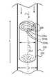
- FIG. 2illustrates a cartridge assembly 220 in a nanowire growth chamber 230 in accordance with one embodiment of the present invention.
- Cartridge assembly 220includes a coiled sheet of material having a plurality (n) of support layers 224 a, b, c . . . n , in which plurality of support layers 224 are spaced apart by a set distance 226 .
- “plurality”refers to two or more of an article (i.e., 2, 3, 4, 5, 10, 20, 30, 50, 100, 500, 1000 etc.).
- Each support layer 224has opposing first and second surfaces (see surfaces 1012 and 1014 of FIGS. 10 and 11 ) on which a plurality of catalysts are disposed (see catalysts 442 illustrated in FIG.
- cartridge assembly 220is cylindrical, having a diameter D, a length L, and a longitudinal axis 222 .
- FIG. 2shows cartridge assembly 220 inserted into growth chamber 230 , such as a CVD furnace, so that longitudinal axis 222 of cartridge assembly 220 is parallel with the longitudinal axis of growth chamber 230 .
- nanowire growth chamber 230has a cross-sectional shape that is substantially the same as the cross-sectional shape of cartridge assembly 220 .
- nanowire growth chamber 230has a diameter d that is only slightly larger than diameter D of cartridge assembly 220 .
- One or more precursor gasesare provided in nanowire growth chamber 230 , and flow in a direction f (as shown by the arrows illustrated in FIG. 2 ) that is parallel with longitudinal axis 222 and the surfaces of support layers 224 . It should be noted that flow direction f can also be in the opposite direction from that shown in FIG. 2 .
- the “set distance”is a predetermined distance between support layers that can vary about +/ ⁇ 20% from the predetermined distance to account for manufacturing error. Thus, the actual distance between the support layers may be in a range of about +/ ⁇ 20% of the predetermined distance.
- Support layers 224are preferably spaced apart substantially evenly, to ensure uniform exposure of the catalysts to the precursor gas flowing between the spaced-apart layers. In the embodiment shown in FIG. 11 , support layers 224 are spaced evenly apart (i.e., set distance 226 is substantially uniform), ensuring an even gas flow due to the uniformity of the spacing in the coil (i.e., cartridge assembly 220 ).
- a substantially uniform set distancemeans that the each set distance between adjacent support layers has a predetermined distance that is within about +/ ⁇ 20% of each other set distance between other adjacent support layers of the cartridge assembly.
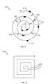
- Cartridge assembly 220has a cross-sectional shape that is substantially circular (see FIG. 11 ).
- substantially circularrefers to a curved shape in which every point on the curve is an equal distance from the center of the cross-section (i.e., uniform radii), or in which these distances vary by no more than a few % to about 20% across the curved shape.
- a substantially circular cross-sectionalso includes oval cross-sections.
- cartridge assembly 220can have a cross-sectional shape that is substantially rectangular or polygonal, and can be formed in a shape that corresponds with the cross-sectional shape of a given nanowire growth chamber.
- Cartridge assembly 220can be any diameter D and length L, limited only by the dimensions of growth chamber 230 in which it is ultimately to be used.
- diameter Dmay range between 1-200 cm in one embodiment, 5-100 cm in another embodiment, 5-70 cm in another embodiment, and 7-60 cm in another embodiment.
- length Lmay range between 1-200 cm in one embodiment, 3-150 cm in another embodiment, 5-75 cm in another embodiment, and 7-60 cm in another embodiment.
- a cartridge assembly of diameter D of 7.5 cm and length L of 10 cmwhich is formed from coiling a sheet of material having a thickness of about 1.27 ⁇ m (0.0005 inches) and with the plurality of support layers being separated by a set distance of 30 ⁇ m, will have a total surface area for nanowire growth approaching 10 m 2 .
- Nanowireswill grow from the surfaces of support layers 224 (see nanowires 440 illustrated in FIG. 11 ).
- cartridge assembly 220can be removed from growth chamber 230 , and the nanowires harvested, such as by sonication or mechanical means, or any other means known to one of skill in the art.
- Cartridge assembly 220can then be cleaned and reused if desired, or the material of cartridge assembly can be recycled.
- cartridge assembly 220provides easy handling, while still providing a high surface area in comparison with the conventional fluidized bed approach for growing a high density of nanowires.
- precursor gasmay be provided in a first direction for a first period of time (i.e., at the top end of from the bottom end of cartridge assembly 220 as shown in FIG.
- Other optimization techniquesmay include, for example, manipulating the heating profile along the longitudinal axis 222 of cartridge assembly 220 as well as preheating the precursor gas prior to providing it in the growth chamber 230 .
- a cartridge assembly 320is formed from a sheet of material coiled in a cone shape, in which there is a smaller diameter at one end of the coiled sheet than a diameter at an opposite end of the coiled sheet.
- cartridge assembly 320is provided with a plurality of support layers 324 which are spaced apart at a smaller diameter end 320 b of the coiled sheet by a spacing distance (set distance) 326 b that is less than a spacing distance 326 a between support layers 324 at an opposite, larger diameter end 320 a .
- the precursor gascan be provided to flow parallel with longitudinal axis 222 of cartridge assembly 320 , in the direction f as shown by the arrows illustrated in FIG. 3 (or can be in the opposite direction).
- the precursor gasflows from larger diameter end 320 a to smaller diameter end 320 b .
- larger spacing distance 326 a between layers at larger diameter end 320 aensures there is less resistance to gas flow by the growing nanowires.
- spacing distance 326 between adjacent layers 324 at smaller diameter end 320 bcorrelates with a reduced surface area of each layer 324 at smaller diameter end 320 b . Consequently, a reduced amount of the precursor gas may be required at smaller diameter end 320 b , than at larger diameter end 320 a .
- spacing distance 326 between layers at that sectioncan be configured to be substantially uniform (resembling the uniform spacing illustrated in the axial view of cartridge assembly 220 of FIG. 11 ). The substantially uniform spacing ensures uniform exposure of the catalyst and growing wires to the precursor gas at a given cross section of the cartridge assembly 320 .
- a growth chambermay have a rectangular cross-section, rather than circular, and in this instance the methods of the present invention may include providing a cartridge assembly that has a corresponding rectangular shape.
- cartridge assembly 220can have a rectangular cross-section (see, e.g., FIG. 12 , illustrating a rectangular cartridge assembly 1220 comprised of a coiled sheet of material forming a plurality of support layers 1224 ).
- a rectangular cartridge assemblyhas a plurality of parallel plates, as illustrated in FIGS. 4 and 5 .
- a cartridge assembly 420includes a plurality (n) of parallel plates 424 a - d , . . . n, in which each plate 424 has opposing first and second surfaces 412 , 414 (see FIG. 5 ).
- parallel plates 424are spaced apart by a set distance 426 a , and a plurality of catalysts 442 may be disposed on one or both surfaces 412 , 414 .
- Cartridge assembly 420is inserted into a rectangular growth chamber 530 and oriented so that the precursor gas can flow parallel to surfaces 412 , 414 , in a direction f illustrated by the arrows (or can be in the opposite direction).
- the precursor gaswill pass through the spacing between the plurality of parallel plates 424 and nanowires will grow from surfaces 412 , 414 on which catalysts were disposed.
- the set distance 426 between the parallel plates 424is preferably substantially uniform, to ensure an even gas flow between the support layers and uniform exposure of the catalysts and growing wires 440 .
- cartridge assembly 420can be removed from growth camber 530 , and nanowires 440 harvested.
- FIGS. 6A , 6 B, 7 and 8illustrate exemplary mesh screens 624 provided as a support layers. Each screen 624 has opposing first and second surfaces 612 , 814 with a plurality of apertures 608 . A plurality of nanowire catalysts can be disposed on either or both surfaces 814 and 612 , as well as in each aperture 608 . As illustrated in the enlarged views of FIGS. 6A and 6B , nanowires 640 may grow on surface 612 of screen 624 (provided that catalysts are disposed thereon).
- Nanowirescan also grow into an interior surface 606 of aperture 608 . Further, nanowires can grow on opposing surface 814 (see FIG. 8 ) (provided that catalysts are provided thereon). Thus, the mesh screen offers an increased surface area for possible nanowire growth, including not only surfaces 612 and 814 , but also interior surface 606 of each aperture 608 .
- a precursor gasmay be provided in a flow direction f, so as to be parallel with the surface of each mesh screen 624 .
- the precursor gasmay be provided perpendicular to surfaces 612 and 814 , in a flow direction f, as illustrated by its respective arrow in FIG. 7 .
- the precursor gas flowis likely to be more turbulent than in the former example, as it will be disrupted by screen 624 and forced to flow through apertures 608 .
- FIG. 8A plurality of spaced-apart parallel mesh screens comprise a cartridge assembly that is placed in a nanowire growth chamber 830 . Precursor gas flows in direction f, perpendicular to surfaces 612 and 814 , through apertures 608 .
- FIG. 9provides a flowchart of a method 900 for making a nanowire growth cartridge assembly 220 .
- Method 900includes steps 910 , 920 and 930 .
- step 910a sheet of material is embossed to generate spacers.
- step 920the sheet of material is formed into a coiled sheet of material having a plurality of support layers that are spaced apart by the spacers.
- step 930catalysts are disposed on one or both opposing surfaces of each support layer. Reference is made to FIG.
- Sheet of material 1000is suitably placed through a stamping machine (not shown) to emboss surface 1014 to create a plurality of spaced protrusions, or nubs, which form spacers 1050 , protruding from opposing surface 1012 .
- the surfacemay be crimped to have a corrugated pattern or to have intermittent folds which can serve as spacers 1050 .
- sheet of material 1000has been manipulated after embossing to form a coil so as to have the plurality of support layers 224 spaced apart by spacers 1050 .
- the heights 1052 of each spacer 1050is substantially the same as the set distance 226 that separates adjacent support layers 224 , and ensures that support layers 224 are separated by set distance 226 .
- a sheet of materialis easily formed to include spacers so that the sheet can be coiled to form support layers 224 that are guaranteed to be spaced apart by set distance.
- Spacing between support layersmay range between 10-1000 lam in one embodiment, 20-500 ⁇ m in another embodiment, 20-100 ⁇ m in another embodiment, and 30-50 ⁇ m in another embodiment.
- the spacing between adjacent support layers 224may be about 50 ⁇ m, with corresponding spacers of about 50 ⁇ m, and in another example the spacing 224 may be about 30 ⁇ m, with corresponding spacers of about 30 ⁇ m.
- spacersare provided on only a few percent of the surface area of sheet material 1000 , for example from 2-10%, from 3-8%, from 2-5%, or from less than 1%.
- heights 1052 of each spacer 1050may be substantially the same, thereby ensuring a uniform spacing between plurality of support layers 224 of cartridge assembly 220 .
- the heights 1052vary.
- the heightsmay vary along sheet of material 1000 in a configuration such that the spacing varies radially between adjacent support layers.
- the outer layers of the coilmay be closer together than the inner layers, or vice versa.
- the heights of spacersmay range from about one to about five times the length of the nanowires that are desired to be grown on the surface of the sheet of material 1000 .
- spacers 1050may be used as spacers 1050 to separate support layers by the set distance.
- spacers 1050may be used as spacers 1050 to separate support layers by the set distance.
- spacers 1050may or may not be removed from the sheet of material after it is coiled into cartridge assembly 220 .
- catalystscan be disposed onto surfaces 1012 and/or 1014 of sheet material 1000 prior to coiling the sheet.
- sheet of material 1000is coiled prior to disposing the catalysts.
- several methods for disposing catalysts onto nanowire growth substratesmay be used.
- aluminum foilmay be used as sheet of material 1000 . The foil is boiled for approximately 10 minutes, so as to convert the surface to aluminum trihydrate, and then the coil is dried and placed in a solution of gold colloid, which sticks to the surface. The aluminum coil is then dried off and the coil is tightened prior to being placed into the growth chamber (e.g., growth chamber 230 ).
- This processmay also be made continuous, as a roll-to-roll process, in which sheet material 1000 is (i) unwound from coil 1100 (see FIG. 10 ), (ii) sent through an embossing machine to generate spacers 1050 integrally on surface 1012 of sheet 100 , (iii) boiled, (iv) dried, then (v) gold colloid is disposed thereon, then (vi) dried and (vii) recoiled, to form cartridge assembly 220 .
- catalystsmay be disposed using polylysine as an adhesive layer, electrophoresis, or a gold film may be disposed on one or both surfaces 1012 , 1014 , and heat then applied that causes the colloid to coalesce and form droplets of catalysts.
- nanowiresmay grow over the course of a few hours. For example, one run using an 8 inch coil cartridge may produce 100-200 grams, whereby five runs produces about one kilogram of nanowires. For fuel cell catalysts, for example, a gram of nanowires is often needed. Thus, it should be apparent that bulk nanowire production is achieved by the apparatus and methods of the present invention.
- the coiled sheetmay be unrolled prior to removal of the nanowires.
- the nanowiresmay be harvested directly from coiled sheet, with the sheet remaining coiled.
- Sonication or mechanical means, or any other means known to one of skill in the artmay be used to harvest the nanowires.
- the sheet of material with nanowiresis immersed in a solution bath (e.g., a bath of isopropyl alcohol (IPA)) and subjected to ultrasonic waves from ultrasonic transducers, whereby the nanowires are detached from the sheet of material and are collected in the bath.
- IPAisopropyl alcohol
- a subsequent filtration stepmay then be employed to separate the nanowires from the solution (IPA).
- the nanowires and IPA mixturemay be filtered under pressure through a micron filter (e.g., 0.4 micron filter), with the nanowires being collected by the filter.
- the collected filter mat of nanowiresmay then be dried.
- An exemplary sonication method of harvesting the nanowires from the unrolled coiled sheetis described later with reference to FIG. 21 .
- Sheet of material 1000is suitably as thin as possible to maximize the surface area available for a nanowire growth.
- a sheet of materialmay have a thickness in the range of less than about 1 mm, and in other embodiments, the sheet of material has a thickness of about 0.5 to about 1 mm, about 5 to about 50 ⁇ m, or about 10-20 ⁇ m.
- Sheet of materialmay be any suitable material including glass, polymers, ceramics or metals.
- Sheet of material 1000is not required to be of crystalline structure, but should withstand a high temperature in a CVD furnace, as well as the temperature necessary for disposition of the catalysts.
- sheet of material 1000may also be a flexible mesh wire mesh material that may be rolled into a coil.
- a stainless steel sheetis used that is 0.00127 cm thick and 10 cm wide. Such a sheet can be provided with 30 ⁇ m protrusion to make a cylindrical cartridge assembly having a 7.5 cm diameter and 10 centimeters in length, with the available surface area for nanowire growth approaching 10 m 2 .
- cartridge assembly 220has a 7.62 cm diameter D and an 20.32 cm length L.
- the present inventionis scalable, such that increasing the size of the cartridge assembly should increase the total weight of nanowires that may be harvested therefrom.
- an 20.32 cm diameter cartridge assembly 220being about 0.3 m to 0.6 m in length may produce between 0.5 to 1 kilograms of nanowires in bulk.
- size of cartridge assembly 220may be optimized for ease of handling. For example, it may be decided that it is more desirable to have multiple smaller tubes in a large growth chamber 230 , rather than one large tube. Further, there may be production issues that arise as the cartridge increases in size, such as, for example, heat uniformity issues.
- catalystsmay be disposed on one or both opposing surfaces of each support layer of the cartridge assembly.
- the density of disposed catalystsmay be selected as desired, such as, for example, 1 to 100 particles/cm 2 . In other embodiments, the density can be, for example, 1 to 500 particles/cm 2 , or 100 to 500 particles/cm 2 . Further, the catalysts can be disposed uniformly on each surface or may be disposed in a pattern.
- FIG. 13illustrates an example of a patterned disposition of catalysts 1390 on a surface 1312 of an exemplary support layer 1324 .
- Support layer 1324may be one of the plurality of support layers 424 of cartridge assembly 420 with parallel plates (see FIG.
- a masking 1321is suitably provided on surface 1312 of support layer 1324 in the region where nanowire growth is not desired prior to disposing the catalyst on the surface.
- Masking 1321may be any film or other material layer to which catalysts 1390 will not adhere to, such that catalysts 1390 are disposed only the surface of 1324 in the regions where masking 1321 is absent.
- a cartridge assembly 1420 in accordance with the present inventioncan be comprised of a plurality of parallel tubes 1424 .
- Each tube 1424has an inner surface 1412 and an outer surface 1414 on which catalysts may be disposed.
- This cartridge of tubes 1424may be placed in a nanowire growth chamber, and the precursor gas may be provided in a flow direction that is perpendicular to the longitudinal axes of tubes 1424 , or in a flow direction that is parallel with the longitudinal axes of tubes 1424 .
- the precursor gasmay be provided in a flow direction that is perpendicular to the longitudinal axes of tubes 1424 , or in a flow direction that is parallel with the longitudinal axes of tubes 1424 .
- a cartridge assembly 1520can be comprised of a plurality of concentric tubes 1524 , each surface of each tube 1524 serving as a support layer for nanowire growth.
- the cartridge assemblies of the present inventionas nanowire growth supports, an efficient use of the precursor gas can be achieved and nanowire growth can be maximized for the available surface area and growth chamber volume.
- gas flow, gas concentration temperature, and gas flow directionsmay be optimized to ensure uniform exposure of the catalysts and growing nanowires, and efficient use of the precursor gas.
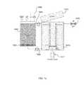
- flowchart 1600provides exemplary production methods for nanowire manufacturing.
- the methods of flowchart 1600suitably comprise step 1602 , in which an aluminum foil is embossed.
- step 1604 of flowchart 1600the foil is then cleaned, and in step 1606 a substrate surface is prepared (e.g., a metal, polymer, carbon or other substrate).
- Gold colloidis disposed on the substrate in step 1608 , followed by drying in step 1610 .
- Nanowire growthis then performed in step 1612 using a VLS-process (other processes as described herein can also be used).
- the nanowiresare then harvested (for example, by sonication) in step 1614 , filtered in step 1616 and dried in step 1618 .
- the nanowirescan then be ball milled in step 1620 to break the nanowires into short segments, which may be used, for example, as additives in a battery slurry as described in U.S. Provisional Patent Application No. 61/221,392, filed Jun. 29, 2009, entitled, “Nanostructured Materials for Battery Applications,” the disclosure of which is incorporated by reference herein.
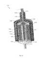
- the embossed aluminum foil having an embossed profile 1713 on its surfacecan be formed into a coil that serves as a cartridge assembly 1720 to facilitate preparation of a large number of nanowires, in accordance with the present invention.
- FIG. 18shows an embossing apparatus 1880 which may be used for step 1602 to emboss the aluminum foil. Specifically, a coil of aluminum foil 1100 is unwound to form an uncoiled sheet of foil 1000 that is suitably placed through embossing apparatus 1880 to provide embossed profile 1713 on the foil's surface.
- Embossing apparatus 1880includes a left-handed helical die roll 1881 , a right-handed helical die roll 1882 , and a nip roll 1884 .
- Foil 1000is sandwiched between the rolls, with the die rolls 1881 , 1882 disposed against a first surface of foil 1000 and nip roll 1884 disposed against the opposing second surface of foil 1000 .
- a suitable pressureis applied by rolls 1881 , 1882 , and 1884 against the surfaces of foil 1000 such that foil 1000 is embossed to have embossed profile 1713 .
- Foil 1000is rewound after embossing to form cartridge assembly 1720 .
- Embossed profile 1713serves as spacers that maintain a substantially uniform space between layers of the coiled foil that form cartridge assembly 1720 .
- Cleaning of the foil in step 1604may be achieved by immersing the foil in a standard chemical immersion apparatus.
- the foilmay immersed in a bath of IPA.
- the surfaces of cartridge assembly 1720may be prepared for disposing gold colloid thereon in step 1608 .
- Surface preparation of cartridge assembly 1720may be achieved by subjecting cartridge assembly 1720 to a hot water treatment process using the apparatus illustrated in FIG. 19 . Hot water may be used to convert the cartridge's surfaces from metallic aluminum to hydroxylated or hydrated alumina, to which the gold colloid is attracted.
- FIG. 19includes a reservoir 1960 provided with a heater 1964 and a vacuum 1966 , and a surface preparation tank 1970 in fluid communication with reservoir 1960 via an inlet valve 1962 and a return valve 1968 .
- Surface preparation tank 1970is provided with a cover 1972 , a vacuum valve 1976 , and a stirrer 1977 for circulating hot water in the tank.
- cartridge assembly 1720is placed in surface preparation tank 1970 and cover 1972 is closed.
- Vacuum 1966is then operated to eliminated air bubbles in the water contained in reservoir 1960
- vacuum valve 1976is operated to eliminate air bubbles trapped between foil layers in cartridge assembly 1720 .
- Both inlet valve 1962 and outlet valve 1968are then opened, and the water, heated by heater 1964 , is circulated through surface preparation tank 1970 , entering surface preparation tank 1970 via inlet valve 1962 , and exiting via return valve 1968 .
- Disposing gold colloid (step 1608 ) on cartridge assembly 1720may be achieved using the apparatus illustrated in FIG. 20 .
- This apparatusincludes a reservoir 2060 provided with a vacuum 2066 , and a disposition tank 2070 in fluid communication with reservoir 2060 via an inlet valve 2062 and a return valve 2068 .
- Disposition tank 2070is provided with a cover 2072 , a vacuum valve 2076 , and a stirrer 2077 for circulating gold colloid in the tank.
- cartridge assembly 1720 which has been surface-treated in step 1606is disposed in tank 2070 and cover 2072 is closed.
- Vacuum 2066is then operated to eliminated air bubbles in the gold colloid contained in reservoir 2060 , and vacuum valve 2076 is operated to eliminate any air bubbles trapped between foil layers in cartridge assembly 1720 .
- Both inlet valve 2062 and outlet valve 2068are then opened, and the gold colloid is circulated through disposition tank 2070 , entering the tank via inlet valve 2062 , and exiting via return valve 2068 .
- cartridge assembly 1720is dried (step 1610 ). Drying may be achieved by loading the cartridge assembly in a nanowire growth chamber, and flushing the chamber with high velocity hot air. Hot air may be used in combination with other heaters (such as a heating coil which heats the cartridge assembly in the chamber).
- a precursor gasis applied to the chamber to grow nanowires on the surfaces of each layer of cartridge assembly 1720 (step 1612 ).
- the chambermay be purged of the precursor gas and cartridge assembly 1720 cooled.
- FIG. 21illustrates a schematic (shown in cross-section) of cartridge assembly 1720 loaded in an exemplary nanowire growth chamber 2130 for growing nanowires (step 1612 ).
- Chamber 2130may also be used for the pre-growth process of drying and the post-growth process of cooling.
- Chamber 2130includes an outer enclosure 2134 within which is disposed insulation 2136 , a gas heater coil 2184 , a blanket heater coil 2186 , and a process heater coil 2188 (each of which may be cooling coils if the chamber is intended for use in post-growth process cooling).
- Cartridge assembly 1720is loaded at loading platform 2139 at the bottom of chamber 2130 , and a housing 2138 covers a top of cartridge assembly 1720 in chamber 2130 .
- a holding bolt 2199holds cartridge assembly 1720 sandwiched between loading platform 2139 and top housing 2138 .
- a piston seal 2198separates the heater coils from cartridge assembly 1720 , and a seal gasket 2196 provides a seal were loading platform 2139 connects to enclosure 2134 .
- Loading platform 2139 , top housing 2138 , and piston seal 2198define an inner chamber in which cartridge assembly 1720 is disposed and through which gas flows.
- Blanket heater coil 2186surrounds a top of cartridge assembly 1720 and process heater coil 2188 surrounds sides of cartridge assembly 1720 .
- the gas flow direction f through the chamber 2130is illustrated by the arrows in FIG. 21 . As shown, the gas flow direction is parallel with a longitudinal axis of cartridge assembly 1720 .
- the gas usedis a suitable precursor gas, whereby nanowires grow from gold colloid catalysts disposed on the layers of cartridge assembly 1720 . If chamber 2130 is used for the pre-growth process of drying (step 1610 ) or the post-growth process of cooling, then the gas used may be air, for example.
- FIG. 22illustrates a schematic of an exemplary apparatus for harvesting nanowires from cartridge assembly 1720 (step 1614 ) using a sonication process.
- the harvesting apparatusincludes a harvesting tank 2256 filled with a solvent such as IPA.
- Tank 2256is placed in an outer tank 2258 filled with distilled H 2 O (DI-H 2 O).
- DI-H 2 Odistilled H 2 O
- At the bottom of outer tank 2258are one or more ultrasonic transducers 2259 .
- the tank within another tankis used for improving the safety of the sonication process, but is not necessary.
- cartridge assembly 1720is unwound such that sheet of material 1000 with nanowires thereon (not shown) is passed through harvesting tank 2256 via multiple rollers 2291 , 2292 , 2293 , and 2294 .
- Rollers 2292 and 2293reside within harvesting tank 2256 and serve to keep material 1000 immersed in the IPA while being subjected to the ultrasonic waves from transducers 2259 .
- Flat spray manifolds 2295are provided to spray the opposing surfaces of material 1000 as it exits harvesting tank 2256 , so as to remove nanowires still connected to the of surface material 1000 after sonication.
- material 1000is rewound into a coil 2220 which can be cleaned and reused as a cartridge assembly, or can be recycled.
- Nanowire growth trialswere conducted using a process in accordance with the present invention.
- the processincluded 12 process stages, which include Aluminum foil substrate mechanical pre-patterning (stage 1); Pre-cleaning in IPA (stage 2); Hot distilled H 2 O (DI-H 2 O) hydroxylation/oxidation treatment (stage 3); Triple DI-H 2 O rinsing (stage 4); Gold nanoparticle disposition (stage 5); Triple DI-H 2 O rinsing (stage 6); IPA rinsing (stage 7); Oven drying (stage 8); CVD nanowire growth (stage 9); Wire harvesting (stage 10); Filtration (stage 11); and Drying (stage 12). Further details on the process stages is provided below. A summary of the trial data for Trial runs 202-051 and 202-057 is presented in Table 1.
- This stageinvolved producing sheets of aluminum (Al) with integral spacers which creates the necessary space between adjacent layers of sheet when coiled to ensure both liquid disposition of Au nanoparticles (from an Au colloid solution) and subsequent growth of Si NWs (from silane gas decomposition in a CVD furnace).
- Alaluminum
- one Al sheetwas 8 inches (20.32 cm) wide, 2.0 mil thick, 1100 alloy hard-tempered “H19” (1100-H19 from AllFoils, Inc.) and was deformed while passing through stainless steel rollers to produce a corrugation pattern with amplitude of about 0.9 mm.
- a second Al sheet that was 6 inches (15.24 cm) widewas embossed with dots. The second Al sheet was placed on the first AL sheet, and the sheets were rolled together to form a single coil.
- stage 2the coil is pre-cleaned in IPA, by placing the coil vertically in a bath of IPA and subjecting the bath to 170 KHz sonication.
- stage 3the coiled is subjected to a hot hydroxylation/oxidation treatment.
- the coilis placed in a bath of distilled H 2 O (DI-H 2 O) at 60° C. whereby the Al substrate surfaces are chemically converted from metallic aluminum to hydroxylated or hydrated alumina to ensure they are positively charged.
- DI-H 2 Odistilled H 2 O
- gold catalyst nanoparticlesare disposed on the surfaces of the coil by soaking the coil in an aqueous suspensions of 0.01% Au chloride in DI-H 2 O.
- the negatively charged Au catalyst particles (HAuCl 4 ) in the colloidare electrostaticly attracted to the positively charged alumina coil surfaces and substantially uniformly deposit on the surfaces.
- the colloidal solutionsmay range between 10%-70% Au Colloid (0.01% Au Chloride) in DI-H 2 O.
- 60 nm size gold particleswere disposed
- Trial run 202-05720 nm size gold particles were disposed on the surfaces.
- FIGS. 25A and 25Bshow SEM micrographs of 60 nm Au nanoparticles on the alumina coil surface from Trial run 202-051.
- FIGS. 27A and 27Bshow SEM micrographs of 20 nm Au nanoparticles on the alumina coil surface from Trial run 202-057.
- a colloidal aqueous suspension(0.01% Au Chloride) available commercially from BB International (British Biocell) was diluted to a solution of 30% Au Colloid (0.01% Au Chloride) in DI-H 2 O.
- stage 6the coil was tripled rinsed in DI-H 2 O, and in stage 7, the coil was rinsed in IPA. In stage 8, the coil was oven dried at 110° C.
- FIG. 23illustrates an Au-nanoparticle treated corrugated coil 2320 being bottom-loaded into a furnace tube 2330 , in accordance with the present Example.
- Holding bolt 2199extends along the center axis of the coil 2320 .
- a foil piecemay be placed above holding bolt 2199 and used as a spacer to center the coil at the hot zone center (not shown) of the elongated furnace tube 2330 .
- FIG. 24illustrates an axial view of coil 2320 with holding bolt 2199 .
- silane gasSiH 4
- the gold nanoparticlesact as catalytic sites or seeds for the thermal, gas-phase CVD growth of crystalline silicon wires of the same diameter.
- Catalyst diameterdetermines nanowire diameter, and wire length is controlled by exposure time to the silane gas.
- nanowire growth rateis about 0.7 ⁇ m/min.
- FIGS. 26A-26Cshow SEM micrographs of 60 nm NWs grown on a coil surface, from Trial run 202-051.
- FIGS. 28A-28Dshow SEM micrographs of 20 nm NW grown on a coil surface from Trial run 202-057.
- the nanowiresare ultrasonically harvested (40 kHz sonication) by unwinding the coil and passing the unwound sheet of material through a bath of Di-H2O-10% IPA solution.
- the unwound sheetis placed close to a bottom surface of the bath in a horizontal orientation.
- the harvested 60 nm Si NWs in Di-H2O-10% IPA solution fromhad a yellow color
- the solution of 20 nm Si NWs harvested in Di-H2O-10% IPA solutionhad a brown color.
- stage 11the NWs were filtered from the Di-H2O-10% IPA solution using a laboratory vacuum filter flask having a paper filter.
- stage 11the NWs captured by the filter paper were dried and then separated from the filter paper.
Landscapes
- Chemical & Material Sciences (AREA)
- Engineering & Computer Science (AREA)
- Organic Chemistry (AREA)
- Materials Engineering (AREA)
- Chemical Kinetics & Catalysis (AREA)
- Nanotechnology (AREA)
- Crystallography & Structural Chemistry (AREA)
- Physics & Mathematics (AREA)
- Metallurgy (AREA)
- General Physics & Mathematics (AREA)
- Condensed Matter Physics & Semiconductors (AREA)
- Inorganic Chemistry (AREA)
- Thermal Sciences (AREA)
- Manufacturing & Machinery (AREA)
- Composite Materials (AREA)
- Catalysts (AREA)
Abstract
Description
| TABLE 1 | |||
| Run# 202- | |||
| -051 | -057 | |||
| 1100-H19 Al foils length (6″ & 8″): | ~11.1 ft | ~9.6 ft | ||
| Au Colloid size (nm) | 60 | 20 | ||
| Au Colloid Deposit Time (hrs in | 5.0 | 4.5 | ||
| diluted 0.01% Au Chloride)** | ||||
| Au NP density (per μm2) | 10.6 | 21.2 | ||
| Tube OD (in) | 3 | 3 | ||
| Surface area (m2): | 2.42 | 2.07 | ||
| NW Growth conditions: | ||||
| Total Pressure (torr): | 30 | 45 | ||
| Silane Partial Pressure (torr): | 1.7 | 4.8 | ||
| Silane Flow (sccm) | 50.2 | 75.2 | ||
| Hydrogen Flow (sccm) | 301 | 234 | ||
| Helium Flow (sccm) | 551 | 401 | ||
| TC Setpoint (° C.) | 455 | 450 | ||
| Total Gas Flow (sccm) | 902 | 711 | ||
| Calc. Gas Residence Time (sec)*** | 0.77 | 1.48 | ||
| Growth Time (min) | 60 | 100 | ||
| NW + Si Deposit wt gain (g): | 2.52 | 1.98 | ||
| (g/m2) | 1.04 | 0.96 | ||
| **Dilutions are 60% for 60 nm and 30% for 20 nm. | ||||
| ***neglecting cross-sectional area occupied by the foils | ||||
Claims (13)
Priority Applications (1)
| Application Number | Priority Date | Filing Date | Title |
|---|---|---|---|
| US12/824,485US8623288B1 (en) | 2009-06-29 | 2010-06-28 | Apparatus and methods for high density nanowire growth |
Applications Claiming Priority (2)
| Application Number | Priority Date | Filing Date | Title |
|---|---|---|---|
| US22150109P | 2009-06-29 | 2009-06-29 | |
| US12/824,485US8623288B1 (en) | 2009-06-29 | 2010-06-28 | Apparatus and methods for high density nanowire growth |
Publications (1)
| Publication Number | Publication Date |
|---|---|
| US8623288B1true US8623288B1 (en) | 2014-01-07 |
Family
ID=49840828
Family Applications (1)
| Application Number | Title | Priority Date | Filing Date |
|---|---|---|---|
| US12/824,485Active2032-11-07US8623288B1 (en) | 2009-06-29 | 2010-06-28 | Apparatus and methods for high density nanowire growth |
Country Status (1)
| Country | Link |
|---|---|
| US (1) | US8623288B1 (en) |
Cited By (5)
| Publication number | Priority date | Publication date | Assignee | Title |
|---|---|---|---|---|
| US20090255222A1 (en)* | 2007-07-10 | 2009-10-15 | Raul Cortez | Methods and apparatus for the in situ collection of nucleated particles |
| US20130092525A1 (en)* | 2007-07-10 | 2013-04-18 | Innovalight, Inc. | Concentric flow-through plasma reactor and methods therefor |
| US9812699B2 (en) | 2011-10-05 | 2017-11-07 | Oned Material Llc | Silicon nanostructure active materials for lithium ion batteries and processes, compositions, components and devices related thereto |
| US10243207B2 (en) | 2011-07-26 | 2019-03-26 | Oned Material Llc | Nanostructured battery active materials and methods of producing same |
| US10862114B2 (en) | 2016-07-15 | 2020-12-08 | Oned Material Llc | Manufacturing apparatus and method for making silicon nanowires on carbon based powders for use in batteries |
Citations (118)
| Publication number | Priority date | Publication date | Assignee | Title |
|---|---|---|---|---|
| US5196396A (en) | 1991-07-16 | 1993-03-23 | The President And Fellows Of Harvard College | Method of making a superconducting fullerene composition by reacting a fullerene with an alloy containing alkali metal |
| US5332910A (en) | 1991-03-22 | 1994-07-26 | Hitachi, Ltd. | Semiconductor optical device with nanowhiskers |
| US5505928A (en) | 1991-11-22 | 1996-04-09 | The Regents Of University Of California | Preparation of III-V semiconductor nanocrystals |
| US5512131A (en) | 1993-10-04 | 1996-04-30 | President And Fellows Of Harvard College | Formation of microstamped patterns on surfaces and derivative articles |
| US5674592A (en) | 1995-05-04 | 1997-10-07 | Minnesota Mining And Manufacturing Company | Functionalized nanostructured films |
| US5690807A (en) | 1995-08-03 | 1997-11-25 | Massachusetts Institute Of Technology | Method for producing semiconductor particles |
| US5840435A (en) | 1993-07-15 | 1998-11-24 | President And Fellows Of Harvard College | Covalent carbon nitride material comprising C2 N and formation method |
| US5858862A (en) | 1996-09-25 | 1999-01-12 | Sony Corporation | Process for producing quantum fine wire |
| US5897945A (en) | 1996-02-26 | 1999-04-27 | President And Fellows Of Harvard College | Metal oxide nanorods |
| US5962863A (en) | 1993-09-09 | 1999-10-05 | The United States Of America As Represented By The Secretary Of The Navy | Laterally disposed nanostructures of silicon on an insulating substrate |
| US5976957A (en) | 1996-10-28 | 1999-11-02 | Sony Corporation | Method of making silicon quantum wires on a substrate |
| US5997832A (en) | 1997-03-07 | 1999-12-07 | President And Fellows Of Harvard College | Preparation of carbide nanorods |
| US6036774A (en) | 1996-02-26 | 2000-03-14 | President And Fellows Of Harvard College | Method of producing metal oxide nanorods |
| US6048616A (en) | 1993-04-21 | 2000-04-11 | Philips Electronics N.A. Corp. | Encapsulated quantum sized doped semiconductor particles and method of manufacturing same |
| US6068800A (en) | 1995-09-07 | 2000-05-30 | The Penn State Research Foundation | Production of nano particles and tubes by laser liquid interaction |
| US6132874A (en) | 1995-08-22 | 2000-10-17 | Rhodia Chimie | Functionalized inorganic oxide hydroxylated carrier and method for preparing same |
| US6136156A (en) | 1996-03-01 | 2000-10-24 | Virginia Commonwealth University | Nanoparticles of silicon oxide alloys |
| US6146227A (en) | 1998-09-28 | 2000-11-14 | Xidex Corporation | Method for manufacturing carbon nanotubes as functional elements of MEMS devices |
| US6190634B1 (en) | 1995-06-07 | 2001-02-20 | President And Fellows Of Harvard College | Carbide nanomaterials |
| US6207229B1 (en) | 1997-11-13 | 2001-03-27 | Massachusetts Institute Of Technology | Highly luminescent color-selective materials and method of making thereof |
| US6225198B1 (en) | 2000-02-04 | 2001-05-01 | The Regents Of The University Of California | Process for forming shaped group II-VI semiconductor nanocrystals, and product formed using process |
| US6235675B1 (en) | 1998-09-22 | 2001-05-22 | Idaho Research Foundation, Inc. | Methods of forming materials containing carbon and boron, methods of forming catalysts, filaments comprising boron and carbon, and catalysts |
| US6256767B1 (en) | 1999-03-29 | 2001-07-03 | Hewlett-Packard Company | Demultiplexer for a molecular wire crossbar network (MWCN DEMUX) |
| US6261469B1 (en) | 1998-10-13 | 2001-07-17 | Honeywell International Inc. | Three dimensionally periodic structural assemblies on nanometer and longer scales |
| US6274007B1 (en) | 1999-11-25 | 2001-08-14 | Sceptre Electronics Limited | Methods of formation of a silicon nanostructure, a silicon quantum wire array and devices based thereon |
| US6294450B1 (en) | 2000-03-01 | 2001-09-25 | Hewlett-Packard Company | Nanoscale patterning for the formation of extensive wires |
| JP2001288626A (en) | 2000-04-03 | 2001-10-19 | Nissan Motor Co Ltd | Method for producing carbon nanofiber fixed body |
| US6306736B1 (en) | 2000-02-04 | 2001-10-23 | The Regents Of The University Of California | Process for forming shaped group III-V semiconductor nanocrystals, and product formed using process |
| US6306734B1 (en) | 1996-04-01 | 2001-10-23 | Evgeny Invievich Givargizov | Method and apparatus for growing oriented whisker arrays |
| US20010033796A1 (en) | 1999-06-28 | 2001-10-25 | Unger Marc A. | Microfabricated elastomeric valve and pump sysems |
| US20010051367A1 (en) | 1999-04-14 | 2001-12-13 | Ching-Hwa Kiang | Molecular nanowires from single walled carbon nanotubes |
| US20020004136A1 (en) | 1999-06-14 | 2002-01-10 | Yufei Gao | Carbon nanotubes on a substrate |
| US6339281B2 (en) | 2000-01-07 | 2002-01-15 | Samsung Sdi Co., Ltd. | Method for fabricating triode-structure carbon nanotube field emitter array |
| US20020014667A1 (en) | 2000-07-18 | 2002-02-07 | Shin Jin Koog | Method of horizontally growing carbon nanotubes and field effect transistor using the carbon nanotubes grown by the method |
| US6380103B2 (en) | 1996-01-03 | 2002-04-30 | Micron Technology, Inc. | Rapid thermal etch and rapid thermal oxidation |
| US20020072577A1 (en) | 2000-10-04 | 2002-06-13 | The Dow Chemical Company | Supported catalyst compositions |
| US6413489B1 (en) | 1997-04-15 | 2002-07-02 | Massachusetts Institute Of Technology | Synthesis of nanometer-sized particles by reverse micelle mediated techniques |
| US20020127495A1 (en) | 2001-03-12 | 2002-09-12 | Axel Scherer | Method of fabricating nanometer-scale flowchannels and trenches with self-aligned electrodes and the structures formed by the same |
| US20020130353A1 (en) | 1999-07-02 | 2002-09-19 | Lieber Charles M. | Nanoscopic wire-based devices, arrays, and methods of their manufacture |
| US20020130311A1 (en) | 2000-08-22 | 2002-09-19 | Lieber Charles M. | Doped elongated semiconductors, growing such semiconductors, devices including such semiconductors and fabricating such devices |
| US6465132B1 (en) | 1999-07-22 | 2002-10-15 | Agere Systems Guardian Corp. | Article comprising small diameter nanowires and method for making the same |
| US6471761B2 (en) | 2000-04-21 | 2002-10-29 | University Of New Mexico | Prototyping of patterned functional nanostructures |
| US20020158342A1 (en) | 2001-03-14 | 2002-10-31 | Mark Tuominen | Nanofabrication |
| US20020172820A1 (en) | 2001-03-30 | 2002-11-21 | The Regents Of The University Of California | Methods of fabricating nanostructures and nanowires and devices fabricated therefrom |
| US20020179434A1 (en) | 1998-08-14 | 2002-12-05 | The Board Of Trustees Of The Leland Stanford Junior University | Carbon nanotube devices |
| US6495258B1 (en) | 2000-09-20 | 2002-12-17 | Auburn University | Structures with high number density of carbon nanotubes and 3-dimensional distribution |
| US6515325B1 (en) | 2002-03-06 | 2003-02-04 | Micron Technology, Inc. | Nanotube semiconductor devices and methods for making the same |
| US20030037675A1 (en) | 2000-09-05 | 2003-02-27 | Gillingham Gary R. | Air filtration arrangements having fluted media constructions and methods |
| US20030044777A1 (en) | 1993-10-28 | 2003-03-06 | Kenneth L. Beattie | Flowthrough devices for multiple discrete binding reactions |
| US20030071246A1 (en) | 2001-01-23 | 2003-04-17 | Grigorov Leonid N. | Quantum devices based on crystallized electron pairs and methods for their manufacture and use |
| US20030089899A1 (en) | 2000-08-22 | 2003-05-15 | Lieber Charles M. | Nanoscale wires and related devices |
| US6586785B2 (en) | 2000-06-29 | 2003-07-01 | California Institute Of Technology | Aerosol silicon nanoparticles for use in semiconductor device fabrication |
| US20030121887A1 (en) | 2001-03-22 | 2003-07-03 | Garvey James F. | Multi-component substances and processes for preparation thereof |
| US20030184357A1 (en) | 2002-02-19 | 2003-10-02 | Commissariat A L'energie Atomique | Cathode structure with emissive layer formed on a resistive layer |
| US20030186522A1 (en) | 2002-04-02 | 2003-10-02 | Nanosys, Inc. | Methods of positioning and/or orienting nanostructures |
| US20030185741A1 (en) | 2001-04-06 | 2003-10-02 | Krzysztof Matyjaszewski | Process for the preparation of nanostructured materials |
| US20030189202A1 (en) | 2002-04-05 | 2003-10-09 | Jun Li | Nanowire devices and methods of fabrication |
| US20030195611A1 (en) | 2002-04-11 | 2003-10-16 | Greenhalgh Skott E. | Covering and method using electrospinning of very small fibers |
| US20030200521A1 (en) | 2002-01-18 | 2003-10-23 | California Institute Of Technology | Array-based architecture for molecular electronics |
| US6656573B2 (en) | 2001-06-26 | 2003-12-02 | Hewlett-Packard Development Company, L.P. | Method to grow self-assembled epitaxial nanowires |
| US20030222019A1 (en) | 2002-05-28 | 2003-12-04 | Battelle Memorial Institute | Electrostatic deposition of particles generated from rapid expansion of supercritical fluid solutions |
| US20030232721A1 (en) | 2002-01-31 | 2003-12-18 | Hydrocarbon Technologies Inc. | Supported noble metal nanometer catalyst particles containing controlled (111) crystal face exposure |
| US20040005258A1 (en) | 2001-12-12 | 2004-01-08 | Fonash Stephen J. | Chemical reactor templates: sacrificial layer fabrication and template use |
| US20040026684A1 (en) | 2002-04-02 | 2004-02-12 | Nanosys, Inc. | Nanowire heterostructures for encoding information |
| US20040063839A1 (en) | 2002-09-26 | 2004-04-01 | Canon Kabushiki Kaisha | Method of producing electron emitting device using carbon fiber, electron source and image forming apparatus, and ink for producing carbon fiber |
| US20040061422A1 (en) | 2002-09-26 | 2004-04-01 | International Business Machines Corporation | System and method for molecular optical emission |
| US20040095658A1 (en) | 2002-09-05 | 2004-05-20 | Nanosys, Inc. | Nanocomposites |
| US20040112964A1 (en) | 2002-09-30 | 2004-06-17 | Nanosys, Inc. | Applications of nano-enabled large area macroelectronic substrates incorporating nanowires and nanowire composites |
| US20040121681A1 (en) | 2002-12-23 | 2004-06-24 | Kimberly-Clark Worldwide, Inc. | Absorbent articles containing an activated carbon substrate |
| US20040118448A1 (en) | 2002-09-05 | 2004-06-24 | Nanosys, Inc. | Nanostructure and nanocomposite based compositions and photovoltaic devices |
| US20040135951A1 (en) | 2002-09-30 | 2004-07-15 | Dave Stumbo | Integrated displays using nanowire transistors |
| US20040147098A1 (en) | 2002-11-22 | 2004-07-29 | Frederic Mazen | Method for forming, by CVD, nanostructures of semi-conductor material of homogeneous and controlled size on dielectric material |
| US20040146560A1 (en) | 2002-09-05 | 2004-07-29 | Nanosys, Inc. | Oriented nanostructures and methods of preparing |
| US6773616B1 (en) | 2001-11-13 | 2004-08-10 | Hewlett-Packard Development Company, L.P. | Formation of nanoscale wires |
| US6790425B1 (en) | 1999-10-27 | 2004-09-14 | Wiliam Marsh Rice University | Macroscopic ordered assembly of carbon nanotubes |
| US20040206448A1 (en) | 2003-04-17 | 2004-10-21 | Nanosys, Inc. | Structures, systems and methods for joining articles and materials and uses therefor |
| US6808605B2 (en) | 2001-10-15 | 2004-10-26 | Korea Institute Of Science And Technology | Fabrication method of metallic nanowires |
| US20040213307A1 (en) | 2002-07-19 | 2004-10-28 | President And Fellows Of Harvard College | Nanoscale coherent optical components |
| US6831017B1 (en) | 2002-04-05 | 2004-12-14 | Integrated Nanosystems, Inc. | Catalyst patterning for nanowire devices |
| US20050011431A1 (en) | 2003-04-04 | 2005-01-20 | Btg International Limited | Precisely positioned nanowhiskers and nanowhisker arrays and method for preparing them |
| US6846565B2 (en) | 2001-07-02 | 2005-01-25 | Board Of Regents, The University Of Texas System | Light-emitting nanoparticles and method of making same |
| WO2004032193A3 (en) | 2002-09-30 | 2005-01-27 | Nanosys Inc | Large-area nanoenabled macroelectronic substrates and uses therefor |
| US20050026526A1 (en) | 2003-07-30 | 2005-02-03 | Verdegan Barry M. | High performance filter media with internal nanofiber structure and manufacturing methodology |
| US20050029678A1 (en) | 2003-07-08 | 2005-02-10 | University Of Texas System, Board Of Regents | Growth of single crystal nanowires |
| US20050038498A1 (en) | 2003-04-17 | 2005-02-17 | Nanosys, Inc. | Medical device applications of nanostructured surfaces |
| US20050062033A1 (en) | 2003-08-08 | 2005-03-24 | Canon Kabushiki Kaisha | Structure and method for production of the same |
| US20050066883A1 (en) | 2003-09-25 | 2005-03-31 | Nanosys, Inc. | Methods, devices and compositions for depositing and orienting nanostructures |
| US20050079659A1 (en) | 2002-09-30 | 2005-04-14 | Nanosys, Inc. | Large-area nanoenabled macroelectronic substrates and uses therefor |
| US20050089467A1 (en) | 2003-10-22 | 2005-04-28 | International Business Machines Corporation | Control of carbon nanotube diameter using CVD or PECVD growth |
| US6888208B2 (en) | 2003-07-30 | 2005-05-03 | Hewlett-Packard Development Company, L.P. | Square-law detector based on spin injection and nanowires |
| WO2004032191A3 (en) | 2002-09-30 | 2005-06-02 | Nanosys Inc | Applications of nano-enabled large area macroelectronic substrates incorporating nanowires and nanowire composites |
| WO2005023923A3 (en) | 2003-09-04 | 2005-06-16 | Nanosys Inc | Methods of processing nanocrystals, and compositions, devices and systems including same |
| US20050145596A1 (en) | 2003-12-29 | 2005-07-07 | Metz Matthew V. | Method of fabricating multiple nanowires of uniform length from a single catalytic nanoparticle |
| US20050176228A1 (en) | 2003-12-11 | 2005-08-11 | Fonash Stephen J. | Controlled nanowire growth in permanent, integrated nano-templates and methods of fabricating sensor and transducer structures |
| US20050181195A1 (en) | 2003-04-28 | 2005-08-18 | Nanosys, Inc. | Super-hydrophobic surfaces, methods of their construction and uses therefor |
| US20050187605A1 (en) | 2002-04-11 | 2005-08-25 | Greenhalgh Skott E. | Electrospun skin capable of controlling drug release rates and method |
| US20050191774A1 (en) | 2002-10-28 | 2005-09-01 | Zhiyong Li | Photonic crystals with nanowire-based fabrication |
| US20050266662A1 (en) | 2004-05-28 | 2005-12-01 | Yi Sung S | Method of growing semiconductor nanowires with uniform cross-sectional area using chemical vapor deposition |
| US20050279274A1 (en) | 2004-04-30 | 2005-12-22 | Chunming Niu | Systems and methods for nanowire growth and manufacturing |
| US20060009003A1 (en) | 2004-07-07 | 2006-01-12 | Nanosys, Inc. | Methods for nanowire growth |
| US20060006463A1 (en) | 2004-07-09 | 2006-01-12 | Islam M S | Nanowire device with (111) vertical sidewalls and method of fabrication |
| US20060019472A1 (en) | 2004-04-30 | 2006-01-26 | Nanosys, Inc. | Systems and methods for nanowire growth and harvesting |
| US20060019470A1 (en) | 2004-02-06 | 2006-01-26 | Btg International Limited | Directionally controlled growth of nanowhiskers |
| US20060057360A1 (en) | 2003-11-26 | 2006-03-16 | Samuelson Lars I | Nanostructures formed of branched nanowhiskers and methods of producing the same |
| US7057881B2 (en) | 2004-03-18 | 2006-06-06 | Nanosys, Inc | Nanofiber surface based capacitors |
| US20060159916A1 (en) | 2003-05-05 | 2006-07-20 | Nanosys, Inc. | Nanofiber surfaces for use in enhanced surface area applications |
| US20060175601A1 (en) | 2000-08-22 | 2006-08-10 | President And Fellows Of Harvard College | Nanoscale wires and related devices |
| US7091120B2 (en) | 2003-08-04 | 2006-08-15 | Nanosys, Inc. | System and process for producing nanowire composites and electronic substrates therefrom |
| US7097820B2 (en) | 1996-08-08 | 2006-08-29 | William Marsh Rice University | Continuous fiber of single-wall carbon nanotubes |
| US7129554B2 (en) | 2000-12-11 | 2006-10-31 | President & Fellows Of Harvard College | Nanosensors |
| US7135728B2 (en) | 2002-09-30 | 2006-11-14 | Nanosys, Inc. | Large-area nanoenabled macroelectronic substrates and uses therefor |
| US20070004225A1 (en) | 2005-06-30 | 2007-01-04 | Donghui Lu | Low-temperature catalyzed formation of segmented nanowire of dielectric material |
| US20070037365A1 (en) | 2005-08-15 | 2007-02-15 | Ranganath Tirumala R | Semiconductor nanostructures and fabricating the same |
| US20070084797A1 (en) | 2003-03-07 | 2007-04-19 | Seldon Technologies, Llc | Purification of fluids with nanomaterials |
| US7218004B2 (en) | 2005-03-11 | 2007-05-15 | Hewlett-Packard Development Company, L.P. | Fusing nanowires using in situ crystal growth |
| US20080213603A1 (en)* | 2007-03-01 | 2008-09-04 | Nobuhiko Kobayashi | Methods of forming nanostructures on metal-silicide crystallites, and resulting structures and devices |
| US20090311166A1 (en)* | 2006-05-19 | 2009-12-17 | Massachusetts Institute Of Technology | Continuous Process for the Production of Nanostructures Including Nanotubes |
| US7649192B2 (en) | 2005-03-09 | 2010-01-19 | Samsung Electronics Co., Ltd. | Nano wires and method of manufacturing the same |
- 2010
- 2010-06-28USUS12/824,485patent/US8623288B1/enactiveActive
Patent Citations (143)
| Publication number | Priority date | Publication date | Assignee | Title |
|---|---|---|---|---|
| US5332910A (en) | 1991-03-22 | 1994-07-26 | Hitachi, Ltd. | Semiconductor optical device with nanowhiskers |
| US5196396A (en) | 1991-07-16 | 1993-03-23 | The President And Fellows Of Harvard College | Method of making a superconducting fullerene composition by reacting a fullerene with an alloy containing alkali metal |
| US5505928A (en) | 1991-11-22 | 1996-04-09 | The Regents Of University Of California | Preparation of III-V semiconductor nanocrystals |
| US6048616A (en) | 1993-04-21 | 2000-04-11 | Philips Electronics N.A. Corp. | Encapsulated quantum sized doped semiconductor particles and method of manufacturing same |
| US5840435A (en) | 1993-07-15 | 1998-11-24 | President And Fellows Of Harvard College | Covalent carbon nitride material comprising C2 N and formation method |
| US5962863A (en) | 1993-09-09 | 1999-10-05 | The United States Of America As Represented By The Secretary Of The Navy | Laterally disposed nanostructures of silicon on an insulating substrate |
| US5512131A (en) | 1993-10-04 | 1996-04-30 | President And Fellows Of Harvard College | Formation of microstamped patterns on surfaces and derivative articles |
| US20030044777A1 (en) | 1993-10-28 | 2003-03-06 | Kenneth L. Beattie | Flowthrough devices for multiple discrete binding reactions |
| US5674592A (en) | 1995-05-04 | 1997-10-07 | Minnesota Mining And Manufacturing Company | Functionalized nanostructured films |
| US6190634B1 (en) | 1995-06-07 | 2001-02-20 | President And Fellows Of Harvard College | Carbide nanomaterials |
| US5690807A (en) | 1995-08-03 | 1997-11-25 | Massachusetts Institute Of Technology | Method for producing semiconductor particles |
| US6132874A (en) | 1995-08-22 | 2000-10-17 | Rhodia Chimie | Functionalized inorganic oxide hydroxylated carrier and method for preparing same |
| US6068800A (en) | 1995-09-07 | 2000-05-30 | The Penn State Research Foundation | Production of nano particles and tubes by laser liquid interaction |
| US6380103B2 (en) | 1996-01-03 | 2002-04-30 | Micron Technology, Inc. | Rapid thermal etch and rapid thermal oxidation |
| US6036774A (en) | 1996-02-26 | 2000-03-14 | President And Fellows Of Harvard College | Method of producing metal oxide nanorods |
| US5897945A (en) | 1996-02-26 | 1999-04-27 | President And Fellows Of Harvard College | Metal oxide nanorods |
| US6136156A (en) | 1996-03-01 | 2000-10-24 | Virginia Commonwealth University | Nanoparticles of silicon oxide alloys |
| US6306734B1 (en) | 1996-04-01 | 2001-10-23 | Evgeny Invievich Givargizov | Method and apparatus for growing oriented whisker arrays |
| US7097820B2 (en) | 1996-08-08 | 2006-08-29 | William Marsh Rice University | Continuous fiber of single-wall carbon nanotubes |
| US5858862A (en) | 1996-09-25 | 1999-01-12 | Sony Corporation | Process for producing quantum fine wire |
| US6130142A (en) | 1996-10-28 | 2000-10-10 | Sony Corporation | Quantum wires formed on a substrate, manufacturing method thereof, and device having quantum wires on a substrate |
| US6130143A (en) | 1996-10-28 | 2000-10-10 | Sony Corporation | Quantum wires formed on a substrate, manufacturing method thereof, and device having quantum wires on a substrate |
| US5976957A (en) | 1996-10-28 | 1999-11-02 | Sony Corporation | Method of making silicon quantum wires on a substrate |
| US5997832A (en) | 1997-03-07 | 1999-12-07 | President And Fellows Of Harvard College | Preparation of carbide nanorods |
| US6413489B1 (en) | 1997-04-15 | 2002-07-02 | Massachusetts Institute Of Technology | Synthesis of nanometer-sized particles by reverse micelle mediated techniques |
| US6207229B1 (en) | 1997-11-13 | 2001-03-27 | Massachusetts Institute Of Technology | Highly luminescent color-selective materials and method of making thereof |
| US6322901B1 (en) | 1997-11-13 | 2001-11-27 | Massachusetts Institute Of Technology | Highly luminescent color-selective nano-crystalline materials |
| US20020179434A1 (en) | 1998-08-14 | 2002-12-05 | The Board Of Trustees Of The Leland Stanford Junior University | Carbon nanotube devices |
| US6235675B1 (en) | 1998-09-22 | 2001-05-22 | Idaho Research Foundation, Inc. | Methods of forming materials containing carbon and boron, methods of forming catalysts, filaments comprising boron and carbon, and catalysts |
| US6146227A (en) | 1998-09-28 | 2000-11-14 | Xidex Corporation | Method for manufacturing carbon nanotubes as functional elements of MEMS devices |
| US6261469B1 (en) | 1998-10-13 | 2001-07-17 | Honeywell International Inc. | Three dimensionally periodic structural assemblies on nanometer and longer scales |
| US6256767B1 (en) | 1999-03-29 | 2001-07-03 | Hewlett-Packard Company | Demultiplexer for a molecular wire crossbar network (MWCN DEMUX) |
| US20010051367A1 (en) | 1999-04-14 | 2001-12-13 | Ching-Hwa Kiang | Molecular nanowires from single walled carbon nanotubes |
| US6361861B2 (en) | 1999-06-14 | 2002-03-26 | Battelle Memorial Institute | Carbon nanotubes on a substrate |
| US20020004136A1 (en) | 1999-06-14 | 2002-01-10 | Yufei Gao | Carbon nanotubes on a substrate |
| US20010033796A1 (en) | 1999-06-28 | 2001-10-25 | Unger Marc A. | Microfabricated elastomeric valve and pump sysems |
| US20020130353A1 (en) | 1999-07-02 | 2002-09-19 | Lieber Charles M. | Nanoscopic wire-based devices, arrays, and methods of their manufacture |
| US6465132B1 (en) | 1999-07-22 | 2002-10-15 | Agere Systems Guardian Corp. | Article comprising small diameter nanowires and method for making the same |
| US6790425B1 (en) | 1999-10-27 | 2004-09-14 | Wiliam Marsh Rice University | Macroscopic ordered assembly of carbon nanotubes |
| US6274007B1 (en) | 1999-11-25 | 2001-08-14 | Sceptre Electronics Limited | Methods of formation of a silicon nanostructure, a silicon quantum wire array and devices based thereon |
| US6339281B2 (en) | 2000-01-07 | 2002-01-15 | Samsung Sdi Co., Ltd. | Method for fabricating triode-structure carbon nanotube field emitter array |
| US6225198B1 (en) | 2000-02-04 | 2001-05-01 | The Regents Of The University Of California | Process for forming shaped group II-VI semiconductor nanocrystals, and product formed using process |
| US6306736B1 (en) | 2000-02-04 | 2001-10-23 | The Regents Of The University Of California | Process for forming shaped group III-V semiconductor nanocrystals, and product formed using process |
| US6294450B1 (en) | 2000-03-01 | 2001-09-25 | Hewlett-Packard Company | Nanoscale patterning for the formation of extensive wires |
| JP2001288626A (en) | 2000-04-03 | 2001-10-19 | Nissan Motor Co Ltd | Method for producing carbon nanofiber fixed body |
| US6471761B2 (en) | 2000-04-21 | 2002-10-29 | University Of New Mexico | Prototyping of patterned functional nanostructures |
| US6586785B2 (en) | 2000-06-29 | 2003-07-01 | California Institute Of Technology | Aerosol silicon nanoparticles for use in semiconductor device fabrication |
| US6803260B2 (en) | 2000-07-18 | 2004-10-12 | Lg Electronics Inc. | Method of horizontally growing carbon nanotubes and field effect transistor using the carbon nanotubes grown by the method |
| US6515339B2 (en) | 2000-07-18 | 2003-02-04 | Lg Electronics Inc. | Method of horizontally growing carbon nanotubes and field effect transistor using the carbon nanotubes grown by the method |
| US20020014667A1 (en) | 2000-07-18 | 2002-02-07 | Shin Jin Koog | Method of horizontally growing carbon nanotubes and field effect transistor using the carbon nanotubes grown by the method |
| US20030089899A1 (en) | 2000-08-22 | 2003-05-15 | Lieber Charles M. | Nanoscale wires and related devices |
| US20020130311A1 (en) | 2000-08-22 | 2002-09-19 | Lieber Charles M. | Doped elongated semiconductors, growing such semiconductors, devices including such semiconductors and fabricating such devices |
| US20060175601A1 (en) | 2000-08-22 | 2006-08-10 | President And Fellows Of Harvard College | Nanoscale wires and related devices |
| US7211464B2 (en) | 2000-08-22 | 2007-05-01 | President & Fellows Of Harvard College | Doped elongated semiconductors, growing such semiconductors, devices including such semiconductors and fabricating such devices |
| US20030037675A1 (en) | 2000-09-05 | 2003-02-27 | Gillingham Gary R. | Air filtration arrangements having fluted media constructions and methods |
| US6495258B1 (en) | 2000-09-20 | 2002-12-17 | Auburn University | Structures with high number density of carbon nanotubes and 3-dimensional distribution |
| US20020072577A1 (en) | 2000-10-04 | 2002-06-13 | The Dow Chemical Company | Supported catalyst compositions |
| US7129554B2 (en) | 2000-12-11 | 2006-10-31 | President & Fellows Of Harvard College | Nanosensors |
| US20030071246A1 (en) | 2001-01-23 | 2003-04-17 | Grigorov Leonid N. | Quantum devices based on crystallized electron pairs and methods for their manufacture and use |
| US20020127495A1 (en) | 2001-03-12 | 2002-09-12 | Axel Scherer | Method of fabricating nanometer-scale flowchannels and trenches with self-aligned electrodes and the structures formed by the same |
| US20020158342A1 (en) | 2001-03-14 | 2002-10-31 | Mark Tuominen | Nanofabrication |
| US20030121887A1 (en) | 2001-03-22 | 2003-07-03 | Garvey James F. | Multi-component substances and processes for preparation thereof |
| US6996147B2 (en) | 2001-03-30 | 2006-02-07 | The Regents Of The University Of California | Methods of fabricating nanostructures and nanowires and devices fabricated therefrom |
| US20020172820A1 (en) | 2001-03-30 | 2002-11-21 | The Regents Of The University Of California | Methods of fabricating nanostructures and nanowires and devices fabricated therefrom |
| US20020175408A1 (en) | 2001-03-30 | 2002-11-28 | The Regents Of The University Of California | Methods of fabricating nanostructures and nanowires and devices fabricated therefrom |
| US6882051B2 (en) | 2001-03-30 | 2005-04-19 | The Regents Of The University Of California | Nanowires, nanostructures and devices fabricated therefrom |
| US20030185741A1 (en) | 2001-04-06 | 2003-10-02 | Krzysztof Matyjaszewski | Process for the preparation of nanostructured materials |
| US6656573B2 (en) | 2001-06-26 | 2003-12-02 | Hewlett-Packard Development Company, L.P. | Method to grow self-assembled epitaxial nanowires |
| US6846565B2 (en) | 2001-07-02 | 2005-01-25 | Board Of Regents, The University Of Texas System | Light-emitting nanoparticles and method of making same |
| US6808605B2 (en) | 2001-10-15 | 2004-10-26 | Korea Institute Of Science And Technology | Fabrication method of metallic nanowires |
| US6773616B1 (en) | 2001-11-13 | 2004-08-10 | Hewlett-Packard Development Company, L.P. | Formation of nanoscale wires |
| US20040005258A1 (en) | 2001-12-12 | 2004-01-08 | Fonash Stephen J. | Chemical reactor templates: sacrificial layer fabrication and template use |
| US20030200521A1 (en) | 2002-01-18 | 2003-10-23 | California Institute Of Technology | Array-based architecture for molecular electronics |
| US20030232721A1 (en) | 2002-01-31 | 2003-12-18 | Hydrocarbon Technologies Inc. | Supported noble metal nanometer catalyst particles containing controlled (111) crystal face exposure |
| US20030184357A1 (en) | 2002-02-19 | 2003-10-02 | Commissariat A L'energie Atomique | Cathode structure with emissive layer formed on a resistive layer |
| US7081385B2 (en) | 2002-03-06 | 2006-07-25 | Micron Technology, Inc. | Nanotube semiconductor devices and methods for making the same |
| US6515325B1 (en) | 2002-03-06 | 2003-02-04 | Micron Technology, Inc. | Nanotube semiconductor devices and methods for making the same |
| US20040026684A1 (en) | 2002-04-02 | 2004-02-12 | Nanosys, Inc. | Nanowire heterostructures for encoding information |
| US6872645B2 (en) | 2002-04-02 | 2005-03-29 | Nanosys, Inc. | Methods of positioning and/or orienting nanostructures |
| US20040005723A1 (en) | 2002-04-02 | 2004-01-08 | Nanosys, Inc. | Methods of making, positioning and orienting nanostructures, nanostructure arrays and nanostructure devices |
| US6962823B2 (en) | 2002-04-02 | 2005-11-08 | Nanosys, Inc. | Methods of making, positioning and orienting nanostructures, nanostructure arrays and nanostructure devices |
| US20050230356A1 (en) | 2002-04-02 | 2005-10-20 | Nanosys, Inc. | Methods of making, positioning and orienting nanostructures, nanostructure arrays and nanostructure devices |
| US20030186522A1 (en) | 2002-04-02 | 2003-10-02 | Nanosys, Inc. | Methods of positioning and/or orienting nanostructures |
| US6831017B1 (en) | 2002-04-05 | 2004-12-14 | Integrated Nanosystems, Inc. | Catalyst patterning for nanowire devices |
| US20030189202A1 (en) | 2002-04-05 | 2003-10-09 | Jun Li | Nanowire devices and methods of fabrication |
| US20030195611A1 (en) | 2002-04-11 | 2003-10-16 | Greenhalgh Skott E. | Covering and method using electrospinning of very small fibers |
| US20050187605A1 (en) | 2002-04-11 | 2005-08-25 | Greenhalgh Skott E. | Electrospun skin capable of controlling drug release rates and method |
| US20030222019A1 (en) | 2002-05-28 | 2003-12-04 | Battelle Memorial Institute | Electrostatic deposition of particles generated from rapid expansion of supercritical fluid solutions |
| US20040213307A1 (en) | 2002-07-19 | 2004-10-28 | President And Fellows Of Harvard College | Nanoscale coherent optical components |
| US20040095658A1 (en) | 2002-09-05 | 2004-05-20 | Nanosys, Inc. | Nanocomposites |
| US6878871B2 (en) | 2002-09-05 | 2005-04-12 | Nanosys, Inc. | Nanostructure and nanocomposite based compositions and photovoltaic devices |
| US20040118448A1 (en) | 2002-09-05 | 2004-06-24 | Nanosys, Inc. | Nanostructure and nanocomposite based compositions and photovoltaic devices |
| US20040146560A1 (en) | 2002-09-05 | 2004-07-29 | Nanosys, Inc. | Oriented nanostructures and methods of preparing |
| US20040063839A1 (en) | 2002-09-26 | 2004-04-01 | Canon Kabushiki Kaisha | Method of producing electron emitting device using carbon fiber, electron source and image forming apparatus, and ink for producing carbon fiber |
| US20040061422A1 (en) | 2002-09-26 | 2004-04-01 | International Business Machines Corporation | System and method for molecular optical emission |
| WO2004032193A3 (en) | 2002-09-30 | 2005-01-27 | Nanosys Inc | Large-area nanoenabled macroelectronic substrates and uses therefor |
| US20040135951A1 (en) | 2002-09-30 | 2004-07-15 | Dave Stumbo | Integrated displays using nanowire transistors |
| US20050079659A1 (en) | 2002-09-30 | 2005-04-14 | Nanosys, Inc. | Large-area nanoenabled macroelectronic substrates and uses therefor |
| US7064372B2 (en) | 2002-09-30 | 2006-06-20 | Nanosys, Inc. | Large-area nanoenabled macroelectronic substrates and uses therefor |
| US7051945B2 (en) | 2002-09-30 | 2006-05-30 | Nanosys, Inc | Applications of nano-enabled large area macroelectronic substrates incorporating nanowires and nanowire composites |
| US7067867B2 (en) | 2002-09-30 | 2006-06-27 | Nanosys, Inc. | Large-area nonenabled macroelectronic substrates and uses therefor |
| WO2004032191A3 (en) | 2002-09-30 | 2005-06-02 | Nanosys Inc | Applications of nano-enabled large area macroelectronic substrates incorporating nanowires and nanowire composites |
| US20040112964A1 (en) | 2002-09-30 | 2004-06-17 | Nanosys, Inc. | Applications of nano-enabled large area macroelectronic substrates incorporating nanowires and nanowire composites |
| US7135728B2 (en) | 2002-09-30 | 2006-11-14 | Nanosys, Inc. | Large-area nanoenabled macroelectronic substrates and uses therefor |
| US7233041B2 (en) | 2002-09-30 | 2007-06-19 | Nanosys, Inc. | Large-area nanoenabled macroelectronic substrates and uses therefor |
| US20050191774A1 (en) | 2002-10-28 | 2005-09-01 | Zhiyong Li | Photonic crystals with nanowire-based fabrication |
| US20040147098A1 (en) | 2002-11-22 | 2004-07-29 | Frederic Mazen | Method for forming, by CVD, nanostructures of semi-conductor material of homogeneous and controlled size on dielectric material |
| US20040121681A1 (en) | 2002-12-23 | 2004-06-24 | Kimberly-Clark Worldwide, Inc. | Absorbent articles containing an activated carbon substrate |
| US20070084797A1 (en) | 2003-03-07 | 2007-04-19 | Seldon Technologies, Llc | Purification of fluids with nanomaterials |
| US20050011431A1 (en) | 2003-04-04 | 2005-01-20 | Btg International Limited | Precisely positioned nanowhiskers and nanowhisker arrays and method for preparing them |
| US20040206448A1 (en) | 2003-04-17 | 2004-10-21 | Nanosys, Inc. | Structures, systems and methods for joining articles and materials and uses therefor |
| US20050038498A1 (en) | 2003-04-17 | 2005-02-17 | Nanosys, Inc. | Medical device applications of nanostructured surfaces |
| US7056409B2 (en) | 2003-04-17 | 2006-06-06 | Nanosys, Inc. | Structures, systems and methods for joining articles and materials and uses therefor |
| US20050181195A1 (en) | 2003-04-28 | 2005-08-18 | Nanosys, Inc. | Super-hydrophobic surfaces, methods of their construction and uses therefor |
| US20060159916A1 (en) | 2003-05-05 | 2006-07-20 | Nanosys, Inc. | Nanofiber surfaces for use in enhanced surface area applications |
| US20050029678A1 (en) | 2003-07-08 | 2005-02-10 | University Of Texas System, Board Of Regents | Growth of single crystal nanowires |
| US20050026526A1 (en) | 2003-07-30 | 2005-02-03 | Verdegan Barry M. | High performance filter media with internal nanofiber structure and manufacturing methodology |
| US6888208B2 (en) | 2003-07-30 | 2005-05-03 | Hewlett-Packard Development Company, L.P. | Square-law detector based on spin injection and nanowires |
| US7091120B2 (en) | 2003-08-04 | 2006-08-15 | Nanosys, Inc. | System and process for producing nanowire composites and electronic substrates therefrom |
| US20050062033A1 (en) | 2003-08-08 | 2005-03-24 | Canon Kabushiki Kaisha | Structure and method for production of the same |
| WO2005023923A3 (en) | 2003-09-04 | 2005-06-16 | Nanosys Inc | Methods of processing nanocrystals, and compositions, devices and systems including same |
| US7067328B2 (en) | 2003-09-25 | 2006-06-27 | Nanosys, Inc. | Methods, devices and compositions for depositing and orienting nanostructures |
| US20050066883A1 (en) | 2003-09-25 | 2005-03-31 | Nanosys, Inc. | Methods, devices and compositions for depositing and orienting nanostructures |
| US20050089467A1 (en) | 2003-10-22 | 2005-04-28 | International Business Machines Corporation | Control of carbon nanotube diameter using CVD or PECVD growth |
| US20060057360A1 (en) | 2003-11-26 | 2006-03-16 | Samuelson Lars I | Nanostructures formed of branched nanowhiskers and methods of producing the same |
| US20050176228A1 (en) | 2003-12-11 | 2005-08-11 | Fonash Stephen J. | Controlled nanowire growth in permanent, integrated nano-templates and methods of fabricating sensor and transducer structures |
| US20050145596A1 (en) | 2003-12-29 | 2005-07-07 | Metz Matthew V. | Method of fabricating multiple nanowires of uniform length from a single catalytic nanoparticle |
| US20060019470A1 (en) | 2004-02-06 | 2006-01-26 | Btg International Limited | Directionally controlled growth of nanowhiskers |
| US7057881B2 (en) | 2004-03-18 | 2006-06-06 | Nanosys, Inc | Nanofiber surface based capacitors |
| US20060019472A1 (en) | 2004-04-30 | 2006-01-26 | Nanosys, Inc. | Systems and methods for nanowire growth and harvesting |
| US7105428B2 (en) | 2004-04-30 | 2006-09-12 | Nanosys, Inc. | Systems and methods for nanowire growth and harvesting |
| US20050279274A1 (en) | 2004-04-30 | 2005-12-22 | Chunming Niu | Systems and methods for nanowire growth and manufacturing |
| US20060255481A1 (en) | 2004-04-30 | 2006-11-16 | Nanosys, Inc. | Systems and methods for nanowire growth and harvesting |
| US20050266662A1 (en) | 2004-05-28 | 2005-12-01 | Yi Sung S | Method of growing semiconductor nanowires with uniform cross-sectional area using chemical vapor deposition |
| US20060008942A1 (en) | 2004-07-07 | 2006-01-12 | Nanosys, Inc. | Systems and methods for harvesting and integrating nanowires |
| US20060009003A1 (en) | 2004-07-07 | 2006-01-12 | Nanosys, Inc. | Methods for nanowire growth |
| US20060006463A1 (en) | 2004-07-09 | 2006-01-12 | Islam M S | Nanowire device with (111) vertical sidewalls and method of fabrication |
| US7649192B2 (en) | 2005-03-09 | 2010-01-19 | Samsung Electronics Co., Ltd. | Nano wires and method of manufacturing the same |
| US7218004B2 (en) | 2005-03-11 | 2007-05-15 | Hewlett-Packard Development Company, L.P. | Fusing nanowires using in situ crystal growth |
| US20070004225A1 (en) | 2005-06-30 | 2007-01-04 | Donghui Lu | Low-temperature catalyzed formation of segmented nanowire of dielectric material |
| US20070037365A1 (en) | 2005-08-15 | 2007-02-15 | Ranganath Tirumala R | Semiconductor nanostructures and fabricating the same |
| US20090311166A1 (en)* | 2006-05-19 | 2009-12-17 | Massachusetts Institute Of Technology | Continuous Process for the Production of Nanostructures Including Nanotubes |
| US20080213603A1 (en)* | 2007-03-01 | 2008-09-04 | Nobuhiko Kobayashi | Methods of forming nanostructures on metal-silicide crystallites, and resulting structures and devices |
Non-Patent Citations (34)
Cited By (13)
| Publication number | Priority date | Publication date | Assignee | Title |
|---|---|---|---|---|
| US20130092525A1 (en)* | 2007-07-10 | 2013-04-18 | Innovalight, Inc. | Concentric flow-through plasma reactor and methods therefor |
| US8968438B2 (en) | 2007-07-10 | 2015-03-03 | Innovalight, Inc. | Methods and apparatus for the in situ collection of nucleated particles |
| US20090255222A1 (en)* | 2007-07-10 | 2009-10-15 | Raul Cortez | Methods and apparatus for the in situ collection of nucleated particles |
| US11616225B2 (en) | 2011-07-26 | 2023-03-28 | Oned Material, Inc. | Nanostructured battery active materials and methods of producing same |
| US12438148B2 (en) | 2011-07-26 | 2025-10-07 | Oned Material, Inc. | Nanostructured battery active materials and methods of producing same |
| US10243207B2 (en) | 2011-07-26 | 2019-03-26 | Oned Material Llc | Nanostructured battery active materials and methods of producing same |
| US12368162B2 (en) | 2011-07-26 | 2025-07-22 | Oned Material, Inc. | Nanostructured battery active materials and methods of producing same |
| US11967707B2 (en) | 2011-07-26 | 2024-04-23 | Oned Material, Inc. | Nanostructured battery active materials and methods of producing same |
| US10804525B2 (en) | 2011-10-05 | 2020-10-13 | Oned Material Inc. | Silicon nanostructure active materials for lithium ion batteries and processes, compositions, components, and devices related thereto |
| US10355266B2 (en) | 2011-10-05 | 2019-07-16 | Oned Material Llc | Silicon nanostructure active materials for lithium ion batteries and processes, compositions, components and devices related thereto |
| US9812699B2 (en) | 2011-10-05 | 2017-11-07 | Oned Material Llc | Silicon nanostructure active materials for lithium ion batteries and processes, compositions, components and devices related thereto |
| US11728477B2 (en) | 2016-07-15 | 2023-08-15 | Oned Material, Inc. | Manufacturing apparatus and method for making silicon nanowires on carbon based powders for use in batteries |
| US10862114B2 (en) | 2016-07-15 | 2020-12-08 | Oned Material Llc | Manufacturing apparatus and method for making silicon nanowires on carbon based powders for use in batteries |
Similar Documents
| Publication | Publication Date | Title |
|---|---|---|
| US7344961B2 (en) | Methods for nanowire growth | |
| US8623288B1 (en) | Apparatus and methods for high density nanowire growth | |
| US7985454B2 (en) | Systems and methods for nanowire growth and manufacturing | |
| CN102341234B (en) | System and method for surface treatment and barrier coating of fibers for in situ cnt growth | |
| Remškar | Inorganic nanotubes | |
| CN104192792B (en) | The preparation method of nanostructured | |
| US7381367B1 (en) | Aluminum electrolytic capacitor having an anode having a uniform array of micron-sized pores | |
| CN103896244B (en) | Reactor and method for growing carbon nanotubes | |
| JP5029603B2 (en) | Method for producing carbon nanotube | |
| JP2006516944A (en) | Formation of nanostructures | |
| CN105002475A (en) | Base for producing oriented carbon nanotube aggregate, and method for producing oriented carbon nanotube aggregate | |
| EP3394316B1 (en) | Fluidized bed reactor adapted for the production of biphased systems and method for a controlled-deposition of particles | |
| KR101268270B1 (en) | Hydrophobic layer having nanoparticles and method for fabricating the same | |
| Kitsomboonloha et al. | Selective growth of zinc oxide nanorods on inkjet printed seed patterns | |
| US8859449B2 (en) | Fine-particle structure/substrate composite member and method for producing same | |
| US20200277699A1 (en) | Method for direct patterned growth of atomic layer metal dichalcogenides with pre-defined width | |
| EP2727127A1 (en) | Device comprising nanostructures and method of manufacturing thereof | |
| Serda | Mass transport of nanocarriers | |
| US20150239739A1 (en) | Bent carbon nanotubes and methods of production | |
| Sangpour et al. | ZnO nanowires from nanopillars: Influence of growth time | |
| TW202033274A (en) | A photocatalytic structure and method for making the same | |
| TWI780298B (en) | A photocatalytic structure and method for making the same | |
| US11685655B2 (en) | Carbon nanostructure producing method, carbon nanostructure and carbon nanostructure producing apparatus | |
| KR20120132767A (en) | Manufacturing method of nanowires-based microchannel catalytic reaction module, and catalytic reaction module manufactured thereby | |
| KR20100128977A (en) | Method for preparing si/siox core/shell nanowire by using si-rich oxides |
Legal Events
| Date | Code | Title | Description |
|---|---|---|---|
| AS | Assignment | Owner name:NANOSYS, INC., CALIFORNIA Free format text:ASSIGNMENT OF ASSIGNORS INTEREST;ASSIGNORS:DUBROW, ROBERT S.;CASILLAS, CARLOS;SIGNING DATES FROM 20100723 TO 20100726;REEL/FRAME:024782/0499 | |
| AS | Assignment | Owner name:NANOSYS, INC., CALIFORNIA Free format text:SECURITY AGREEMENT;ASSIGNOR:PRVP HOLDINGS, LLC;REEL/FRAME:030285/0829 Effective date:20121221 | |
| AS | Assignment | Owner name:NANOSYS, INC., CALIFORNIA Free format text:RELEASE BY SECURED PARTY;ASSIGNOR:NANOSYS, INC.;REEL/FRAME:030599/0907 Effective date:20130611 | |
| STCF | Information on status: patent grant | Free format text:PATENTED CASE | |
| AS | Assignment | Owner name:ONED MATERIAL LLC, CALIFORNIA Free format text:ASSIGNMENT OF ASSIGNORS INTEREST;ASSIGNOR:NANOSYS, INC.;REEL/FRAME:032264/0148 Effective date:20131231 | |
| AS | Assignment | Owner name:MPEG LA, L.L.C., COLORADO Free format text:SECURITY INTEREST;ASSIGNOR:ONED MATERIAL LLC;REEL/FRAME:032447/0937 Effective date:20131231 | |
| AS | Assignment | Owner name:MPEG LA, L.L.C., MARYLAND Free format text:SECURITY INTEREST;ASSIGNOR:ONED MATERIAL LLC;REEL/FRAME:034171/0227 Effective date:20140801 | |
| AS | Assignment | Owner name:ONED MATERIAL LLC, CALIFORNIA Free format text:RELEASE BY SECURED PARTY;ASSIGNOR:MPEG LA, L.L.C;REEL/FRAME:040373/0380 Effective date:20161005 Owner name:ONED MATERIAL LLC, CALIFORNIA Free format text:RELEASE BY SECURED PARTY;ASSIGNOR:MPEG LA, L.L.C;REEL/FRAME:040373/0484 Effective date:20161005 | |
| FPAY | Fee payment | Year of fee payment:4 | |
| AS | Assignment | Owner name:ONED MATERIAL, INC., CALIFORNIA Free format text:CHANGE OF NAME;ASSIGNOR:ONED MATERIAL LLC;REEL/FRAME:053375/0462 Effective date:20191231 | |
| MAFP | Maintenance fee payment | Free format text:PAYMENT OF MAINTENANCE FEE, 8TH YEAR, LARGE ENTITY (ORIGINAL EVENT CODE: M1552); ENTITY STATUS OF PATENT OWNER: LARGE ENTITY Year of fee payment:8 | |
| AS | Assignment | Owner name:VOLTA ENERGY TECHNOLOGIES, LLC, AS COLLATERAL AGENT, ILLINOIS Free format text:PATENT SECURITY AGREEMENT;ASSIGNOR:ONED MATERIAL, INC.;REEL/FRAME:068174/0120 Effective date:20240725 | |
| MAFP | Maintenance fee payment | Free format text:PAYMENT OF MAINTENANCE FEE, 12TH YEAR, LARGE ENTITY (ORIGINAL EVENT CODE: M1553); ENTITY STATUS OF PATENT OWNER: LARGE ENTITY Year of fee payment:12 |