US8621749B2 - Non-deleterious technique for creating continuous conductive circuits - Google Patents
Non-deleterious technique for creating continuous conductive circuitsDownload PDFInfo
- Publication number
- US8621749B2 US8621749B2US13/035,531US201113035531AUS8621749B2US 8621749 B2US8621749 B2US 8621749B2US 201113035531 AUS201113035531 AUS 201113035531AUS 8621749 B2US8621749 B2US 8621749B2
- Authority
- US
- United States
- Prior art keywords
- conductive substrate
- metallic base
- base layer
- metal layer
- layer
- Prior art date
- Legal status (The legal status is an assumption and is not a legal conclusion. Google has not performed a legal analysis and makes no representation as to the accuracy of the status listed.)
- Active, expires
Links
Images


Classifications
- C—CHEMISTRY; METALLURGY
- C25—ELECTROLYTIC OR ELECTROPHORETIC PROCESSES; APPARATUS THEREFOR
- C25D—PROCESSES FOR THE ELECTROLYTIC OR ELECTROPHORETIC PRODUCTION OF COATINGS; ELECTROFORMING; APPARATUS THEREFOR
- C25D7/00—Electroplating characterised by the article coated
- H—ELECTRICITY
- H05—ELECTRIC TECHNIQUES NOT OTHERWISE PROVIDED FOR
- H05K—PRINTED CIRCUITS; CASINGS OR CONSTRUCTIONAL DETAILS OF ELECTRIC APPARATUS; MANUFACTURE OF ASSEMBLAGES OF ELECTRICAL COMPONENTS
- H05K1/00—Printed circuits
- H05K1/18—Printed circuits structurally associated with non-printed electric components
- H05K1/181—Printed circuits structurally associated with non-printed electric components associated with surface mounted components
- H—ELECTRICITY
- H05—ELECTRIC TECHNIQUES NOT OTHERWISE PROVIDED FOR
- H05K—PRINTED CIRCUITS; CASINGS OR CONSTRUCTIONAL DETAILS OF ELECTRIC APPARATUS; MANUFACTURE OF ASSEMBLAGES OF ELECTRICAL COMPONENTS
- H05K3/00—Apparatus or processes for manufacturing printed circuits
- H05K3/10—Apparatus or processes for manufacturing printed circuits in which conductive material is applied to the insulating support in such a manner as to form the desired conductive pattern
- H05K3/18—Apparatus or processes for manufacturing printed circuits in which conductive material is applied to the insulating support in such a manner as to form the desired conductive pattern using precipitation techniques to apply the conductive material
- H05K3/181—Apparatus or processes for manufacturing printed circuits in which conductive material is applied to the insulating support in such a manner as to form the desired conductive pattern using precipitation techniques to apply the conductive material by electroless plating
- H05K3/182—Apparatus or processes for manufacturing printed circuits in which conductive material is applied to the insulating support in such a manner as to form the desired conductive pattern using precipitation techniques to apply the conductive material by electroless plating characterised by the patterning method
- H05K3/185—Apparatus or processes for manufacturing printed circuits in which conductive material is applied to the insulating support in such a manner as to form the desired conductive pattern using precipitation techniques to apply the conductive material by electroless plating characterised by the patterning method by making a catalytic pattern by photo-imaging
- C—CHEMISTRY; METALLURGY
- C25—ELECTROLYTIC OR ELECTROPHORETIC PROCESSES; APPARATUS THEREFOR
- C25D—PROCESSES FOR THE ELECTROLYTIC OR ELECTROPHORETIC PRODUCTION OF COATINGS; ELECTROFORMING; APPARATUS THEREFOR
- C25D5/00—Electroplating characterised by the process; Pretreatment or after-treatment of workpieces
- C25D5/02—Electroplating of selected surface areas
- C—CHEMISTRY; METALLURGY
- C25—ELECTROLYTIC OR ELECTROPHORETIC PROCESSES; APPARATUS THEREFOR
- C25D—PROCESSES FOR THE ELECTROLYTIC OR ELECTROPHORETIC PRODUCTION OF COATINGS; ELECTROFORMING; APPARATUS THEREFOR
- C25D5/00—Electroplating characterised by the process; Pretreatment or after-treatment of workpieces
- C25D5/10—Electroplating with more than one layer of the same or of different metals
- H—ELECTRICITY
- H01—ELECTRIC ELEMENTS
- H01L—SEMICONDUCTOR DEVICES NOT COVERED BY CLASS H10
- H01L23/00—Details of semiconductor or other solid state devices
- H01L23/48—Arrangements for conducting electric current to or from the solid state body in operation, e.g. leads, terminal arrangements ; Selection of materials therefor
- H01L23/488—Arrangements for conducting electric current to or from the solid state body in operation, e.g. leads, terminal arrangements ; Selection of materials therefor consisting of soldered or bonded constructions
- H01L23/498—Leads, i.e. metallisations or lead-frames on insulating substrates, e.g. chip carriers
- H—ELECTRICITY
- H05—ELECTRIC TECHNIQUES NOT OTHERWISE PROVIDED FOR
- H05K—PRINTED CIRCUITS; CASINGS OR CONSTRUCTIONAL DETAILS OF ELECTRIC APPARATUS; MANUFACTURE OF ASSEMBLAGES OF ELECTRICAL COMPONENTS
- H05K3/00—Apparatus or processes for manufacturing printed circuits
- H05K3/02—Apparatus or processes for manufacturing printed circuits in which the conductive material is applied to the surface of the insulating support and is thereafter removed from such areas of the surface which are not intended for current conducting or shielding
- H05K3/027—Apparatus or processes for manufacturing printed circuits in which the conductive material is applied to the surface of the insulating support and is thereafter removed from such areas of the surface which are not intended for current conducting or shielding the conductive material being removed by irradiation, e.g. by photons, alpha or beta particles
- H—ELECTRICITY
- H05—ELECTRIC TECHNIQUES NOT OTHERWISE PROVIDED FOR
- H05K—PRINTED CIRCUITS; CASINGS OR CONSTRUCTIONAL DETAILS OF ELECTRIC APPARATUS; MANUFACTURE OF ASSEMBLAGES OF ELECTRICAL COMPONENTS
- H05K3/00—Apparatus or processes for manufacturing printed circuits
- H05K3/10—Apparatus or processes for manufacturing printed circuits in which conductive material is applied to the insulating support in such a manner as to form the desired conductive pattern
- H05K3/18—Apparatus or processes for manufacturing printed circuits in which conductive material is applied to the insulating support in such a manner as to form the desired conductive pattern using precipitation techniques to apply the conductive material
- H05K3/188—Apparatus or processes for manufacturing printed circuits in which conductive material is applied to the insulating support in such a manner as to form the desired conductive pattern using precipitation techniques to apply the conductive material by direct electroplating
- H—ELECTRICITY
- H05—ELECTRIC TECHNIQUES NOT OTHERWISE PROVIDED FOR
- H05K—PRINTED CIRCUITS; CASINGS OR CONSTRUCTIONAL DETAILS OF ELECTRIC APPARATUS; MANUFACTURE OF ASSEMBLAGES OF ELECTRICAL COMPONENTS
- H05K3/00—Apparatus or processes for manufacturing printed circuits
- H05K3/22—Secondary treatment of printed circuits
- H05K3/24—Reinforcing the conductive pattern
- H—ELECTRICITY
- H05—ELECTRIC TECHNIQUES NOT OTHERWISE PROVIDED FOR
- H05K—PRINTED CIRCUITS; CASINGS OR CONSTRUCTIONAL DETAILS OF ELECTRIC APPARATUS; MANUFACTURE OF ASSEMBLAGES OF ELECTRICAL COMPONENTS
- H05K2203/00—Indexing scheme relating to apparatus or processes for manufacturing printed circuits covered by H05K3/00
- H05K2203/10—Using electric, magnetic and electromagnetic fields; Using laser light
- H05K2203/107—Using laser light
- Y—GENERAL TAGGING OF NEW TECHNOLOGICAL DEVELOPMENTS; GENERAL TAGGING OF CROSS-SECTIONAL TECHNOLOGIES SPANNING OVER SEVERAL SECTIONS OF THE IPC; TECHNICAL SUBJECTS COVERED BY FORMER USPC CROSS-REFERENCE ART COLLECTIONS [XRACs] AND DIGESTS
- Y10—TECHNICAL SUBJECTS COVERED BY FORMER USPC
- Y10T—TECHNICAL SUBJECTS COVERED BY FORMER US CLASSIFICATION
- Y10T29/00—Metal working
- Y10T29/49—Method of mechanical manufacture
- Y10T29/49002—Electrical device making
- Y10T29/49117—Conductor or circuit manufacturing
- Y10T29/49124—On flat or curved insulated base, e.g., printed circuit, etc.
- Y10T29/49126—Assembling bases
- Y—GENERAL TAGGING OF NEW TECHNOLOGICAL DEVELOPMENTS; GENERAL TAGGING OF CROSS-SECTIONAL TECHNOLOGIES SPANNING OVER SEVERAL SECTIONS OF THE IPC; TECHNICAL SUBJECTS COVERED BY FORMER USPC CROSS-REFERENCE ART COLLECTIONS [XRACs] AND DIGESTS
- Y10—TECHNICAL SUBJECTS COVERED BY FORMER USPC
- Y10T—TECHNICAL SUBJECTS COVERED BY FORMER US CLASSIFICATION
- Y10T29/00—Metal working
- Y10T29/49—Method of mechanical manufacture
- Y10T29/49002—Electrical device making
- Y10T29/49117—Conductor or circuit manufacturing
- Y10T29/49124—On flat or curved insulated base, e.g., printed circuit, etc.
- Y10T29/49155—Manufacturing circuit on or in base
- Y10T29/49156—Manufacturing circuit on or in base with selective destruction of conductive paths
Definitions
- the present inventionrelates to the field of electronic circuit fabrication and, more particularly, to a non-deleterious technique for creating continuous conductive circuits upon the surfaces of a non-conductive substrate.
- Circuit design and fabricationis an arduous process involving many precise steps. While these steps create precise, high-quality circuitry, the design/fabrication process has become fixed and unyielding to change. Changes to the circuit design propagate into an exponential number of changes to elements of the fabrication process.
- One aspect of the present inventioncan include a non-deleterious method for producing a continuous conductive circuit upon a non-conductive substrate and a product produced by said method.
- This aspectcan begin with the application of a metallic base layer upon a surface of a non-conductive substrate.
- the metallic base layercan be compromised of palladium, rhodium, platinum, iridium, osmium, gold, nickel, and/or iron.
- a circuit patterncan be created within the metallic base layer based upon a circuit design.
- the metallic base layer comprising the circuit patterncan be physically separated from the remainder of the metallic base layer on the non-conductive substrate.
- the region of the non-conductive substrate surface that encloses the circuit patterncan be called the plating region.
- the remainder of the non-conductive substrate surfacecan be called the non-plating region.
- a first metal layercan then be added upon the metallic base layer.
- a second metal layercan be added upon the first metal layer of the plating region.
- the second metal layercan be electrically conductive and restricted from being added upon the first metal layer of the non-plating region.
- a non-conductive substratecan be submerged in an active metal solution for a predefined amount of time.
- the active metal solutioncan contain metallic particles.
- the non-conductive substratecan be removed from the active metal solution.
- the removed non-conductive substratecan comprise a metallic base layer formed from the metallic particles.
- a circuit patterncan be formed by removing a portion of the metallic base layer from the non-conductive surface.
- the resulting substrate with the circuit patterncan be referable to as an intermediary.
- the metallic base layercan comprise at least two distinct continuous regions separated from each other so that the two distinct continuous regions are electrically isolated from each other.
- the intermediarycan be placed in a chemical plating solution that results in a first metal layer being formed on top of the metallic base layer.
- the intermediarycan be electroplated by attaching electrodes to only the first metal layer of one of the at least two distinct continuous regions to form a second metal layer on top of the first metal layer for that continuous region. At least one of the at least two distinct continuous regions can lack the second metal layer after the electroplating.
- Another aspect of the present inventioncan include a conductive circuit comprising a non-conductive substrate, a metallic base layer, a first metal layer, and a second metal layer.
- the non-conductive substratecan be formed from at least one of the following materials: a high-molecular polymer, glass, a ceramic, wood, and a fabric.
- the metallic base layercan be formed upon a portion of the non-conductive substrate.
- the metallic base layercan form a circuit pattern on the conductive circuit.
- the metallic base layercan be comprised of at least one of palladium, rhodium, platinum, iridium, osmium, gold, nickel, and iron.
- a portion of the non-conductive substrate lacking the metallic base layercan comprise a plurality of laser patterns produced when creating the circuit pattern was created within the metallic base layer using a laser.
- the first metal layercan exist and can be bonded on top of the metallic base layer.
- the portion of the non-conductive substrate that lacks the metallic base layerwill also lack the first metal layer.
- the first metal layercan have structural characteristics indicative of the first metal layer being added using a chemical plating process.
- the second metal layercan exist and can be bonded on top of the metallic base layer.
- the portion of the non-conductive substrate that lacks the metallic base layerwill also lack the second metal layer metal layer.
- the second metal layercan have structural characteristics indicative of the second metal layer being added using an electroplating process.
- FIG. 1is a flow chart of a method providing a high-level overview of a non-deleterious process for creating continuous conductive circuits upon the surface of a non-conductive substrate in accordance with embodiments of the inventive arrangements disclosed herein.
- FIG. 2is a flow chart of a method describing the non-deleterious process for creating continuous conductive circuits upon the surface of a non-conductive substrate in a finer detail in accordance with an embodiment of the inventive arrangements disclosed herein.
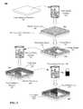
- FIG. 3is an illustrated process flow 300 depicting the non-deleterious creation of a continuous conductive circuit 360 upon a non-conductive substrate in accordance with embodiments of the inventive arrangements disclosed herein.
- FIG. 3Aillustrates the end state of the creation of a continuous conductive circuit upon the surface of a non-conductive substrate using the described non-deleterious process.
- the present inventiondiscloses a non-deleterious process that creates continuous conductive circuits upon the surface of a non-conductive substrate.
- a metallic base layercan be applied to one or more surfaces of the non-conductive substrate.
- a circuit patterncan be formed in the metallic base layer by removing the metallic base layer around the elements of the circuit pattern.
- a first metal layercan then be added to the metallic base layer.
- a second metal layer of an electrically conductive metalcan be added upon the first metal layer of the circuit pattern.
- FIG. 1is a flow chart of a method 100 providing a high-level overview of a non-deleterious process for creating continuous conductive circuits upon the surface of a non-conductive substrate in accordance with embodiments of the inventive arrangements disclosed herein.
- non-conductive substratecan be used to refer to a variety of materials that do not conduct any or conduct only a negligible amount of electricity.
- non-conductive substratesthat can be used in the process described herein can include, but are not limited to, high-molecular polymers, glass, ceramics, wood, fabric, stainless steel, and the like.
- non-deleteriouscan be used to indicate that the described process does not cause damage to or impair the integrity of the non-conductive substrate. That is, a continuous conductive circuit created using the described process can exist upon the surface of the non-conductive substrate without compromising the properties and/or original shape of the non-conductive substrate.
- Method 100can begin in step 105 where a metallic base layer can be applied to the surface or surfaces of the non-conductive substrate.
- Metals used to create the metallic base layercan include, but are not limited to, palladium, rhodium, platinum, iridium, osmium, gold, nickel, iron, and combinations thereof.
- a circuit patterncan then be formed within the metallic base layer in step 110 .
- a first metal layercan be added on top of the metallic base layer using a chemical plating process.
- a second metal layercan be added on top of the first metal layer using an electroplating process in step 120 , creating a continuous conductive circuit upon the surface or surfaces of the non-conductive substrate.
- the non-conductive substrate and/or continuous conductive circuitcan be further utilized in an electronics fabrication process (i.e., electronic components can be connected to the created continuous conductive circuit and/or the non-conductive substrate can be installed within a device).
- FIG. 2is a flow chart of a method 200 describing the non-deleterious process for creating continuous conductive circuits upon the surface of a non-conductive substrate in a finer detail in accordance with embodiments of the inventive arrangements disclosed herein.
- Method 200can represent a more specific embodiment of method 100 .
- Method 200can begin in step 205 where a prepared non-conductive substrate can be placed in an active metal solution. Preparation of the non-conductive substrate can include actions such as cleaning, degreasing, etching, and so on, as required for the specific implementation of the non-deleterious process and/or type of non-conductive substrate being used. After formation of a metallic base layer of the active metal upon the surface or surfaces of the non-conductive substrate, the non-conductive substrate can be removed from the active metal solution in step 210 .
- Performance of step 210can be based upon quantitative parameters like time in the solution and/or thickness of the active metal layer. These parameters can vary based upon the type of non-conductive substrate, application of continuous conductive circuit, and/or the specifics of the metallization process (e.g., molarity, specific active metal used).
- portions of the metallic base layercan be removed to realize a circuit pattern in the metallic base layer.
- the removal of the metallic base layer to realize the circuit patterncan separate circuit elements from the metallic base layer on the remainder of the non-conductive substrate.
- the region of the surface or surfaces of the non-conductive substrate in which the circuit pattern has been realizedcan be referred to as the plating region; the remainder of the non-conductive substrate surface or surfaces can be referred to as the non-plating region.
- preparation of the non-conductive substrate of step 205can include applying a substance on a portion of the non-conductive substrate that prevents or inhibits to a degree a bonding of the metallic base layer when the non-conductive substrate is placed in the active metal solution.
- This bonding inhibitorcan make removal of portions of the metallic base layer to create the plating region (of step 215 ) easier than would be otherwise possible.
- the patterned non-conductive substratecan then be placed into a chemical plating solution in step 220 .
- the non-conductive substratecan be removed from the chemical plating solution after the formation of a first metal layer, composed of the metal contained in the chemical plating solution, upon the metallic base layer. Areas of the non-conductive substrate exposed by the removal of the metallic base layer in step 215 can be unaffected by the chemical plating solution.
- the plating regioncan then be prepared (e.g., rinsed, dried, electrodes attached, etc.) for an electroplating process in step 230 .
- a second metal layercan be electroplated upon the first metal layer of the plating region.
- the electroplating processis only performed upon the plating region and the plating region is conductively separated from the non-plating region; hence, the second metal layer cannot form upon the first metal layer of the non-plating region.
- the first metal layer and the metallic base layercan be removed from the surface or surfaces of the non-conductive substrate in the non-plating region.
- FIG. 3is an illustrated process flow 300 depicting the non-deleterious creation of a continuous conductive circuit 380 upon a non-conductive substrate 305 in accordance with embodiments of the inventive arrangements disclosed herein.
- Process flow 300can represent a specific embodiment of methods 100 and/or 200 .
- Process flow 300can begin with a non-conductive substrate 305 that the surface or surfaces upon which the conductive circuit 380 is to be formed have already been prepared for metallization. It should be emphasized that the surface or surfaces of the non-conductive substrate 305 need not be limited to a planar silhouette. That is, the described process can create a conductive circuit 380 upon a non-conductive substrate 305 where the receiving surface includes concavity and/or convexity.
- this processcan create conductive circuits 380 upon an external (convex) or internal (concave) surface of a spherical or cylindrical object.
- the surfacecan have minor convexities and/or concavities like waves or ripples.
- the described processcan broaden the type of non-conductive substrate 305 topographies, in addition to shapes, that can be used as the basis for conductive circuits 380 .
- the described processcan allow the use of non-conductive substrates 305 whose surface imperfections can be considered unacceptable for conventional techniques and/or reduce the need for steps to improve surface flatness like chemical-mechanical planarization (CMP). That is, using the process described herein, no surface flatness improvements following by a photochemical machining (PCM) technique are necessary.
- CMPchemical-mechanical planarization
- the non-conductive substrate 305can be a piece of polycarbonate.
- the non-conductive substrate 305can be placed in an active metal solution 310 , such as a palladium solution having a molarity of 10-70 ppm.
- intermediary 315can have a metallic base layer 320 , indicated in light grey, upon the surface of the non-conductive substrate 305 , formed from the active metal supplied by the active metal solution 310 .
- the specific thickness of the active metal layer 320can vary based upon the type of active metal, the type of non-conductive substrate 305 , the type of conductive circuit 380 being formed, as well as other process-specific variables.
- the metallic base layer 320can be formed on the entirety of the surface area presented by the non-conductive substrate 305 , and that the layering shown in process flow 300 can represent a cut-away view so as to emphasize layer distinctions. That is, if all surfaces of the plate-shaped non-conductive substrate 305 are exposed when placed in the active metal solution 310 , then the resultant intermediary 315 would have a metallic base layer 320 covering the entirety of the non-conductive substrate 305 , and not just the “top” layer, as shown in this example.
- a circuit pattern 330can be realized in the metallic base layer 320 , resulting in intermediary 325 . Realization of the circuit pattern 330 can involve the removal of the metallic base layer 320 from the non-conductive substrate 305 around areas comprising the circuit pattern 330 .
- an yttrium aluminum garnet (YAG) lasercan be used to remove the metallic base layer 320 .
- the YAG lasercan provide a power of 4-10 W at a frequency of 5-30 kHz with a power density of 1-7%.
- the process to realize the circuit pattern 330 in the metallic base layer 320can physically separate the metallic base layer 320 into two separate regions.
- the plating region 335can include the circuit pattern 330 and any other auxiliary areas to be electroplated later in the process.
- the remainder of the metallic base layer 320 not included in the plating region 335can be referred to as the non-plating region 340 .
- the metallic base layer 320 of the non-plating region 340can be removed as well, leaving only the plating region 335 upon the surface of the non-conductive substrate 305 .
- Intermediary 325can then be placed in a chemical plating solution 345 to create intermediary 350 .
- the chemical plating solution 345can form a first metal layer 355 , indicated by the medium grey layer, upon the metallic base layer 320 , the light grey layer.
- an electroless copper plating processcan result in a first metal layer 355 of copper or an electroless nickel plating process can produce a nickel layer 355 .
- the first metal layer 355can be formed on the metallic base layer 320 in both the plating region 335 and the non-plating region 340 . While the first metal layer 355 , in essence, is only needed on the metallic base layer 320 of the circuit pattern 330 , creation of the first metal layer 355 in both regions 335 and 340 can be more cost-effective and time-saving than processing the non-conductive substrate 305 to inhibit the formation of the first metal layer 355 in the non-plating region 340 .
- coating the entirety of the metallic base layer 320 with the first metal layer 355 and later removing the first metal layer 355 from the non-plating region 340can be easier and more efficient than attempting to limit formation of the first metal layer 355 to the plating region 335 .
- An electroplating process 360can be used on the plating region 335 of intermediary 350 to produce intermediary 365 .
- the electrodes used in the electroplating process 360can be connected such that contact is made with only the plating region 335 . Therefore, the second metal layer 375 , indicated by the dark grey layer, can only form upon the first metal layer 355 contained within the plating region 335 .
- the non-conductive nature of the substrate 305can provide additional insulation and limit the electroplating process 360 to only the plating region 335 .
- Intermediary 365can then be used as an input medium for other electronic circuit processes.
- the first metal layer 355 and metallic base layer 320can be removed from intermediary 365 to produce the end state 375 shown in FIG. 3A .
- End state 375can include the conductive circuit 380 formed to the surface of the non-conductive substrate 305 .
- the conductive circuit 380can include the metallic base layer 320 that binds the first and second metal layers 355 and 370 to the non-conductive substrate 305 .
- Process flow 300can create the conductive circuit 380 without breaking the surface of the non-conductive substrate 305 , unlike other conventional formation techniques that embed one or more layers of the conductive circuit 380 within the non-conductive substrate 305 . This can keep the integrity of the non-conductive substrate 305 intact.
- the typical fabrication process for an integrated circuitcan involve specialized substrates (i.e., doped silicon wafers) and multiple lithographic, etching, and/or deposition steps to form the conductive circuit 380 .
- ICintegrated circuit
- substratesi.e., doped silicon wafers
- lithographic, etching, and/or deposition stepsto form the conductive circuit 380 .
- Implementing a single design change to this type of processcan result in reworking and/or changing the each mask that comprises the circuit pattern 330 , not to mention reconfiguring the machinery to work with the new/changed masks.
- circuit pattern 330is applied to the surface of the non-conductive substrate 305 as a single structure, a change to the design can be realized within this process by simply adjusting the process to the new circuit pattern 330 .
- the realization of the circuit pattern 330 within the metallic base layer 320can be altered to utilize the new circuit pattern 330 (i.e., the laser operator would follow the new circuit pattern 330 ).
- the new circuit pattern 330may also require a change in the placement of the electrodes during the electroplating process 360 . These process changes can be considered relatively minor when compared to those encountered in conventional conductive circuit 380 formation processes.
Landscapes
- Engineering & Computer Science (AREA)
- Chemical & Material Sciences (AREA)
- Chemical Kinetics & Catalysis (AREA)
- Microelectronics & Electronic Packaging (AREA)
- Materials Engineering (AREA)
- Electrochemistry (AREA)
- Metallurgy (AREA)
- Organic Chemistry (AREA)
- Manufacturing & Machinery (AREA)
- Physics & Mathematics (AREA)
- Condensed Matter Physics & Semiconductors (AREA)
- General Physics & Mathematics (AREA)
- Computer Hardware Design (AREA)
- Power Engineering (AREA)
- Manufacturing Of Printed Wiring (AREA)
Abstract
Description
Claims (9)
Priority Applications (22)
| Application Number | Priority Date | Filing Date | Title |
|---|---|---|---|
| US13/035,531US8621749B2 (en) | 2010-03-12 | 2011-02-25 | Non-deleterious technique for creating continuous conductive circuits |
| US13/285,219US8692790B2 (en) | 2011-02-25 | 2011-10-31 | Capacitive touch sensitive housing and method for making the same |
| TW101101448ATWI558293B (en) | 2011-02-25 | 2012-01-13 | A touch case and its manufacturing method |
| CN201210037238.2ACN102693054B (en) | 2011-02-25 | 2012-02-17 | Touch case and manufacturing method thereof |
| JP2013555533AJP5850954B2 (en) | 2011-02-25 | 2012-02-22 | Harmless technique for making continuous conductive circuits on the surface of non-conductive substrates |
| KR1020137022404AKR20130126977A (en) | 2011-02-25 | 2012-02-22 | A non-deleterious technique for creating continuous conductive circuits upon the surfaces of a non-conductive substrate |
| CN201610785889.8ACN106211611A (en) | 2011-02-25 | 2012-02-22 | Method for establishing continuous conductive circuit on surface of non-conductive substrate and conductive circuit |
| GB201316916AGB2502753B (en) | 2011-02-25 | 2012-02-22 | A non-deleterious technique for creating continuous conductive circuits upon the surfaces of a non-conductive substrate |
| PCT/US2012/026182WO2012116107A1 (en) | 2011-02-25 | 2012-02-22 | A non-deleterious technique for creating continuous conductive circuits upon the surfaces of a non-conductive substrate |
| CN201280010318.7ACN103477725B (en) | 2011-02-25 | 2012-02-22 | Harmless technology for establishing continuous conductive circuit on surface of non-conductive substrate |
| KR1020157014872AKR20150067403A (en) | 2011-02-25 | 2012-02-22 | A non-deleterious technique for creating continuous conductive circuits upon the surfaces of a non-conductive substrate |
| DE112012000993.2TDE112012000993B4 (en) | 2011-02-25 | 2012-02-22 | Harmless process for the production of continuous conductive strip conductors on the surfaces of a non-conductive substrate |
| TW104101431ATWI604766B (en) | 2011-02-25 | 2012-02-23 | A non-deleterious technique for creating continuous conductive circuits upon the surfaces of a non-conductive substrate |
| TW101105960ATWI475936B (en) | 2011-02-25 | 2012-02-23 | A non-deleterious technique for creating continuous conductive circuits upon the surfaces of a non-conductive substrate |
| DE102012003712.0ADE102012003712B4 (en) | 2011-02-25 | 2012-02-24 | Capacitive touch-sensitive housing and method for its manufacture |
| US13/547,494US20120273261A1 (en) | 2010-10-20 | 2012-07-12 | Circuit substrate having a circuit pattern and method for making the same |
| US14/134,046US9420699B2 (en) | 2010-03-12 | 2013-12-19 | Non-deleterious technique for creating continuous conductive circuits upon the surfaces of a non-conductive substrate |
| US14/149,457US9295162B2 (en) | 2010-03-12 | 2014-01-07 | Non-deleterious technique for creating continuous conductive circuits upon the surfaces of a non-conductive substrate |
| US14/196,107US8952919B2 (en) | 2011-02-25 | 2014-03-04 | Capacitive touch sensitive housing and method for making the same |
| US14/584,355US9678532B2 (en) | 2010-03-12 | 2014-12-29 | Capacitive touch sensitive housing and method for making the same |
| US14/933,616US9474161B2 (en) | 2010-03-12 | 2015-11-05 | Circuit substrate having a circuit pattern and method for making the same |
| US15/618,870US9933811B2 (en) | 2010-03-12 | 2017-06-09 | Capacitive touch sensitive housing and method for making the same |
Applications Claiming Priority (2)
| Application Number | Priority Date | Filing Date | Title |
|---|---|---|---|
| US31336710P | 2010-03-12 | 2010-03-12 | |
| US13/035,531US8621749B2 (en) | 2010-03-12 | 2011-02-25 | Non-deleterious technique for creating continuous conductive circuits |
Related Child Applications (4)
| Application Number | Title | Priority Date | Filing Date |
|---|---|---|---|
| US13/285,219Continuation-In-PartUS8692790B2 (en) | 2010-03-12 | 2011-10-31 | Capacitive touch sensitive housing and method for making the same |
| US13/547,494Continuation-In-PartUS20120273261A1 (en) | 2010-03-12 | 2012-07-12 | Circuit substrate having a circuit pattern and method for making the same |
| US14/134,046DivisionUS9420699B2 (en) | 2010-03-12 | 2013-12-19 | Non-deleterious technique for creating continuous conductive circuits upon the surfaces of a non-conductive substrate |
| US14/149,457ContinuationUS9295162B2 (en) | 2010-03-12 | 2014-01-07 | Non-deleterious technique for creating continuous conductive circuits upon the surfaces of a non-conductive substrate |
Publications (2)
| Publication Number | Publication Date |
|---|---|
| US20110278050A1 US20110278050A1 (en) | 2011-11-17 |
| US8621749B2true US8621749B2 (en) | 2014-01-07 |
Family
ID=44910752
Family Applications (3)
| Application Number | Title | Priority Date | Filing Date |
|---|---|---|---|
| US13/035,531Active2032-02-02US8621749B2 (en) | 2010-03-12 | 2011-02-25 | Non-deleterious technique for creating continuous conductive circuits |
| US14/134,046ActiveUS9420699B2 (en) | 2010-03-12 | 2013-12-19 | Non-deleterious technique for creating continuous conductive circuits upon the surfaces of a non-conductive substrate |
| US14/149,457Active2031-06-11US9295162B2 (en) | 2010-03-12 | 2014-01-07 | Non-deleterious technique for creating continuous conductive circuits upon the surfaces of a non-conductive substrate |
Family Applications After (2)
| Application Number | Title | Priority Date | Filing Date |
|---|---|---|---|
| US14/134,046ActiveUS9420699B2 (en) | 2010-03-12 | 2013-12-19 | Non-deleterious technique for creating continuous conductive circuits upon the surfaces of a non-conductive substrate |
| US14/149,457Active2031-06-11US9295162B2 (en) | 2010-03-12 | 2014-01-07 | Non-deleterious technique for creating continuous conductive circuits upon the surfaces of a non-conductive substrate |
Country Status (8)
| Country | Link |
|---|---|
| US (3) | US8621749B2 (en) |
| JP (1) | JP5850954B2 (en) |
| KR (2) | KR20150067403A (en) |
| CN (2) | CN106211611A (en) |
| DE (1) | DE112012000993B4 (en) |
| GB (1) | GB2502753B (en) |
| TW (2) | TWI475936B (en) |
| WO (1) | WO2012116107A1 (en) |
Cited By (4)
| Publication number | Priority date | Publication date | Assignee | Title |
|---|---|---|---|---|
| US9295162B2 (en) | 2010-03-12 | 2016-03-22 | Taiwan Green Point Enterprises Co., Ltd. | Non-deleterious technique for creating continuous conductive circuits upon the surfaces of a non-conductive substrate |
| US20160186327A1 (en)* | 2014-12-24 | 2016-06-30 | Taiwan Green Point Enterprises Co., Ltd. | Method for forming a circuit pattern on a substrate |
| US9474161B2 (en) | 2010-03-12 | 2016-10-18 | Taiwan Green Point Enterprises Co., Ltd. | Circuit substrate having a circuit pattern and method for making the same |
| US9678532B2 (en) | 2010-03-12 | 2017-06-13 | Taiwan Green Point Enterprises Co., Ltd. | Capacitive touch sensitive housing and method for making the same |
Families Citing this family (9)
| Publication number | Priority date | Publication date | Assignee | Title |
|---|---|---|---|---|
| US8692790B2 (en) | 2011-02-25 | 2014-04-08 | Taiwan Green Point Enterprises Co., Ltd. | Capacitive touch sensitive housing and method for making the same |
| TW201322835A (en)* | 2011-11-28 | 2013-06-01 | Taiwan Green Point Entpr Co | Fabricating a conductive trace structure and substrate having the structure |
| CN104221135B (en) | 2012-03-29 | 2017-10-24 | 绿点高新科技股份有限公司 | Double-sided circuit board and its preparation method |
| TWI531688B (en)* | 2013-09-16 | 2016-05-01 | Taiwan Green Point Entpr Co | Coating thickness uniform plating method |
| TW201614345A (en)* | 2014-10-15 | 2016-04-16 | Taiwan Green Point Entpr Co | A method for manufacturing a light emitting assembly, the light emitting assembly and a backlight module comprising the light emitting assembly |
| JP6265163B2 (en)* | 2015-04-02 | 2018-01-24 | トヨタ自動車株式会社 | Wiring pattern forming method and wiring pattern forming etching processing apparatus |
| TWI580084B (en)* | 2015-12-31 | 2017-04-21 | 綠點高新科技股份有限公司 | Light-emitting component and manufacturing method thereof |
| CN119300252A (en) | 2017-06-15 | 2025-01-10 | 捷普有限公司 | Systems, apparatus and methods for utilizing surface mount technology on metal substrates |
| EP3846597A4 (en)* | 2018-08-28 | 2022-05-18 | Kyocera Corporation | Wiring board and electronic device |
Citations (4)
| Publication number | Priority date | Publication date | Assignee | Title |
|---|---|---|---|---|
| US3781596A (en)* | 1972-07-07 | 1973-12-25 | R Galli | Semiconductor chip carriers and strips thereof |
| US4790912A (en)* | 1985-06-06 | 1988-12-13 | Techno-Instruments Investments Ltd. | Selective plating process for the electrolytic coating of circuit boards without an electroless metal coating |
| US4946563A (en)* | 1988-12-12 | 1990-08-07 | General Electric Company | Process for manufacturing a selective plated board for surface mount components |
| US6515233B1 (en)* | 2000-06-30 | 2003-02-04 | Daniel P. Labzentis | Method of producing flex circuit with selectively plated gold |
Family Cites Families (89)
| Publication number | Priority date | Publication date | Assignee | Title |
|---|---|---|---|---|
| US4066804A (en) | 1969-11-26 | 1978-01-03 | Imperial Chemical Industries Limited | Metal deposition process |
| US3853589A (en) | 1970-11-09 | 1974-12-10 | Ici Ltd | Metal deposition process |
| US3754939A (en) | 1972-05-23 | 1973-08-28 | Us Army | Electroless deposition of palladium alloys |
| DE2418654A1 (en) | 1974-04-18 | 1975-11-06 | Langbein Pfanhauser Werke Ag | PROCESS FOR ELECTRONIC SURFACE METALIZATION OF PLASTIC OBJECTS AND A SUITABLE ACTIVATING BATH TO PERFORM THE PROCESS |
| JPS608592B2 (en)* | 1977-11-07 | 1985-03-04 | 旭化成株式会社 | Connector manufacturing method |
| US4264646A (en) | 1979-03-12 | 1981-04-28 | Xerox Corporation | Selectively electrolessly depositing a metal pattern on the surface of a laminar film |
| JPS616892A (en)* | 1984-06-20 | 1986-01-13 | キヤノン株式会社 | How to make printed circuits |
| US4574095A (en) | 1984-11-19 | 1986-03-04 | International Business Machines Corporation | Selective deposition of copper |
| US4865873A (en) | 1986-09-15 | 1989-09-12 | General Electric Company | Electroless deposition employing laser-patterned masking layer |
| US4882200A (en) | 1987-05-21 | 1989-11-21 | General Electric Company | Method for photopatterning metallization via UV-laser ablation of the activator |
| DE68922118T2 (en)* | 1988-01-25 | 1995-10-12 | Toshiba Kawasaki Kk | Circuit board. |
| US4877644A (en) | 1988-04-12 | 1989-10-31 | Amp Incorporated | Selective plating by laser ablation |
| US4898648A (en)* | 1988-11-15 | 1990-02-06 | Pacific Bell | Method for providing a strengthened conductive circuit pattern |
| US4988412A (en)* | 1988-12-27 | 1991-01-29 | General Electric Company | Selective electrolytic desposition on conductive and non-conductive substrates |
| US5084299A (en) | 1989-08-10 | 1992-01-28 | Microelectronics And Computer Technology Corporation | Method for patterning electroless plated metal on a polymer substrate |
| US4925522A (en)* | 1989-08-21 | 1990-05-15 | Gte Products Corporation | Printed circuit assembly with contact dot |
| US5086966A (en) | 1990-11-05 | 1992-02-11 | Motorola Inc. | Palladium-coated solder ball |
| JP2948366B2 (en) | 1991-09-05 | 1999-09-13 | 塚田理研工業株式会社 | Partial plating method for plastic moldings |
| EP0530564A1 (en) | 1991-09-05 | 1993-03-10 | Siemens Aktiengesellschaft | Method for producing circuit boards |
| JPH05109728A (en) | 1991-10-16 | 1993-04-30 | Nec Corp | Manufacture of semiconductor device |
| DE59106557D1 (en) | 1991-11-21 | 1995-10-26 | Siemens Ag | Process for the production of printed circuit boards. |
| JP3153682B2 (en) | 1993-08-26 | 2001-04-09 | 松下電工株式会社 | Circuit board manufacturing method |
| BE1007610A3 (en)* | 1993-10-11 | 1995-08-22 | Philips Electronics Nv | METHOD FOR ENERGIZE APPLYING A PATTERN ON METAL an electrically insulating substrate. |
| US6325910B1 (en) | 1994-04-08 | 2001-12-04 | Atotch Deutschland Gmbh | Palladium colloid solution and its utilization |
| US5525204A (en) | 1994-09-29 | 1996-06-11 | Motorola, Inc. | Method for fabricating a printed circuit for DCA semiconductor chips |
| JPH09107170A (en)* | 1995-10-13 | 1997-04-22 | Toppan Printing Co Ltd | Manufacturing method of printed wiring board |
| JPH1018080A (en)* | 1996-06-27 | 1998-01-20 | Totoku Electric Co Ltd | Method for forming metal conductive layer on fluororesin surface |
| US5924364A (en) | 1997-01-17 | 1999-07-20 | Agfa-Gevaert N.V. | Laser-imagable recording material and printing plate produced therefrom for waterless offset printing |
| JPH10209609A (en)* | 1997-01-17 | 1998-08-07 | Totoku Electric Co Ltd | Method of manufacturing flexible printed circuit and flexible printed circuit obtained by the method |
| JPH10209607A (en)* | 1997-01-23 | 1998-08-07 | Matsushita Electric Works Ltd | Manufacture of circuit board |
| JP3458648B2 (en)* | 1997-03-17 | 2003-10-20 | 松下電工株式会社 | Circuit board |
| CN1155304C (en) | 1997-04-15 | 2004-06-23 | 揖斐电株式会社 | Adhesive for electroless plating and printed wiring board |
| DE19731346C2 (en) | 1997-06-06 | 2003-09-25 | Lpkf Laser & Electronics Ag | Conductor structures and a method for their production |
| JPH1197824A (en) | 1997-09-22 | 1999-04-09 | Matsushita Electric Works Ltd | Manufacture of circuit board |
| US6291093B1 (en) | 1997-11-25 | 2001-09-18 | California Institute Of Technology | Fuel cell elements with improved water handling capacity |
| US6162365A (en)* | 1998-03-04 | 2000-12-19 | International Business Machines Corporation | Pd etch mask for copper circuitization |
| EP1091024A4 (en) | 1998-04-30 | 2006-03-22 | Ebara Corp | Method and device for plating substrate |
| US6188391B1 (en) | 1998-07-09 | 2001-02-13 | Synaptics, Inc. | Two-layer capacitive touchpad and method of making same |
| MY139405A (en) | 1998-09-28 | 2009-09-30 | Ibiden Co Ltd | Printed circuit board and method for its production |
| JP2000232269A (en) | 1999-02-10 | 2000-08-22 | Nec Toyama Ltd | Printed wiring board and manufacture thereof |
| US6359233B1 (en)* | 1999-10-26 | 2002-03-19 | Intel Corporation | Printed circuit board multipack structure having internal gold fingers and multipack and printed circuit board formed therefrom, and methods of manufacture thereof |
| US6242156B1 (en) | 2000-06-28 | 2001-06-05 | Gary Ganghui Teng | Lithographic plate having a conformal radiation-sensitive layer on a rough substrate |
| US6801438B1 (en) | 2000-10-24 | 2004-10-05 | Touch Future Technolocy Ltd. | Electrical circuit and method of formation |
| SG108820A1 (en) | 2001-02-23 | 2005-02-28 | Agency Science Tech & Res | Method and apparatus for forming a metallic feature on a substrate |
| KR20020071437A (en) | 2001-03-06 | 2002-09-12 | 유승균 | Plating method of metal film on the surface of polymer |
| DE10132092A1 (en) | 2001-07-05 | 2003-01-23 | Lpkf Laser & Electronics Ag | Track structures and processes for their manufacture |
| JP4208440B2 (en) | 2001-07-19 | 2009-01-14 | 富士フイルム株式会社 | Development processing method for lithographic printing plate precursor |
| KR20050026904A (en) | 2001-09-10 | 2005-03-16 | 마이크로브리지 테크놀로지스 인크. | Method for trimming resistors |
| KR100396787B1 (en)* | 2001-11-13 | 2003-09-02 | 엘지전자 주식회사 | Wire bonding pad structure of semiconductor package pcb |
| US20040149986A1 (en) | 2002-04-16 | 2004-08-05 | Dubowski Jan J. | Multilayer microstructures and laser based method for precision and reduced damage patterning of such structures |
| US7176897B2 (en) | 2002-05-17 | 2007-02-13 | 3M Innovative Properties Company | Correction of memory effect errors in force-based touch panel systems |
| US7361313B2 (en) | 2003-02-18 | 2008-04-22 | Intel Corporation | Methods for uniform metal impregnation into a nanoporous material |
| US7656393B2 (en) | 2005-03-04 | 2010-02-02 | Apple Inc. | Electronic device having display and surrounding touch sensitive bezel for user interface and control |
| ATE350884T1 (en) | 2002-07-18 | 2007-01-15 | Festo Ag & Co | INJECTION-MOLDED CONDUCTOR SUPPORT AND METHOD FOR THE PRODUCTION THEREOF |
| US20050112432A1 (en)* | 2002-08-27 | 2005-05-26 | Jonah Erlebacher | Method of plating metal leafs and metal membranes |
| US6773760B1 (en) | 2003-04-28 | 2004-08-10 | Yuh Sung | Method for metallizing surfaces of substrates |
| JP2005050965A (en)* | 2003-07-31 | 2005-02-24 | Ngk Spark Plug Co Ltd | Wiring board and its manufacturing method |
| WO2005054120A2 (en) | 2003-12-05 | 2005-06-16 | Idaho Research Foundation, Inc. | Polymer-supported metal nanoparticles and method for their manufacture and use |
| US7145238B1 (en)* | 2004-05-05 | 2006-12-05 | Amkor Technology, Inc. | Semiconductor package and substrate having multi-level vias |
| US7291380B2 (en) | 2004-07-09 | 2007-11-06 | Hewlett-Packard Development Company, L.P. | Laser enhanced plating for forming wiring patterns |
| US7094669B2 (en) | 2004-08-03 | 2006-08-22 | Chartered Semiconductor Manufacturing Ltd | Structure and method of liner air gap formation |
| US7279407B2 (en) | 2004-09-02 | 2007-10-09 | Micron Technology, Inc. | Selective nickel plating of aluminum, copper, and tungsten structures |
| US7719522B2 (en) | 2004-09-24 | 2010-05-18 | Apple Inc. | Raw data track pad device and system |
| US7517791B2 (en) | 2004-11-30 | 2009-04-14 | Semiconductor Energy Laboratory Co., Ltd. | Method for manufacturing semiconductor device |
| US7237334B2 (en)* | 2005-08-18 | 2007-07-03 | Intel Corporation | Method of providing a printed circuit board using laser assisted metallization and patterning of a microelectronic substrate |
| US7630207B2 (en) | 2005-09-15 | 2009-12-08 | Fujifilm Corporation | Wiring board, method of manufacturing wiring board, and liquid ejection head |
| US7913644B2 (en) | 2005-09-30 | 2011-03-29 | Lam Research Corporation | Electroless deposition system |
| US20070148420A1 (en) | 2005-12-28 | 2007-06-28 | Intel Corporation | Method of making a substrate using laser assisted metallization and patterning with electroless plating without electrolytic plating |
| DE102006017630A1 (en) | 2006-04-12 | 2007-10-18 | Lpkf Laser & Electronics Ag | Method for producing a printed conductor structure and a printed conductor structure produced in this way |
| JP4903479B2 (en) | 2006-04-18 | 2012-03-28 | 富士フイルム株式会社 | Metal pattern forming method, metal pattern, and printed wiring board |
| US7779522B2 (en) | 2006-05-05 | 2010-08-24 | Fujifilm Dimatix, Inc. | Method for forming a MEMS |
| US20080001297A1 (en) | 2006-06-30 | 2008-01-03 | Stefanie Lotz | Laser patterning and conductive interconnect/materials forming techniques for fine line and space features |
| KR20090103949A (en)* | 2007-01-19 | 2009-10-01 | 바스프 에스이 | Method for the production of structured, electrically conductive surfaces |
| JP5286046B2 (en) | 2007-11-30 | 2013-09-11 | 株式会社半導体エネルギー研究所 | Method for manufacturing photoelectric conversion device |
| EP2124514A1 (en) | 2008-05-23 | 2009-11-25 | Nederlandse Centrale Organisatie Voor Toegepast Natuurwetenschappelijk Onderzoek TNO | Providing a plastic substrate with a metallic pattern |
| US7754601B2 (en) | 2008-06-03 | 2010-07-13 | Taiwan Semiconductor Manufacturing Co., Ltd. | Semiconductor interconnect air gap formation process |
| US9335868B2 (en) | 2008-07-31 | 2016-05-10 | Apple Inc. | Capacitive sensor behind black mask |
| US7956548B2 (en) | 2009-04-08 | 2011-06-07 | Kanghong Zhang | Electronic ballast protection |
| US20100258173A1 (en)* | 2009-04-13 | 2010-10-14 | Joseph Laia | Polishing a thin metallic substrate for a solar cell |
| US8436473B2 (en) | 2009-05-06 | 2013-05-07 | Taiwan Semiconductor Manufacturing Company, Ltd. | Integrated circuits including air gaps around interconnect structures, and fabrication methods thereof |
| CN201413834Y (en)* | 2009-05-18 | 2010-02-24 | 光宏精密股份有限公司 | Bearing structure of electronic element |
| JP4996653B2 (en)* | 2009-07-10 | 2012-08-08 | 三共化成株式会社 | Manufacturing method of molded circuit components |
| FR2954580B1 (en)* | 2009-12-22 | 2011-12-09 | Commissariat Energie Atomique | METHOD FOR PRODUCING A NON-PLAN MICROELECTRONIC COMPONENT |
| US20120273261A1 (en) | 2010-10-20 | 2012-11-01 | Taiwan Green Point Enterprises Co., Ltd. | Circuit substrate having a circuit pattern and method for making the same |
| US8952919B2 (en) | 2011-02-25 | 2015-02-10 | Taiwan Green Point Enterprises Co., Ltd. | Capacitive touch sensitive housing and method for making the same |
| US8692790B2 (en) | 2011-02-25 | 2014-04-08 | Taiwan Green Point Enterprises Co., Ltd. | Capacitive touch sensitive housing and method for making the same |
| US8621749B2 (en) | 2010-03-12 | 2014-01-07 | Taiwan Green Point Enterprises Co., Ltd | Non-deleterious technique for creating continuous conductive circuits |
| CN101873766B (en)* | 2010-06-02 | 2011-07-27 | 上海律图表面处理有限公司 | Method for manufacturing conductor track structure |
| US20120278050A1 (en) | 2011-04-29 | 2012-11-01 | Taiwan Semiconductor Manufacturing Company, Ltd. | Accelerated Generation of Circuit Parameter Distribution Using Monte Carlo Simulation |
- 2011
- 2011-02-25USUS13/035,531patent/US8621749B2/enactiveActive
- 2012
- 2012-02-22KRKR1020157014872Apatent/KR20150067403A/ennot_activeCeased
- 2012-02-22WOPCT/US2012/026182patent/WO2012116107A1/enactiveApplication Filing
- 2012-02-22CNCN201610785889.8Apatent/CN106211611A/enactivePending
- 2012-02-22JPJP2013555533Apatent/JP5850954B2/enactiveActive
- 2012-02-22GBGB201316916Apatent/GB2502753B/enactiveActive
- 2012-02-22DEDE112012000993.2Tpatent/DE112012000993B4/enactiveActive
- 2012-02-22KRKR1020137022404Apatent/KR20130126977A/ennot_activeCeased
- 2012-02-22CNCN201280010318.7Apatent/CN103477725B/enactiveActive
- 2012-02-23TWTW101105960Apatent/TWI475936B/enactive
- 2012-02-23TWTW104101431Apatent/TWI604766B/enactive
- 2013
- 2013-12-19USUS14/134,046patent/US9420699B2/enactiveActive
- 2014
- 2014-01-07USUS14/149,457patent/US9295162B2/enactiveActive
Patent Citations (4)
| Publication number | Priority date | Publication date | Assignee | Title |
|---|---|---|---|---|
| US3781596A (en)* | 1972-07-07 | 1973-12-25 | R Galli | Semiconductor chip carriers and strips thereof |
| US4790912A (en)* | 1985-06-06 | 1988-12-13 | Techno-Instruments Investments Ltd. | Selective plating process for the electrolytic coating of circuit boards without an electroless metal coating |
| US4946563A (en)* | 1988-12-12 | 1990-08-07 | General Electric Company | Process for manufacturing a selective plated board for surface mount components |
| US6515233B1 (en)* | 2000-06-30 | 2003-02-04 | Daniel P. Labzentis | Method of producing flex circuit with selectively plated gold |
Cited By (6)
| Publication number | Priority date | Publication date | Assignee | Title |
|---|---|---|---|---|
| US9295162B2 (en) | 2010-03-12 | 2016-03-22 | Taiwan Green Point Enterprises Co., Ltd. | Non-deleterious technique for creating continuous conductive circuits upon the surfaces of a non-conductive substrate |
| US9420699B2 (en) | 2010-03-12 | 2016-08-16 | Taiwan Green Point Enterprises Co., Ltd. | Non-deleterious technique for creating continuous conductive circuits upon the surfaces of a non-conductive substrate |
| US9474161B2 (en) | 2010-03-12 | 2016-10-18 | Taiwan Green Point Enterprises Co., Ltd. | Circuit substrate having a circuit pattern and method for making the same |
| US9678532B2 (en) | 2010-03-12 | 2017-06-13 | Taiwan Green Point Enterprises Co., Ltd. | Capacitive touch sensitive housing and method for making the same |
| US9933811B2 (en) | 2010-03-12 | 2018-04-03 | Taiwan Green Point Enterprises Co., Ltd. | Capacitive touch sensitive housing and method for making the same |
| US20160186327A1 (en)* | 2014-12-24 | 2016-06-30 | Taiwan Green Point Enterprises Co., Ltd. | Method for forming a circuit pattern on a substrate |
Also Published As
| Publication number | Publication date |
|---|---|
| WO2012116107A1 (en) | 2012-08-30 |
| US20110278050A1 (en) | 2011-11-17 |
| CN103477725B (en) | 2016-10-12 |
| TW201517723A (en) | 2015-05-01 |
| TW201247065A (en) | 2012-11-16 |
| CN106211611A (en) | 2016-12-07 |
| KR20130126977A (en) | 2013-11-21 |
| US9420699B2 (en) | 2016-08-16 |
| JP2014506737A (en) | 2014-03-17 |
| DE112012000993T5 (en) | 2014-01-16 |
| DE112012000993B4 (en) | 2022-01-05 |
| TWI604766B (en) | 2017-11-01 |
| TWI475936B (en) | 2015-03-01 |
| JP5850954B2 (en) | 2016-02-03 |
| GB201316916D0 (en) | 2013-11-06 |
| GB2502753A (en) | 2013-12-04 |
| US9295162B2 (en) | 2016-03-22 |
| GB2502753B (en) | 2015-04-22 |
| CN103477725A (en) | 2013-12-25 |
| US20140102775A1 (en) | 2014-04-17 |
| US20140116885A1 (en) | 2014-05-01 |
| KR20150067403A (en) | 2015-06-17 |
Similar Documents
| Publication | Publication Date | Title |
|---|---|---|
| US8621749B2 (en) | Non-deleterious technique for creating continuous conductive circuits | |
| CN1088321C (en) | Method of making circuitized substrate using two different metallization processes | |
| WO2003023848A3 (en) | Apparatus and method of surface treatment for electrolytic and electroless plating of metals in integrated circuit manufacturing | |
| KR20070065241A (en) | Manufacturing method of IC embedded board | |
| US7562447B2 (en) | Method of manufacturing printed circuit board for fine circuit formation | |
| JP7118426B2 (en) | Printed Circuit Surface Finishes, Methods of Use, and Assemblies Made Therefrom | |
| US20110123930A1 (en) | Ceramic substrate preparation process | |
| TW201347626A (en) | Printed circuit board and method of manufacturing the same | |
| CN103813657B (en) | The printed circuit board manufacturing method | |
| US6544392B1 (en) | Apparatus for manufacturing pcb's | |
| JP7525612B2 (en) | Circuit board and manufacturing method thereof | |
| CN115003060A (en) | Etching process for preventing plated copper of PTH hole from being too thin | |
| KR20150041357A (en) | Electroless plating method for plasma components | |
| JP4639975B2 (en) | Manufacturing method of three-dimensional circuit board | |
| KR100901017B1 (en) | Metal pattern formation method of substrate | |
| KR101427388B1 (en) | Reinforcing Substrate for Supporting Printed Circuit Board and Method for Processing for the Same | |
| KR102201500B1 (en) | Ceramic housing and plating method of ceramic material | |
| Hsieh et al. | Microstructure of Weak-Micro-Via and its Failure Prevention | |
| CN114760777A (en) | Selective composite electrogilding substrate and manufacturing process thereof | |
| CN118921886A (en) | Method for manufacturing pad plate ultra-fine circuit by adopting pre-buried transfer copper pad | |
| JP2008135570A (en) | Method of manufacturing wiring board | |
| KR20060001307A (en) | Copper Plating Method Of Semiconductor Devices |
Legal Events
| Date | Code | Title | Description |
|---|---|---|---|
| AS | Assignment | Owner name:JABIL CIRCUIT, INC., FLORIDA Free format text:ASSIGNMENT OF ASSIGNORS INTEREST;ASSIGNORS:YI, SHEN-HENG;LIAO, PEN YI;SIGNING DATES FROM 20110218 TO 20110222;REEL/FRAME:025867/0069 | |
| AS | Assignment | Owner name:JABIL CIRCUIT, INC., FLORIDA Free format text:ASSIGNMENT OF ASSIGNORS INTEREST;ASSIGNORS:YI, SHENG-HUNG;LIAO, PEN-YI;REEL/FRAME:026676/0193 Effective date:20110615 | |
| AS | Assignment | Owner name:TAIWAN GREEN POINT ENTERPRISES CO., LTD., TAIWAN Free format text:ASSIGNMENT OF ASSIGNORS INTEREST;ASSIGNOR:JABIL CIRCUIT, INC.;REEL/FRAME:030943/0285 Effective date:20130802 | |
| FEPP | Fee payment procedure | Free format text:PAYOR NUMBER ASSIGNED (ORIGINAL EVENT CODE: ASPN); ENTITY STATUS OF PATENT OWNER: LARGE ENTITY | |
| STCF | Information on status: patent grant | Free format text:PATENTED CASE | |
| AS | Assignment | Owner name:TAIWAN GREEN POINT ENTERPRISES CO., LTD., TAIWAN Free format text:CHANGE OF ASSIGNEE'S ADDRESS;ASSIGNOR:TAIWAN GREEN POINT ENTERPRISES CO., LTD.;REEL/FRAME:035334/0361 Effective date:20150323 | |
| FPAY | Fee payment | Year of fee payment:4 | |
| MAFP | Maintenance fee payment | Free format text:PAYMENT OF MAINTENANCE FEE, 8TH YEAR, LARGE ENTITY (ORIGINAL EVENT CODE: M1552); ENTITY STATUS OF PATENT OWNER: LARGE ENTITY Year of fee payment:8 | |
| MAFP | Maintenance fee payment | Free format text:PAYMENT OF MAINTENANCE FEE, 12TH YEAR, LARGE ENTITY (ORIGINAL EVENT CODE: M1553); ENTITY STATUS OF PATENT OWNER: LARGE ENTITY Year of fee payment:12 |