US8617945B2 - Stacking fault and twin blocking barrier for integrating III-V on Si - Google Patents
Stacking fault and twin blocking barrier for integrating III-V on SiDownload PDFInfo
- Publication number
- US8617945B2 US8617945B2US13/366,143US201213366143AUS8617945B2US 8617945 B2US8617945 B2US 8617945B2US 201213366143 AUS201213366143 AUS 201213366143AUS 8617945 B2US8617945 B2US 8617945B2
- Authority
- US
- United States
- Prior art keywords
- layer
- silicon substrate
- source
- gasb
- iii
- Prior art date
- Legal status (The legal status is an assumption and is not a legal conclusion. Google has not performed a legal analysis and makes no representation as to the accuracy of the status listed.)
- Expired - Fee Related
Links
- 230000004888barrier functionEffects0.000titleabstractdescription35
- 230000000903blocking effectEffects0.000titleabstractdescription3
- 239000000758substrateSubstances0.000claimsabstractdescription93
- XUIMIQQOPSSXEZ-UHFFFAOYSA-NSiliconChemical compound[Si]XUIMIQQOPSSXEZ-UHFFFAOYSA-N0.000claimsabstractdescription77
- 229910052710siliconInorganic materials0.000claimsabstractdescription77
- 239000010703siliconSubstances0.000claimsabstractdescription77
- 229910005542GaSbInorganic materials0.000claimsabstractdescription48
- 238000000034methodMethods0.000claimsabstractdescription34
- WPYVAWXEWQSOGY-UHFFFAOYSA-Nindium antimonideChemical compound[Sb]#[In]WPYVAWXEWQSOGY-UHFFFAOYSA-N0.000claimsabstractdescription25
- 230000006911nucleationEffects0.000claimsdescription32
- 238000010899nucleationMethods0.000claimsdescription32
- 239000004065semiconductorSubstances0.000claimsdescription31
- 238000004211migration-enhanced epitaxyMethods0.000claimsdescription16
- 238000000151depositionMethods0.000claimsdescription11
- 229910052787antimonyInorganic materials0.000claimsdescription5
- 150000001875compoundsChemical class0.000claimsdescription4
- 229910052733galliumInorganic materials0.000claimsdescription4
- 238000009416shutteringMethods0.000claims4
- 230000007547defectEffects0.000abstractdescription27
- 238000004519manufacturing processMethods0.000abstractdescription8
- 230000008018meltingEffects0.000abstractdescription6
- 238000002844meltingMethods0.000abstractdescription6
- 230000001902propagating effectEffects0.000abstractdescription2
- 239000010410layerSubstances0.000description203
- 239000000463materialSubstances0.000description34
- 239000010408filmSubstances0.000description24
- JBRZTFJDHDCESZ-UHFFFAOYSA-NAsGaChemical compound[As]#[Ga]JBRZTFJDHDCESZ-UHFFFAOYSA-N0.000description12
- 229910001218Gallium arsenideInorganic materials0.000description10
- 239000013078crystalSubstances0.000description8
- 230000008569processEffects0.000description8
- 230000015572biosynthetic processEffects0.000description6
- 230000001627detrimental effectEffects0.000description5
- RPQDHPTXJYYUPQ-UHFFFAOYSA-Nindium arsenideChemical compound[In]#[As]RPQDHPTXJYYUPQ-UHFFFAOYSA-N0.000description5
- 229910000530Gallium indium arsenideInorganic materials0.000description4
- KXNLCSXBJCPWGL-UHFFFAOYSA-N[Ga].[As].[In]Chemical compound[Ga].[As].[In]KXNLCSXBJCPWGL-UHFFFAOYSA-N0.000description4
- 230000008901benefitEffects0.000description4
- 238000001451molecular beam epitaxyMethods0.000description4
- KRKNYBCHXYNGOX-UHFFFAOYSA-Ncitric acidChemical compoundOC(=O)CC(O)(C(O)=O)CC(O)=OKRKNYBCHXYNGOX-UHFFFAOYSA-N0.000description3
- 229910000673Indium arsenideInorganic materials0.000description2
- AUCDRFABNLOFRE-UHFFFAOYSA-Nalumane;indiumChemical compound[AlH3].[In]AUCDRFABNLOFRE-UHFFFAOYSA-N0.000description2
- 229910052782aluminiumInorganic materials0.000description2
- XAGFODPZIPBFFR-UHFFFAOYSA-NaluminiumChemical compound[Al]XAGFODPZIPBFFR-UHFFFAOYSA-N0.000description2
- AJGDITRVXRPLBY-UHFFFAOYSA-Naluminum indiumChemical compound[Al].[In]AJGDITRVXRPLBY-UHFFFAOYSA-N0.000description2
- WATWJIUSRGPENY-UHFFFAOYSA-Nantimony atomChemical compound[Sb]WATWJIUSRGPENY-UHFFFAOYSA-N0.000description2
- 238000000231atomic layer depositionMethods0.000description2
- 239000000969carrierSubstances0.000description2
- 239000002800charge carrierSubstances0.000description2
- 238000010586diagramMethods0.000description2
- 230000004907fluxEffects0.000description2
- 238000002955isolationMethods0.000description2
- 230000005012migrationEffects0.000description2
- 238000013508migrationMethods0.000description2
- 230000003287optical effectEffects0.000description2
- 208000032750Device leakageDiseases0.000description1
- GYHNNYVSQQEPJS-UHFFFAOYSA-NGalliumChemical compound[Ga]GYHNNYVSQQEPJS-UHFFFAOYSA-N0.000description1
- LVQULNGDVIKLPK-UHFFFAOYSA-Naluminium antimonideChemical compound[Sb]#[Al]LVQULNGDVIKLPK-UHFFFAOYSA-N0.000description1
- 238000003491arrayMethods0.000description1
- 229910052785arsenicInorganic materials0.000description1
- RQNWIZPPADIBDY-UHFFFAOYSA-Narsenic atomChemical compound[As]RQNWIZPPADIBDY-UHFFFAOYSA-N0.000description1
- 230000008859changeEffects0.000description1
- 238000005229chemical vapour depositionMethods0.000description1
- 239000000470constituentSubstances0.000description1
- 238000005336crackingMethods0.000description1
- 238000005520cutting processMethods0.000description1
- 230000001419dependent effectEffects0.000description1
- 238000005137deposition processMethods0.000description1
- 238000005566electron beam evaporationMethods0.000description1
- 238000000313electron-beam-induced depositionMethods0.000description1
- 230000006870functionEffects0.000description1
- VTGARNNDLOTBET-UHFFFAOYSA-Ngallium antimonideChemical compound[Sb]#[Ga]VTGARNNDLOTBET-UHFFFAOYSA-N0.000description1
- 229910021478group 5 elementInorganic materials0.000description1
- 239000012535impuritySubstances0.000description1
- 230000010354integrationEffects0.000description1
- 238000001459lithographyMethods0.000description1
- 238000001465metallisationMethods0.000description1
- 238000004377microelectronicMethods0.000description1
- 230000005693optoelectronicsEffects0.000description1
- 150000002978peroxidesChemical class0.000description1
- 238000005036potential barrierMethods0.000description1
- 239000002243precursorSubstances0.000description1
- 238000002360preparation methodMethods0.000description1
- 230000000644propagated effectEffects0.000description1
- 238000005546reactive sputteringMethods0.000description1
- 230000009467reductionEffects0.000description1
- 239000002356single layerSubstances0.000description1
- 238000000638solvent extractionMethods0.000description1
- VEALVRVVWBQVSL-UHFFFAOYSA-Nstrontium titanateChemical compound[Sr+2].[O-][Ti]([O-])=OVEALVRVVWBQVSL-UHFFFAOYSA-N0.000description1
- 239000002344surface layerSubstances0.000description1
- 229910052714telluriumInorganic materials0.000description1
- PORWMNRCUJJQNO-UHFFFAOYSA-Ntellurium atomChemical compound[Te]PORWMNRCUJJQNO-UHFFFAOYSA-N0.000description1
- 238000007725thermal activationMethods0.000description1
- 239000010409thin filmSubstances0.000description1
- 238000012876topographyMethods0.000description1
- 210000003462veinAnatomy0.000description1
- 238000009736wettingMethods0.000description1
Images


Classifications
- H—ELECTRICITY
- H10—SEMICONDUCTOR DEVICES; ELECTRIC SOLID-STATE DEVICES NOT OTHERWISE PROVIDED FOR
- H10D—INORGANIC ELECTRIC SEMICONDUCTOR DEVICES
- H10D30/00—Field-effect transistors [FET]
- H10D30/40—FETs having zero-dimensional [0D], one-dimensional [1D] or two-dimensional [2D] charge carrier gas channels
- H10D30/47—FETs having zero-dimensional [0D], one-dimensional [1D] or two-dimensional [2D] charge carrier gas channels having 2D charge carrier gas channels, e.g. nanoribbon FETs or high electron mobility transistors [HEMT]
- H10D30/471—High electron mobility transistors [HEMT] or high hole mobility transistors [HHMT]
- H10D30/473—High electron mobility transistors [HEMT] or high hole mobility transistors [HHMT] having confinement of carriers by multiple heterojunctions, e.g. quantum well HEMT
- H10D30/4732—High electron mobility transistors [HEMT] or high hole mobility transistors [HHMT] having confinement of carriers by multiple heterojunctions, e.g. quantum well HEMT using Group III-V semiconductor material
- H10D30/4738—High electron mobility transistors [HEMT] or high hole mobility transistors [HHMT] having confinement of carriers by multiple heterojunctions, e.g. quantum well HEMT using Group III-V semiconductor material having multiple donor layers
- H—ELECTRICITY
- H01—ELECTRIC ELEMENTS
- H01L—SEMICONDUCTOR DEVICES NOT COVERED BY CLASS H10
- H01L21/00—Processes or apparatus adapted for the manufacture or treatment of semiconductor or solid state devices or of parts thereof
- H01L21/02—Manufacture or treatment of semiconductor devices or of parts thereof
- H01L21/02104—Forming layers
- H01L21/02365—Forming inorganic semiconducting materials on a substrate
- H01L21/02367—Substrates
- H01L21/0237—Materials
- H01L21/02373—Group 14 semiconducting materials
- H01L21/02381—Silicon, silicon germanium, germanium
- H—ELECTRICITY
- H01—ELECTRIC ELEMENTS
- H01L—SEMICONDUCTOR DEVICES NOT COVERED BY CLASS H10
- H01L21/00—Processes or apparatus adapted for the manufacture or treatment of semiconductor or solid state devices or of parts thereof
- H01L21/02—Manufacture or treatment of semiconductor devices or of parts thereof
- H01L21/02104—Forming layers
- H01L21/02365—Forming inorganic semiconducting materials on a substrate
- H01L21/02367—Substrates
- H01L21/02433—Crystal orientation
- H—ELECTRICITY
- H01—ELECTRIC ELEMENTS
- H01L—SEMICONDUCTOR DEVICES NOT COVERED BY CLASS H10
- H01L21/00—Processes or apparatus adapted for the manufacture or treatment of semiconductor or solid state devices or of parts thereof
- H01L21/02—Manufacture or treatment of semiconductor devices or of parts thereof
- H01L21/02104—Forming layers
- H01L21/02365—Forming inorganic semiconducting materials on a substrate
- H01L21/02436—Intermediate layers between substrates and deposited layers
- H01L21/02439—Materials
- H01L21/02455—Group 13/15 materials
- H01L21/02466—Antimonides
- H—ELECTRICITY
- H01—ELECTRIC ELEMENTS
- H01L—SEMICONDUCTOR DEVICES NOT COVERED BY CLASS H10
- H01L21/00—Processes or apparatus adapted for the manufacture or treatment of semiconductor or solid state devices or of parts thereof
- H01L21/02—Manufacture or treatment of semiconductor devices or of parts thereof
- H01L21/02104—Forming layers
- H01L21/02365—Forming inorganic semiconducting materials on a substrate
- H01L21/02518—Deposited layers
- H01L21/02521—Materials
- H01L21/02538—Group 13/15 materials
- H01L21/02549—Antimonides
- H—ELECTRICITY
- H01—ELECTRIC ELEMENTS
- H01L—SEMICONDUCTOR DEVICES NOT COVERED BY CLASS H10
- H01L21/00—Processes or apparatus adapted for the manufacture or treatment of semiconductor or solid state devices or of parts thereof
- H01L21/02—Manufacture or treatment of semiconductor devices or of parts thereof
- H01L21/02104—Forming layers
- H01L21/02365—Forming inorganic semiconducting materials on a substrate
- H01L21/02612—Formation types
- H01L21/02617—Deposition types
- H—ELECTRICITY
- H10—SEMICONDUCTOR DEVICES; ELECTRIC SOLID-STATE DEVICES NOT OTHERWISE PROVIDED FOR
- H10D—INORGANIC ELECTRIC SEMICONDUCTOR DEVICES
- H10D30/00—Field-effect transistors [FET]
- H10D30/01—Manufacture or treatment
- H10D30/015—Manufacture or treatment of FETs having heterojunction interface channels or heterojunction gate electrodes, e.g. HEMT
Definitions
- the present inventionrelates to integrating III-V semiconductor devices upon silicon substrates. More particularly this invention relates to the buffer layer between a III-V semiconductor device and a silicon substrate.
- III-V materialscan be enabled by developing thin film relaxed lattice constant III-V semiconductors on elemental silicon (Si) substrates.
- Surface layers capable of achieving the performance advantages of III-V materialsmay host a variety of high performance electronic devices such as CMOS and quantum well (QW) transistors fabricated from extreme high mobility materials such as, but not limited to, indium antimonide (InSb), indium gallium arsenide (InxGa1 ⁇ xAs) (x>0.53) and indium arsenide (InAs).
- InSbindium antimonide
- InxGa1 ⁇ xAsindium gallium arsenide
- InAsindium arsenide
- Optical devicessuch as lasers, detectors and photovoltaics may also be fabricated from various other direct band gap materials, such as, but not limited to, gallium arsenide (GaAs) and indium gallium arsenide (InGaAs). These devices can be further enhanced by monolithically integrating them with conventional devices of silicon and use of a silicon substrate has the additional advantage of cost reduction.
- GaAsgallium arsenide
- InGaAsindium gallium arsenide
- III-V materials upon silicon substratespresents many challenges. Crystal defects are generated by lattice mismatch, polar-on-nonpolar mismatch and thermal mismatch between the III-V semiconductor epitaxial layer and the silicon semiconductor substrate. When the lattice mismatch between the epitaxial layer and substrate exceeds a few percent, the strain induced by the mismatch becomes too great and defects are generated in the epitaxial layer when the epitaxial film relaxes. Once the film thickness is greater than the critical thickness (film is strained below this thickness and relaxed above this thickness), the strain is relaxed by creating misfit dislocations at the film and substrate interface as well as in the epitaxial film.
- the epitaxial crystal defectsare typically in the form of threading dislocations, stacking faults and twins (periodicity breaks where one portion of the lattice is a mirror image of another). Many defects, particularly threading dislocations, tend to propagate into the “device layer” where the semiconductor device is fabricated. Generally, the severity of defect generation correlates to the amount of lattice mismatch between the III-V semiconductor and the silicon substrate. For these reasons, the large lattice mismatch (approximately 19.2% between the exemplary indium antimonide (InSb) and silicon (Si) combination) typically results in an epitaxial device layer having a high defect density, on the order of 1 ⁇ 10 9 cm ⁇ 2 to 1 ⁇ 10 10 cm ⁇ 2 .
- InSbindium antimonide
- Sisilicon
- the high defect densityreduces the carrier mobility theoretically possible in bulk InSb, eliminating many of the technical advantages of “InSb-on-silicon” integration.
- the electron mobility in bulk InSb filmsis estimated to be approximately 76,000 cm 2 /Vs.
- the best reported electron mobility of an InSb film formed over a silicon substrateis significantly lower, approximately 40,000-50,000 cm 2 /Vs.
- a high defect densityis also detrimental to photonic devices formed in or upon III-V semiconductor device layers on silicon substrates.
- the recombination-generation (R-G) energies of crystal defectsare typically mid-gap, detracting from the performance of a semiconductor device layer that has been band gap engineered for a particular optical wavelength.
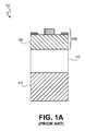
- a materialforms a buffer layer 170 between a silicon substrate 110 and a III-V device layer 180 .
- a semiconductor device 190is then fabricated in or upon device layer 180 .
- Various materialshave been utilized as the buffer layer 170 .
- AlSbaluminum antimonide
- strontium titanateSrTiO 3
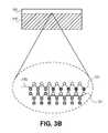
- these buffer layersare unable to prevent twins 171 , threading dislocations 173 and stacking faults 175 from propagating into the III-V device layer 180 as twins 181 , threading dislocations 183 , and stacking faults 185 .
- twins 171 , threading dislocations 173 and stacking faults 175from propagating into the III-V device layer 180 as twins 181 , threading dislocations 183 , and stacking faults 185 .
- FIG. 1Ais an illustration of a cross-sectional view of a conventional group III-V semiconductor device formed upon a silicon substrate.
- FIG. 1Bis an illustration of a cross-sectional view of a conventional group III-V semiconductor device layer formed upon a silicon substrate.
- FIG. 2is an illustration of a cross-sectional view of a group III-V semiconductor device layer formed upon a silicon substrate in accordance with the present invention.
- FIGS. 3A-3Dare illustrations of cross-sectional views of a method of fabricating a group III-V semiconductor device layer upon a silicon substrate in accordance with the present invention.
- FIGS. 4A-4Care illustrations of cross-sectional views of a method of fabricating a quantum well (QW) transistor in accordance with the present invention.
- FIG. 5is a flow diagram of a method of fabricating a group III-V semiconductor device layer upon a silicon substrate in accordance with the present invention.
- a stacking fault and twin blocking barrier for integrating III-V semiconductor devices on silicon substratesis described with reference to figures.
- certain embodimentsmay be practiced without one or more of these specific details, or in combination with other known methods and materials.
- numerous specific detailsare set forth, such as specific materials, dimensions and processes, etc., in order to provide a thorough understanding of the present invention.
- well-known semiconductor processes and manufacturing techniqueshave not been described in particular detail in order to not unnecessarily obscure the present invention.
- Reference throughout this specification to “an embodiment”means that a particular feature, structure, material, or characteristic described in connection with the embodiment is included in at least one embodiment of the invention.
- the appearances of the phrase “in an embodiment” in various places throughout this specificationare not necessarily referring to the same embodiment of the invention.
- the particular features, structures, materials, or characteristicsmay be combined in any suitable manner in one or more embodiments.
- Embodiments of the present inventionreduce the dislocations within the III-V device layer formed over a silicon substrate to near bulk-like quality by utilizing a buffer architecture and specific fabrication techniques tailored to the particular III-V device layer desired.
- a buffer architectureand specific fabrication techniques tailored to the particular III-V device layer desired.
- embodiments of the present inventionutilize a III-V semiconductor material buffer layer 240 formed between a silicon substrate 210 and III-V device layer 280 to form a semiconductor stack 200 .
- the III-V buffer layer 240 architectureis engineered for a particular III-V device layer material 280 with the materials for the III-V buffer layer 240 selected with consideration of lattice constant, band gap and melting point for the purpose of controlling nucleation and propagation of defects generated by lattice mismatch strain.
- the III-V buffer layer 240is formed on a vicinal surface of silicon substrate 210 having regular arrays of double-stepped (100) terraces across the substrate surface.
- a vicinal surfaceis a higher order crystal plane of the silicon substrate, such as, but not limited to the (211), (511), (013), (711) planes.
- a vicinal substrate surface having double-stepped terracesis capable of suppressing anti-phase domains (APD) in the III-V buffer layer 240 .
- An APDis created when a first polar crystal domain of layer 240 , having group III atoms attached to the nonpolar silicon substrate surface, meets a second polar crystal domain of layer 240 , having group V atoms attached to the silicon substrate.
- a crystal discontinuityforms in layer 240 at the border between these first and second domains providing recombination-generation centers detrimental to the operation of a semiconductor device.
- polarrefers to the partially ionic bonding character between the constituents of a III-V compound semiconductor.
- Embodiments providing the double atomic step in the silicon substrate 210provide for a terrace level of sufficient depth to prevent the growth species of buffer layer 240 from bonding to a higher level terrace even after all binding sites in the lowest terrace are occupied.
- the double step terraceprevents ad-hoc surface bonding so that the growth of the III-V buffer layer 240 proceeds in a stepwise fashion with each polar group III-V atomic bi-layer sequentially filling the lowest terrace of the nonpolar group IV, silicon substrate.
- anti-phase domainsare eliminated by growing layer 240 to a thickness greater than approximately 1.5 um.
- anti-phase domainsare substantially annihilated and a single domain film can be formed even on first order planes, such as, but not limited to, the (100) silicon substrates commonly used for microelectronic fabrication.
- a single domain layer 240is grown such a manner that the formation of anti-phase domains is avoided.
- layer 240may not be required to be thick, and may for example, be less than approximately 0.1 um in thickness using offcut Si substrate along with proper growth parameters such as growth rate, growth temperature and starting growth precursors.
- buffer layer 240 grown according to embodiments of this inventionmay be substantially free of stacking faults and twins.
- the phrase substantially free of stacking faults and twins as used hereinmeans that stacking fault and twin densities cannot be accurately measured using cross-section TEM or bandwidth TEM because such methods lose resolution below the detectible range of approximately 1 ⁇ 10 7 cm ⁇ 2 .
- the III-V buffer layer 240has a lattice spacing larger than the silicon substrate 210
- the III-V device layer 280has a lattice spacing larger than the III-V buffer layer 240
- buffer 240is comprised of a gallium antimonide (GaSb) layer 240 formed between the silicon substrate 210 and an indium antimonide (InSb) device layer 280 .
- GaSbgallium antimonide
- InSbindium antimonide
- the 6.09 ⁇ lattice constant of GaSb layer 240is approximately 12.2% larger than the 5.43 ⁇ lattice constant of the Silicon substrate 210 upon which layer 240 is formed.
- the 6.48 ⁇ lattice constant of the InSb layer 280is approximately 6.2% larger than the GaSb layer 240 .
- the lattice constant of the buffer 240incremented the lattice spacing of the silicon substrate 210 to the lattice spacing of the III-V device layer 280 , thereby partitioning the total lattice mismatch between two separate material interfaces.
- the InSb device layer 280need only accommodate the strain of a 6.2% lattice mismatch with GaSb layer 240 rather than the entire 19.2% mismatch with the silicon substrate 210 .
- III-V device layerssuch as, but not limited to, indium arsenide (InAs) device layers may be similarly integrated with silicon substrates using other buffer embodiments.
- III-V buffer layer 240is comprised of a gallium arsenide (GaAs) formed between the silicon substrate 210 and indium arsenide (InAs) device layer 280 to graduate the lattice constant in a manner analogous to that just described for the InSb embodiment.
- GaAsgallium arsenide
- InAsindium arsenide
- the buffer 240comprises materials which glide dislocations and terminate a significant percentage of the dislocations within the layer.
- the III-V buffer layer 240is comprised of a relatively narrow band gap III-V semiconductor material. Generally, the extent of dislocation glide is dependent on the hardness of the material, with glide occurring more readily in softer materials. Semiconductor materials of narrower band gap are typically softer, and it has been found more dislocation glide occurs in narrower band gap materials. Furthermore, more of the dislocations are terminated or contained as the thickness of a material capable of dislocation glides is increased.
- the III-V buffer layer 240is GaSb having a thickness between approximately 0.3 um and 5.0 um.
- GaSbreadily glides defects because the band gap of GaSb is relatively narrow, approximately 0.7 eV. Dislocation glide occurring within the GaSb changes the direction a defect propagates. This is particularly true for threading dislocations which typically propagate at an approximate sixty degree angle from the substrate surface. Gliding can change the direction of a threading dislocation to an angle more parallel to the surface of the film to terminate or contain the dislocations within the film as the buffer layer is thickened. For this reason, many of the defects induced by the strain of the 12.2% lattice mismatch between the silicon substrate 210 and a III-V buffer layer 240 of GaSb are glided and contained within the GaSb layer 240 . Because many such glided dislocations will not propagate into subsequently grown films, it is therefore possible to avoid simply accumulating defects within the subsequent epitaxial layers.
- the 6.09 ⁇ lattice constant of GaSb layer 240is approximately 12.2% larger than the 5.43 ⁇ lattice constant of the Silicon substrate 210 upon which layer 240 is formed. Because the band gap of GaSb is approximately 0.7 eV, the GaSb layer 240 is relatively soft and able to glide dislocations. In the same vein, it should be apparent that an embodiment utilizing GaSb provides better dislocation glide characteristics than an embodiment utilizing GaAs for the III-V buffer layer 240 because band gap of GaSb is lower than GaAs.
- the III-V buffer layer 240has a low melting point temperature which improves the thermal activation of dislocation glide within layer 240 during the subsequent layer growth. Dislocation glide reduces the propagation of threading dislocations, stacking faults and twins into the subsequent layers.
- a III-V buffer layer 240 of GaSbhas a melting point of approximately 712 C.
- the melting point of a GaAs layer 240is approximately 1237 C. Generally, the lower the melting point of the material, the better the dislocation glide.
- buffer 240allows for subsequent growth of a device layer 280 having an acceptably low final defect density.
- the buffer 240accommodates much of the 19.2% lattice mismatch between InSb device layer 280 and silicon substrate 210 to obtain a device layer having a threading dislocation defect density below 1 ⁇ 10 8 cm ⁇ 2 .
- the III-V device layer 280 of FIG. 2is of the desired material and of a sufficient thickness to achieve low defect density. Because the lattice spacing of the III-V device layer 280 is considered in the design of the buffer 240 , the III-V device layer 280 has significantly less lattice mismatch relative to the buffer 240 than to the silicon substrate 210 . A substantial portion of the defects in device layer 280 generated by lattice mismatch strain or propagated from the buffer 240 are glided within III-V device layer 280 as the thickness of 280 is increased.
- the device layer 280is grown to approximately 2.5 um thick to ensure defect density in the device layer 280 is below 1 ⁇ 10 8 cm ⁇ 2 .
- the device layer 280is grown to at least 7.5 um thick.
- the present embodimentsprovide for device-grade InSb on silicon substrates enabling electronic structures such as quantum well transistors to be formed on silicon substrates.
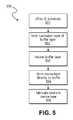
- FIG. 5is a flow diagram of a method to fabricate a III-V device layer in accordance with an embodiment of the present invention.
- Method 500 of FIG. 5begins with an offcut silicon substrate at step 501 .
- a nucleation layeris formed as the initial step of a two step process to form a buffer layer.
- the buffer layeris thickened with a growth process distinct from that used at step 502 .
- a III-V device layeris formed directly on the buffer and a device is fabricated in the III-V device layer at step 505 .
- FIGS. 3A-3DEach of these steps is discussed in greater detail below in reference to FIGS. 3A-3D .
- substrate 310has a vicinal surface, as shown in FIG. 3A .
- a vicinal surfaceis prepared by off-cutting the substrate from an ingot.
- the ingotis grown to provide wafer slices having (100) surfaces.
- the (100) substrate surfaceis then offcut at an angle between 2 and 12 degrees towards the [110] direction to produce a surface having terraces 312 .
- terraces 312include a surface having a (100) crystal plane.
- the (100) plane surface area of each terrace 312depends on the specific offcut angle, with a greater angle producing a greater number of terraces, each terrace having lesser (100) surface area.
- the offcutproduces a vicinal surface having an array of (100) terraces, many of which are separated by a double atomic step.
- a double step terracehas a height of two silicon atoms 311 .
- the silicon substrate offcut orientationsare (211), (511), (013), (711) and other high index planes.
- silicon substrate 310is without an offcut (zero degree offcut), such as, but not limited to, common (100) substrates. Such a substrate (not pictured) typically does not have a substantial number of double atomic step terraces.
- the III-V buffer layeris formed upon the silicon substrate 310 .
- Commonly known growth techniquesmay be used to form the III-V buffer layer, such as, but not limited to, metalorganic chemical vapor deposition (MOCVD) or molecular beam epitaxy (MBE).
- MOCVDmetalorganic chemical vapor deposition
- MBEmolecular beam epitaxy
- the bufferis formed in a manner that either avoids the formation of anti-phase domains (APD) or annihilates them as the film thickness is increased.
- APDanti-phase domains
- the III-V buffer layer 340is formed using a two step process, wherein the growth conditions of each step are distinct.
- a nucleation layer 320is formed in the first step.
- the growth of nucleation layer 320as shown in the expanded view, successively fills the lowest silicon substrate terraces with atomic bi-layers of the III-V semiconductor buffer material.
- the mobility of both the group III and group V species of the nucleation layer 320are sufficiently high that the atomic species introduced to the silicon surface travel about the surface of silicon substrate 310 and either fall into a terrace or completely off the silicon substrate surface.
- a species which falls down a terrace walllacks the energy to scale back up the terrace wall, therefore the otherwise substantially random species motion can be effectively funneled in a direction dictated by the substrate terracing.
- the silicon substrate bonding sitesare located by the mobile species until every site is filled. Because of the double atomic step in the silicon substrate 310 , a terrace completely filled with species 321 presents a single atomic step which the mobile species is unable to scale, and so excess species travel off the substrate surface without a significant number bonding to sites in the upper terrace levels. Subsequent introduction of the second species of the polar atomic pair is similarly funneled to the lowest terrace to bond with the first atomic species 321 to completely fill the lowest terrace with species 322 .
- the growth processthen proceeds in this iterative fashion until all terraces are filled and no nonpolar silicon substrate surface remains, at which point there is no longer risk of forming an APD in the polar buffer materials.
- the number of terraces which must be successively filledvaries. As the offcut angle increases, the number of terrace levels increases and the thickness of the nucleation layer must be increased to fill every terrace.
- the nucleation layer 320is between approximately 50 ⁇ and approximately 500 ⁇ . In some embodiments, the nucleation layer 320 is between approximately 30 ⁇ and approximately 300 ⁇ .
- a nucleation layer 320is formed using migration enhanced epitaxy (MEE) at a temperature of between 300 C and 600 C. MEE proceeds in a fashion similar to that of atomic layer deposition (ALD). MEE has a relatively slower growth rate, approximately 0.1 um/hr, because once the group V element is introduced to the substrate there is a hold time during which both the group V source and group III source shutters are closed (shuttered). This hold time accommodates the relatively lower mobility of the group V species.
- MEEmigration enhanced epitaxy
- ALDatomic layer deposition
- the substrate surfaceis exposed to an antimony (Sb) source for approximately 10 seconds to form a monolayer of Sb on the lowest terrace level.
- Sbantimony
- the Sb sourceand is then shuttered for a hold time of approximately 60 seconds.
- This relatively long hold timeallows for the Sb species to migrate on the surface of the silicon substrate to ensure the bonding sites of the lowest terrace level are filled.
- the substrate surfaceis exposed to a gallium (Ga) source for approximately 10 seconds. No hold time is required because of the high surface mobility of Ga.
- the Sbis reopened for approximately 10 second and then again closed for a hold time.
- GaSb nucleation temperaturesare in between 300 C. and 600 C.
- the MEE growth temperatureis between approximately 400 C. and approximately 510 C. Higher temperature embodiments enable a higher quality film.
- MEEcan be utilized to form a nucleation layer of an alternate buffer material, such as, but not limited to GaAs.
- a nucleation layer 320is formed on the vicinal silicon substrate 310 utilizing traditional MBE (without migration enhancement).
- MBEtraditional MBE
- the relatively higher flux of this particular embodiment using traditional MBEprovides higher film growth rates and therefore higher throughput than MEE embodiments.
- GaSbis formed on the silicon substrate 310 at a temperature between approximately 400 C. and approximately 510 C.
- the high-flux embodimentsare well suited to GaSb because of the relatively low vapor pressure and high sticking coefficient of antimony (Sb) as compared to arsenic (As) of GaAs films.
- a second growth stepcompletes the formation of the III-V buffer layer 340 .
- This second growth stepperformed at a higher temperature than that used for the nucleation layer 320 , forms layer 330 to thicken the III-V buffer layer 340 and glide dislocations.
- the film quality of layer 330is superior to that of the nucleation layer 320 because it is formed at a higher growth temperature.
- the flux ratecan be relatively high because the polar nucleation layer 320 eliminates any danger of APD formation.
- a GaSb film 330is grown upon a GaSb nucleation layer 320 at a growth temperature in the range of 500 C. and 700 C.
- a GaSb film 330is grown upon a GaSb nucleation layer 320 at a growth temperature between approximately 510 C. and approximately 570 C. In some embodiments of the present invention, the GaSb film 330 is grown to a thickness between approximately 0.3 um and 5.0 um. In an alternate embodiment, a GaAs film 330 is grown in a similar fashion upon a GaAs nucleation layer 320 .
- a thin buffer layer 340may function as a wetting layer, being only as thick as needed to bridge the non-polar/polar interface between the substrate 310 and buffer layer 340 , as well as avoid the formation of anti-phase domains. Because the buffer layer 340 is thin, it is less efficient at transferring strain into a subsequently deposited layer than a thick buffer layer 340 may be.
- the GaSb film 330is grown to a maximum thickness of 0.3 um. In yet another embodiment, the GaSb film 330 is grown to a maximum thickness of 0.1 um. In some embodiments it is desirable to have the entire GaSb buffer layer 340 , including nucleation layer 320 and layer 330 , below approximately 0.1 um.
- the III-V buffer layer 340is formed on a traditional silicon substrate 310 having a lower order plane surface, such as, but not limited to (100).
- the III-V buffer layer 340is grown without a nucleation step and permitted to form anti-phase domains.
- the single-step growthis performed at a temperature between 500 C. and 700 C. Once the film thickness is greater than approximately 1.5 um, the anti-phase domains, along with the stacking faults and twins, are substantially annihilated and the film becomes single-domain.
- a III-V buffer layer 340 comprising between approximately 1.5 and 2.0 um GaSbis formed on a traditional (100) silicon substrate 310 that has a 0 degree offcut.
- device layer 380is formed, as shown in FIG. 3D .
- Device layer 380is grown at a temperature appropriate for the particular III-V material desired.
- buffer layer 340comprises GaSb
- an InSb device layer 380is formed at a growth temperature between approximately 350 C. and approximately 475 C.
- the device layer 380is grown to a thickness sufficient to give an acceptable defect density.
- an InSb device layer 380is grown to a thickness greater than approximately 2 um.
- an InSb device layer 380is grown to a thickness of approximately 8 um to achieve a defect density of approximately 4 ⁇ 10 7 cm ⁇ 2 .
- the device layer 380may have a larger lattice constant material than the buffer layer 340 .
- buffer layer 340comprises GaSb with a lattice constant of approximately 6.09 ⁇
- the device layer 380may comprise InSb, which has a lattice constant of approximately 6.48 ⁇ .
- the GaSb buffer layer 340may induce a compressive stress into the larger lattice constant InSb device layer 380 .
- the larger lattice constant InSb device layer 380will retain the strain up until the device layer 380 reaches its critical thickness. Beyond the critical thickness, a lattice mismatched layer will relax, thus reducing strain.
- an InSb device layer 380 grown at less than 410 C.will have a critical thickness of approximately 100 ⁇ .
- the device layer 380may have a smaller lattice constant than the buffer layer 340 .
- the buffer layer 340comprises GaSb with a lattice constant of approximately 6.09 ⁇
- the device layer 380may be comprised of a smaller lattice constant material such as In x Ga 1-x As (x ⁇ 0.7, ⁇ 5.9 ⁇ ), InAs (6.06 ⁇ ), or InP (5.87 ⁇ ).
- a strained device layer 380may be detrimental to device performance.
- a tensilely strained device layer 380may be prone to cracking, thus introducing detrimental defects.
- the buffer layer 340may have a maximum thickness of less than approximately 0.3 um in order to reduce the amount of strain being induced in the device layer 380 .
- FIGS. 4A-4Cdepict embodiments of methods to fabricate a quantum well transistor in a III-V device layer on a substrate incorporating embodiments of the III-V buffer architecture discussed.
- FIG. 4Ashows device layer 480 comprising a quantum well 483 between an upper barrier layer 485 and a lower barrier layer 481 formed upon the buffer 440 over silicon substrate 410 .
- the lower barrier layer 481is formed of a higher band gap material than the overlying quantum well 483 .
- the lower barrier layer 481is of sufficient thickness to provide a potential barrier to charge carriers in the transistor channel.
- the lower barrier layer thicknessis between about 100 ⁇ and about 250 ⁇ .
- the lower barrieris InAlSb between 2500 ⁇ and 3000 ⁇ thick.
- lower barrier layer 481is microns thick to further reduce defect density in the quantum well 483 .
- the lower barrier layer 481is comprised of aluminum indium antimonide (Al x In 1-x Sb).
- the lower barrier layer 481is Al x In 1-x Sb with 15% aluminum.
- the lower barrier layer 481is comprised of indium aluminum arsenide (InAlAs).
- a quantum well 483is formed of a material with a smaller band gap than that of the lower barrier.
- the buffer 440comprises GaSb
- the quantum well 483is doped or undoped and formed of InSb.
- the buffer 440comprises GaAs
- the quantum well 483is doped or undoped and formed of indium gallium arsenide (In x Ga 1-x As) or InAs, as two examples.
- Quantum well 483is of a sufficient thickness to provide adequate channel conductance. In certain embodiments, the thickness of the quantum well 483 is between about 50 ⁇ and about 300 ⁇ .
- the upper barrier layer 485Over the quantum well 483 is the upper barrier layer 485 .
- Upper barrier layer 485has a larger band gap than the quantum well 483 , thereby confining a majority of charge carriers within the quantum well 483 for reduced device leakage.
- the upper barrier layer 485may be formed of the same or different materials as the lower barrier layer 481 .
- the upper barrier layer 485comprises aluminum indium antimonide (Al x In 1-x Sb).
- the upper barrier layer 485is Al x In 1-x Sb with 15% aluminum.
- the upper barrier layer 485comprises indium aluminum arsenide (InAlAs).
- the upper barrier layer 485may include a delta-doped layer (not shown) to supply carriers for embodiments where the lower quantum well is undoped (optionally the lower barrier 481 may be similarly doped to supply carriers).
- the delta dopingmay be done using silicon (Si) or tellurium (Te) impurities, as two examples.
- the upper barrier layer 485may have various thicknesses and in certain embodiments the upper barrier layer 485 is between about 40 ⁇ and 400 ⁇ thick.
- a highly-doped source drain layer 486is formed above the upper barrier layer 485 .
- the source drain layer 486is n+ doped InSb between about 30 ⁇ to about 300 ⁇ thick.
- source and drain contact metallizations 487are then formed by commonly known deposition processes, such as electron beam evaporation or reactive sputtering.
- a mask material 489is used to selectively remove a portion of the semiconductor device stack in preparation for the placement of the gate electrode.
- selective etchesmay be used to form a recess having a particular depth.
- source drain layer 486is removed during the gate recess etch to expose a suitable Schottky surface on the upper barrier layer 485 .
- Commonly known dry or wet etch techniquesmay be utilized to form the gate recess.
- the etchantmay be selective to the composition of the semiconductor, for example, in an embodiment, an n+ doped indium antimonide (InSb) source drain layer 486 is selectively removed using a wet etch process comprised of citric acid and peroxide.
- a wet etch processcomprised of citric acid and peroxide.
- the recess etch depthmay be tightly controlled by terminating on a stop layer grown upon the upper barrier layer 485 (not shown).
- the gate electrode 488is formed over the upper barrier layer 485 .
- commonly known techniquesare used to form the gate electrode 488 directly on the upper barrier layer 485 , thereby creating Schottky junction through which the gate controls the quantum well 483 .
- commonly known techniquesare used to form the gate electrode 488 on a dielectric layer over the upper barrier layer 485 , thereby creating a MOS junction.
- the gate electrode 488is formed using commonly known lift-off methods relying on lithography and highly directional deposition techniques, such as electron beam deposition, to separate the gate electrode 488 from the source drain layer 486 .
- the quantum well transistor 490is isolated using commonly known techniques.
- the epitaxial device layer of the quantum well transistor 490is etched through to form an active device mesa upon the buffer 440 over silicon substrate 410 .
- the isolation etchremoves the source drain layer 486 , upper barrier 485 , quantum well 483 and lower barrier 481 along a perimeter of the active device to form the mesa. This enables device isolation to be achieved with minimal topography.
- backend processingis performed using commonly known techniques to connect quantum well transistor 490 to the external environment.
Landscapes
- Engineering & Computer Science (AREA)
- Physics & Mathematics (AREA)
- Condensed Matter Physics & Semiconductors (AREA)
- General Physics & Mathematics (AREA)
- Manufacturing & Machinery (AREA)
- Computer Hardware Design (AREA)
- Microelectronics & Electronic Packaging (AREA)
- Power Engineering (AREA)
- Chemical & Material Sciences (AREA)
- Materials Engineering (AREA)
- Crystallography & Structural Chemistry (AREA)
- Recrystallisation Techniques (AREA)
Abstract
Description
The present application is a divisional of U.S. patent application Ser. No. 11/498,901 filed on Aug. 2, 2006, now U.S. Pat. No. 8,143,646 which is incorporated herein by reference.
1. Field of the Invention
The present invention relates to integrating III-V semiconductor devices upon silicon substrates. More particularly this invention relates to the buffer layer between a III-V semiconductor device and a silicon substrate.
2. Discussion of Related Art
A variety of electronic and optoelectronic devices can be enabled by developing thin film relaxed lattice constant III-V semiconductors on elemental silicon (Si) substrates. Surface layers capable of achieving the performance advantages of III-V materials may host a variety of high performance electronic devices such as CMOS and quantum well (QW) transistors fabricated from extreme high mobility materials such as, but not limited to, indium antimonide (InSb), indium gallium arsenide (InxGa1−xAs) (x>0.53) and indium arsenide (InAs). Optical devices such as lasers, detectors and photovoltaics may also be fabricated from various other direct band gap materials, such as, but not limited to, gallium arsenide (GaAs) and indium gallium arsenide (InGaAs). These devices can be further enhanced by monolithically integrating them with conventional devices of silicon and use of a silicon substrate has the additional advantage of cost reduction.
Despite all these advantages, the growth of III-V materials upon silicon substrates presents many challenges. Crystal defects are generated by lattice mismatch, polar-on-nonpolar mismatch and thermal mismatch between the III-V semiconductor epitaxial layer and the silicon semiconductor substrate. When the lattice mismatch between the epitaxial layer and substrate exceeds a few percent, the strain induced by the mismatch becomes too great and defects are generated in the epitaxial layer when the epitaxial film relaxes. Once the film thickness is greater than the critical thickness (film is strained below this thickness and relaxed above this thickness), the strain is relaxed by creating misfit dislocations at the film and substrate interface as well as in the epitaxial film. The epitaxial crystal defects are typically in the form of threading dislocations, stacking faults and twins (periodicity breaks where one portion of the lattice is a mirror image of another). Many defects, particularly threading dislocations, tend to propagate into the “device layer” where the semiconductor device is fabricated. Generally, the severity of defect generation correlates to the amount of lattice mismatch between the III-V semiconductor and the silicon substrate. For these reasons, the large lattice mismatch (approximately 19.2% between the exemplary indium antimonide (InSb) and silicon (Si) combination) typically results in an epitaxial device layer having a high defect density, on the order of 1×109cm−2to 1×1010cm−2. The high defect density reduces the carrier mobility theoretically possible in bulk InSb, eliminating many of the technical advantages of “InSb-on-silicon” integration. For example, the electron mobility in bulk InSb films is estimated to be approximately 76,000 cm2/Vs. However, to date, the best reported electron mobility of an InSb film formed over a silicon substrate is significantly lower, approximately 40,000-50,000 cm2/Vs.
Similarly, a high defect density is also detrimental to photonic devices formed in or upon III-V semiconductor device layers on silicon substrates. The recombination-generation (R-G) energies of crystal defects are typically mid-gap, detracting from the performance of a semiconductor device layer that has been band gap engineered for a particular optical wavelength.
Various buffer layers have been used in attempts to relieve the strain induced by the lattice mismatch between the silicon substrate and the III-V device layer and thereby reduce the detrimental defect density of the device layer. For example, as shown inapparatus 100 ofFIG. 1A , a material forms abuffer layer 170 between asilicon substrate 110 and a III-V device layer 180. Asemiconductor device 190 is then fabricated in or upondevice layer 180. Various materials have been utilized as thebuffer layer 170. For example, an aluminum antimonide (AlSb)buffer layer 170 has been attempted as has a strontium titanate (SrTiO3)buffer layer 170 between asilicon substrate 110 and a III-V device layer 180. In practice however, as depicted inFIG. 1B , these buffer layers are unable to preventtwins 171,threading dislocations 173 and stackingfaults 175 from propagating into the III-Vdevice layer 180 astwins 181,threading dislocations 183, andstacking faults 185. Thus, there remains a need for a buffer layer architecture that enables lower defect density III-V semiconductor device layers formed upon silicon substrates.
In various embodiments, a stacking fault and twin blocking barrier for integrating III-V semiconductor devices on silicon substrates is described with reference to figures. However, certain embodiments may be practiced without one or more of these specific details, or in combination with other known methods and materials. In the following description, numerous specific details are set forth, such as specific materials, dimensions and processes, etc., in order to provide a thorough understanding of the present invention. In other instances, well-known semiconductor processes and manufacturing techniques have not been described in particular detail in order to not unnecessarily obscure the present invention. Reference throughout this specification to “an embodiment” means that a particular feature, structure, material, or characteristic described in connection with the embodiment is included in at least one embodiment of the invention. Thus, the appearances of the phrase “in an embodiment” in various places throughout this specification are not necessarily referring to the same embodiment of the invention. Furthermore, the particular features, structures, materials, or characteristics may be combined in any suitable manner in one or more embodiments.
Embodiments of the present invention reduce the dislocations within the III-V device layer formed over a silicon substrate to near bulk-like quality by utilizing a buffer architecture and specific fabrication techniques tailored to the particular III-V device layer desired. As shown inFIG. 2 , embodiments of the present invention utilize a III-V semiconductor material buffer layer240 formed between asilicon substrate 210 and III-V device layer 280 to form asemiconductor stack 200. In embodiments of the present invention, the III-V buffer layer240 architecture is engineered for a particular III-Vdevice layer material 280 with the materials for the III-V buffer layer240 selected with consideration of lattice constant, band gap and melting point for the purpose of controlling nucleation and propagation of defects generated by lattice mismatch strain.
In particular embodiments, the III-V buffer layer240 is formed on a vicinal surface ofsilicon substrate 210 having regular arrays of double-stepped (100) terraces across the substrate surface. A vicinal surface is a higher order crystal plane of the silicon substrate, such as, but not limited to the (211), (511), (013), (711) planes. A vicinal substrate surface having double-stepped terraces is capable of suppressing anti-phase domains (APD) in the III-V buffer layer240. An APD is created when a first polar crystal domain of layer240, having group III atoms attached to the nonpolar silicon substrate surface, meets a second polar crystal domain of layer240, having group V atoms attached to the silicon substrate. A crystal discontinuity forms in layer240 at the border between these first and second domains providing recombination-generation centers detrimental to the operation of a semiconductor device. The term “polar” refers to the partially ionic bonding character between the constituents of a III-V compound semiconductor.
Embodiments providing the double atomic step in thesilicon substrate 210 provide for a terrace level of sufficient depth to prevent the growth species of buffer layer240 from bonding to a higher level terrace even after all binding sites in the lowest terrace are occupied. Thus, the double step terrace prevents ad-hoc surface bonding so that the growth of the III-V buffer layer240 proceeds in a stepwise fashion with each polar group III-V atomic bi-layer sequentially filling the lowest terrace of the nonpolar group IV, silicon substrate. In some embodiments, anti-phase domains are eliminated by growing layer240 to a thickness greater than approximately 1.5 um. At such thicknesses, anti-phase domains are substantially annihilated and a single domain film can be formed even on first order planes, such as, but not limited to, the (100) silicon substrates commonly used for microelectronic fabrication. In alternative embodiments, a single domain layer240 is grown such a manner that the formation of anti-phase domains is avoided. In such embodiments layer240 may not be required to be thick, and may for example, be less than approximately 0.1 um in thickness using offcut Si substrate along with proper growth parameters such as growth rate, growth temperature and starting growth precursors. Additionally, buffer layer240 grown according to embodiments of this invention may be substantially free of stacking faults and twins. The phrase substantially free of stacking faults and twins as used herein means that stacking fault and twin densities cannot be accurately measured using cross-section TEM or bandwidth TEM because such methods lose resolution below the detectible range of approximately 1×107cm−2.
In a particular embodiment, the III-V buffer layer240 has a lattice spacing larger than thesilicon substrate 210, and the III-V device layer 280 has a lattice spacing larger than the III-V buffer layer240. In one such an embodiment, buffer240 is comprised of a gallium antimonide (GaSb) layer240 formed between thesilicon substrate 210 and an indium antimonide (InSb)device layer 280. The 6.09 Å lattice constant of GaSb layer240 is approximately 12.2% larger than the 5.43 Å lattice constant of theSilicon substrate 210 upon which layer240 is formed. The 6.48 Å lattice constant of theInSb layer 280 is approximately 6.2% larger than the GaSb layer240. Thus, in this particular embodiment, the lattice constant of the buffer240 incremented the lattice spacing of thesilicon substrate 210 to the lattice spacing of the III-V device layer 280, thereby partitioning the total lattice mismatch between two separate material interfaces. In this manner, theInSb device layer 280 need only accommodate the strain of a 6.2% lattice mismatch with GaSb layer240 rather than the entire 19.2% mismatch with thesilicon substrate 210.
It should be appreciated that various III-V device layers, such as, but not limited to, indium arsenide (InAs) device layers may be similarly integrated with silicon substrates using other buffer embodiments. For example, in another embodiment of the present invention, III-V buffer layer240 is comprised of a gallium arsenide (GaAs) formed between thesilicon substrate 210 and indium arsenide (InAs)device layer 280 to graduate the lattice constant in a manner analogous to that just described for the InSb embodiment.
In embodiments of the present invention, the buffer240 comprises materials which glide dislocations and terminate a significant percentage of the dislocations within the layer. In particular embodiments, the III-V buffer layer240 is comprised of a relatively narrow band gap III-V semiconductor material. Generally, the extent of dislocation glide is dependent on the hardness of the material, with glide occurring more readily in softer materials. Semiconductor materials of narrower band gap are typically softer, and it has been found more dislocation glide occurs in narrower band gap materials. Furthermore, more of the dislocations are terminated or contained as the thickness of a material capable of dislocation glides is increased. In one particular embodiment, the III-V buffer layer240 is GaSb having a thickness between approximately 0.3 um and 5.0 um. GaSb readily glides defects because the band gap of GaSb is relatively narrow, approximately 0.7 eV. Dislocation glide occurring within the GaSb changes the direction a defect propagates. This is particularly true for threading dislocations which typically propagate at an approximate sixty degree angle from the substrate surface. Gliding can change the direction of a threading dislocation to an angle more parallel to the surface of the film to terminate or contain the dislocations within the film as the buffer layer is thickened. For this reason, many of the defects induced by the strain of the 12.2% lattice mismatch between thesilicon substrate 210 and a III-V buffer layer240 of GaSb are glided and contained within the GaSb layer240. Because many such glided dislocations will not propagate into subsequently grown films, it is therefore possible to avoid simply accumulating defects within the subsequent epitaxial layers.
As previously discussed, the 6.09 Å lattice constant of GaSb layer240 is approximately 12.2% larger than the 5.43 Å lattice constant of theSilicon substrate 210 upon which layer240 is formed. Because the band gap of GaSb is approximately 0.7 eV, the GaSb layer240 is relatively soft and able to glide dislocations. In the same vein, it should be apparent that an embodiment utilizing GaSb provides better dislocation glide characteristics than an embodiment utilizing GaAs for the III-V buffer layer240 because band gap of GaSb is lower than GaAs.
In embodiments of the present invention, the III-V buffer layer240 has a low melting point temperature which improves the thermal activation of dislocation glide within layer240 during the subsequent layer growth. Dislocation glide reduces the propagation of threading dislocations, stacking faults and twins into the subsequent layers. In a particular embodiment, for example, a III-V buffer layer240 of GaSb has a melting point of approximately 712 C. In another particular embodiment, the melting point of a GaAs layer240 is approximately 1237 C. Generally, the lower the melting point of the material, the better the dislocation glide.
In particular embodiments, buffer240 allows for subsequent growth of adevice layer 280 having an acceptably low final defect density. For such embodiments, the buffer240 accommodates much of the 19.2% lattice mismatch betweenInSb device layer 280 andsilicon substrate 210 to obtain a device layer having a threading dislocation defect density below 1×108cm−2.
In embodiments of the present invention, the III-V device layer 280 ofFIG. 2 is of the desired material and of a sufficient thickness to achieve low defect density. Because the lattice spacing of the III-V device layer 280 is considered in the design of the buffer240, the III-V device layer 280 has significantly less lattice mismatch relative to the buffer240 than to thesilicon substrate 210. A substantial portion of the defects indevice layer 280 generated by lattice mismatch strain or propagated from the buffer240 are glided within III-V device layer 280 as the thickness of280 is increased. In an embodiment of the present invention thedevice layer 280 is grown to approximately 2.5 um thick to ensure defect density in thedevice layer 280 is below 1×108cm−2. In another embodiment thedevice layer 280 is grown to at least 7.5 um thick. Thus, the present embodiments provide for device-grade InSb on silicon substrates enabling electronic structures such as quantum well transistors to be formed on silicon substrates.
Fabrication begins withsilicon substrate 310. In a particular embodiment,substrate 310 has a vicinal surface, as shown inFIG. 3A . A vicinal surface is prepared by off-cutting the substrate from an ingot. In one such embodiment, the ingot is grown to provide wafer slices having (100) surfaces. The (100) substrate surface is then offcut at an angle between 2 and 12 degrees towards the [110] direction to produce asurface having terraces 312.Terraces 312 include a surface having a (100) crystal plane. The (100) plane surface area of eachterrace 312 depends on the specific offcut angle, with a greater angle producing a greater number of terraces, each terrace having lesser (100) surface area. In such embodiments, the offcut produces a vicinal surface having an array of (100) terraces, many of which are separated by a double atomic step. As shown in the expanded view ofFIG. 3A , a double step terrace has a height of twosilicon atoms 311. In another embodiment, the silicon substrate offcut orientations are (211), (511), (013), (711) and other high index planes. Optionally,silicon substrate 310 is without an offcut (zero degree offcut), such as, but not limited to, common (100) substrates. Such a substrate (not pictured) typically does not have a substantial number of double atomic step terraces.
Next, the III-V buffer layer is formed upon thesilicon substrate 310. Commonly known growth techniques may be used to form the III-V buffer layer, such as, but not limited to, metalorganic chemical vapor deposition (MOCVD) or molecular beam epitaxy (MBE). As previously discussed, in particular embodiments, the buffer is formed in a manner that either avoids the formation of anti-phase domains (APD) or annihilates them as the film thickness is increased.
In a particular embodiment, as shown inFIG. 3B andFIG. 3C , the III-V buffer layer 340 is formed using a two step process, wherein the growth conditions of each step are distinct. In the first step, as shown inFIG. 3B , anucleation layer 320 is formed. The growth ofnucleation layer 320, as shown in the expanded view, successively fills the lowest silicon substrate terraces with atomic bi-layers of the III-V semiconductor buffer material. In this embodiment, the mobility of both the group III and group V species of thenucleation layer 320 are sufficiently high that the atomic species introduced to the silicon surface travel about the surface ofsilicon substrate 310 and either fall into a terrace or completely off the silicon substrate surface. A species which falls down a terrace wall lacks the energy to scale back up the terrace wall, therefore the otherwise substantially random species motion can be effectively funneled in a direction dictated by the substrate terracing. Once the species reaches the lowest terrace, the silicon substrate bonding sites are located by the mobile species until every site is filled. Because of the double atomic step in thesilicon substrate 310, a terrace completely filled withspecies 321 presents a single atomic step which the mobile species is unable to scale, and so excess species travel off the substrate surface without a significant number bonding to sites in the upper terrace levels. Subsequent introduction of the second species of the polar atomic pair is similarly funneled to the lowest terrace to bond with the firstatomic species 321 to completely fill the lowest terrace withspecies 322. The growth process then proceeds in this iterative fashion until all terraces are filled and no nonpolar silicon substrate surface remains, at which point there is no longer risk of forming an APD in the polar buffer materials. Thus, depending on the offcut angle of the substrate, the number of terraces which must be successively filled varies. As the offcut angle increases, the number of terrace levels increases and the thickness of the nucleation layer must be increased to fill every terrace. In particular embodiments, therefore, thenucleation layer 320 is between approximately 50 Å and approximately 500 Å. In some embodiments, thenucleation layer 320 is between approximately 30 Å and approximately 300 Å.
The high mobility required to ensure the terraces are successively filled is provided for by the growth parameters of thenucleation layer 320 and these parameters therefore depend on the particular mobility characteristics of species comprising the material oflayer 320. For example, in one embodiment, anucleation layer 320 is formed using migration enhanced epitaxy (MEE) at a temperature of between 300 C and 600 C. MEE proceeds in a fashion similar to that of atomic layer deposition (ALD). MEE has a relatively slower growth rate, approximately 0.1 um/hr, because once the group V element is introduced to the substrate there is a hold time during which both the group V source and group III source shutters are closed (shuttered). This hold time accommodates the relatively lower mobility of the group V species. No hold time is required for group III species because surface migration of this species relatively higher mobility. In a particular MEE embodiment, the substrate surface is exposed to an antimony (Sb) source for approximately 10 seconds to form a monolayer of Sb on the lowest terrace level. The Sb source and is then shuttered for a hold time of approximately 60 seconds. This relatively long hold time allows for the Sb species to migrate on the surface of the silicon substrate to ensure the bonding sites of the lowest terrace level are filled. Then, the substrate surface is exposed to a gallium (Ga) source for approximately 10 seconds. No hold time is required because of the high surface mobility of Ga. Next, the Sb is reopened for approximately 10 second and then again closed for a hold time. This process is repeated to form aGaSb nucleation layer 320 sufficiently thick to fill all the terraces of thesilicon substrate 310, approximately 150 Å in a particular embodiment. In an embodiment, GaSb nucleation temperatures are in between 300 C. and 600 C. In particular GaSb embodiment, the MEE growth temperature is between approximately 400 C. and approximately 510 C. Higher temperature embodiments enable a higher quality film. In other embodiments, MEE can be utilized to form a nucleation layer of an alternate buffer material, such as, but not limited to GaAs.
In yet another embodiment, anucleation layer 320 is formed on thevicinal silicon substrate 310 utilizing traditional MBE (without migration enhancement). The relatively higher flux of this particular embodiment using traditional MBE provides higher film growth rates and therefore higher throughput than MEE embodiments. In a particular MBE nucleation embodiment, GaSb is formed on thesilicon substrate 310 at a temperature between approximately 400 C. and approximately 510 C. The high-flux embodiments are well suited to GaSb because of the relatively low vapor pressure and high sticking coefficient of antimony (Sb) as compared to arsenic (As) of GaAs films.
Next, as shown inFIG. 3C , a second growth step completes the formation of the III-V buffer layer 340. This second growth step, performed at a higher temperature than that used for thenucleation layer 320, formslayer 330 to thicken the III-V buffer layer 340 and glide dislocations. The film quality oflayer 330 is superior to that of thenucleation layer 320 because it is formed at a higher growth temperature. Also, during the formation oflayer 330, the flux rate can be relatively high because thepolar nucleation layer 320 eliminates any danger of APD formation. In an embodiment, aGaSb film 330 is grown upon aGaSb nucleation layer 320 at a growth temperature in the range of 500 C. and 700 C. In a particular embodiment, aGaSb film 330 is grown upon aGaSb nucleation layer 320 at a growth temperature between approximately 510 C. and approximately 570 C. In some embodiments of the present invention, theGaSb film 330 is grown to a thickness between approximately 0.3 um and 5.0 um. In an alternate embodiment, aGaAs film 330 is grown in a similar fashion upon aGaAs nucleation layer 320.
In other embodiments of the present invention, it is preferred to have athin buffer layer 340. In some embodiments, athin buffer layer 340 may function as a wetting layer, being only as thick as needed to bridge the non-polar/polar interface between thesubstrate 310 andbuffer layer 340, as well as avoid the formation of anti-phase domains. Because thebuffer layer 340 is thin, it is less efficient at transferring strain into a subsequently deposited layer than athick buffer layer 340 may be. In one particular embodiment, theGaSb film 330 is grown to a maximum thickness of 0.3 um. In yet another embodiment, theGaSb film 330 is grown to a maximum thickness of 0.1 um. In some embodiments it is desirable to have the entireGaSb buffer layer 340, includingnucleation layer 320 andlayer 330, below approximately 0.1 um.
In still another embodiment, the III-V buffer layer 340 is formed on atraditional silicon substrate 310 having a lower order plane surface, such as, but not limited to (100). The III-V buffer layer 340 is grown without a nucleation step and permitted to form anti-phase domains. In an embodiment, the single-step growth is performed at a temperature between 500 C. and 700 C. Once the film thickness is greater than approximately 1.5 um, the anti-phase domains, along with the stacking faults and twins, are substantially annihilated and the film becomes single-domain. In a particular embodiment, a III-V buffer layer 340 comprising between approximately 1.5 and 2.0 um GaSb is formed on a traditional (100)silicon substrate 310 that has a 0 degree offcut.
Finally, with the completion of thebuffer 340,device layer 380 is formed, as shown inFIG. 3D .Device layer 380 is grown at a temperature appropriate for the particular III-V material desired. In a particular embodiment, whereinbuffer layer 340 comprises GaSb, anInSb device layer 380 is formed at a growth temperature between approximately 350 C. and approximately 475 C. Depending on the amount of lattice mismatch between thebuffer 340 and the III-V device layer 380, as well as the ability for the device layer to glide dislocations, thedevice layer 380 is grown to a thickness sufficient to give an acceptable defect density. In a particular embodiment, anInSb device layer 380 is grown to a thickness greater than approximately 2 um. In a further embodiment, anInSb device layer 380 is grown to a thickness of approximately 8 um to achieve a defect density of approximately 4×107cm−2.
In a particular embodiment, thedevice layer 380 may have a larger lattice constant material than thebuffer layer 340. For example, whereinbuffer layer 340 comprises GaSb with a lattice constant of approximately 6.09 Å, thedevice layer 380 may comprise InSb, which has a lattice constant of approximately 6.48 Å. In such an embodiment, theGaSb buffer layer 340 may induce a compressive stress into the larger lattice constantInSb device layer 380. The larger lattice constantInSb device layer 380 will retain the strain up until thedevice layer 380 reaches its critical thickness. Beyond the critical thickness, a lattice mismatched layer will relax, thus reducing strain. In one embodiment, anInSb device layer 380 grown at less than 410 C. will have a critical thickness of approximately 100 Å.
In another embodiment, thedevice layer 380 may have a smaller lattice constant than thebuffer layer 340. For example, wherein thebuffer layer 340 comprises GaSb with a lattice constant of approximately 6.09 Å, thedevice layer 380 may be comprised of a smaller lattice constant material such as InxGa1-xAs (x˜0.7, ˜5.9 Å), InAs (6.06 Å), or InP (5.87 Å). In such an embodiment, astrained device layer 380 may be detrimental to device performance. For example, a tensilelystrained device layer 380 may be prone to cracking, thus introducing detrimental defects. In an embodiment, where thedevice layer 380 has a smaller lattice constant than thebuffer layer 340, thebuffer layer 340 may have a maximum thickness of less than approximately 0.3 um in order to reduce the amount of strain being induced in thedevice layer 380.
Generally, thelower barrier layer 481 is formed of a higher band gap material than the overlying quantum well483. Thelower barrier layer 481 is of sufficient thickness to provide a potential barrier to charge carriers in the transistor channel. In a particular embodiment, the lower barrier layer thickness is between about 100 Å and about 250 Å. In other embodiments, the lower barrier is InAlSb between 2500 Å and 3000 Å thick. In still other embodiments,lower barrier layer 481 is microns thick to further reduce defect density in thequantum well 483. In certain embodiments wherein thebuffer 440 is comprised of a GaSb, thelower barrier layer 481 is comprised of aluminum indium antimonide (AlxIn1-xSb). In a particular embodiment, thelower barrier layer 481 is AlxIn1-xSb with 15% aluminum. In certain other embodiments wherein thebuffer 440 comprises GaAs, thelower barrier layer 481 is comprised of indium aluminum arsenide (InAlAs).
Then, over thelower barrier layer 481, aquantum well 483 is formed of a material with a smaller band gap than that of the lower barrier. In an embodiment wherein thebuffer 440 comprises GaSb, thequantum well 483 is doped or undoped and formed of InSb. In another embodiment wherein thebuffer 440 comprises GaAs, thequantum well 483 is doped or undoped and formed of indium gallium arsenide (InxGa1-xAs) or InAs, as two examples. Quantum well483 is of a sufficient thickness to provide adequate channel conductance. In certain embodiments, the thickness of thequantum well 483 is between about 50 Å and about 300 Å.
Over thequantum well 483 is theupper barrier layer 485.Upper barrier layer 485 has a larger band gap than thequantum well 483, thereby confining a majority of charge carriers within the quantum well483 for reduced device leakage. Theupper barrier layer 485 may be formed of the same or different materials as thelower barrier layer 481. In certain embodiments wherein thebuffer 440 comprises GaSb, theupper barrier layer 485 comprises aluminum indium antimonide (AlxIn1-xSb). In a particular embodiment, theupper barrier layer 485 is AlxIn1-xSb with 15% aluminum. In certain other embodiments, wherein thebuffer 440 comprises GaAs, theupper barrier layer 485 comprises indium aluminum arsenide (InAlAs). Theupper barrier layer 485 may include a delta-doped layer (not shown) to supply carriers for embodiments where the lower quantum well is undoped (optionally thelower barrier 481 may be similarly doped to supply carriers). For an n-type device utilizing an AlxIn1-xSbupper barrier 485, the delta doping may be done using silicon (Si) or tellurium (Te) impurities, as two examples. Theupper barrier layer 485 may have various thicknesses and in certain embodiments theupper barrier layer 485 is between about 40 Å and 400 Å thick.
Finally, to completedevice layer 480 as shown inFIG. 4A , a highly-dopedsource drain layer 486 is formed above theupper barrier layer 485. In a particular embodiment, thesource drain layer 486 is n+ doped InSb between about 30 Å to about 300 Å thick.
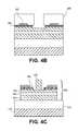
As shown inFIG. 4B , source and draincontact metallizations 487 are then formed by commonly known deposition processes, such as electron beam evaporation or reactive sputtering. In various embodiments, as shown inFIG. 4B , amask material 489 is used to selectively remove a portion of the semiconductor device stack in preparation for the placement of the gate electrode. Depending on whether a depletion mode or enhancement mode device is desired, selective etches may be used to form a recess having a particular depth. In particular embodiments,source drain layer 486 is removed during the gate recess etch to expose a suitable Schottky surface on theupper barrier layer 485. Commonly known dry or wet etch techniques may be utilized to form the gate recess. The etchant may be selective to the composition of the semiconductor, for example, in an embodiment, an n+ doped indium antimonide (InSb)source drain layer 486 is selectively removed using a wet etch process comprised of citric acid and peroxide. Through application of similar commonly known selective etch techniques, the recess etch depth may be tightly controlled by terminating on a stop layer grown upon the upper barrier layer485 (not shown).
As shown inFIG. 4C , thegate electrode 488 is formed over theupper barrier layer 485. In some embodiments of the present invention, commonly known techniques are used to form thegate electrode 488 directly on theupper barrier layer 485, thereby creating Schottky junction through which the gate controls thequantum well 483. In other embodiments, commonly known techniques are used to form thegate electrode 488 on a dielectric layer over theupper barrier layer 485, thereby creating a MOS junction. In particular embodiments, thegate electrode 488 is formed using commonly known lift-off methods relying on lithography and highly directional deposition techniques, such as electron beam deposition, to separate thegate electrode 488 from thesource drain layer 486.
Then, as shown inFIG. 4C , thequantum well transistor 490 is isolated using commonly known techniques. In particular embodiments, the epitaxial device layer of thequantum well transistor 490 is etched through to form an active device mesa upon thebuffer 440 oversilicon substrate 410. The isolation etch removes thesource drain layer 486,upper barrier 485,quantum well 483 andlower barrier 481 along a perimeter of the active device to form the mesa. This enables device isolation to be achieved with minimal topography. With thequantum well transistor 490 substantially complete, backend processing is performed using commonly known techniques to connectquantum well transistor 490 to the external environment.
Although the present invention has been described in language specific to structural features and/or methodological acts, it is to be understood that the invention defined in the appended claims is not necessarily limited to the specific features or acts described. The specific features and acts disclosed are instead to be understood as particularly graceful implementations of the claimed invention useful for illustrating the present invention.
Claims (10)
1. A method of forming a semiconductor structure comprising:
depositing a nucleation layer comprising Ga and Sb using migration enhanced epitaxy (MEE) at a first growth temperature and first growth rate of approximately 0.1 um/hr on a surface of a silicon substrate,
depositing a buffer layer consisting essentially of GaSb at a second growth temperature and second growth rate on the nucleation layer; and
forming a compound semiconductor device layer directly on the buffer layer;
wherein the second growth temperature is higher than the first growth temperature.
2. The method ofclaim 1 , wherein the surface is a (100) surface of the silicon substrate off-cut at an angle between 2 and 12 degrees towards a [110] direction.
3. The method ofclaim 1 , wherein the surface is off-cut from a plane selected from the group consisting of: (211), (511), (711), (013).
4. The method ofclaim 1 , wherein forming the compound semiconductor device layer upon the buffer layer further comprises depositing InSb at a growth temperature between approximately 300° C. and 500° C.
5. The method ofclaim 1 , wherein the surface of the silicon substrate upon which the nucleation layer is deposited is a vicinal surface comprising terraces, and wherein depositing the nucleation layer includes depositing alternating monolayers of Sb and Ga until the nucleation layer is sufficiently thick to fill substantially all the terraces of the vicinal surface.
6. The method ofclaim 1 , wherein the first growth temperature is between approximately 300° C. and 600° C.
7. The method ofclaim 1 , wherein the second growth temperature is approximately 510° C.
8. The method ofclaim 1 , wherein depositing the nucleation layer comprising Ga and Sb using migration enhanced epitaxy (MEE) comprises iterations of the following sequence: exposing the substrate to a Sb source, shuttering the Sb source, applying an approximately 60 second hold time in which both the Sb source and a Ga source are shuttered, exposing the substrate to the Ga source, shuttering the Ga source, and applying no hold time in which both the Sb source and the Ga source are shuttered.
9. A method of forming a compound semiconductor device layer on a silicon substrate comprising:
depositing GaSb upon a surface of the silicon substrate using migration enhanced epitaxy (MEE) at a first growth temperature and first growth rate of approximately 0.1 um/hr to form a GaSb nucleation layer, wherein the surface of the silicon substrate is off-cut from a (100) surface at an angle between 2 and 12 degrees toward a [110] direction;
depositing GaSb upon the GaSb nucleation layer at a second growth temperature and second growth rate to form a GaSb buffer layer, wherein the second growth temperature is higher than the first growth temperature; and
depositing an InSb device layer directly on the GaSb buffer layer.
10. The method ofclaim 9 , wherein depositing GaSb upon the surface of the silicon substrate using migration enhanced epitaxy (MEE) at the first growth temperature and first growth rate to form the GaSb nucleation layer comprises iterations of the following sequence: exposing the silicon substrate to a Sb source, shuttering the Sb source, applying an approximately 60 second hold time in which both the Sb source and a Ga source are shuttered, exposing the silicon substrate to the Ga source, shuttering the Ga source, and applying no hold time in which both the Sb source and the Ga source are shuttered.
Priority Applications (1)
| Application Number | Priority Date | Filing Date | Title |
|---|---|---|---|
| US13/366,143US8617945B2 (en) | 2006-08-02 | 2012-02-03 | Stacking fault and twin blocking barrier for integrating III-V on Si |
Applications Claiming Priority (2)
| Application Number | Priority Date | Filing Date | Title |
|---|---|---|---|
| US11/498,901US8143646B2 (en) | 2006-08-02 | 2006-08-02 | Stacking fault and twin blocking barrier for integrating III-V on Si |
| US13/366,143US8617945B2 (en) | 2006-08-02 | 2012-02-03 | Stacking fault and twin blocking barrier for integrating III-V on Si |
Related Parent Applications (1)
| Application Number | Title | Priority Date | Filing Date |
|---|---|---|---|
| US11/498,901DivisionUS8143646B2 (en) | 2006-08-02 | 2006-08-02 | Stacking fault and twin blocking barrier for integrating III-V on Si |
Publications (2)
| Publication Number | Publication Date |
|---|---|
| US20120142166A1 US20120142166A1 (en) | 2012-06-07 |
| US8617945B2true US8617945B2 (en) | 2013-12-31 |
Family
ID=39029718
Family Applications (2)
| Application Number | Title | Priority Date | Filing Date |
|---|---|---|---|
| US11/498,901Expired - Fee RelatedUS8143646B2 (en) | 2006-08-02 | 2006-08-02 | Stacking fault and twin blocking barrier for integrating III-V on Si |
| US13/366,143Expired - Fee RelatedUS8617945B2 (en) | 2006-08-02 | 2012-02-03 | Stacking fault and twin blocking barrier for integrating III-V on Si |
Family Applications Before (1)
| Application Number | Title | Priority Date | Filing Date |
|---|---|---|---|
| US11/498,901Expired - Fee RelatedUS8143646B2 (en) | 2006-08-02 | 2006-08-02 | Stacking fault and twin blocking barrier for integrating III-V on Si |
Country Status (1)
| Country | Link |
|---|---|
| US (2) | US8143646B2 (en) |
Cited By (3)
| Publication number | Priority date | Publication date | Assignee | Title |
|---|---|---|---|---|
| US20120086017A1 (en)* | 2009-06-15 | 2012-04-12 | Korea Electronics Technology Institute | Heterogeneous substrate, nitride-based semiconductor device using same, and manufacturing method thereof |
| WO2015147858A1 (en)* | 2014-03-28 | 2015-10-01 | Intel Corporation | Selective epitaxially grown iii-v materials based devices |
| US10304947B1 (en) | 2017-11-30 | 2019-05-28 | International Business Machines Corporation | Smoothing surface roughness of III-V semiconductor fins formed from silicon mandrels by regrowth |
Families Citing this family (28)
| Publication number | Priority date | Publication date | Assignee | Title |
|---|---|---|---|---|
| US8809867B2 (en)* | 2002-04-15 | 2014-08-19 | The Regents Of The University Of California | Dislocation reduction in non-polar III-nitride thin films |
| US8183556B2 (en) | 2005-12-15 | 2012-05-22 | Intel Corporation | Extreme high mobility CMOS logic |
| US8143646B2 (en) | 2006-08-02 | 2012-03-27 | Intel Corporation | Stacking fault and twin blocking barrier for integrating III-V on Si |
| US7851780B2 (en)* | 2006-08-02 | 2010-12-14 | Intel Corporation | Semiconductor buffer architecture for III-V devices on silicon substrates |
| US8278687B2 (en)* | 2008-03-28 | 2012-10-02 | Intel Corporation | Semiconductor heterostructures to reduce short channel effects |
| US8129749B2 (en)* | 2008-03-28 | 2012-03-06 | Intel Corporation | Double quantum well structures for transistors |
| US20100148153A1 (en)* | 2008-12-16 | 2010-06-17 | Hudait Mantu K | Group III-V devices with delta-doped layer under channel region |
| US8440998B2 (en) | 2009-12-21 | 2013-05-14 | Intel Corporation | Increasing carrier injection velocity for integrated circuit devices |
| US7892902B1 (en) | 2009-12-22 | 2011-02-22 | Intel Corporation | Group III-V devices with multiple spacer layers |
| US8633470B2 (en)* | 2009-12-23 | 2014-01-21 | Intel Corporation | Techniques and configurations to impart strain to integrated circuit devices |
| US8216943B2 (en) | 2010-06-29 | 2012-07-10 | Micron Technology, Inc. | Epitaxial growth method |
| CN102157903B (en)* | 2011-01-25 | 2012-08-08 | 中国科学院半导体研究所 | Epitaxial growth method of W type antimonide class II quantum well |
| CN102427068B (en)* | 2011-12-02 | 2014-06-18 | 中国科学院上海微系统与信息技术研究所 | Monolithical integration lattice mismatched crystal template and manufacturing method thereof |
| US8603898B2 (en) | 2012-03-30 | 2013-12-10 | Applied Materials, Inc. | Method for forming group III/V conformal layers on silicon substrates |
| EP2804203A1 (en) | 2013-05-17 | 2014-11-19 | Imec | III-V device and method for manufacturing thereof |
| CN105308719B (en) | 2013-06-28 | 2019-07-26 | 英特尔公司 | Device based on selective epitaxial growth of III-V materials |
| GB201321949D0 (en) | 2013-12-12 | 2014-01-29 | Ibm | Semiconductor nanowire fabrication |
| US9293523B2 (en) | 2014-06-24 | 2016-03-22 | Applied Materials, Inc. | Method of forming III-V channel |
| WO2016069181A1 (en)* | 2014-10-30 | 2016-05-06 | Applied Materials, Inc. | Method and structure to improve film stack with sensitive and reactive layers |
| US9406506B2 (en) | 2014-11-05 | 2016-08-02 | International Business Machines Corporation | Lattice matched aspect ratio trapping to reduce defects in III-V layer directly grown on silicon |
| US9728671B2 (en)* | 2014-11-14 | 2017-08-08 | International Business Machines Corporation | Monolithic nano-cavity light source on lattice mismatched semiconductor substrate |
| US10043666B2 (en)* | 2016-02-26 | 2018-08-07 | Applied Materials, Inc. | Method for inter-chamber process |
| US9735010B1 (en) | 2016-05-27 | 2017-08-15 | International Business Machines Corporation | Fabrication of semiconductor fin structures |
| US10249492B2 (en) | 2016-05-27 | 2019-04-02 | International Business Machines Corporation | Fabrication of compound semiconductor structures |
| WO2017213651A1 (en)* | 2016-06-09 | 2017-12-14 | Intel Corporation | Quantum dot devices with top gates |
| TWI670469B (en)* | 2018-08-24 | 2019-09-01 | 超能高新材料股份有限公司 | Crystal quality determination method |
| CN113314398B (en)* | 2021-05-25 | 2024-02-06 | 中国科学院苏州纳米技术与纳米仿生研究所 | Method for epitaxial growth of InGaAs film on GaP/Si substrate and InGaAs film |
| CN116598395B (en)* | 2023-07-14 | 2023-09-29 | 江西兆驰半导体有限公司 | A kind of light-emitting diode and preparation method thereof |
Citations (435)
| Publication number | Priority date | Publication date | Assignee | Title |
|---|---|---|---|---|
| US4231149A (en) | 1978-10-10 | 1980-11-04 | Texas Instruments Incorporated | Narrow band-gap semiconductor CCD imaging device and method of fabrication |
| US4487652A (en) | 1984-03-30 | 1984-12-11 | Motorola, Inc. | Slope etch of polyimide |
| GB2156149A (en) | 1984-03-14 | 1985-10-02 | Philips Electronic Associated | Dielectrically-isolated integrated circuit manufacture |
| US4711701A (en) | 1986-09-16 | 1987-12-08 | Texas Instruments Incorporated | Self-aligned transistor method |
| EP0265314A1 (en) | 1986-10-06 | 1988-04-27 | France Telecom | Method of forming an insulating layer of a sulphide, sulphur compounds obtained and device to carry out the method |
| US4751201A (en) | 1987-03-04 | 1988-06-14 | Bell Communications Research, Inc. | Passivation of gallium arsenide devices with sodium sulfide |
| US4818715A (en) | 1987-07-09 | 1989-04-04 | Industrial Technology Research Institute | Method of fabricating a LDDFET with self-aligned silicide |
| US4872046A (en) | 1986-01-24 | 1989-10-03 | University Of Illinois | Heterojunction semiconductor device with <001> tilt |
| US4871692A (en) | 1988-09-30 | 1989-10-03 | Lee Hong H | Passivation of group III-V surfaces |
| US4905063A (en) | 1988-06-21 | 1990-02-27 | American Telephone And Telegraph Company, At&T Bell Laboratories | Floating gate memories |
| US4906589A (en) | 1989-02-06 | 1990-03-06 | Industrial Technology Research Institute | Inverse-T LDDFET with self-aligned silicide |
| US4907048A (en) | 1987-11-23 | 1990-03-06 | Xerox Corporation | Double implanted LDD transistor self-aligned with gate |
| US4914059A (en) | 1986-10-27 | 1990-04-03 | Yves Nissim | Process for the heat flash vapour phase deposition of an insulating layer on a III-V material substrate and its application to the production of a MIS structure |
| US4994873A (en) | 1988-10-17 | 1991-02-19 | Motorola, Inc. | Local interconnect for stacked polysilicon device |
| US4996574A (en) | 1988-07-01 | 1991-02-26 | Fujitsu Limited | MIS transistor structure for increasing conductance between source and drain regions |
| US5023203A (en) | 1988-07-28 | 1991-06-11 | Korea Electronics & Telecommunications Research Institute Et Al. | Method of patterning fine line width semiconductor topology using a spacer |
| EP0469604A2 (en) | 1990-08-01 | 1992-02-05 | Sumitomo Electric Industries, Limited | MIS electrode forming process |
| EP0474952A1 (en) | 1990-09-14 | 1992-03-18 | International Business Machines Corporation | A method of passivating etched mirror facets of semiconductor lasers |
| US5120666A (en) | 1989-05-16 | 1992-06-09 | Fujitsu Limited | Manufacturing method for semiconductor device |
| US5124777A (en) | 1990-07-02 | 1992-06-23 | Samsung Electronics Co., Ltd. | Dielectric medium for capacitor of semiconductor device |
| US5141893A (en)* | 1988-12-22 | 1992-08-25 | Ford Microelectronics | Growth of P type Group III-V compound semiconductor on Group IV semiconductor substrate |
| US5144378A (en) | 1990-03-06 | 1992-09-01 | Fujitsu Limited | High electron mobility transistor |
| US5179037A (en) | 1991-12-24 | 1993-01-12 | Texas Instruments Incorporated | Integration of lateral and vertical quantum well transistors in the same epitaxial stack |
| US5216271A (en) | 1990-09-28 | 1993-06-01 | Kabushiki Kaisha Toshiba | BiCMOS device with low bandgap CMOS contact regions and low bandgap bipolar base region |
| US5278102A (en) | 1990-08-18 | 1994-01-11 | Fujitsu Limited | SOI device and a fabrication process thereof |
| US5308999A (en) | 1992-02-27 | 1994-05-03 | Fujitsu Limited | MOS FET having a thin film SOI structure |
| US5328810A (en) | 1990-05-07 | 1994-07-12 | Micron Technology, Inc. | Method for reducing, by a factor or 2-N, the minimum masking pitch of a photolithographic process |
| US5338959A (en) | 1992-03-30 | 1994-08-16 | Samsung Electronics Co., Ltd. | Thin film transistor with three dimensional multichannel structure |
| US5346839A (en) | 1991-06-10 | 1994-09-13 | Texas Instruments Incorporated | Sidewall doping technique for SOI transistors |
| US5346836A (en) | 1991-06-06 | 1994-09-13 | Micron Technology, Inc. | Process for forming low resistance contacts between silicide areas and upper level polysilicon interconnects |
| US5357119A (en) | 1993-02-19 | 1994-10-18 | Board Of Regents Of The University Of California | Field effect devices having short period superlattice structures using Si and Ge |
| EP0623963A1 (en) | 1993-05-06 | 1994-11-09 | Siemens Aktiengesellschaft | MOSFET on SOI substrate |
| US5391506A (en) | 1992-01-31 | 1995-02-21 | Kawasaki Steel Corporation | Manufacturing method for semiconductor devices with source/drain formed in substrate projection. |
| US5428237A (en) | 1991-04-26 | 1995-06-27 | Canon Kabushiki Kaisha | Semiconductor device having an insulated gate transistor |
| US5466621A (en) | 1988-11-21 | 1995-11-14 | Hitachi, Ltd. | Method of manufacturing a semiconductor device having silicon islands |
| US5475869A (en) | 1993-05-28 | 1995-12-12 | Nec Corporation | Radio base station capable of distinguishing between interference due to collisions of outgoing call signals and an external interference noise |
| US5479033A (en) | 1994-05-27 | 1995-12-26 | Sandia Corporation | Complementary junction heterostructure field-effect transistor |
| US5482877A (en) | 1993-02-17 | 1996-01-09 | Samsung Electronics Co., Ltd. | Method for making a semiconductor device having a silicon-on-insulator structure |
| US5495115A (en) | 1993-08-06 | 1996-02-27 | Hitachi, Ltd. | Semiconductor crystalline laminate structure, forming method of the same, and semiconductor device employing the same |
| US5514885A (en) | 1986-10-09 | 1996-05-07 | Myrick; James J. | SOI methods and apparatus |
| US5521859A (en) | 1991-03-20 | 1996-05-28 | Fujitsu Limited | Semiconductor memory device having thin film transistor and method of producing the same |
| US5543351A (en) | 1992-03-19 | 1996-08-06 | Matsushita Electric Industrial Co., Ltd. | Method of producing electrically insulated silicon structure |
| US5545586A (en) | 1990-11-27 | 1996-08-13 | Nec Corporation | Method of making a transistor having easily controllable impurity profile |
| US5563077A (en) | 1992-04-24 | 1996-10-08 | Hyundai Electronics Industries Co., Ltd. | Method of fabricating a thin film transistor having vertical channel |
| US5576227A (en) | 1994-11-02 | 1996-11-19 | United Microelectronics Corp. | Process for fabricating a recessed gate MOS device |
| US5578513A (en) | 1993-09-17 | 1996-11-26 | Mitsubishi Denki Kabushiki Kaisha | Method of making a semiconductor device having a gate all around type of thin film transistor |
| US5595919A (en) | 1996-02-20 | 1997-01-21 | Chartered Semiconductor Manufacturing Pte Ltd. | Method of making self-aligned halo process for reducing junction capacitance |
| US5595941A (en) | 1994-06-01 | 1997-01-21 | Mitsubishi Denki Kabushiki Kaisha | Method of forming fine patterns |
| US5652454A (en) | 1993-07-05 | 1997-07-29 | Iwamatsu; Toshiaki | Semiconductor device on an SOI substrate |
| US5658806A (en) | 1995-10-26 | 1997-08-19 | National Science Council | Method for fabricating thin-film transistor with bottom-gate or dual-gate configuration |
| US5665203A (en) | 1995-04-28 | 1997-09-09 | International Business Machines Corporation | Silicon etching method |
| US5682048A (en) | 1995-05-19 | 1997-10-28 | Nissan Motor Co., Ltd. | Groove-type semiconductor device |
| US5698869A (en) | 1994-09-13 | 1997-12-16 | Kabushiki Kaisha Toshiba | Insulated-gate transistor having narrow-bandgap-source |
| US5701016A (en) | 1994-11-24 | 1997-12-23 | Kabushiki Kaisha Toshiba | Semiconductor device and method for its manufacture |
| US5716879A (en) | 1994-12-15 | 1998-02-10 | Goldstar Electron Company, Ltd. | Method of making a thin film transistor |
| US5739544A (en) | 1993-05-26 | 1998-04-14 | Matsushita Electric Industrial Co., Ltd. | Quantization functional device utilizing a resonance tunneling effect and method for producing the same |
| US5760442A (en) | 1994-09-29 | 1998-06-02 | Kabushiki Kaisha Toshiba | Semiconductor device of a silicon on insulator metal-insulator type with a concave feature |
| US5770513A (en) | 1993-02-25 | 1998-06-23 | Mitsubishi Denki Kabushiki Kaisha | Method for producing semiconductor device with heat dissipation structure |
| US5773331A (en) | 1996-12-17 | 1998-06-30 | International Business Machines Corporation | Method for making single and double gate field effect transistors with sidewall source-drain contacts |
| US5776821A (en) | 1997-08-22 | 1998-07-07 | Vlsi Technology, Inc. | Method for forming a reduced width gate electrode |
| US5793088A (en) | 1996-06-18 | 1998-08-11 | Integrated Device Technology, Inc. | Structure for controlling threshold voltage of MOSFET |
| US5804848A (en) | 1995-01-20 | 1998-09-08 | Sony Corporation | Field effect transistor having multiple gate electrodes surrounding the channel region |
| US5811324A (en) | 1995-12-26 | 1998-09-22 | Lg Semicon Co., Ltd. | Method for manufacturing thin film transistor |
| US5814895A (en) | 1995-12-22 | 1998-09-29 | Sony Corporation | Static random access memory having transistor elements formed on side walls of a trench in a semiconductor substrate |
| US5821629A (en) | 1994-10-04 | 1998-10-13 | United Microelectronics Corporation | Buried structure SRAM cell and methods for fabrication |
| US5827769A (en) | 1996-11-20 | 1998-10-27 | Intel Corporation | Method for fabricating a transistor with increased hot carrier resistance by nitridizing and annealing the sidewall oxide of the gate electrode |
| US5838029A (en)* | 1994-08-22 | 1998-11-17 | Rohm Co., Ltd. | GaN-type light emitting device formed on a silicon substrate |
| US5844278A (en) | 1994-09-14 | 1998-12-01 | Kabushiki Kaisha Toshiba | Semiconductor device having a projecting element region |
| US5856225A (en) | 1997-11-24 | 1999-01-05 | Chartered Semiconductor Manufacturing Ltd | Creation of a self-aligned, ion implanted channel region, after source and drain formation |
| US5859456A (en) | 1994-11-02 | 1999-01-12 | Texas Instruments Incorporated | Multiple transistor integrated circuit with thick copper interconnect |
| US5880015A (en) | 1991-04-30 | 1999-03-09 | Sgs-Thomson Microelectronics, Inc. | Method of producing stepped wall interconnects and gates |
| US5883564A (en) | 1994-04-18 | 1999-03-16 | General Motors Corporation | Magnetic field sensor having high mobility thin indium antimonide active layer on thin aluminum indium antimonide buffer layer |
| US5888309A (en) | 1997-12-29 | 1999-03-30 | Taiwan Semiconductor Manufacturing Company, Ltd. | Lateral etch inhibited multiple for forming a via through a microelectronics layer susceptible to etching within a fluorine containing plasma followed by an oxygen containing plasma |
| US5889304A (en) | 1996-06-28 | 1999-03-30 | Kabushiki Kaisha Toshiba | Nonvolatile semiconductor memory device |
| US5905285A (en) | 1996-09-12 | 1999-05-18 | Advanced Micro Devices, Inc. | Ultra short trench transistors and process for making same |
| US5908313A (en) | 1996-12-31 | 1999-06-01 | Intel Corporation | Method of forming a transistor |
| US5952701A (en) | 1997-08-18 | 1999-09-14 | National Semiconductor Corporation | Design and fabrication of semiconductor structure having complementary channel-junction insulated-gate field-effect transistors whose gate electrodes have work functions close to mid-gap semiconductor value |
| US5965914A (en) | 1997-06-18 | 1999-10-12 | Mitsubishi Denki Kabushiki Kaisha | Thin film transistor having a branched gate and channel |
| US5976767A (en) | 1997-10-09 | 1999-11-02 | Micron Technology, Inc. | Ammonium hydroxide etch of photoresist masked silicon |
| US5981400A (en) | 1997-09-18 | 1999-11-09 | Cornell Research Foundation, Inc. | Compliant universal substrate for epitaxial growth |
| US5985726A (en) | 1998-11-06 | 1999-11-16 | Advanced Micro Devices, Inc. | Damascene process for forming ultra-shallow source/drain extensions and pocket in ULSI MOSFET |
| US6013926A (en) | 1996-11-20 | 2000-01-11 | Mitsubishi Denki Kabushiki Kaisha | Semiconductor device with refractory metal element |
| US6018176A (en) | 1995-05-26 | 2000-01-25 | Samsung Electronics Co., Ltd. | Vertical transistor and memory cell |
| JP2000037842A (en) | 1998-07-27 | 2000-02-08 | Dainippon Printing Co Ltd | Electromagnetic wave absorbing cosmetic material |
| US6031249A (en) | 1996-07-11 | 2000-02-29 | Semiconductor Energy Laboratory Co., Ltd. | CMOS semiconductor device having boron doped channel |
| US6054355A (en) | 1997-06-30 | 2000-04-25 | Kabushiki Kaisha Toshiba | Method of manufacturing a semiconductor device which includes forming a dummy gate |
| US6063677A (en) | 1996-10-28 | 2000-05-16 | Texas Instruments Incorporated | Method of forming a MOSFET using a disposable gate and raised source and drain |
| US6063675A (en) | 1996-10-28 | 2000-05-16 | Texas Instruments Incorporated | Method of forming a MOSFET using a disposable gate with a sidewall dielectric |
| US6066869A (en) | 1997-10-06 | 2000-05-23 | Micron Technology, Inc. | Circuit and method for a folded bit line memory cell with vertical transistor and trench capacitor |
| US6087208A (en) | 1998-03-31 | 2000-07-11 | Advanced Micro Devices, Inc. | Method for increasing gate capacitance by using both high and low dielectric gate material |
| US6093621A (en) | 1999-04-05 | 2000-07-25 | Vanguard International Semiconductor Corp. | Method of forming shallow trench isolation |
| US6114201A (en) | 1998-06-01 | 2000-09-05 | Texas Instruments-Acer Incorporated | Method of manufacturing a multiple fin-shaped capacitor for high density DRAMs |
| US6114206A (en) | 1998-11-06 | 2000-09-05 | Advanced Micro Devices, Inc. | Multiple threshold voltage transistor implemented by a damascene process |
| US6117741A (en) | 1998-01-09 | 2000-09-12 | Texas Instruments Incorporated | Method of forming a transistor having an improved sidewall gate structure |
| US6117697A (en) | 1998-07-27 | 2000-09-12 | The United States Of America As Represented By The Secretary Of The Air Force | Solid state magnetic field sensor method |
| US6120846A (en) | 1997-12-23 | 2000-09-19 | Advanced Technology Materials, Inc. | Method for the selective deposition of bismuth based ferroelectric thin films by chemical vapor deposition |
| US6133593A (en) | 1999-07-23 | 2000-10-17 | The United States Of America As Represented By The Secretary Of The Navy | Channel design to reduce impact ionization in heterostructure field-effect transistors |
| US6144072A (en) | 1994-11-02 | 2000-11-07 | Mitsubishi Denki Kabushiki Kaisha | Semiconductor device formed on insulating layer and method of manufacturing the same |
| US6150222A (en) | 1999-01-07 | 2000-11-21 | Advanced Micro Devices, Inc. | Method of making a high performance transistor with elevated spacer formation and self-aligned channel regions |
| US6153485A (en) | 1998-11-09 | 2000-11-28 | Chartered Semiconductor Manufacturing Ltd. | Salicide formation on narrow poly lines by pulling back of spacer |
| US6163053A (en) | 1996-11-06 | 2000-12-19 | Ricoh Company, Ltd. | Semiconductor device having opposite-polarity region under channel |
| US6165880A (en) | 1998-06-15 | 2000-12-26 | Taiwan Semiconductor Manufacturing Company | Double spacer technology for making self-aligned contacts (SAC) on semiconductor integrated circuits |
| US6174820B1 (en) | 1999-02-16 | 2001-01-16 | Sandia Corporation | Use of silicon oxynitride as a sacrificial material for microelectromechanical devices |
| US6190975B1 (en) | 1996-09-17 | 2001-02-20 | Matsushita Electric Industrial Co., Ltd. | Method of forming HCMOS devices with a silicon-germanium-carbon compound semiconductor layer |
| US6200865B1 (en) | 1998-12-04 | 2001-03-13 | Advanced Micro Devices, Inc. | Use of sacrificial dielectric structure to form semiconductor device with a self-aligned threshold adjust and overlying low-resistance gate |
| US6218309B1 (en) | 1999-06-30 | 2001-04-17 | Lam Research Corporation | Method of achieving top rounding and uniform etch depths while etching shallow trench isolation features |
| US6252262B1 (en) | 1998-12-15 | 2001-06-26 | The United States Of America As Represented By The Secretary Of The Navy | Metal passivating layer for III-V semiconductors, and improved gate contact for III-V-based metal-insulator-semiconductor (MIS) devices |
| US6251763B1 (en) | 1997-06-30 | 2001-06-26 | Kabushiki Kaisha Toshiba | Semiconductor device and method for manufacturing same |
| US6251729B1 (en) | 1998-12-18 | 2001-06-26 | U.S. Philips Corporation | Method of manufacturing a nonvolatile memory |
| JP2001189453A (en) | 1999-10-06 | 2001-07-10 | Lsi Logic Corp | Fully depleted, fully inverted, vertical channel, short and dual gate CMOS field effect transistors |
| US6259135B1 (en) | 1999-09-24 | 2001-07-10 | International Business Machines Corporation | MOS transistors structure for reducing the size of pitch limited circuits |
| US6262456B1 (en) | 1998-11-06 | 2001-07-17 | Advanced Micro Devices, Inc. | Integrated circuit having transistors with different threshold voltages |
| US6261921B1 (en) | 1999-07-31 | 2001-07-17 | Taiwan Semiconductor Manufacturing Co., Ltd. | Method of forming shallow trench isolation structure |
| US6274503B1 (en) | 1998-12-18 | 2001-08-14 | United Microelectronics Corp. | Etching method for doped polysilicon layer |
| US20010019886A1 (en) | 1998-05-12 | 2001-09-06 | International Business Machines Corporation | Borderless contact to diffusion with respect to gate conductor and methods for fabricating |
| US6287924B1 (en) | 1998-09-21 | 2001-09-11 | Texas Instruments Incorporated | Integrated circuit and method |
| US6294416B1 (en) | 1998-01-23 | 2001-09-25 | Texas Instruments-Acer Incorporated | Method of fabricating CMOS transistors with self-aligned planarization twin-well by using fewer mask counts |
| US20010026985A1 (en) | 2000-03-29 | 2001-10-04 | Kim Moon Jung | Fabrication method of submicron gate using anisotropic etching |
| US6307235B1 (en) | 1998-03-30 | 2001-10-23 | Micron Technology, Inc. | Another technique for gated lateral bipolar transistors |
| US6310367B1 (en) | 1999-02-22 | 2001-10-30 | Kabushiki Kaisha Toshiba | MOS transistor having a tensile-strained SI layer and a compressive-strained SI-GE layer |
| US20010040907A1 (en) | 1998-06-12 | 2001-11-15 | Utpal Kumar Chakrabarti | Optical device including carbon-doped contact layers |
| US6320212B1 (en) | 1999-09-02 | 2001-11-20 | Hrl Laboratories, Llc. | Superlattice fabrication for InAs/GaSb/AISb semiconductor structures |
| US6319807B1 (en) | 2000-02-07 | 2001-11-20 | United Microelectronics Corp. | Method for forming a semiconductor device by using reverse-offset spacer process |
| JP2001338987A (en) | 2000-05-26 | 2001-12-07 | Nec Microsystems Ltd | Forming method of shallow trench isolation region of mos transistor |
| US6335251B2 (en) | 1998-05-29 | 2002-01-01 | Kabushiki Kaisha Toshiba | Semiconductor apparatus having elevated source and drain structure and manufacturing method therefor |
| US20020011612A1 (en) | 2000-07-31 | 2002-01-31 | Kabushiki Kaisha Toshiba | Semiconductor device and method for manufacturing the same |
| US6359311B1 (en) | 2001-01-17 | 2002-03-19 | Taiwan Semiconductor Manufacturing Co., Ltd. | Quasi-surrounding gate and a method of fabricating a silicon-on-insulator semiconductor device with the same |
| US6358800B1 (en) | 2000-09-18 | 2002-03-19 | Vanguard International Semiconductor Corporation | Method of forming a MOSFET with a recessed-gate having a channel length beyond photolithography limit |
| US6362111B1 (en) | 1998-12-09 | 2002-03-26 | Texas Instruments Incorporated | Tunable gate linewidth reduction process |
| US20020037619A1 (en) | 2000-09-22 | 2002-03-28 | Kohei Sugihara | Semiconductor device and method of producing the same |
| US20020036290A1 (en) | 2000-09-28 | 2002-03-28 | Kabushiki Kaisha Toshiba | Semiconductor device having MIS field effect transistors or three-dimensional structure |
| US6368923B1 (en) | 2000-04-20 | 2002-04-09 | United Microelectronics Corp. | Method of fabricating a dual metal gate having two different gate dielectric layers |
| US6376317B1 (en) | 1998-03-30 | 2002-04-23 | Micron Technology, Inc. | Methods for dual-gated transistors |
| US20020048918A1 (en) | 2000-10-19 | 2002-04-25 | Grider Douglas T. | Multi-layered polysilicon process |
| US6383882B1 (en) | 2000-08-21 | 2002-05-07 | Samsung Electronics Co., Ltd. | Method for fabricating MOS transistor using selective silicide process |
| US6387820B1 (en) | 2000-09-19 | 2002-05-14 | Advanced Micro Devices, Inc. | BC13/AR chemistry for metal overetching on a high density plasma etcher |
| US20020058374A1 (en) | 2000-11-16 | 2002-05-16 | Tae-Kyun Kim | Method of forming dual-metal gates in semiconductor device |
| US6391782B1 (en) | 2000-06-20 | 2002-05-21 | Advanced Micro Devices, Inc. | Process for forming multiple active lines and gate-all-around MOSFET |
| US6396108B1 (en) | 2000-11-13 | 2002-05-28 | Advanced Micro Devices, Inc. | Self-aligned double gate silicon-on-insulator (SOI) device |
| US6403434B1 (en) | 2001-02-09 | 2002-06-11 | Advanced Micro Devices, Inc. | Process for manufacturing MOS transistors having elevated source and drain regions and a high-k gate dielectric |
| US6403981B1 (en) | 2000-08-07 | 2002-06-11 | Advanced Micro Devices, Inc. | Double gate transistor having a silicon/germanium channel region |
| US6407442B2 (en) | 1994-10-28 | 2002-06-18 | Canon Kabushiki Kaisha | Semiconductor device, and operating device, signal converter, and signal processing system using the same semiconductor device |
| US6406795B1 (en) | 1998-11-25 | 2002-06-18 | Applied Optoelectronics, Inc. | Compliant universal substrates for optoelectronic and electronic devices |
| US20020074614A1 (en) | 2000-12-15 | 2002-06-20 | Mitsubishi Denki Kabushiki Kaisha | Semiconductor device and manufacturing method therefor |
| US20020081794A1 (en) | 2000-12-26 | 2002-06-27 | Nec Corporation | Enhanced deposition control in fabricating devices in a semiconductor wafer |
| US6413877B1 (en) | 2000-12-22 | 2002-07-02 | Lam Research Corporation | Method of preventing damage to organo-silicate-glass materials during resist stripping |
| US6413802B1 (en) | 2000-10-23 | 2002-07-02 | The Regents Of The University Of California | Finfet transistor structures having a double gate channel extending vertically from a substrate and methods of manufacture |
| US20020093332A1 (en) | 2001-01-18 | 2002-07-18 | Thaddeus Schroeder | Magnetic field sensor with tailored magnetic response |
| US6424015B1 (en) | 1999-06-29 | 2002-07-23 | Hitachi, Ltd. | Semiconductor integrated circuit device |
| US20020096724A1 (en) | 1998-06-30 | 2002-07-25 | Chunlin Liang | Complementary metal gate electrode technology |
| US6437550B2 (en) | 1999-12-28 | 2002-08-20 | Ricoh Company, Ltd. | Voltage generating circuit and reference voltage source circuit employing field effect transistors |
| US6459123B1 (en) | 1999-04-30 | 2002-10-01 | Infineon Technologies Richmond, Lp | Double gated transistor |
| US6458662B1 (en) | 2001-04-04 | 2002-10-01 | Advanced Micro Devices, Inc. | Method of fabricating a semiconductor device having an asymmetrical dual-gate silicon-germanium (SiGe) channel MOSFET and a device thereby formed |
| US20020142529A1 (en) | 2001-03-29 | 2002-10-03 | Satoshi Matsuda | Semiconductor device comprising buried channel region and method for manufacturing the same |
| US6465290B1 (en) | 2000-03-27 | 2002-10-15 | Kabushiki Kaisha Toshiba | Method of manufacturing a semiconductor device using a polymer film pattern |
| US20020149031A1 (en) | 2001-04-12 | 2002-10-17 | Samsung Electronics Co., Ltd. | Semiconductor device having gate all around type transistor and method of forming the same |
| US6472258B1 (en) | 2000-11-13 | 2002-10-29 | International Business Machines Corporation | Double gate trench transistor |
| US20020160553A1 (en) | 2001-02-14 | 2002-10-31 | Hideo Yamanaka | Method and apparatus for forming a thin semiconductor film, method and apparatus for producing a semiconductor device, and electro-opitcal apparatus |
| US6475890B1 (en) | 2001-02-12 | 2002-11-05 | Advanced Micro Devices, Inc. | Fabrication of a field effect transistor with an upside down T-shaped semiconductor pillar in SOI technology |
| US6475869B1 (en) | 2001-02-26 | 2002-11-05 | Advanced Micro Devices, Inc. | Method of forming a double gate transistor having an epitaxial silicon/germanium channel region |
| US6479866B1 (en) | 2000-11-14 | 2002-11-12 | Advanced Micro Devices, Inc. | SOI device with self-aligned selective damage implant, and method |
| US20020166838A1 (en) | 2001-05-10 | 2002-11-14 | Institute Of Microelectronics | Sloped trench etching process |
| US20020167007A1 (en) | 1998-12-29 | 2002-11-14 | Semiconductor Energy Laboratory Co., Ltd. | Semiconductor device and method of fabricating the same |
| US6483146B2 (en) | 1999-12-13 | 2002-11-19 | Samsung Electronics Co., Ltd. | Nonvolatile semiconductor memory device and manufacturing method thereof |
| US6483156B1 (en) | 2000-03-16 | 2002-11-19 | International Business Machines Corporation | Double planar gated SOI MOSFET structure |
| US6483151B2 (en) | 2000-01-21 | 2002-11-19 | Nec Corporation | Semiconductor device and method of manufacturing the same |
| US20020177282A1 (en) | 2001-05-23 | 2002-11-28 | Samsung Electronics Co., Ltd. | Method of forming semiconductor device having a GAA type transistor |
| US20020177263A1 (en) | 2001-05-24 | 2002-11-28 | International Business Machines Corporation | Damascene double-gate MOSFET with vertical channel regions |
| US20020185655A1 (en) | 2000-07-18 | 2002-12-12 | Fahimulla Ayub M. | Ultra-linear multi-channel field effect transistor |
| US6495403B1 (en) | 1999-10-05 | 2002-12-17 | Stmicroelectronics S.A. | Gate-all-around semiconductor device and process for fabricating the same |
| US6501141B1 (en) | 2001-08-13 | 2002-12-31 | Taiwan Semiconductor Manufacturing Company, Ltd | Self-aligned contact with improved isolation and method for forming |
| US6500767B2 (en) | 2001-03-20 | 2002-12-31 | Macronix International Co., Ltd. | Method of etching semiconductor metallic layer |
| TW516232B (en) | 1999-07-22 | 2003-01-01 | Ibm | Structure and process integration for producing transistors having independently adjustable parameters |
| US6506692B2 (en) | 2001-05-30 | 2003-01-14 | Intel Corporation | Method of making a semiconductor device using a silicon carbide hard mask |
| US20030036290A1 (en) | 2001-08-17 | 2003-02-20 | United Microelectronics Corp. | Method for improving the coating capability of low-k dielectric layer |
| US6526996B1 (en) | 2000-06-12 | 2003-03-04 | Promos Technologies, Inc. | Dry clean method instead of traditional wet clean after metal etch |
| US20030042542A1 (en) | 1996-04-26 | 2003-03-06 | Shigeto Maegawa | Semiconductor device having a thin film transistor and manufacturing method thereof |
| US6534807B2 (en) | 2001-08-13 | 2003-03-18 | International Business Machines Corporation | Local interconnect junction on insulator (JOI) structure |
| US6537901B2 (en) | 2000-12-29 | 2003-03-25 | Hynix Semiconductor Inc. | Method of manufacturing a transistor in a semiconductor device |
| US6537885B1 (en) | 2002-05-09 | 2003-03-25 | Infineon Technologies Ag | Transistor and method of manufacturing a transistor having a shallow junction formation using a two step EPI layer |
| US20030057486A1 (en) | 2001-09-27 | 2003-03-27 | International Business Machines Corporation | Fin field effect transistor with self-aligned gate |
| US20030057477A1 (en) | 1999-06-18 | 2003-03-27 | Hergenrother John Michael | CMOS integrated circuit having vertical transistors and a process for fabricating same |
| US6541829B2 (en) | 1999-12-03 | 2003-04-01 | Kabushiki Kaisha Toshiba | Semiconductor device and method of manufacturing the same |
| US20030067017A1 (en) | 2001-10-05 | 2003-04-10 | Meikei Ieong | Variable threshold voltage double gated transistors and method of fabrication |
| US6555879B1 (en) | 2002-01-11 | 2003-04-29 | Advanced Micro Devices, Inc. | SOI device with metal source/drain and method of fabrication |
| US20030080332A1 (en) | 2000-05-19 | 2003-05-01 | Phillips Timothy J | Charge carrier extracting transistor |
| US20030085194A1 (en) | 2001-11-07 | 2003-05-08 | Hopkins Dean A. | Method for fabricating close spaced mirror arrays |
| US6562687B1 (en) | 1999-01-15 | 2003-05-13 | Commissariat A L'energie Atomique | MIS transistor and method for making same on a semiconductor substrate |
| US6562665B1 (en) | 2000-10-16 | 2003-05-13 | Advanced Micro Devices, Inc. | Fabrication of a field effect transistor with a recess in a semiconductor pillar in SOI technology |
| US20030098479A1 (en) | 1999-12-30 | 2003-05-29 | Anand Murthy | Novel MOS transistor structure and method of fabrication |
| US20030098488A1 (en) | 2001-11-27 | 2003-05-29 | O'keeffe James | Band-structure modulation of nano-structures in an electric field |
| US20030102518A1 (en) | 2001-12-04 | 2003-06-05 | International Business Machines Corporation | Finfet SRAM cell using low mobility plane for cell stability and method for forming |
| US20030102497A1 (en) | 2001-12-04 | 2003-06-05 | International Business Machines Corporation | Multiple-plane finFET CMOS |
| US20030111686A1 (en) | 2001-12-13 | 2003-06-19 | Nowak Edward J. | Method for forming asymmetric dual gate transistor |
| US6583469B1 (en) | 2002-01-28 | 2003-06-24 | International Business Machines Corporation | Self-aligned dog-bone structure for FinFET applications and methods to fabricate the same |
| US20030122186A1 (en) | 2001-03-13 | 2003-07-03 | Nat'l. Inst. Of Advanced Indust'l Sci. And Tech. | Double-gate field-effect transistor, integrated circuit using the transistor and method of manufacturing the same |
| US20030143791A1 (en) | 2002-01-29 | 2003-07-31 | Samsung Electronics Co., Ltd. | Methods for fabricating MOS transistors with notched gate electrodes |
| US6605498B1 (en) | 2002-03-29 | 2003-08-12 | Intel Corporation | Semiconductor transistor having a backfilled channel material |
| US20030151077A1 (en) | 2002-02-13 | 2003-08-14 | Leo Mathew | Method of forming a vertical double gate semiconductor device and structure thereof |
| US6607948B1 (en) | 1998-12-24 | 2003-08-19 | Kabushiki Kaisha Toshiba | Method of manufacturing a substrate using an SiGe layer |
| DE10203998A1 (en) | 2002-02-01 | 2003-08-21 | Infineon Technologies Ag | Production of a toothed structure in crystal structure in/on substrate used in production of floating gate transistor comprises forming trenches using a mask on the substrate and etching process and the unmasked region of substrate |
| TW548799B (en) | 2001-09-21 | 2003-08-21 | Mitsubishi Electric Corp | Method of manufacturing semiconductor device with offset sidewall structure |
| US6611029B1 (en) | 2002-11-08 | 2003-08-26 | Advanced Micro Devices, Inc. | Double gate semiconductor device having separate gates |
| US20030174534A1 (en) | 2002-03-12 | 2003-09-18 | Clark Lawrence T. | Low standby power using shadow storage |
| US20030190766A1 (en) | 2002-04-08 | 2003-10-09 | Micron Technology, Inc. | Process for making a silicon-on-insulator ledge and structures achieved thereby |
| JP2003298051A (en) | 2002-01-30 | 2003-10-17 | Soko Lee | Double gate FET device and method of manufacturing the same |
| US6635909B2 (en) | 2002-03-19 | 2003-10-21 | International Business Machines Corporation | Strained fin FETs structure and method |
| US20030203636A1 (en) | 2002-04-29 | 2003-10-30 | Anthony Thomas C. | Method of fabricating high density sub-lithographic features on a substrate |
| US6642114B2 (en) | 1997-01-29 | 2003-11-04 | Fujitsu Limited | Semiconductor device and method for fabricating the same |
| US6642090B1 (en) | 2002-06-03 | 2003-11-04 | International Business Machines Corporation | Fin FET devices from bulk semiconductor and method for forming |
| US6645797B1 (en) | 2002-12-06 | 2003-11-11 | Advanced Micro Devices, Inc. | Method for forming fins in a FinFET device using sacrificial carbon layer |
| TW561530B (en) | 2001-01-03 | 2003-11-11 | Macronix Int Co Ltd | Process for fabricating CMOS transistor of IC devices employing double spacers for preventing short-channel effect |
| US6645861B2 (en) | 2001-04-18 | 2003-11-11 | International Business Machines Corporation | Self-aligned silicide process for silicon sidewall source and drain contacts |
| US6660598B2 (en) | 2002-02-26 | 2003-12-09 | International Business Machines Corporation | Method of forming a fully-depleted SOI ( silicon-on-insulator) MOSFET having a thinned channel region |
| US20030227036A1 (en) | 2002-02-22 | 2003-12-11 | Naoharu Sugiyama | Semiconductor device |
| US6664160B2 (en) | 2000-06-28 | 2003-12-16 | Hyundai Electronics Industries Co., Ltd. | Gate structure with high K dielectric |
| US6680240B1 (en) | 2002-06-25 | 2004-01-20 | Advanced Micro Devices, Inc. | Silicon-on-insulator device with strained device film and method for making the same with partial replacement of isolation oxide |
| US20040016968A1 (en) | 2002-04-08 | 2004-01-29 | Stmicroelectronics S.A. | Surround-gate semiconductor device encapsulated in an insulating medium |
| US6686231B1 (en) | 2002-12-06 | 2004-02-03 | Advanced Micro Devices, Inc. | Damascene gate process with sacrificial oxide in semiconductor devices |
| US20040029345A1 (en) | 2000-06-09 | 2004-02-12 | Simon Deleonibus | Damascene architecture electronics storage and method for making same |
| US20040029393A1 (en) | 2002-08-12 | 2004-02-12 | Applied Materials, Inc. | Method for removal of residue from a magneto-resistive random access memory (MRAM) film stack using a sacrificial mask layer |
| TW200402872A (en) | 2002-03-05 | 2004-02-16 | Sharp Kk | Semiconductor memory device |
| US20040033639A1 (en) | 2001-05-07 | 2004-02-19 | Applied Materials, Inc. | Integrated method for release and passivation of MEMS structures |
| US20040031979A1 (en) | 2002-06-07 | 2004-02-19 | Amberwave Systems Corporation | Strained-semiconductor-on-insulator device structures |
| US6696366B1 (en) | 1998-08-17 | 2004-02-24 | Lam Research Corporation | Technique for etching a low capacitance dielectric layer |
| US20040036118A1 (en) | 2002-08-26 | 2004-02-26 | International Business Machines Corporation | Concurrent Fin-FET and thick-body device fabrication |
| US20040038436A1 (en) | 2002-08-09 | 2004-02-26 | Hitachi, Ltd. | Method of manufacturing a semiconductor integrated circuit device |
| US20040038533A1 (en) | 1999-04-09 | 2004-02-26 | Chunlin Liang | Isolated junction structure and method of manufacture |
| US20040036127A1 (en) | 2002-08-23 | 2004-02-26 | Chau Robert S. | Tri-gate devices and methods of fabrication |
| US6706571B1 (en) | 2002-10-22 | 2004-03-16 | Advanced Micro Devices, Inc. | Method for forming multiple structures in a semiconductor device |
| US6709982B1 (en) | 2002-11-26 | 2004-03-23 | Advanced Micro Devices, Inc. | Double spacer FinFET formation |
| TW200405408A (en) | 2002-08-30 | 2004-04-01 | Fujitsu Ltd | Semiconductor memory device and method of manufacturing the same |
| US20040063286A1 (en) | 2002-10-01 | 2004-04-01 | Kim Sung-Min | Field effect transistors having multiple stacked channels |
| US20040061178A1 (en) | 2002-09-30 | 2004-04-01 | Advanced Micro Devices Inc. | Finfet having improved carrier mobility and method of its formation |
| US6716690B1 (en) | 2003-03-12 | 2004-04-06 | Advanced Micro Devices, Inc. | Uniformly doped source/drain junction in a double-gate MOSFET |
| US6716684B1 (en) | 2000-11-13 | 2004-04-06 | Advanced Micro Devices, Inc. | Method of making a self-aligned triple gate silicon-on-insulator device |
| US6716686B1 (en) | 2003-07-08 | 2004-04-06 | Advanced Micro Devices, Inc. | Method for forming channels in a finfet device |
| US20040070020A1 (en) | 1999-12-17 | 2004-04-15 | Ichiro Fujiwara | Nonvolatile semiconductor memory device and method for operating the same |
| US20040075149A1 (en) | 2000-12-04 | 2004-04-22 | Amberwave Systems Corporation | CMOS inverter and integrated circuits utilizing strained silicon surface channel MOSFETs |
| US20040082125A1 (en) | 2002-10-29 | 2004-04-29 | Taiwan Semiconductor Manufacturing Company | Novel dual gate dielectric scheme: SiON for high performance devices and high k for low power devices |
| US6730964B2 (en) | 1997-07-22 | 2004-05-04 | Hitachi, Ltd. | Semiconductor device and method of producing the same |
| US20040092062A1 (en) | 2002-11-08 | 2004-05-13 | Ahmed Shibly S. | Planarizing gate material to improve gate critical dimension in semiconductor devices |
| US20040099903A1 (en) | 2002-11-26 | 2004-05-27 | Taiwan Semiconductor Manufacturing Co., Ltd. | Strained-channel multiple-gate transistor |
| US20040099966A1 (en) | 2002-11-27 | 2004-05-27 | Chau Robert S. | Novel field effect transistor and method of fabrication |
| US6744103B2 (en) | 1999-12-16 | 2004-06-01 | Spinnaker Semiconductor, Inc. | Short-channel schottky-barrier MOSFET device and manufacturing method |
| US20040108523A1 (en) | 2002-12-06 | 2004-06-10 | Hao-Yu Chen | Multiple-gate transistor structure and method for fabricating |
| US20040108558A1 (en) | 2002-12-06 | 2004-06-10 | Kwak Byung Il | Transistor of semiconductor device, and method for manufacturing the same |
| US20040113181A1 (en) | 2002-12-13 | 2004-06-17 | Wicker Guy C. | Lateral phase change memory and method therefor |
| US20040119100A1 (en) | 2002-12-19 | 2004-06-24 | International Business Machines Corporation | Dense dual-plane devices |
| US6756657B1 (en) | 1993-06-25 | 2004-06-29 | Semiconductor Energy Laboratory Co., Ltd. | Method of preparing a semiconductor having controlled crystal orientation |
| US20040124492A1 (en) | 2002-09-12 | 2004-07-01 | Kouji Matsuo | Semiconductor device and method of manufacturing the same |
| US20040132236A1 (en) | 2003-01-08 | 2004-07-08 | International Business Machines Corporation | Mos transistor |
| US6762469B2 (en) | 2002-04-19 | 2004-07-13 | International Business Machines Corporation | High performance CMOS device structure with mid-gap metal gate |
| WO2004059726A1 (en) | 2002-12-20 | 2004-07-15 | International Business Machines Corporation | Integrated antifuse structure for finfet and cmos devices |
| US6764884B1 (en) | 2003-04-03 | 2004-07-20 | Advanced Micro Devices, Inc. | Method for forming a gate in a FinFET device and thinning a fin in a channel region of the FinFET device |
| US20040145000A1 (en) | 2003-01-23 | 2004-07-29 | An Judy Xilin | Tri-gate and gate around MOSFET devices and methods for making same |
| US20040145019A1 (en) | 2003-01-23 | 2004-07-29 | Srikanteswara Dakshina-Murthy | Strained channel finfet |
| US6770516B2 (en) | 2002-09-05 | 2004-08-03 | Taiwan Semiconductor Manufacturing Company | Method of forming an N channel and P channel FINFET device on the same semiconductor substrate |
| US20040166642A1 (en) | 2003-02-20 | 2004-08-26 | Hao-Yu Chen | Semiconductor nano-rod devices |
| US6784071B2 (en) | 2003-01-31 | 2004-08-31 | Taiwan Semiconductor Manufacturing Company, Ltd. | Bonded SOI wafer with <100> device layer and <110> substrate for performance improvement |
| TW200417034A (en) | 2003-02-27 | 2004-09-01 | Taiwan Semiconductor Mfg | Contacts to semiconductor fin device and method for manufacturing the same |
| US20040169221A1 (en) | 2003-02-28 | 2004-09-02 | Samsung Electronics Co., Ltd. | MOS transistor with elevated source and drain structures and method of fabrication thereof |
| US6787854B1 (en) | 2003-03-12 | 2004-09-07 | Advanced Micro Devices, Inc. | Method for forming a fin in a finFET device |
| US6787402B1 (en) | 2001-04-27 | 2004-09-07 | Advanced Micro Devices, Inc. | Double-gate vertical MOSFET transistor and fabrication method |
| US6787845B2 (en) | 2000-03-22 | 2004-09-07 | Commissariat A L'energie Atomique | Metal source and drain mos transistor |
| US6790733B1 (en) | 2003-03-28 | 2004-09-14 | International Business Machines Corporation | Preserving TEOS hard mask using COR for raised source-drain including removable/disposable spacer |
| US20040180491A1 (en) | 2003-03-13 | 2004-09-16 | Nobutoshi Arai | Memory function body, particle forming method therefor and, memory device, semiconductor device, and electronic equipment having the memory function body |
| US6794313B1 (en) | 2002-09-20 | 2004-09-21 | Taiwan Semiconductor Manufacturing Company, Ltd. | Oxidation process to improve polysilicon sidewall roughness |
| US6798000B2 (en) | 2000-07-04 | 2004-09-28 | Infineon Technologies Ag | Field effect transistor |
| US20040191980A1 (en) | 2003-03-27 | 2004-09-30 | Rafael Rios | Multi-corner FET for better immunity from short channel effects |
| US6800885B1 (en) | 2003-03-12 | 2004-10-05 | Advance Micro Devices, Inc. | Asymmetrical double gate or all-around gate MOSFET devices and methods for making same |
| US20040195624A1 (en) | 2003-04-04 | 2004-10-07 | National Taiwan University | Strained silicon fin field effect transistor |
| US20040198003A1 (en) | 2003-03-26 | 2004-10-07 | Taiwan Semiconductor Manufacturing Co., Ltd. | Multiple-gate transistors with improved gate control |
| US20040203254A1 (en) | 2003-04-11 | 2004-10-14 | Sharp Laboratories Of America, Inc. | Modulated temperature method of atomic layer deposition (ALD) of high dielectric constant films |
| US20040219780A1 (en) | 2003-04-30 | 2004-11-04 | Elpida Memory, Inc | Manufacturing method of semiconductor device |
| US20040219722A1 (en) | 2003-05-01 | 2004-11-04 | Pham Daniel T. | Method for forming a double-gated semiconductor device |
| US20040217420A1 (en) | 2003-04-30 | 2004-11-04 | Yee-Chia Yeo | Semiconductor-on-insulator chip incorporating strained-channel partially-depleted, fully-depleted, and multiple-gate transistors |
| US20040222473A1 (en) | 2003-04-15 | 2004-11-11 | Tomomitsu Risaki | Semiconductor device |
| US20040227187A1 (en) | 2003-02-13 | 2004-11-18 | Zhiyuan Cheng | Integrated semiconductor device and method to make same |
| US6821834B2 (en) | 2002-12-04 | 2004-11-23 | Yoshiyuki Ando | Ion implantation methods and transistor cell layout for fin type transistors |
| US20040238887A1 (en) | 2001-07-05 | 2004-12-02 | Fumiyuki Nihey | Field-effect transistor constituting channel by carbon nano tubes |
| US20040238915A1 (en) | 2001-07-03 | 2004-12-02 | Zhihao Chen | Semiconductor device isolation structure and method of forming |
| US6830998B1 (en) | 2003-06-17 | 2004-12-14 | Advanced Micro Devices, Inc. | Gate dielectric quality for replacement metal gate transistors |
| US6833588B2 (en) | 2002-10-22 | 2004-12-21 | Advanced Micro Devices, Inc. | Semiconductor device having a U-shaped gate structure |
| US20040256647A1 (en) | 2003-06-23 | 2004-12-23 | Sharp Laboratories Of America Inc. | Strained silicon finFET device |
| US6835618B1 (en) | 2003-08-05 | 2004-12-28 | Advanced Micro Devices, Inc. | Epitaxially grown fin for FinFET |
| US20040262683A1 (en) | 2003-06-27 | 2004-12-30 | Bohr Mark T. | PMOS transistor strain optimization with raised junction regions |
| US20040262699A1 (en) | 2003-06-30 | 2004-12-30 | Rafael Rios | N-gate transistor |
| US20050020020A1 (en) | 2002-07-16 | 2005-01-27 | Nadine Collaert | Integrated semiconductor fin device and a method for manufacturing such device |
| US20050019993A1 (en) | 2003-07-24 | 2005-01-27 | Deok-Hyung Lee | Methods for fabricating fin field effect transistors using a protective layer to reduce etching damage |
| US6849556B2 (en) | 2002-09-27 | 2005-02-01 | Oki Electric Industry Co., Ltd. | Etching method, gate etching method, and method of manufacturing semiconductor devices |
| US20050035415A1 (en) | 2003-08-13 | 2005-02-17 | Yee-Chia Yeo | Multiple-gate transistors formed on bulk substrates |
| US20050040429A1 (en) | 2003-04-17 | 2005-02-24 | Uppal Parvez N. | Gaas substrate with sb buffering for high in devices |
| US20050040444A1 (en) | 2003-08-22 | 2005-02-24 | International Business Machines Corporation | Strained-channel fin field effect transistor (FET) with a uniform channel thickness and separate gates |
| US6864540B1 (en) | 2004-05-21 | 2005-03-08 | International Business Machines Corp. | High performance FET with elevated source/drain region |
| US6867460B1 (en) | 2003-11-05 | 2005-03-15 | International Business Machines Corporation | FinFET SRAM cell with chevron FinFET logic |
| US20050059214A1 (en) | 2003-09-16 | 2005-03-17 | International Business Machines Corporation | Method and structure of vertical strained silicon devices |
| US6869868B2 (en) | 2002-12-13 | 2005-03-22 | Taiwan Semiconductor Manufacturing Company, Ltd. | Method of fabricating a MOSFET device with metal containing gate structures |
| US6869898B2 (en) | 2000-07-31 | 2005-03-22 | Heraeus Quarzglas Gmbh & Co. Kg | Quartz glass jig for processing apparatus using plasma |
| US6870226B2 (en) | 2002-10-17 | 2005-03-22 | Renesas Technology Corp. | Semiconductor device and method of manufacturing same |
| US20050062082A1 (en) | 2003-09-22 | 2005-03-24 | Ernst Bucher | Field-effect transistors with weakly coupled layered inorganic semiconductors |
| JP2005085916A (en) | 2003-09-08 | 2005-03-31 | National Institute Of Information & Communication Technology | Method of forming compound semiconductor thin film on si substrate |
| US20050073060A1 (en) | 2003-10-02 | 2005-04-07 | Suman Datta | Method and apparatus for improving stability of a 6T CMOS SRAM cell |
| WO2005036651A1 (en) | 2003-10-09 | 2005-04-21 | Nec Corporation | Semiconductor device and production method therefor |
| US6885055B2 (en) | 2003-02-04 | 2005-04-26 | Lee Jong-Ho | Double-gate FinFET device and fabricating method thereof |
| US6884154B2 (en) | 2000-02-23 | 2005-04-26 | Shin-Etsu Handotai Co., Ltd. | Method for apparatus for polishing outer peripheral chamfered part of wafer |
| US20050093028A1 (en) | 2003-10-29 | 2005-05-05 | Chambers James J. | Multiple-gate MOSFET device with lithography independent silicon body thickness and methods for fabricating the same |
| US20050093075A1 (en) | 2003-10-31 | 2005-05-05 | Bentum Ralf V. | Advanced technique for forming a transistor having raised drain and source regions |
| US20050093154A1 (en) | 2003-07-25 | 2005-05-05 | Interuniversitair Microelektronica Centrum (Imec Vzw) | Multiple gate semiconductor device and method for forming same |
| US6891234B1 (en) | 2004-01-07 | 2005-05-10 | Acorn Technologies, Inc. | Transistor with workfunction-induced charge layer |
| US20050110082A1 (en) | 2003-11-25 | 2005-05-26 | Taiwan Semiconductor Manufacturing Co., Ltd. | Semiconductor device having high drive current and method of manufacture therefor |
| US20050118790A1 (en) | 2003-12-01 | 2005-06-02 | Taiwan Semiconductor Manufacturing Company, Ltd. | Method for dicing semiconductor wafers |
| US20050116289A1 (en) | 2003-12-02 | 2005-06-02 | International Business Machines Corporation | Ultra-thin Si channel MOSFET using a self-aligned oxygen implant and damascene technique |
| US6902962B2 (en) | 2003-04-04 | 2005-06-07 | Taiwan Semiconductor Manufacturing Company, Ltd. | Silicon-on-insulator chip with multiple crystal orientations |
| US20050127632A1 (en) | 2003-09-04 | 2005-06-16 | Greg Gehret | Vehicle having a suspension assembly with multiple torsion members which cooperatively provide suspension |
| US20050127362A1 (en) | 2003-12-10 | 2005-06-16 | Ying Zhang | Sectional field effect devices and method of fabrication |
| US6909151B2 (en) | 2003-06-27 | 2005-06-21 | Intel Corporation | Nonplanar device with stress incorporation layer and method of fabrication |
| US20050136584A1 (en) | 2003-12-23 | 2005-06-23 | Boyan Boyanov | Strained transistor integration for CMOS |
| US20050133829A1 (en) | 2003-12-22 | 2005-06-23 | Mitsubishi Denki Kabushiki Kaisha | High-frequency semiconductor device |
| US20050139860A1 (en) | 2003-10-22 | 2005-06-30 | Snyder John P. | Dynamic schottky barrier MOSFET device and method of manufacture |
| US20050145944A1 (en) | 2003-12-24 | 2005-07-07 | Anand Murthy | Transistor gate electrode having conductor material layer |
| US20050145894A1 (en) | 2003-12-30 | 2005-07-07 | Chau Robert S. | Replacement gate flow facilitating high yield and incorporation of etch stop layers and/or stressed films |
| US20050148137A1 (en) | 2003-12-30 | 2005-07-07 | Brask Justin K. | Nonplanar transistors with metal gate electrodes |
| US20050148131A1 (en) | 2003-12-30 | 2005-07-07 | Brask Justin K. | Method of varying etch selectivities of a film |
| US20050145941A1 (en) | 2004-01-07 | 2005-07-07 | International Business Machines Corporation | High performance strained silicon FinFETs device and method for forming same |
| US20050153494A1 (en) | 2004-01-09 | 2005-07-14 | International Business Machines Corporation | Method of forming fet silicide gate structures incorporating inner spacers |
| US6919238B2 (en) | 2002-07-29 | 2005-07-19 | Intel Corporation | Silicon on insulator (SOI) transistor and methods of fabrication |
| US20050156202A1 (en) | 2004-01-17 | 2005-07-21 | Hwa-Sung Rhee | At least penta-sided-channel type of FinFET transistor |
| US20050156227A1 (en) | 2003-11-18 | 2005-07-21 | Applied Intellectual Properties Co., Ltd. | Nonvolatile memory with undercut trapping structure |
| US6921982B2 (en) | 2003-07-21 | 2005-07-26 | International Business Machines Corporation | FET channel having a strained lattice structure along multiple surfaces |
| US6921702B2 (en) | 2002-07-30 | 2005-07-26 | Micron Technology Inc. | Atomic layer deposited nanolaminates of HfO2/ZrO2 films as gate dielectrics |
| US6921963B2 (en) | 2003-01-23 | 2005-07-26 | Advanced Micro Devices, Inc | Narrow fin FinFET |
| US6921691B1 (en) | 2004-03-18 | 2005-07-26 | Infineon Technologies Ag | Transistor with dopant-bearing metal in source and drain |
| US20050162928A1 (en) | 2003-12-23 | 2005-07-28 | Maarten Rosmeulen | Non-volatile multibit memory cell and method of manufacturing thereof |
| US20050161739A1 (en) | 2004-01-28 | 2005-07-28 | International Business Machines Corporation | Method and structure to create multiple device widths in finfet technology in both bulk and soi |
| US6924190B2 (en) | 2000-11-27 | 2005-08-02 | Micron Technology, Inc. | Use of gate electrode workfunction to improve DRAM refresh |
| US20050167766A1 (en) | 2004-01-21 | 2005-08-04 | Atsushi Yagishita | Semiconductor device and manufacturing method thereof |
| US20050170593A1 (en) | 2004-02-02 | 2005-08-04 | Hee-Soo Kang | Method for forming a FinFET by a damascene process |
| EP1566844A2 (en) | 2004-02-20 | 2005-08-24 | Samsung Electronics Co., Ltd. | Multi-gate transistor and method for manufacturing the same |
| US20050184316A1 (en) | 2003-07-23 | 2005-08-25 | Kim Young-Pil | Fin field effect transistors having multi-layer fin patterns and methods of forming the same |
| US20050199919A1 (en) | 2004-03-02 | 2005-09-15 | National Institute Of Advanced Industrial Science And Technology | Semiconductor integrated circuit and method for manufacturing the same |
| US20050215022A1 (en) | 2004-03-26 | 2005-09-29 | Texas Instruments Incorporated | Tri-gate low power device and method for manufacturing the same |
| US20050215014A1 (en) | 2004-03-23 | 2005-09-29 | Young-Joon Ahn | Complementary metal oxide semiconductor (CMOS) transistors having three-dimensional channel regions and methods of forming same |
| US20050224797A1 (en) | 2004-04-01 | 2005-10-13 | Taiwan Semiconductor Manufacturing Company, Ltd. | CMOS fabricated on different crystallographic orientation substrates |
| US20050227498A1 (en) | 2004-03-31 | 2005-10-13 | International Business Machines Corporation | Method for fabricating strained silicon-on-insulator structures and strained silicon-on insulator structures formed thereby |
| US20050224800A1 (en) | 2004-03-31 | 2005-10-13 | Nick Lindert | Bulk non-planar transistor having strained enhanced mobility and methods of fabrication |
| US6955961B1 (en) | 2004-05-27 | 2005-10-18 | Macronix International Co., Ltd. | Method for defining a minimum pitch in an integrated circuit beyond photolithographic resolution |
| US20050230763A1 (en) | 2004-04-15 | 2005-10-20 | Taiwan Semiconductor Manufacturing Co., Ltd. | Method of manufacturing a microelectronic device with electrode perturbing sill |
| US20050233156A1 (en) | 2003-04-21 | 2005-10-20 | Aviza Technology, Inc. | System and method for forming multi-component dielectric films |
| US20050239252A1 (en) | 2004-04-27 | 2005-10-27 | Young-Joon Ahn | Methods of forming integrated circuit devices having field effect transistors of different types in different device regions |
| US20050255642A1 (en) | 2004-05-11 | 2005-11-17 | Chi-Wen Liu | Method of fabricating inlaid structure |
| US20050266645A1 (en) | 2004-05-25 | 2005-12-01 | Jin-Jun Park | Phosphorous doping methods of manufacturing field effect transistors having multiple stacked channels |
| US20050272192A1 (en) | 2004-06-04 | 2005-12-08 | Chang-Woo Oh | Methods of forming fin field effect transistors using oxidation barrier layers and related devices |
| US6975014B1 (en) | 2001-01-09 | 2005-12-13 | Advanced Micro Devices, Inc. | Method for making an ultra thin FDSOI device with improved short-channel performance |
| US20050277294A1 (en) | 2004-06-10 | 2005-12-15 | Schaeffer James K | Method for treating a semiconductor surface to form a metal-containing layer |
| US20050280121A1 (en) | 2004-06-21 | 2005-12-22 | International Business Machines Corporation | Hybrid substrate technology for high-mobility planar and multiple-gate MOSFETs |
| US20050287752A1 (en) | 2004-06-24 | 2005-12-29 | Applied Materials, Inc. | Methods for forming a transistor |
| US20060014338A1 (en) | 2004-06-30 | 2006-01-19 | International Business Machines Corporation | Method and structure for strained finfet devices |
| US6998301B1 (en) | 2003-09-03 | 2006-02-14 | Advanced Micro Devices, Inc. | Method for forming a tri-gate MOSFET |
| US6998318B2 (en) | 2002-07-26 | 2006-02-14 | Dongbuanam Semiconductor Inc. | Method for forming short-channel transistors |
| US20060040054A1 (en) | 2004-08-18 | 2006-02-23 | Pearlstein Ronald M | Passivating ALD reactor chamber internal surfaces to prevent residue buildup |
| US20060043500A1 (en) | 2004-08-24 | 2006-03-02 | Jian Chen | Transistor structure with stress modification and capacitive reduction feature in a channel direction and method thereof |
| US20060046521A1 (en) | 2004-09-01 | 2006-03-02 | Vaartstra Brian A | Deposition methods using heteroleptic precursors |
| US7013447B2 (en) | 2003-07-22 | 2006-03-14 | Freescale Semiconductor, Inc. | Method for converting a planar transistor design to a vertical double gate transistor design |
| US20060063469A1 (en) | 2002-01-17 | 2006-03-23 | Homayoun Talieh | Advanced chemical mechanical polishing system with smart endpoint detection |
| US7018551B2 (en) | 2003-12-09 | 2006-03-28 | International Business Machines Corporation | Pull-back method of forming fins in FinFets |
| US20060068591A1 (en) | 2004-09-29 | 2006-03-30 | Marko Radosavljevic | Fabrication of channel wraparound gate structure for field-effect transistor |
| US20060071299A1 (en) | 2004-09-29 | 2006-04-06 | Doyle Brian S | Independently accessed double-gate and tri-gate transistors in same process flow |
| US20060086977A1 (en) | 2004-10-25 | 2006-04-27 | Uday Shah | Nonplanar device with thinned lower body portion and method of fabrication |
| US7045441B2 (en) | 2003-03-13 | 2006-05-16 | Industrial Technology Research Institute | Method for forming a single-crystal silicon layer on a transparent substrate |
| US7045407B2 (en) | 2003-12-30 | 2006-05-16 | Intel Corporation | Amorphous etch stop for the anisotropic etching of substrates |
| US7056794B2 (en) | 2004-01-09 | 2006-06-06 | International Business Machines Corporation | FET gate structure with metal gate electrode and silicide contact |
| US7060539B2 (en) | 2004-03-01 | 2006-06-13 | International Business Machines Corporation | Method of manufacture of FinFET devices with T-shaped fins and devices manufactured thereby |
| US7071064B2 (en) | 2004-09-23 | 2006-07-04 | Intel Corporation | U-gate transistors and methods of fabrication |
| US20060148182A1 (en) | 2005-01-03 | 2006-07-06 | Suman Datta | Quantum well transistor using high dielectric constant dielectric layer |
| US20060154478A1 (en) | 2005-01-12 | 2006-07-13 | Taiwan Semiconductor Manufacturing Co., Ltd. | Contact hole structures and contact structures and fabrication methods thereof |
| US7084018B1 (en) | 2004-05-05 | 2006-08-01 | Advanced Micro Devices, Inc. | Sacrificial oxide for minimizing box undercut in damascene FinFET |
| US20060172497A1 (en) | 2003-06-27 | 2006-08-03 | Hareland Scott A | Nonplanar semiconductor device with partially or fully wrapped around gate electrode and methods of fabrication |
| US20060170066A1 (en) | 2005-01-31 | 2006-08-03 | Freescale Semiconductor Inc. | Hybrid-fet and its application as sram |
| US20060172480A1 (en) | 2005-02-03 | 2006-08-03 | Taiwan Semiconductor Manufacturing Company, Ltd. | Single metal gate CMOS device design |
| US20060180859A1 (en) | 2005-02-16 | 2006-08-17 | Marko Radosavljevic | Metal gate carbon nanotube transistor |
| US7105934B2 (en) | 2004-08-30 | 2006-09-12 | International Business Machines Corporation | FinFET with low gate capacitance and low extrinsic resistance |
| US7105891B2 (en) | 2002-07-15 | 2006-09-12 | Texas Instruments Incorporated | Gate structure and method |
| US20060202270A1 (en) | 2003-10-31 | 2006-09-14 | Samsung Electronics Co., Ltd. | Fin field effect transistors having capping insulation layers |
| US20060204898A1 (en) | 2005-02-24 | 2006-09-14 | Martin Gutsche | Process for producing sublithographic structures |
| US20060205164A1 (en) | 2005-03-10 | 2006-09-14 | Chih-Hsin Ko | Method of forming a shallow trench isolation structure |
| US7112478B2 (en) | 2002-08-12 | 2006-09-26 | Acorn Technologies, Inc. | Insulated gate field effect transistor having passivated Schottky barriers to the channel |
| US20060220131A1 (en) | 2005-03-28 | 2006-10-05 | Atsuhiro Kinoshita | Fin-type channel transistor and method of manufacturing the same |
| US7119402B2 (en) | 2003-09-05 | 2006-10-10 | Kabushiki Kaisha Toshiba | Field effect transistor and manufacturing method thereof |
| US20060227595A1 (en) | 2005-04-07 | 2006-10-12 | International Business Machines Corporation | Back-gate controlled read SRAM cell |
| US20060240622A1 (en) | 2005-04-21 | 2006-10-26 | Samsung Electronics Co., Ltd. | Multi-channel semiconductor device and method of manufacturing the same |
| US20060263699A1 (en) | 2005-05-23 | 2006-11-23 | Mirzafer Abatchev | Methods for forming arrays of a small, closely spaced features |
| US7141856B2 (en) | 2003-08-14 | 2006-11-28 | Samsung Electronics Co., Ltd. | Multi-structured Si-fin |
| US20060281325A1 (en) | 2005-06-13 | 2006-12-14 | Pei-Yu Chou | Method of defining polysilicon patterns |
| US20070001219A1 (en) | 2005-06-30 | 2007-01-04 | Marko Radosavljevic | Block contact architectures for nanoscale channel transistors |
| US7163898B2 (en) | 2002-07-31 | 2007-01-16 | Stmicroelectronics S.R.L. | Method for manufacturing semiconductor integrated circuit structures |
| US20070023795A1 (en) | 2005-07-15 | 2007-02-01 | Kabushiki Kaisha Toshiba | Semiconductor device and method of fabricating the same |
| US20070029624A1 (en) | 2005-08-03 | 2007-02-08 | International Business Machines Corporation | Fin-type field effect transistor |
| US20070045735A1 (en) | 2005-08-31 | 2007-03-01 | Orlowski Marius K | FinFET structure with contacts |
| US20070045748A1 (en) | 2005-08-25 | 2007-03-01 | International Business Machines Corporation | Semiconductor structures integrating damascene-body FinFET's and planar devices on a common substrate and methods for forming such semiconductor structures |
| US20070048930A1 (en) | 2005-09-01 | 2007-03-01 | Figura Thomas A | Peripheral gate stacks and recessed array gates |
| US20070052041A1 (en) | 2003-05-30 | 2007-03-08 | Haruyuki Sorada | Semiconductor device and method of fabricating the same |
| US20070069302A1 (en) | 2005-09-28 | 2007-03-29 | Been-Yih Jin | Method of fabricating CMOS devices having a single work function gate electrode by band gap engineering and article made thereby |
| US7202503B2 (en) | 2004-06-30 | 2007-04-10 | Intel Corporation | III-V and II-VI compounds as template materials for growing germanium containing film on silicon |
| US20070090416A1 (en) | 2005-09-28 | 2007-04-26 | Doyle Brian S | CMOS devices with a single work function gate electrode and method of fabrication |
| US20070093010A1 (en) | 2005-10-25 | 2007-04-26 | Leo Mathew | Method of making an inverted-T channel transistor |
| US7214991B2 (en) | 2002-12-06 | 2007-05-08 | Taiwan Semiconductor Manufacturing Co., Ltd. | CMOS inverters configured using multiple-gate transistors |
| US20070108514A1 (en) | 2003-04-28 | 2007-05-17 | Akira Inoue | Semiconductor device and method of fabricating the same |
| US7235822B2 (en) | 2003-12-30 | 2007-06-26 | Infineon Technologies Ag | Transistor with silicon and carbon layer in the channel region |
| US7247547B2 (en) | 2005-01-05 | 2007-07-24 | International Business Machines Corporation | Method of fabricating a field effect transistor having improved junctions |
| US7250645B1 (en) | 2004-01-22 | 2007-07-31 | Advanced Micro Devices, Inc. | Reversed T-shaped FinFET |
| US20070187682A1 (en) | 2003-08-28 | 2007-08-16 | Nec Corporation | Semiconductor device having fin-type effect transistor |
| US20070241414A1 (en) | 2004-06-10 | 2007-10-18 | Mitsuru Narihiro | Semiconductor Device and Manufacturing Process Therefor |
| US20070262389A1 (en) | 2004-01-16 | 2007-11-15 | Robert Chau | Tri-gate transistors and methods to fabricate same |
| US20080017934A1 (en) | 2006-05-18 | 2008-01-24 | Samsung Electronic Co., Ltd. | Wire-type semiconductor devices and methods of fabricating the same |
| US20080017890A1 (en) | 2006-06-30 | 2008-01-24 | Sandisk 3D Llc | Highly dense monolithic three dimensional memory array and method for forming |
| US20080032478A1 (en) | 2006-08-02 | 2008-02-07 | Hudait Mantu K | Stacking fault and twin blocking barrier for integrating III-V on Si |
| US7348284B2 (en) | 2004-08-10 | 2008-03-25 | Intel Corporation | Non-planar pMOS structure with a strained channel region and an integrated strained CMOS flow |
| US7354817B2 (en) | 2002-08-19 | 2008-04-08 | Fujitsu Limited | Semiconductor device, manufacturing method thereof, and CMOS integrated circuit device |
| US20080111163A1 (en) | 2006-11-14 | 2008-05-15 | Infineon Technologies Ag | Field effect transistor with a fin structure |
| US20080116515A1 (en) | 2006-11-17 | 2008-05-22 | Infineon Technologies Agam Campeon | Mugfet with increased thermal mass |
| US20080128797A1 (en) | 2006-11-30 | 2008-06-05 | International Business Machines Corporation | Structure and method for multiple height finfet devices |
| US7396730B2 (en) | 2004-02-11 | 2008-07-08 | Samsung Electronics Co., Ltd. | Integrated circuit devices including an L-shaped depletion barrier layer adjacent opposite sides of a gate pattern and methods of forming the same |
| US20080212392A1 (en) | 2007-03-02 | 2008-09-04 | Infineon Technologies | Multiple port mugfet sram |
| US20080237655A1 (en) | 2007-03-29 | 2008-10-02 | Kabushiki Kaisha Toshiba | Semiconductor apparatus and method for manufacturing same |
| US7452778B2 (en) | 2004-06-10 | 2008-11-18 | Taiwan Semiconductor Manufacturing Company, Ltd. | Semiconductor nano-wire devices and methods of fabrication |
| US7456471B2 (en) | 2006-09-15 | 2008-11-25 | International Business Machines Corporation | Field effect transistor with raised source/drain fin straps |
| US7479421B2 (en) | 2005-09-28 | 2009-01-20 | Intel Corporation | Process for integrating planar and non-planar CMOS transistors on a bulk substrate and article made thereby |
| US7485503B2 (en) | 2005-11-30 | 2009-02-03 | Intel Corporation | Dielectric interface for group III-V semiconductor device |
| EP1202335B1 (en) | 2000-10-18 | 2009-03-18 | International Business Machines Corporation | Method of fabricating semiconductor side wall fin |
| US20090099181A1 (en) | 2006-11-16 | 2009-04-16 | Allergan, Inc. | Sulfoximines as kinase inhibitors |
| US7573059B2 (en) | 2006-08-02 | 2009-08-11 | Intel Corporation | Dislocation-free InSb quantum well structure on Si using novel buffer architecture |
| US7585734B2 (en) | 2004-06-29 | 2009-09-08 | Samsung Electronics Co., Ltd. | Method of fabricating multi-gate transistor and multi-gate transistor fabricated thereby |
| US7655989B2 (en) | 2006-11-30 | 2010-02-02 | International Business Machines Corporation | Triple gate and double gate finFETs with different vertical dimension fins |
| US7701018B2 (en) | 2004-03-19 | 2010-04-20 | Nec Corporation | Semiconductor device and method for manufacturing same |
Family Cites Families (5)
| Publication number | Priority date | Publication date | Assignee | Title |
|---|---|---|---|---|
| WO1991006976A2 (en) | 1989-11-07 | 1991-05-16 | Department Of The Navy | Process for producing an aluminum oxide layer on various substrates |
| JP3038063B2 (en) | 1991-09-25 | 2000-05-08 | 新一郎 植草 | Compound semiconductor surface passivation method |
| JP3257077B2 (en) | 1992-10-20 | 2002-02-18 | ソニー株式会社 | Method of manufacturing MIS type semiconductor device |
| US6320121B1 (en)* | 1999-09-14 | 2001-11-20 | Lucent Technologies Inc. | Radio frequency shield can cover with internal fingers |
| US20040219711A1 (en)* | 2003-04-30 | 2004-11-04 | Bi-Chu Wu | Method for manufacturing a polymer chip and an integrated mold for the same |
- 2006
- 2006-08-02USUS11/498,901patent/US8143646B2/ennot_activeExpired - Fee Related
- 2012
- 2012-02-03USUS13/366,143patent/US8617945B2/ennot_activeExpired - Fee Related
Patent Citations (516)
| Publication number | Priority date | Publication date | Assignee | Title |
|---|---|---|---|---|
| US4231149A (en) | 1978-10-10 | 1980-11-04 | Texas Instruments Incorporated | Narrow band-gap semiconductor CCD imaging device and method of fabrication |
| GB2156149A (en) | 1984-03-14 | 1985-10-02 | Philips Electronic Associated | Dielectrically-isolated integrated circuit manufacture |
| US4487652A (en) | 1984-03-30 | 1984-12-11 | Motorola, Inc. | Slope etch of polyimide |
| US4872046A (en) | 1986-01-24 | 1989-10-03 | University Of Illinois | Heterojunction semiconductor device with <001> tilt |
| US4711701A (en) | 1986-09-16 | 1987-12-08 | Texas Instruments Incorporated | Self-aligned transistor method |
| EP0265314A1 (en) | 1986-10-06 | 1988-04-27 | France Telecom | Method of forming an insulating layer of a sulphide, sulphur compounds obtained and device to carry out the method |
| US5514885A (en) | 1986-10-09 | 1996-05-07 | Myrick; James J. | SOI methods and apparatus |
| US4914059A (en) | 1986-10-27 | 1990-04-03 | Yves Nissim | Process for the heat flash vapour phase deposition of an insulating layer on a III-V material substrate and its application to the production of a MIS structure |
| US4751201A (en) | 1987-03-04 | 1988-06-14 | Bell Communications Research, Inc. | Passivation of gallium arsenide devices with sodium sulfide |
| US4818715A (en) | 1987-07-09 | 1989-04-04 | Industrial Technology Research Institute | Method of fabricating a LDDFET with self-aligned silicide |
| US4907048A (en) | 1987-11-23 | 1990-03-06 | Xerox Corporation | Double implanted LDD transistor self-aligned with gate |
| US4905063A (en) | 1988-06-21 | 1990-02-27 | American Telephone And Telegraph Company, At&T Bell Laboratories | Floating gate memories |
| US4996574A (en) | 1988-07-01 | 1991-02-26 | Fujitsu Limited | MIS transistor structure for increasing conductance between source and drain regions |
| US5023203A (en) | 1988-07-28 | 1991-06-11 | Korea Electronics & Telecommunications Research Institute Et Al. | Method of patterning fine line width semiconductor topology using a spacer |
| US4871692A (en) | 1988-09-30 | 1989-10-03 | Lee Hong H | Passivation of group III-V surfaces |
| US4994873A (en) | 1988-10-17 | 1991-02-19 | Motorola, Inc. | Local interconnect for stacked polysilicon device |
| US5466621A (en) | 1988-11-21 | 1995-11-14 | Hitachi, Ltd. | Method of manufacturing a semiconductor device having silicon islands |
| US5141893A (en)* | 1988-12-22 | 1992-08-25 | Ford Microelectronics | Growth of P type Group III-V compound semiconductor on Group IV semiconductor substrate |
| US4906589A (en) | 1989-02-06 | 1990-03-06 | Industrial Technology Research Institute | Inverse-T LDDFET with self-aligned silicide |
| US5120666A (en) | 1989-05-16 | 1992-06-09 | Fujitsu Limited | Manufacturing method for semiconductor device |
| US5144378A (en) | 1990-03-06 | 1992-09-01 | Fujitsu Limited | High electron mobility transistor |
| US5328810A (en) | 1990-05-07 | 1994-07-12 | Micron Technology, Inc. | Method for reducing, by a factor or 2-N, the minimum masking pitch of a photolithographic process |
| US5124777A (en) | 1990-07-02 | 1992-06-23 | Samsung Electronics Co., Ltd. | Dielectric medium for capacitor of semiconductor device |
| EP0469604A2 (en) | 1990-08-01 | 1992-02-05 | Sumitomo Electric Industries, Limited | MIS electrode forming process |
| US5278102A (en) | 1990-08-18 | 1994-01-11 | Fujitsu Limited | SOI device and a fabrication process thereof |
| EP0474952A1 (en) | 1990-09-14 | 1992-03-18 | International Business Machines Corporation | A method of passivating etched mirror facets of semiconductor lasers |
| US5216271A (en) | 1990-09-28 | 1993-06-01 | Kabushiki Kaisha Toshiba | BiCMOS device with low bandgap CMOS contact regions and low bandgap bipolar base region |
| US5545586A (en) | 1990-11-27 | 1996-08-13 | Nec Corporation | Method of making a transistor having easily controllable impurity profile |
| US5521859A (en) | 1991-03-20 | 1996-05-28 | Fujitsu Limited | Semiconductor memory device having thin film transistor and method of producing the same |
| US5428237A (en) | 1991-04-26 | 1995-06-27 | Canon Kabushiki Kaisha | Semiconductor device having an insulated gate transistor |
| EP0510667B1 (en) | 1991-04-26 | 1996-09-11 | Canon Kabushiki Kaisha | Semiconductor device having an improved insulated gate transistor |
| US5880015A (en) | 1991-04-30 | 1999-03-09 | Sgs-Thomson Microelectronics, Inc. | Method of producing stepped wall interconnects and gates |
| US5346836A (en) | 1991-06-06 | 1994-09-13 | Micron Technology, Inc. | Process for forming low resistance contacts between silicide areas and upper level polysilicon interconnects |
| US5346839A (en) | 1991-06-10 | 1994-09-13 | Texas Instruments Incorporated | Sidewall doping technique for SOI transistors |
| US5179037A (en) | 1991-12-24 | 1993-01-12 | Texas Instruments Incorporated | Integration of lateral and vertical quantum well transistors in the same epitaxial stack |
| US5391506A (en) | 1992-01-31 | 1995-02-21 | Kawasaki Steel Corporation | Manufacturing method for semiconductor devices with source/drain formed in substrate projection. |
| US5308999A (en) | 1992-02-27 | 1994-05-03 | Fujitsu Limited | MOS FET having a thin film SOI structure |
| US5543351A (en) | 1992-03-19 | 1996-08-06 | Matsushita Electric Industrial Co., Ltd. | Method of producing electrically insulated silicon structure |
| US5338959A (en) | 1992-03-30 | 1994-08-16 | Samsung Electronics Co., Ltd. | Thin film transistor with three dimensional multichannel structure |
| US5563077A (en) | 1992-04-24 | 1996-10-08 | Hyundai Electronics Industries Co., Ltd. | Method of fabricating a thin film transistor having vertical channel |
| US5482877A (en) | 1993-02-17 | 1996-01-09 | Samsung Electronics Co., Ltd. | Method for making a semiconductor device having a silicon-on-insulator structure |
| US5357119A (en) | 1993-02-19 | 1994-10-18 | Board Of Regents Of The University Of California | Field effect devices having short period superlattice structures using Si and Ge |
| US5770513A (en) | 1993-02-25 | 1998-06-23 | Mitsubishi Denki Kabushiki Kaisha | Method for producing semiconductor device with heat dissipation structure |
| EP0623963A1 (en) | 1993-05-06 | 1994-11-09 | Siemens Aktiengesellschaft | MOSFET on SOI substrate |
| US5739544A (en) | 1993-05-26 | 1998-04-14 | Matsushita Electric Industrial Co., Ltd. | Quantization functional device utilizing a resonance tunneling effect and method for producing the same |
| US5475869A (en) | 1993-05-28 | 1995-12-12 | Nec Corporation | Radio base station capable of distinguishing between interference due to collisions of outgoing call signals and an external interference noise |
| US6756657B1 (en) | 1993-06-25 | 2004-06-29 | Semiconductor Energy Laboratory Co., Ltd. | Method of preparing a semiconductor having controlled crystal orientation |
| US5652454A (en) | 1993-07-05 | 1997-07-29 | Iwamatsu; Toshiaki | Semiconductor device on an SOI substrate |
| US5495115A (en) | 1993-08-06 | 1996-02-27 | Hitachi, Ltd. | Semiconductor crystalline laminate structure, forming method of the same, and semiconductor device employing the same |
| US5578513A (en) | 1993-09-17 | 1996-11-26 | Mitsubishi Denki Kabushiki Kaisha | Method of making a semiconductor device having a gate all around type of thin film transistor |
| US5883564A (en) | 1994-04-18 | 1999-03-16 | General Motors Corporation | Magnetic field sensor having high mobility thin indium antimonide active layer on thin aluminum indium antimonide buffer layer |
| US5479033A (en) | 1994-05-27 | 1995-12-26 | Sandia Corporation | Complementary junction heterostructure field-effect transistor |
| US5595941A (en) | 1994-06-01 | 1997-01-21 | Mitsubishi Denki Kabushiki Kaisha | Method of forming fine patterns |
| US5838029A (en)* | 1994-08-22 | 1998-11-17 | Rohm Co., Ltd. | GaN-type light emitting device formed on a silicon substrate |
| US5698869A (en) | 1994-09-13 | 1997-12-16 | Kabushiki Kaisha Toshiba | Insulated-gate transistor having narrow-bandgap-source |
| US5844278A (en) | 1994-09-14 | 1998-12-01 | Kabushiki Kaisha Toshiba | Semiconductor device having a projecting element region |
| US6051452A (en) | 1994-09-29 | 2000-04-18 | Kabushiki Kaisha Toshiba | Method for manufacturing a semiconductor device with ion implantation |
| US5760442A (en) | 1994-09-29 | 1998-06-02 | Kabushiki Kaisha Toshiba | Semiconductor device of a silicon on insulator metal-insulator type with a concave feature |
| US5821629A (en) | 1994-10-04 | 1998-10-13 | United Microelectronics Corporation | Buried structure SRAM cell and methods for fabrication |
| US6407442B2 (en) | 1994-10-28 | 2002-06-18 | Canon Kabushiki Kaisha | Semiconductor device, and operating device, signal converter, and signal processing system using the same semiconductor device |
| US6144072A (en) | 1994-11-02 | 2000-11-07 | Mitsubishi Denki Kabushiki Kaisha | Semiconductor device formed on insulating layer and method of manufacturing the same |
| US5576227A (en) | 1994-11-02 | 1996-11-19 | United Microelectronics Corp. | Process for fabricating a recessed gate MOS device |
| US5859456A (en) | 1994-11-02 | 1999-01-12 | Texas Instruments Incorporated | Multiple transistor integrated circuit with thick copper interconnect |
| US5701016A (en) | 1994-11-24 | 1997-12-23 | Kabushiki Kaisha Toshiba | Semiconductor device and method for its manufacture |
| US5716879A (en) | 1994-12-15 | 1998-02-10 | Goldstar Electron Company, Ltd. | Method of making a thin film transistor |
| US5804848A (en) | 1995-01-20 | 1998-09-08 | Sony Corporation | Field effect transistor having multiple gate electrodes surrounding the channel region |
| US5899710A (en) | 1995-01-20 | 1999-05-04 | Sony Corporation | Method for forming field effect transistor having multiple gate electrodes surrounding the channel region |
| US5665203A (en) | 1995-04-28 | 1997-09-09 | International Business Machines Corporation | Silicon etching method |
| US5682048A (en) | 1995-05-19 | 1997-10-28 | Nissan Motor Co., Ltd. | Groove-type semiconductor device |
| US6018176A (en) | 1995-05-26 | 2000-01-25 | Samsung Electronics Co., Ltd. | Vertical transistor and memory cell |
| US5658806A (en) | 1995-10-26 | 1997-08-19 | National Science Council | Method for fabricating thin-film transistor with bottom-gate or dual-gate configuration |
| US5814895A (en) | 1995-12-22 | 1998-09-29 | Sony Corporation | Static random access memory having transistor elements formed on side walls of a trench in a semiconductor substrate |
| US5811324A (en) | 1995-12-26 | 1998-09-22 | Lg Semicon Co., Ltd. | Method for manufacturing thin film transistor |
| US5595919A (en) | 1996-02-20 | 1997-01-21 | Chartered Semiconductor Manufacturing Pte Ltd. | Method of making self-aligned halo process for reducing junction capacitance |
| US20030042542A1 (en) | 1996-04-26 | 2003-03-06 | Shigeto Maegawa | Semiconductor device having a thin film transistor and manufacturing method thereof |
| US6693324B2 (en) | 1996-04-26 | 2004-02-17 | Mitsubishi Denki Kabushiki Kaisha | Semiconductor device having a thin film transistor and manufacturing method thereof |
| US5793088A (en) | 1996-06-18 | 1998-08-11 | Integrated Device Technology, Inc. | Structure for controlling threshold voltage of MOSFET |
| US5889304A (en) | 1996-06-28 | 1999-03-30 | Kabushiki Kaisha Toshiba | Nonvolatile semiconductor memory device |
| US6031249A (en) | 1996-07-11 | 2000-02-29 | Semiconductor Energy Laboratory Co., Ltd. | CMOS semiconductor device having boron doped channel |
| US5905285A (en) | 1996-09-12 | 1999-05-18 | Advanced Micro Devices, Inc. | Ultra short trench transistors and process for making same |
| US6399970B2 (en) | 1996-09-17 | 2002-06-04 | Matsushita Electric Industrial Co., Ltd. | FET having a Si/SiGeC heterojunction channel |
| US6190975B1 (en) | 1996-09-17 | 2001-02-20 | Matsushita Electric Industrial Co., Ltd. | Method of forming HCMOS devices with a silicon-germanium-carbon compound semiconductor layer |
| US6063677A (en) | 1996-10-28 | 2000-05-16 | Texas Instruments Incorporated | Method of forming a MOSFET using a disposable gate and raised source and drain |
| US6063675A (en) | 1996-10-28 | 2000-05-16 | Texas Instruments Incorporated | Method of forming a MOSFET using a disposable gate with a sidewall dielectric |
| US6163053A (en) | 1996-11-06 | 2000-12-19 | Ricoh Company, Ltd. | Semiconductor device having opposite-polarity region under channel |
| US6013926A (en) | 1996-11-20 | 2000-01-11 | Mitsubishi Denki Kabushiki Kaisha | Semiconductor device with refractory metal element |
| US5827769A (en) | 1996-11-20 | 1998-10-27 | Intel Corporation | Method for fabricating a transistor with increased hot carrier resistance by nitridizing and annealing the sidewall oxide of the gate electrode |
| US5773331A (en) | 1996-12-17 | 1998-06-30 | International Business Machines Corporation | Method for making single and double gate field effect transistors with sidewall source-drain contacts |
| US5908313A (en) | 1996-12-31 | 1999-06-01 | Intel Corporation | Method of forming a transistor |
| US6642114B2 (en) | 1997-01-29 | 2003-11-04 | Fujitsu Limited | Semiconductor device and method for fabricating the same |
| US5965914A (en) | 1997-06-18 | 1999-10-12 | Mitsubishi Denki Kabushiki Kaisha | Thin film transistor having a branched gate and channel |
| US6054355A (en) | 1997-06-30 | 2000-04-25 | Kabushiki Kaisha Toshiba | Method of manufacturing a semiconductor device which includes forming a dummy gate |
| US6251763B1 (en) | 1997-06-30 | 2001-06-26 | Kabushiki Kaisha Toshiba | Semiconductor device and method for manufacturing same |
| US6730964B2 (en) | 1997-07-22 | 2004-05-04 | Hitachi, Ltd. | Semiconductor device and method of producing the same |
| US5952701A (en) | 1997-08-18 | 1999-09-14 | National Semiconductor Corporation | Design and fabrication of semiconductor structure having complementary channel-junction insulated-gate field-effect transistors whose gate electrodes have work functions close to mid-gap semiconductor value |
| US5776821A (en) | 1997-08-22 | 1998-07-07 | Vlsi Technology, Inc. | Method for forming a reduced width gate electrode |
| US5981400A (en) | 1997-09-18 | 1999-11-09 | Cornell Research Foundation, Inc. | Compliant universal substrate for epitaxial growth |
| US6066869A (en) | 1997-10-06 | 2000-05-23 | Micron Technology, Inc. | Circuit and method for a folded bit line memory cell with vertical transistor and trench capacitor |
| US5976767A (en) | 1997-10-09 | 1999-11-02 | Micron Technology, Inc. | Ammonium hydroxide etch of photoresist masked silicon |
| US5856225A (en) | 1997-11-24 | 1999-01-05 | Chartered Semiconductor Manufacturing Ltd | Creation of a self-aligned, ion implanted channel region, after source and drain formation |
| US6120846A (en) | 1997-12-23 | 2000-09-19 | Advanced Technology Materials, Inc. | Method for the selective deposition of bismuth based ferroelectric thin films by chemical vapor deposition |
| US5888309A (en) | 1997-12-29 | 1999-03-30 | Taiwan Semiconductor Manufacturing Company, Ltd. | Lateral etch inhibited multiple for forming a via through a microelectronics layer susceptible to etching within a fluorine containing plasma followed by an oxygen containing plasma |
| US6117741A (en) | 1998-01-09 | 2000-09-12 | Texas Instruments Incorporated | Method of forming a transistor having an improved sidewall gate structure |
| US6294416B1 (en) | 1998-01-23 | 2001-09-25 | Texas Instruments-Acer Incorporated | Method of fabricating CMOS transistors with self-aligned planarization twin-well by using fewer mask counts |
| US6307235B1 (en) | 1998-03-30 | 2001-10-23 | Micron Technology, Inc. | Another technique for gated lateral bipolar transistors |
| US6376317B1 (en) | 1998-03-30 | 2002-04-23 | Micron Technology, Inc. | Methods for dual-gated transistors |
| US6087208A (en) | 1998-03-31 | 2000-07-11 | Advanced Micro Devices, Inc. | Method for increasing gate capacitance by using both high and low dielectric gate material |
| US6498096B2 (en) | 1998-05-12 | 2002-12-24 | International Business Machines Corporation | Borderless contact to diffusion with respect to gate conductor and methods for fabricating |
| US20010019886A1 (en) | 1998-05-12 | 2001-09-06 | International Business Machines Corporation | Borderless contact to diffusion with respect to gate conductor and methods for fabricating |
| US6335251B2 (en) | 1998-05-29 | 2002-01-01 | Kabushiki Kaisha Toshiba | Semiconductor apparatus having elevated source and drain structure and manufacturing method therefor |
| US6114201A (en) | 1998-06-01 | 2000-09-05 | Texas Instruments-Acer Incorporated | Method of manufacturing a multiple fin-shaped capacitor for high density DRAMs |
| US20010040907A1 (en) | 1998-06-12 | 2001-11-15 | Utpal Kumar Chakrabarti | Optical device including carbon-doped contact layers |
| US6165880A (en) | 1998-06-15 | 2000-12-26 | Taiwan Semiconductor Manufacturing Company | Double spacer technology for making self-aligned contacts (SAC) on semiconductor integrated circuits |
| US20020096724A1 (en) | 1998-06-30 | 2002-07-25 | Chunlin Liang | Complementary metal gate electrode technology |
| US6117697A (en) | 1998-07-27 | 2000-09-12 | The United States Of America As Represented By The Secretary Of The Air Force | Solid state magnetic field sensor method |
| JP2000037842A (en) | 1998-07-27 | 2000-02-08 | Dainippon Printing Co Ltd | Electromagnetic wave absorbing cosmetic material |
| US6696366B1 (en) | 1998-08-17 | 2004-02-24 | Lam Research Corporation | Technique for etching a low capacitance dielectric layer |
| US6287924B1 (en) | 1998-09-21 | 2001-09-11 | Texas Instruments Incorporated | Integrated circuit and method |
| US6114206A (en) | 1998-11-06 | 2000-09-05 | Advanced Micro Devices, Inc. | Multiple threshold voltage transistor implemented by a damascene process |
| US6262456B1 (en) | 1998-11-06 | 2001-07-17 | Advanced Micro Devices, Inc. | Integrated circuit having transistors with different threshold voltages |
| US5985726A (en) | 1998-11-06 | 1999-11-16 | Advanced Micro Devices, Inc. | Damascene process for forming ultra-shallow source/drain extensions and pocket in ULSI MOSFET |
| US6153485A (en) | 1998-11-09 | 2000-11-28 | Chartered Semiconductor Manufacturing Ltd. | Salicide formation on narrow poly lines by pulling back of spacer |
| US6406795B1 (en) | 1998-11-25 | 2002-06-18 | Applied Optoelectronics, Inc. | Compliant universal substrates for optoelectronic and electronic devices |
| US6200865B1 (en) | 1998-12-04 | 2001-03-13 | Advanced Micro Devices, Inc. | Use of sacrificial dielectric structure to form semiconductor device with a self-aligned threshold adjust and overlying low-resistance gate |
| US6362111B1 (en) | 1998-12-09 | 2002-03-26 | Texas Instruments Incorporated | Tunable gate linewidth reduction process |
| US6252262B1 (en) | 1998-12-15 | 2001-06-26 | The United States Of America As Represented By The Secretary Of The Navy | Metal passivating layer for III-V semiconductors, and improved gate contact for III-V-based metal-insulator-semiconductor (MIS) devices |
| US6274503B1 (en) | 1998-12-18 | 2001-08-14 | United Microelectronics Corp. | Etching method for doped polysilicon layer |
| US6251729B1 (en) | 1998-12-18 | 2001-06-26 | U.S. Philips Corporation | Method of manufacturing a nonvolatile memory |
| US6607948B1 (en) | 1998-12-24 | 2003-08-19 | Kabushiki Kaisha Toshiba | Method of manufacturing a substrate using an SiGe layer |
| US6645826B2 (en) | 1998-12-29 | 2003-11-11 | Semiconductor Energy Laboratory Co., Ltd. | Semiconductor device and method of fabricating the same |
| US20020167007A1 (en) | 1998-12-29 | 2002-11-14 | Semiconductor Energy Laboratory Co., Ltd. | Semiconductor device and method of fabricating the same |
| US6150222A (en) | 1999-01-07 | 2000-11-21 | Advanced Micro Devices, Inc. | Method of making a high performance transistor with elevated spacer formation and self-aligned channel regions |
| US6562687B1 (en) | 1999-01-15 | 2003-05-13 | Commissariat A L'energie Atomique | MIS transistor and method for making same on a semiconductor substrate |
| US6174820B1 (en) | 1999-02-16 | 2001-01-16 | Sandia Corporation | Use of silicon oxynitride as a sacrificial material for microelectromechanical devices |
| US6310367B1 (en) | 1999-02-22 | 2001-10-30 | Kabushiki Kaisha Toshiba | MOS transistor having a tensile-strained SI layer and a compressive-strained SI-GE layer |
| US6093621A (en) | 1999-04-05 | 2000-07-25 | Vanguard International Semiconductor Corp. | Method of forming shallow trench isolation |
| US20040038533A1 (en) | 1999-04-09 | 2004-02-26 | Chunlin Liang | Isolated junction structure and method of manufacture |
| US6459123B1 (en) | 1999-04-30 | 2002-10-01 | Infineon Technologies Richmond, Lp | Double gated transistor |
| US20030057477A1 (en) | 1999-06-18 | 2003-03-27 | Hergenrother John Michael | CMOS integrated circuit having vertical transistors and a process for fabricating same |
| US6424015B1 (en) | 1999-06-29 | 2002-07-23 | Hitachi, Ltd. | Semiconductor integrated circuit device |
| US6218309B1 (en) | 1999-06-30 | 2001-04-17 | Lam Research Corporation | Method of achieving top rounding and uniform etch depths while etching shallow trench isolation features |
| TW516232B (en) | 1999-07-22 | 2003-01-01 | Ibm | Structure and process integration for producing transistors having independently adjustable parameters |
| US6133593A (en) | 1999-07-23 | 2000-10-17 | The United States Of America As Represented By The Secretary Of The Navy | Channel design to reduce impact ionization in heterostructure field-effect transistors |
| US6261921B1 (en) | 1999-07-31 | 2001-07-17 | Taiwan Semiconductor Manufacturing Co., Ltd. | Method of forming shallow trench isolation structure |
| US6320212B1 (en) | 1999-09-02 | 2001-11-20 | Hrl Laboratories, Llc. | Superlattice fabrication for InAs/GaSb/AISb semiconductor structures |
| US6259135B1 (en) | 1999-09-24 | 2001-07-10 | International Business Machines Corporation | MOS transistors structure for reducing the size of pitch limited circuits |
| US6495403B1 (en) | 1999-10-05 | 2002-12-17 | Stmicroelectronics S.A. | Gate-all-around semiconductor device and process for fabricating the same |
| EP1091413A3 (en) | 1999-10-06 | 2005-01-12 | Lsi Logic Corporation | Fully-depleted, fully-inverted, short-length and vertical channel, dual-gate, cmos fet |
| JP2001189453A (en) | 1999-10-06 | 2001-07-10 | Lsi Logic Corp | Fully depleted, fully inverted, vertical channel, short and dual gate CMOS field effect transistors |
| US6541829B2 (en) | 1999-12-03 | 2003-04-01 | Kabushiki Kaisha Toshiba | Semiconductor device and method of manufacturing the same |
| US6483146B2 (en) | 1999-12-13 | 2002-11-19 | Samsung Electronics Co., Ltd. | Nonvolatile semiconductor memory device and manufacturing method thereof |
| US6744103B2 (en) | 1999-12-16 | 2004-06-01 | Spinnaker Semiconductor, Inc. | Short-channel schottky-barrier MOSFET device and manufacturing method |
| US20040070020A1 (en) | 1999-12-17 | 2004-04-15 | Ichiro Fujiwara | Nonvolatile semiconductor memory device and method for operating the same |
| US6437550B2 (en) | 1999-12-28 | 2002-08-20 | Ricoh Company, Ltd. | Voltage generating circuit and reference voltage source circuit employing field effect transistors |
| US20030098479A1 (en) | 1999-12-30 | 2003-05-29 | Anand Murthy | Novel MOS transistor structure and method of fabrication |
| US6483151B2 (en) | 2000-01-21 | 2002-11-19 | Nec Corporation | Semiconductor device and method of manufacturing the same |
| US6319807B1 (en) | 2000-02-07 | 2001-11-20 | United Microelectronics Corp. | Method for forming a semiconductor device by using reverse-offset spacer process |
| US6884154B2 (en) | 2000-02-23 | 2005-04-26 | Shin-Etsu Handotai Co., Ltd. | Method for apparatus for polishing outer peripheral chamfered part of wafer |
| US6483156B1 (en) | 2000-03-16 | 2002-11-19 | International Business Machines Corporation | Double planar gated SOI MOSFET structure |
| US6787845B2 (en) | 2000-03-22 | 2004-09-07 | Commissariat A L'energie Atomique | Metal source and drain mos transistor |
| US6465290B1 (en) | 2000-03-27 | 2002-10-15 | Kabushiki Kaisha Toshiba | Method of manufacturing a semiconductor device using a polymer film pattern |
| US20010026985A1 (en) | 2000-03-29 | 2001-10-04 | Kim Moon Jung | Fabrication method of submicron gate using anisotropic etching |
| US6368923B1 (en) | 2000-04-20 | 2002-04-09 | United Microelectronics Corp. | Method of fabricating a dual metal gate having two different gate dielectric layers |
| US20030080332A1 (en) | 2000-05-19 | 2003-05-01 | Phillips Timothy J | Charge carrier extracting transistor |
| JP2001338987A (en) | 2000-05-26 | 2001-12-07 | Nec Microsystems Ltd | Forming method of shallow trench isolation region of mos transistor |
| US20040029345A1 (en) | 2000-06-09 | 2004-02-12 | Simon Deleonibus | Damascene architecture electronics storage and method for making same |
| US6526996B1 (en) | 2000-06-12 | 2003-03-04 | Promos Technologies, Inc. | Dry clean method instead of traditional wet clean after metal etch |
| US6391782B1 (en) | 2000-06-20 | 2002-05-21 | Advanced Micro Devices, Inc. | Process for forming multiple active lines and gate-all-around MOSFET |
| US6664160B2 (en) | 2000-06-28 | 2003-12-16 | Hyundai Electronics Industries Co., Ltd. | Gate structure with high K dielectric |
| US6798000B2 (en) | 2000-07-04 | 2004-09-28 | Infineon Technologies Ag | Field effect transistor |
| US20020185655A1 (en) | 2000-07-18 | 2002-12-12 | Fahimulla Ayub M. | Ultra-linear multi-channel field effect transistor |
| US20020011612A1 (en) | 2000-07-31 | 2002-01-31 | Kabushiki Kaisha Toshiba | Semiconductor device and method for manufacturing the same |
| US6869898B2 (en) | 2000-07-31 | 2005-03-22 | Heraeus Quarzglas Gmbh & Co. Kg | Quartz glass jig for processing apparatus using plasma |
| US6403981B1 (en) | 2000-08-07 | 2002-06-11 | Advanced Micro Devices, Inc. | Double gate transistor having a silicon/germanium channel region |
| US6383882B1 (en) | 2000-08-21 | 2002-05-07 | Samsung Electronics Co., Ltd. | Method for fabricating MOS transistor using selective silicide process |
| US6358800B1 (en) | 2000-09-18 | 2002-03-19 | Vanguard International Semiconductor Corporation | Method of forming a MOSFET with a recessed-gate having a channel length beyond photolithography limit |
| US6387820B1 (en) | 2000-09-19 | 2002-05-14 | Advanced Micro Devices, Inc. | BC13/AR chemistry for metal overetching on a high density plasma etcher |
| US6566734B2 (en) | 2000-09-22 | 2003-05-20 | Mitsubishi Denki Kabushiki Kaisha | Semiconductor device |
| US20020037619A1 (en) | 2000-09-22 | 2002-03-28 | Kohei Sugihara | Semiconductor device and method of producing the same |
| US6525403B2 (en) | 2000-09-28 | 2003-02-25 | Kabushiki Kaisha Toshiba | Semiconductor device having MIS field effect transistors or three-dimensional structure |
| US20020036290A1 (en) | 2000-09-28 | 2002-03-28 | Kabushiki Kaisha Toshiba | Semiconductor device having MIS field effect transistors or three-dimensional structure |
| US6562665B1 (en) | 2000-10-16 | 2003-05-13 | Advanced Micro Devices, Inc. | Fabrication of a field effect transistor with a recess in a semiconductor pillar in SOI technology |
| EP1202335B1 (en) | 2000-10-18 | 2009-03-18 | International Business Machines Corporation | Method of fabricating semiconductor side wall fin |
| US20020048918A1 (en) | 2000-10-19 | 2002-04-25 | Grider Douglas T. | Multi-layered polysilicon process |
| US6413802B1 (en) | 2000-10-23 | 2002-07-02 | The Regents Of The University Of California | Finfet transistor structures having a double gate channel extending vertically from a substrate and methods of manufacture |
| US6472258B1 (en) | 2000-11-13 | 2002-10-29 | International Business Machines Corporation | Double gate trench transistor |
| US6396108B1 (en) | 2000-11-13 | 2002-05-28 | Advanced Micro Devices, Inc. | Self-aligned double gate silicon-on-insulator (SOI) device |
| US6716684B1 (en) | 2000-11-13 | 2004-04-06 | Advanced Micro Devices, Inc. | Method of making a self-aligned triple gate silicon-on-insulator device |
| US6479866B1 (en) | 2000-11-14 | 2002-11-12 | Advanced Micro Devices, Inc. | SOI device with self-aligned selective damage implant, and method |
| US20020058374A1 (en) | 2000-11-16 | 2002-05-16 | Tae-Kyun Kim | Method of forming dual-metal gates in semiconductor device |
| US6924190B2 (en) | 2000-11-27 | 2005-08-02 | Micron Technology, Inc. | Use of gate electrode workfunction to improve DRAM refresh |
| US20040075149A1 (en) | 2000-12-04 | 2004-04-22 | Amberwave Systems Corporation | CMOS inverter and integrated circuits utilizing strained silicon surface channel MOSFETs |
| US20020074614A1 (en) | 2000-12-15 | 2002-06-20 | Mitsubishi Denki Kabushiki Kaisha | Semiconductor device and manufacturing method therefor |
| US6413877B1 (en) | 2000-12-22 | 2002-07-02 | Lam Research Corporation | Method of preventing damage to organo-silicate-glass materials during resist stripping |
| US20020081794A1 (en) | 2000-12-26 | 2002-06-27 | Nec Corporation | Enhanced deposition control in fabricating devices in a semiconductor wafer |
| US6656853B2 (en) | 2000-12-26 | 2003-12-02 | Nec Electronics Corporation | Enhanced deposition control in fabricating devices in a semiconductor wafer |
| US6537901B2 (en) | 2000-12-29 | 2003-03-25 | Hynix Semiconductor Inc. | Method of manufacturing a transistor in a semiconductor device |
| TW561530B (en) | 2001-01-03 | 2003-11-11 | Macronix Int Co Ltd | Process for fabricating CMOS transistor of IC devices employing double spacers for preventing short-channel effect |
| US6975014B1 (en) | 2001-01-09 | 2005-12-13 | Advanced Micro Devices, Inc. | Method for making an ultra thin FDSOI device with improved short-channel performance |
| US6359311B1 (en) | 2001-01-17 | 2002-03-19 | Taiwan Semiconductor Manufacturing Co., Ltd. | Quasi-surrounding gate and a method of fabricating a silicon-on-insulator semiconductor device with the same |
| US20020093332A1 (en) | 2001-01-18 | 2002-07-18 | Thaddeus Schroeder | Magnetic field sensor with tailored magnetic response |
| US6403434B1 (en) | 2001-02-09 | 2002-06-11 | Advanced Micro Devices, Inc. | Process for manufacturing MOS transistors having elevated source and drain regions and a high-k gate dielectric |
| US6475890B1 (en) | 2001-02-12 | 2002-11-05 | Advanced Micro Devices, Inc. | Fabrication of a field effect transistor with an upside down T-shaped semiconductor pillar in SOI technology |
| US20020160553A1 (en) | 2001-02-14 | 2002-10-31 | Hideo Yamanaka | Method and apparatus for forming a thin semiconductor film, method and apparatus for producing a semiconductor device, and electro-opitcal apparatus |
| US6475869B1 (en) | 2001-02-26 | 2002-11-05 | Advanced Micro Devices, Inc. | Method of forming a double gate transistor having an epitaxial silicon/germanium channel region |
| US6630388B2 (en) | 2001-03-13 | 2003-10-07 | National Institute Of Advanced Industrial Science And Technology | Double-gate field-effect transistor, integrated circuit using the transistor and method of manufacturing the same |
| US20030122186A1 (en) | 2001-03-13 | 2003-07-03 | Nat'l. Inst. Of Advanced Indust'l Sci. And Tech. | Double-gate field-effect transistor, integrated circuit using the transistor and method of manufacturing the same |
| US7061055B2 (en) | 2001-03-13 | 2006-06-13 | National Institute Of Advanced Industrial Science And Technology | Double-gate field-effect transistor, integrated circuit using the transistor and method of manufacturing the same |
| US6500767B2 (en) | 2001-03-20 | 2002-12-31 | Macronix International Co., Ltd. | Method of etching semiconductor metallic layer |
| US20020142529A1 (en) | 2001-03-29 | 2002-10-03 | Satoshi Matsuda | Semiconductor device comprising buried channel region and method for manufacturing the same |
| US6458662B1 (en) | 2001-04-04 | 2002-10-01 | Advanced Micro Devices, Inc. | Method of fabricating a semiconductor device having an asymmetrical dual-gate silicon-germanium (SiGe) channel MOSFET and a device thereby formed |
| US20020149031A1 (en) | 2001-04-12 | 2002-10-17 | Samsung Electronics Co., Ltd. | Semiconductor device having gate all around type transistor and method of forming the same |
| US6645861B2 (en) | 2001-04-18 | 2003-11-11 | International Business Machines Corporation | Self-aligned silicide process for silicon sidewall source and drain contacts |
| US6787402B1 (en) | 2001-04-27 | 2004-09-07 | Advanced Micro Devices, Inc. | Double-gate vertical MOSFET transistor and fabrication method |
| US20040033639A1 (en) | 2001-05-07 | 2004-02-19 | Applied Materials, Inc. | Integrated method for release and passivation of MEMS structures |
| US20020166838A1 (en) | 2001-05-10 | 2002-11-14 | Institute Of Microelectronics | Sloped trench etching process |
| US6537862B2 (en) | 2001-05-23 | 2003-03-25 | Samsung Electronics Co., Ltd. | Method of forming semiconductor device having a GAA type transistor |
| US20020177282A1 (en) | 2001-05-23 | 2002-11-28 | Samsung Electronics Co., Ltd. | Method of forming semiconductor device having a GAA type transistor |
| US20040092067A1 (en) | 2001-05-24 | 2004-05-13 | International Business Machines Corporation | Damascene double-gate MOSFET with vertical channel regions |
| US6835614B2 (en) | 2001-05-24 | 2004-12-28 | International Business Machines Corporation | Damascene double-gate MOSFET with vertical channel regions |
| US20020177263A1 (en) | 2001-05-24 | 2002-11-28 | International Business Machines Corporation | Damascene double-gate MOSFET with vertical channel regions |
| US6506692B2 (en) | 2001-05-30 | 2003-01-14 | Intel Corporation | Method of making a semiconductor device using a silicon carbide hard mask |
| US20040238915A1 (en) | 2001-07-03 | 2004-12-02 | Zhihao Chen | Semiconductor device isolation structure and method of forming |
| US20040238887A1 (en) | 2001-07-05 | 2004-12-02 | Fumiyuki Nihey | Field-effect transistor constituting channel by carbon nano tubes |
| US6501141B1 (en) | 2001-08-13 | 2002-12-31 | Taiwan Semiconductor Manufacturing Company, Ltd | Self-aligned contact with improved isolation and method for forming |
| US6534807B2 (en) | 2001-08-13 | 2003-03-18 | International Business Machines Corporation | Local interconnect junction on insulator (JOI) structure |
| US20030036290A1 (en) | 2001-08-17 | 2003-02-20 | United Microelectronics Corp. | Method for improving the coating capability of low-k dielectric layer |
| TW548799B (en) | 2001-09-21 | 2003-08-21 | Mitsubishi Electric Corp | Method of manufacturing semiconductor device with offset sidewall structure |
| US6689650B2 (en) | 2001-09-27 | 2004-02-10 | International Business Machines Corporation | Fin field effect transistor with self-aligned gate |
| US20030057486A1 (en) | 2001-09-27 | 2003-03-27 | International Business Machines Corporation | Fin field effect transistor with self-aligned gate |
| US20030067017A1 (en) | 2001-10-05 | 2003-04-10 | Meikei Ieong | Variable threshold voltage double gated transistors and method of fabrication |
| US20030085194A1 (en) | 2001-11-07 | 2003-05-08 | Hopkins Dean A. | Method for fabricating close spaced mirror arrays |
| US20030098488A1 (en) | 2001-11-27 | 2003-05-29 | O'keeffe James | Band-structure modulation of nano-structures in an electric field |
| US6657259B2 (en) | 2001-12-04 | 2003-12-02 | International Business Machines Corporation | Multiple-plane FinFET CMOS |
| US6815277B2 (en) | 2001-12-04 | 2004-11-09 | International Business Machines Corporation | Method for fabricating multiple-plane FinFET CMOS |
| US6967351B2 (en) | 2001-12-04 | 2005-11-22 | International Business Machines Corporation | Finfet SRAM cell using low mobility plane for cell stability and method for forming |
| US20030102497A1 (en) | 2001-12-04 | 2003-06-05 | International Business Machines Corporation | Multiple-plane finFET CMOS |
| US20030102518A1 (en) | 2001-12-04 | 2003-06-05 | International Business Machines Corporation | Finfet SRAM cell using low mobility plane for cell stability and method for forming |
| US6610576B2 (en) | 2001-12-13 | 2003-08-26 | International Business Machines Corporation | Method for forming asymmetric dual gate transistor |
| US20030111686A1 (en) | 2001-12-13 | 2003-06-19 | Nowak Edward J. | Method for forming asymmetric dual gate transistor |
| US6555879B1 (en) | 2002-01-11 | 2003-04-29 | Advanced Micro Devices, Inc. | SOI device with metal source/drain and method of fabrication |
| US20060063469A1 (en) | 2002-01-17 | 2006-03-23 | Homayoun Talieh | Advanced chemical mechanical polishing system with smart endpoint detection |
| US6583469B1 (en) | 2002-01-28 | 2003-06-24 | International Business Machines Corporation | Self-aligned dog-bone structure for FinFET applications and methods to fabricate the same |
| US6812075B2 (en) | 2002-01-28 | 2004-11-02 | International Business Machines Corporation | Self-aligned dog-bone structure for FinFET applications and methods to fabricate the same |
| US6812111B2 (en) | 2002-01-29 | 2004-11-02 | Samsung Electronics Co., Ltd. | Methods for fabricating MOS transistors with notched gate electrodes |
| US20030143791A1 (en) | 2002-01-29 | 2003-07-31 | Samsung Electronics Co., Ltd. | Methods for fabricating MOS transistors with notched gate electrodes |
| JP2003298051A (en) | 2002-01-30 | 2003-10-17 | Soko Lee | Double gate FET device and method of manufacturing the same |
| DE10203998A1 (en) | 2002-02-01 | 2003-08-21 | Infineon Technologies Ag | Production of a toothed structure in crystal structure in/on substrate used in production of floating gate transistor comprises forming trenches using a mask on the substrate and etching process and the unmasked region of substrate |
| US20030151077A1 (en) | 2002-02-13 | 2003-08-14 | Leo Mathew | Method of forming a vertical double gate semiconductor device and structure thereof |
| US6774390B2 (en) | 2002-02-22 | 2004-08-10 | Kabushiki Kaisha Toshiba | Semiconductor device |
| US20030227036A1 (en) | 2002-02-22 | 2003-12-11 | Naoharu Sugiyama | Semiconductor device |
| US6660598B2 (en) | 2002-02-26 | 2003-12-09 | International Business Machines Corporation | Method of forming a fully-depleted SOI ( silicon-on-insulator) MOSFET having a thinned channel region |
| TW200402872A (en) | 2002-03-05 | 2004-02-16 | Sharp Kk | Semiconductor memory device |
| US20030174534A1 (en) | 2002-03-12 | 2003-09-18 | Clark Lawrence T. | Low standby power using shadow storage |
| US6849884B2 (en) | 2002-03-19 | 2005-02-01 | International Business Machines Corporation | Strained Fin FETs structure and method |
| US20030201458A1 (en) | 2002-03-19 | 2003-10-30 | Clark William F. | Strained fin fets structure and method |
| US6635909B2 (en) | 2002-03-19 | 2003-10-21 | International Business Machines Corporation | Strained fin FETs structure and method |
| US6605498B1 (en) | 2002-03-29 | 2003-08-12 | Intel Corporation | Semiconductor transistor having a backfilled channel material |
| US20030190766A1 (en) | 2002-04-08 | 2003-10-09 | Micron Technology, Inc. | Process for making a silicon-on-insulator ledge and structures achieved thereby |
| US20040016968A1 (en) | 2002-04-08 | 2004-01-29 | Stmicroelectronics S.A. | Surround-gate semiconductor device encapsulated in an insulating medium |
| US6784076B2 (en) | 2002-04-08 | 2004-08-31 | Micron Technology, Inc. | Process for making a silicon-on-insulator ledge by implanting ions from silicon source |
| US6762469B2 (en) | 2002-04-19 | 2004-07-13 | International Business Machines Corporation | High performance CMOS device structure with mid-gap metal gate |
| US6713396B2 (en) | 2002-04-29 | 2004-03-30 | Hewlett-Packard Development Company, L.P. | Method of fabricating high density sub-lithographic features on a substrate |
| US20030203636A1 (en) | 2002-04-29 | 2003-10-30 | Anthony Thomas C. | Method of fabricating high density sub-lithographic features on a substrate |
| US6537885B1 (en) | 2002-05-09 | 2003-03-25 | Infineon Technologies Ag | Transistor and method of manufacturing a transistor having a shallow junction formation using a two step EPI layer |
| US6642090B1 (en) | 2002-06-03 | 2003-11-04 | International Business Machines Corporation | Fin FET devices from bulk semiconductor and method for forming |
| US7074623B2 (en) | 2002-06-07 | 2006-07-11 | Amberwave Systems Corporation | Methods of forming strained-semiconductor-on-insulator finFET device structures |
| US20040031979A1 (en) | 2002-06-07 | 2004-02-19 | Amberwave Systems Corporation | Strained-semiconductor-on-insulator device structures |
| US6680240B1 (en) | 2002-06-25 | 2004-01-20 | Advanced Micro Devices, Inc. | Silicon-on-insulator device with strained device film and method for making the same with partial replacement of isolation oxide |
| US7105891B2 (en) | 2002-07-15 | 2006-09-12 | Texas Instruments Incorporated | Gate structure and method |
| US20050020020A1 (en) | 2002-07-16 | 2005-01-27 | Nadine Collaert | Integrated semiconductor fin device and a method for manufacturing such device |
| US6998318B2 (en) | 2002-07-26 | 2006-02-14 | Dongbuanam Semiconductor Inc. | Method for forming short-channel transistors |
| US6919238B2 (en) | 2002-07-29 | 2005-07-19 | Intel Corporation | Silicon on insulator (SOI) transistor and methods of fabrication |
| US6921702B2 (en) | 2002-07-30 | 2005-07-26 | Micron Technology Inc. | Atomic layer deposited nanolaminates of HfO2/ZrO2 films as gate dielectrics |
| US7163898B2 (en) | 2002-07-31 | 2007-01-16 | Stmicroelectronics S.R.L. | Method for manufacturing semiconductor integrated circuit structures |
| US20040038436A1 (en) | 2002-08-09 | 2004-02-26 | Hitachi, Ltd. | Method of manufacturing a semiconductor integrated circuit device |
| US20040029393A1 (en) | 2002-08-12 | 2004-02-12 | Applied Materials, Inc. | Method for removal of residue from a magneto-resistive random access memory (MRAM) film stack using a sacrificial mask layer |
| US7112478B2 (en) | 2002-08-12 | 2006-09-26 | Acorn Technologies, Inc. | Insulated gate field effect transistor having passivated Schottky barriers to the channel |
| US7354817B2 (en) | 2002-08-19 | 2008-04-08 | Fujitsu Limited | Semiconductor device, manufacturing method thereof, and CMOS integrated circuit device |
| US20040094807A1 (en) | 2002-08-23 | 2004-05-20 | Chau Robert S. | Tri-gate devices and methods of fabrication |
| US7358121B2 (en) | 2002-08-23 | 2008-04-15 | Intel Corporation | Tri-gate devices and methods of fabrication |
| TW200414538A (en) | 2002-08-23 | 2004-08-01 | Intel Corp | Tri-gate devices and methods of fabrication |
| US6858478B2 (en) | 2002-08-23 | 2005-02-22 | Intel Corporation | Tri-gate devices and methods of fabrication |
| US20040036126A1 (en) | 2002-08-23 | 2004-02-26 | Chau Robert S. | Tri-gate devices and methods of fabrication |
| US20040036127A1 (en) | 2002-08-23 | 2004-02-26 | Chau Robert S. | Tri-gate devices and methods of fabrication |
| US7163851B2 (en) | 2002-08-26 | 2007-01-16 | International Business Machines Corporation | Concurrent Fin-FET and thick-body device fabrication |
| US20040036118A1 (en) | 2002-08-26 | 2004-02-26 | International Business Machines Corporation | Concurrent Fin-FET and thick-body device fabrication |
| TW200405408A (en) | 2002-08-30 | 2004-04-01 | Fujitsu Ltd | Semiconductor memory device and method of manufacturing the same |
| US6770516B2 (en) | 2002-09-05 | 2004-08-03 | Taiwan Semiconductor Manufacturing Company | Method of forming an N channel and P channel FINFET device on the same semiconductor substrate |
| US6977415B2 (en) | 2002-09-12 | 2005-12-20 | Kabushiki Kaisha Toshiba | Semiconductor device including a gate insulating film on a recess and source and drain extension regions |
| US20040124492A1 (en) | 2002-09-12 | 2004-07-01 | Kouji Matsuo | Semiconductor device and method of manufacturing the same |
| US6794313B1 (en) | 2002-09-20 | 2004-09-21 | Taiwan Semiconductor Manufacturing Company, Ltd. | Oxidation process to improve polysilicon sidewall roughness |
| US6849556B2 (en) | 2002-09-27 | 2005-02-01 | Oki Electric Industry Co., Ltd. | Etching method, gate etching method, and method of manufacturing semiconductor devices |
| US6800910B2 (en) | 2002-09-30 | 2004-10-05 | Advanced Micro Devices, Inc. | FinFET device incorporating strained silicon in the channel region |
| US20040061178A1 (en) | 2002-09-30 | 2004-04-01 | Advanced Micro Devices Inc. | Finfet having improved carrier mobility and method of its formation |
| US20040209463A1 (en) | 2002-10-01 | 2004-10-21 | Kim Sung-Min | Methods of fabricating field effect transistors having multiple stacked channels |
| US20040063286A1 (en) | 2002-10-01 | 2004-04-01 | Kim Sung-Min | Field effect transistors having multiple stacked channels |
| US20050189583A1 (en) | 2002-10-01 | 2005-09-01 | Samsung Electronics Co., Ltd. | Field effect transistors having multiple stacked channels |
| US6870226B2 (en) | 2002-10-17 | 2005-03-22 | Renesas Technology Corp. | Semiconductor device and method of manufacturing same |
| US6833588B2 (en) | 2002-10-22 | 2004-12-21 | Advanced Micro Devices, Inc. | Semiconductor device having a U-shaped gate structure |
| US6706571B1 (en) | 2002-10-22 | 2004-03-16 | Advanced Micro Devices, Inc. | Method for forming multiple structures in a semiconductor device |
| US20040082125A1 (en) | 2002-10-29 | 2004-04-29 | Taiwan Semiconductor Manufacturing Company | Novel dual gate dielectric scheme: SiON for high performance devices and high k for low power devices |
| US20040126975A1 (en) | 2002-11-08 | 2004-07-01 | Ahmed Shibly S. | Double gate semiconductor device having separate gates |
| US6611029B1 (en) | 2002-11-08 | 2003-08-26 | Advanced Micro Devices, Inc. | Double gate semiconductor device having separate gates |
| US6787439B2 (en) | 2002-11-08 | 2004-09-07 | Advanced Micro Devices, Inc. | Method using planarizing gate material to improve gate critical dimension in semiconductor devices |
| US20040092062A1 (en) | 2002-11-08 | 2004-05-13 | Ahmed Shibly S. | Planarizing gate material to improve gate critical dimension in semiconductor devices |
| US20040099903A1 (en) | 2002-11-26 | 2004-05-27 | Taiwan Semiconductor Manufacturing Co., Ltd. | Strained-channel multiple-gate transistor |
| US6855990B2 (en) | 2002-11-26 | 2005-02-15 | Taiwan Semiconductor Manufacturing Co., Ltd | Strained-channel multiple-gate transistor |
| US6709982B1 (en) | 2002-11-26 | 2004-03-23 | Advanced Micro Devices, Inc. | Double spacer FinFET formation |
| US6825506B2 (en) | 2002-11-27 | 2004-11-30 | Intel Corporation | Field effect transistor and method of fabrication |
| US20040099966A1 (en) | 2002-11-27 | 2004-05-27 | Chau Robert S. | Novel field effect transistor and method of fabrication |
| US20050133866A1 (en) | 2002-11-27 | 2005-06-23 | Chau Robert S. | Novel field effect transistor and method of fabrication |
| US6821834B2 (en) | 2002-12-04 | 2004-11-23 | Yoshiyuki Ando | Ion implantation methods and transistor cell layout for fin type transistors |
| US20050104055A1 (en) | 2002-12-06 | 2005-05-19 | Hynix Semiconductor Inc. | Transistor of semiconductor device, and method for manufacturing the same |
| US20040110097A1 (en) | 2002-12-06 | 2004-06-10 | Ahmed Shibly S. | Double gate semiconductor device having a metal gate |
| US20040108523A1 (en) | 2002-12-06 | 2004-06-10 | Hao-Yu Chen | Multiple-gate transistor structure and method for fabricating |
| US6852559B2 (en) | 2002-12-06 | 2005-02-08 | Hynix Semiconductor Inc. | Transistor of semiconductor device, and method for manufacturing the same |
| US20040108558A1 (en) | 2002-12-06 | 2004-06-10 | Kwak Byung Il | Transistor of semiconductor device, and method for manufacturing the same |
| US6645797B1 (en) | 2002-12-06 | 2003-11-11 | Advanced Micro Devices, Inc. | Method for forming fins in a FinFET device using sacrificial carbon layer |
| US7214991B2 (en) | 2002-12-06 | 2007-05-08 | Taiwan Semiconductor Manufacturing Co., Ltd. | CMOS inverters configured using multiple-gate transistors |
| US20100200923A1 (en) | 2002-12-06 | 2010-08-12 | Taiwan Semiconductor Manufacturing Co., Ltd. | Multiple-gate transistor structure and method for fabricating |
| US6686231B1 (en) | 2002-12-06 | 2004-02-03 | Advanced Micro Devices, Inc. | Damascene gate process with sacrificial oxide in semiconductor devices |
| US20040113181A1 (en) | 2002-12-13 | 2004-06-17 | Wicker Guy C. | Lateral phase change memory and method therefor |
| US6869868B2 (en) | 2002-12-13 | 2005-03-22 | Taiwan Semiconductor Manufacturing Company, Ltd. | Method of fabricating a MOSFET device with metal containing gate structures |
| TW200518310A (en) | 2002-12-19 | 2005-06-01 | Ibm | Dense dual-plane devices |
| US20040119100A1 (en) | 2002-12-19 | 2004-06-24 | International Business Machines Corporation | Dense dual-plane devices |
| US6794718B2 (en) | 2002-12-19 | 2004-09-21 | International Business Machines Corporation | High mobility crystalline planes in double-gate CMOS technology |
| WO2004059726A1 (en) | 2002-12-20 | 2004-07-15 | International Business Machines Corporation | Integrated antifuse structure for finfet and cmos devices |
| US20040132236A1 (en) | 2003-01-08 | 2004-07-08 | International Business Machines Corporation | Mos transistor |
| US6897527B2 (en) | 2003-01-23 | 2005-05-24 | Advanced Micro Devices, Inc. | Strained channel FinFET |
| US6803631B2 (en) | 2003-01-23 | 2004-10-12 | Advanced Micro Devices, Inc. | Strained channel finfet |
| US6921963B2 (en) | 2003-01-23 | 2005-07-26 | Advanced Micro Devices, Inc | Narrow fin FinFET |
| US20040145000A1 (en) | 2003-01-23 | 2004-07-29 | An Judy Xilin | Tri-gate and gate around MOSFET devices and methods for making same |
| US20040145019A1 (en) | 2003-01-23 | 2004-07-29 | Srikanteswara Dakshina-Murthy | Strained channel finfet |
| US6784071B2 (en) | 2003-01-31 | 2004-08-31 | Taiwan Semiconductor Manufacturing Company, Ltd. | Bonded SOI wafer with <100> device layer and <110> substrate for performance improvement |
| US6885055B2 (en) | 2003-02-04 | 2005-04-26 | Lee Jong-Ho | Double-gate FinFET device and fabricating method thereof |
| US20050202604A1 (en) | 2003-02-13 | 2005-09-15 | Zhiyuan Cheng | Integrated semiconductor device and method to make same |
| US20040227187A1 (en) | 2003-02-13 | 2004-11-18 | Zhiyuan Cheng | Integrated semiconductor device and method to make same |
| US6855606B2 (en) | 2003-02-20 | 2005-02-15 | Taiwan Semiconductor Manufacturing Company, Ltd. | Semiconductor nano-rod devices |
| US20040166642A1 (en) | 2003-02-20 | 2004-08-26 | Hao-Yu Chen | Semiconductor nano-rod devices |
| US20060244066A1 (en) | 2003-02-27 | 2006-11-02 | Taiwan Semiconductor Manufacturing Co., Ltd. | Contacts to semiconductor fin devices |
| TW200417034A (en) | 2003-02-27 | 2004-09-01 | Taiwan Semiconductor Mfg | Contacts to semiconductor fin device and method for manufacturing the same |
| US20040169269A1 (en) | 2003-02-27 | 2004-09-02 | Yee-Chia Yeo | Contacts to semiconductor fin devices |
| US7105894B2 (en) | 2003-02-27 | 2006-09-12 | Taiwan Semiconductor Manufacturing Co., Ltd. | Contacts to semiconductor fin devices |
| US20040169221A1 (en) | 2003-02-28 | 2004-09-02 | Samsung Electronics Co., Ltd. | MOS transistor with elevated source and drain structures and method of fabrication thereof |
| US6787854B1 (en) | 2003-03-12 | 2004-09-07 | Advanced Micro Devices, Inc. | Method for forming a fin in a finFET device |
| US6800885B1 (en) | 2003-03-12 | 2004-10-05 | Advance Micro Devices, Inc. | Asymmetrical double gate or all-around gate MOSFET devices and methods for making same |
| US6716690B1 (en) | 2003-03-12 | 2004-04-06 | Advanced Micro Devices, Inc. | Uniformly doped source/drain junction in a double-gate MOSFET |
| US20040180491A1 (en) | 2003-03-13 | 2004-09-16 | Nobutoshi Arai | Memory function body, particle forming method therefor and, memory device, semiconductor device, and electronic equipment having the memory function body |
| US7045441B2 (en) | 2003-03-13 | 2006-05-16 | Industrial Technology Research Institute | Method for forming a single-crystal silicon layer on a transparent substrate |
| US7187043B2 (en) | 2003-03-13 | 2007-03-06 | Sharp Kabushiki Kaisha | Memory function body, particle forming method therefor and, memory device, semiconductor device, and electronic equipment having the memory function body |
| US20040198003A1 (en) | 2003-03-26 | 2004-10-07 | Taiwan Semiconductor Manufacturing Co., Ltd. | Multiple-gate transistors with improved gate control |
| US6844238B2 (en) | 2003-03-26 | 2005-01-18 | Taiwan Semiconductor Manufacturing Co., Ltd | Multiple-gate transistors with improved gate control |
| US20040191980A1 (en) | 2003-03-27 | 2004-09-30 | Rafael Rios | Multi-corner FET for better immunity from short channel effects |
| US6790733B1 (en) | 2003-03-28 | 2004-09-14 | International Business Machines Corporation | Preserving TEOS hard mask using COR for raised source-drain including removable/disposable spacer |
| US6764884B1 (en) | 2003-04-03 | 2004-07-20 | Advanced Micro Devices, Inc. | Method for forming a gate in a FinFET device and thinning a fin in a channel region of the FinFET device |
| US6902962B2 (en) | 2003-04-04 | 2005-06-07 | Taiwan Semiconductor Manufacturing Company, Ltd. | Silicon-on-insulator chip with multiple crystal orientations |
| US20040195624A1 (en) | 2003-04-04 | 2004-10-07 | National Taiwan University | Strained silicon fin field effect transistor |
| US20040203254A1 (en) | 2003-04-11 | 2004-10-14 | Sharp Laboratories Of America, Inc. | Modulated temperature method of atomic layer deposition (ALD) of high dielectric constant films |
| US20040222473A1 (en) | 2003-04-15 | 2004-11-11 | Tomomitsu Risaki | Semiconductor device |
| US20050040429A1 (en) | 2003-04-17 | 2005-02-24 | Uppal Parvez N. | Gaas substrate with sb buffering for high in devices |
| US20050233156A1 (en) | 2003-04-21 | 2005-10-20 | Aviza Technology, Inc. | System and method for forming multi-component dielectric films |
| US20070108514A1 (en) | 2003-04-28 | 2007-05-17 | Akira Inoue | Semiconductor device and method of fabricating the same |
| US20050093067A1 (en) | 2003-04-30 | 2005-05-05 | Yee-Chia Yeo | Semiconductor-on-insulator chip incorporating strained-channel partially-depleted, fully-depleted, and multiple-gate transistors |
| US20040219780A1 (en) | 2003-04-30 | 2004-11-04 | Elpida Memory, Inc | Manufacturing method of semiconductor device |
| US7122463B2 (en) | 2003-04-30 | 2006-10-17 | Elpida Memory, Inc. | Manufacturing method of semiconductor device |
| US20040217420A1 (en) | 2003-04-30 | 2004-11-04 | Yee-Chia Yeo | Semiconductor-on-insulator chip incorporating strained-channel partially-depleted, fully-depleted, and multiple-gate transistors |
| US6867433B2 (en) | 2003-04-30 | 2005-03-15 | Taiwan Semiconductor Manufacturing Company, Ltd. | Semiconductor-on-insulator chip incorporating strained-channel partially-depleted, fully-depleted, and multiple-gate transistors |
| US6838322B2 (en) | 2003-05-01 | 2005-01-04 | Freescale Semiconductor, Inc. | Method for forming a double-gated semiconductor device |
| US20040219722A1 (en) | 2003-05-01 | 2004-11-04 | Pham Daniel T. | Method for forming a double-gated semiconductor device |
| US20070052041A1 (en) | 2003-05-30 | 2007-03-08 | Haruyuki Sorada | Semiconductor device and method of fabricating the same |
| US6830998B1 (en) | 2003-06-17 | 2004-12-14 | Advanced Micro Devices, Inc. | Gate dielectric quality for replacement metal gate transistors |
| US7045401B2 (en) | 2003-06-23 | 2006-05-16 | Sharp Laboratories Of America, Inc. | Strained silicon finFET device |
| US7115945B2 (en) | 2003-06-23 | 2006-10-03 | Sharp Laboratories Of America, Inc. | Strained silicon fin structure |
| US20040256647A1 (en) | 2003-06-23 | 2004-12-23 | Sharp Laboratories Of America Inc. | Strained silicon finFET device |
| US20060172497A1 (en) | 2003-06-27 | 2006-08-03 | Hareland Scott A | Nonplanar semiconductor device with partially or fully wrapped around gate electrode and methods of fabrication |
| US7241653B2 (en) | 2003-06-27 | 2007-07-10 | Intel Corporation | Nonplanar device with stress incorporation layer and method of fabrication |
| US6974738B2 (en) | 2003-06-27 | 2005-12-13 | Intel Corporation | Nonplanar device with stress incorporation layer and method of fabrication |
| US7456476B2 (en) | 2003-06-27 | 2008-11-25 | Intel Corporation | Nonplanar semiconductor device with partially or fully wrapped around gate electrode and methods of fabrication |
| US20090061572A1 (en) | 2003-06-27 | 2009-03-05 | Intel Corporation | Nonplanar semiconductor device with partially or fully wrapped around gate electrode and methods of fabrication |
| US20040262683A1 (en) | 2003-06-27 | 2004-12-30 | Bohr Mark T. | PMOS transistor strain optimization with raised junction regions |
| US6909151B2 (en) | 2003-06-27 | 2005-06-21 | Intel Corporation | Nonplanar device with stress incorporation layer and method of fabrication |
| US6960517B2 (en) | 2003-06-30 | 2005-11-01 | Intel Corporation | N-gate transistor |
| US20040262699A1 (en) | 2003-06-30 | 2004-12-30 | Rafael Rios | N-gate transistor |
| US6716686B1 (en) | 2003-07-08 | 2004-04-06 | Advanced Micro Devices, Inc. | Method for forming channels in a finfet device |
| US6921982B2 (en) | 2003-07-21 | 2005-07-26 | International Business Machines Corporation | FET channel having a strained lattice structure along multiple surfaces |
| US7013447B2 (en) | 2003-07-22 | 2006-03-14 | Freescale Semiconductor, Inc. | Method for converting a planar transistor design to a vertical double gate transistor design |
| US20050184316A1 (en) | 2003-07-23 | 2005-08-25 | Kim Young-Pil | Fin field effect transistors having multi-layer fin patterns and methods of forming the same |
| US20050019993A1 (en) | 2003-07-24 | 2005-01-27 | Deok-Hyung Lee | Methods for fabricating fin field effect transistors using a protective layer to reduce etching damage |
| US20050093154A1 (en) | 2003-07-25 | 2005-05-05 | Interuniversitair Microelektronica Centrum (Imec Vzw) | Multiple gate semiconductor device and method for forming same |
| US6835618B1 (en) | 2003-08-05 | 2004-12-28 | Advanced Micro Devices, Inc. | Epitaxially grown fin for FinFET |
| US20050035415A1 (en) | 2003-08-13 | 2005-02-17 | Yee-Chia Yeo | Multiple-gate transistors formed on bulk substrates |
| US7141856B2 (en) | 2003-08-14 | 2006-11-28 | Samsung Electronics Co., Ltd. | Multi-structured Si-fin |
| US20050040444A1 (en) | 2003-08-22 | 2005-02-24 | International Business Machines Corporation | Strained-channel fin field effect transistor (FET) with a uniform channel thickness and separate gates |
| US20070187682A1 (en) | 2003-08-28 | 2007-08-16 | Nec Corporation | Semiconductor device having fin-type effect transistor |
| US6998301B1 (en) | 2003-09-03 | 2006-02-14 | Advanced Micro Devices, Inc. | Method for forming a tri-gate MOSFET |
| US20050127632A1 (en) | 2003-09-04 | 2005-06-16 | Greg Gehret | Vehicle having a suspension assembly with multiple torsion members which cooperatively provide suspension |
| US7119402B2 (en) | 2003-09-05 | 2006-10-10 | Kabushiki Kaisha Toshiba | Field effect transistor and manufacturing method thereof |
| JP2005085916A (en) | 2003-09-08 | 2005-03-31 | National Institute Of Information & Communication Technology | Method of forming compound semiconductor thin film on si substrate |
| US20050059214A1 (en) | 2003-09-16 | 2005-03-17 | International Business Machines Corporation | Method and structure of vertical strained silicon devices |
| US20050062082A1 (en) | 2003-09-22 | 2005-03-24 | Ernst Bucher | Field-effect transistors with weakly coupled layered inorganic semiconductors |
| US20050073060A1 (en) | 2003-10-02 | 2005-04-07 | Suman Datta | Method and apparatus for improving stability of a 6T CMOS SRAM cell |
| US7612416B2 (en) | 2003-10-09 | 2009-11-03 | Nec Corporation | Semiconductor device having a conductive portion below an interlayer insulating film and method for producing the same |
| WO2005036651A1 (en) | 2003-10-09 | 2005-04-21 | Nec Corporation | Semiconductor device and production method therefor |
| US20050139860A1 (en) | 2003-10-22 | 2005-06-30 | Snyder John P. | Dynamic schottky barrier MOSFET device and method of manufacture |
| US20050093028A1 (en) | 2003-10-29 | 2005-05-05 | Chambers James J. | Multiple-gate MOSFET device with lithography independent silicon body thickness and methods for fabricating the same |
| US20050093075A1 (en) | 2003-10-31 | 2005-05-05 | Bentum Ralf V. | Advanced technique for forming a transistor having raised drain and source regions |
| US20060202270A1 (en) | 2003-10-31 | 2006-09-14 | Samsung Electronics Co., Ltd. | Fin field effect transistors having capping insulation layers |
| US6867460B1 (en) | 2003-11-05 | 2005-03-15 | International Business Machines Corporation | FinFET SRAM cell with chevron FinFET logic |
| US20050156227A1 (en) | 2003-11-18 | 2005-07-21 | Applied Intellectual Properties Co., Ltd. | Nonvolatile memory with undercut trapping structure |
| US20050110082A1 (en) | 2003-11-25 | 2005-05-26 | Taiwan Semiconductor Manufacturing Co., Ltd. | Semiconductor device having high drive current and method of manufacture therefor |
| US7183137B2 (en) | 2003-12-01 | 2007-02-27 | Taiwan Semiconductor Manufacturing Company | Method for dicing semiconductor wafers |
| US20050118790A1 (en) | 2003-12-01 | 2005-06-02 | Taiwan Semiconductor Manufacturing Company, Ltd. | Method for dicing semiconductor wafers |
| US20050116289A1 (en) | 2003-12-02 | 2005-06-02 | International Business Machines Corporation | Ultra-thin Si channel MOSFET using a self-aligned oxygen implant and damascene technique |
| US20060211184A1 (en) | 2003-12-02 | 2006-09-21 | Boyd Diane C | Ultra-thin Si channel MOSFET using a self-aligned oxygen implant and damascene technique |
| US7018551B2 (en) | 2003-12-09 | 2006-03-28 | International Business Machines Corporation | Pull-back method of forming fins in FinFets |
| US20050127362A1 (en) | 2003-12-10 | 2005-06-16 | Ying Zhang | Sectional field effect devices and method of fabrication |
| US20050133829A1 (en) | 2003-12-22 | 2005-06-23 | Mitsubishi Denki Kabushiki Kaisha | High-frequency semiconductor device |
| US20050162928A1 (en) | 2003-12-23 | 2005-07-28 | Maarten Rosmeulen | Non-volatile multibit memory cell and method of manufacturing thereof |
| US20050136584A1 (en) | 2003-12-23 | 2005-06-23 | Boyan Boyanov | Strained transistor integration for CMOS |
| US20050145944A1 (en) | 2003-12-24 | 2005-07-07 | Anand Murthy | Transistor gate electrode having conductor material layer |
| US20050148137A1 (en) | 2003-12-30 | 2005-07-07 | Brask Justin K. | Nonplanar transistors with metal gate electrodes |
| US20050148131A1 (en) | 2003-12-30 | 2005-07-07 | Brask Justin K. | Method of varying etch selectivities of a film |
| US20050145894A1 (en) | 2003-12-30 | 2005-07-07 | Chau Robert S. | Replacement gate flow facilitating high yield and incorporation of etch stop layers and/or stressed films |
| US20050156171A1 (en) | 2003-12-30 | 2005-07-21 | Brask Justin K. | Nonplanar transistors with metal gate electrodes |
| US7045407B2 (en) | 2003-12-30 | 2006-05-16 | Intel Corporation | Amorphous etch stop for the anisotropic etching of substrates |
| US7105390B2 (en) | 2003-12-30 | 2006-09-12 | Intel Corporation | Nonplanar transistors with metal gate electrodes |
| US7235822B2 (en) | 2003-12-30 | 2007-06-26 | Infineon Technologies Ag | Transistor with silicon and carbon layer in the channel region |
| US20050145941A1 (en) | 2004-01-07 | 2005-07-07 | International Business Machines Corporation | High performance strained silicon FinFETs device and method for forming same |
| US6891234B1 (en) | 2004-01-07 | 2005-05-10 | Acorn Technologies, Inc. | Transistor with workfunction-induced charge layer |
| US7056794B2 (en) | 2004-01-09 | 2006-06-06 | International Business Machines Corporation | FET gate structure with metal gate electrode and silicide contact |
| US20050153494A1 (en) | 2004-01-09 | 2005-07-14 | International Business Machines Corporation | Method of forming fet silicide gate structures incorporating inner spacers |
| US20070262389A1 (en) | 2004-01-16 | 2007-11-15 | Robert Chau | Tri-gate transistors and methods to fabricate same |
| US20050156202A1 (en) | 2004-01-17 | 2005-07-21 | Hwa-Sung Rhee | At least penta-sided-channel type of FinFET transistor |
| US20050167766A1 (en) | 2004-01-21 | 2005-08-04 | Atsushi Yagishita | Semiconductor device and manufacturing method thereof |
| US7250645B1 (en) | 2004-01-22 | 2007-07-31 | Advanced Micro Devices, Inc. | Reversed T-shaped FinFET |
| US20050161739A1 (en) | 2004-01-28 | 2005-07-28 | International Business Machines Corporation | Method and structure to create multiple device widths in finfet technology in both bulk and soi |
| US20050170593A1 (en) | 2004-02-02 | 2005-08-04 | Hee-Soo Kang | Method for forming a FinFET by a damascene process |
| US7396730B2 (en) | 2004-02-11 | 2008-07-08 | Samsung Electronics Co., Ltd. | Integrated circuit devices including an L-shaped depletion barrier layer adjacent opposite sides of a gate pattern and methods of forming the same |
| EP1566844A2 (en) | 2004-02-20 | 2005-08-24 | Samsung Electronics Co., Ltd. | Multi-gate transistor and method for manufacturing the same |
| US7060539B2 (en) | 2004-03-01 | 2006-06-13 | International Business Machines Corporation | Method of manufacture of FinFET devices with T-shaped fins and devices manufactured thereby |
| US20050199919A1 (en) | 2004-03-02 | 2005-09-15 | National Institute Of Advanced Industrial Science And Technology | Semiconductor integrated circuit and method for manufacturing the same |
| US6921691B1 (en) | 2004-03-18 | 2005-07-26 | Infineon Technologies Ag | Transistor with dopant-bearing metal in source and drain |
| US7701018B2 (en) | 2004-03-19 | 2010-04-20 | Nec Corporation | Semiconductor device and method for manufacturing same |
| US20050215014A1 (en) | 2004-03-23 | 2005-09-29 | Young-Joon Ahn | Complementary metal oxide semiconductor (CMOS) transistors having three-dimensional channel regions and methods of forming same |
| US20050215022A1 (en) | 2004-03-26 | 2005-09-29 | Texas Instruments Incorporated | Tri-gate low power device and method for manufacturing the same |
| US7154118B2 (en) | 2004-03-31 | 2006-12-26 | Intel Corporation | Bulk non-planar transistor having strained enhanced mobility and methods of fabrication |
| US20050224800A1 (en) | 2004-03-31 | 2005-10-13 | Nick Lindert | Bulk non-planar transistor having strained enhanced mobility and methods of fabrication |
| US20050227498A1 (en) | 2004-03-31 | 2005-10-13 | International Business Machines Corporation | Method for fabricating strained silicon-on-insulator structures and strained silicon-on insulator structures formed thereby |
| US20050224797A1 (en) | 2004-04-01 | 2005-10-13 | Taiwan Semiconductor Manufacturing Company, Ltd. | CMOS fabricated on different crystallographic orientation substrates |
| US20050230763A1 (en) | 2004-04-15 | 2005-10-20 | Taiwan Semiconductor Manufacturing Co., Ltd. | Method of manufacturing a microelectronic device with electrode perturbing sill |
| US20050239252A1 (en) | 2004-04-27 | 2005-10-27 | Young-Joon Ahn | Methods of forming integrated circuit devices having field effect transistors of different types in different device regions |
| US7084018B1 (en) | 2004-05-05 | 2006-08-01 | Advanced Micro Devices, Inc. | Sacrificial oxide for minimizing box undercut in damascene FinFET |
| US20050255642A1 (en) | 2004-05-11 | 2005-11-17 | Chi-Wen Liu | Method of fabricating inlaid structure |
| US6864540B1 (en) | 2004-05-21 | 2005-03-08 | International Business Machines Corp. | High performance FET with elevated source/drain region |
| US20050266645A1 (en) | 2004-05-25 | 2005-12-01 | Jin-Jun Park | Phosphorous doping methods of manufacturing field effect transistors having multiple stacked channels |
| US6955961B1 (en) | 2004-05-27 | 2005-10-18 | Macronix International Co., Ltd. | Method for defining a minimum pitch in an integrated circuit beyond photolithographic resolution |
| US20050272192A1 (en) | 2004-06-04 | 2005-12-08 | Chang-Woo Oh | Methods of forming fin field effect transistors using oxidation barrier layers and related devices |
| US7452778B2 (en) | 2004-06-10 | 2008-11-18 | Taiwan Semiconductor Manufacturing Company, Ltd. | Semiconductor nano-wire devices and methods of fabrication |
| US20050277294A1 (en) | 2004-06-10 | 2005-12-15 | Schaeffer James K | Method for treating a semiconductor surface to form a metal-containing layer |
| US20070241414A1 (en) | 2004-06-10 | 2007-10-18 | Mitsuru Narihiro | Semiconductor Device and Manufacturing Process Therefor |
| US7291886B2 (en) | 2004-06-21 | 2007-11-06 | International Business Machines Corporation | Hybrid substrate technology for high-mobility planar and multiple-gate MOSFETs |
| US20050280121A1 (en) | 2004-06-21 | 2005-12-22 | International Business Machines Corporation | Hybrid substrate technology for high-mobility planar and multiple-gate MOSFETs |
| US20050287752A1 (en) | 2004-06-24 | 2005-12-29 | Applied Materials, Inc. | Methods for forming a transistor |
| US7585734B2 (en) | 2004-06-29 | 2009-09-08 | Samsung Electronics Co., Ltd. | Method of fabricating multi-gate transistor and multi-gate transistor fabricated thereby |
| US7202503B2 (en) | 2004-06-30 | 2007-04-10 | Intel Corporation | III-V and II-VI compounds as template materials for growing germanium containing film on silicon |
| US20060014338A1 (en) | 2004-06-30 | 2006-01-19 | International Business Machines Corporation | Method and structure for strained finfet devices |
| US7348284B2 (en) | 2004-08-10 | 2008-03-25 | Intel Corporation | Non-planar pMOS structure with a strained channel region and an integrated strained CMOS flow |
| US20060040054A1 (en) | 2004-08-18 | 2006-02-23 | Pearlstein Ronald M | Passivating ALD reactor chamber internal surfaces to prevent residue buildup |
| US20060043500A1 (en) | 2004-08-24 | 2006-03-02 | Jian Chen | Transistor structure with stress modification and capacitive reduction feature in a channel direction and method thereof |
| US7105934B2 (en) | 2004-08-30 | 2006-09-12 | International Business Machines Corporation | FinFET with low gate capacitance and low extrinsic resistance |
| US20060046521A1 (en) | 2004-09-01 | 2006-03-02 | Vaartstra Brian A | Deposition methods using heteroleptic precursors |
| US7071064B2 (en) | 2004-09-23 | 2006-07-04 | Intel Corporation | U-gate transistors and methods of fabrication |
| US20060071299A1 (en) | 2004-09-29 | 2006-04-06 | Doyle Brian S | Independently accessed double-gate and tri-gate transistors in same process flow |
| US20060068591A1 (en) | 2004-09-29 | 2006-03-30 | Marko Radosavljevic | Fabrication of channel wraparound gate structure for field-effect transistor |
| US20060086977A1 (en) | 2004-10-25 | 2006-04-27 | Uday Shah | Nonplanar device with thinned lower body portion and method of fabrication |
| US20060148182A1 (en) | 2005-01-03 | 2006-07-06 | Suman Datta | Quantum well transistor using high dielectric constant dielectric layer |
| US7247547B2 (en) | 2005-01-05 | 2007-07-24 | International Business Machines Corporation | Method of fabricating a field effect transistor having improved junctions |
| US20060154478A1 (en) | 2005-01-12 | 2006-07-13 | Taiwan Semiconductor Manufacturing Co., Ltd. | Contact hole structures and contact structures and fabrication methods thereof |
| US20060170066A1 (en) | 2005-01-31 | 2006-08-03 | Freescale Semiconductor Inc. | Hybrid-fet and its application as sram |
| US20060172480A1 (en) | 2005-02-03 | 2006-08-03 | Taiwan Semiconductor Manufacturing Company, Ltd. | Single metal gate CMOS device design |
| US20060180859A1 (en) | 2005-02-16 | 2006-08-17 | Marko Radosavljevic | Metal gate carbon nanotube transistor |
| US20060204898A1 (en) | 2005-02-24 | 2006-09-14 | Martin Gutsche | Process for producing sublithographic structures |
| US7238564B2 (en) | 2005-03-10 | 2007-07-03 | Taiwan Semiconductor Manufacturing Company | Method of forming a shallow trench isolation structure |
| US20060205164A1 (en) | 2005-03-10 | 2006-09-14 | Chih-Hsin Ko | Method of forming a shallow trench isolation structure |
| US20060220131A1 (en) | 2005-03-28 | 2006-10-05 | Atsuhiro Kinoshita | Fin-type channel transistor and method of manufacturing the same |
| US20060227595A1 (en) | 2005-04-07 | 2006-10-12 | International Business Machines Corporation | Back-gate controlled read SRAM cell |
| US20060240622A1 (en) | 2005-04-21 | 2006-10-26 | Samsung Electronics Co., Ltd. | Multi-channel semiconductor device and method of manufacturing the same |
| US20060263699A1 (en) | 2005-05-23 | 2006-11-23 | Mirzafer Abatchev | Methods for forming arrays of a small, closely spaced features |
| US20060281325A1 (en) | 2005-06-13 | 2006-12-14 | Pei-Yu Chou | Method of defining polysilicon patterns |
| US20080258207A1 (en) | 2005-06-30 | 2008-10-23 | Marko Radosavljevic | Block Contact Architectures for Nanoscale Channel Transistors |
| US20070001219A1 (en) | 2005-06-30 | 2007-01-04 | Marko Radosavljevic | Block contact architectures for nanoscale channel transistors |
| US20070023795A1 (en) | 2005-07-15 | 2007-02-01 | Kabushiki Kaisha Toshiba | Semiconductor device and method of fabricating the same |
| US20070029624A1 (en) | 2005-08-03 | 2007-02-08 | International Business Machines Corporation | Fin-type field effect transistor |
| US7348642B2 (en) | 2005-08-03 | 2008-03-25 | International Business Machines Corporation | Fin-type field effect transistor |
| US20070045748A1 (en) | 2005-08-25 | 2007-03-01 | International Business Machines Corporation | Semiconductor structures integrating damascene-body FinFET's and planar devices on a common substrate and methods for forming such semiconductor structures |
| US20070045735A1 (en) | 2005-08-31 | 2007-03-01 | Orlowski Marius K | FinFET structure with contacts |
| US7339241B2 (en) | 2005-08-31 | 2008-03-04 | Freescale Semiconductor, Inc. | FinFET structure with contacts |
| US20070048930A1 (en) | 2005-09-01 | 2007-03-01 | Figura Thomas A | Peripheral gate stacks and recessed array gates |
| US7479421B2 (en) | 2005-09-28 | 2009-01-20 | Intel Corporation | Process for integrating planar and non-planar CMOS transistors on a bulk substrate and article made thereby |
| US20070069302A1 (en) | 2005-09-28 | 2007-03-29 | Been-Yih Jin | Method of fabricating CMOS devices having a single work function gate electrode by band gap engineering and article made thereby |
| US20070090416A1 (en) | 2005-09-28 | 2007-04-26 | Doyle Brian S | CMOS devices with a single work function gate electrode and method of fabrication |
| US20070093010A1 (en) | 2005-10-25 | 2007-04-26 | Leo Mathew | Method of making an inverted-T channel transistor |
| US7485503B2 (en) | 2005-11-30 | 2009-02-03 | Intel Corporation | Dielectric interface for group III-V semiconductor device |
| US20080017934A1 (en) | 2006-05-18 | 2008-01-24 | Samsung Electronic Co., Ltd. | Wire-type semiconductor devices and methods of fabricating the same |
| US20080017890A1 (en) | 2006-06-30 | 2008-01-24 | Sandisk 3D Llc | Highly dense monolithic three dimensional memory array and method for forming |
| US7573059B2 (en) | 2006-08-02 | 2009-08-11 | Intel Corporation | Dislocation-free InSb quantum well structure on Si using novel buffer architecture |
| US20080032478A1 (en) | 2006-08-02 | 2008-02-07 | Hudait Mantu K | Stacking fault and twin blocking barrier for integrating III-V on Si |
| US7456471B2 (en) | 2006-09-15 | 2008-11-25 | International Business Machines Corporation | Field effect transistor with raised source/drain fin straps |
| US20080111163A1 (en) | 2006-11-14 | 2008-05-15 | Infineon Technologies Ag | Field effect transistor with a fin structure |
| US20090099181A1 (en) | 2006-11-16 | 2009-04-16 | Allergan, Inc. | Sulfoximines as kinase inhibitors |
| US20080116515A1 (en) | 2006-11-17 | 2008-05-22 | Infineon Technologies Agam Campeon | Mugfet with increased thermal mass |
| US7655989B2 (en) | 2006-11-30 | 2010-02-02 | International Business Machines Corporation | Triple gate and double gate finFETs with different vertical dimension fins |
| US20080128797A1 (en) | 2006-11-30 | 2008-06-05 | International Business Machines Corporation | Structure and method for multiple height finfet devices |
| US20080212392A1 (en) | 2007-03-02 | 2008-09-04 | Infineon Technologies | Multiple port mugfet sram |
| US20080237655A1 (en) | 2007-03-29 | 2008-10-02 | Kabushiki Kaisha Toshiba | Semiconductor apparatus and method for manufacturing same |
Non-Patent Citations (93)
| Title |
|---|
| A. Wan et al., Characterization of GaAs grown by Molecular Beam Epitaxy on Vicinal Ge (100) Substrates. J. Vac. Sci. Technol. B 22(4) Jul./Aug. 2004, pp. 1893-1897. |
| Akaha et al., JP2005-85916, Mar. 31, 2005, Machine translation in English, 11 pages. |
| Ashley et al. "InSb-Based Quantum Well Transistors for High Speed, Low Power Applications", QinetiQ, Malvern Technology Center and Intel (2004), 2 pages. |
| Ashley, et al., "Novel InSb-based Quantum Well Transistors for Ultra-High Speed, Low Power Logic Applications," Solid-State and Integrated Circuits Technology, 7th International Conference on, Beijing 2004, IEEE vol. 3, 4 Pages. |
| Auth, Christopher P., et al., Vertical, Fully-Depleted, Surrounding Gate MOSFETs on sub-0.1 um Thick Silicon Pillars, 54th Annual Device Research Conference Digest, 1996, 2 pgs. |
| B.A. Kuruvilla et al., "Passivation of GaAs (100) using Selenium Sulfide", 1993 American Institute of Physics, J. Appl. Phys. 73 (9), May 1, 1993, pp. 4384-4387. |
| Balakrishnan et al., "Room-temperature optically-pumped GaSb quantum well based VCSEL monolithically grown on Si (100) substrate," Electronic Letters, vol. 42, No. 6, Mar. 16, 2006, 2 pages. |
| Bandyopadhyay, Krisanu , et al., "Self-Assembled Monolayers of Small Aromatic Disulfide and Diselenide Molecules on Polycrystalline Gold Films:", Department of Chemistry & Regional Sophisticated Instrumentation Centre, India Institute of Technology, (Apr. 30, 1999). |
| Bednyi et al. "Electronic State of the Surface of INP Modified by Treatment in Sulfur Vapor" Soviet Physics Semiconductors, Am. Inst. of Physics, New York, vol. 26, No. 8, Aug. 1, 1992. |
| Buchanan, D.A. "Fabrication of Midgap Metal Gates Compatible with Ultrathin Dielectrics", Applied Physics Letters 73.12 (1998), pp. 1676-1678. |
| Burenkov, A. , et al., Corner Effect in Double and Triple Gate FinFETs, European Solid-State Device Research 2003, 33rd Conference on ESSDERC, 4pgs. |
| C. Gonzalez et al., "Selenium Passivation of GaAs(001): A Combined Experimental and Theoretical Study", Institute of Physics Publishing, Journal of Physics Condensed Matter, J. Phys.: Condens. Matter 16 (2004), pp. 2187-2206. |
| Chang, L. , et al., CMOS Circuit Performance Enhancement by Surface Orientation Optimization, IEEE Transactions on Electron Devices, vol. 51, No. 10, Oct. 2004, 7 pgs. |
| Chang, S. T., et al., 3-D Simulation of Strained Si/SiGe Heterojunction FinFets, Semiconductor Device Research Symposium, Dec. 2003, 2 pgs. |
| Chau, R., "Advanced Metal Gate/High-K Dielectric Stacks for High-Performance CMOS Transistors", Proceedings of AVS 5th International Conference of Microelectronics and Interfaces, Mar. 2004, (3 pgs.). |
| Choi, Yang-Kyu , et al., A Spacer Patterning Technology for Nanoscale CMOS, IEEE, (49)3, XP-001102694, Mar. 2002, 6 pgs. |
| Choi, Yang-Kyu , et al., Sub-20nm CMOS FinFET Technologies, IEEE, IEDM, 2001, 4pgs. |
| Claflin, B. "Interface Studies of Tungsten Nitride and Titanium Nitride Composite Metal Gate Electrodes with Thin Dielectric Layers", Journal of Vacuum Science and Technology, A 16.3 (1998), pp. 1757-1761. |
| Collaert, N. , et al., A Functional 41-stage ring oscillator using scaled FinFET devices with 25-nm gate lengths and 10-nm fin widths applicable for the 45-nm CMOS node, IEEE Electron Device Letters, vol. 25, No. 8, Aug. 2004, 3 pgs. |
| D. Mistele et al., "Incorporation of Dielectric Layers into the Processing of 111-Nitride-Based Heterostructure Field-Effect Transistors", Journal of Electronic Materials, vol. 32, No. 5, 2003, pp. 355-363. |
| Datta et al. "85mm Gate Length Enhancement and Depletion Mode InSb Quantum Well Transistors for Ultra High Speed and Very Low Power Digital Logic Applications" IEEE Dec. 5, 2005, pp. 763-766. |
| Datta, et al., U.S. Patent Application "Extreme High Mobility CMOS Logic" U.S. Appl. No. 11/305,452, filed Dec. 15, 2005. |
| Frank et al., HfO2 and Al2O3 Dielectrics GaAs Grown by Atomic Layer Deposition, Applied Physics Letters, vol. 86, Issue 15, id. 152904, 2005, 1 page. |
| Fried, David M., et al., High-Performance P-Type Independent-Gate FinFETs, IEEE 25(4), 2004, 3 pgs. |
| Fried, David M., et al., Improved Independent Gate N-Type FinFET Fabrication and Characterization, IEEE 24(9), Sep. 2003, 3 pgs. |
| Guo, Jing , et al., Performance Projections for Ballistic Carbon Nanotube Field-Effect Transistors, Applied Physics Letters 80(17), Apr. 29, 2002, 3 pgs. |
| H.W. Jang et al. "Incorporation of Oxygen Donors in AlGaN", J. Electronchem Soc. 152, pp. G536-G540, (2004). |
| Hisamoto, Digh , et al., A Folded-Channel MOSFET for Deepsub-tenth Micron Era, 1998 IEEE International Electron Device Meeting Technical Digest, 3 pgs. |
| Hisamoto, Digh , et al., A Fully Depleted Lean-Channel Transistor (Delta)-A Novel Vertical Ultrathin SOI MOSFET, IEEE Electron Device Letters, V. 11 (1), Jan. 1990, 4 pgs. |
| Hisamoto, Digh , et al., FinFET-A Self-Aligned Double-Gate MOSFET Scalable to 20 nm, IEEE Transaction on Electron Devices, vol. 47, No. 12, Dec. 2000, 6 pgs. |
| Huang, Xuejue , et al., "Sub 50 nm FinFET: PMOS", 1999 IEEE International Electron Device Meeting Technical Digest, (1999), pp. 67-70. |
| Hwang, Jeong-Mo, "Novel Polysilicon/TiN Stacked Gate Structure for Fully Depleted SOI/CMOS", International Electronic Devices Meeting Technical Digest (1992), pp. 345-348. |
| Ieong, M. , et al., Three Dimensional CMOS Devices and Integrated Circuits, IEEE CICC San Jose CA Sep. 21-24, 2003, 8 pgs. |
| Intel Corporation Notice of Allowance for U.S. Appl. No. 11/498,685 mailed Aug. 6, 2010. |
| Intel Corporation Notice of Allowance for U.S. Appl. No. 11/498,901 mailed Nov. 23, 2011. |
| Intel Corporation Notice of Allowance for U.S. Appl. No. 11/501,253 mailed Apr. 7, 2009. |
| Intel Corporation Notice of Allowance for U.S. Appl. No. 12/915,557 mailed Jun. 9, 2011. |
| Intel Corporation Office Action for U.S. Appl. No. 11/498,685 mailed May 26, 2010. |
| Intel Corporation Office Action for U.S. Appl. No. 11/498,685 mailed Nov. 24, 2009. |
| Intel Corporation Office Action for U.S. Appl. No. 11/498,901 mailed Aug. 1, 2008. |
| Intel Corporation Office Action for U.S. Appl. No. 11/498,901 mailed Dec. 17, 2009. |
| Intel Corporation Office Action for U.S. Appl. No. 11/498,901 mailed Jun. 23, 2011. |
| Intel Corporation Office Action for U.S. Appl. No. 11/498,901 mailed Jun. 8, 2009. |
| Intel Corporation Office Action for U.S. Appl. No. 11/498,901 mailed Mar. 26, 2010. |
| Intel Corporation Office Action for U.S. Appl. No. 11/498,901 mailed Nov. 17, 2008. |
| Intel Corporation Office Action for U.S. Appl. No. 11/498,901 mailed Sep. 1, 2010. |
| Intel Corporation Office Action for U.S. Appl. No. 11/501,253 mailed Dec. 12, 2008. |
| Intel Corporation Office Action for U.S. Appl. No. 11/501,253 mailed May 14, 2008. |
| Javey, Ali , et al., Ballistic carbon nanotube field-effect transistors, Nature, vol. 424, Aug. 7, 2003, 4 pgs. |
| Javey, Ali , et al., High-k dielectrics for advanced carbon-nanotube transistors and logic gates, www.nature.com/naturematerials.com, 2002, 6 pgs. |
| Jin, B. et al., "Mobility Enhancement in Compressively Strained SIGE Surface Channel PMOS Transistors with HF02/TIN Gate Stack", Proceedings of the First Joint International Symposium, 206th Meeting of Electrochemical Society, Oct. 2004, pp. 111-122. |
| Jones, E. C., et al., Doping Challenges in Exploratory Devices for High Performance Logic, 14th Int'l Conference, Piscataway, NJ, Sep. 22-27, 2002, 6 pgs. |
| K.Y. Park et al., "Device Charateristics of AlGaN/GaN MIS-HFET Using Al2O3-HfO2 Laminated High-k Dielectric", Japanese Journal of Applied Physics, vol. 43, No. 11A, 2004, pp. L1433-L1435. |
| Kim, Sung M., et al., A Novel Multi-channel Field Effect Transistor (McFET) on Bulk Si for High Performance Sub-80nm Application, IEEE, 2004, 4 pgs. |
| Kuo, Charles , et al., "A Capacitorless Double Gate DRAM Technology for Sub-100-nm Embedded and Stand-Alone Memory Applications", IEEE 50(12):, (2003), 2408-2416. |
| Kuo, Charles , et al., A Capacitorless Double-Gate DRAM Cell Design for High Density Applications, IEEE, 2002, 4 pgs. |
| Ludwig, et al., FinFET Technology for Future Microprocessors, IEEE Int'l. SOI Conference, New Port Beach, CA, Sep. 29-Oct. 2, 2003, 2 pgs. |
| M. Doczy et al., US Patent Application, Extreme High Mobility CMOS Logic, U.S. Appl. No. 11/305,452, Dec. 15, 2005. |
| M. Mori et al. Heteroepitaxial growth of InSb films on a Si(001) substrate via AlSb buffer layer, Applied Surface Science 216 (2003) ppp. 569-574. |
| Martel, Richard , et al., "Carbon Nanotube Field Effect Transistors for Logic Applications", IEEE 2001, 4 pgs. |
| Mayer, T. M., et al., "Chemical Vapor Deposition of Flouroalkylsilane Monolayer Films for Adhesion Control in Microelectromechanical Systems", J. Vac. Sci. Technol. B. 18(5), 2000, 8 pgs. |
| Nackaerts, et al., "A 0.314um2 6T-SRAM Cell build with Tall Triple-Gate Devices for 45nm node applications using 0.75NA 193nm lithography", IEEE, 2004, 4 pgs. |
| Nguyen et al., "Growth of heteroepitaxial GaSb thn films on Si (100) substrates," Journal of Materials Research, vol. 19, No. 8, Aug. 2004, pp. 2315-2321. |
| Nowak, E. J., et al., "A Functional FinFET-DGCMOS SRAM Cell", Int'l Electron Devices Meeting, San Francisco, CA Dec. 8-11, 2002, 4 pgs. |
| Nowak, E. J., et al., "Scaling Beyond the 65 nm Node with FinFET-DGCMOS", IEEE CICC, San Jose, CA Sep. 21-24, 2003, 4 pgs. |
| Nowak, Edward J. et al., "Turning Silicon on Its Edge," IEEE Circuits & Devices Magazine, vol. 1, (Jan./Feb. 2004), pp. 20-31. |
| Ohsawa, Takashi , et al., "Memory Design Using a One-Transistor Gain Cell on SOI", IEEE 37(11), Nov. 2002, 13 pgs. |
| Park, Donggun , et al., 3-dimensional nano-CMOS Transistors to Overcome Scaling Limits, IEEE 2004ISBN 0-7803-8511-X, 6 pgs. |
| Park, Jae-Hyoun , et al., Quantum-Wired MOSFET Photodetector Fabricated by Conventional Photolighography on SOI Substrate, Nanotechnology, 4th IEEE Conference on Munich Germany, Aug. 16-19, 2004, Piscataway, NJ, 3 pgs. |
| Park, Jong-Tae , et al., "Pi-Gate SOI MOSFET", IEEE Electron Device Letters, vol. 22, No. 8, Aug. 2001, 2 pgs. |
| Park, T. , et al., "Fabrication of Body-Tied FinFETs (Omega MOSFETS) Using Bulk Si Wafers", 2003 Symposia on VLSI Technology Digest of Technical Papers, (Jun. 2003), pp. 135-136. |
| Park, T. , et al., "PMOS Body-Tied FinFET (Omega MOSFET) Characteristics", IEEE Device Research Conference, Piscataway, NJ, Jun. 23-25, 2003, 2 pgs. |
| Passlack et al., "Self-Aligned GaAs p-Channel Enhancement Mode MOS Heterostructure Field-Effect Transistor", IEEE Electron Device Letters, vol. 23, No. 9, Sep. 2002, pp. 508-510. |
| PCT Search Report PCT/US2006/044601, Mar. 19, 2007, 7 pages. |
| R.M. Sieg et al., Toward device-quality GaAs Growth by Molecular Beam Epitaxy on Offcut Ge/SiGe/Si substrates, J. Vac. Sci. Technol. B. 16(3) May/Jun. 1998, pp. 1471-1474. |
| S. Scholz et al., MOVPE Growth of GaAs on Ge Substrates by Inserting a Thin Low Temperature Buffer Layer, Cryst. Res. Technol. 41, No. 2 (2006), pp. 111-116. |
| Seevinck, Evert , et al., Static-Noise Margin Analysis of MOS SRAM Cells, IEEE, (SC-22)5, Oct. 1987, 7 pgs. |
| Stadele, M. , et al., A Comprehensive Study of Corner Effects in Tri-gate Transistors, IEEE 2004, 4 pgs. |
| Stolk, Peter A., et al., Device Modeling Statistical Dopant Fluctuations in MOS Transistors, IEEE Transactions on Electron Devices, (45)9, 1997, 4 pgs. |
| Subramanian, V. , "A Bulk-Si-Compatible Ultrathin-body SOI Technology for Sub-100m MOSFETS", Proceeding of the 57th Annual Device Research Conference, (1999), pp. 28-29. |
| T. Ashley et al., "High-Speed, Low-Pressure InSb Transistors", 1997 IEEE, IEDM 97-751, pp. 30.4.1-30.4.4. |
| T. Sugizaki et al., "Novel Multi-bit SONOS Type Flash Memory Using a High-k Charge Trapping Layer" 2003 Symposium on VLSI Technology Digest of Technical Papers, pp. 27-28. |
| Tanaka, T. , et al., Scalability Study on a Capacitorless IT-DRAM: From Single-gate PD-SOI to Double-gate FinDRAM, IEEE, 2004, 4 pgs. |
| Tang, Stephen H., et al., FinFET-A Quasi-Planar Double-Gate MOSFET, IEEE International Solid-State Circuits Conference, Feb. 6, 2001, 3 pgs. |
| Tokoro, Kenji , et al., Anisotropic Etching Properties of Silicon in KOH and TMAH Solutions, International Symposium on Micromechatronics and Human Science, IEEE, 1998, 6 pgs. |
| Uchida et al., "Reduction of dislocation density by thermal annealing for GaAs/GaSb/Si heterostructure," Journal of Crystal Growth, 150, 1995, pp. 681-684. |
| V.N. Bessolov et al., "Chalcogenide Passivation of III-V Semiconductor Surfaces", 1998 American Institute of Physics, Semiconductors 32 (11), Nov. 1998. |
| Wang, X. , et al., "Band alignments in sidewall strained Si/strained SiGe heterostructures", (May 28, 2002), 1-5. |
| Wolf, Stanley , et al., Silicon Processing for the VLSI Era, vol. 1: Process Technology, Lattice Press, Sep. 1986, 3 pgs. |
| Xiong, W. , et al., Corner Effect in Multiple-Gate SOI MOSFETs, IEEE, 2003, 3 pgs. |
| Xiong, Weize , et al., Improvement of FinFET Electrical Characteristics by Hydrogen Annealing, IEEE Electron Device Letters, 25(8), Aug. 2004, 3 pgs. |
| Yang, Fu-Liang , et al., 5nm-Gage Nanowire FinFET, IEEE, 2004, 2 pgs. |
| Yano et al., "Time-resolved reflection high energy electron diffraction analysis for atomic layer depositions of GaSb by molecular beam epitaxy", Journal of Crystal Growth 146 (1995) pp. 349-353.* |
Cited By (6)
| Publication number | Priority date | Publication date | Assignee | Title |
|---|---|---|---|---|
| US20120086017A1 (en)* | 2009-06-15 | 2012-04-12 | Korea Electronics Technology Institute | Heterogeneous substrate, nitride-based semiconductor device using same, and manufacturing method thereof |
| US8878211B2 (en)* | 2009-06-15 | 2014-11-04 | Korea Electronics Technology Institute | Heterogeneous substrate, nitride-based semiconductor device using same, and manufacturing method thereof |
| WO2015147858A1 (en)* | 2014-03-28 | 2015-10-01 | Intel Corporation | Selective epitaxially grown iii-v materials based devices |
| US9853107B2 (en) | 2014-03-28 | 2017-12-26 | Intel Corporation | Selective epitaxially grown III-V materials based devices |
| US10304947B1 (en) | 2017-11-30 | 2019-05-28 | International Business Machines Corporation | Smoothing surface roughness of III-V semiconductor fins formed from silicon mandrels by regrowth |
| US10600891B2 (en) | 2017-11-30 | 2020-03-24 | International Business Machines Corporation | Smoothing surface roughness of III-V semiconductor fins formed from silicon mandrels by regrowth |
Also Published As
| Publication number | Publication date |
|---|---|
| US8143646B2 (en) | 2012-03-27 |
| US20080032478A1 (en) | 2008-02-07 |
| US20120142166A1 (en) | 2012-06-07 |
Similar Documents
| Publication | Publication Date | Title |
|---|---|---|
| US8617945B2 (en) | Stacking fault and twin blocking barrier for integrating III-V on Si | |
| US7851780B2 (en) | Semiconductor buffer architecture for III-V devices on silicon substrates | |
| US7573059B2 (en) | Dislocation-free InSb quantum well structure on Si using novel buffer architecture | |
| US7790536B2 (en) | Dopant confinement in the delta doped layer using a dopant segregration barrier in quantum well structures | |
| RU2419916C2 (en) | Antimony-based cmos device | |
| KR101225816B1 (en) | Lattice-mismatched semiconductor structures with reduced dislocation defect densities and related methods for device fabrication | |
| US11374106B2 (en) | Method of making heteroepitaxial structures and device formed by the method | |
| US20070267722A1 (en) | Lattice-mismatched semiconductor structures with reduced dislocation defect densities and related methods for device fabrication | |
| US7235809B2 (en) | Semiconductor channel on insulator structure | |
| KR101531870B1 (en) | manufacturing method of semiconductor devices with large area on Si substrate | |
| TW202310413A (en) | Semiconductor structure with barrier layer comprising indium aluminium nitride and method of growing thereof | |
| JP4221928B2 (en) | Semiconductor substrate, field effect transistor, and manufacturing method thereof | |
| FR3134235A1 (en) | HIGH ELECTRONIC MOBILITY TRANSISTOR AND ITS MANUFACTURING METHOD | |
| WO2021192551A1 (en) | Method for forming semiconductor layer |
Legal Events
| Date | Code | Title | Description |
|---|---|---|---|
| FEPP | Fee payment procedure | Free format text:PAYOR NUMBER ASSIGNED (ORIGINAL EVENT CODE: ASPN); ENTITY STATUS OF PATENT OWNER: LARGE ENTITY | |
| REMI | Maintenance fee reminder mailed | ||
| LAPS | Lapse for failure to pay maintenance fees | Free format text:PATENT EXPIRED FOR FAILURE TO PAY MAINTENANCE FEES (ORIGINAL EVENT CODE: EXP.) | |
| STCH | Information on status: patent discontinuation | Free format text:PATENT EXPIRED DUE TO NONPAYMENT OF MAINTENANCE FEES UNDER 37 CFR 1.362 | |
| FP | Lapsed due to failure to pay maintenance fee | Effective date:20171231 |