US8617672B2 - Localized surface annealing of components for substrate processing chambers - Google Patents
Localized surface annealing of components for substrate processing chambersDownload PDFInfo
- Publication number
- US8617672B2 US8617672B2US11/181,041US18104105AUS8617672B2US 8617672 B2US8617672 B2US 8617672B2US 18104105 AUS18104105 AUS 18104105AUS 8617672 B2US8617672 B2US 8617672B2
- Authority
- US
- United States
- Prior art keywords
- component according
- structural body
- component
- microcracks
- processing chamber
- Prior art date
- Legal status (The legal status is an assumption and is not a legal conclusion. Google has not performed a legal analysis and makes no representation as to the accuracy of the status listed.)
- Expired - Fee Related, expires
Links
Images


Classifications
- C—CHEMISTRY; METALLURGY
- C04—CEMENTS; CONCRETE; ARTIFICIAL STONE; CERAMICS; REFRACTORIES
- C04B—LIME, MAGNESIA; SLAG; CEMENTS; COMPOSITIONS THEREOF, e.g. MORTARS, CONCRETE OR LIKE BUILDING MATERIALS; ARTIFICIAL STONE; CERAMICS; REFRACTORIES; TREATMENT OF NATURAL STONE
- C04B41/00—After-treatment of mortars, concrete, artificial stone or ceramics; Treatment of natural stone
- C04B41/0036—Laser treatment
- C—CHEMISTRY; METALLURGY
- C04—CEMENTS; CONCRETE; ARTIFICIAL STONE; CERAMICS; REFRACTORIES
- C04B—LIME, MAGNESIA; SLAG; CEMENTS; COMPOSITIONS THEREOF, e.g. MORTARS, CONCRETE OR LIKE BUILDING MATERIALS; ARTIFICIAL STONE; CERAMICS; REFRACTORIES; TREATMENT OF NATURAL STONE
- C04B41/00—After-treatment of mortars, concrete, artificial stone or ceramics; Treatment of natural stone
- H—ELECTRICITY
- H01—ELECTRIC ELEMENTS
- H01L—SEMICONDUCTOR DEVICES NOT COVERED BY CLASS H10
- H01L21/00—Processes or apparatus adapted for the manufacture or treatment of semiconductor or solid state devices or of parts thereof
- H01L21/67—Apparatus specially adapted for handling semiconductor or electric solid state devices during manufacture or treatment thereof; Apparatus specially adapted for handling wafers during manufacture or treatment of semiconductor or electric solid state devices or components ; Apparatus not specifically provided for elsewhere
- H01L21/67005—Apparatus not specifically provided for elsewhere
- H01L21/67011—Apparatus for manufacture or treatment
- H01L21/67098—Apparatus for thermal treatment
- H01L21/67115—Apparatus for thermal treatment mainly by radiation
- B—PERFORMING OPERATIONS; TRANSPORTING
- B23—MACHINE TOOLS; METAL-WORKING NOT OTHERWISE PROVIDED FOR
- B23K—SOLDERING OR UNSOLDERING; WELDING; CLADDING OR PLATING BY SOLDERING OR WELDING; CUTTING BY APPLYING HEAT LOCALLY, e.g. FLAME CUTTING; WORKING BY LASER BEAM
- B23K26/00—Working by laser beam, e.g. welding, cutting or boring
- B23K26/352—Working by laser beam, e.g. welding, cutting or boring for surface treatment
- C—CHEMISTRY; METALLURGY
- C03—GLASS; MINERAL OR SLAG WOOL
- C03B—MANUFACTURE, SHAPING, OR SUPPLEMENTARY PROCESSES
- C03B25/00—Annealing glass products
- C03B25/02—Annealing glass products in a discontinuous way
- H—ELECTRICITY
- H01—ELECTRIC ELEMENTS
- H01L—SEMICONDUCTOR DEVICES NOT COVERED BY CLASS H10
- H01L21/00—Processes or apparatus adapted for the manufacture or treatment of semiconductor or solid state devices or of parts thereof
- H—ELECTRICITY
- H01—ELECTRIC ELEMENTS
- H01L—SEMICONDUCTOR DEVICES NOT COVERED BY CLASS H10
- H01L21/00—Processes or apparatus adapted for the manufacture or treatment of semiconductor or solid state devices or of parts thereof
- H01L21/67—Apparatus specially adapted for handling semiconductor or electric solid state devices during manufacture or treatment thereof; Apparatus specially adapted for handling wafers during manufacture or treatment of semiconductor or electric solid state devices or components ; Apparatus not specifically provided for elsewhere
- H01L21/683—Apparatus specially adapted for handling semiconductor or electric solid state devices during manufacture or treatment thereof; Apparatus specially adapted for handling wafers during manufacture or treatment of semiconductor or electric solid state devices or components ; Apparatus not specifically provided for elsewhere for supporting or gripping
- H01L21/6831—Apparatus specially adapted for handling semiconductor or electric solid state devices during manufacture or treatment thereof; Apparatus specially adapted for handling wafers during manufacture or treatment of semiconductor or electric solid state devices or components ; Apparatus not specifically provided for elsewhere for supporting or gripping using electrostatic chucks
- Y—GENERAL TAGGING OF NEW TECHNOLOGICAL DEVELOPMENTS; GENERAL TAGGING OF CROSS-SECTIONAL TECHNOLOGIES SPANNING OVER SEVERAL SECTIONS OF THE IPC; TECHNICAL SUBJECTS COVERED BY FORMER USPC CROSS-REFERENCE ART COLLECTIONS [XRACs] AND DIGESTS
- Y10—TECHNICAL SUBJECTS COVERED BY FORMER USPC
- Y10T—TECHNICAL SUBJECTS COVERED BY FORMER US CLASSIFICATION
- Y10T428/00—Stock material or miscellaneous articles
- Y10T428/13—Hollow or container type article [e.g., tube, vase, etc.]
- Y10T428/131—Glass, ceramic, or sintered, fused, fired, or calcined metal oxide or metal carbide containing [e.g., porcelain, brick, cement, etc.]
Definitions
- Embodiments of the present inventionrelate to components for substrate processing chambers.
- a substrate processing chamberis used to process a substrate such as for example, a semiconductor wafer or display, in an energized process gas.
- the processing chambertypically comprises an enclosure wall that encloses a process zone into which a gas is introduced and energized.
- the chambermay be used to deposit material on the substrate by chemical or physical vapor deposition, etch material from a substrate, implant material on a substrate, or convert substrate layers such as by oxidizing layers or forming nitrides.
- the chambertypically includes a number of internal chamber components such as for example, a substrate support, gas distributor, gas energizer, and different types of liners and shields.
- the liners and shieldscan be cylindrical members surrounding the substrate to serve as focus rings to direct and contain plasma about the substrate, deposition rings that prevent deposition on underlying components or portions of the substrate, substrate shields, and chamber wall liners.
- Ceramic materialsare often used to form the internal chamber components, especially those components that are exposed to the energized gas or plasma, and consequently, are subject to high temperatures and erosion. Ceramic materials such as alumina and silica are crystalline whereas silica glasses have no long range order. Ceramics typically exhibit good resistance to erosion by the energized gases, and consequently, do not have to be replaced as often as metal alloys. Ceramic components also reduce the generation of particles in the chamber that result from the erosion of components. Ceramic components can also withstand high temperatures without thermal degradation. Quartz components are particularly useful for plasmas that would corrode other materials, such as plasmas containing fluorine species.
- Amorphous and microcrystalline materialsare particularly susceptible to brittle failure through crack propagation.
- amorphous materialssuch as glass
- surface microcrackspropagate on an atomic level because glass has short-range order without any long-range order.
- Microcrystalline materialssuch as quartz, have grains with surface that can have intragranular microcracks that are through single grains, intergranular microcracks that extend around grains and along grain boundaries, as well as transgranular microcracks that cut across adjacent grains. Of these, the intergranular microcracks that extend around the microcrystalline grains of the quartz are generally the most culpable for crack propagation and often lead to chipping and cracking of the component.
- a ceramic componentmade from microcrystalline or amorphous ceramics that exhibits reduced chipping and cracking. It is further desirable to fabricate such ceramic components with lower failure rates during use. It is also desirable for the ceramic components to be able to withstand the energized gas environment in the chamber without excessive erosion or thermal degradation.
- a substrate processing chamber componenthas a structural body with localized surface regions having annealed microcracks.
- the annealed microcracksreduce crack propagation and increase fracture resistance.
- the structural body of the componentis formed, and a laser beam is directed onto localized surface regions of the component for a sufficient time to anneal the surface microcracks. This will result in strengthening of the material and increased life of the component.
- Suitable lasersinclude CO 2 and argon lasers.
- the structural bodycan be made of crystalline ceramic, glass, or glass-ceramic materials, for example, the body can be a ring made from quartz.
- FIG. 1Ais a cross-sectional schematic view of a chamber component made from glass showing microcracks in the surface of the glass;
- FIG. 1Bis a cross-sectional schematic view of the chamber component of FIG. 1A after localized laser treatment to anneal the surface microcracks;
- FIG. 1Cis a cross-sectional schematic view of a chamber component made from quartz showing microcracks along the grains and grain boundary regions of the quartz;
- FIG. 1Dis a cross-sectional schematic view of the chamber component of FIG. 1C after localized laser treatment to anneal the surface microcracks;
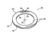
- FIG. 2is a perspective view of a quartz ring having a laser annealed surface
- FIGS. 3A and 3Bare optical microscopy images of a quartz surface with surface microcracks before and after laser treatment, respectively;
- FIG. 4is a schematic view of a laser annealing apparatus suitable for localized surface annealing of the chamber component
- FIG. 5is a sectional schematic view of a substrate processing chamber that uses the ring of FIG. 2 ;
- FIG. 6is a schematic partial sectional side view of support assembly that uses the ring of FIG. 2 in the chamber of FIG. 5 .
- a substrate processing chamber component 20comprises a structural body 24 with localized surface regions 26 having microcracks 28 , as shown in FIGS. 1A to 1D .
- the chamber component 20can be made from a ceramic, glass or glass ceramic material, such as for example, quartz, silica glass, aluminum oxide, titanium oxide, silicon nitride, zirconium oxide, and other such materials.
- the surface microcracks 28are caused by fine dust or other abrasive materials that strike and abrade the component surface 26 during or after fabrication of the component.
- FIG. 1Ashows a component 20 made from glass, which is amorphous and has short range atomic order but no long range atomic order.
- silica glasshas short range order within individual silica tetrahedrons with fixed silicon and oxygen bond angles, but the silica tetrahedral may be interconnected with random bond angles.
- the microcracksare very fine and terminate with atomic bonds.
- Microcrystalline ceramic materialsas shown in FIG. 1C , are polycrystalline with fine grains 29 having micron sized dimensions.
- the microcracks 28typically extend around the fine grains 29 and or along grain boundaries 31 , but they can also cut across single or adjacent grains 29 .
- the surface microcracks 28 on the components 20serve as stress concentrators that cause applied forces to concentrate on the tips of the microcracks 20 .
- microcracks 28are very small, on the level of atomic bonds between atoms of the component material in glass materials, and on the level of micron sized grains in microcrystalline materials, the applied stress is magnified tremendously at the crack tip. This results in rapid catastrophic failure modes in which a portion of the component 20 can easily crack or chip away with even a small applied force or impact.
- the component 20comprises a structural body 24 that is shaped as a ring 25 , as schematically illustrated in FIG. 2 .
- the ring 25comprises the surface 26 having the microcracks 28 .
- the ring 25is annular with an internal sidewall 28 and an external sidewall 30 .
- the internal sidewall 28faces an internal axis 34 about which the structural body has rotational symmetry.
- the ring 25is shaped to protect or conform to a section of a processing chamber, chamber component, or substrate within the chamber.
- the component 20can be a liner or shield that is a cylindrical member which is sized to fit around a substrate being processed in a chamber.
- the shield 20can be a rig of quartz that surrounds the substrate.
- the component 20can also be a deposition ring, shadow ring or cover ring.
- Yet other chamber componentscomprise chamber wall liners.
- the surface microcracks 28 on the structural body 24 of the component 20are annealed to heal and close off the microcracks as shown in FIGS. 1B and 1D , to reduce crack propagation and increase the fracture resistance of the component 20 .
- a laser beamis directed onto the localized surface regions 26 of the component 20 at a sufficiently high intensity and for a sufficient time to cause the region 26 about the microcracks 28 to soften and heal the microcracks 28 .
- the laser beamis used to selectively heat the localized surface regions of the component 20 .
- the localized surface regions 26are those that are prone to fracture during use, or which have excessive microcracks during fabrication, for example, regions which are more readily subject to abrasion and grinding from applied external forces during the handling of manufacture of the component.
- the localized surface regionsmay be on the flat top surface of the ring 25 .
- the localized surface regions 26can also include those regions of the component 20 which are more susceptible to applied stresses during handling and use.
- the edges 36 of the quartz rings 25 used in the chamber 20are often chipped or cracked when the ring 25 is removed for cleaning or replacing after use for a predetermined number of process cycles.
- the edges 36which may also include corners 40 , are often easily cracked or chipped in use.
- increasing the fracture strength of the regions 26 of the quartz ringcan significantly increase its process lifetime.
- the energy of the laser beam and beam characteristicsmay be controlled to selectively heat a shallow portion of the localized surface region of the component 20 above the microcrack healing temperature needed for annealing the surface microcracks 28 .
- a laser beamis used to heat a thin surface layer having a depth of less than 500 microns, and more typically less the 100 microns, of the localized surface regions 26 of a component 20 .
- the focused laser beamselectively heats the localized surface regions 26 of the component 20 to a temperature above the crack healing temperature without excessively raising the bulk temperature of the component, which may result in distortion or thermal fracture of the component 20 .
- a laser beam heat treatmentis described as an exemplary annealing process
- other annealing processescan also be used.
- alternative annealing processesinclude plasma jet heating, electrical arc heating, flame heating.
- the scope of the present inventionshould not be limited to the exemplary versions described herein, and the invention includes other localized surface annealing processes and apparatus as would be apparent to those of ordinary skill in the art.
- the microcrack formation processis essentially partially or entirely reversed by the annealing step.
- the localized heat energy supplied to the microcracked surface by the lasercauses softening and fluxing of the localized heated region causing the microcracks 28 to close and seal themselves off, as schematically shown in FIGS. 1B and 1D .
- FIGS. 1A and 1Bit is believed that in amorphous or glassy materials, as shown in FIGS. 1A and 1B , the microcrack healing process is enhanced because atomic forces acting across the tips of the microcracks 28 tend to pull crack surfaces back into contact across the entire microcrack plane.
- the grain boundary regions 31often contain small amounts of impurities that act as fluxing agents causing more rapid fluxing and resultant healing of the microcrack surfaces.
- FIGS. 3A and 3Bare optical microscopy images of a quartz surface comprising surface microcracks before and after laser treatment, respectively.
- FIG. 3Ashows the quartz surface with a large number of microcracks corresponding to the dark lines between the lighter grain surface regions.
- FIG. 3Bwhich is a photo of the laser treated sample, it is seen that most of the surface microcracks have disappeared to provide a smooth and continuous surface.
- an indentation markwas artificially made at the center of the quartz specimen.
- the size of the indentation markwas on the order of the surface roughness of the quartz material, consequently, it is not visible in the original, un-treated quartz material shown in FIG. 3A .
- the partially healed indentation markis visible as a faint dark spot in the photo of the laser treated sample of FIG. 3B , because the surface of the laser treated specimen is smooth and absent surface microcracks and roughness.
- Annealing of surface microcracks of the chamber componentswas also found to substantially increase hardness and fracture stress of the annealed material, which would significantly improve its resistance to chipping and cracking.
- an increasing loadwas applied normal to the plane of the specimen surface using a micro-indenter having a known geometrical shape. The load is then reduced until the surface of the specimen partially or completely relaxes, and a depth of indentation is then measured. The load is then progressively increased and the indentation and measurement process repeated until hardness is compromised and the specimen cracks.
- the hardnesswas measured using a Nano Hardness Tester. The load applied was on the order of a nano Newton and the displacement was accurately determined using a differential capacitor sensor. Both an original untreated quartz specimen and a laser annealed quartz specimen were measured. The mean Vickers hardness index for the untreated specimen was about 771.68, and the Vickers hardness index for the laser annealed quartz specimen had a mean of 951.68. Thus, the laser annealed quartz specimen had a Vickers hardness which was at least about 10%, and more preferably at least about 25% harder than the untreated specimen.
- Another measurement demonstrating increased crack and chip resistanceis a fracture stress measurement. Ceramic materials are often tested in a flexural or bending test instead of tensile test because of their brittle nature. The stress at which the ceramic material fails by fracture is called the fracture stress or fracture strength of the material.
- the mean fracture stress of the untreated quartz specimenswas 86.23 MPa and the mean fracture stress of the laser annealing quartz specimen was 132.27 MPa.
- the mean fracture stress of the laser annealed quartz specimenwas at least about 25%, and more preferably, at least about 50% higher than that of the untreated specimen.
- annealing of the microcracks 28 in localized surface regions 26 of a component 20can significantly increase the surface smoothness, hardness, and fracture strength of the component 20 . Absence or reduction of microcracks 28 in the surface of the component 20 , especially in regions which are susceptible to applied stresses or are simply more fragile, such as projections, corners 40 and edges of the component, substantially increases the crack and chip resistance of the component 20 .
- surface annealingallows healing and increased strength of selected surface regions 26 without subjecting the entire component 20 to elevated temperatures that may cause structural deformation or other thermal degradation. However, the entire component may also be annealed by suitable heat treatment.
- the laser annealing apparatus 50comprises a laser beam enclosure 52 that encloses a laser beam source 54 powered by a power supply 55 .
- Suitable laser beam sources 54 that can be used for microcrack annealinginclude, for example, Ar (argon), CO 2 and KrF lasers.
- An argon lasertransmits in the visible wavelength at about 5145 angstroms.
- a CO 2 laseris an infra-red energy source having a wavelength of 10.6 ⁇ m, and can provide beams having a power of the order of 10 kilowatts.
- the CO 2 laseris 100 ⁇ more efficient than the argon laser and is of greater intensity, allowing much faster scan speeds and larger spot sizes than the argon laser.
- a CO 2 laseris described in U.S. Pat. No. 3,702,973 issued on Nov. 14, 1972, which is incorporated herein in its entirety.
- Yet another type of laseris a KrF excimer laser having a wavelength of about 248 nm, an Eg of 5.0 eV, an efficiency of about 3%, and an output energy of 350 mJ.
- the laser beamis typically a circular beam having a beam diameter of typically less than about 10 mm, and more typically from about 0.5 mm to about 4 mm.
- suitable laser beamscan have wavelengths of from about 190 nm to about 10,600 nm.
- the laseris typically operated at a power level of from about 5 Watts to about 10,000 Watts.
- the laser 50produces a laser beam 56 that is focused at a primary focal point 58 and is re-imaged by a refocusing mirror 62 which provides a larger focal length, to a secondary focal point 84 .
- a dithering mirror 68which is connected to a dithering drive motor 72 which vibrates the dithering mirror 68 at a preselected frequency.
- the dithering drive motor 72vibrates the dithering mirror 68 about an axis 76 substantially in the plane of the mirror 68 and transverse to the incident laser beam 56 focused by mirror.
- the dithered beam emanating from the dithering mirror 68spacially oscillates an arc line which is transverse to the plane of the drawing in FIG. 1 .
- the laser beam 56has an intensity distribution across the beam diameter, also called the intensity profile or intensity shape of the beam, which depends on the type of laser 50 .
- a common beam profile shapeis a Gaussian shape, and more typically a U-shaped intensity profile. Focusing of the laser beam changes the cross-sectional size of the beam but not its beam intensity distribution which remains Gaussian or U-shaped.
- One method of correcting for the Gaussian or U-shaped cross-section of the laser beamis to spacially oscillate the laser beam 56 , also known as dithering.
- the spacial oscillation of the laser beam 56may be sinusoidal, sawtooth or square waves.
- Spacial oscillation or dithering of the laser beam 56produces an average and more uniform intensity of radiation across the region scanned by the dithering beam.
- the laser beam 56has an approximate Gaussian distribution at its focal point and the spacial oscillation or dithering is sinusoidal.
- the ditheringis produced by the dithering mirror 76 which oscillates back and forth on the axis 76 that is parallel to the plane of the mirror 76 and transverse to the plane of the dither.
- the dithered beamcovers an area that at least twice as large as the undithered beam.
- the average intensity at each point across the dithering beam projected on the localized surface regionis approximately flat in the center region and with peaks at the opposite ends.
- the resulting intensity profile of the dithering beamis shaped like a square wave and provides a good intensity profile for scanning across the localized surface region in contiguous, overlapping sweeps. however, other beam shapes, such as sine wave shapes, can also be used with appropriately compensating laser scanning methods.
- the dithered beamthen passes through a beam width controlling aperture 80 having a controllable or predefined fixed aperture 82 at the second focal point 84 .
- the aperture 80is located between the dithering mirror 76 and a second focusing system 90 which may be a scanning mirror or lens.
- the axis 76 of mirror 68may be transverse or parallel to the plane of the drawing in FIG. 1 .
- the beamis then projected onto a scanning mirror 92 driven by a scanning system 94 .
- the scanning system 94oscillates the mirror 92 on its axis 96 to sweep and scan the beam 56 back and forth over a selected localized region 100 on the chamber component being treated.
- the scanned beampasses through a window 102 in the enclosure 100 .
- the sweep rate of scanning mirror 92is typically slower than the dither frequency of the dithering mirror 68 .
- a focused CO 2 laser having a beam diameter of about 500 ⁇ mmay be scanned at from about 1 mm/sec to about 100 mm/sec.
- the scanning systemcommunicates with an X-Y movable stage 110 which is driven by a stage motor 114 .
- the stage 110can also be adapted to slide in the Z or vertical direction to change the beam width incident on the component.
- the scanning system 94synchronizes the sweep rate of the scanning mirror 92 with the movement of the stage 110 , and consequently, the movement of the chamber component resting on the stage 110 , to uniformly scan the dithered and apertured beam across the component.
- the scanning parametersare selected to uniformly heat the localized surface region across which the beam is being scanned, by adjusting the scanning speed and pattern to compensate for the shape of the laser beam.
- the intensity distribution of the beam 56can contain rings around a central maximum and even a depression in the middle of the beam due to near field annular characteristics of the beam. Furthermore, it is also desirable to overlap the beam scans to compensate for any variation in the cross-sectional intensity of a laser beam—if the laser beam sweeps across the surface in raster-type scans without overlapping of beam scans, the depth of heat treatment may vary across the beam scan depending on the shape of the beam.
- the laser beam annealing apparatus 50further comprises a controller 118 which controls operation of the system and is connected to the power supply 55 , which powers the laser 54 , the dithering drive motor 72 , and the scanning system 94 .
- the controller 118accepts input from a user input device 120 and displays input parameters, and scanning system information on a display 122 .
- the controller 118can be a conventional computer having a central processing unit (CPU) connected to suitable memory devices, including random access memory and storage memory on disk drives, and interface cards and buses.
- the laser beam annealing apparatus 50is capable of laser annealing localized surface regions across the component surface with good uniformity over the entire surface region.
- a component 20 that is annealed to reduce or heal microcrackscan be used in a substrate processing apparatus 200 , as schematically illustrated in FIG. 5 , which is used to fabricate substrates 215 , such as semiconductor wafers and displays.
- the apparatus 200can be a MxP, MxP Super E, or eMax type etching chamber, which are from Applied Materials Inc., Santa Clara, Calif., and are generally described in commonly assigned U.S. Pat. Nos. 4,842,683 and 5,215,619 to Cheng et al; and U.S. Pat. No. 4,668,338 to Maydan et al, all of which are incorporated herein by reference in their entireties.
- An exemplary apparatus 200may be used in a multi-chamber integrated system for processing semiconductor substrates as described in U.S. Pat. No. 4,951,601 to Maydan et al, which is also incorporated herein by reference in its entirety.
- the apparatus 200comprises a process chamber 225 and ancillary control, electrical, plumbing and support components.
- a support assembly 230comprising a support 238 is provided to receive the substrate 215 in a process zone 235 .
- the support 238may be an electrostatic chuck 240 comprising a dielectric 45 at least partially covering an electrode 250 , and having gas outlets 260 through which a heat transfer gas, such as helium, may be passed from a heat transfer gas source 265 via gas conduits 270 , to control the temperature of the substrate 215 .
- the support 238may be a vacuum or mechanical chuck or any other support as is known in the art.
- the electrode 250is electrically charged by an electrode voltage supply 275 to electrostatically hold the substrate 215 .
- a base 280 below the electrostatic chuck 240may optionally contain a heat exchanger, such as channels through which a heat transfer fluid may be circulated.
- Process gasis introduced into the chamber 225 through a gas supply 285 that includes a gas source 290 and one or more gas nozzles 295 terminating in the chamber 225 .
- the gas nozzles 295may be located around the periphery of the substrate 215 (as shown) or in a showerhead mounted on the ceiling of the chamber (not shown).
- a gas flow controller 300is used to control the flow rate of the process gas.
- Spent process gas and byproductsare exhausted from the chamber 225 through an exhaust system 305 .
- the exhaust system 305typically comprises an exhaust conduit leading to a plurality of pumps, such as roughing or high vacuum pumps, that evacuate the gas in the chamber 225 .
- a throttle valve 310is provided in the exhaust conduit to control the pressure of the gas in the chamber 225 .
- An energized gassuch as for example a gaseous plasma, is generated from the process gas by a gas energizer 275 that couples electromagnetic energy, such as RF or microwave energy, to the process gas in the process zone 235 of the chamber 225 .
- the gas energizer 275may comprise a first process electrode 315 such as an electrically grounded sidewall or ceiling of the chamber and a second electrode which may be the electrode 250 in dielectric 245 .
- the first and second electrodes 315 , 250are electrically biased relative to one another by an RF voltage provided by an electrode voltage supply 275 .
- the frequency of the RF voltage applied to the electrodes 315 , 250is typically from about 50 KHz to about 60 MHz.
- the gas energizer 275may also or alternatively include an inductor antenna (not shown) comprising one or more coils to inductively couple RF energy to the chamber 225 .
- the capacitively generated plasmamay be enhanced by electron cyclotron resonance in a magnetically enhanced reactor in which a magnetic field generator 320 , such as a permanent magnet or electromagnetic coils, provides a magnetic field in the chamber 225 that has a rotating magnetic field having an axis that rotates parallel to the plane of the substrate 215 .
- the chamber 225may also comprise one or more process monitoring systems (not shown) to monitor the processes being performed on the substrate 215 .
- a typical process monitoring systemcomprises an interferometric system that measures an intensity of light reflected from a layer being processed on the substrate 215 , or a plasma emission analysis system that measures a change in light emission intensity of a gas species in the chamber 225 .
- the process monitoring systemis useful to detect an endpoint of a process being performed on the substrate 215 .
- the laser annealed component 20such as the ring 25 is fitted around the substrate support 238 of the support assembly 230 in the chamber 225 .
- the ring 25may protect the support assembly 230 , for example, the dielectric 245 of the electrostatic chuck 240 from erosion by preventing contact of the dielectric 245 with the energized process gas in the chamber 225 .
- the ring 25may have other uses in the support assembly 230 .
- additional structuressuch as the collar 210 which surrounds the ring 25 can also be laser annealed to reduce surface microcracks.
- the collar 210can be made from a ceramic material such as aluminum oxide or silicon oxide.
- the collar 210may serve as a shield, which together with the ring form a replaceable process kit for the chamber.
- Other annular structuressuch as chamber wall liners can also be laser annealed, and can also be part of the process kit for the chamber 225 .
- the annealed chamber component 20can be from chamber components such as the ceiling or walls of the chamber 225 .
- alternative methods of surface annealingcan also be used.
- relative or positional terms shown with respect to the exemplary embodimentsare interchangeable. Therefore, the appended claims should not be limited to the descriptions of the preferred versions, materials, or spatial arrangements described herein to illustrate the invention.
Landscapes
- Engineering & Computer Science (AREA)
- Chemical & Material Sciences (AREA)
- Physics & Mathematics (AREA)
- Power Engineering (AREA)
- Condensed Matter Physics & Semiconductors (AREA)
- General Physics & Mathematics (AREA)
- Manufacturing & Machinery (AREA)
- Computer Hardware Design (AREA)
- Microelectronics & Electronic Packaging (AREA)
- Ceramic Engineering (AREA)
- Materials Engineering (AREA)
- Organic Chemistry (AREA)
- Optics & Photonics (AREA)
- Structural Engineering (AREA)
- Health & Medical Sciences (AREA)
- Toxicology (AREA)
- Plasma & Fusion (AREA)
- Mechanical Engineering (AREA)
- Recrystallisation Techniques (AREA)
- Crystals, And After-Treatments Of Crystals (AREA)
- Container, Conveyance, Adherence, Positioning, Of Wafer (AREA)
- Physical Or Chemical Processes And Apparatus (AREA)
- Re-Forming, After-Treatment, Cutting And Transporting Of Glass Products (AREA)
- Drying Of Semiconductors (AREA)
Abstract
Description
Claims (32)
Priority Applications (8)
| Application Number | Priority Date | Filing Date | Title |
|---|---|---|---|
| US11/181,041US8617672B2 (en) | 2005-07-13 | 2005-07-13 | Localized surface annealing of components for substrate processing chambers |
| JP2008521576AJP2009501452A (en) | 2005-07-13 | 2006-07-12 | Local surface annealing of components for substrate processing chambers |
| KR1020077030395AKR101278217B1 (en) | 2005-07-13 | 2006-07-12 | Localized surface annealing of components for substrate processing chambers |
| EP06787040.2AEP1902003B1 (en) | 2005-07-13 | 2006-07-12 | Localized surface annealing of components for substrate processing chambers |
| PCT/US2006/027078WO2007008999A2 (en) | 2005-07-13 | 2006-07-12 | Localized surface annealing of components for substrate processing chambers |
| CN2006800252684ACN101218191B (en) | 2005-07-13 | 2006-07-12 | Localized surface annealing of components for substrate processing chambers |
| TW095125734ATWI417961B (en) | 2005-07-13 | 2006-07-13 | Localized surface annealing of components for substrate processing chambers |
| US14/088,216US9481608B2 (en) | 2005-07-13 | 2013-11-22 | Surface annealing of components for substrate processing chambers |
Applications Claiming Priority (1)
| Application Number | Priority Date | Filing Date | Title |
|---|---|---|---|
| US11/181,041US8617672B2 (en) | 2005-07-13 | 2005-07-13 | Localized surface annealing of components for substrate processing chambers |
Related Child Applications (1)
| Application Number | Title | Priority Date | Filing Date |
|---|---|---|---|
| US14/088,216DivisionUS9481608B2 (en) | 2005-07-13 | 2013-11-22 | Surface annealing of components for substrate processing chambers |
Publications (2)
| Publication Number | Publication Date |
|---|---|
| US20070014949A1 US20070014949A1 (en) | 2007-01-18 |
| US8617672B2true US8617672B2 (en) | 2013-12-31 |
Family
ID=37637934
Family Applications (2)
| Application Number | Title | Priority Date | Filing Date |
|---|---|---|---|
| US11/181,041Expired - Fee RelatedUS8617672B2 (en) | 2005-07-13 | 2005-07-13 | Localized surface annealing of components for substrate processing chambers |
| US14/088,216Active2027-01-17US9481608B2 (en) | 2005-07-13 | 2013-11-22 | Surface annealing of components for substrate processing chambers |
Family Applications After (1)
| Application Number | Title | Priority Date | Filing Date |
|---|---|---|---|
| US14/088,216Active2027-01-17US9481608B2 (en) | 2005-07-13 | 2013-11-22 | Surface annealing of components for substrate processing chambers |
Country Status (7)
| Country | Link |
|---|---|
| US (2) | US8617672B2 (en) |
| EP (1) | EP1902003B1 (en) |
| JP (1) | JP2009501452A (en) |
| KR (1) | KR101278217B1 (en) |
| CN (1) | CN101218191B (en) |
| TW (1) | TWI417961B (en) |
| WO (1) | WO2007008999A2 (en) |
Cited By (16)
| Publication number | Priority date | Publication date | Assignee | Title |
|---|---|---|---|---|
| USD711331S1 (en)* | 2013-11-07 | 2014-08-19 | Applied Materials, Inc. | Upper chamber liner |
| USD741823S1 (en)* | 2013-07-10 | 2015-10-27 | Hitachi Kokusai Electric Inc. | Vaporizer for substrate processing apparatus |
| US20170162422A1 (en)* | 2015-12-07 | 2017-06-08 | Applied Materials, Inc. | Amalgamated cover ring |
| WO2017172884A1 (en)* | 2016-03-31 | 2017-10-05 | Tronox Llc | Centrifugal aluminum chloride generator |
| USD875053S1 (en)* | 2017-04-28 | 2020-02-11 | Applied Materials, Inc. | Plasma connector liner |
| USD875055S1 (en)* | 2017-04-28 | 2020-02-11 | Applied Materials, Inc. | Plasma connector liner |
| USD875054S1 (en)* | 2017-04-28 | 2020-02-11 | Applied Materials, Inc. | Plasma connector liner |
| US10857625B2 (en) | 2016-10-14 | 2020-12-08 | Applied Materials, Inc. | Texturizing a surface without bead blasting |
| USD925481S1 (en)* | 2018-12-06 | 2021-07-20 | Kokusai Electric Corporation | Inlet liner for substrate processing apparatus |
| US20220305586A1 (en)* | 2021-03-26 | 2022-09-29 | Samsung Display Co., Ltd. | Laser defect removal apparatus and window defect removal method |
| US11955361B2 (en) | 2021-04-15 | 2024-04-09 | Applied Materials, Inc. | Electrostatic chuck with mesas |
| USD1042374S1 (en) | 2022-03-18 | 2024-09-17 | Applied Materials, Inc. | Support pipe for an interlocking process kit for a substrate processing chamber |
| USD1042373S1 (en) | 2022-03-18 | 2024-09-17 | Applied Materials, Inc. | Sliding ring for an interlocking process kit for a substrate processing chamber |
| USD1049067S1 (en)* | 2022-04-04 | 2024-10-29 | Applied Materials, Inc. | Ring for an anti-rotation process kit for a substrate processing chamber |
| USD1055006S1 (en)* | 2022-03-18 | 2024-12-24 | Applied Materials, Inc. | Support ring for an interlocking process kit for a substrate processing chamber |
| USD1066275S1 (en) | 2022-04-04 | 2025-03-11 | Applied Materials, Inc. | Baffle for anti-rotation process kit for substrate processing chamber |
Families Citing this family (17)
| Publication number | Priority date | Publication date | Assignee | Title |
|---|---|---|---|---|
| US20080264564A1 (en) | 2007-04-27 | 2008-10-30 | Applied Materials, Inc. | Method of reducing the erosion rate of semiconductor processing apparatus exposed to halogen-containing plasmas |
| JP4286025B2 (en)* | 2003-03-03 | 2009-06-24 | 川崎マイクロエレクトロニクス株式会社 | Method of reclaiming quartz jig, method of reusing and using semiconductor device |
| US8617672B2 (en) | 2005-07-13 | 2013-12-31 | Applied Materials, Inc. | Localized surface annealing of components for substrate processing chambers |
| US10622194B2 (en) | 2007-04-27 | 2020-04-14 | Applied Materials, Inc. | Bulk sintered solid solution ceramic which exhibits fracture toughness and halogen plasma resistance |
| TWI744898B (en)* | 2007-04-27 | 2021-11-01 | 美商應用材料股份有限公司 | Method and apparatus which reduce the erosion rate of surfaces exposed to halogen-containing plasmas |
| US10242888B2 (en) | 2007-04-27 | 2019-03-26 | Applied Materials, Inc. | Semiconductor processing apparatus with a ceramic-comprising surface which exhibits fracture toughness and halogen plasma resistance |
| US8291728B2 (en)* | 2009-02-27 | 2012-10-23 | Corning Incorporated | Method for the joining of low expansion glass |
| DK2773596T3 (en)* | 2011-11-02 | 2020-09-14 | Ferro Corp | MICROWAVE SEALING OF INORGANIC SUBSTRATES USING LOW MELTING GLASS SYSTEMS |
| KR101991405B1 (en)* | 2012-09-19 | 2019-06-20 | 삼성전자주식회사 | Beam shaper, a laser annealing system with the same, and method of fabricating a reflective photomask using this system |
| US9142465B1 (en) | 2013-03-13 | 2015-09-22 | Sandia Corporation | Precise annealing of focal plane arrays for optical detection |
| US9653341B2 (en)* | 2014-03-05 | 2017-05-16 | Taiwan Semiconductor Manufacturing Company Ltd. | Semiconductor structure and manufacturing method thereof |
| US10126061B1 (en)* | 2014-08-28 | 2018-11-13 | Apple Inc. | Localized strengthening of features for a sapphire component |
| US10422028B2 (en)* | 2015-12-07 | 2019-09-24 | Lam Research Corporation | Surface coating treatment |
| DE102017101808B4 (en)* | 2016-02-04 | 2024-12-24 | Schott Ag | Method for checking the thickness of a substrate |
| US10593602B2 (en)* | 2018-04-27 | 2020-03-17 | Semiconductor Components Industries, Llc | Semiconductor substrate crack mitigation systems and related methods |
| CN112195317B (en)* | 2020-10-15 | 2022-04-15 | 温州大学 | A cold-rolled composite laser surface annealing process method for a heterogeneous structure high-entropy alloy |
| US12434999B2 (en) | 2022-11-15 | 2025-10-07 | Communications Test Design, Inc. | System and method for removing defects from glass materials with laser irradiation |
Citations (389)
| Publication number | Priority date | Publication date | Assignee | Title |
|---|---|---|---|---|
| US2705500A (en) | 1953-11-04 | 1955-04-05 | Leon L Deer | Cleaning aluminum |
| US3117883A (en) | 1960-09-23 | 1964-01-14 | Glidden Co | Pigment for aqueous latex emulsion paints |
| US3457151A (en) | 1966-10-27 | 1969-07-22 | Solutec Corp | Electrolytic cleaning method |
| US3482082A (en) | 1966-03-18 | 1969-12-02 | Techicon Corp | Sample identification apparatus |
| US3522083A (en) | 1967-11-03 | 1970-07-28 | Grace W R & Co | Phosphonitrilic laminating and molding resins |
| US3565771A (en) | 1967-10-16 | 1971-02-23 | Shipley Co | Etching and metal plating silicon containing aluminum alloys |
| US3679460A (en) | 1970-10-08 | 1972-07-25 | Union Carbide Corp | Composite wear resistant material and method of making same |
| US3843472A (en)* | 1971-05-21 | 1974-10-22 | Glaverbel | Method of strengthening an edge of a glass article and article with strengthened edge |
| US3848104A (en) | 1973-04-09 | 1974-11-12 | Avco Everett Res Lab Inc | Apparatus for heat treating a surface |
| GB1424365A (en) | 1972-05-25 | 1976-02-11 | Messerschmitt Boelkow Blohm | Method for producing predetermined wall thickness changes in rotationally symmetrical hollow bodies |
| US4358659A (en) | 1981-07-13 | 1982-11-09 | Mostek Corporation | Method and apparatus for focusing a laser beam on an integrated circuit |
| USRE31198E (en) | 1974-02-14 | 1983-04-05 | Amchem Products, Inc. | Method for cleaning aluminum at low temperatures |
| US4412133A (en) | 1982-01-05 | 1983-10-25 | The Perkin-Elmer Corp. | Electrostatic cassette |
| US4419201A (en) | 1981-08-24 | 1983-12-06 | Bell Telephone Laboratories, Incorporated | Apparatus and method for plasma-assisted etching of wafers |
| US4430360A (en) | 1981-03-11 | 1984-02-07 | The United States Of America As Represented By The Administrator Of The National Aeronautics And Space Administration | Method of fabricating an abradable gas path seal |
| US4480284A (en) | 1982-02-03 | 1984-10-30 | Tokyo Shibaura Denki Kabushiki Kaisha | Electrostatic chuck plate |
| US4491496A (en) | 1983-01-05 | 1985-01-01 | Commissariat A L'energie Atomique | Enclosure for the treatment, and particularly for the etching of substrates by the reactive plasma method |
| FR2562097A1 (en) | 1984-03-28 | 1985-10-04 | Andritz Ag Maschf | Process for pickling alloy steels, copper, alloys of non-ferrous heavy metals, titanium, zirconium, tantalum and the like by means of nitric acid baths |
| US4606802A (en) | 1983-12-21 | 1986-08-19 | Hitachi, Ltd. | Planar magnetron sputtering with modified field configuration |
| US4643950A (en)* | 1985-05-09 | 1987-02-17 | Agency Of Industrial Science And Technology | Semiconductor device |
| US4645218A (en) | 1984-07-31 | 1987-02-24 | Kabushiki Kaisha Tokuda Seisakusho | Electrostatic chuck |
| US4665463A (en) | 1983-09-30 | 1987-05-12 | U.S. Philips Corporation | Electrostatic chuck |
| US4673554A (en) | 1984-12-18 | 1987-06-16 | Sumitomo Chemical Company, Limited | Method of purifying tantalum |
| US4713119A (en) | 1986-03-20 | 1987-12-15 | Stauffer Chemical Company | Process for removing alkali metal aluminum silicate scale deposits from surfaces of chemical process equipment |
| US4717462A (en) | 1985-10-25 | 1988-01-05 | Hitachi, Ltd. | Sputtering apparatus |
| US4732792A (en) | 1984-10-08 | 1988-03-22 | Canon Kabushiki Kaisha | Method for treating surface of construction material for vacuum apparatus, and the material treated thereby and vacuum treatment apparatus having the treated material |
| US4756322A (en) | 1985-03-08 | 1988-07-12 | Lami Philippe A | Means for restoring the initial cleanness conditions in a quartz tube used as a reaction chamber for the production of integrated circuits |
| US4814575A (en) | 1986-10-16 | 1989-03-21 | Compagnie Generale D'electricite | Method of surface-treating ceramic workpieces using a laser |
| US4832781A (en) | 1988-01-07 | 1989-05-23 | Varian Associates, Inc. | Methods and apparatus for thermal transfer with a semiconductor wafer in vacuum |
| US4872250A (en) | 1986-09-18 | 1989-10-10 | Ernst Grob Ag | Method for fabricating a dished hollow body possessing a linear or helical inner toothing |
| US4913784A (en) | 1985-07-04 | 1990-04-03 | Licentia Patent-Verwaltungs Gmbh | Process for metallizing a ceramic substrate |
| US4959105A (en) | 1988-09-30 | 1990-09-25 | Fred Neidiffer | Aluminium cleaning composition and process |
| US4995958A (en) | 1989-05-22 | 1991-02-26 | Varian Associates, Inc. | Sputtering apparatus with a rotating magnet array having a geometry for specified target erosion profile |
| US4996859A (en) | 1989-10-23 | 1991-03-05 | A. J. Rose Manufacturing Company | Method and apparatus for roll forming metal |
| US5009966A (en) | 1987-12-31 | 1991-04-23 | Diwakar Garg | Hard outer coatings deposited on titanium or titanium alloys |
| US5032469A (en) | 1988-09-06 | 1991-07-16 | Battelle Memorial Institute | Metal alloy coatings and methods for applying |
| US5035787A (en) | 1987-07-22 | 1991-07-30 | Microbeam, Inc. | Method for repairing semiconductor masks and reticles |
| US5055964A (en) | 1990-09-07 | 1991-10-08 | International Business Machines Corporation | Electrostatic chuck having tapered electrodes |
| US5064511A (en) | 1989-06-05 | 1991-11-12 | Diaprint S.R.L. | Electrochemical graining of aluminum or aluminum alloy surfaces |
| US5104501A (en) | 1989-06-13 | 1992-04-14 | Daicel Chemical Industries, Ltd. | Electrolytic cleaning method and electrolytic cleaning solution for stamper |
| US5104834A (en) | 1988-04-26 | 1992-04-14 | Tot Ltd. | Dielectric ceramics for electrostatic chucks and method of making them |
| US5117121A (en) | 1989-04-25 | 1992-05-26 | Toto Ltd. | Method of and apparatus for applying voltage to electrostatic chuck |
| EP0239349B1 (en) | 1986-03-24 | 1992-07-01 | Conoco Inc. | Improved method for applying protective coatings |
| US5151845A (en) | 1988-09-19 | 1992-09-29 | Toto Ltd. | Electrostatic chuck |
| US5164016A (en) | 1990-02-08 | 1992-11-17 | Ugine, Aciers De Chatillon Et Gueugnon | Method for pickling or cleaning materials of steel, in particular stainless steel |
| US5166856A (en) | 1991-01-31 | 1992-11-24 | International Business Machines Corporation | Electrostatic chuck with diamond coating |
| US5180322A (en) | 1990-08-22 | 1993-01-19 | Dainippon Screen Mfg. Co., Ltd. | Manufacturing process of shadow mask and shadow mask plate therefor |
| US5180563A (en) | 1989-10-24 | 1993-01-19 | Gte Products Corporation | Treatment of industrial wastes |
| US5191506A (en) | 1991-05-02 | 1993-03-02 | International Business Machines Corporation | Ceramic electrostatic chuck |
| US5202008A (en) | 1990-03-02 | 1993-04-13 | Applied Materials, Inc. | Method for preparing a shield to reduce particles in a physical vapor deposition chamber |
| US5215624A (en) | 1991-02-08 | 1993-06-01 | Aluminum Company Of America | Milling solution and method |
| US5215639A (en) | 1984-10-09 | 1993-06-01 | Genus, Inc. | Composite sputtering target structures and process for producing such structures |
| US5242706A (en)* | 1991-07-31 | 1993-09-07 | The United States Of America As Represented By The Secretary Of The Navy | Laser-deposited biocompatible films and methods and apparatuses for producing same |
| US5248386A (en) | 1991-02-08 | 1993-09-28 | Aluminum Company Of America | Milling solution and method |
| US5258047A (en) | 1990-11-30 | 1993-11-02 | Hitachi, Ltd. | Holder device and semiconductor producing apparatus having same |
| US5270266A (en) | 1991-12-13 | 1993-12-14 | Tokyo Electron Limited | Method of adjusting the temperature of a semiconductor wafer |
| US5275683A (en) | 1991-10-24 | 1994-01-04 | Tokyo Electron Limited | Mount for supporting substrates and plasma processing apparatus using the same |
| US5280156A (en) | 1990-12-25 | 1994-01-18 | Ngk Insulators, Ltd. | Wafer heating apparatus and with ceramic substrate and dielectric layer having electrostatic chucking means |
| US5292554A (en) | 1992-11-12 | 1994-03-08 | Applied Materials, Inc. | Deposition apparatus using a perforated pumping plate |
| US5304248A (en) | 1990-12-05 | 1994-04-19 | Applied Materials, Inc. | Passive shield for CVD wafer processing which provides frontside edge exclusion and prevents backside depositions |
| US5314597A (en) | 1992-03-20 | 1994-05-24 | Varian Associates, Inc. | Sputtering apparatus with a magnet array having a geometry for a specified target erosion profile |
| US5315473A (en) | 1992-01-21 | 1994-05-24 | Applied Materials, Inc. | Isolated electrostatic chuck and excitation method |
| US5325261A (en) | 1991-05-17 | 1994-06-28 | Unisearch Limited | Electrostatic chuck with improved release |
| US5324053A (en) | 1992-02-20 | 1994-06-28 | Shin-Etsu Chemical Co., Ltd. | Electrostatic chuck |
| US5338367A (en) | 1989-07-26 | 1994-08-16 | Ugine, Aciers De Chatillon Et Gueugnon | Pickling process in an acid bath of metallic products containing titanium or at least one chemical element of the titanium family |
| EP0610556A1 (en) | 1993-02-09 | 1994-08-17 | Rutgers, The State University | Localized surface glazing of ceramic articles |
| EP0439000B1 (en) | 1990-01-25 | 1994-09-14 | Applied Materials, Inc. | Electrostatic clamp and method |
| US5350479A (en) | 1992-12-02 | 1994-09-27 | Applied Materials, Inc. | Electrostatic chuck for high power plasma processing |
| US5356723A (en) | 1991-12-18 | 1994-10-18 | Sumitomo Metal Industries, Ltd. | Multilayer plated aluminum sheets |
| US5366585A (en)* | 1993-01-28 | 1994-11-22 | Applied Materials, Inc. | Method and apparatus for protection of conductive surfaces in a plasma processing reactor |
| US5382469A (en) | 1992-06-26 | 1995-01-17 | Shin-Etsu Chemical Co., Ltd. | Ceramic-titanium nitride electrostatic chuck |
| EP0635869A1 (en) | 1993-04-22 | 1995-01-25 | Applied Materials, Inc. | Semiconductor processing apparatus, method of making and use of same |
| US5391275A (en) | 1990-03-02 | 1995-02-21 | Applied Materials, Inc. | Method for preparing a shield to reduce particles in a physical vapor deposition chamber |
| US5401319A (en) | 1992-08-27 | 1995-03-28 | Applied Materials, Inc. | Lid and door for a vacuum chamber and pretreatment therefor |
| US5407551A (en) | 1993-07-13 | 1995-04-18 | The Boc Group, Inc. | Planar magnetron sputtering apparatus |
| US5409590A (en) | 1989-04-17 | 1995-04-25 | Materials Research Corporation | Target cooling and support for magnetron sputter coating apparatus |
| US5429711A (en) | 1992-09-18 | 1995-07-04 | Mitsubishi Materials Corporation | Method for manufacturing wafer |
| US5433835A (en) | 1993-11-24 | 1995-07-18 | Applied Materials, Inc. | Sputtering device and target with cover to hold cooling fluid |
| US5458759A (en) | 1991-08-02 | 1995-10-17 | Anelva Corporation | Magnetron sputtering cathode apparatus |
| US5460694A (en) | 1992-06-17 | 1995-10-24 | C.F.P.I. | Process for the treatment of aluminum based substrates for the purpose of anodic oxidation, bath used in said process and concentrate to prepare the bath |
| US5463526A (en) | 1994-01-21 | 1995-10-31 | Lam Research Corporation | Hybrid electrostatic chuck |
| US5474649A (en) | 1994-03-08 | 1995-12-12 | Applied Materials, Inc. | Plasma processing apparatus employing a textured focus ring |
| US5487822A (en) | 1993-11-24 | 1996-01-30 | Applied Materials, Inc. | Integrated sputtering target assembly |
| US5490913A (en) | 1993-05-04 | 1996-02-13 | Balzers Aktiengesellschaft | Magnetic field enhanced sputtering arrangement with vacuum treatment apparatus |
| US5509558A (en) | 1993-07-16 | 1996-04-23 | Kabushiki Kaisha Toshiba | Metal oxide resistor, power resistor, and power circuit breaker |
| US5512078A (en) | 1994-03-24 | 1996-04-30 | Griffin; Stephen E. | Apparatus for making linearly tapered bores in quartz tubing with a controlled laser |
| US5518593A (en) | 1994-04-29 | 1996-05-21 | Applied Komatsu Technology, Inc. | Shield configuration for vacuum chamber |
| US5520740A (en) | 1989-06-28 | 1996-05-28 | Canon Kabushiki Kaisha | Process for continuously forming a large area functional deposited film by microwave PCVD method and apparatus suitable for practicing the same |
| US5531835A (en) | 1994-05-18 | 1996-07-02 | Applied Materials, Inc. | Patterned susceptor to reduce electrostatic force in a CVD chamber |
| US5542559A (en) | 1993-02-16 | 1996-08-06 | Tokyo Electron Kabushiki Kaisha | Plasma treatment apparatus |
| US5549802A (en) | 1993-05-17 | 1996-08-27 | Applied Materials, Inc. | Cleaning of a PVD chamber containing a collimator |
| US5587039A (en) | 1992-01-09 | 1996-12-24 | Varian Associates, Inc. | Plasma etch equipment |
| US5605637A (en) | 1994-12-15 | 1997-02-25 | Applied Materials Inc. | Adjustable dc bias control in a plasma reactor |
| US5614055A (en) | 1993-08-27 | 1997-03-25 | Applied Materials, Inc. | High density plasma CVD and etching reactor |
| US5614071A (en) | 1995-06-28 | 1997-03-25 | Hmt Technology Corporation | Sputtering shield |
| US5643422A (en) | 1994-12-29 | 1997-07-01 | Nec Corporation | Reactive sputtering system for depositing titanium nitride without formation of titanium nitride on titanium target and process of depositing titanium nitride layer |
| US5658442A (en) | 1996-03-07 | 1997-08-19 | Applied Materials, Inc. | Target and dark space shield for a physical vapor deposition system |
| US5660640A (en) | 1995-06-16 | 1997-08-26 | Joray Corporation | Method of removing sputter deposition from components of vacuum deposition equipment |
| US5671835A (en) | 1994-11-07 | 1997-09-30 | Daido Metal Company Ltd. | Wet friction member |
| US5684669A (en) | 1995-06-07 | 1997-11-04 | Applied Materials, Inc. | Method for dechucking a workpiece from an electrostatic chuck |
| US5685914A (en) | 1994-04-05 | 1997-11-11 | Applied Materials, Inc. | Focus ring for semiconductor wafer processing in a plasma reactor |
| US5685959A (en) | 1996-10-25 | 1997-11-11 | Hmt Technology Corporation | Cathode assembly having rotating magnetic-field shunt and method of making magnetic recording media |
| US5690795A (en) | 1995-06-05 | 1997-11-25 | Applied Materials, Inc. | Screwless shield assembly for vacuum processing chambers |
| US5695825A (en) | 1995-05-31 | 1997-12-09 | Amorphous Technologies International | Titanium-containing ferrous hard-facing material source and method for hard facing a substrate |
| US5700179A (en) | 1995-07-28 | 1997-12-23 | Shin-Etsu Handotai Co., Ltd. | Method of manufacturing semiconductor wafers and process of and apparatus for grinding used for the same method of manufacture |
| US5714010A (en) | 1989-06-28 | 1998-02-03 | Canon Kabushiki Kaisha | Process for continuously forming a large area functional deposited film by a microwave PCVD method and an apparatus suitable for practicing the same |
| US5720818A (en) | 1996-04-26 | 1998-02-24 | Applied Materials, Inc. | Conduits for flow of heat transfer fluid to the surface of an electrostatic chuck |
| US5736021A (en) | 1996-07-10 | 1998-04-07 | Applied Materials, Inc. | Electrically floating shield in a plasma reactor |
| US5745331A (en) | 1994-01-31 | 1998-04-28 | Applied Materials, Inc. | Electrostatic chuck with conformal insulator film |
| US5748434A (en) | 1996-06-14 | 1998-05-05 | Applied Materials, Inc. | Shield for an electrostatic chuck |
| US5755887A (en) | 1995-04-06 | 1998-05-26 | Nihon Sinku Gijutsu Kabusiki | Components of apparatus for film making and method for manufacturing the same |
| EP0845545A1 (en) | 1996-11-26 | 1998-06-03 | Applied Materials, Inc. | Coated deposition chamber equipment |
| US5763851A (en) | 1995-11-27 | 1998-06-09 | Applied Materials, Inc. | Slotted RF coil shield for plasma deposition system |
| US5792562A (en) | 1995-01-12 | 1998-08-11 | Applied Materials, Inc. | Electrostatic chuck with polymeric impregnation and method of making |
| US5800686A (en) | 1993-04-05 | 1998-09-01 | Applied Materials, Inc. | Chemical vapor deposition chamber with substrate edge protection |
| US5803977A (en) | 1992-09-30 | 1998-09-08 | Applied Materials, Inc. | Apparatus for full wafer deposition |
| US5808270A (en) | 1997-02-14 | 1998-09-15 | Ford Global Technologies, Inc. | Plasma transferred wire arc thermal spray apparatus and method |
| US5812362A (en) | 1996-06-14 | 1998-09-22 | Applied Materials, Inc. | Method and apparatus for the use of diamond films as dielectric coatings on electrostatic chucks |
| US5810931A (en) | 1996-07-30 | 1998-09-22 | Applied Materials, Inc. | High aspect ratio clamp ring |
| US5821166A (en) | 1996-12-12 | 1998-10-13 | Komatsu Electronic Metals Co., Ltd. | Method of manufacturing semiconductor wafers |
| US5824197A (en) | 1996-06-05 | 1998-10-20 | Applied Materials, Inc. | Shield for a physical vapor deposition chamber |
| US5830327A (en) | 1996-10-02 | 1998-11-03 | Intevac, Inc. | Methods and apparatus for sputtering with rotating magnet sputter sources |
| US5840434A (en) | 1992-09-10 | 1998-11-24 | Hitachi, Ltd. | Thermal stress relaxation type ceramic coated heat-resistant element and method for producing the same |
| US5855687A (en) | 1990-12-05 | 1999-01-05 | Applied Materials, Inc. | Substrate support shield in wafer processing reactors |
| US5858100A (en) | 1994-04-06 | 1999-01-12 | Semiconductor Process Co., Ltd. | Substrate holder and reaction apparatus |
| US5868847A (en) | 1994-12-16 | 1999-02-09 | Applied Materials, Inc. | Clamp ring for shielding a substrate during film layer deposition |
| US5876573A (en) | 1995-07-10 | 1999-03-02 | Cvc, Inc. | High magnetic flux cathode apparatus and method for high productivity physical-vapor deposition |
| US5879523A (en) | 1997-09-29 | 1999-03-09 | Applied Materials, Inc. | Ceramic coated metallic insulator particularly useful in a plasma sputter reactor |
| US5879524A (en) | 1996-02-29 | 1999-03-09 | Sony Corporation | Composite backing plate for a sputtering target |
| US5885428A (en) | 1996-12-04 | 1999-03-23 | Applied Materials, Inc. | Method and apparatus for both mechanically and electrostatically clamping a wafer to a pedestal within a semiconductor wafer processing system |
| US5886863A (en) | 1995-05-09 | 1999-03-23 | Kyocera Corporation | Wafer support member |
| US5893643A (en) | 1997-03-25 | 1999-04-13 | Applied Materials, Inc. | Apparatus for measuring pedestal temperature in a semiconductor wafer processing system |
| US5903428A (en) | 1997-09-25 | 1999-05-11 | Applied Materials, Inc. | Hybrid Johnsen-Rahbek electrostatic chuck having highly resistive mesas separating the chuck from a wafer supported thereupon and method of fabricating same |
| US5901751A (en) | 1996-03-08 | 1999-05-11 | Applied Materials, Inc. | Restrictor shield having a variable effective throughout area |
| US5910338A (en) | 1996-04-26 | 1999-06-08 | Applied Materials, Inc. | Surface preparation to enhance adhesion of a dielectric layer |
| US5916378A (en) | 1997-03-11 | 1999-06-29 | Wj Semiconductor Equipment Group, Inc. | Method of reducing metal contamination during semiconductor processing in a reactor having metal components |
| US5916454A (en) | 1996-08-30 | 1999-06-29 | Lam Research Corporation | Methods and apparatus for reducing byproduct particle generation in a plasma processing chamber |
| US5920764A (en) | 1997-09-30 | 1999-07-06 | International Business Machines Corporation | Process for restoring rejected wafers in line for reuse as new |
| US5922133A (en) | 1997-09-12 | 1999-07-13 | Applied Materials, Inc. | Multiple edge deposition exclusion rings |
| EP0601788B1 (en) | 1992-12-02 | 1999-07-14 | Applied Materials, Inc. | Electrostatic chuck usable in high density plasma |
| US5930661A (en) | 1996-10-15 | 1999-07-27 | Vanguard International Semiconductor Corporation | Substrate clamp design for minimizing substrate to clamp sticking during thermal processing of thermally flowable layers |
| US5939146A (en) | 1996-12-11 | 1999-08-17 | The Regents Of The University Of California | Method for thermal spraying of nanocrystalline coatings and materials for the same |
| US5942445A (en) | 1996-03-25 | 1999-08-24 | Shin-Etsu Handotai Co., Ltd. | Method of manufacturing semiconductor wafers |
| US5942041A (en) | 1996-09-16 | 1999-08-24 | Mosel-Vitelic, Inc. | Non-sticking semi-conductor wafer clamp and method of making same |
| DE19719133C2 (en) | 1997-05-07 | 1999-09-02 | Heraeus Quarzglas | Quartz glass bell and process for its manufacture |
| US5948288A (en) | 1996-05-28 | 1999-09-07 | Komag, Incorporated | Laser disk texturing apparatus |
| US5951374A (en) | 1996-01-31 | 1999-09-14 | Shin-Etsu Handotai Co., Ltd. | Method of polishing semiconductor wafers |
| US5951775A (en) | 1992-09-30 | 1999-09-14 | Applied Materials, Inc. | Apparatus for full wafer deposition |
| US5953827A (en) | 1997-11-05 | 1999-09-21 | Applied Materials, Inc. | Magnetron with cooling system for process chamber of processing system |
| US5963778A (en) | 1997-02-13 | 1999-10-05 | Tosoh Smd, Inc. | Method for producing near net shape planar sputtering targets and an intermediate therefor |
| US5967047A (en) | 1993-12-27 | 1999-10-19 | Agfa-Gevaert Ag | Thermal process for applying hydrophilic layers to hydrophobic substrates for offset printing plates |
| US5976327A (en) | 1997-12-12 | 1999-11-02 | Applied Materials, Inc. | Step coverage and overhang improvement by pedestal bias voltage modulation |
| US5985033A (en) | 1997-07-11 | 1999-11-16 | Applied Materials, Inc. | Apparatus and method for delivering a gas |
| US6000415A (en) | 1997-05-12 | 1999-12-14 | Applied Materials, Inc. | Method and apparatus for positioning a restrictor shield of a pump in response to an electric signal |
| US6010583A (en) | 1997-09-09 | 2000-01-04 | Sony Corporation | Method of making unreacted metal/aluminum sputter target |
| US6015465A (en) | 1998-04-08 | 2000-01-18 | Applied Materials, Inc. | Temperature control system for semiconductor process chamber |
| US6014979A (en) | 1998-06-22 | 2000-01-18 | Applied Materials, Inc. | Localizing cleaning plasma for semiconductor processing |
| US6026666A (en) | 1994-12-28 | 2000-02-22 | Dynamit Nobel Aktiengesellschaft | Method for manufacturing internally geared parts |
| US6027604A (en) | 1997-05-07 | 2000-02-22 | Samsung Electronics Co., Ltd. | Dry etching apparatus having upper and lower electrodes with grooved insulating rings or grooved chamber sidewalls |
| JP2000072529A (en) | 1998-08-26 | 2000-03-07 | Toshiba Ceramics Co Ltd | Plasma resistant member and plasma processing apparatus using the same |
| US6036587A (en) | 1996-10-10 | 2000-03-14 | Applied Materials, Inc. | Carrier head with layer of conformable material for a chemical mechanical polishing system |
| US6051114A (en) | 1997-06-23 | 2000-04-18 | Applied Materials, Inc. | Use of pulsed-DC wafer bias for filling vias/trenches with metal in HDP physical vapor deposition |
| US6051122A (en) | 1997-08-21 | 2000-04-18 | Applied Materials, Inc. | Deposition shield assembly for a semiconductor wafer processing system |
| US6059945A (en) | 1996-08-23 | 2000-05-09 | Applied Materials, Inc. | Sputter target for eliminating redeposition on the target sidewall |
| US6071389A (en) | 1998-08-21 | 2000-06-06 | Tosoh Smd, Inc. | Diffusion bonded sputter target assembly and method of making |
| US6073830A (en) | 1995-04-21 | 2000-06-13 | Praxair S.T. Technology, Inc. | Sputter target/backing plate assembly and method of making same |
| JP2000191370A (en) | 1998-12-28 | 2000-07-11 | Taiheiyo Cement Corp | Member for treatment chamber |
| US6086735A (en) | 1998-06-01 | 2000-07-11 | Praxair S.T. Technology, Inc. | Contoured sputtering target |
| US6096135A (en) | 1998-07-21 | 2000-08-01 | Applied Materials, Inc. | Method and apparatus for reducing contamination of a substrate in a substrate processing system |
| US6095084A (en) | 1996-02-02 | 2000-08-01 | Applied Materials, Inc. | High density plasma process chamber |
| US6103069A (en) | 1997-03-31 | 2000-08-15 | Applied Materials, Inc. | Chamber design with isolation valve to preserve vacuum during maintenance |
| JP2000228398A (en) | 1998-11-30 | 2000-08-15 | Kawasaki Steel Corp | Processing apparatus, method for preventing adhesion of attached matter using the same, method for manufacturing semiconductor device, components of semiconductor manufacturing apparatus, and focus ring |
| US6103070A (en) | 1997-05-14 | 2000-08-15 | Applied Materials, Inc. | Powered shield source for high density plasma |
| US6106625A (en) | 1997-12-02 | 2000-08-22 | Applied Materials, Inc. | Reactor useful for chemical vapor deposition of titanium nitride |
| US6108189A (en) | 1996-04-26 | 2000-08-22 | Applied Materials, Inc. | Electrostatic chuck having improved gas conduits |
| US6120640A (en) | 1996-12-19 | 2000-09-19 | Applied Materials, Inc. | Boron carbide parts and coatings in a plasma reactor |
| US6120621A (en) | 1996-07-08 | 2000-09-19 | Alcan International Limited | Cast aluminum alloy for can stock and process for producing the alloy |
| US6123804A (en) | 1999-02-22 | 2000-09-26 | Applied Materials, Inc. | Sectional clamp ring |
| US6132566A (en) | 1998-07-30 | 2000-10-17 | Applied Materials, Inc. | Apparatus and method for sputtering ionized material in a plasma |
| EP1049133A2 (en) | 1999-04-30 | 2000-11-02 | Applied Materials, Inc. | Enhancing adhesion of deposits on exposed surfaces in process chamber |
| US6143432A (en) | 1998-01-09 | 2000-11-07 | L. Pierre deRochemont | Ceramic composites with improved interfacial properties and methods to make such composites |
| US6146509A (en) | 1999-06-11 | 2000-11-14 | Scivac | Inverted field circular magnetron sputtering device |
| US6150762A (en) | 1998-01-26 | 2000-11-21 | Samsung Electronics Co., Ltd. | Method of manufacturing cathode for plasma etching apparatus using chemical surface treatment with potassium hydroxide (KOH), and cathode manufactured thereby |
| US6149784A (en) | 1999-10-22 | 2000-11-21 | Applied Materials, Inc. | Sputtering chamber shield promoting reliable plasma ignition |
| US6152071A (en) | 1996-12-11 | 2000-11-28 | Canon Kabushiki Kaisha | High-frequency introducing means, plasma treatment apparatus, and plasma treatment method |
| US6156124A (en) | 1999-06-18 | 2000-12-05 | Applied Materials, Inc. | Wafer transfer station for a chemical mechanical polisher |
| US6159299A (en) | 1999-02-09 | 2000-12-12 | Applied Materials, Inc. | Wafer pedestal with a purge ring |
| US6162336A (en) | 1999-07-12 | 2000-12-19 | Chartered Semiconductor Manufacturing Ltd. | Clamping ring design to reduce wafer sticking problem in metal deposition |
| US6162297A (en) | 1997-09-05 | 2000-12-19 | Applied Materials, Inc. | Embossed semiconductor fabrication parts |
| US6168668B1 (en) | 1998-11-25 | 2001-01-02 | Applied Materials, Inc. | Shadow ring and guide for supporting the shadow ring in a chamber |
| US6170429B1 (en) | 1998-09-30 | 2001-01-09 | Lam Research Corporation | Chamber liner for semiconductor process chambers |
| US6176981B1 (en) | 1997-05-20 | 2001-01-23 | Applied Materials, Inc. | Wafer bias ring controlling the plasma potential in a sustained self-sputtering reactor |
| US6183614B1 (en) | 1999-02-12 | 2001-02-06 | Applied Materials, Inc. | Rotating sputter magnetron assembly |
| US6183686B1 (en) | 1998-08-04 | 2001-02-06 | Tosoh Smd, Inc. | Sputter target assembly having a metal-matrix-composite backing plate and methods of making same |
| US6190513B1 (en) | 1997-05-14 | 2001-02-20 | Applied Materials, Inc. | Darkspace shield for improved RF transmission in inductively coupled plasma sources for sputter deposition |
| US6190516B1 (en) | 1999-10-06 | 2001-02-20 | Praxair S.T. Technology, Inc. | High magnetic flux sputter targets with varied magnetic permeability in selected regions |
| US6198067B1 (en) | 1998-12-28 | 2001-03-06 | Nippon Mektron, Ltd. | Plasma processing device for circuit supports |
| US6199259B1 (en) | 1993-11-24 | 2001-03-13 | Applied Komatsu Technology, Inc. | Autoclave bonding of sputtering target assembly |
| US6210539B1 (en) | 1997-05-14 | 2001-04-03 | Applied Materials, Inc. | Method and apparatus for producing a uniform density plasma above a substrate |
| US6221217B1 (en) | 1995-07-10 | 2001-04-24 | Cvc, Inc. | Physical vapor deposition system having reduced thickness backing plate |
| US6227435B1 (en) | 2000-02-02 | 2001-05-08 | Ford Global Technologies, Inc. | Method to provide a smooth paintable surface after aluminum joining |
| US6235163B1 (en) | 1999-07-09 | 2001-05-22 | Applied Materials, Inc. | Methods and apparatus for ionized metal plasma copper deposition with enhanced in-film particle performance |
| US20010001367A1 (en) | 1998-07-09 | 2001-05-24 | Karl-Heinz Koestermeier | Method for forming a workpiece by flow-forming |
| US6238528B1 (en) | 1998-10-13 | 2001-05-29 | Applied Materials, Inc. | Plasma density modulator for improved plasma density uniformity and thickness uniformity in an ionized metal plasma source |
| US6248667B1 (en) | 1999-03-18 | 2001-06-19 | Samsung Electronics Co., Ltd. | Chemical mechanical polishing method using double polishing stop layer |
| US6251720B1 (en) | 1996-09-27 | 2001-06-26 | Randhir P. S. Thakur | High pressure reoxidation/anneal of high dielectric constant materials |
| US6250251B1 (en) | 1998-03-31 | 2001-06-26 | Canon Kabushiki Kaisha | Vacuum processing apparatus and vacuum processing method |
| US6254737B1 (en) | 1996-10-08 | 2001-07-03 | Applied Materials, Inc. | Active shield for generating a plasma for sputtering |
| US6258440B1 (en) | 1996-12-05 | 2001-07-10 | Ngk Insulators, Ltd. | Ceramic parts and a producing process thereof |
| US6258170B1 (en) | 1997-09-11 | 2001-07-10 | Applied Materials, Inc. | Vaporization and deposition apparatus |
| US6264812B1 (en) | 1995-11-15 | 2001-07-24 | Applied Materials, Inc. | Method and apparatus for generating a plasma |
| US6270859B2 (en) | 1996-07-12 | 2001-08-07 | Applied Materials, Inc. | Plasma treatment of titanium nitride formed by chemical vapor deposition |
| US6274008B1 (en) | 2000-01-21 | 2001-08-14 | Applied Materials, Inc. | Integrated process for copper via filling |
| US6276997B1 (en) | 1998-12-23 | 2001-08-21 | Shinhwa Li | Use of chemical mechanical polishing and/or poly-vinyl-acetate scrubbing to restore quality of used semiconductor wafers |
| US6280584B1 (en) | 1998-07-29 | 2001-08-28 | Applied Materials, Inc. | Compliant bond structure for joining ceramic to metal |
| US6284093B1 (en) | 1996-11-29 | 2001-09-04 | Applied Materials, Inc. | Shield or ring surrounding semiconductor workpiece in plasma chamber |
| US6287437B1 (en) | 2000-05-05 | 2001-09-11 | Alcatel | Recessed bonding of target for RF diode sputtering |
| US6299740B1 (en) | 2000-01-19 | 2001-10-09 | Veeco Instrument, Inc. | Sputtering assembly and target therefor |
| US6306498B1 (en) | 1997-12-22 | 2001-10-23 | Asahi Kasei Kabushiki Kaisha | Fibers for electric flocking and electrically flocked article |
| US20010033706A1 (en) | 2000-03-16 | 2001-10-25 | Yuji Shimomura | Rolling sliding member, process for the production thereof and rolling sliding unit |
| EP1158072A2 (en) | 2000-04-18 | 2001-11-28 | Ngk Insulators, Ltd. | Halogen gas plasma-resistive members and method for producing the same, laminates, and corrosion-resistant members |
| US6328808B1 (en) | 1997-08-19 | 2001-12-11 | Applied Materials, Inc. | Apparatus and method for aligning and controlling edge deposition on a substrate |
| US6338906B1 (en) | 1992-09-17 | 2002-01-15 | Coorstek, Inc. | Metal-infiltrated ceramic seal |
| US6338781B1 (en) | 1996-12-21 | 2002-01-15 | Singulus Technologies Ag | Magnetron sputtering cathode with magnet disposed between two yoke plates |
| US6340415B1 (en) | 1998-01-05 | 2002-01-22 | Applied Materials, Inc. | Method and apparatus for enhancing a sputtering target's lifetime |
| US6346352B1 (en) | 2000-02-25 | 2002-02-12 | International Business Machines Corporation | Quartz defect removal utilizing gallium staining and femtosecond ablation |
| US20020029745A1 (en) | 2000-04-25 | 2002-03-14 | Toshifumi Nagaiwa | Worktable device and plasma processing apparatus for semiconductor process |
| US6358376B1 (en) | 2000-07-10 | 2002-03-19 | Applied Materials, Inc. | Biased shield in a magnetron sputter reactor |
| US20020033330A1 (en) | 2000-08-07 | 2002-03-21 | Demaray Richard E. | Planar optical devices and methods for their manufacture |
| US6364957B1 (en) | 1997-10-09 | 2002-04-02 | Applied Materials, Inc. | Support assembly with thermal expansion compensation |
| US6365010B1 (en) | 1998-11-06 | 2002-04-02 | Scivac | Sputtering apparatus and process for high rate coatings |
| US6368469B1 (en) | 1996-05-09 | 2002-04-09 | Applied Materials, Inc. | Coils for generating a plasma and for sputtering |
| US6372609B1 (en) | 1998-10-16 | 2002-04-16 | Shin-Etsu Handotai Co., Ltd. | Method of Fabricating SOI wafer by hydrogen ION delamination method and SOI wafer fabricated by the method |
| US6379575B1 (en) | 1997-10-21 | 2002-04-30 | Applied Materials, Inc. | Treatment of etching chambers using activated cleaning gas |
| US6383459B1 (en) | 2000-08-31 | 2002-05-07 | Osram Sylvania Inc. | Method for purifying a tantalum compound using a fluoride compound and sulfuric acid |
| US6387809B2 (en) | 1998-03-23 | 2002-05-14 | Shin-Etsu Handotai Co., Ltd. | Method and apparatus for lapping or polishing semiconductor silicon single crystal wafer |
| US6391146B1 (en) | 2000-04-11 | 2002-05-21 | Applied Materials, Inc. | Erosion resistant gas energizer |
| US6394023B1 (en) | 2000-03-27 | 2002-05-28 | Applied Materials, Inc. | Process kit parts and method for using same |
| US6398929B1 (en) | 1999-10-08 | 2002-06-04 | Applied Materials, Inc. | Plasma reactor and shields generating self-ionized plasma for sputtering |
| US6401652B1 (en) | 2000-05-04 | 2002-06-11 | Applied Materials, Inc. | Plasma reactor inductive coil antenna with flat surface facing the plasma |
| US20020076490A1 (en) | 2000-12-15 | 2002-06-20 | Chiang Tony P. | Variable gas conductance control for a process chamber |
| US20020086118A1 (en) | 2000-12-29 | 2002-07-04 | Chang Christopher C. | Low contamination plasma chamber components and methods for making the same |
| JP2002187736A (en) | 2000-12-19 | 2002-07-05 | Shinetsu Quartz Prod Co Ltd | Plasma corrosion resistant quartz glass member and method of manufacturing the same |
| US6416634B1 (en) | 2000-04-05 | 2002-07-09 | Applied Materials, Inc. | Method and apparatus for reducing target arcing during sputter deposition |
| US20020090464A1 (en) | 2000-11-28 | 2002-07-11 | Mingwei Jiang | Sputter chamber shield |
| US20020092618A1 (en) | 1992-12-01 | 2002-07-18 | Applied Materials, Inc. | Parallel-plate electrode plasma reactor having an inductive antenna coupling power through a parallel plate electrode |
| US6423175B1 (en) | 1999-10-06 | 2002-07-23 | Taiwan Semiconductor Manufacturing Co., Ltd | Apparatus and method for reducing particle contamination in an etcher |
| US20020100680A1 (en) | 2001-01-29 | 2002-08-01 | Tatsushi Yamamoto | Backing plate used for sputtering apparatus and sputtering method |
| US6432203B1 (en) | 1997-03-17 | 2002-08-13 | Applied Komatsu Technology, Inc. | Heated and cooled vacuum chamber shield |
| US6436192B2 (en) | 1997-07-11 | 2002-08-20 | Applied Materials, Inc. | Apparatus for aligning a wafer |
| US6440221B2 (en) | 1996-05-13 | 2002-08-27 | Applied Materials, Inc. | Process chamber having improved temperature control |
| US6444083B1 (en) | 1999-06-30 | 2002-09-03 | Lam Research Corporation | Corrosion resistant component of semiconductor processing equipment and method of manufacturing thereof |
| US6447853B1 (en) | 1998-11-30 | 2002-09-10 | Kawasaki Microelectronics, Inc. | Method and apparatus for processing semiconductor substrates |
| US6454870B1 (en) | 2001-11-26 | 2002-09-24 | General Electric Co. | Chemical removal of a chromium oxide coating from an article |
| US6475336B1 (en) | 2000-10-06 | 2002-11-05 | Lam Research Corporation | Electrostatically clamped edge ring for plasma processing |
| EP1258908A2 (en) | 2001-05-15 | 2002-11-20 | TRW Inc. | Automated spray cleaning apparatus for semiconductor wafers |
| US6484794B1 (en) | 2000-07-06 | 2002-11-26 | Edward R. Schulak | Energy transfer system for cold storage facilities |
| US6497797B1 (en) | 2000-08-21 | 2002-12-24 | Honeywell International Inc. | Methods of forming sputtering targets, and sputtering targets formed thereby |
| US6500321B1 (en) | 1999-05-26 | 2002-12-31 | Novellus Systems, Inc. | Control of erosion profile and process characteristics in magnetron sputtering by geometrical shaping of the sputtering target |
| US20030000647A1 (en) | 2001-06-29 | 2003-01-02 | Applied Materials, Inc. | Substrate processing chamber |
| US6503331B1 (en) | 2000-09-12 | 2003-01-07 | Applied Materials, Inc. | Tungsten chamber with stationary heater |
| US20030006008A1 (en) | 2001-07-06 | 2003-01-09 | Applied Materials, Inc. | Method and apparatus for providing uniform plasma in a magnetic field enhanced plasma reactor |
| US6506290B1 (en) | 1998-10-30 | 2003-01-14 | Applied Materials, Inc. | Sputtering apparatus with magnetron device |
| US6506312B1 (en) | 1997-01-16 | 2003-01-14 | Roger L. Bottomfield | Vapor deposition chamber components and methods of making the same |
| US20030019746A1 (en) | 2000-11-27 | 2003-01-30 | Ford Robert B. | Hollow cathode target and methods of making same |
| US20030026917A1 (en) | 2001-06-27 | 2003-02-06 | Shyh-Nung Lin | Process chamber components having textured internal surfaces and method of manufacture |
| US20030029568A1 (en) | 2001-08-09 | 2003-02-13 | Applied Materials, Inc. | Pedestal with integral shield |
| US20030037883A1 (en) | 1999-07-22 | 2003-02-27 | Applied Materials, Inc. | Substrate support with gas feed-through and method |
| US20030047464A1 (en) | 2001-07-27 | 2003-03-13 | Applied Materials, Inc. | Electrochemically roughened aluminum semiconductor processing apparatus surfaces |
| US6545267B1 (en) | 1998-12-21 | 2003-04-08 | Applied Materials, Inc. | Wafer holder of ion implantation apparatus |
| US6544914B1 (en) | 1999-03-25 | 2003-04-08 | Asahi Glass Company, Limited | Synthetic quartz glass for optical member, process for producing the same, and method of using the same |
| US20030077199A1 (en) | 2001-09-17 | 2003-04-24 | Michael Sandlin | Refurbishing spent sputtering targets |
| US6555471B2 (en) | 1997-02-18 | 2003-04-29 | Micron Technology, Inc. | Method of making a void-free aluminum film |
| US20030085121A1 (en) | 2001-11-05 | 2003-05-08 | Applied Materials, Inc. | Mesh shield in a sputter reactor |
| US6566161B1 (en) | 1998-05-27 | 2003-05-20 | Honeywell International Inc. | Tantalum sputtering target and method of manufacture |
| US6565984B1 (en) | 2002-05-28 | 2003-05-20 | Applied Materials Inc. | Clean aluminum alloy for semiconductor processing equipment |
| US6576909B2 (en) | 2001-02-28 | 2003-06-10 | International Business Machines Corp. | Ion generation chamber |
| US20030108680A1 (en) | 2001-07-09 | 2003-06-12 | Maurice Gell | Duplex coatings and bulk materials, and methods of manufacture thereof |
| US6579431B1 (en) | 1998-01-14 | 2003-06-17 | Tosoh Smd, Inc. | Diffusion bonding of high purity metals and metal alloys to aluminum backing plates using nickel or nickel alloy interlayers |
| US20030116276A1 (en) | 2001-12-21 | 2003-06-26 | Weldon Edwin Charles | Methods of roughening a ceramic surface |
| US20030118731A1 (en) | 2001-12-21 | 2003-06-26 | Applied Materials, Inc. | Method of fabricating a coated process chamber component |
| US6589407B1 (en) | 1997-05-23 | 2003-07-08 | Applied Materials, Inc. | Aluminum deposition shield |
| US20030127049A1 (en) | 2002-01-08 | 2003-07-10 | Applied Materials, Inc. | Process chamber having component with yttrium-aluminum coating |
| US20030136428A1 (en) | 2002-01-23 | 2003-07-24 | Applied Materials, Inc. | Cleaning process residues on a process chamber component |
| US6599405B2 (en) | 2001-05-30 | 2003-07-29 | Praxair S.T. Technology, Inc. | Recessed sputter target |
| TW546680B (en) | 1999-07-26 | 2003-08-11 | Tokyo Electron Ltd | Substrate cleaning tool, apparatus, and method |
| US20030168168A1 (en) | 2002-03-06 | 2003-09-11 | Applied Materials, Inc. | Unitary removable shield assembly |
| US20030170486A1 (en) | 2002-03-08 | 2003-09-11 | David Austin | Copper clad aluminum strips and a process for making copper clad aluminum strips |
| US6620736B2 (en) | 2001-07-24 | 2003-09-16 | Tokyo Electron Limited | Electrostatic control of deposition of, and etching by, ionized materials in semiconductor processing |
| US6619537B1 (en) | 2000-06-12 | 2003-09-16 | Tosoh Smd, Inc. | Diffusion bonding of copper sputtering targets to backing plates using nickel alloy interlayers |
| US20030173526A1 (en) | 2002-03-13 | 2003-09-18 | Applied Materials, Inc. | Method of surface texturizing |
| US6623610B1 (en) | 2002-03-02 | 2003-09-23 | Shinzo Onishi | Magnetron sputtering target for magnetic materials |
| US6623595B1 (en) | 2000-03-27 | 2003-09-23 | Applied Materials, Inc. | Wavy and roughened dome in plasma processing reactor |
| US6623596B1 (en) | 1992-12-01 | 2003-09-23 | Applied Materials, Inc | Plasma reactor having an inductive antenna coupling power through a parallel plate electrode |
| US6623597B1 (en) | 1999-09-29 | 2003-09-23 | Samsung Electronics Co., Ltd. | Focus ring and apparatus for processing a semiconductor wafer comprising the same |
| US6627050B2 (en) | 2000-07-28 | 2003-09-30 | Applied Materials, Inc. | Method and apparatus for depositing a tantalum-containing layer on a substrate |
| US6627056B2 (en) | 2000-02-16 | 2003-09-30 | Applied Materials, Inc. | Method and apparatus for ionized plasma deposition |
| US20030185965A1 (en) | 2002-03-27 | 2003-10-02 | Applied Materials, Inc. | Evaluation of chamber components having textured coatings |
| US20030188685A1 (en) | 2002-04-08 | 2003-10-09 | Applied Materials, Inc. | Laser drilled surfaces for substrate processing chambers |
| US20030196890A1 (en) | 2002-04-19 | 2003-10-23 | Applied Materials, Inc. | Reducing particle generation during sputter deposition |
| USH2087H1 (en) | 1998-05-19 | 2003-11-04 | H. C. Starck, Inc. | Pickling of refractory metals |
| US6652668B1 (en) | 2002-05-31 | 2003-11-25 | Praxair S.T. Technology, Inc. | High-purity ferromagnetic sputter targets and method of manufacture |
| US6652716B2 (en) | 2001-10-19 | 2003-11-25 | Taiwan Semiconductor Manufacturing Co., Ltd | Apparatus and method for self-aligning a cover ring in a sputter chamber |
| US20030218054A1 (en) | 2002-05-24 | 2003-11-27 | Koenigsmann Holger J. | Method for forming sputter target assemblies |
| US20030217693A1 (en) | 2002-05-22 | 2003-11-27 | Applied Materials, Inc. | Substrate support assembly having an edge protector |
| US20030221702A1 (en) | 2002-05-28 | 2003-12-04 | Peebles Henry C. | Process for cleaning and repassivating semiconductor equipment parts |
| US6660135B2 (en) | 1999-06-28 | 2003-12-09 | Applied Materials, Inc. | Staged aluminum deposition process for filling vias |
| US6667577B2 (en) | 2001-12-18 | 2003-12-23 | Applied Materials, Inc | Plasma reactor with spoke antenna having a VHF mode with the spokes in phase |
| US6673199B1 (en) | 2001-03-07 | 2004-01-06 | Applied Materials, Inc. | Shaping a plasma with a magnetic field to control etch rate uniformity |
| US6676812B2 (en) | 2002-05-09 | 2004-01-13 | Taiwan Semiconductor Manufacturing Co., Ltd. | Alignment mark shielding ring without arcing defect and method for using |
| US6682627B2 (en) | 2001-09-24 | 2004-01-27 | Applied Materials, Inc. | Process chamber having a corrosion-resistant wall and method |
| US20040016637A1 (en) | 2002-07-24 | 2004-01-29 | Applied Materials, Inc. | Multi-chemistry plating system |
| WO2004010494A2 (en) | 2002-07-18 | 2004-01-29 | Commissariat A L'energie Atomique | Method for transferring an electrically active thin layer |
| WO2004012242A1 (en) | 2002-07-26 | 2004-02-05 | Applied Materials, Inc. | Hydrophilic components for a spin-rinse-dryer |
| US6689252B1 (en) | 1999-07-28 | 2004-02-10 | Applied Materials, Inc. | Abatement of hazardous gases in effluent |
| US20040026233A1 (en) | 2002-08-08 | 2004-02-12 | Applied Materials, Inc. | Active magnetic shielding |
| US20040045574A1 (en) | 2000-08-11 | 2004-03-11 | Samantha Tan | System and method for cleaning semiconductor fabrication equipment parts |
| US20040056211A1 (en) | 2002-03-13 | 2004-03-25 | Applied Materials, Inc. | Method of surface texturizing |
| US20040056070A1 (en) | 2000-09-11 | 2004-03-25 | Ivanov Eugene Y | Method of manufacturing sputter targets with internal cooling channels |
| US6723214B2 (en) | 1998-10-29 | 2004-04-20 | Applied Materials, Inc. | Apparatus for improved power coupling through a workpiece in a semiconductor wafer processing system |
| US20040079634A1 (en) | 2002-10-21 | 2004-04-29 | Wickersham Charles E. | Method of forming a sputtering target assembly and assembly made therefrom |
| US20040099285A1 (en) | 2002-11-25 | 2004-05-27 | Applied Materials, Inc. | Method of cleaning a coated process chamber component |
| US6743340B2 (en) | 2002-02-05 | 2004-06-01 | Applied Materials, Inc. | Sputtering of aligned magnetic materials and magnetic dipole ring used therefor |
| US6749103B1 (en) | 1998-09-11 | 2004-06-15 | Tosoh Smd, Inc. | Low temperature sputter target bonding method and target assemblies produced thereby |
| US20040113364A1 (en) | 2000-12-18 | 2004-06-17 | Eugene Ivanov | Low temperature sputter target/backing plate joining technique and assemblies made thereby |
| US20040118521A1 (en) | 2000-02-29 | 2004-06-24 | Applied Materials, Inc. | Coil and coil support for generating a plasma |
| US20040126952A1 (en) | 2002-09-13 | 2004-07-01 | Applied Materials, Inc. | Gas delivery system for semiconductor processing |
| US6797362B2 (en) | 2000-01-20 | 2004-09-28 | Honeywell International Inc. | Physical vapor deposition target constructions |
| US6797639B2 (en) | 2000-11-01 | 2004-09-28 | Applied Materials Inc. | Dielectric etch chamber with expanded process window |
| US6811657B2 (en) | 2003-01-27 | 2004-11-02 | Micron Technology, Inc. | Device for measuring the profile of a metal film sputter deposition target, and system and method employing same |
| US20040222088A1 (en) | 2003-05-06 | 2004-11-11 | Applied Materials, Inc. | Electroformed sputtering target |
| US20040231798A1 (en) | 2002-09-13 | 2004-11-25 | Applied Materials, Inc. | Gas delivery system for semiconductor processing |
| US6824612B2 (en) | 2001-12-26 | 2004-11-30 | Applied Materials, Inc. | Electroless plating system |
| US6824652B2 (en) | 2002-03-02 | 2004-11-30 | Lg.Philips Lcd Co., Ltd. | Sputtering target assembly and sputtering apparatus using the same |
| US20040251130A1 (en) | 2003-06-12 | 2004-12-16 | Applied Materials, Inc. | Method and apparatus for controlling darkspace gap in a chamber |
| US20040256226A1 (en) | 2003-06-20 | 2004-12-23 | Wickersham Charles E. | Method and design for sputter target attachment to a backing plate |
| US20040261946A1 (en) | 2003-04-24 | 2004-12-30 | Tokyo Electron Limited | Plasma processing apparatus, focus ring, and susceptor |
| US20050011749A1 (en) | 2003-07-15 | 2005-01-20 | Kachalov Mikhail Y. | Sputtering target assemblies using resistance welding |
| US20050028838A1 (en) | 2002-11-25 | 2005-02-10 | Karl Brueckner | Cleaning tantalum-containing deposits from process chamber components |
| US6858116B2 (en) | 2000-11-17 | 2005-02-22 | Nikko Materials Company, Limited | Sputtering target producing few particles, backing plate or sputtering apparatus and sputtering method producing few particles |
| US20050048876A1 (en) | 2003-09-02 | 2005-03-03 | Applied Materials, Inc. | Fabricating and cleaning chamber components having textured surfaces |
| US20050061857A1 (en) | 2003-09-24 | 2005-03-24 | Hunt Thomas J. | Method for bonding a sputter target to a backing plate and the assembly thereof |
| US6872284B2 (en) | 2001-04-24 | 2005-03-29 | Tosoh Smd, Inc. | Target and method of optimizing target profile |
| US20050067469A1 (en) | 2003-09-26 | 2005-03-31 | Facey Joseph C. | Method for centering a sputter target onto a backing plate and the assembly thereof |
| US20050089699A1 (en) | 2003-10-22 | 2005-04-28 | Applied Materials, Inc. | Cleaning and refurbishing chamber components having metal coatings |
| US20050098427A1 (en) | 2003-11-11 | 2005-05-12 | Taiwan Semiconductor Manufacturing Co., Ltd. | RF coil design for improved film uniformity of an ion metal plasma source |
| JP2005134680A (en) | 2003-10-31 | 2005-05-26 | Mitsubishi Electric Corp | Reflection mirror, light guide optical system, laser processing machine, and method of manufacturing reflection mirror |
| US20050147150A1 (en) | 2003-07-16 | 2005-07-07 | Wickersham Charles E.Jr. | Thermography test method and apparatus for bonding evaluation in sputtering targets |
| US6916407B2 (en) | 2000-11-27 | 2005-07-12 | Unaxis Trading Ag | Target comprising thickness profiling for an RF magnetron |
| US20050161322A1 (en) | 2002-05-20 | 2005-07-28 | Tosoh Smd, Inc | Replaceable target sidewall insert with texturing |
| US20050172984A1 (en) | 2004-02-11 | 2005-08-11 | Applied Materials, Inc. | Cleaning of chamber components |
| US20050178653A1 (en) | 2004-02-17 | 2005-08-18 | Charles Fisher | Method for elimination of sputtering into the backing plate of a target/backing plate assembly |
| US20050211548A1 (en) | 2004-03-24 | 2005-09-29 | Tza-Jing Gung | Selectable dual position magnetron |
| US6955748B2 (en) | 2002-07-16 | 2005-10-18 | Honeywell International Inc. | PVD target constructions comprising projections |
| US20050238807A1 (en) | 2004-04-27 | 2005-10-27 | Applied Materials, Inc. | Refurbishment of a coated chamber component |
| US20050271984A1 (en) | 2004-06-07 | 2005-12-08 | Applied Materials, Inc. | Textured chamber surface |
| US20050284372A1 (en) | 2004-06-28 | 2005-12-29 | Applied Materials, Inc. | Chamber component having grooved surface with depressions |
| US20060021870A1 (en) | 2004-07-27 | 2006-02-02 | Applied Materials, Inc. | Profile detection and refurbishment of deposition targets |
| US20060070876A1 (en) | 2004-02-03 | 2006-04-06 | Wu Chi T | Physical vapor deposition target constructions |
| EP0791956B1 (en) | 1995-09-06 | 2006-05-03 | Ngk Insulators, Ltd. | Electrostatic chuck |
| US20060090706A1 (en) | 2004-11-03 | 2006-05-04 | Applied Materials, Inc. | Support ring assembly |
| US20060105182A1 (en) | 2004-11-16 | 2006-05-18 | Applied Materials, Inc. | Erosion resistant textured chamber surface |
| US7049612B2 (en) | 2004-03-02 | 2006-05-23 | Applied Materials | Electron beam treatment apparatus |
| US20060108217A1 (en) | 2004-11-19 | 2006-05-25 | Jorg Krempel-Hesse | Cooled backing plate for a sputtering target, and sputtering target comprising a plurality of backing plates |
| US7063773B2 (en) | 2000-08-17 | 2006-06-20 | Tosoh Smd, Inc. | High purity sputter targets with target end-of-life indication and method of manufacture |
| US20060188742A1 (en) | 2005-01-18 | 2006-08-24 | Applied Materials, Inc. | Chamber component having grooved surface |
| US7121938B2 (en) | 2002-04-03 | 2006-10-17 | Toho Engineering Kabushiki Kaisha | Polishing pad and method of fabricating semiconductor substrate using the pad |
| US7131883B2 (en) | 2002-01-30 | 2006-11-07 | Samsung Sdi Co., Ltd. | Field emission display manufacturing method having integrated getter arrangement |
| US20060283703A1 (en) | 2005-06-06 | 2006-12-21 | Le Hien-Minh H | Bonding of target tiles to backing plate with patterned bonding agent |
| US20070059460A1 (en) | 2005-09-09 | 2007-03-15 | Applied Materials, Inc. | Flow-formed chamber component having a textured surface |
| WO2007008999A3 (en) | 2005-07-13 | 2007-04-26 | Applied Materials Inc | Localized surface annealing of components for substrate processing chambers |
| US20070102286A1 (en) | 2005-10-31 | 2007-05-10 | Applied Materials, Inc. | Process kit and target for substrate processing chamber |
| US20070113783A1 (en) | 2005-11-19 | 2007-05-24 | Applied Materials, Inc. | Band shield for substrate processing chamber |
| US20070125646A1 (en) | 2005-11-25 | 2007-06-07 | Applied Materials, Inc. | Sputtering target for titanium sputtering chamber |
| US20070215463A1 (en) | 2006-03-14 | 2007-09-20 | Applied Materials, Inc. | Pre-conditioning a sputtering target prior to sputtering |
| US7294224B2 (en) | 2003-12-01 | 2007-11-13 | Applied Materials, Inc. | Magnet assembly for plasma containment |
| US20070274876A1 (en) | 2004-11-12 | 2007-11-29 | Applied Materials, Inc. | Reactor design to reduce particle deposition during process abatement |
| US20070283884A1 (en) | 2006-05-30 | 2007-12-13 | Applied Materials, Inc. | Ring assembly for substrate processing chamber |
| US20080110760A1 (en) | 2002-01-08 | 2008-05-15 | Applied Materials, Inc. | Process chamber component having yttrium-aluminum coating |
| US20080141942A1 (en) | 2006-12-19 | 2008-06-19 | Applied Materials, Inc. | Non-contact process kit |
| US20080178801A1 (en) | 2007-01-29 | 2008-07-31 | Applied Materials, Inc. | Process kit for substrate processing chamber |
| US20080257263A1 (en) | 2007-04-23 | 2008-10-23 | Applied Materials, Inc. | Cooling shield for substrate processing chamber |
| US20080295872A1 (en) | 2007-05-30 | 2008-12-04 | Applied Materials, Inc. | Substrate cleaning chamber and components |
| US7504008B2 (en) | 2004-03-12 | 2009-03-17 | Applied Materials, Inc. | Refurbishment of sputtering targets |
| US20090084317A1 (en) | 2007-09-28 | 2009-04-02 | Applied Materials, Inc. | Atomic layer deposition chamber and components |
| US20090121604A1 (en) | 2007-11-08 | 2009-05-14 | Applied Materials, Inc. | Electrode and arrangement with movable shield |
| US7579067B2 (en) | 2004-11-24 | 2009-08-25 | Applied Materials, Inc. | Process chamber component with layered coating and method |
| US7604708B2 (en) | 2003-02-14 | 2009-10-20 | Applied Materials, Inc. | Cleaning of native oxide with hydrogen-containing radicals |
| EP0838838B1 (en) | 1996-10-02 | 2009-12-23 | Panasonic Corporation | Apparatus and method of producing an electronic device |
Family Cites Families (48)
| Publication number | Priority date | Publication date | Assignee | Title |
|---|---|---|---|---|
| US3322848A (en)* | 1962-08-20 | 1967-05-30 | Mobil Oil Corp | Production of lubricating oils |
| JPS5827652Y2 (en) | 1978-05-02 | 1983-06-15 | 日本軽金属株式会社 | Aluminum alloy pole for seaweed cultivation |
| JPS54162969U (en) | 1978-05-04 | 1979-11-14 | ||
| US4218330A (en)* | 1978-06-26 | 1980-08-19 | Ethyl Corporation | Lubricant |
| EP0010556B1 (en) | 1978-10-30 | 1983-03-30 | Ingenieursbureau voor Systemen en Octrooien "SPANSTAAL" B.V. | Method and device for manufacturing a road surface, a runway or the like |
| US4386229A (en)* | 1980-03-21 | 1983-05-31 | Phillips Petroleum Company | Olefin dimerization |
| FR2551056B1 (en)* | 1983-08-25 | 1985-11-29 | Inst Francais Du Petrole | NOVEL PROCESS FOR THE MANUFACTURE OF LINEAR OLEFIN FROM FATTY ACID OR SATURATED FATTY ACID ESTER |
| JPS60185786U (en) | 1984-05-22 | 1985-12-09 | 日立金属株式会社 | anti-corrosion fittings |
| JPS61155279A (en)* | 1984-12-27 | 1986-07-14 | 住友電気工業株式会社 | Manufacture of ceramics |
| JPS61242974A (en)* | 1985-04-19 | 1986-10-29 | 株式会社日立製作所 | Thin film modification method |
| JPS63149396U (en) | 1987-03-24 | 1988-09-30 | ||
| JPS63235435A (en) | 1987-03-24 | 1988-09-30 | Nishimura Watanabe Chiyuushiyutsu Kenkyusho:Kk | Manufacture of metallic tantalum |
| JPH02101157U (en) | 1989-01-30 | 1990-08-13 | ||
| US4967032A (en)* | 1989-09-05 | 1990-10-30 | Mobil Oil Corporation | Process for improving thermal stability of synthetic lubes |
| JPH03138354A (en) | 1989-10-24 | 1991-06-12 | Pioneer Electron Corp | Thin film forming device having antisticking plate |
| JP3323924B2 (en) | 1993-01-29 | 2002-09-09 | 東京エレクトロン株式会社 | Electrostatic chuck |
| JPH07197272A (en) | 1993-12-29 | 1995-08-01 | Kobe Steel Ltd | Surface treated aluminum and aluminum alloy plate excellent in film adhesibility |
| JP4108119B2 (en) | 1994-02-23 | 2008-06-25 | アプライド マテリアルズ, インコーポレイテッド | Improved chemical vapor deposition chamber |
| US5453556A (en)* | 1994-06-22 | 1995-09-26 | Mobil Oil Corporation | Oligomerization process for producing synthetic lubricants |
| US5597944A (en)* | 1994-11-07 | 1997-01-28 | Texaco Inc. | Dehydrogenation of N-paraffin to N-olefin employing manganese oxide octahedral molecular sieve as catalyst |
| DE19513207A1 (en)* | 1995-04-11 | 1996-10-17 | Metallgesellschaft Ag | Process for producing wax esters and hydrogenating the wax ester to fatty alcohol |
| US6683224B1 (en)* | 1995-05-03 | 2004-01-27 | Cognis Deutschland Gmbh & Co. Kg | Process for the production of fatty alcohols |
| JPH0917850A (en) | 1995-06-30 | 1997-01-17 | Tokyo Electron Ltd | Plasma treatment device |
| JPH09272965A (en) | 1996-04-09 | 1997-10-21 | Toshiba Corp | Parts for vacuum film forming apparatus, vacuum film forming apparatus using the same, target, and backing plate |
| KR100489917B1 (en) | 1996-05-09 | 2005-08-05 | 어플라이드 머티어리얼스, 인코포레이티드 | A standoff for supporting a coil to generate a plasma and a method for supporting the coil |
| JP3619330B2 (en) | 1996-07-31 | 2005-02-09 | 京セラ株式会社 | Components for plasma process equipment |
| JP3449459B2 (en) | 1997-06-02 | 2003-09-22 | 株式会社ジャパンエナジー | Method for manufacturing member for thin film forming apparatus and member for the apparatus |
| JP4023893B2 (en) | 1997-06-06 | 2007-12-19 | 沖電気工業株式会社 | Light emitting element array and light emitting element |
| JP3269993B2 (en) | 1997-08-28 | 2002-04-02 | 本田技研工業株式会社 | Vehicle motion control device |
| FR2768158B1 (en) | 1997-09-10 | 2001-06-01 | Seb Sa | IMPROVED DURATION NON-STICK LAYER COATING FOR ALUMINUM SUPPORT, ARTICLES AND CULINARY UTENSILS INCLUDING THIS COATING |
| JP4602545B2 (en) | 1997-09-16 | 2010-12-22 | アプライド マテリアルズ インコーポレイテッド | Shroud for semiconductor workpiece in plasma chamber |
| US6063441A (en) | 1997-12-02 | 2000-05-16 | Applied Materials, Inc. | Processing chamber and method for confining plasma |
| GB2332155B (en)* | 1997-12-12 | 2001-09-12 | Sec Dep Of Science And Technol | Highly acidic mesoporous synergystic solid catalyst and its applications |
| JPH11219939A (en)* | 1998-02-04 | 1999-08-10 | Tokyo Electron Ltd | Substrate placing stand surface protecting board, method for cleaning processing chamber, and method for cleaning substrate placing stand |
| JP3540936B2 (en) | 1998-03-31 | 2004-07-07 | 京セラ株式会社 | Vacuum container |
| US6703356B1 (en)* | 2000-03-23 | 2004-03-09 | Exxonmobil Research And Engineering Company | Synthetic hydrocarbon fluids |
| EP1275411A4 (en)* | 2000-04-18 | 2006-04-05 | Teijin Ltd | Oxygen concentrating apparatus |
| WO2001084624A2 (en) | 2000-04-28 | 2001-11-08 | Applied Materials, Inc. | Semiconductor lift pin for dechucking substrates |
| AU2001255373A1 (en) | 2000-05-04 | 2001-11-12 | Etec Systems, Inc. | Method and apparatus for imaging a specimen using indirect in-column detection of secondary electrons in a microcolumn |
| JP3666375B2 (en) | 2000-09-05 | 2005-06-29 | 日本軽金属株式会社 | Surface-treated aluminum material and method for producing the same |
| US6795292B2 (en) | 2001-05-15 | 2004-09-21 | Dennis Grimard | Apparatus for regulating temperature of a process kit in a semiconductor wafer-processing chamber |
| US20040027781A1 (en) | 2002-08-12 | 2004-02-12 | Hiroji Hanawa | Low loss RF bias electrode for a plasma reactor with enhanced wafer edge RF coupling and highly efficient wafer cooling |
| WO2004094702A2 (en) | 2003-04-18 | 2004-11-04 | Applied Materials, Inc. | Multi-chemistry plating system |
| US20040249229A1 (en)* | 2003-06-06 | 2004-12-09 | Gee Jeffery C. | Isomerization of olefins with carboxylic acid |
| US20050150452A1 (en) | 2004-01-14 | 2005-07-14 | Soovo Sen | Process kit design for deposition chamber |
| US20060182681A1 (en)* | 2004-12-28 | 2006-08-17 | Fortum Oyj | Catalytic materials and method for the preparation thereof |
| CN101563560B (en) | 2006-12-19 | 2012-07-18 | 应用材料公司 | Contactless Treatment Kit |
| US8968536B2 (en) | 2007-06-18 | 2015-03-03 | Applied Materials, Inc. | Sputtering target having increased life and sputtering uniformity |
- 2005
- 2005-07-13USUS11/181,041patent/US8617672B2/ennot_activeExpired - Fee Related
- 2006
- 2006-07-12KRKR1020077030395Apatent/KR101278217B1/ennot_activeExpired - Fee Related
- 2006-07-12JPJP2008521576Apatent/JP2009501452A/enactivePending
- 2006-07-12WOPCT/US2006/027078patent/WO2007008999A2/enactiveApplication Filing
- 2006-07-12CNCN2006800252684Apatent/CN101218191B/ennot_activeExpired - Fee Related
- 2006-07-12EPEP06787040.2Apatent/EP1902003B1/ennot_activeNot-in-force
- 2006-07-13TWTW095125734Apatent/TWI417961B/ennot_activeIP Right Cessation
- 2013
- 2013-11-22USUS14/088,216patent/US9481608B2/enactiveActive
Patent Citations (450)
| Publication number | Priority date | Publication date | Assignee | Title |
|---|---|---|---|---|
| US2705500A (en) | 1953-11-04 | 1955-04-05 | Leon L Deer | Cleaning aluminum |
| US3117883A (en) | 1960-09-23 | 1964-01-14 | Glidden Co | Pigment for aqueous latex emulsion paints |
| US3482082A (en) | 1966-03-18 | 1969-12-02 | Techicon Corp | Sample identification apparatus |
| US3457151A (en) | 1966-10-27 | 1969-07-22 | Solutec Corp | Electrolytic cleaning method |
| US3565771A (en) | 1967-10-16 | 1971-02-23 | Shipley Co | Etching and metal plating silicon containing aluminum alloys |
| US3522083A (en) | 1967-11-03 | 1970-07-28 | Grace W R & Co | Phosphonitrilic laminating and molding resins |
| US3679460A (en) | 1970-10-08 | 1972-07-25 | Union Carbide Corp | Composite wear resistant material and method of making same |
| US3843472A (en)* | 1971-05-21 | 1974-10-22 | Glaverbel | Method of strengthening an edge of a glass article and article with strengthened edge |
| GB1424365A (en) | 1972-05-25 | 1976-02-11 | Messerschmitt Boelkow Blohm | Method for producing predetermined wall thickness changes in rotationally symmetrical hollow bodies |
| US3848104A (en) | 1973-04-09 | 1974-11-12 | Avco Everett Res Lab Inc | Apparatus for heat treating a surface |
| USRE31198E (en) | 1974-02-14 | 1983-04-05 | Amchem Products, Inc. | Method for cleaning aluminum at low temperatures |
| US4430360A (en) | 1981-03-11 | 1984-02-07 | The United States Of America As Represented By The Administrator Of The National Aeronautics And Space Administration | Method of fabricating an abradable gas path seal |
| US4358659A (en) | 1981-07-13 | 1982-11-09 | Mostek Corporation | Method and apparatus for focusing a laser beam on an integrated circuit |
| US4419201A (en) | 1981-08-24 | 1983-12-06 | Bell Telephone Laboratories, Incorporated | Apparatus and method for plasma-assisted etching of wafers |
| US4412133A (en) | 1982-01-05 | 1983-10-25 | The Perkin-Elmer Corp. | Electrostatic cassette |
| US4480284A (en) | 1982-02-03 | 1984-10-30 | Tokyo Shibaura Denki Kabushiki Kaisha | Electrostatic chuck plate |
| US4491496A (en) | 1983-01-05 | 1985-01-01 | Commissariat A L'energie Atomique | Enclosure for the treatment, and particularly for the etching of substrates by the reactive plasma method |
| US4665463A (en) | 1983-09-30 | 1987-05-12 | U.S. Philips Corporation | Electrostatic chuck |
| US4606802A (en) | 1983-12-21 | 1986-08-19 | Hitachi, Ltd. | Planar magnetron sputtering with modified field configuration |
| FR2562097A1 (en) | 1984-03-28 | 1985-10-04 | Andritz Ag Maschf | Process for pickling alloy steels, copper, alloys of non-ferrous heavy metals, titanium, zirconium, tantalum and the like by means of nitric acid baths |
| US4645218A (en) | 1984-07-31 | 1987-02-24 | Kabushiki Kaisha Tokuda Seisakusho | Electrostatic chuck |
| US4732792A (en) | 1984-10-08 | 1988-03-22 | Canon Kabushiki Kaisha | Method for treating surface of construction material for vacuum apparatus, and the material treated thereby and vacuum treatment apparatus having the treated material |
| US5215639A (en) | 1984-10-09 | 1993-06-01 | Genus, Inc. | Composite sputtering target structures and process for producing such structures |
| US4673554A (en) | 1984-12-18 | 1987-06-16 | Sumitomo Chemical Company, Limited | Method of purifying tantalum |
| US4756322A (en) | 1985-03-08 | 1988-07-12 | Lami Philippe A | Means for restoring the initial cleanness conditions in a quartz tube used as a reaction chamber for the production of integrated circuits |
| US4643950A (en)* | 1985-05-09 | 1987-02-17 | Agency Of Industrial Science And Technology | Semiconductor device |
| US4913784A (en) | 1985-07-04 | 1990-04-03 | Licentia Patent-Verwaltungs Gmbh | Process for metallizing a ceramic substrate |
| US4717462A (en) | 1985-10-25 | 1988-01-05 | Hitachi, Ltd. | Sputtering apparatus |
| US4713119A (en) | 1986-03-20 | 1987-12-15 | Stauffer Chemical Company | Process for removing alkali metal aluminum silicate scale deposits from surfaces of chemical process equipment |
| EP0239349B1 (en) | 1986-03-24 | 1992-07-01 | Conoco Inc. | Improved method for applying protective coatings |
| US4872250A (en) | 1986-09-18 | 1989-10-10 | Ernst Grob Ag | Method for fabricating a dished hollow body possessing a linear or helical inner toothing |
| US4814575A (en) | 1986-10-16 | 1989-03-21 | Compagnie Generale D'electricite | Method of surface-treating ceramic workpieces using a laser |
| US5035787A (en) | 1987-07-22 | 1991-07-30 | Microbeam, Inc. | Method for repairing semiconductor masks and reticles |
| US5009966A (en) | 1987-12-31 | 1991-04-23 | Diwakar Garg | Hard outer coatings deposited on titanium or titanium alloys |
| US4832781A (en) | 1988-01-07 | 1989-05-23 | Varian Associates, Inc. | Methods and apparatus for thermal transfer with a semiconductor wafer in vacuum |
| US5104834A (en) | 1988-04-26 | 1992-04-14 | Tot Ltd. | Dielectric ceramics for electrostatic chucks and method of making them |
| US5032469A (en) | 1988-09-06 | 1991-07-16 | Battelle Memorial Institute | Metal alloy coatings and methods for applying |
| US5151845A (en) | 1988-09-19 | 1992-09-29 | Toto Ltd. | Electrostatic chuck |
| US4959105A (en) | 1988-09-30 | 1990-09-25 | Fred Neidiffer | Aluminium cleaning composition and process |
| US5409590A (en) | 1989-04-17 | 1995-04-25 | Materials Research Corporation | Target cooling and support for magnetron sputter coating apparatus |
| US5117121A (en) | 1989-04-25 | 1992-05-26 | Toto Ltd. | Method of and apparatus for applying voltage to electrostatic chuck |
| US4995958A (en) | 1989-05-22 | 1991-02-26 | Varian Associates, Inc. | Sputtering apparatus with a rotating magnet array having a geometry for specified target erosion profile |
| US5064511A (en) | 1989-06-05 | 1991-11-12 | Diaprint S.R.L. | Electrochemical graining of aluminum or aluminum alloy surfaces |
| US5104501A (en) | 1989-06-13 | 1992-04-14 | Daicel Chemical Industries, Ltd. | Electrolytic cleaning method and electrolytic cleaning solution for stamper |
| US5714010A (en) | 1989-06-28 | 1998-02-03 | Canon Kabushiki Kaisha | Process for continuously forming a large area functional deposited film by a microwave PCVD method and an apparatus suitable for practicing the same |
| US5520740A (en) | 1989-06-28 | 1996-05-28 | Canon Kabushiki Kaisha | Process for continuously forming a large area functional deposited film by microwave PCVD method and apparatus suitable for practicing the same |
| US5338367A (en) | 1989-07-26 | 1994-08-16 | Ugine, Aciers De Chatillon Et Gueugnon | Pickling process in an acid bath of metallic products containing titanium or at least one chemical element of the titanium family |
| US4996859A (en) | 1989-10-23 | 1991-03-05 | A. J. Rose Manufacturing Company | Method and apparatus for roll forming metal |
| US5180563A (en) | 1989-10-24 | 1993-01-19 | Gte Products Corporation | Treatment of industrial wastes |
| EP0439000B1 (en) | 1990-01-25 | 1994-09-14 | Applied Materials, Inc. | Electrostatic clamp and method |
| US5164016A (en) | 1990-02-08 | 1992-11-17 | Ugine, Aciers De Chatillon Et Gueugnon | Method for pickling or cleaning materials of steel, in particular stainless steel |
| US5202008A (en) | 1990-03-02 | 1993-04-13 | Applied Materials, Inc. | Method for preparing a shield to reduce particles in a physical vapor deposition chamber |
| US5391275A (en) | 1990-03-02 | 1995-02-21 | Applied Materials, Inc. | Method for preparing a shield to reduce particles in a physical vapor deposition chamber |
| US5180322A (en) | 1990-08-22 | 1993-01-19 | Dainippon Screen Mfg. Co., Ltd. | Manufacturing process of shadow mask and shadow mask plate therefor |
| US5055964A (en) | 1990-09-07 | 1991-10-08 | International Business Machines Corporation | Electrostatic chuck having tapered electrodes |
| US5258047A (en) | 1990-11-30 | 1993-11-02 | Hitachi, Ltd. | Holder device and semiconductor producing apparatus having same |
| US5304248A (en) | 1990-12-05 | 1994-04-19 | Applied Materials, Inc. | Passive shield for CVD wafer processing which provides frontside edge exclusion and prevents backside depositions |
| US5855687A (en) | 1990-12-05 | 1999-01-05 | Applied Materials, Inc. | Substrate support shield in wafer processing reactors |
| US5280156A (en) | 1990-12-25 | 1994-01-18 | Ngk Insulators, Ltd. | Wafer heating apparatus and with ceramic substrate and dielectric layer having electrostatic chucking means |
| US5166856A (en) | 1991-01-31 | 1992-11-24 | International Business Machines Corporation | Electrostatic chuck with diamond coating |
| US5248386A (en) | 1991-02-08 | 1993-09-28 | Aluminum Company Of America | Milling solution and method |
| US5215624A (en) | 1991-02-08 | 1993-06-01 | Aluminum Company Of America | Milling solution and method |
| US5191506A (en) | 1991-05-02 | 1993-03-02 | International Business Machines Corporation | Ceramic electrostatic chuck |
| US5325261A (en) | 1991-05-17 | 1994-06-28 | Unisearch Limited | Electrostatic chuck with improved release |
| US5242706A (en)* | 1991-07-31 | 1993-09-07 | The United States Of America As Represented By The Secretary Of The Navy | Laser-deposited biocompatible films and methods and apparatuses for producing same |
| US5458759A (en) | 1991-08-02 | 1995-10-17 | Anelva Corporation | Magnetron sputtering cathode apparatus |
| US5275683A (en) | 1991-10-24 | 1994-01-04 | Tokyo Electron Limited | Mount for supporting substrates and plasma processing apparatus using the same |
| US5270266A (en) | 1991-12-13 | 1993-12-14 | Tokyo Electron Limited | Method of adjusting the temperature of a semiconductor wafer |
| US5356723A (en) | 1991-12-18 | 1994-10-18 | Sumitomo Metal Industries, Ltd. | Multilayer plated aluminum sheets |
| US5587039A (en) | 1992-01-09 | 1996-12-24 | Varian Associates, Inc. | Plasma etch equipment |
| US5315473A (en) | 1992-01-21 | 1994-05-24 | Applied Materials, Inc. | Isolated electrostatic chuck and excitation method |
| US5324053A (en) | 1992-02-20 | 1994-06-28 | Shin-Etsu Chemical Co., Ltd. | Electrostatic chuck |
| US5314597A (en) | 1992-03-20 | 1994-05-24 | Varian Associates, Inc. | Sputtering apparatus with a magnet array having a geometry for a specified target erosion profile |
| US5460694A (en) | 1992-06-17 | 1995-10-24 | C.F.P.I. | Process for the treatment of aluminum based substrates for the purpose of anodic oxidation, bath used in said process and concentrate to prepare the bath |
| US5382469A (en) | 1992-06-26 | 1995-01-17 | Shin-Etsu Chemical Co., Ltd. | Ceramic-titanium nitride electrostatic chuck |
| US5762748A (en) | 1992-08-27 | 1998-06-09 | Applied Materials, Inc | Lid and door for a vacuum chamber and pretreatment therefor |
| US5401319A (en) | 1992-08-27 | 1995-03-28 | Applied Materials, Inc. | Lid and door for a vacuum chamber and pretreatment therefor |
| US5840434A (en) | 1992-09-10 | 1998-11-24 | Hitachi, Ltd. | Thermal stress relaxation type ceramic coated heat-resistant element and method for producing the same |
| US6338906B1 (en) | 1992-09-17 | 2002-01-15 | Coorstek, Inc. | Metal-infiltrated ceramic seal |
| US5429711A (en) | 1992-09-18 | 1995-07-04 | Mitsubishi Materials Corporation | Method for manufacturing wafer |
| US6143086A (en) | 1992-09-30 | 2000-11-07 | Applied Materials, Inc. | Apparatus for full wafer deposition |
| US5803977A (en) | 1992-09-30 | 1998-09-08 | Applied Materials, Inc. | Apparatus for full wafer deposition |
| US5951775A (en) | 1992-09-30 | 1999-09-14 | Applied Materials, Inc. | Apparatus for full wafer deposition |
| US5292554A (en) | 1992-11-12 | 1994-03-08 | Applied Materials, Inc. | Deposition apparatus using a perforated pumping plate |
| US20020092618A1 (en) | 1992-12-01 | 2002-07-18 | Applied Materials, Inc. | Parallel-plate electrode plasma reactor having an inductive antenna coupling power through a parallel plate electrode |
| US6572732B2 (en) | 1992-12-01 | 2003-06-03 | Applied Materials Inc. | Parallel-plate electrode plasma reactor having an inductive antenna coupling power through a parallel plate electrode |
| US6623596B1 (en) | 1992-12-01 | 2003-09-23 | Applied Materials, Inc | Plasma reactor having an inductive antenna coupling power through a parallel plate electrode |
| EP0601788B1 (en) | 1992-12-02 | 1999-07-14 | Applied Materials, Inc. | Electrostatic chuck usable in high density plasma |
| US5350479A (en) | 1992-12-02 | 1994-09-27 | Applied Materials, Inc. | Electrostatic chuck for high power plasma processing |
| US5366585A (en)* | 1993-01-28 | 1994-11-22 | Applied Materials, Inc. | Method and apparatus for protection of conductive surfaces in a plasma processing reactor |
| EP0610556A1 (en) | 1993-02-09 | 1994-08-17 | Rutgers, The State University | Localized surface glazing of ceramic articles |
| US5595583A (en) | 1993-02-09 | 1997-01-21 | Rutgers, The State University | Apparatus for localized surface glazing of ceramic articles |
| US5427825A (en) | 1993-02-09 | 1995-06-27 | Rutgers, The State University | Localized surface glazing of ceramic articles |
| US5542559A (en) | 1993-02-16 | 1996-08-06 | Tokyo Electron Kabushiki Kaisha | Plasma treatment apparatus |
| US5800686A (en) | 1993-04-05 | 1998-09-01 | Applied Materials, Inc. | Chemical vapor deposition chamber with substrate edge protection |
| EP0635869A1 (en) | 1993-04-22 | 1995-01-25 | Applied Materials, Inc. | Semiconductor processing apparatus, method of making and use of same |
| US5490913A (en) | 1993-05-04 | 1996-02-13 | Balzers Aktiengesellschaft | Magnetic field enhanced sputtering arrangement with vacuum treatment apparatus |
| US5549802A (en) | 1993-05-17 | 1996-08-27 | Applied Materials, Inc. | Cleaning of a PVD chamber containing a collimator |
| US5407551A (en) | 1993-07-13 | 1995-04-18 | The Boc Group, Inc. | Planar magnetron sputtering apparatus |
| US5509558A (en) | 1993-07-16 | 1996-04-23 | Kabushiki Kaisha Toshiba | Metal oxide resistor, power resistor, and power circuit breaker |
| US5614055A (en) | 1993-08-27 | 1997-03-25 | Applied Materials, Inc. | High density plasma CVD and etching reactor |
| US5433835B1 (en) | 1993-11-24 | 1997-05-20 | Applied Materials Inc | Sputtering device and target with cover to hold cooling fluid |
| US5487822A (en) | 1993-11-24 | 1996-01-30 | Applied Materials, Inc. | Integrated sputtering target assembly |
| US6199259B1 (en) | 1993-11-24 | 2001-03-13 | Applied Komatsu Technology, Inc. | Autoclave bonding of sputtering target assembly |
| US5433835A (en) | 1993-11-24 | 1995-07-18 | Applied Materials, Inc. | Sputtering device and target with cover to hold cooling fluid |
| US5967047A (en) | 1993-12-27 | 1999-10-19 | Agfa-Gevaert Ag | Thermal process for applying hydrophilic layers to hydrophobic substrates for offset printing plates |
| US5463526A (en) | 1994-01-21 | 1995-10-31 | Lam Research Corporation | Hybrid electrostatic chuck |
| US5745331A (en) | 1994-01-31 | 1998-04-28 | Applied Materials, Inc. | Electrostatic chuck with conformal insulator film |
| US5474649A (en) | 1994-03-08 | 1995-12-12 | Applied Materials, Inc. | Plasma processing apparatus employing a textured focus ring |
| US5512078A (en) | 1994-03-24 | 1996-04-30 | Griffin; Stephen E. | Apparatus for making linearly tapered bores in quartz tubing with a controlled laser |
| US5685914A (en) | 1994-04-05 | 1997-11-11 | Applied Materials, Inc. | Focus ring for semiconductor wafer processing in a plasma reactor |
| US5858100A (en) | 1994-04-06 | 1999-01-12 | Semiconductor Process Co., Ltd. | Substrate holder and reaction apparatus |
| US5518593A (en) | 1994-04-29 | 1996-05-21 | Applied Komatsu Technology, Inc. | Shield configuration for vacuum chamber |
| US5531835A (en) | 1994-05-18 | 1996-07-02 | Applied Materials, Inc. | Patterned susceptor to reduce electrostatic force in a CVD chamber |
| US5671835A (en) | 1994-11-07 | 1997-09-30 | Daido Metal Company Ltd. | Wet friction member |
| US5605637A (en) | 1994-12-15 | 1997-02-25 | Applied Materials Inc. | Adjustable dc bias control in a plasma reactor |
| US5868847A (en) | 1994-12-16 | 1999-02-09 | Applied Materials, Inc. | Clamp ring for shielding a substrate during film layer deposition |
| US6026666A (en) | 1994-12-28 | 2000-02-22 | Dynamit Nobel Aktiengesellschaft | Method for manufacturing internally geared parts |
| US5643422A (en) | 1994-12-29 | 1997-07-01 | Nec Corporation | Reactive sputtering system for depositing titanium nitride without formation of titanium nitride on titanium target and process of depositing titanium nitride layer |
| US5792562A (en) | 1995-01-12 | 1998-08-11 | Applied Materials, Inc. | Electrostatic chuck with polymeric impregnation and method of making |
| US5755887A (en) | 1995-04-06 | 1998-05-26 | Nihon Sinku Gijutsu Kabusiki | Components of apparatus for film making and method for manufacturing the same |
| US6073830A (en) | 1995-04-21 | 2000-06-13 | Praxair S.T. Technology, Inc. | Sputter target/backing plate assembly and method of making same |
| US5886863A (en) | 1995-05-09 | 1999-03-23 | Kyocera Corporation | Wafer support member |
| US5695825A (en) | 1995-05-31 | 1997-12-09 | Amorphous Technologies International | Titanium-containing ferrous hard-facing material source and method for hard facing a substrate |
| US5690795A (en) | 1995-06-05 | 1997-11-25 | Applied Materials, Inc. | Screwless shield assembly for vacuum processing chambers |
| US5684669A (en) | 1995-06-07 | 1997-11-04 | Applied Materials, Inc. | Method for dechucking a workpiece from an electrostatic chuck |
| US5660640A (en) | 1995-06-16 | 1997-08-26 | Joray Corporation | Method of removing sputter deposition from components of vacuum deposition equipment |
| US5614071A (en) | 1995-06-28 | 1997-03-25 | Hmt Technology Corporation | Sputtering shield |
| US5876573A (en) | 1995-07-10 | 1999-03-02 | Cvc, Inc. | High magnetic flux cathode apparatus and method for high productivity physical-vapor deposition |
| US6221217B1 (en) | 1995-07-10 | 2001-04-24 | Cvc, Inc. | Physical vapor deposition system having reduced thickness backing plate |
| US5700179A (en) | 1995-07-28 | 1997-12-23 | Shin-Etsu Handotai Co., Ltd. | Method of manufacturing semiconductor wafers and process of and apparatus for grinding used for the same method of manufacture |
| EP0791956B1 (en) | 1995-09-06 | 2006-05-03 | Ngk Insulators, Ltd. | Electrostatic chuck |
| US6264812B1 (en) | 1995-11-15 | 2001-07-24 | Applied Materials, Inc. | Method and apparatus for generating a plasma |
| US5763851A (en) | 1995-11-27 | 1998-06-09 | Applied Materials, Inc. | Slotted RF coil shield for plasma deposition system |
| US5951374A (en) | 1996-01-31 | 1999-09-14 | Shin-Etsu Handotai Co., Ltd. | Method of polishing semiconductor wafers |
| US6095084A (en) | 1996-02-02 | 2000-08-01 | Applied Materials, Inc. | High density plasma process chamber |
| US5879524A (en) | 1996-02-29 | 1999-03-09 | Sony Corporation | Composite backing plate for a sputtering target |
| US5658442A (en) | 1996-03-07 | 1997-08-19 | Applied Materials, Inc. | Target and dark space shield for a physical vapor deposition system |
| US5901751A (en) | 1996-03-08 | 1999-05-11 | Applied Materials, Inc. | Restrictor shield having a variable effective throughout area |
| US5942445A (en) | 1996-03-25 | 1999-08-24 | Shin-Etsu Handotai Co., Ltd. | Method of manufacturing semiconductor wafers |
| US5910338A (en) | 1996-04-26 | 1999-06-08 | Applied Materials, Inc. | Surface preparation to enhance adhesion of a dielectric layer |
| US6108189A (en) | 1996-04-26 | 2000-08-22 | Applied Materials, Inc. | Electrostatic chuck having improved gas conduits |
| US5720818A (en) | 1996-04-26 | 1998-02-24 | Applied Materials, Inc. | Conduits for flow of heat transfer fluid to the surface of an electrostatic chuck |
| US6368469B1 (en) | 1996-05-09 | 2002-04-09 | Applied Materials, Inc. | Coils for generating a plasma and for sputtering |
| US6783639B2 (en) | 1996-05-09 | 2004-08-31 | Applied Materials | Coils for generating a plasma and for sputtering |
| US6440221B2 (en) | 1996-05-13 | 2002-08-27 | Applied Materials, Inc. | Process chamber having improved temperature control |
| US5948288A (en) | 1996-05-28 | 1999-09-07 | Komag, Incorporated | Laser disk texturing apparatus |
| US5824197A (en) | 1996-06-05 | 1998-10-20 | Applied Materials, Inc. | Shield for a physical vapor deposition chamber |
| US5748434A (en) | 1996-06-14 | 1998-05-05 | Applied Materials, Inc. | Shield for an electrostatic chuck |
| US5812362A (en) | 1996-06-14 | 1998-09-22 | Applied Materials, Inc. | Method and apparatus for the use of diamond films as dielectric coatings on electrostatic chucks |
| US6120621A (en) | 1996-07-08 | 2000-09-19 | Alcan International Limited | Cast aluminum alloy for can stock and process for producing the alloy |
| US5736021A (en) | 1996-07-10 | 1998-04-07 | Applied Materials, Inc. | Electrically floating shield in a plasma reactor |
| US6270859B2 (en) | 1996-07-12 | 2001-08-07 | Applied Materials, Inc. | Plasma treatment of titanium nitride formed by chemical vapor deposition |
| US5810931A (en) | 1996-07-30 | 1998-09-22 | Applied Materials, Inc. | High aspect ratio clamp ring |
| US6059945A (en) | 1996-08-23 | 2000-05-09 | Applied Materials, Inc. | Sputter target for eliminating redeposition on the target sidewall |
| US5916454A (en) | 1996-08-30 | 1999-06-29 | Lam Research Corporation | Methods and apparatus for reducing byproduct particle generation in a plasma processing chamber |
| US5942041A (en) | 1996-09-16 | 1999-08-24 | Mosel-Vitelic, Inc. | Non-sticking semi-conductor wafer clamp and method of making same |
| US6794703B1 (en) | 1996-09-27 | 2004-09-21 | Micron Technology, Inc. | High pressure reoxidation/anneal of high dielectric constant |
| US6251720B1 (en) | 1996-09-27 | 2001-06-26 | Randhir P. S. Thakur | High pressure reoxidation/anneal of high dielectric constant materials |
| US6486020B1 (en) | 1996-09-27 | 2002-11-26 | Micron Technology, Inc. | High pressure reoxidation/anneal of high dielectric constant materials |
| EP0838838B1 (en) | 1996-10-02 | 2009-12-23 | Panasonic Corporation | Apparatus and method of producing an electronic device |
| US5830327A (en) | 1996-10-02 | 1998-11-03 | Intevac, Inc. | Methods and apparatus for sputtering with rotating magnet sputter sources |
| US6254737B1 (en) | 1996-10-08 | 2001-07-03 | Applied Materials, Inc. | Active shield for generating a plasma for sputtering |
| US6036587A (en) | 1996-10-10 | 2000-03-14 | Applied Materials, Inc. | Carrier head with layer of conformable material for a chemical mechanical polishing system |
| US5930661A (en) | 1996-10-15 | 1999-07-27 | Vanguard International Semiconductor Corporation | Substrate clamp design for minimizing substrate to clamp sticking during thermal processing of thermally flowable layers |
| US5685959A (en) | 1996-10-25 | 1997-11-11 | Hmt Technology Corporation | Cathode assembly having rotating magnetic-field shunt and method of making magnetic recording media |
| EP0845545A1 (en) | 1996-11-26 | 1998-06-03 | Applied Materials, Inc. | Coated deposition chamber equipment |
| US6284093B1 (en) | 1996-11-29 | 2001-09-04 | Applied Materials, Inc. | Shield or ring surrounding semiconductor workpiece in plasma chamber |
| US6689249B2 (en) | 1996-11-29 | 2004-02-10 | Applied Materials, Inc | Shield or ring surrounding semiconductor workpiece in plasma chamber |
| US20020066531A1 (en) | 1996-11-29 | 2002-06-06 | Applied Materials, Inc. | Shield or ring surrounding semiconductor workpiece in plasma chamber |
| US5885428A (en) | 1996-12-04 | 1999-03-23 | Applied Materials, Inc. | Method and apparatus for both mechanically and electrostatically clamping a wafer to a pedestal within a semiconductor wafer processing system |
| US6258440B1 (en) | 1996-12-05 | 2001-07-10 | Ngk Insulators, Ltd. | Ceramic parts and a producing process thereof |
| US6152071A (en) | 1996-12-11 | 2000-11-28 | Canon Kabushiki Kaisha | High-frequency introducing means, plasma treatment apparatus, and plasma treatment method |
| US5939146A (en) | 1996-12-11 | 1999-08-17 | The Regents Of The University Of California | Method for thermal spraying of nanocrystalline coatings and materials for the same |
| US5821166A (en) | 1996-12-12 | 1998-10-13 | Komatsu Electronic Metals Co., Ltd. | Method of manufacturing semiconductor wafers |
| US6120640A (en) | 1996-12-19 | 2000-09-19 | Applied Materials, Inc. | Boron carbide parts and coatings in a plasma reactor |
| US6338781B1 (en) | 1996-12-21 | 2002-01-15 | Singulus Technologies Ag | Magnetron sputtering cathode with magnet disposed between two yoke plates |
| US6344114B1 (en) | 1996-12-21 | 2002-02-05 | Singulus Technologies Ag | Magnetron sputtering cathode with magnet disposed between two yoke plates |
| US6506312B1 (en) | 1997-01-16 | 2003-01-14 | Roger L. Bottomfield | Vapor deposition chamber components and methods of making the same |
| US5963778A (en) | 1997-02-13 | 1999-10-05 | Tosoh Smd, Inc. | Method for producing near net shape planar sputtering targets and an intermediate therefor |
| US5808270A (en) | 1997-02-14 | 1998-09-15 | Ford Global Technologies, Inc. | Plasma transferred wire arc thermal spray apparatus and method |
| US6555471B2 (en) | 1997-02-18 | 2003-04-29 | Micron Technology, Inc. | Method of making a void-free aluminum film |
| US5916378A (en) | 1997-03-11 | 1999-06-29 | Wj Semiconductor Equipment Group, Inc. | Method of reducing metal contamination during semiconductor processing in a reactor having metal components |
| US6432203B1 (en) | 1997-03-17 | 2002-08-13 | Applied Komatsu Technology, Inc. | Heated and cooled vacuum chamber shield |
| US5893643A (en) | 1997-03-25 | 1999-04-13 | Applied Materials, Inc. | Apparatus for measuring pedestal temperature in a semiconductor wafer processing system |
| US6103069A (en) | 1997-03-31 | 2000-08-15 | Applied Materials, Inc. | Chamber design with isolation valve to preserve vacuum during maintenance |
| US6027604A (en) | 1997-05-07 | 2000-02-22 | Samsung Electronics Co., Ltd. | Dry etching apparatus having upper and lower electrodes with grooved insulating rings or grooved chamber sidewalls |
| US6306489B1 (en) | 1997-05-07 | 2001-10-23 | Heraeus Quarzglas Gmbh | Quartz glass component for a reactor housing a method of manufacturing same and use thereof |
| DE19719133C2 (en) | 1997-05-07 | 1999-09-02 | Heraeus Quarzglas | Quartz glass bell and process for its manufacture |
| US6000415A (en) | 1997-05-12 | 1999-12-14 | Applied Materials, Inc. | Method and apparatus for positioning a restrictor shield of a pump in response to an electric signal |
| US6103070A (en) | 1997-05-14 | 2000-08-15 | Applied Materials, Inc. | Powered shield source for high density plasma |
| US6190513B1 (en) | 1997-05-14 | 2001-02-20 | Applied Materials, Inc. | Darkspace shield for improved RF transmission in inductively coupled plasma sources for sputter deposition |
| US6210539B1 (en) | 1997-05-14 | 2001-04-03 | Applied Materials, Inc. | Method and apparatus for producing a uniform density plasma above a substrate |
| US6176981B1 (en) | 1997-05-20 | 2001-01-23 | Applied Materials, Inc. | Wafer bias ring controlling the plasma potential in a sustained self-sputtering reactor |
| US6589407B1 (en) | 1997-05-23 | 2003-07-08 | Applied Materials, Inc. | Aluminum deposition shield |
| US6051114A (en) | 1997-06-23 | 2000-04-18 | Applied Materials, Inc. | Use of pulsed-DC wafer bias for filling vias/trenches with metal in HDP physical vapor deposition |
| US5985033A (en) | 1997-07-11 | 1999-11-16 | Applied Materials, Inc. | Apparatus and method for delivering a gas |
| US6436192B2 (en) | 1997-07-11 | 2002-08-20 | Applied Materials, Inc. | Apparatus for aligning a wafer |
| US6328808B1 (en) | 1997-08-19 | 2001-12-11 | Applied Materials, Inc. | Apparatus and method for aligning and controlling edge deposition on a substrate |
| US6051122A (en) | 1997-08-21 | 2000-04-18 | Applied Materials, Inc. | Deposition shield assembly for a semiconductor wafer processing system |
| US6162297A (en) | 1997-09-05 | 2000-12-19 | Applied Materials, Inc. | Embossed semiconductor fabrication parts |
| US6010583A (en) | 1997-09-09 | 2000-01-04 | Sony Corporation | Method of making unreacted metal/aluminum sputter target |
| US6258170B1 (en) | 1997-09-11 | 2001-07-10 | Applied Materials, Inc. | Vaporization and deposition apparatus |
| US5922133A (en) | 1997-09-12 | 1999-07-13 | Applied Materials, Inc. | Multiple edge deposition exclusion rings |
| US5903428A (en) | 1997-09-25 | 1999-05-11 | Applied Materials, Inc. | Hybrid Johnsen-Rahbek electrostatic chuck having highly resistive mesas separating the chuck from a wafer supported thereupon and method of fabricating same |
| US5879523A (en) | 1997-09-29 | 1999-03-09 | Applied Materials, Inc. | Ceramic coated metallic insulator particularly useful in a plasma sputter reactor |
| US5920764A (en) | 1997-09-30 | 1999-07-06 | International Business Machines Corporation | Process for restoring rejected wafers in line for reuse as new |
| US6364957B1 (en) | 1997-10-09 | 2002-04-02 | Applied Materials, Inc. | Support assembly with thermal expansion compensation |
| US6379575B1 (en) | 1997-10-21 | 2002-04-30 | Applied Materials, Inc. | Treatment of etching chambers using activated cleaning gas |
| US5953827A (en) | 1997-11-05 | 1999-09-21 | Applied Materials, Inc. | Magnetron with cooling system for process chamber of processing system |
| US6106625A (en) | 1997-12-02 | 2000-08-22 | Applied Materials, Inc. | Reactor useful for chemical vapor deposition of titanium nitride |
| US5976327A (en) | 1997-12-12 | 1999-11-02 | Applied Materials, Inc. | Step coverage and overhang improvement by pedestal bias voltage modulation |
| US6306498B1 (en) | 1997-12-22 | 2001-10-23 | Asahi Kasei Kabushiki Kaisha | Fibers for electric flocking and electrically flocked article |
| US6340415B1 (en) | 1998-01-05 | 2002-01-22 | Applied Materials, Inc. | Method and apparatus for enhancing a sputtering target's lifetime |
| US6143432A (en) | 1998-01-09 | 2000-11-07 | L. Pierre deRochemont | Ceramic composites with improved interfacial properties and methods to make such composites |
| US6579431B1 (en) | 1998-01-14 | 2003-06-17 | Tosoh Smd, Inc. | Diffusion bonding of high purity metals and metal alloys to aluminum backing plates using nickel or nickel alloy interlayers |
| US6150762A (en) | 1998-01-26 | 2000-11-21 | Samsung Electronics Co., Ltd. | Method of manufacturing cathode for plasma etching apparatus using chemical surface treatment with potassium hydroxide (KOH), and cathode manufactured thereby |
| US6387809B2 (en) | 1998-03-23 | 2002-05-14 | Shin-Etsu Handotai Co., Ltd. | Method and apparatus for lapping or polishing semiconductor silicon single crystal wafer |
| US6250251B1 (en) | 1998-03-31 | 2001-06-26 | Canon Kabushiki Kaisha | Vacuum processing apparatus and vacuum processing method |
| US6015465A (en) | 1998-04-08 | 2000-01-18 | Applied Materials, Inc. | Temperature control system for semiconductor process chamber |
| USH2087H1 (en) | 1998-05-19 | 2003-11-04 | H. C. Starck, Inc. | Pickling of refractory metals |
| US6566161B1 (en) | 1998-05-27 | 2003-05-20 | Honeywell International Inc. | Tantalum sputtering target and method of manufacture |
| US6086735A (en) | 1998-06-01 | 2000-07-11 | Praxair S.T. Technology, Inc. | Contoured sputtering target |
| US6014979A (en) | 1998-06-22 | 2000-01-18 | Applied Materials, Inc. | Localizing cleaning plasma for semiconductor processing |
| US20010001367A1 (en) | 1998-07-09 | 2001-05-24 | Karl-Heinz Koestermeier | Method for forming a workpiece by flow-forming |
| US6269670B2 (en) | 1998-07-09 | 2001-08-07 | Leico Gmbh & Co. Werkzeugmaschinenbau | Method for forming a workpiece by flow-forming |
| US6374512B1 (en) | 1998-07-21 | 2002-04-23 | Applied Materials, Inc. | Method for reducing contamination of a substrate in a substrate processing system |
| US6096135A (en) | 1998-07-21 | 2000-08-01 | Applied Materials, Inc. | Method and apparatus for reducing contamination of a substrate in a substrate processing system |
| US6280584B1 (en) | 1998-07-29 | 2001-08-28 | Applied Materials, Inc. | Compliant bond structure for joining ceramic to metal |
| US6132566A (en) | 1998-07-30 | 2000-10-17 | Applied Materials, Inc. | Apparatus and method for sputtering ionized material in a plasma |
| US6183686B1 (en) | 1998-08-04 | 2001-02-06 | Tosoh Smd, Inc. | Sputter target assembly having a metal-matrix-composite backing plate and methods of making same |
| US6071389A (en) | 1998-08-21 | 2000-06-06 | Tosoh Smd, Inc. | Diffusion bonded sputter target assembly and method of making |
| JP2000072529A (en) | 1998-08-26 | 2000-03-07 | Toshiba Ceramics Co Ltd | Plasma resistant member and plasma processing apparatus using the same |
| US6749103B1 (en) | 1998-09-11 | 2004-06-15 | Tosoh Smd, Inc. | Low temperature sputter target bonding method and target assemblies produced thereby |
| US6170429B1 (en) | 1998-09-30 | 2001-01-09 | Lam Research Corporation | Chamber liner for semiconductor process chambers |
| US6238528B1 (en) | 1998-10-13 | 2001-05-29 | Applied Materials, Inc. | Plasma density modulator for improved plasma density uniformity and thickness uniformity in an ionized metal plasma source |
| US6372609B1 (en) | 1998-10-16 | 2002-04-16 | Shin-Etsu Handotai Co., Ltd. | Method of Fabricating SOI wafer by hydrogen ION delamination method and SOI wafer fabricated by the method |
| US6723214B2 (en) | 1998-10-29 | 2004-04-20 | Applied Materials, Inc. | Apparatus for improved power coupling through a workpiece in a semiconductor wafer processing system |
| US6506290B1 (en) | 1998-10-30 | 2003-01-14 | Applied Materials, Inc. | Sputtering apparatus with magnetron device |
| US6365010B1 (en) | 1998-11-06 | 2002-04-02 | Scivac | Sputtering apparatus and process for high rate coatings |
| US6168668B1 (en) | 1998-11-25 | 2001-01-02 | Applied Materials, Inc. | Shadow ring and guide for supporting the shadow ring in a chamber |
| US6447853B1 (en) | 1998-11-30 | 2002-09-10 | Kawasaki Microelectronics, Inc. | Method and apparatus for processing semiconductor substrates |
| US6558505B2 (en) | 1998-11-30 | 2003-05-06 | Kawasaki Microelectronics, Inc. | Method and apparatus for processing semiconductor substrates |
| JP2000228398A (en) | 1998-11-30 | 2000-08-15 | Kawasaki Steel Corp | Processing apparatus, method for preventing adhesion of attached matter using the same, method for manufacturing semiconductor device, components of semiconductor manufacturing apparatus, and focus ring |
| US6545267B1 (en) | 1998-12-21 | 2003-04-08 | Applied Materials, Inc. | Wafer holder of ion implantation apparatus |
| US6276997B1 (en) | 1998-12-23 | 2001-08-21 | Shinhwa Li | Use of chemical mechanical polishing and/or poly-vinyl-acetate scrubbing to restore quality of used semiconductor wafers |
| US6198067B1 (en) | 1998-12-28 | 2001-03-06 | Nippon Mektron, Ltd. | Plasma processing device for circuit supports |
| JP2000191370A (en) | 1998-12-28 | 2000-07-11 | Taiheiyo Cement Corp | Member for treatment chamber |
| US6159299A (en) | 1999-02-09 | 2000-12-12 | Applied Materials, Inc. | Wafer pedestal with a purge ring |
| US6183614B1 (en) | 1999-02-12 | 2001-02-06 | Applied Materials, Inc. | Rotating sputter magnetron assembly |
| US6123804A (en) | 1999-02-22 | 2000-09-26 | Applied Materials, Inc. | Sectional clamp ring |
| US6248667B1 (en) | 1999-03-18 | 2001-06-19 | Samsung Electronics Co., Ltd. | Chemical mechanical polishing method using double polishing stop layer |
| US6544914B1 (en) | 1999-03-25 | 2003-04-08 | Asahi Glass Company, Limited | Synthetic quartz glass for optical member, process for producing the same, and method of using the same |
| EP1049133A2 (en) | 1999-04-30 | 2000-11-02 | Applied Materials, Inc. | Enhancing adhesion of deposits on exposed surfaces in process chamber |
| US6500321B1 (en) | 1999-05-26 | 2002-12-31 | Novellus Systems, Inc. | Control of erosion profile and process characteristics in magnetron sputtering by geometrical shaping of the sputtering target |
| US6146509A (en) | 1999-06-11 | 2000-11-14 | Scivac | Inverted field circular magnetron sputtering device |
| US6156124A (en) | 1999-06-18 | 2000-12-05 | Applied Materials, Inc. | Wafer transfer station for a chemical mechanical polisher |
| US6660135B2 (en) | 1999-06-28 | 2003-12-09 | Applied Materials, Inc. | Staged aluminum deposition process for filling vias |
| US6444083B1 (en) | 1999-06-30 | 2002-09-03 | Lam Research Corporation | Corrosion resistant component of semiconductor processing equipment and method of manufacturing thereof |
| US6235163B1 (en) | 1999-07-09 | 2001-05-22 | Applied Materials, Inc. | Methods and apparatus for ionized metal plasma copper deposition with enhanced in-film particle performance |
| US6162336A (en) | 1999-07-12 | 2000-12-19 | Chartered Semiconductor Manufacturing Ltd. | Clamping ring design to reduce wafer sticking problem in metal deposition |
| US6605177B2 (en) | 1999-07-22 | 2003-08-12 | Applied Material, Inc. | Substrate support with gas feed-through and method |
| US20030037883A1 (en) | 1999-07-22 | 2003-02-27 | Applied Materials, Inc. | Substrate support with gas feed-through and method |
| TW546680B (en) | 1999-07-26 | 2003-08-11 | Tokyo Electron Ltd | Substrate cleaning tool, apparatus, and method |
| US6689252B1 (en) | 1999-07-28 | 2004-02-10 | Applied Materials, Inc. | Abatement of hazardous gases in effluent |
| US6623597B1 (en) | 1999-09-29 | 2003-09-23 | Samsung Electronics Co., Ltd. | Focus ring and apparatus for processing a semiconductor wafer comprising the same |
| US6190516B1 (en) | 1999-10-06 | 2001-02-20 | Praxair S.T. Technology, Inc. | High magnetic flux sputter targets with varied magnetic permeability in selected regions |
| US6423175B1 (en) | 1999-10-06 | 2002-07-23 | Taiwan Semiconductor Manufacturing Co., Ltd | Apparatus and method for reducing particle contamination in an etcher |
| US6398929B1 (en) | 1999-10-08 | 2002-06-04 | Applied Materials, Inc. | Plasma reactor and shields generating self-ionized plasma for sputtering |
| US6149784A (en) | 1999-10-22 | 2000-11-21 | Applied Materials, Inc. | Sputtering chamber shield promoting reliable plasma ignition |
| US6299740B1 (en) | 2000-01-19 | 2001-10-09 | Veeco Instrument, Inc. | Sputtering assembly and target therefor |
| US20010045353A1 (en) | 2000-01-19 | 2001-11-29 | Veeco Instrument Inc. | Sputtering assembly and target therefor |
| US6797362B2 (en) | 2000-01-20 | 2004-09-28 | Honeywell International Inc. | Physical vapor deposition target constructions |
| US6274008B1 (en) | 2000-01-21 | 2001-08-14 | Applied Materials, Inc. | Integrated process for copper via filling |
| US6227435B1 (en) | 2000-02-02 | 2001-05-08 | Ford Global Technologies, Inc. | Method to provide a smooth paintable surface after aluminum joining |
| US6627056B2 (en) | 2000-02-16 | 2003-09-30 | Applied Materials, Inc. | Method and apparatus for ionized plasma deposition |
| US7407565B2 (en) | 2000-02-16 | 2008-08-05 | Applied Materials, Inc. | Method and apparatus for ionized plasma deposition |
| US20040031677A1 (en) | 2000-02-16 | 2004-02-19 | Applied Materials, Inc. | Method and apparatus for ionized plasma deposition |
| US6346352B1 (en) | 2000-02-25 | 2002-02-12 | International Business Machines Corporation | Quartz defect removal utilizing gallium staining and femtosecond ablation |
| US20040118521A1 (en) | 2000-02-29 | 2004-06-24 | Applied Materials, Inc. | Coil and coil support for generating a plasma |
| US20070062452A1 (en) | 2000-02-29 | 2007-03-22 | Applied Materials, Inc. | Coil and coil support for generating a plasma |
| US20010033706A1 (en) | 2000-03-16 | 2001-10-25 | Yuji Shimomura | Rolling sliding member, process for the production thereof and rolling sliding unit |
| US6394023B1 (en) | 2000-03-27 | 2002-05-28 | Applied Materials, Inc. | Process kit parts and method for using same |
| US6623595B1 (en) | 2000-03-27 | 2003-09-23 | Applied Materials, Inc. | Wavy and roughened dome in plasma processing reactor |
| US6416634B1 (en) | 2000-04-05 | 2002-07-09 | Applied Materials, Inc. | Method and apparatus for reducing target arcing during sputter deposition |
| US6391146B1 (en) | 2000-04-11 | 2002-05-21 | Applied Materials, Inc. | Erosion resistant gas energizer |
| EP1158072A2 (en) | 2000-04-18 | 2001-11-28 | Ngk Insulators, Ltd. | Halogen gas plasma-resistive members and method for producing the same, laminates, and corrosion-resistant members |
| US20020029745A1 (en) | 2000-04-25 | 2002-03-14 | Toshifumi Nagaiwa | Worktable device and plasma processing apparatus for semiconductor process |
| US6401652B1 (en) | 2000-05-04 | 2002-06-11 | Applied Materials, Inc. | Plasma reactor inductive coil antenna with flat surface facing the plasma |
| US6287437B1 (en) | 2000-05-05 | 2001-09-11 | Alcatel | Recessed bonding of target for RF diode sputtering |
| US6619537B1 (en) | 2000-06-12 | 2003-09-16 | Tosoh Smd, Inc. | Diffusion bonding of copper sputtering targets to backing plates using nickel alloy interlayers |
| US6484794B1 (en) | 2000-07-06 | 2002-11-26 | Edward R. Schulak | Energy transfer system for cold storage facilities |
| US6358376B1 (en) | 2000-07-10 | 2002-03-19 | Applied Materials, Inc. | Biased shield in a magnetron sputter reactor |
| US6627050B2 (en) | 2000-07-28 | 2003-09-30 | Applied Materials, Inc. | Method and apparatus for depositing a tantalum-containing layer on a substrate |
| US20020033330A1 (en) | 2000-08-07 | 2002-03-21 | Demaray Richard E. | Planar optical devices and methods for their manufacture |
| US20030127319A1 (en) | 2000-08-07 | 2003-07-10 | Demaray Richard E. | Planar optical devices and methods for their manufacture |
| US20040045574A1 (en) | 2000-08-11 | 2004-03-11 | Samantha Tan | System and method for cleaning semiconductor fabrication equipment parts |
| US7063773B2 (en) | 2000-08-17 | 2006-06-20 | Tosoh Smd, Inc. | High purity sputter targets with target end-of-life indication and method of manufacture |
| US6497797B1 (en) | 2000-08-21 | 2002-12-24 | Honeywell International Inc. | Methods of forming sputtering targets, and sputtering targets formed thereby |
| US6383459B1 (en) | 2000-08-31 | 2002-05-07 | Osram Sylvania Inc. | Method for purifying a tantalum compound using a fluoride compound and sulfuric acid |
| US6955852B2 (en) | 2000-09-11 | 2005-10-18 | Tosoh Smd, Inc. | Method of manufacturing sputter targets with internal cooling channels |
| US6840427B2 (en) | 2000-09-11 | 2005-01-11 | Tosoh Smd, Inc. | Method of manufacturing sputter targets with internal cooling channels |
| US20050092604A1 (en) | 2000-09-11 | 2005-05-05 | Tosoh Smd, Inc. | Method of manufacturing sputter targets with internal cooling channels |
| US20040056070A1 (en) | 2000-09-11 | 2004-03-25 | Ivanov Eugene Y | Method of manufacturing sputter targets with internal cooling channels |
| US6503331B1 (en) | 2000-09-12 | 2003-01-07 | Applied Materials, Inc. | Tungsten chamber with stationary heater |
| US6475336B1 (en) | 2000-10-06 | 2002-11-05 | Lam Research Corporation | Electrostatically clamped edge ring for plasma processing |
| US6797639B2 (en) | 2000-11-01 | 2004-09-28 | Applied Materials Inc. | Dielectric etch chamber with expanded process window |
| US6858116B2 (en) | 2000-11-17 | 2005-02-22 | Nikko Materials Company, Limited | Sputtering target producing few particles, backing plate or sputtering apparatus and sputtering method producing few particles |
| US6916407B2 (en) | 2000-11-27 | 2005-07-12 | Unaxis Trading Ag | Target comprising thickness profiling for an RF magnetron |
| US20030019746A1 (en) | 2000-11-27 | 2003-01-30 | Ford Robert B. | Hollow cathode target and methods of making same |
| US20020090464A1 (en) | 2000-11-28 | 2002-07-11 | Mingwei Jiang | Sputter chamber shield |
| US20020076490A1 (en) | 2000-12-15 | 2002-06-20 | Chiang Tony P. | Variable gas conductance control for a process chamber |
| US7146703B2 (en) | 2000-12-18 | 2006-12-12 | Tosoh Smd | Low temperature sputter target/backing plate method and assembly |
| US20040113364A1 (en) | 2000-12-18 | 2004-06-17 | Eugene Ivanov | Low temperature sputter target/backing plate joining technique and assemblies made thereby |
| JP2002187736A (en) | 2000-12-19 | 2002-07-05 | Shinetsu Quartz Prod Co Ltd | Plasma corrosion resistant quartz glass member and method of manufacturing the same |
| US20020086118A1 (en) | 2000-12-29 | 2002-07-04 | Chang Christopher C. | Low contamination plasma chamber components and methods for making the same |
| US20020100680A1 (en) | 2001-01-29 | 2002-08-01 | Tatsushi Yamamoto | Backing plate used for sputtering apparatus and sputtering method |
| US6776879B2 (en) | 2001-01-29 | 2004-08-17 | Sharp Kabushiki Kaisha | Backing plate used for sputtering apparatus and sputtering method |
| US6576909B2 (en) | 2001-02-28 | 2003-06-10 | International Business Machines Corp. | Ion generation chamber |
| US6673199B1 (en) | 2001-03-07 | 2004-01-06 | Applied Materials, Inc. | Shaping a plasma with a magnetic field to control etch rate uniformity |
| US6872284B2 (en) | 2001-04-24 | 2005-03-29 | Tosoh Smd, Inc. | Target and method of optimizing target profile |
| EP1258908A2 (en) | 2001-05-15 | 2002-11-20 | TRW Inc. | Automated spray cleaning apparatus for semiconductor wafers |
| US6599405B2 (en) | 2001-05-30 | 2003-07-29 | Praxair S.T. Technology, Inc. | Recessed sputter target |
| US6933025B2 (en) | 2001-06-27 | 2005-08-23 | Applied Materials, Inc. | Chamber having components with textured surfaces and method of manufacture |
| US20030026917A1 (en) | 2001-06-27 | 2003-02-06 | Shyh-Nung Lin | Process chamber components having textured internal surfaces and method of manufacture |
| US6777045B2 (en) | 2001-06-27 | 2004-08-17 | Applied Materials Inc. | Chamber components having textured surfaces and method of manufacture |
| US20040180158A1 (en) | 2001-06-27 | 2004-09-16 | Applied Materials, Inc. | Chamber having components with textured surfaces and method of manufacture |
| US20030000647A1 (en) | 2001-06-29 | 2003-01-02 | Applied Materials, Inc. | Substrate processing chamber |
| US20030006008A1 (en) | 2001-07-06 | 2003-01-09 | Applied Materials, Inc. | Method and apparatus for providing uniform plasma in a magnetic field enhanced plasma reactor |
| US20030108680A1 (en) | 2001-07-09 | 2003-06-12 | Maurice Gell | Duplex coatings and bulk materials, and methods of manufacture thereof |
| US20060251822A1 (en) | 2001-07-09 | 2006-11-09 | Maurice Gell | Duplex coatings and bulk materials, and methods of manufacture thereof |
| US6620736B2 (en) | 2001-07-24 | 2003-09-16 | Tokyo Electron Limited | Electrostatic control of deposition of, and etching by, ionized materials in semiconductor processing |
| US20030047464A1 (en) | 2001-07-27 | 2003-03-13 | Applied Materials, Inc. | Electrochemically roughened aluminum semiconductor processing apparatus surfaces |
| US6726805B2 (en) | 2001-08-09 | 2004-04-27 | Applied Materials, Inc. | Pedestal with integral shield |
| US6837968B2 (en) | 2001-08-09 | 2005-01-04 | Applied Materials, Inc. | Lower pedestal shield |
| US20030029568A1 (en) | 2001-08-09 | 2003-02-13 | Applied Materials, Inc. | Pedestal with integral shield |
| US20040083977A1 (en) | 2001-08-09 | 2004-05-06 | Applied Materials, Inc. | Lower pedestal shield |
| US20030077199A1 (en) | 2001-09-17 | 2003-04-24 | Michael Sandlin | Refurbishing spent sputtering targets |
| US6682627B2 (en) | 2001-09-24 | 2004-01-27 | Applied Materials, Inc. | Process chamber having a corrosion-resistant wall and method |
| US6652716B2 (en) | 2001-10-19 | 2003-11-25 | Taiwan Semiconductor Manufacturing Co., Ltd | Apparatus and method for self-aligning a cover ring in a sputter chamber |
| US6645357B2 (en) | 2001-11-05 | 2003-11-11 | Applied Materials, Inc. | Mesh shield in a sputter reactor |
| US20030085121A1 (en) | 2001-11-05 | 2003-05-08 | Applied Materials, Inc. | Mesh shield in a sputter reactor |
| US6454870B1 (en) | 2001-11-26 | 2002-09-24 | General Electric Co. | Chemical removal of a chromium oxide coating from an article |
| US6667577B2 (en) | 2001-12-18 | 2003-12-23 | Applied Materials, Inc | Plasma reactor with spoke antenna having a VHF mode with the spokes in phase |
| US20030116276A1 (en) | 2001-12-21 | 2003-06-26 | Weldon Edwin Charles | Methods of roughening a ceramic surface |
| US20030118731A1 (en) | 2001-12-21 | 2003-06-26 | Applied Materials, Inc. | Method of fabricating a coated process chamber component |
| US6824612B2 (en) | 2001-12-26 | 2004-11-30 | Applied Materials, Inc. | Electroless plating system |
| US20080110760A1 (en) | 2002-01-08 | 2008-05-15 | Applied Materials, Inc. | Process chamber component having yttrium-aluminum coating |
| US20030127049A1 (en) | 2002-01-08 | 2003-07-10 | Applied Materials, Inc. | Process chamber having component with yttrium-aluminum coating |
| US6942929B2 (en)* | 2002-01-08 | 2005-09-13 | Nianci Han | Process chamber having component with yttrium-aluminum coating |
| US20030136428A1 (en) | 2002-01-23 | 2003-07-24 | Applied Materials, Inc. | Cleaning process residues on a process chamber component |
| US7131883B2 (en) | 2002-01-30 | 2006-11-07 | Samsung Sdi Co., Ltd. | Field emission display manufacturing method having integrated getter arrangement |
| US6743340B2 (en) | 2002-02-05 | 2004-06-01 | Applied Materials, Inc. | Sputtering of aligned magnetic materials and magnetic dipole ring used therefor |
| US7294245B2 (en) | 2002-02-05 | 2007-11-13 | Applied Materials, Inc. | Cover ring and shield supporting a wafer ring in a plasma reactor |
| US6824652B2 (en) | 2002-03-02 | 2004-11-30 | Lg.Philips Lcd Co., Ltd. | Sputtering target assembly and sputtering apparatus using the same |
| US6623610B1 (en) | 2002-03-02 | 2003-09-23 | Shinzo Onishi | Magnetron sputtering target for magnetic materials |
| US6730174B2 (en) | 2002-03-06 | 2004-05-04 | Applied Materials, Inc. | Unitary removable shield assembly |
| US20030168168A1 (en) | 2002-03-06 | 2003-09-11 | Applied Materials, Inc. | Unitary removable shield assembly |
| US20030170486A1 (en) | 2002-03-08 | 2003-09-11 | David Austin | Copper clad aluminum strips and a process for making copper clad aluminum strips |
| US20030173526A1 (en) | 2002-03-13 | 2003-09-18 | Applied Materials, Inc. | Method of surface texturizing |
| US6812471B2 (en) | 2002-03-13 | 2004-11-02 | Applied Materials, Inc. | Method of surface texturizing |
| US6933508B2 (en) | 2002-03-13 | 2005-08-23 | Applied Materials, Inc. | Method of surface texturizing |
| US20040056211A1 (en) | 2002-03-13 | 2004-03-25 | Applied Materials, Inc. | Method of surface texturizing |
| US20030185965A1 (en) | 2002-03-27 | 2003-10-02 | Applied Materials, Inc. | Evaluation of chamber components having textured coatings |
| US7026009B2 (en) | 2002-03-27 | 2006-04-11 | Applied Materials, Inc. | Evaluation of chamber components having textured coatings |
| US7121938B2 (en) | 2002-04-03 | 2006-10-17 | Toho Engineering Kabushiki Kaisha | Polishing pad and method of fabricating semiconductor substrate using the pad |
| US20030188685A1 (en) | 2002-04-08 | 2003-10-09 | Applied Materials, Inc. | Laser drilled surfaces for substrate processing chambers |
| US20030196890A1 (en) | 2002-04-19 | 2003-10-23 | Applied Materials, Inc. | Reducing particle generation during sputter deposition |
| US7041200B2 (en) | 2002-04-19 | 2006-05-09 | Applied Materials, Inc. | Reducing particle generation during sputter deposition |
| US6676812B2 (en) | 2002-05-09 | 2004-01-13 | Taiwan Semiconductor Manufacturing Co., Ltd. | Alignment mark shielding ring without arcing defect and method for using |
| US20050161322A1 (en) | 2002-05-20 | 2005-07-28 | Tosoh Smd, Inc | Replaceable target sidewall insert with texturing |
| US20030217693A1 (en) | 2002-05-22 | 2003-11-27 | Applied Materials, Inc. | Substrate support assembly having an edge protector |
| US20030218054A1 (en) | 2002-05-24 | 2003-11-27 | Koenigsmann Holger J. | Method for forming sputter target assemblies |
| US6708870B2 (en) | 2002-05-24 | 2004-03-23 | Praxair S.T. Technology, Inc. | Method for forming sputter target assemblies |
| US20030221702A1 (en) | 2002-05-28 | 2003-12-04 | Peebles Henry C. | Process for cleaning and repassivating semiconductor equipment parts |
| US6565984B1 (en) | 2002-05-28 | 2003-05-20 | Applied Materials Inc. | Clean aluminum alloy for semiconductor processing equipment |
| US6652668B1 (en) | 2002-05-31 | 2003-11-25 | Praxair S.T. Technology, Inc. | High-purity ferromagnetic sputter targets and method of manufacture |
| US6955748B2 (en) | 2002-07-16 | 2005-10-18 | Honeywell International Inc. | PVD target constructions comprising projections |
| WO2004010494A2 (en) | 2002-07-18 | 2004-01-29 | Commissariat A L'energie Atomique | Method for transferring an electrically active thin layer |
| US20050282358A1 (en) | 2002-07-18 | 2005-12-22 | Commissariat A L'energie Atomique | Method for transferring an electrically active thin layer |
| US7223323B2 (en) | 2002-07-24 | 2007-05-29 | Applied Materials, Inc. | Multi-chemistry plating system |
| US20040016637A1 (en) | 2002-07-24 | 2004-01-29 | Applied Materials, Inc. | Multi-chemistry plating system |
| WO2004012242A1 (en) | 2002-07-26 | 2004-02-05 | Applied Materials, Inc. | Hydrophilic components for a spin-rinse-dryer |
| US6846396B2 (en) | 2002-08-08 | 2005-01-25 | Applied Materials, Inc. | Active magnetic shielding |
| US20040026233A1 (en) | 2002-08-08 | 2004-02-12 | Applied Materials, Inc. | Active magnetic shielding |
| US20040231798A1 (en) | 2002-09-13 | 2004-11-25 | Applied Materials, Inc. | Gas delivery system for semiconductor processing |
| US7141138B2 (en) | 2002-09-13 | 2006-11-28 | Applied Materials, Inc. | Gas delivery system for semiconductor processing |
| US20040126952A1 (en) | 2002-09-13 | 2004-07-01 | Applied Materials, Inc. | Gas delivery system for semiconductor processing |
| US20040079634A1 (en) | 2002-10-21 | 2004-04-29 | Wickersham Charles E. | Method of forming a sputtering target assembly and assembly made therefrom |
| US6902627B2 (en) | 2002-11-25 | 2005-06-07 | Applied Materials, Inc. | Cleaning chamber surfaces to recover metal-containing compounds |
| US20050028838A1 (en) | 2002-11-25 | 2005-02-10 | Karl Brueckner | Cleaning tantalum-containing deposits from process chamber components |
| US20040099285A1 (en) | 2002-11-25 | 2004-05-27 | Applied Materials, Inc. | Method of cleaning a coated process chamber component |
| US20040163669A1 (en) | 2002-11-25 | 2004-08-26 | Applied Materials, Inc. | Cleaning chamber surfaces to recover metal-containing compounds |
| US6902628B2 (en) | 2002-11-25 | 2005-06-07 | Applied Materials, Inc. | Method of cleaning a coated process chamber component |
| US6811657B2 (en) | 2003-01-27 | 2004-11-02 | Micron Technology, Inc. | Device for measuring the profile of a metal film sputter deposition target, and system and method employing same |
| US7604708B2 (en) | 2003-02-14 | 2009-10-20 | Applied Materials, Inc. | Cleaning of native oxide with hydrogen-containing radicals |
| US20040261946A1 (en) | 2003-04-24 | 2004-12-30 | Tokyo Electron Limited | Plasma processing apparatus, focus ring, and susceptor |
| US20040222088A1 (en) | 2003-05-06 | 2004-11-11 | Applied Materials, Inc. | Electroformed sputtering target |
| US7097744B2 (en) | 2003-06-12 | 2006-08-29 | Applied Materials, Inc. | Method and apparatus for controlling darkspace gap in a chamber |
| US20040251130A1 (en) | 2003-06-12 | 2004-12-16 | Applied Materials, Inc. | Method and apparatus for controlling darkspace gap in a chamber |
| US20040256226A1 (en) | 2003-06-20 | 2004-12-23 | Wickersham Charles E. | Method and design for sputter target attachment to a backing plate |
| US20050011749A1 (en) | 2003-07-15 | 2005-01-20 | Kachalov Mikhail Y. | Sputtering target assemblies using resistance welding |
| US6992261B2 (en) | 2003-07-15 | 2006-01-31 | Cabot Corporation | Sputtering target assemblies using resistance welding |
| US20050147150A1 (en) | 2003-07-16 | 2005-07-07 | Wickersham Charles E.Jr. | Thermography test method and apparatus for bonding evaluation in sputtering targets |
| WO2005021173A1 (en) | 2003-09-02 | 2005-03-10 | Applied Materials, Inc. | Method of cleaning substrate processing chamber components having textured surfaces |
| US20090120462A1 (en) | 2003-09-02 | 2009-05-14 | Applied Materials, Inc. | Fabricating and cleaning chamber components having textured surfaces |
| US20050048876A1 (en) | 2003-09-02 | 2005-03-03 | Applied Materials, Inc. | Fabricating and cleaning chamber components having textured surfaces |
| US20080038481A1 (en) | 2003-09-02 | 2008-02-14 | Applied Materials, Inc. | Fabricating and cleaning chamber components having textured surfaces |
| US20050061857A1 (en) | 2003-09-24 | 2005-03-24 | Hunt Thomas J. | Method for bonding a sputter target to a backing plate and the assembly thereof |
| US20050067469A1 (en) | 2003-09-26 | 2005-03-31 | Facey Joseph C. | Method for centering a sputter target onto a backing plate and the assembly thereof |
| US20050089699A1 (en) | 2003-10-22 | 2005-04-28 | Applied Materials, Inc. | Cleaning and refurbishing chamber components having metal coatings |
| JP2005134680A (en) | 2003-10-31 | 2005-05-26 | Mitsubishi Electric Corp | Reflection mirror, light guide optical system, laser processing machine, and method of manufacturing reflection mirror |
| US20050098427A1 (en) | 2003-11-11 | 2005-05-12 | Taiwan Semiconductor Manufacturing Co., Ltd. | RF coil design for improved film uniformity of an ion metal plasma source |
| US7294224B2 (en) | 2003-12-01 | 2007-11-13 | Applied Materials, Inc. | Magnet assembly for plasma containment |
| US20080066785A1 (en) | 2003-12-01 | 2008-03-20 | Applied Materials, Inc. | Method of refurbishing a magnet assembly for plasma process chamber |
| US20060070876A1 (en) | 2004-02-03 | 2006-04-06 | Wu Chi T | Physical vapor deposition target constructions |
| US20050172984A1 (en) | 2004-02-11 | 2005-08-11 | Applied Materials, Inc. | Cleaning of chamber components |
| US7264679B2 (en) | 2004-02-11 | 2007-09-04 | Applied Materials, Inc. | Cleaning of chamber components |
| US20050178653A1 (en) | 2004-02-17 | 2005-08-18 | Charles Fisher | Method for elimination of sputtering into the backing plate of a target/backing plate assembly |
| US7049612B2 (en) | 2004-03-02 | 2006-05-23 | Applied Materials | Electron beam treatment apparatus |
| US7504008B2 (en) | 2004-03-12 | 2009-03-17 | Applied Materials, Inc. | Refurbishment of sputtering targets |
| US20050211548A1 (en) | 2004-03-24 | 2005-09-29 | Tza-Jing Gung | Selectable dual position magnetron |
| US20050238807A1 (en) | 2004-04-27 | 2005-10-27 | Applied Materials, Inc. | Refurbishment of a coated chamber component |
| US20050271984A1 (en) | 2004-06-07 | 2005-12-08 | Applied Materials, Inc. | Textured chamber surface |
| US7618769B2 (en) | 2004-06-07 | 2009-11-17 | Applied Materials, Inc. | Textured chamber surface |
| US20050284372A1 (en) | 2004-06-28 | 2005-12-29 | Applied Materials, Inc. | Chamber component having grooved surface with depressions |
| US20060005767A1 (en) | 2004-06-28 | 2006-01-12 | Applied Materials, Inc. | Chamber component having knurled surface |
| US20060021870A1 (en) | 2004-07-27 | 2006-02-02 | Applied Materials, Inc. | Profile detection and refurbishment of deposition targets |
| US20060090706A1 (en) | 2004-11-03 | 2006-05-04 | Applied Materials, Inc. | Support ring assembly |
| US20070274876A1 (en) | 2004-11-12 | 2007-11-29 | Applied Materials, Inc. | Reactor design to reduce particle deposition during process abatement |
| US20060105182A1 (en) | 2004-11-16 | 2006-05-18 | Applied Materials, Inc. | Erosion resistant textured chamber surface |
| US20060108217A1 (en) | 2004-11-19 | 2006-05-25 | Jorg Krempel-Hesse | Cooled backing plate for a sputtering target, and sputtering target comprising a plurality of backing plates |
| US7579067B2 (en) | 2004-11-24 | 2009-08-25 | Applied Materials, Inc. | Process chamber component with layered coating and method |
| US20060188742A1 (en) | 2005-01-18 | 2006-08-24 | Applied Materials, Inc. | Chamber component having grooved surface |
| US20060283703A1 (en) | 2005-06-06 | 2006-12-21 | Le Hien-Minh H | Bonding of target tiles to backing plate with patterned bonding agent |
| WO2007008999A3 (en) | 2005-07-13 | 2007-04-26 | Applied Materials Inc | Localized surface annealing of components for substrate processing chambers |
| US20070059460A1 (en) | 2005-09-09 | 2007-03-15 | Applied Materials, Inc. | Flow-formed chamber component having a textured surface |
| US20070102286A1 (en) | 2005-10-31 | 2007-05-10 | Applied Materials, Inc. | Process kit and target for substrate processing chamber |
| US20070113783A1 (en) | 2005-11-19 | 2007-05-24 | Applied Materials, Inc. | Band shield for substrate processing chamber |
| US20070173059A1 (en) | 2005-11-25 | 2007-07-26 | Applied Materials, Inc. | Process kit components for titanium sputtering chamber |
| US20070170052A1 (en) | 2005-11-25 | 2007-07-26 | Applied Materials, Inc. | Target for sputtering chamber |
| US20070125646A1 (en) | 2005-11-25 | 2007-06-07 | Applied Materials, Inc. | Sputtering target for titanium sputtering chamber |
| US20070215463A1 (en) | 2006-03-14 | 2007-09-20 | Applied Materials, Inc. | Pre-conditioning a sputtering target prior to sputtering |
| US20070283884A1 (en) | 2006-05-30 | 2007-12-13 | Applied Materials, Inc. | Ring assembly for substrate processing chamber |
| US20080141942A1 (en) | 2006-12-19 | 2008-06-19 | Applied Materials, Inc. | Non-contact process kit |
| US20080178801A1 (en) | 2007-01-29 | 2008-07-31 | Applied Materials, Inc. | Process kit for substrate processing chamber |
| US20080257263A1 (en) | 2007-04-23 | 2008-10-23 | Applied Materials, Inc. | Cooling shield for substrate processing chamber |
| US20080295872A1 (en) | 2007-05-30 | 2008-12-04 | Applied Materials, Inc. | Substrate cleaning chamber and components |
| US20090084317A1 (en) | 2007-09-28 | 2009-04-02 | Applied Materials, Inc. | Atomic layer deposition chamber and components |
| US20090121604A1 (en) | 2007-11-08 | 2009-05-14 | Applied Materials, Inc. | Electrode and arrangement with movable shield |
Non-Patent Citations (9)
| Title |
|---|
| http://dictionary.reference.com/browse/annealing copyright 2009.* |
| Nakasuji, et al., "Low Voltage and High Speed Operating Electrostatic Wafer Chuck," J. Vac. Sci. Technol. A, 10(6):3573-3578 (Nov./Dec. 1992). |
| Rosenberg, RW, "Increasing PVD Tool Uptime and Particle Control with Twin-Wire-Arc Spray Coatings", Mar. 2001, p. 103-105, 108, 11, vol. 19, No. 3, Cannon Comm., Santa Monica, CA. |
| Tucker, Jr., Robert C., "Plasma and Detonation Gun Deposition Techniques and Coating Properties," Union Carbide Corp., Coatings Service Dept., Indianapolis, IN, pp. 454-489. |
| Watanabe, et al., "Effect of Additives on the Electrostatic Force of Alumina Electrostatic Chucks," J. of the Ceramic Soc. of Jpn., 100(1):1-6 (1992). |
| Watanabe, et al., "Electrostatic Force and Absorption Current of Alumina Electrostatic Chucks," Jpn. J. Appl. Phy., 31(Pt1, No. 7):2145-2150 (1992). |
| Watanabe, et al., "Relationship Between Electrical Resistivity and Electrostatic Force of Alumina Electrostatic Chuck," Jpn. J. Appl. Phy., 32(Pt1, No. 2):864-871 (1993). |
| Watanabe, et al., "Resistivity and Microstructure of Alumina Ceramics Added with TiO2 Fired in Reducing Atmosphere," J. of the Ceramic Doc. of Jpn. Int. Ed., 101-1076-1083. |
| Wright et al., "Low Temperature Etch Chuck: Modeling and Experimental Results of Heat Transfer and Wafer Temperature," J. Vac. Sci. Technol. A, 10(4):1065-1070(Jul./Aug. 1992). |
Cited By (23)
| Publication number | Priority date | Publication date | Assignee | Title |
|---|---|---|---|---|
| USD741823S1 (en)* | 2013-07-10 | 2015-10-27 | Hitachi Kokusai Electric Inc. | Vaporizer for substrate processing apparatus |
| USD711331S1 (en)* | 2013-11-07 | 2014-08-19 | Applied Materials, Inc. | Upper chamber liner |
| US10515843B2 (en)* | 2015-12-07 | 2019-12-24 | Applied Materials, Inc. | Amalgamated cover ring |
| US20170162422A1 (en)* | 2015-12-07 | 2017-06-08 | Applied Materials, Inc. | Amalgamated cover ring |
| AU2017242014B2 (en)* | 2016-03-31 | 2020-03-12 | Tronox Llc | Centrifugal aluminum chloride generator |
| US10246342B2 (en) | 2016-03-31 | 2019-04-02 | Tronox Llc | Centrifugal aluminum chloride generator |
| WO2017172884A1 (en)* | 2016-03-31 | 2017-10-05 | Tronox Llc | Centrifugal aluminum chloride generator |
| TWI667063B (en)* | 2016-03-31 | 2019-08-01 | 美商東納斯公司 | Centrifugal aluminum chloride generator |
| US11718538B2 (en) | 2016-03-31 | 2023-08-08 | Tronox Llc | Centrifugal aluminum chloride generator |
| US12318868B2 (en) | 2016-10-14 | 2025-06-03 | Applied Materials, Inc. | Texturizing a surface without bead blasting |
| US10857625B2 (en) | 2016-10-14 | 2020-12-08 | Applied Materials, Inc. | Texturizing a surface without bead blasting |
| USD875053S1 (en)* | 2017-04-28 | 2020-02-11 | Applied Materials, Inc. | Plasma connector liner |
| USD875055S1 (en)* | 2017-04-28 | 2020-02-11 | Applied Materials, Inc. | Plasma connector liner |
| USD875054S1 (en)* | 2017-04-28 | 2020-02-11 | Applied Materials, Inc. | Plasma connector liner |
| USD925481S1 (en)* | 2018-12-06 | 2021-07-20 | Kokusai Electric Corporation | Inlet liner for substrate processing apparatus |
| US20220305586A1 (en)* | 2021-03-26 | 2022-09-29 | Samsung Display Co., Ltd. | Laser defect removal apparatus and window defect removal method |
| US12224198B2 (en) | 2021-04-15 | 2025-02-11 | Applied Materials, Inc. | Electrostatic chuck with mesas |
| US11955361B2 (en) | 2021-04-15 | 2024-04-09 | Applied Materials, Inc. | Electrostatic chuck with mesas |
| USD1042374S1 (en) | 2022-03-18 | 2024-09-17 | Applied Materials, Inc. | Support pipe for an interlocking process kit for a substrate processing chamber |
| USD1042373S1 (en) | 2022-03-18 | 2024-09-17 | Applied Materials, Inc. | Sliding ring for an interlocking process kit for a substrate processing chamber |
| USD1055006S1 (en)* | 2022-03-18 | 2024-12-24 | Applied Materials, Inc. | Support ring for an interlocking process kit for a substrate processing chamber |
| USD1049067S1 (en)* | 2022-04-04 | 2024-10-29 | Applied Materials, Inc. | Ring for an anti-rotation process kit for a substrate processing chamber |
| USD1066275S1 (en) | 2022-04-04 | 2025-03-11 | Applied Materials, Inc. | Baffle for anti-rotation process kit for substrate processing chamber |
Also Published As
| Publication number | Publication date |
|---|---|
| KR101278217B1 (en) | 2013-06-24 |
| KR20080033181A (en) | 2008-04-16 |
| WO2007008999A3 (en) | 2007-04-26 |
| CN101218191B (en) | 2011-12-28 |
| US20070014949A1 (en) | 2007-01-18 |
| TW200710998A (en) | 2007-03-16 |
| US9481608B2 (en) | 2016-11-01 |
| CN101218191A (en) | 2008-07-09 |
| WO2007008999A2 (en) | 2007-01-18 |
| US20140167327A1 (en) | 2014-06-19 |
| EP1902003B1 (en) | 2018-04-25 |
| TWI417961B (en) | 2013-12-01 |
| JP2009501452A (en) | 2009-01-15 |
| EP1902003A2 (en) | 2008-03-26 |
Similar Documents
| Publication | Publication Date | Title |
|---|---|---|
| US9481608B2 (en) | Surface annealing of components for substrate processing chambers | |
| US8858753B2 (en) | Focus ring heating method, plasma etching apparatus, and plasma etching method | |
| TWI692047B (en) | Diode laser for wafer heating in EPI process | |
| TW418423B (en) | Chamber having improved process monitoring window | |
| KR102300061B1 (en) | Method for combined laser treatment of solids to be separated | |
| US6812471B2 (en) | Method of surface texturizing | |
| JP5320171B2 (en) | Substrate processing equipment | |
| US5861601A (en) | Microwave plasma processing apparatus and method | |
| JP2004518526A (en) | Atmospheric pressure reactive atom plasma processing apparatus and method for undamaged surface shaping | |
| JP2001230239A (en) | Apparatus and method for treating | |
| TWI752925B (en) | Surface coating treatment | |
| JP2022173242A (en) | Plasma processing device and component | |
| CN1577732A (en) | Method of surface texturizing | |
| WO2006138062A2 (en) | Scanned rapid thermal processing with feed forward control | |
| JP2022520191A (en) | Methods for manufacturing chamber parts | |
| KR20030048369A (en) | Heat treatment method of semiconductor wafer | |
| JP2006140230A (en) | Device and method for irradiating laser beam | |
| KR100806097B1 (en) | Pretreated gas distribution plate | |
| JP2004526293A (en) | Apparatus and method for reducing process residue deposition on surfaces in a chamber | |
| TWI797497B (en) | System to provide texture to surface of component for use in semiconductor processing chamber and method thereof | |
| EP0574859A1 (en) | Method of removing particles in a plasma processing chamber | |
| JP2022087008A (en) | Board processing equipment and board processing method |
Legal Events
| Date | Code | Title | Description |
|---|---|---|---|
| AS | Assignment | Owner name:APPLIED MATERIALS, INC., CALIFORNIA Free format text:ASSIGNMENT OF ASSIGNORS INTEREST;ASSIGNORS:BHATNAGAR, ASHISH;MURUGESH, LAXMAN;GOPALAKRISHNAN, PADMA;SIGNING DATES FROM 20050819 TO 20050822;REEL/FRAME:016828/0456 Owner name:APPLIED MATERIALS, INC., CALIFORNIA Free format text:ASSIGNMENT OF ASSIGNORS INTEREST;ASSIGNORS:BHATNAGAR, ASHISH;MURUGESH, LAXMAN;GOPALAKRISHNAN, PADMA;REEL/FRAME:016828/0456;SIGNING DATES FROM 20050819 TO 20050822 | |
| AS | Assignment | Owner name:APPLIED MATERIALS, INC., CALIFORNIA Free format text:ASSIGNMENT OF ASSIGNORS INTEREST;ASSIGNORS:BHATNAGAR, ASHISH;MURUGESH, LAXMAN;GOPALAKRISHNAN, PADMA;SIGNING DATES FROM 20050819 TO 20050822;REEL/FRAME:018491/0123 Owner name:APPLIED MATERIALS, INC., CALIFORNIA Free format text:ASSIGNMENT OF ASSIGNORS INTEREST;ASSIGNORS:BHATNAGAR, ASHISH;MURUGESH, LAXMAN;GOPALAKRISHNAN, PADMA;REEL/FRAME:018491/0123;SIGNING DATES FROM 20050819 TO 20050822 | |
| STCF | Information on status: patent grant | Free format text:PATENTED CASE | |
| FPAY | Fee payment | Year of fee payment:4 | |
| FEPP | Fee payment procedure | Free format text:MAINTENANCE FEE REMINDER MAILED (ORIGINAL EVENT CODE: REM.); ENTITY STATUS OF PATENT OWNER: LARGE ENTITY | |
| LAPS | Lapse for failure to pay maintenance fees | Free format text:PATENT EXPIRED FOR FAILURE TO PAY MAINTENANCE FEES (ORIGINAL EVENT CODE: EXP.); ENTITY STATUS OF PATENT OWNER: LARGE ENTITY | |
| STCH | Information on status: patent discontinuation | Free format text:PATENT EXPIRED DUE TO NONPAYMENT OF MAINTENANCE FEES UNDER 37 CFR 1.362 | |
| FP | Lapsed due to failure to pay maintenance fee | Effective date:20211231 |