US8616765B2 - Thermocouple - Google Patents
ThermocoupleDownload PDFInfo
- Publication number
- US8616765B2 US8616765B2US13/563,274US201213563274AUS8616765B2US 8616765 B2US8616765 B2US 8616765B2US 201213563274 AUS201213563274 AUS 201213563274AUS 8616765 B2US8616765 B2US 8616765B2
- Authority
- US
- United States
- Prior art keywords
- wire
- support member
- thermocouple
- wires
- sheath
- Prior art date
- Legal status (The legal status is an assumption and is not a legal conclusion. Google has not performed a legal analysis and makes no representation as to the accuracy of the status listed.)
- Active
Links
Images


Classifications
- G—PHYSICS
- G01—MEASURING; TESTING
- G01K—MEASURING TEMPERATURE; MEASURING QUANTITY OF HEAT; THERMALLY-SENSITIVE ELEMENTS NOT OTHERWISE PROVIDED FOR
- G01K7/00—Measuring temperature based on the use of electric or magnetic elements directly sensitive to heat ; Power supply therefor, e.g. using thermoelectric elements
- G01K7/02—Measuring temperature based on the use of electric or magnetic elements directly sensitive to heat ; Power supply therefor, e.g. using thermoelectric elements using thermoelectric elements, e.g. thermocouples
- G01K7/04—Measuring temperature based on the use of electric or magnetic elements directly sensitive to heat ; Power supply therefor, e.g. using thermoelectric elements using thermoelectric elements, e.g. thermocouples the object to be measured not forming one of the thermoelectric materials
- C—CHEMISTRY; METALLURGY
- C23—COATING METALLIC MATERIAL; COATING MATERIAL WITH METALLIC MATERIAL; CHEMICAL SURFACE TREATMENT; DIFFUSION TREATMENT OF METALLIC MATERIAL; COATING BY VACUUM EVAPORATION, BY SPUTTERING, BY ION IMPLANTATION OR BY CHEMICAL VAPOUR DEPOSITION, IN GENERAL; INHIBITING CORROSION OF METALLIC MATERIAL OR INCRUSTATION IN GENERAL
- C23C—COATING METALLIC MATERIAL; COATING MATERIAL WITH METALLIC MATERIAL; SURFACE TREATMENT OF METALLIC MATERIAL BY DIFFUSION INTO THE SURFACE, BY CHEMICAL CONVERSION OR SUBSTITUTION; COATING BY VACUUM EVAPORATION, BY SPUTTERING, BY ION IMPLANTATION OR BY CHEMICAL VAPOUR DEPOSITION, IN GENERAL
- C23C16/00—Chemical coating by decomposition of gaseous compounds, without leaving reaction products of surface material in the coating, i.e. chemical vapour deposition [CVD] processes
- C23C16/44—Chemical coating by decomposition of gaseous compounds, without leaving reaction products of surface material in the coating, i.e. chemical vapour deposition [CVD] processes characterised by the method of coating
- C23C16/46—Chemical coating by decomposition of gaseous compounds, without leaving reaction products of surface material in the coating, i.e. chemical vapour deposition [CVD] processes characterised by the method of coating characterised by the method used for heating the substrate
- G—PHYSICS
- G01—MEASURING; TESTING
- G01K—MEASURING TEMPERATURE; MEASURING QUANTITY OF HEAT; THERMALLY-SENSITIVE ELEMENTS NOT OTHERWISE PROVIDED FOR
- G01K13/00—Thermometers specially adapted for specific purposes
Definitions
- the present inventionrelates to a temperature sensor, and more particularly to a temperature sensor configured to enhance accuracy of temperature control in a semiconductor processing apparatus.
- High-temperature semiconductor processing chambersare used for depositing various material layers onto a substrate surface or surfaces.
- One or more substrates or workpiecessuch as silicon wafers, are placed on a workpiece support within the processing chamber. Both the substrate and workpiece support are heated to a desired temperature.
- reactant gasesare passed over each heated substrate, whereby a chemical vapor deposition (CVD) reaction deposits a thin layer of the reactant material in the reactant gases on the substrate surface(s).
- CVDchemical vapor deposition
- One such critical parameteris the temperature of the substrate during each processing step.
- the deposition gasesreact at particular temperatures to deposit the thin layer on the substrate. If the temperature varies greatly across the surface of the substrate, the deposited layer could be uneven which may result in unusable areas on the surface of the finished substrate. Accordingly, it is important that the substrate temperature be stable and uniform at the desired temperature before the reactant gases are introduced into the processing chamber.
- temperature controlcan be critical include, but are not limited to, oxidation, nitridation, dopant diffusion, sputter depositions, photolithography, dry etching, plasma processes, and high temperature anneals.
- thermocouplesare disposed at various locations near the substrate being processed, and these thermocouples are operatively connected to a controller to assist in providing a more uniform temperature across the entire surface of the substrate.
- U.S. Pat. No. 6,121,061 issued to Van Bilsenteaches a plurality of temperature sensors measuring the temperature at various points surrounding the substrate, including a thermocouple placed near the leading edge of the substrate, another near the trailing edge, one at a side, and another below the substrate near the center of the substrate.
- thermocouples employed in measuring the temperature within the high-temperature processing chamberhave been found to fail due to grain slip of the wires used in the thermocouple.
- the thermocoupletypically includes an elongated ceramic member having longitudinal bores therewithin.
- a pair of wiresextend the length of the bores, wherein one end of the wires are fused together and positioned adjacent to the substrate for temperature measurement purposes, and the opposing ends of the wires are connected to a controller.
- the ends of the wire opposite the temperature measuring endsexit the bores of the ceramic member and are secured to the sheath surrounding the ceramic member in a substantially fixed manner.
- the processing reactoris heated, thereby heating the ceramic member and the wires of the thermocouple.
- thermocouple designthat allows the wires located within the ceramic member to expand more longitudinally relative to the longitudinal expansion of the ceramic member is needed.
- thermocouplefor measuring a temperature within a reaction chamber.
- the thermocoupleincludes a sheath having a measuring tip and an opening.
- the thermocouplefurther includes a support member having a first distal end and an opposing a second distal end.
- a first wireis received within the support member, and a second wire is also received within the support member.
- the second wireis spaced-apart from the first wire within the support member.
- the thermocouplealso includes a spacing member that receives the support member. The spacing member is attached to said sheath, wherein the spacing member allows the support member, the first wire, and the second wire to independently thermally expand.
- a temperature control systemfor use in a semiconductor processing reactor.
- the temperature control systemincludes at least one heating element located within the reactor.
- the temperature control systemfurther includes a controller operatively connected to the heating element(s), and the controller is configured to control the heating element(s).
- the temperature control systemalso includes at least one temperature sensor located within the reactor.
- the temperature sensor(s)is operatively connected to the controller for providing temperature data to the controller.
- the temperature sensorincludes a thermocouple.
- the thermocoupleis formed of a sheath having an opening.
- the thermocouplealso includes a support member, and a portion of the support member is disposed within the sheath.
- the thermocoupleincludes a first wire and a second wire formed of dissimilar metals.
- a portion of the first and second wiresare received within the support member.
- a spacing memberis operatively connected to the sheath, wherein the spacing member receives the support member and the first and second wires. The spacing member allows the support member, the first wire, and the second wire to freely thermally expand at different rates without introducing compression or tension stresses therein.
- FIG. 1is a cross-sectional view of an exemplary chemical vapor deposition reactor
- FIG. 2is a schematic diagram of an embodiment of a temperature control system
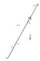
- FIG. 3is an embodiment of a thermocouple of the present invention
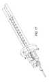
- FIG. 4is an exploded view of a portion of the thermocouple of FIG. 3 ;
- FIG. 5is a magnified view of a bead junction
- FIG. 6is a side view of an embodiment of a support member
- FIG. 7is a first end view of the support member of FIG. 6 ;
- FIG. 8is a second end view of the support member of FIG. 6 ;
- FIG. 9is a side view of an embodiment of a sheath
- FIG. 10is a side view of an embodiment of the assembled thermocouple of FIG. 3 ;
- FIG. 11is a cross-sectional view of the thermocouple of FIG. 10 ;
- FIG. 12Ais a top perspective view of a first retainer
- FIG. 12Bis a cross-sectional view of the first retainer of FIG. 12A ;
- FIG. 13Ais a top perspective view of an embodiment of a spacing member
- FIG. 13Bis a cross-sectional view of the spacing member of FIG. 13A ;
- FIG. 14Ais a top perspective view of a second retainer
- FIG. 14Bis a cross-sectional view of the second retainer of FIG. 14A ;
- FIG. 15is a cross-sectional view of a portion of the assembled thermocouple of FIG. 3 ;
- FIG. 16is an embodiment of a wire pattern for a first wire about a spacing member.
- FIG. 17is an embodiment of a wire pattern for a second wire about a spacing member.
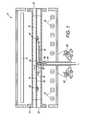
- the CVD reactor 10includes a reaction chamber 12 defining a reaction space 14 , heating elements 16 located on opposing sides of the reaction chamber 12 , and a substrate support mechanism 18 .
- the reaction chamber 12is an elongated member having an inlet 20 for allowing reactant gases to flow into the reaction space 14 and an outlet 22 through which the reactant gases and process by-products exit the reaction space 14 .
- the reaction chamber 12is formed of transparent quartz. It should be understood by one skilled in the art that the reaction chamber 12 may be formed of any other material sufficient to be substantially non-reactive relative to a deposition process therewithin.
- the heating elements 16form an upper bank and a lower bank, as shown in FIG. 1 .
- the heating elements 16are oriented in a spaced-apart manner relative to adjacent heating elements 16 within the same bank.
- the heating elements 16 of the upper bankare oriented substantially perpendicular relative to the heating elements 16 of the lower bank.
- the heating elements 16provide radiant energy to the reaction chamber 12 without appreciable absorption by the reaction chamber 12 walls.
- the heating elements 16are configured to provide radiant heat to the substrate 24 being processed as well as portions of the substrate support mechanism 18 , in an embodiment, a plurality of spot lamps 26 provide concentrated heat to the underside of the substrate support mechanism 18 to counteract a heat sink effect caused by cold support structures extending upwardly through the bottom wall of the reaction chamber 12 .
- the substrate support mechanism 18includes a substrate holder 28 , which receives the substrate 24 , and a support spider 30 , as shown in FIG. 1 .
- the support spider 30is connected to a shaft 32 that extends downwardly through a tube 34 depending from the lower wall of the reaction chamber 12 .
- a motor(not shown) is configured to rotate the shaft 32 , thereby rotating the substrate holder 28 and substrate 24 in a like manner during the deposition process.
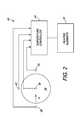
- a plurality of temperature sensorsare located adjacent to the substrate 24 and the substrate holder 28 for measuring temperatures at locations adjacent the substrate 24 , as shown in FIGS. 1-2 .
- the temperature sensorsinclude: a central temperature sensor 36 located adjacent to the lower surface of the substrate holder 28 , a leading edge temperature sensor 38 , a trailing edge temperature sensor 40 , and at least one side edge temperature sensor 42 .
- the leading and trailing edge temperature sensors 38 , 40are located adjacent to the front and rear edges of the substrate 24 relative to the direction of flow A of the reactant gases within the reaction space 14 .
- the temperature sensorsare configured to measure the temperature in the localized area immediately surrounding the tip of the temperature sensor.
- a temperature control system 45 for a CVD reactor 10as shown in FIG.
- the temperature control system 45includes any number of temperature sensors disposed at different locations for providing data to the controller 44 .
- thermocouple 46is a thermocouple 46 , as illustrated in FIGS. 3-15 .
- the other temperature sensors 36 , 38 , 40 , 42may be formed as optical pyrometers, thermocouples previously known in the art, and any combination thereof.
- the thermocouple 46as shown in FIGS. 3-5 , includes a sheath 48 , a support member 50 , a first retainer 52 , a first wire 54 , a second wire 56 , a spring 58 , a spacing member 60 , a second retainer 62 , and a plug 64 .
- the support member 50is a generally elongated, cylindrical member having a longitudinal axis B, as illustrated in FIGS. 5-8 .
- the support member 50includes a first distal end 66 and an opposing second distal end 68 .
- the support member 50has a generally circular cross-section extending along nearly the entire length of the support member 50 from the first distal end 66 .
- the support member 50is tapered to a substantially rectangular cross-section ( FIG. 8 ) near the second distal end 68 .
- the support member 50includes a pair of cut-outs 70 formed on opposing sides of the support member 50 in which each cut-out 70 includes a curved portion 72 extending from the outer surface of the support member 50 toward the longitudinal axis B thereof, as shown in FIG. 6 .
- Each cut-out 70further includes a substantially planar surface 74 extending from the curved portion 72 to the second distal end 68 .
- the cut-outs 70are formed as substantially linear tapers, wherein the entire tapered surfaces are substantially planar.
- the cut-outs 70allow the first and second wires 54 , 56 to remain in a spaced-apart relationship in which the first and second wires 54 , 56 are separated by the substantially rectangular-shaped cross-sectional portion of the support member 50 , as shown in FIG. 11 . It should be understood by one skilled in the art that the cut-outs 70 can be formed of any shape, provided the first and second wires 54 , 56 remain separated by at least a portion of the support member 50 .
- the support member 50has a substantially circular cross-sectional shape between the first and second distal ends 66 , 68 , wherein the support member 50 does not include cut-outs.
- the cross-sectional shape of the support member 50is square.
- the cross-sectional shape of the support member 50is oval. It should be understood by one skilled in the art that the cross-sectional shape of the support member 50 may be formed as any shape.
- the support member 50is formed of ceramic. It should be understood by one skilled in the art that the support member 50 may be formed of any type of material sufficient to withstand the cyclic temperature variations as well as the range of temperatures to which the thermocouple 46 is exposed. It should also be understood by one skilled in the art that although the illustrated thermocouple 46 is substantially linear, the thermocouple 46 may be formed of any shape sufficient to allow the measuring tip 76 of the thermocouple 46 to be disposed at a desired location for a localized temperature measurement.
- the support member 50further includes a first bore 78 and a second bore 80 , as shown in FIGS. 7-8 .
- the first and second bores 78 , 80are formed in the first distal end 66 and extend substantially parallel to the longitudinal axis 13 through the support member 50 .
- the first and second bores 78 , 80extend the entire length of the support member 50 between the first distal end 66 and the second distal end 68 .
- the first bore 78is configured to receive the first wire 54
- the second bore 80is configured to receive the second wire 56 . It should be understood by one skilled in the art that additional bores may be formed along the length of the support member 50 for receiving additional wires, allow air circulation therein, or any combination thereof.
- first and second bores 78 , 80extend from the first distal end 66 in a substantially parallel manner relative to the longitudinal axis B of the support member 50 , but the exit openings of the first and second bores 78 , 80 are spaced from the second distal end 68 .
- the exit openings of the first and second bores 78 , 80are formed on the curved portions 72 of the cut-outs 70 .
- the support member 50is at least partially disposed within a protective sheath 48 , as shown in FIGS. 4 and 9 - 11 .
- the sheath 48is formed of a transparent quartz material. It should be understood by one skilled in the art that the sheath 48 may be formed of any material sufficient to transmit heat from the environment immediately surrounding the measuring tip 76 through the sheath 48 for providing a temperature reading while being substantially non-reactant relative to the gases introduced into the reaction space 14 of the reaction chamber 12 ( FIG. 1 ).
- the transparent quartz materialallows a substantial amount of radiant energy from the substrate support mechanism 18 to pass therethrough without a detrimental increase in temperature of the sheath 48 .
- thermocouple 46 formed between the first and second wires 54 , 56is able to provide an accurate temperature measurement.
- the sheath 48has the same general cross-sectional shape as the support member 50 disposed therewithin, but the sheath 48 is slightly larger to provide a small gap between the inner surface of the sheath 48 and the outer surface of the support member 50 .
- the measuring tip 76forms one distal end of the sheath 48 , and an opening 84 is formed at the opposing distal end opposite the measuring tip 76 .
- the sheath 48may be coated with silicon nitride (SiN) or have other surface treatments applied thereto to extend the life of the sheath.
- a cap(not shown), such as a silicon-carbide (SiC) cap, is applied at the measuring tip 76 of the sheath to provide better heat transfer between the ambient environment and the junction 82 formed between the first and second wires 54 , 56 .
- first and second wires 54 , 56extend beyond the first distal end 66 of the support member 50 , as shown in FIG. 5 .
- the ends of the first and second wires 54 , 56 extending beyond the first distal end 66are fused together to form an electrical connection therebetween.
- the ends of the wires 54 , 56are melted together. It should be understood by one skilled in the art that any method of fusing the ends of the first and second wires 54 , 56 to provide an electrical connection therebetween can be used.
- the bonded wiresform a junction 82 located immediately adjacent to the first distal end 66 of the support member 50 .
- the free ends of the first and second wires 54 , 56 opposite the junction 82extend from the second distal end 68 of the support member 50 .
- the first and second wires 54 , 56are formed of dissimilar metals to form a thermocouple therebetween.
- the first wire 54is formed of platinum
- the second wire 56is formed of a Platinum alloy having 13% Rhodium. It should be understood by one skilled in the art that the first and second wires 54 , 56 can be formed of any dissimilar metals sufficient to form a thermocouple therebetween.
- the junction 82 of the first and second wires 54 , 56is disposed immediately adjacent to inner surface of the sheath 48 at the measuring tip 76 .
- the junction 82is in contact with the inner surface of the sheath 48 at the measuring tip 76 . In another embodiment, the junction 82 is spaced-apart from the inner surface of the sheath at the measuring tip 76 . It should be understood by one skilled in the art that the greater the distance that the junction 82 is spaced from the measuring tip 76 and the particular location to be measured, the less accurate the temperature measurement becomes.
- the diameter of the first and second wires 54 , 56are about 0.010 inches. In another embodiment, the diameter of the first and second wires is about 0.014 inches. It should be understood by one skilled in the art that the first and second wires 54 , 56 can be formed of any diameter, it should also be understood by one skilled in the art that the diameter of the first and second wires 54 , 56 may have a different diameter.
- the first and second bores 78 , 80are shaped to receive the first and second wires 54 , 56 , respectively.
- the first and second bores 78 , 80are configured to allow the first and second wires 54 , 56 to expand radially and axially therewithin. Accordingly, first and second bores 78 , 80 have a cross-section that is larger than the cross-section of the first and second wires 54 , 56 received therein.
- the first and second wires 54 , 56extend from the junction 82 , through the spaced-apart bores 78 , 80 formed in the support member 50 , and exit the first and second bores 78 , 80 adjacent to the second distal end 68 of the support member 50 , as shown in FIG. 11 .
- the second distal end 68 of the support member 50extends outwardly beyond the opening 84 of the sheath 48 .
- a collar 86is operatively connected to the outer surface of the support member 50 at a spaced-apart distance from the second distal end 68 of the support member 50 .
- the collar 86are formed separately from the support member 50 and later fixedly attached to the support member 50 .
- the support member 50 and the collar 86are formed as a single member. In an embodiment, at least a portion of the collar 86 contacts the inner surface of the sheath 48 to ensure that the support member 50 is secured within the sheath 48 to prevent substantial movement of the support member 50 therewithin.
- a first retainer 52is configured to surround a portion of the sheath 48 .
- the first retainer 52is a substantially hollow cylindrical member having a first end 88 and a second end 90 .
- the first retainer 52is formed of Delrin®.
- the first retainer 52is formed of a ceramic material.
- the first retainer 52is formed of an injection molded plastic.
- the first retainer 52includes a first aperture 92 formed through the first end 88 .
- the first retainer 52also includes a recessed area 94 configured to receive the sheath 48 , spacing member 60 , and second retainer 62 , as shown in FIG. 11 .
- the first retainer 52further includes a pair of notches 96 formed in the first end 88 . The notches 96 allow the thermocouple 46 to be positively located within a CVD reactor 10 .
- the spacing member 60is configured to receive the second distal end 68 of the support member 50 and the first and second wires 54 , 56 .
- the spacing member 60is disposed between the first retainer 52 and the second retainer 62 , in an embodiment, the spacing member 60 is formed of Delrin®. It should be understood by one skilled in the art that the spacing member 60 can be formed of any material including, but not limited to, plastic, metal, or quartz.
- the spacing member 60includes a base 100 , a first protruding portion 102 , and a second protruding portion 104 , as shown in FIGS. 13A-13B .
- the base 100includes a first surface 106 and an opposing second surface 108 .
- the first protruding portion 102extends from the first surface 106 of the base 100
- the second protruding portion 104extends from the second surface 108 of the base 100 .
- the first and second surfaces 106 , 108are substantially flat and oriented in a substantially parallel manner relative to each other.
- the first surface 106is configured to be located immediately adjacent to the surface of the recessed area 94 ( FIG. 12B ) surrounding the first aperture 92 of the first retainer 52 .
- the first protruding portion 102 of the spacing member 60includes a first aperture 110 formed therethrough, as shown in FIG. 13B .
- the first protruding portion 102is configured to be inserted into the opening 84 of the sheath 48 such that the first aperture 110 receives the portion of the support member 50 adjacent to the second distal end 68 thereof, as illustrated in FIG. 11 .
- the first aperture 110is sized and shaped to provide a friction, or interference, fit with the outer surface of the support member 50 such that the spacing member 60 is secured to the support member 50 .
- the first aperture 110is sized and shaped to allow the support member 50 received therein to freely translate within the first aperture 110 , thereby preventing additional compression or tension stresses during thermal expansion or contraction of the support member 50 .
- the outer surface of the first protruding portion 102is sized to be received in the opening 84 of the sheath 48 , as shown in FIG. 15 .
- the first protruding portion 102is sized and shaped to allow the spacing member 60 to freely translate within the opening 84 of the sheath 48 .
- the first protruding portion 102is sized and shaped to provide an interference, or friction fit between the spacing member 60 and the sheath 48 , thereby securing the spacing member 60 to the sheath 48 .
- the first protruding portion 102is shaped as a hollow, substantially cylindrical member.
- the cross-sectional shape of the first protruding portion 102should correspond to the cross-sectional shape of the inner surface of the sheath 48 adjacent to the opening 84 .
- the first aperture 110extends through the length of the first protruding portion 102 , through the base 100 , and through a portion of the second protruding portion 104 in a substantially linear manner, as shown in FIGS. 13A-13B .
- the cross-sectional shape of the first aperture 110is configured to be substantially the same cross-sectional shape as the portion of the support member 50 received therein.
- the second protruding portion 104extends from the second surface 108 of the base 100 , as shown in FIGS. 13A-13B .
- the second protruding portion 104is an elongated member having a flattened, elongated cross-sectional shape.
- the second protruding portion 104includes a body 114 , a second aperture 116 , a third aperture 118 , a first securing recess 120 , a second securing recess 122 , a first guide 124 , and a second guide 126 .
- the body 114includes a first side surface 128 , an opposing second side surface 130 , and a first and second opposing end surfaces 132 , 134 that extend between the first and second side surfaces 128 , 130 .
- the first and second side surfaces 128 , 130are formed as substantially parallel, planar surfaces. It should be understood by one skilled in the art that the first and second side surfaces 128 , 130 can be planar, ridged, concave, convex, or any other shape.
- the first and second end surfaces 132 , 134are formed as curved, or rounded, surfaces extending between the first and second side surfaces 128 , 130 . It should be understood by one skilled in the art that the first and second end surfaces 132 , 134 can be formed as planar surfaces, convex surfaces, concave surfaces, or have any other shape.
- a portion of the first aperture 110is formed through the length of the second protruding portion 104 , and a second aperture 116 is formed between the first and second side surfaces 128 , 130 of the body 114 of the second protruding portion 104 in a transverse manner relative to the first aperture 110 , as shown in FIGS. 13A-13B and 15 .
- the first aperture 110 and the second aperture 116intersect in a substantially perpendicular manner, thereby providing a window, or gap through the thickness of the body 114 of the second protruding portion 104 .
- the second aperture 116is an elongated slot formed through the thickness of the second protruding portion 104 . It should be understood by one skilled in the art that the second aperture 116 can be formed as any shape through the thickness of the second protruding portion 104 .
- the second protruding portion 104further includes a third aperture 118 formed therethrough in a substantially parallel manner relative to the first aperture 110 , as illustrated in FIGS. 13A-13B and 15 .
- the first and third apertures 110 , 118are substantially aligned along the longitudinal axis of the spacing member 60 .
- the cross-section of the third aperture 118is elongated and corresponds to the cross-section of the second distal end 68 of the support member 50 such that the third aperture 118 of the spacing member 60 receives the second distal end 68 of the support member 50 and the elongated shape prevents rotation of the support member 50 relative to the spacing member 60 .
- the cross-section of the third aperture 118is circular to receive the second distal end 68 of the support member 50 such that the orientation of the spacing member 60 relative to the support member 50 can be adjustable. It should be understood by one skilled in the art that the cross-section of the third aperture 118 of the spacing member 60 should be configured to receive the second distal end 68 of the support member 50 .
- the third aperture 118is sized and shaped to receive the second distal end 68 of the support member 50 in an interference, or friction fit, thereby securing the spacing member 60 to the support member 50 .
- the third aperture 118is sized and shaped to receive the second distal end 68 of the support member 50 such that the support member 50 can freely translate within the third aperture 118 during thermal expansion of the support member 50 .
- the first and second securing recesses 120 , 122form recessed regions extending radially inward from the first and second end surfaces 132 , 134 , respectively, of the second protruding portion 104 , as shown in FIG. 13A .
- the first and second securing recesses 120 , 122are configured to receive the first and second wires 54 , 56 when assembled, as illustrated in FIGS. 15-17 .
- the first guide 124is a recessed region formed into the thickness of the body 114 of the second protruding portion 104 from the second securing recess 122 .
- the first guide 124is configured to receive the first wire 54 , as shown in FIG. 16 .
- the first guide 124is oriented in a substantially parallel manner relative to the second aperture 116 .
- the second guide 126is a recessed region formed into the thickness of the body 114 from the end 136 of the second protruding portion 104 .
- the second guide 126is oriented in a substantially parallel manner relative to the second aperture 116 .
- the second guide 126intersects, or passes through, the third aperture 118 in a substantially perpendicular manner.
- the second guide 126is configured to receive the first and second wires 54 , 56 , as illustrated in FIGS. 16-17 .
- a locating member 109extends from the second surface 108 of the spacing member 60 and is received by a corresponding notch or recess 112 ( FIG. 14A ) formed in the second retainer 62 , thereby allowing the spacing member 60 to be positively located relative to the second retainer 62 .
- the locating member 109is received in the notch 112 to prevent rotation of the spacing member 60 relative to the second retainer 62 .
- the locating member 109extends from the first surface 106 and is received by a corresponding notch or recess (not shown) formed in the first retainer 52 , thereby allowing the spacing member 60 to be positively located relative to the first retainer 52 .
- the spacing member 60is secured between the first retainer 52 and the second retainer 62 , as illustrated in FIG. 11 .
- the second retainer 62as shown in FIGS. 14A-14B is a substantially cylindrical member having a flange 138 and a body 140 extending from the flange 138 .
- the second retainer 62includes a first end surface 142 and a second end surface 144 .
- the second retainer 62is formed as a substantially cylindrical member, wherein the second securing member has an aperture 146 extending along the longitudinal axis thereof.
- the second retainer 62also includes a notch 112 formed through the radial thickness of the flange 138 and the body 140 .
- the notch 112is configured to receive the locating member 109 extending from the second surface 108 of the base 100 of the spacing member 60 .
- the spacing member 60 and the second retainer 62are operatively connected such that the spacing member 60 does not rotate relative to the second retainer 62 .
- the aperture 146 of the second retainer 62is configured to receive the second protruding portion 104 of the spacing member 60 , as shown in FIG. 11 , such that a portion of the second protruding portion 104 of the spacing member 60 extends longitudinally beyond the second end surface 144 of the second retainer 62 .
- first end surface 142 of the second retainer 62is configured to be in an abutting relationship with the second surface of the base 100 of the spacing member 60 and the flange 138 of the second retainer 62 is configured to be in an abutting relationship with the second end 90 of the first retainer 52 .
- Assembly of the thermocouple 46includes inserting the first wire 54 through the first bore 78 adjacent the second distal end 68 of the support member 50 and inserting the second wire 56 through the second bore 80 adjacent the second distal end 68 of the support member 50 .
- first and second wires 54 , 56can be inserted into the first and second bores 78 , 80 , respectively, at the first distal end 66 of the support member 50 .
- the first and second wires 54 , 56are threaded through the first and second bores 78 , 80 such that a portion of the first and second wires 54 , 56 extend beyond the first distal end 66 of the support member 50 .
- junction 82The exposed ends of the first and second wires 54 , 56 adjacent the first distal end 66 of the support member 50 are then fused together to form a junction 82 .
- the support member 50 with the first and second wires 54 , 56 disposed thereinis inserted into the sheath 48 such that the junction 82 is in contact with the inner surface of the sheath 48 at the measuring tip 76 . It should be understood by one skilled in the art that the junction 82 can also be spaced apart from the inner surface of the sheath 48 .
- the spacing member 60is secured to the sheath 48 .
- the first protruding portion 102 of the spacing member 60is inserted into the opening 84 of the sheath 48 such that the second distal end 58 of the support member 50 is received in the first and third apertures 110 , 118 of the spacing member 60 .
- the first surface 106 of the base 100 of the spacing member 60contacts the surface surrounding the opening 84 of the sheath 48 .
- the spacing member 60is operatively connected to the sheath 48 such that the spacing member remains secured to the sheath 48 during the cyclical temperature changes due to processing in the CVD chamber 10 . Because the spacing member 60 is secured to the sheath 48 , the support member 50 is free to translate radially and along the longitudinal axis within the first and third apertures 110 , 118 . Allowing the support member 50 to move freely within the first and third apertures 110 , 118 prevents tension and compression forces to be introduced into the support member 50 during thermal expansion or contraction thereof.
- the first and second wires 54 , 56exit the first and second bores 78 , 80 , respectively, within the second aperture 116 of the spacing member 60 . While the first and second wires 54 , 56 remain separated by the support member 50 within the second aperture 116 , the first and second wires 54 , 56 are wound in a pattern about the spacing member 60 .
- a Teflon® tube 150is slid over both the first and second wires 54 , 56 to prevent the wires from contacting each other and causing a short circuit therebetween.
- the first wire 54exits the second aperture 116 near the end adjacent to the second distal end 68 of the support member 50 .
- the first wire 54extends along the first side surface 128 of the spacing member 60 adjacent to the second aperture 116 , wherein the first wire 54 forms a generally U-shaped pattern along the first side surface 128 .
- the first wire 54then extends along the first side surface 128 adjacent to the end of the second aperture 116 toward the end 136 of the second protruding portion 104 .
- the first wire 54is then disposed within the second guide 125 , extending from the first side surface 128 to the second side surface 130 .
- the first wire 54then extends adjacent to the second side surface 130 from the second guide 126 to the first guide 124 .
- the first wire 54extends through the first guide 124 from the second side surface 130 to the first side surface 128 , then the first wire 54 extends along the first side surface 128 from the first guide 124 toward the end 136 of the second protruding portion 104 .
- the first wire 54extends away from the spacing member 60 from the end 136 .
- the second wire 56exits the second aperture 116 near the end adjacent to the second distal end 68 of the support member 50 .
- the second wire 56exits the second aperture 116 in a direction opposite the direction from which the first wire 54 exits the second aperture 116 .
- the second wire 56extends along the second side surface 130 of the spacing member 60 adjacent to the second aperture 116 , wherein the second wire 56 forms a generally U-shaped pattern along the second side surface 130 .
- the second wire 56then extends along the second side surface 130 adjacent to the end of the second aperture 116 toward the end 136 of the second protruding portion 104 .
- the second wire 56is then disposed within the second guide 126 , extending from the second side surface 130 to the first side surface 128 .
- the second wire 56then extends adjacent to the first side surface 128 from the second guide 126 to the first guide 124 .
- the second wire 56extends through the first guide 124 from the first side surface 128 to the second side surface 130 , then the second wire 56 extends along the second side surface 130 from the first guide 124 toward the end 136 of the second protruding portion 104 .
- the second wire 56extends away from the spacing member 60 from the end 136 along with the first wire 54 .
- first and second wires 54 , 56are disposed about the first securing recess 120 and second securing recess 122 to secure the first and second wires 54 , 56 to the spacing member 60 . It should be understood by one skilled in the art that a portion of the first and second wires 54 , 56 are bare, or uncovered, within the second aperture 116 of the spacing member 60 , but the Teflon® tubes 150 covering the wires as they exit the second aperture 116 protect the wires during transport, installation, and in operation.
- the sheath 48 , support member 50 , and spacing member 60are then inserted through the first aperture 92 of the first retainer 52 until the flange defining the opening 84 of the sheath 48 contacts the surface of the recessed area 94 surrounding the first aperture 92 of the first retainer 52 .
- the first aperture 92 of the first retainer 52is shaped to allow the first surface 106 of the base 100 of the spacing member 60 to contact the surface of the recessed area 94 surrounding the first aperture 92 of the first retainer 52 in an abutting manner.
- the first surface 106 of the spacing member 60is spaced apart from the surface of the recessed area 94 surrounding the first aperture 92 of the first retainer 52 .
- the second retainer 62is disposed over the second protruding portion 104 of the spacing member 60 such that the second protruding portion 104 is received within the aperture 146 formed in the second retainer 62 .
- the end 136 of the second protruding portion 104 of the spacing member 60extends beyond the second end surface 144 of the second retainer 62 .
- the notch 112 formed in the second retainer 62receives the locating member 109 of the spacing member 60 to positively locate the spacing member 60 relative to the second retainer 62 .
- the first end surface 142 of the second retainer 62When assembled, the first end surface 142 of the second retainer 62 is in an abutting relationship with the second surface 108 of the base 100 of the spacing member 60 , wherein the body 140 of the second retainer 62 is disposed within the recessed area 94 of the first retainer 52 .
- the second retainer 62is fixedly attached to the first retainer 52 by glue or any other means of securing the first and second retainers 52 , 62 to prevent rotation therebetween.
- the second retainer 62is removeably connected to the first retainer 52 .
- the first and second wires 54 , 56 covered by the Teflon® tubes 150extend from the second retainer 62 and are operatively connected to the plug 64 to complete the assembly of the thermocouple 46 .
- the thermocouple 46may be used as a central temperature sensor 36 or it may be used as a leading edge temperature sensor 38 , trailing edge temperature sensor 40 , or side edge temperature sensor 42 , as illustrated in FIG. 2 .
- the thermocouple 46is employed as a central temperature sensor 36 ( FIG. 1 )
- the measuring tip 76is disposed within a recessed formed in the lower surface of the substrate holder 28 .
- the measuring tip 76 of the thermocouple 46is configured to measure the temperature of the substrate holder 28 immediately adjacent thereto.
- the temperature within the reaction chamber 12often cycles between significantly high and low temperatures.
- the temperature within the reaction chambermay be between room temperature and about 1200° C. or more.
- the coefficient of thermal expansion of the support memberis different than the coefficient of thermal expansion of the first and second wires.
- the first and second wireswere secured together and to the second distal end of the support member through which the wires extended. Because the difference between the coefficients of thermal expansion and temperatures of the wires and the support member, the wires and support member would expand and contract at different rates as the temperatures within the CVD reactor 10 increased or decreased. Prolonged exposure to these cyclical temperatures in which the wires were not free to thermally expand or contract freely with respect to the support member caused grain slip in the wires, resulting in failure of the thermocouple.
- the present designallows the wires to freely expand in the longitudinal direction relative to the support member, thereby reducing the potential stress or strain in the wires during thermal expansion or contraction.
- the first and second wires 54 , 56are formed of different metals and accordingly have different coefficients of thermal expansion.
- the support member 50is formed of a different material such that the support member 50 has a different coefficient of thermal expansion relative to the first and second wires 54 , 56 . Because each of these members have a different coefficient of thermal expansion, each of them will expand and contract differently in response to the same temperature change.
- the spacing member 60allows the first and second wires 54 , 56 to independently thermally expand relative to each other.
- the spacing member 60also allows the support member 50 to independently thermally expand relative to the first and second wires 54 , 56 .
- the spacing member 60is removably attached to the sheath 48 such that the spacing member 60 remains fixedly attached to the sheath 48 during operation of the thermocouple 46 , but the spacing member 60 is removable from the sheath 48 to allow for refurbishment or disassembly of the thermocouple 46 .
- the support member 50is received in the substantially aligned first and third apertures 110 , 118 of the spacing member 60 such that the support member 50 is allowed to expand radially and in a longitudinal manner in response to thermal expansion. Because the support member 50 can freely expand due to the temperature changes to which the thermocouple 46 is exposed, there are no compression or tension stresses introduced into the support member 50 that would otherwise be introduced if the support member 50 were secured to the sheath 48 .
- first and second wires 54 , 56are likewise allowed to freely expand radially and along their longitudinal axes within the support member 50 and about the spacing member 60 .
- the second aperture 116 of the spacing member 60maintains the first and second wires 54 , 56 in a spaced-apart relationship to prevent a short circuit, but the second aperture 116 also allows the first and second wires 54 , 56 to thermally expand at a different rate than the support member 50 . Because the coefficient of thermal expansion of the first and second wires 54 , 56 is different than the support member 50 , the first and second wires 54 , 56 should be allowed sufficient space to expand and contract at a different rate than the support member 50 due to thermal changes to both.
- the second aperture 116 of the spacing member 60allows the first and second wires 54 , 56 to thermally expand and contract at a different rate relative to the support member 50 .
- the first and second wires 54 , 56exit the first and second bores 78 , 80 , respectively, of the support member 50 within the second aperture 116 .
- the first and second wires 54 , 56exit the second aperture 116 and form a U-shaped loop adjacent to the opposing side surface of the spacing member 60 .
- the pattern formed by the first and second wires 54 , 56 as they exit the bores 78 , 80allow the wires to expand longitudinally at a different rate than the support member 50 , thereby preventing grain slip along the wires and also preventing compression or tension stresses from being introduced into the first and second wires 54 , 56 .
Landscapes
- Chemical & Material Sciences (AREA)
- Physics & Mathematics (AREA)
- General Physics & Mathematics (AREA)
- General Chemical & Material Sciences (AREA)
- Chemical Kinetics & Catalysis (AREA)
- Engineering & Computer Science (AREA)
- Materials Engineering (AREA)
- Mechanical Engineering (AREA)
- Metallurgy (AREA)
- Organic Chemistry (AREA)
- Measuring Temperature Or Quantity Of Heat (AREA)
- Chemical Vapour Deposition (AREA)
Abstract
Description
Claims (18)
Priority Applications (1)
| Application Number | Priority Date | Filing Date | Title |
|---|---|---|---|
| US13/563,274US8616765B2 (en) | 2008-12-08 | 2012-07-31 | Thermocouple |
Applications Claiming Priority (2)
| Application Number | Priority Date | Filing Date | Title |
|---|---|---|---|
| US12/330,096US8262287B2 (en) | 2008-12-08 | 2008-12-08 | Thermocouple |
| US13/563,274US8616765B2 (en) | 2008-12-08 | 2012-07-31 | Thermocouple |
Related Parent Applications (1)
| Application Number | Title | Priority Date | Filing Date |
|---|---|---|---|
| US12/330,096ContinuationUS8262287B2 (en) | 2008-12-08 | 2008-12-08 | Thermocouple |
Publications (2)
| Publication Number | Publication Date |
|---|---|
| US20120310440A1 US20120310440A1 (en) | 2012-12-06 |
| US8616765B2true US8616765B2 (en) | 2013-12-31 |
Family
ID=42231995
Family Applications (2)
| Application Number | Title | Priority Date | Filing Date |
|---|---|---|---|
| US12/330,096Active2030-07-06US8262287B2 (en) | 2008-12-08 | 2008-12-08 | Thermocouple |
| US13/563,274ActiveUS8616765B2 (en) | 2008-12-08 | 2012-07-31 | Thermocouple |
Family Applications Before (1)
| Application Number | Title | Priority Date | Filing Date |
|---|---|---|---|
| US12/330,096Active2030-07-06US8262287B2 (en) | 2008-12-08 | 2008-12-08 | Thermocouple |
Country Status (3)
| Country | Link |
|---|---|
| US (2) | US8262287B2 (en) |
| EP (1) | EP2370996B1 (en) |
| WO (1) | WO2010077533A2 (en) |
Cited By (355)
| Publication number | Priority date | Publication date | Assignee | Title |
|---|---|---|---|---|
| US9267850B2 (en) | 2009-05-06 | 2016-02-23 | Asm America, Inc. | Thermocouple assembly with guarded thermocouple junction |
| US9297705B2 (en) | 2009-05-06 | 2016-03-29 | Asm America, Inc. | Smart temperature measuring device |
| US20180335351A1 (en)* | 2017-05-18 | 2018-11-22 | Sensata Technlogies, Inc. | Floating conductor housing |
| US10229833B2 (en) | 2016-11-01 | 2019-03-12 | Asm Ip Holding B.V. | Methods for forming a transition metal nitride film on a substrate by atomic layer deposition and related semiconductor device structures |
| US10249577B2 (en) | 2016-05-17 | 2019-04-02 | Asm Ip Holding B.V. | Method of forming metal interconnection and method of fabricating semiconductor apparatus using the method |
| US10249524B2 (en) | 2017-08-09 | 2019-04-02 | Asm Ip Holding B.V. | Cassette holder assembly for a substrate cassette and holding member for use in such assembly |
| US10262859B2 (en) | 2016-03-24 | 2019-04-16 | Asm Ip Holding B.V. | Process for forming a film on a substrate using multi-port injection assemblies |
| US10269558B2 (en) | 2016-12-22 | 2019-04-23 | Asm Ip Holding B.V. | Method of forming a structure on a substrate |
| US10276355B2 (en) | 2015-03-12 | 2019-04-30 | Asm Ip Holding B.V. | Multi-zone reactor, system including the reactor, and method of using the same |
| US10283353B2 (en) | 2017-03-29 | 2019-05-07 | Asm Ip Holding B.V. | Method of reforming insulating film deposited on substrate with recess pattern |
| US10290508B1 (en) | 2017-12-05 | 2019-05-14 | Asm Ip Holding B.V. | Method for forming vertical spacers for spacer-defined patterning |
| US10312055B2 (en) | 2017-07-26 | 2019-06-04 | Asm Ip Holding B.V. | Method of depositing film by PEALD using negative bias |
| US10312129B2 (en) | 2015-09-29 | 2019-06-04 | Asm Ip Holding B.V. | Variable adjustment for precise matching of multiple chamber cavity housings |
| US10319588B2 (en) | 2017-10-10 | 2019-06-11 | Asm Ip Holding B.V. | Method for depositing a metal chalcogenide on a substrate by cyclical deposition |
| US10322384B2 (en) | 2015-11-09 | 2019-06-18 | Asm Ip Holding B.V. | Counter flow mixer for process chamber |
| US10340125B2 (en) | 2013-03-08 | 2019-07-02 | Asm Ip Holding B.V. | Pulsed remote plasma method and system |
| US10340135B2 (en) | 2016-11-28 | 2019-07-02 | Asm Ip Holding B.V. | Method of topologically restricted plasma-enhanced cyclic deposition of silicon or metal nitride |
| US10343920B2 (en) | 2016-03-18 | 2019-07-09 | Asm Ip Holding B.V. | Aligned carbon nanotubes |
| US10361201B2 (en) | 2013-09-27 | 2019-07-23 | Asm Ip Holding B.V. | Semiconductor structure and device formed using selective epitaxial process |
| US10364493B2 (en) | 2016-08-25 | 2019-07-30 | Asm Ip Holding B.V. | Exhaust apparatus and substrate processing apparatus having an exhaust line with a first ring having at least one hole on a lateral side thereof placed in the exhaust line |
| US10364496B2 (en) | 2011-06-27 | 2019-07-30 | Asm Ip Holding B.V. | Dual section module having shared and unshared mass flow controllers |
| US10367080B2 (en) | 2016-05-02 | 2019-07-30 | Asm Ip Holding B.V. | Method of forming a germanium oxynitride film |
| US10366864B2 (en) | 2013-03-08 | 2019-07-30 | Asm Ip Holding B.V. | Method and system for in-situ formation of intermediate reactive species |
| US10373794B2 (en) | 2015-10-29 | 2019-08-06 | Lam Research Corporation | Systems and methods for filtering radio frequencies from a signal of a thermocouple and controlling a temperature of an electrode in a plasma chamber |
| US10381226B2 (en) | 2016-07-27 | 2019-08-13 | Asm Ip Holding B.V. | Method of processing substrate |
| US10378106B2 (en) | 2008-11-14 | 2019-08-13 | Asm Ip Holding B.V. | Method of forming insulation film by modified PEALD |
| US10381219B1 (en) | 2018-10-25 | 2019-08-13 | Asm Ip Holding B.V. | Methods for forming a silicon nitride film |
| US10388513B1 (en) | 2018-07-03 | 2019-08-20 | Asm Ip Holding B.V. | Method for depositing silicon-free carbon-containing film as gap-fill layer by pulse plasma-assisted deposition |
| US10388509B2 (en) | 2016-06-28 | 2019-08-20 | Asm Ip Holding B.V. | Formation of epitaxial layers via dislocation filtering |
| US10395919B2 (en) | 2016-07-28 | 2019-08-27 | Asm Ip Holding B.V. | Method and apparatus for filling a gap |
| US10403504B2 (en) | 2017-10-05 | 2019-09-03 | Asm Ip Holding B.V. | Method for selectively depositing a metallic film on a substrate |
| US10410943B2 (en) | 2016-10-13 | 2019-09-10 | Asm Ip Holding B.V. | Method for passivating a surface of a semiconductor and related systems |
| US10438965B2 (en) | 2014-12-22 | 2019-10-08 | Asm Ip Holding B.V. | Semiconductor device and manufacturing method thereof |
| US10435790B2 (en) | 2016-11-01 | 2019-10-08 | Asm Ip Holding B.V. | Method of subatmospheric plasma-enhanced ALD using capacitively coupled electrodes with narrow gap |
| US10446393B2 (en) | 2017-05-08 | 2019-10-15 | Asm Ip Holding B.V. | Methods for forming silicon-containing epitaxial layers and related semiconductor device structures |
| US10458018B2 (en) | 2015-06-26 | 2019-10-29 | Asm Ip Holding B.V. | Structures including metal carbide material, devices including the structures, and methods of forming same |
| US10468262B2 (en) | 2017-02-15 | 2019-11-05 | Asm Ip Holding B.V. | Methods for forming a metallic film on a substrate by a cyclical deposition and related semiconductor device structures |
| US10468251B2 (en) | 2016-02-19 | 2019-11-05 | Asm Ip Holding B.V. | Method for forming spacers using silicon nitride film for spacer-defined multiple patterning |
| US10480072B2 (en) | 2009-04-06 | 2019-11-19 | Asm Ip Holding B.V. | Semiconductor processing reactor and components thereof |
| US10483099B1 (en) | 2018-07-26 | 2019-11-19 | Asm Ip Holding B.V. | Method for forming thermally stable organosilicon polymer film |
| US10504742B2 (en) | 2017-05-31 | 2019-12-10 | Asm Ip Holding B.V. | Method of atomic layer etching using hydrogen plasma |
| US10501866B2 (en) | 2016-03-09 | 2019-12-10 | Asm Ip Holding B.V. | Gas distribution apparatus for improved film uniformity in an epitaxial system |
| US10510536B2 (en) | 2018-03-29 | 2019-12-17 | Asm Ip Holding B.V. | Method of depositing a co-doped polysilicon film on a surface of a substrate within a reaction chamber |
| US10529563B2 (en) | 2017-03-29 | 2020-01-07 | Asm Ip Holdings B.V. | Method for forming doped metal oxide films on a substrate by cyclical deposition and related semiconductor device structures |
| US10529542B2 (en) | 2015-03-11 | 2020-01-07 | Asm Ip Holdings B.V. | Cross-flow reactor and method |
| US10529554B2 (en) | 2016-02-19 | 2020-01-07 | Asm Ip Holding B.V. | Method for forming silicon nitride film selectively on sidewalls or flat surfaces of trenches |
| US10535516B2 (en) | 2018-02-01 | 2020-01-14 | Asm Ip Holdings B.V. | Method for depositing a semiconductor structure on a surface of a substrate and related semiconductor structures |
| US10541333B2 (en) | 2017-07-19 | 2020-01-21 | Asm Ip Holding B.V. | Method for depositing a group IV semiconductor and related semiconductor device structures |
| US10541173B2 (en) | 2016-07-08 | 2020-01-21 | Asm Ip Holding B.V. | Selective deposition method to form air gaps |
| US10559458B1 (en) | 2018-11-26 | 2020-02-11 | Asm Ip Holding B.V. | Method of forming oxynitride film |
| US10566223B2 (en) | 2012-08-28 | 2020-02-18 | Asm Ip Holdings B.V. | Systems and methods for dynamic semiconductor process scheduling |
| US10561975B2 (en) | 2014-10-07 | 2020-02-18 | Asm Ip Holdings B.V. | Variable conductance gas distribution apparatus and method |
| US10590535B2 (en) | 2017-07-26 | 2020-03-17 | Asm Ip Holdings B.V. | Chemical treatment, deposition and/or infiltration apparatus and method for using the same |
| US10600673B2 (en) | 2015-07-07 | 2020-03-24 | Asm Ip Holding B.V. | Magnetic susceptor to baseplate seal |
| US10604847B2 (en) | 2014-03-18 | 2020-03-31 | Asm Ip Holding B.V. | Gas distribution system, reactor including the system, and methods of using the same |
| US10605530B2 (en) | 2017-07-26 | 2020-03-31 | Asm Ip Holding B.V. | Assembly of a liner and a flange for a vertical furnace as well as the liner and the vertical furnace |
| US10607895B2 (en) | 2017-09-18 | 2020-03-31 | Asm Ip Holdings B.V. | Method for forming a semiconductor device structure comprising a gate fill metal |
| US10612136B2 (en) | 2018-06-29 | 2020-04-07 | ASM IP Holding, B.V. | Temperature-controlled flange and reactor system including same |
| USD880437S1 (en) | 2018-02-01 | 2020-04-07 | Asm Ip Holding B.V. | Gas supply plate for semiconductor manufacturing apparatus |
| US10612137B2 (en) | 2016-07-08 | 2020-04-07 | Asm Ip Holdings B.V. | Organic reactants for atomic layer deposition |
| US10622375B2 (en) | 2016-11-07 | 2020-04-14 | Asm Ip Holding B.V. | Method of processing a substrate and a device manufactured by using the method |
| US10643826B2 (en) | 2016-10-26 | 2020-05-05 | Asm Ip Holdings B.V. | Methods for thermally calibrating reaction chambers |
| US10643904B2 (en) | 2016-11-01 | 2020-05-05 | Asm Ip Holdings B.V. | Methods for forming a semiconductor device and related semiconductor device structures |
| US10658181B2 (en) | 2018-02-20 | 2020-05-19 | Asm Ip Holding B.V. | Method of spacer-defined direct patterning in semiconductor fabrication |
| US10658205B2 (en) | 2017-09-28 | 2020-05-19 | Asm Ip Holdings B.V. | Chemical dispensing apparatus and methods for dispensing a chemical to a reaction chamber |
| US10655221B2 (en) | 2017-02-09 | 2020-05-19 | Asm Ip Holding B.V. | Method for depositing oxide film by thermal ALD and PEALD |
| US10665452B2 (en) | 2016-05-02 | 2020-05-26 | Asm Ip Holdings B.V. | Source/drain performance through conformal solid state doping |
| US10683571B2 (en) | 2014-02-25 | 2020-06-16 | Asm Ip Holding B.V. | Gas supply manifold and method of supplying gases to chamber using same |
| US10685834B2 (en) | 2017-07-05 | 2020-06-16 | Asm Ip Holdings B.V. | Methods for forming a silicon germanium tin layer and related semiconductor device structures |
| US10692741B2 (en) | 2017-08-08 | 2020-06-23 | Asm Ip Holdings B.V. | Radiation shield |
| US10707106B2 (en) | 2011-06-06 | 2020-07-07 | Asm Ip Holding B.V. | High-throughput semiconductor-processing apparatus equipped with multiple dual-chamber modules |
| US10714350B2 (en) | 2016-11-01 | 2020-07-14 | ASM IP Holdings, B.V. | Methods for forming a transition metal niobium nitride film on a substrate by atomic layer deposition and related semiconductor device structures |
| US10714335B2 (en) | 2017-04-25 | 2020-07-14 | Asm Ip Holding B.V. | Method of depositing thin film and method of manufacturing semiconductor device |
| US10714315B2 (en) | 2012-10-12 | 2020-07-14 | Asm Ip Holdings B.V. | Semiconductor reaction chamber showerhead |
| US10714385B2 (en) | 2016-07-19 | 2020-07-14 | Asm Ip Holding B.V. | Selective deposition of tungsten |
| US10731249B2 (en) | 2018-02-15 | 2020-08-04 | Asm Ip Holding B.V. | Method of forming a transition metal containing film on a substrate by a cyclical deposition process, a method for supplying a transition metal halide compound to a reaction chamber, and related vapor deposition apparatus |
| US10734497B2 (en) | 2017-07-18 | 2020-08-04 | Asm Ip Holding B.V. | Methods for forming a semiconductor device structure and related semiconductor device structures |
| US10734244B2 (en) | 2017-11-16 | 2020-08-04 | Asm Ip Holding B.V. | Method of processing a substrate and a device manufactured by the same |
| US10741385B2 (en) | 2016-07-28 | 2020-08-11 | Asm Ip Holding B.V. | Method and apparatus for filling a gap |
| US10755922B2 (en) | 2018-07-03 | 2020-08-25 | Asm Ip Holding B.V. | Method for depositing silicon-free carbon-containing film as gap-fill layer by pulse plasma-assisted deposition |
| US10767789B2 (en) | 2018-07-16 | 2020-09-08 | Asm Ip Holding B.V. | Diaphragm valves, valve components, and methods for forming valve components |
| US10770336B2 (en) | 2017-08-08 | 2020-09-08 | Asm Ip Holding B.V. | Substrate lift mechanism and reactor including same |
| US10770286B2 (en) | 2017-05-08 | 2020-09-08 | Asm Ip Holdings B.V. | Methods for selectively forming a silicon nitride film on a substrate and related semiconductor device structures |
| US10787741B2 (en) | 2014-08-21 | 2020-09-29 | Asm Ip Holding B.V. | Method and system for in situ formation of gas-phase compounds |
| US10797133B2 (en) | 2018-06-21 | 2020-10-06 | Asm Ip Holding B.V. | Method for depositing a phosphorus doped silicon arsenide film and related semiconductor device structures |
| US10804098B2 (en) | 2009-08-14 | 2020-10-13 | Asm Ip Holding B.V. | Systems and methods for thin-film deposition of metal oxides using excited nitrogen-oxygen species |
| US10811256B2 (en) | 2018-10-16 | 2020-10-20 | Asm Ip Holding B.V. | Method for etching a carbon-containing feature |
| USD900036S1 (en) | 2017-08-24 | 2020-10-27 | Asm Ip Holding B.V. | Heater electrical connector and adapter |
| US10818758B2 (en) | 2018-11-16 | 2020-10-27 | Asm Ip Holding B.V. | Methods for forming a metal silicate film on a substrate in a reaction chamber and related semiconductor device structures |
| US10829852B2 (en) | 2018-08-16 | 2020-11-10 | Asm Ip Holding B.V. | Gas distribution device for a wafer processing apparatus |
| US10832903B2 (en) | 2011-10-28 | 2020-11-10 | Asm Ip Holding B.V. | Process feed management for semiconductor substrate processing |
| US10847371B2 (en) | 2018-03-27 | 2020-11-24 | Asm Ip Holding B.V. | Method of forming an electrode on a substrate and a semiconductor device structure including an electrode |
| US10847365B2 (en) | 2018-10-11 | 2020-11-24 | Asm Ip Holding B.V. | Method of forming conformal silicon carbide film by cyclic CVD |
| US10847366B2 (en) | 2018-11-16 | 2020-11-24 | Asm Ip Holding B.V. | Methods for depositing a transition metal chalcogenide film on a substrate by a cyclical deposition process |
| US10844484B2 (en) | 2017-09-22 | 2020-11-24 | Asm Ip Holding B.V. | Apparatus for dispensing a vapor phase reactant to a reaction chamber and related methods |
| USD903477S1 (en) | 2018-01-24 | 2020-12-01 | Asm Ip Holdings B.V. | Metal clamp |
| US10854498B2 (en) | 2011-07-15 | 2020-12-01 | Asm Ip Holding B.V. | Wafer-supporting device and method for producing same |
| US10851456B2 (en) | 2016-04-21 | 2020-12-01 | Asm Ip Holding B.V. | Deposition of metal borides |
| US10858737B2 (en) | 2014-07-28 | 2020-12-08 | Asm Ip Holding B.V. | Showerhead assembly and components thereof |
| US10865475B2 (en) | 2016-04-21 | 2020-12-15 | Asm Ip Holding B.V. | Deposition of metal borides and silicides |
| US10867786B2 (en) | 2018-03-30 | 2020-12-15 | Asm Ip Holding B.V. | Substrate processing method |
| US10867788B2 (en) | 2016-12-28 | 2020-12-15 | Asm Ip Holding B.V. | Method of forming a structure on a substrate |
| US10872771B2 (en) | 2018-01-16 | 2020-12-22 | Asm Ip Holding B. V. | Method for depositing a material film on a substrate within a reaction chamber by a cyclical deposition process and related device structures |
| US10883175B2 (en) | 2018-08-09 | 2021-01-05 | Asm Ip Holding B.V. | Vertical furnace for processing substrates and a liner for use therein |
| US10886123B2 (en) | 2017-06-02 | 2021-01-05 | Asm Ip Holding B.V. | Methods for forming low temperature semiconductor layers and related semiconductor device structures |
| US10892156B2 (en) | 2017-05-08 | 2021-01-12 | Asm Ip Holding B.V. | Methods for forming a silicon nitride film on a substrate and related semiconductor device structures |
| US10896820B2 (en) | 2018-02-14 | 2021-01-19 | Asm Ip Holding B.V. | Method for depositing a ruthenium-containing film on a substrate by a cyclical deposition process |
| US10910262B2 (en) | 2017-11-16 | 2021-02-02 | Asm Ip Holding B.V. | Method of selectively depositing a capping layer structure on a semiconductor device structure |
| US10914004B2 (en) | 2018-06-29 | 2021-02-09 | Asm Ip Holding B.V. | Thin-film deposition method and manufacturing method of semiconductor device |
| US10923344B2 (en) | 2017-10-30 | 2021-02-16 | Asm Ip Holding B.V. | Methods for forming a semiconductor structure and related semiconductor structures |
| US10928731B2 (en) | 2017-09-21 | 2021-02-23 | Asm Ip Holding B.V. | Method of sequential infiltration synthesis treatment of infiltrateable material and structures and devices formed using same |
| US10934619B2 (en) | 2016-11-15 | 2021-03-02 | Asm Ip Holding B.V. | Gas supply unit and substrate processing apparatus including the gas supply unit |
| US10941490B2 (en) | 2014-10-07 | 2021-03-09 | Asm Ip Holding B.V. | Multiple temperature range susceptor, assembly, reactor and system including the susceptor, and methods of using the same |
| US10975470B2 (en) | 2018-02-23 | 2021-04-13 | Asm Ip Holding B.V. | Apparatus for detecting or monitoring for a chemical precursor in a high temperature environment |
| US11001925B2 (en) | 2016-12-19 | 2021-05-11 | Asm Ip Holding B.V. | Substrate processing apparatus |
| US11018002B2 (en) | 2017-07-19 | 2021-05-25 | Asm Ip Holding B.V. | Method for selectively depositing a Group IV semiconductor and related semiconductor device structures |
| US11015245B2 (en) | 2014-03-19 | 2021-05-25 | Asm Ip Holding B.V. | Gas-phase reactor and system having exhaust plenum and components thereof |
| US11018047B2 (en) | 2018-01-25 | 2021-05-25 | Asm Ip Holding B.V. | Hybrid lift pin |
| US11024523B2 (en) | 2018-09-11 | 2021-06-01 | Asm Ip Holding B.V. | Substrate processing apparatus and method |
| US11022879B2 (en) | 2017-11-24 | 2021-06-01 | Asm Ip Holding B.V. | Method of forming an enhanced unexposed photoresist layer |
| US11031242B2 (en) | 2018-11-07 | 2021-06-08 | Asm Ip Holding B.V. | Methods for depositing a boron doped silicon germanium film |
| USD922229S1 (en) | 2019-06-05 | 2021-06-15 | Asm Ip Holding B.V. | Device for controlling a temperature of a gas supply unit |
| US11049751B2 (en) | 2018-09-14 | 2021-06-29 | Asm Ip Holding B.V. | Cassette supply system to store and handle cassettes and processing apparatus equipped therewith |
| US11056567B2 (en) | 2018-05-11 | 2021-07-06 | Asm Ip Holding B.V. | Method of forming a doped metal carbide film on a substrate and related semiconductor device structures |
| US11053591B2 (en) | 2018-08-06 | 2021-07-06 | Asm Ip Holding B.V. | Multi-port gas injection system and reactor system including same |
| US11056344B2 (en) | 2017-08-30 | 2021-07-06 | Asm Ip Holding B.V. | Layer forming method |
| US11069510B2 (en) | 2017-08-30 | 2021-07-20 | Asm Ip Holding B.V. | Substrate processing apparatus |
| US11081345B2 (en) | 2018-02-06 | 2021-08-03 | Asm Ip Holding B.V. | Method of post-deposition treatment for silicon oxide film |
| US11088002B2 (en) | 2018-03-29 | 2021-08-10 | Asm Ip Holding B.V. | Substrate rack and a substrate processing system and method |
| US11087997B2 (en) | 2018-10-31 | 2021-08-10 | Asm Ip Holding B.V. | Substrate processing apparatus for processing substrates |
| US11114294B2 (en) | 2019-03-08 | 2021-09-07 | Asm Ip Holding B.V. | Structure including SiOC layer and method of forming same |
| US11114283B2 (en) | 2018-03-16 | 2021-09-07 | Asm Ip Holding B.V. | Reactor, system including the reactor, and methods of manufacturing and using same |
| USD930782S1 (en) | 2019-08-22 | 2021-09-14 | Asm Ip Holding B.V. | Gas distributor |
| US11127589B2 (en) | 2019-02-01 | 2021-09-21 | Asm Ip Holding B.V. | Method of topology-selective film formation of silicon oxide |
| US11127617B2 (en) | 2017-11-27 | 2021-09-21 | Asm Ip Holding B.V. | Storage device for storing wafer cassettes for use with a batch furnace |
| USD931978S1 (en) | 2019-06-27 | 2021-09-28 | Asm Ip Holding B.V. | Showerhead vacuum transport |
| US11139191B2 (en) | 2017-08-09 | 2021-10-05 | Asm Ip Holding B.V. | Storage apparatus for storing cassettes for substrates and processing apparatus equipped therewith |
| US11139308B2 (en) | 2015-12-29 | 2021-10-05 | Asm Ip Holding B.V. | Atomic layer deposition of III-V compounds to form V-NAND devices |
| US11158513B2 (en) | 2018-12-13 | 2021-10-26 | Asm Ip Holding B.V. | Methods for forming a rhenium-containing film on a substrate by a cyclical deposition process and related semiconductor device structures |
| US11171025B2 (en) | 2019-01-22 | 2021-11-09 | Asm Ip Holding B.V. | Substrate processing device |
| USD935572S1 (en) | 2019-05-24 | 2021-11-09 | Asm Ip Holding B.V. | Gas channel plate |
| US11205585B2 (en) | 2016-07-28 | 2021-12-21 | Asm Ip Holding B.V. | Substrate processing apparatus and method of operating the same |
| US11217444B2 (en) | 2018-11-30 | 2022-01-04 | Asm Ip Holding B.V. | Method for forming an ultraviolet radiation responsive metal oxide-containing film |
| USD940837S1 (en) | 2019-08-22 | 2022-01-11 | Asm Ip Holding B.V. | Electrode |
| US11222772B2 (en) | 2016-12-14 | 2022-01-11 | Asm Ip Holding B.V. | Substrate processing apparatus |
| US11227782B2 (en) | 2019-07-31 | 2022-01-18 | Asm Ip Holding B.V. | Vertical batch furnace assembly |
| US11227789B2 (en) | 2019-02-20 | 2022-01-18 | Asm Ip Holding B.V. | Method and apparatus for filling a recess formed within a substrate surface |
| US11230766B2 (en) | 2018-03-29 | 2022-01-25 | Asm Ip Holding B.V. | Substrate processing apparatus and method |
| US11232963B2 (en) | 2018-10-03 | 2022-01-25 | Asm Ip Holding B.V. | Substrate processing apparatus and method |
| US11233133B2 (en) | 2015-10-21 | 2022-01-25 | Asm Ip Holding B.V. | NbMC layers |
| US11251040B2 (en) | 2019-02-20 | 2022-02-15 | Asm Ip Holding B.V. | Cyclical deposition method including treatment step and apparatus for same |
| US11251068B2 (en) | 2018-10-19 | 2022-02-15 | Asm Ip Holding B.V. | Substrate processing apparatus and substrate processing method |
| USD944946S1 (en) | 2019-06-14 | 2022-03-01 | Asm Ip Holding B.V. | Shower plate |
| US11270899B2 (en) | 2018-06-04 | 2022-03-08 | Asm Ip Holding B.V. | Wafer handling chamber with moisture reduction |
| US11274369B2 (en) | 2018-09-11 | 2022-03-15 | Asm Ip Holding B.V. | Thin film deposition method |
| US11282698B2 (en) | 2019-07-19 | 2022-03-22 | Asm Ip Holding B.V. | Method of forming topology-controlled amorphous carbon polymer film |
| US11286562B2 (en) | 2018-06-08 | 2022-03-29 | Asm Ip Holding B.V. | Gas-phase chemical reactor and method of using same |
| US11289326B2 (en) | 2019-05-07 | 2022-03-29 | Asm Ip Holding B.V. | Method for reforming amorphous carbon polymer film |
| US11286558B2 (en) | 2019-08-23 | 2022-03-29 | Asm Ip Holding B.V. | Methods for depositing a molybdenum nitride film on a surface of a substrate by a cyclical deposition process and related semiconductor device structures including a molybdenum nitride film |
| USD947913S1 (en) | 2019-05-17 | 2022-04-05 | Asm Ip Holding B.V. | Susceptor shaft |
| US11295980B2 (en) | 2017-08-30 | 2022-04-05 | Asm Ip Holding B.V. | Methods for depositing a molybdenum metal film over a dielectric surface of a substrate by a cyclical deposition process and related semiconductor device structures |
| USD948463S1 (en) | 2018-10-24 | 2022-04-12 | Asm Ip Holding B.V. | Susceptor for semiconductor substrate supporting apparatus |
| US11306395B2 (en) | 2017-06-28 | 2022-04-19 | Asm Ip Holding B.V. | Methods for depositing a transition metal nitride film on a substrate by atomic layer deposition and related deposition apparatus |
| USD949319S1 (en) | 2019-08-22 | 2022-04-19 | Asm Ip Holding B.V. | Exhaust duct |
| US11315794B2 (en) | 2019-10-21 | 2022-04-26 | Asm Ip Holding B.V. | Apparatus and methods for selectively etching films |
| US11339476B2 (en) | 2019-10-08 | 2022-05-24 | Asm Ip Holding B.V. | Substrate processing device having connection plates, substrate processing method |
| US11342216B2 (en) | 2019-02-20 | 2022-05-24 | Asm Ip Holding B.V. | Cyclical deposition method and apparatus for filling a recess formed within a substrate surface |
| US11345999B2 (en) | 2019-06-06 | 2022-05-31 | Asm Ip Holding B.V. | Method of using a gas-phase reactor system including analyzing exhausted gas |
| US11355338B2 (en) | 2019-05-10 | 2022-06-07 | Asm Ip Holding B.V. | Method of depositing material onto a surface and structure formed according to the method |
| US11361990B2 (en) | 2018-05-28 | 2022-06-14 | Asm Ip Holding B.V. | Substrate processing method and device manufactured by using the same |
| US11374112B2 (en) | 2017-07-19 | 2022-06-28 | Asm Ip Holding B.V. | Method for depositing a group IV semiconductor and related semiconductor device structures |
| US11378337B2 (en) | 2019-03-28 | 2022-07-05 | Asm Ip Holding B.V. | Door opener and substrate processing apparatus provided therewith |
| US11390945B2 (en) | 2019-07-03 | 2022-07-19 | Asm Ip Holding B.V. | Temperature control assembly for substrate processing apparatus and method of using same |
| US11393690B2 (en) | 2018-01-19 | 2022-07-19 | Asm Ip Holding B.V. | Deposition method |
| US11390946B2 (en) | 2019-01-17 | 2022-07-19 | Asm Ip Holding B.V. | Methods of forming a transition metal containing film on a substrate by a cyclical deposition process |
| US11401605B2 (en) | 2019-11-26 | 2022-08-02 | Asm Ip Holding B.V. | Substrate processing apparatus |
| US11414760B2 (en) | 2018-10-08 | 2022-08-16 | Asm Ip Holding B.V. | Substrate support unit, thin film deposition apparatus including the same, and substrate processing apparatus including the same |
| US11424119B2 (en) | 2019-03-08 | 2022-08-23 | Asm Ip Holding B.V. | Method for selective deposition of silicon nitride layer and structure including selectively-deposited silicon nitride layer |
| US11430674B2 (en) | 2018-08-22 | 2022-08-30 | Asm Ip Holding B.V. | Sensor array, apparatus for dispensing a vapor phase reactant to a reaction chamber and related methods |
| US11430640B2 (en) | 2019-07-30 | 2022-08-30 | Asm Ip Holding B.V. | Substrate processing apparatus |
| US11437241B2 (en) | 2020-04-08 | 2022-09-06 | Asm Ip Holding B.V. | Apparatus and methods for selectively etching silicon oxide films |
| US11443926B2 (en) | 2019-07-30 | 2022-09-13 | Asm Ip Holding B.V. | Substrate processing apparatus |
| US11447861B2 (en) | 2016-12-15 | 2022-09-20 | Asm Ip Holding B.V. | Sequential infiltration synthesis apparatus and a method of forming a patterned structure |
| US11447864B2 (en) | 2019-04-19 | 2022-09-20 | Asm Ip Holding B.V. | Layer forming method and apparatus |
| US11453943B2 (en) | 2016-05-25 | 2022-09-27 | Asm Ip Holding B.V. | Method for forming carbon-containing silicon/metal oxide or nitride film by ALD using silicon precursor and hydrocarbon precursor |
| USD965044S1 (en) | 2019-08-19 | 2022-09-27 | Asm Ip Holding B.V. | Susceptor shaft |
| USD965524S1 (en) | 2019-08-19 | 2022-10-04 | Asm Ip Holding B.V. | Susceptor support |
| US11469098B2 (en) | 2018-05-08 | 2022-10-11 | Asm Ip Holding B.V. | Methods for depositing an oxide film on a substrate by a cyclical deposition process and related device structures |
| US11473195B2 (en) | 2018-03-01 | 2022-10-18 | Asm Ip Holding B.V. | Semiconductor processing apparatus and a method for processing a substrate |
| US11476109B2 (en) | 2019-06-11 | 2022-10-18 | Asm Ip Holding B.V. | Method of forming an electronic structure using reforming gas, system for performing the method, and structure formed using the method |
| US11482412B2 (en) | 2018-01-19 | 2022-10-25 | Asm Ip Holding B.V. | Method for depositing a gap-fill layer by plasma-assisted deposition |
| US11482533B2 (en) | 2019-02-20 | 2022-10-25 | Asm Ip Holding B.V. | Apparatus and methods for plug fill deposition in 3-D NAND applications |
| US11482418B2 (en) | 2018-02-20 | 2022-10-25 | Asm Ip Holding B.V. | Substrate processing method and apparatus |
| US11488854B2 (en) | 2020-03-11 | 2022-11-01 | Asm Ip Holding B.V. | Substrate handling device with adjustable joints |
| US11488819B2 (en) | 2018-12-04 | 2022-11-01 | Asm Ip Holding B.V. | Method of cleaning substrate processing apparatus |
| US11492703B2 (en) | 2018-06-27 | 2022-11-08 | Asm Ip Holding B.V. | Cyclic deposition methods for forming metal-containing material and films and structures including the metal-containing material |
| US11495459B2 (en) | 2019-09-04 | 2022-11-08 | Asm Ip Holding B.V. | Methods for selective deposition using a sacrificial capping layer |
| US11499222B2 (en) | 2018-06-27 | 2022-11-15 | Asm Ip Holding B.V. | Cyclic deposition methods for forming metal-containing material and films and structures including the metal-containing material |
| US11499226B2 (en) | 2018-11-02 | 2022-11-15 | Asm Ip Holding B.V. | Substrate supporting unit and a substrate processing device including the same |
| US11501968B2 (en) | 2019-11-15 | 2022-11-15 | Asm Ip Holding B.V. | Method for providing a semiconductor device with silicon filled gaps |
| US11515187B2 (en) | 2020-05-01 | 2022-11-29 | Asm Ip Holding B.V. | Fast FOUP swapping with a FOUP handler |
| US11515188B2 (en) | 2019-05-16 | 2022-11-29 | Asm Ip Holding B.V. | Wafer boat handling device, vertical batch furnace and method |
| US11521851B2 (en) | 2020-02-03 | 2022-12-06 | Asm Ip Holding B.V. | Method of forming structures including a vanadium or indium layer |
| US11527403B2 (en) | 2019-12-19 | 2022-12-13 | Asm Ip Holding B.V. | Methods for filling a gap feature on a substrate surface and related semiconductor structures |
| US11527400B2 (en) | 2019-08-23 | 2022-12-13 | Asm Ip Holding B.V. | Method for depositing silicon oxide film having improved quality by peald using bis(diethylamino)silane |
| US11530876B2 (en) | 2020-04-24 | 2022-12-20 | Asm Ip Holding B.V. | Vertical batch furnace assembly comprising a cooling gas supply |
| US11532757B2 (en) | 2016-10-27 | 2022-12-20 | Asm Ip Holding B.V. | Deposition of charge trapping layers |
| US11530483B2 (en) | 2018-06-21 | 2022-12-20 | Asm Ip Holding B.V. | Substrate processing system |
| US11551912B2 (en) | 2020-01-20 | 2023-01-10 | Asm Ip Holding B.V. | Method of forming thin film and method of modifying surface of thin film |
| US11551925B2 (en) | 2019-04-01 | 2023-01-10 | Asm Ip Holding B.V. | Method for manufacturing a semiconductor device |
| US11557474B2 (en) | 2019-07-29 | 2023-01-17 | Asm Ip Holding B.V. | Methods for selective deposition utilizing n-type dopants and/or alternative dopants to achieve high dopant incorporation |
| USD975665S1 (en) | 2019-05-17 | 2023-01-17 | Asm Ip Holding B.V. | Susceptor shaft |
| US11562901B2 (en) | 2019-09-25 | 2023-01-24 | Asm Ip Holding B.V. | Substrate processing method |
| US11572620B2 (en) | 2018-11-06 | 2023-02-07 | Asm Ip Holding B.V. | Methods for selectively depositing an amorphous silicon film on a substrate |
| US11581186B2 (en) | 2016-12-15 | 2023-02-14 | Asm Ip Holding B.V. | Sequential infiltration synthesis apparatus |
| US11587815B2 (en) | 2019-07-31 | 2023-02-21 | Asm Ip Holding B.V. | Vertical batch furnace assembly |
| US11587814B2 (en) | 2019-07-31 | 2023-02-21 | Asm Ip Holding B.V. | Vertical batch furnace assembly |
| US11594600B2 (en) | 2019-11-05 | 2023-02-28 | Asm Ip Holding B.V. | Structures with doped semiconductor layers and methods and systems for forming same |
| US11594450B2 (en) | 2019-08-22 | 2023-02-28 | Asm Ip Holding B.V. | Method for forming a structure with a hole |
| USD979506S1 (en) | 2019-08-22 | 2023-02-28 | Asm Ip Holding B.V. | Insulator |
| USD980814S1 (en) | 2021-05-11 | 2023-03-14 | Asm Ip Holding B.V. | Gas distributor for substrate processing apparatus |
| USD980813S1 (en) | 2021-05-11 | 2023-03-14 | Asm Ip Holding B.V. | Gas flow control plate for substrate processing apparatus |
| US11605528B2 (en) | 2019-07-09 | 2023-03-14 | Asm Ip Holding B.V. | Plasma device using coaxial waveguide, and substrate treatment method |
| US11610775B2 (en) | 2016-07-28 | 2023-03-21 | Asm Ip Holding B.V. | Method and apparatus for filling a gap |
| US11610774B2 (en) | 2019-10-02 | 2023-03-21 | Asm Ip Holding B.V. | Methods for forming a topographically selective silicon oxide film by a cyclical plasma-enhanced deposition process |
| US11615970B2 (en) | 2019-07-17 | 2023-03-28 | Asm Ip Holding B.V. | Radical assist ignition plasma system and method |
| USD981973S1 (en) | 2021-05-11 | 2023-03-28 | Asm Ip Holding B.V. | Reactor wall for substrate processing apparatus |
| US11626308B2 (en) | 2020-05-13 | 2023-04-11 | Asm Ip Holding B.V. | Laser alignment fixture for a reactor system |
| US11626316B2 (en) | 2019-11-20 | 2023-04-11 | Asm Ip Holding B.V. | Method of depositing carbon-containing material on a surface of a substrate, structure formed using the method, and system for forming the structure |
| US11629407B2 (en) | 2019-02-22 | 2023-04-18 | Asm Ip Holding B.V. | Substrate processing apparatus and method for processing substrates |
| US11629406B2 (en) | 2018-03-09 | 2023-04-18 | Asm Ip Holding B.V. | Semiconductor processing apparatus comprising one or more pyrometers for measuring a temperature of a substrate during transfer of the substrate |
| US11637011B2 (en) | 2019-10-16 | 2023-04-25 | Asm Ip Holding B.V. | Method of topology-selective film formation of silicon oxide |
| US11637014B2 (en) | 2019-10-17 | 2023-04-25 | Asm Ip Holding B.V. | Methods for selective deposition of doped semiconductor material |
| US11639548B2 (en) | 2019-08-21 | 2023-05-02 | Asm Ip Holding B.V. | Film-forming material mixed-gas forming device and film forming device |
| US11639811B2 (en) | 2017-11-27 | 2023-05-02 | Asm Ip Holding B.V. | Apparatus including a clean mini environment |
| US11644758B2 (en) | 2020-07-17 | 2023-05-09 | Asm Ip Holding B.V. | Structures and methods for use in photolithography |
| US11646205B2 (en) | 2019-10-29 | 2023-05-09 | Asm Ip Holding B.V. | Methods of selectively forming n-type doped material on a surface, systems for selectively forming n-type doped material, and structures formed using same |
| US11646204B2 (en) | 2020-06-24 | 2023-05-09 | Asm Ip Holding B.V. | Method for forming a layer provided with silicon |
| US11646184B2 (en) | 2019-11-29 | 2023-05-09 | Asm Ip Holding B.V. | Substrate processing apparatus |
| US11643724B2 (en) | 2019-07-18 | 2023-05-09 | Asm Ip Holding B.V. | Method of forming structures using a neutral beam |
| US11658035B2 (en) | 2020-06-30 | 2023-05-23 | Asm Ip Holding B.V. | Substrate processing method |
| US11658029B2 (en) | 2018-12-14 | 2023-05-23 | Asm Ip Holding B.V. | Method of forming a device structure using selective deposition of gallium nitride and system for same |
| US11664199B2 (en) | 2018-10-19 | 2023-05-30 | Asm Ip Holding B.V. | Substrate processing apparatus and substrate processing method |
| US11664267B2 (en) | 2019-07-10 | 2023-05-30 | Asm Ip Holding B.V. | Substrate support assembly and substrate processing device including the same |
| US11664245B2 (en) | 2019-07-16 | 2023-05-30 | Asm Ip Holding B.V. | Substrate processing device |
| US11674220B2 (en) | 2020-07-20 | 2023-06-13 | Asm Ip Holding B.V. | Method for depositing molybdenum layers using an underlayer |
| US11680839B2 (en) | 2019-08-05 | 2023-06-20 | Asm Ip Holding B.V. | Liquid level sensor for a chemical source vessel |
| USD990534S1 (en) | 2020-09-11 | 2023-06-27 | Asm Ip Holding B.V. | Weighted lift pin |
| US11685991B2 (en) | 2018-02-14 | 2023-06-27 | Asm Ip Holding B.V. | Method for depositing a ruthenium-containing film on a substrate by a cyclical deposition process |
| US11688603B2 (en) | 2019-07-17 | 2023-06-27 | Asm Ip Holding B.V. | Methods of forming silicon germanium structures |
| USD990441S1 (en) | 2021-09-07 | 2023-06-27 | Asm Ip Holding B.V. | Gas flow control plate |
| US11705333B2 (en) | 2020-05-21 | 2023-07-18 | Asm Ip Holding B.V. | Structures including multiple carbon layers and methods of forming and using same |
| US11718913B2 (en) | 2018-06-04 | 2023-08-08 | Asm Ip Holding B.V. | Gas distribution system and reactor system including same |
| US11725280B2 (en) | 2020-08-26 | 2023-08-15 | Asm Ip Holding B.V. | Method for forming metal silicon oxide and metal silicon oxynitride layers |
| US11725277B2 (en) | 2011-07-20 | 2023-08-15 | Asm Ip Holding B.V. | Pressure transmitter for a semiconductor processing environment |
| US11735422B2 (en) | 2019-10-10 | 2023-08-22 | Asm Ip Holding B.V. | Method of forming a photoresist underlayer and structure including same |
| US11742198B2 (en) | 2019-03-08 | 2023-08-29 | Asm Ip Holding B.V. | Structure including SiOCN layer and method of forming same |
| US11767589B2 (en) | 2020-05-29 | 2023-09-26 | Asm Ip Holding B.V. | Substrate processing device |
| US11769682B2 (en) | 2017-08-09 | 2023-09-26 | Asm Ip Holding B.V. | Storage apparatus for storing cassettes for substrates and processing apparatus equipped therewith |
| US11776846B2 (en) | 2020-02-07 | 2023-10-03 | Asm Ip Holding B.V. | Methods for depositing gap filling fluids and related systems and devices |
| US11781243B2 (en) | 2020-02-17 | 2023-10-10 | Asm Ip Holding B.V. | Method for depositing low temperature phosphorous-doped silicon |
| US11781221B2 (en) | 2019-05-07 | 2023-10-10 | Asm Ip Holding B.V. | Chemical source vessel with dip tube |
| US11804364B2 (en) | 2020-05-19 | 2023-10-31 | Asm Ip Holding B.V. | Substrate processing apparatus |
| US11814747B2 (en) | 2019-04-24 | 2023-11-14 | Asm Ip Holding B.V. | Gas-phase reactor system-with a reaction chamber, a solid precursor source vessel, a gas distribution system, and a flange assembly |
| US11823866B2 (en) | 2020-04-02 | 2023-11-21 | Asm Ip Holding B.V. | Thin film forming method |
| US11821078B2 (en) | 2020-04-15 | 2023-11-21 | Asm Ip Holding B.V. | Method for forming precoat film and method for forming silicon-containing film |
| US11823876B2 (en) | 2019-09-05 | 2023-11-21 | Asm Ip Holding B.V. | Substrate processing apparatus |
| US11830730B2 (en) | 2017-08-29 | 2023-11-28 | Asm Ip Holding B.V. | Layer forming method and apparatus |
| US11828707B2 (en) | 2020-02-04 | 2023-11-28 | Asm Ip Holding B.V. | Method and apparatus for transmittance measurements of large articles |
| US11827981B2 (en) | 2020-10-14 | 2023-11-28 | Asm Ip Holding B.V. | Method of depositing material on stepped structure |
| US11830738B2 (en) | 2020-04-03 | 2023-11-28 | Asm Ip Holding B.V. | Method for forming barrier layer and method for manufacturing semiconductor device |
| US11840761B2 (en) | 2019-12-04 | 2023-12-12 | Asm Ip Holding B.V. | Substrate processing apparatus |
| US11873557B2 (en) | 2020-10-22 | 2024-01-16 | Asm Ip Holding B.V. | Method of depositing vanadium metal |
| US11876356B2 (en) | 2020-03-11 | 2024-01-16 | Asm Ip Holding B.V. | Lockout tagout assembly and system and method of using same |
| US11885013B2 (en) | 2019-12-17 | 2024-01-30 | Asm Ip Holding B.V. | Method of forming vanadium nitride layer and structure including the vanadium nitride layer |
| USD1012873S1 (en) | 2020-09-24 | 2024-01-30 | Asm Ip Holding B.V. | Electrode for semiconductor processing apparatus |
| US11887857B2 (en) | 2020-04-24 | 2024-01-30 | Asm Ip Holding B.V. | Methods and systems for depositing a layer comprising vanadium, nitrogen, and a further element |
| US11885023B2 (en) | 2018-10-01 | 2024-01-30 | Asm Ip Holding B.V. | Substrate retaining apparatus, system including the apparatus, and method of using same |
| US11885020B2 (en) | 2020-12-22 | 2024-01-30 | Asm Ip Holding B.V. | Transition metal deposition method |
| US11891696B2 (en) | 2020-11-30 | 2024-02-06 | Asm Ip Holding B.V. | Injector configured for arrangement within a reaction chamber of a substrate processing apparatus |
| US11901179B2 (en) | 2020-10-28 | 2024-02-13 | Asm Ip Holding B.V. | Method and device for depositing silicon onto substrates |
| US11898243B2 (en) | 2020-04-24 | 2024-02-13 | Asm Ip Holding B.V. | Method of forming vanadium nitride-containing layer |
| US11915929B2 (en) | 2019-11-26 | 2024-02-27 | Asm Ip Holding B.V. | Methods for selectively forming a target film on a substrate comprising a first dielectric surface and a second metallic surface |
| US11923181B2 (en) | 2019-11-29 | 2024-03-05 | Asm Ip Holding B.V. | Substrate processing apparatus for minimizing the effect of a filling gas during substrate processing |
| US11929251B2 (en) | 2019-12-02 | 2024-03-12 | Asm Ip Holding B.V. | Substrate processing apparatus having electrostatic chuck and substrate processing method |
| US11946137B2 (en) | 2020-12-16 | 2024-04-02 | Asm Ip Holding B.V. | Runout and wobble measurement fixtures |
| US11959168B2 (en) | 2020-04-29 | 2024-04-16 | Asm Ip Holding B.V. | Solid source precursor vessel |
| US11961741B2 (en) | 2020-03-12 | 2024-04-16 | Asm Ip Holding B.V. | Method for fabricating layer structure having target topological profile |
| USD1023959S1 (en) | 2021-05-11 | 2024-04-23 | Asm Ip Holding B.V. | Electrode for substrate processing apparatus |
| US11967488B2 (en) | 2013-02-01 | 2024-04-23 | Asm Ip Holding B.V. | Method for treatment of deposition reactor |
| US11976359B2 (en) | 2020-01-06 | 2024-05-07 | Asm Ip Holding B.V. | Gas supply assembly, components thereof, and reactor system including same |
| US11987881B2 (en) | 2020-05-22 | 2024-05-21 | Asm Ip Holding B.V. | Apparatus for depositing thin films using hydrogen peroxide |
| US11986868B2 (en) | 2020-02-28 | 2024-05-21 | Asm Ip Holding B.V. | System dedicated for parts cleaning |
| US11996289B2 (en) | 2020-04-16 | 2024-05-28 | Asm Ip Holding B.V. | Methods of forming structures including silicon germanium and silicon layers, devices formed using the methods, and systems for performing the methods |
| US11993843B2 (en) | 2017-08-31 | 2024-05-28 | Asm Ip Holding B.V. | Substrate processing apparatus |
| US11996309B2 (en) | 2019-05-16 | 2024-05-28 | Asm Ip Holding B.V. | Wafer boat handling device, vertical batch furnace and method |
| US11993847B2 (en) | 2020-01-08 | 2024-05-28 | Asm Ip Holding B.V. | Injector |
| US11996292B2 (en) | 2019-10-25 | 2024-05-28 | Asm Ip Holding B.V. | Methods for filling a gap feature on a substrate surface and related semiconductor structures |
| US12009224B2 (en) | 2020-09-29 | 2024-06-11 | Asm Ip Holding B.V. | Apparatus and method for etching metal nitrides |
| US12009241B2 (en) | 2019-10-14 | 2024-06-11 | Asm Ip Holding B.V. | Vertical batch furnace assembly with detector to detect cassette |
| US12006572B2 (en) | 2019-10-08 | 2024-06-11 | Asm Ip Holding B.V. | Reactor system including a gas distribution assembly for use with activated species and method of using same |
| US12020934B2 (en) | 2020-07-08 | 2024-06-25 | Asm Ip Holding B.V. | Substrate processing method |
| US12027365B2 (en) | 2020-11-24 | 2024-07-02 | Asm Ip Holding B.V. | Methods for filling a gap and related systems and devices |
| US12025484B2 (en) | 2018-05-08 | 2024-07-02 | Asm Ip Holding B.V. | Thin film forming method |
| US12033885B2 (en) | 2020-01-06 | 2024-07-09 | Asm Ip Holding B.V. | Channeled lift pin |
| US12040199B2 (en) | 2018-11-28 | 2024-07-16 | Asm Ip Holding B.V. | Substrate processing apparatus for processing substrates |
| US12040177B2 (en) | 2020-08-18 | 2024-07-16 | Asm Ip Holding B.V. | Methods for forming a laminate film by cyclical plasma-enhanced deposition processes |
| US12040200B2 (en) | 2017-06-20 | 2024-07-16 | Asm Ip Holding B.V. | Semiconductor processing apparatus and methods for calibrating a semiconductor processing apparatus |
| US12043899B2 (en) | 2017-01-10 | 2024-07-23 | Asm Ip Holding B.V. | Reactor system and method to reduce residue buildup during a film deposition process |
| US12051602B2 (en) | 2020-05-04 | 2024-07-30 | Asm Ip Holding B.V. | Substrate processing system for processing substrates with an electronics module located behind a door in a front wall of the substrate processing system |
| US12051567B2 (en) | 2020-10-07 | 2024-07-30 | Asm Ip Holding B.V. | Gas supply unit and substrate processing apparatus including gas supply unit |
| US12057314B2 (en) | 2020-05-15 | 2024-08-06 | Asm Ip Holding B.V. | Methods for silicon germanium uniformity control using multiple precursors |
| US12074022B2 (en) | 2020-08-27 | 2024-08-27 | Asm Ip Holding B.V. | Method and system for forming patterned structures using multiple patterning process |
| US12087586B2 (en) | 2020-04-15 | 2024-09-10 | Asm Ip Holding B.V. | Method of forming chromium nitride layer and structure including the chromium nitride layer |
| US12107005B2 (en) | 2020-10-06 | 2024-10-01 | Asm Ip Holding B.V. | Deposition method and an apparatus for depositing a silicon-containing material |
| US12106944B2 (en) | 2020-06-02 | 2024-10-01 | Asm Ip Holding B.V. | Rotating substrate support |
| US12112940B2 (en) | 2019-07-19 | 2024-10-08 | Asm Ip Holding B.V. | Method of forming topology-controlled amorphous carbon polymer film |
| US12125700B2 (en) | 2020-01-16 | 2024-10-22 | Asm Ip Holding B.V. | Method of forming high aspect ratio features |
| US12129545B2 (en) | 2020-12-22 | 2024-10-29 | Asm Ip Holding B.V. | Precursor capsule, a vessel and a method |
| US12131885B2 (en) | 2020-12-22 | 2024-10-29 | Asm Ip Holding B.V. | Plasma treatment device having matching box |
| US12148609B2 (en) | 2020-09-16 | 2024-11-19 | Asm Ip Holding B.V. | Silicon oxide deposition method |
| US12154824B2 (en) | 2020-08-14 | 2024-11-26 | Asm Ip Holding B.V. | Substrate processing method |
| US12159788B2 (en) | 2020-12-14 | 2024-12-03 | Asm Ip Holding B.V. | Method of forming structures for threshold voltage control |
| US12169361B2 (en) | 2019-07-30 | 2024-12-17 | Asm Ip Holding B.V. | Substrate processing apparatus and method |
| US12173404B2 (en) | 2020-03-17 | 2024-12-24 | Asm Ip Holding B.V. | Method of depositing epitaxial material, structure formed using the method, and system for performing the method |
| US12195852B2 (en) | 2020-11-23 | 2025-01-14 | Asm Ip Holding B.V. | Substrate processing apparatus with an injector |
| US12209308B2 (en) | 2020-11-12 | 2025-01-28 | Asm Ip Holding B.V. | Reactor and related methods |
| US12211742B2 (en) | 2020-09-10 | 2025-01-28 | Asm Ip Holding B.V. | Methods for depositing gap filling fluid |
| US12217946B2 (en) | 2020-10-15 | 2025-02-04 | Asm Ip Holding B.V. | Method of manufacturing semiconductor device, and substrate treatment apparatus using ether-CAT |
| US12218269B2 (en) | 2020-02-13 | 2025-02-04 | Asm Ip Holding B.V. | Substrate processing apparatus including light receiving device and calibration method of light receiving device |
| US12218000B2 (en) | 2020-09-25 | 2025-02-04 | Asm Ip Holding B.V. | Semiconductor processing method |
| US12217954B2 (en) | 2020-08-25 | 2025-02-04 | Asm Ip Holding B.V. | Method of cleaning a surface |
| USD1060598S1 (en) | 2021-12-03 | 2025-02-04 | Asm Ip Holding B.V. | Split showerhead cover |
| US12221357B2 (en) | 2020-04-24 | 2025-02-11 | Asm Ip Holding B.V. | Methods and apparatus for stabilizing vanadium compounds |
| US12230531B2 (en) | 2018-04-09 | 2025-02-18 | Asm Ip Holding B.V. | Substrate supporting apparatus, substrate processing apparatus including the same, and substrate processing method |
| US12243742B2 (en) | 2020-04-21 | 2025-03-04 | Asm Ip Holding B.V. | Method for processing a substrate |
| US12243757B2 (en) | 2020-05-21 | 2025-03-04 | Asm Ip Holding B.V. | Flange and apparatus for processing substrates |
| US12241158B2 (en) | 2020-07-20 | 2025-03-04 | Asm Ip Holding B.V. | Method for forming structures including transition metal layers |
| US12243747B2 (en) | 2020-04-24 | 2025-03-04 | Asm Ip Holding B.V. | Methods of forming structures including vanadium boride and vanadium phosphide layers |
| US12247286B2 (en) | 2019-08-09 | 2025-03-11 | Asm Ip Holding B.V. | Heater assembly including cooling apparatus and method of using same |
| US12252785B2 (en) | 2019-06-10 | 2025-03-18 | Asm Ip Holding B.V. | Method for cleaning quartz epitaxial chambers |
| US12255053B2 (en) | 2020-12-10 | 2025-03-18 | Asm Ip Holding B.V. | Methods and systems for depositing a layer |
| US12266524B2 (en) | 2020-06-16 | 2025-04-01 | Asm Ip Holding B.V. | Method for depositing boron containing silicon germanium layers |
| US12272527B2 (en) | 2018-05-09 | 2025-04-08 | Asm Ip Holding B.V. | Apparatus for use with hydrogen radicals and method of using same |
| US12278129B2 (en) | 2020-03-04 | 2025-04-15 | Asm Ip Holding B.V. | Alignment fixture for a reactor system |
| US12276023B2 (en) | 2017-08-04 | 2025-04-15 | Asm Ip Holding B.V. | Showerhead assembly for distributing a gas within a reaction chamber |
| US12288710B2 (en) | 2020-12-18 | 2025-04-29 | Asm Ip Holding B.V. | Wafer processing apparatus with a rotatable table |
| US12322591B2 (en) | 2020-07-27 | 2025-06-03 | Asm Ip Holding B.V. | Thin film deposition process |
| US12378665B2 (en) | 2018-10-26 | 2025-08-05 | Asm Ip Holding B.V. | High temperature coatings for a preclean and etch apparatus and related methods |
| US12406846B2 (en) | 2020-05-26 | 2025-09-02 | Asm Ip Holding B.V. | Method for depositing boron and gallium containing silicon germanium layers |
| US12410515B2 (en) | 2020-01-29 | 2025-09-09 | Asm Ip Holding B.V. | Contaminant trap system for a reactor system |
| US12428726B2 (en) | 2019-10-08 | 2025-09-30 | Asm Ip Holding B.V. | Gas injection system and reactor system including same |
| US12431334B2 (en) | 2020-02-13 | 2025-09-30 | Asm Ip Holding B.V. | Gas distribution assembly |
| US12431354B2 (en) | 2020-07-01 | 2025-09-30 | Asm Ip Holding B.V. | Silicon nitride and silicon oxide deposition methods using fluorine inhibitor |
| US12444599B2 (en) | 2021-12-08 | 2025-10-14 | Asm Ip Holding B.V. | Method for forming an ultraviolet radiation responsive metal oxide-containing film |
Families Citing this family (11)
| Publication number | Priority date | Publication date | Assignee | Title |
|---|---|---|---|---|
| US7874726B2 (en)* | 2007-05-24 | 2011-01-25 | Asm America, Inc. | Thermocouple |
| JP4515509B2 (en)* | 2008-03-03 | 2010-08-04 | キヤノンアネルバ株式会社 | Substrate surface temperature measuring method and substrate processing apparatus using the same |
| US7946762B2 (en)* | 2008-06-17 | 2011-05-24 | Asm America, Inc. | Thermocouple |
| US8262287B2 (en) | 2008-12-08 | 2012-09-11 | Asm America, Inc. | Thermocouple |
| US8100583B2 (en)* | 2009-05-06 | 2012-01-24 | Asm America, Inc. | Thermocouple |
| US8360636B2 (en)* | 2009-07-02 | 2013-01-29 | Renesas Electronics America Inc. | Temperature detection and reporting system and method in power driving and/or consuming system |
| JP5644007B2 (en)* | 2012-02-10 | 2014-12-24 | 東京エレクトロン株式会社 | Temperature sensor and heat treatment apparatus |
| US9062916B2 (en) | 2012-05-30 | 2015-06-23 | Bsh Home Appliances Corporation | Household appliance having a thermostat retainer for a thermostat of a warming drawer |
| USD702188S1 (en) | 2013-03-08 | 2014-04-08 | Asm Ip Holding B.V. | Thermocouple |
| JP6579974B2 (en)* | 2015-02-25 | 2019-09-25 | 株式会社Kokusai Electric | Substrate processing apparatus, temperature sensor, and semiconductor device manufacturing method |
| JP7380208B2 (en)* | 2019-12-26 | 2023-11-15 | Agc株式会社 | Glass substrate with through hole and hollowed out part and manufacturing method thereof |
Citations (128)
| Publication number | Priority date | Publication date | Assignee | Title |
|---|---|---|---|---|
| US154695A (en) | 1874-09-01 | Improvement in processes of brightening tobacco | ||
| US2059480A (en) | 1933-09-20 | 1936-11-03 | John A Obermaier | Thermocouple |
| US2266416A (en) | 1939-01-14 | 1941-12-16 | Western Electric Co | Control apparatus |
| US2563931A (en) | 1946-04-02 | 1951-08-14 | Honeywell Regulator Co | Rate responsive thermocouple |
| US2660061A (en) | 1949-03-05 | 1953-11-24 | Dominion Eng Works Ltd | Immersion type thermocouple temperature measuring device |
| US3011006A (en) | 1958-11-10 | 1961-11-28 | Carborundum Co | Process and apparatus for measuring high temperatures |
| US3038951A (en) | 1961-01-19 | 1962-06-12 | Leeds & Northrup Co | Fast acting totally expendable immersion thermocouple |
| FR1408266A (en) | 1964-06-30 | 1965-08-13 | Realisations Electr Et Electro | Connection socket for thermocouples |
| US3263502A (en) | 1964-01-21 | 1966-08-02 | Redwood L Springfield | Multiple thermocouple support |
| US3588192A (en) | 1969-06-02 | 1971-06-28 | Trw Inc | Hydraulic skid control system |
| US3867205A (en) | 1972-04-20 | 1975-02-18 | Commissariat Energie Atomique | Refractory metal hot-junction thermocouple |
| US3913058A (en) | 1972-07-25 | 1975-10-14 | Ngk Spark Plug Co | Thermosensor |
| US4093491A (en) | 1971-06-24 | 1978-06-06 | Whelpton Hugh G | Fastener installation method |
| US4217463A (en) | 1978-03-13 | 1980-08-12 | National Distillers And Chemical Corporation | Fast responsive, high pressure thermocouple |
| US4234449A (en) | 1979-05-30 | 1980-11-18 | The United States Of America As Represented By The United States Department Of Energy | Method of handling radioactive alkali metal waste |
| US4355912A (en) | 1980-09-12 | 1982-10-26 | Haak Raymond L | Spring loaded sensor fitting |
| US4377347A (en) | 1979-07-09 | 1983-03-22 | Nippon Kokan Kabushiki Kaisha | Method for measuring temperature of molten metal received in vessel |
| US4444990A (en) | 1982-09-08 | 1984-04-24 | Servo Corporation Of America | Heat sensing device |
| US4454370A (en) | 1982-09-07 | 1984-06-12 | Wahl Instruments, Inc. | Thermocouple surface probe |
| US4527005A (en) | 1984-03-13 | 1985-07-02 | The United States Of America As Represented By The United States Department Of Energy | Spring loaded thermocouple module |
| US4592307A (en) | 1985-02-28 | 1986-06-03 | Rca Corporation | Vapor phase deposition apparatus |
| EP0229488A1 (en) | 1985-12-05 | 1987-07-22 | Anicon, Inc. | Etch resistant wafer boat and process |
| US4692556A (en) | 1984-06-29 | 1987-09-08 | Electro-Nite Company | Repeating temperature sensing immersion probe |
| US4721533A (en) | 1986-08-01 | 1988-01-26 | System Planning Corporation | Protective structure for an immersion pyrometer |
| US4721534A (en) | 1985-09-12 | 1988-01-26 | System Planning Corporation | Immersion pyrometer |
| US4749416A (en) | 1986-08-01 | 1988-06-07 | System Planning Corporation | Immersion pyrometer with protective structure for sidewall use |
| US4830515A (en) | 1987-12-28 | 1989-05-16 | Omega Engineering, Inc. | Mounting clip for a thermocouple assembly |
| US4934831A (en) | 1989-03-20 | 1990-06-19 | Claud S. Gordon Company | Temperature sensing device |
| US4976996A (en) | 1987-02-17 | 1990-12-11 | Lam Research Corporation | Chemical vapor deposition reactor and method of use thereof |
| US4978567A (en) | 1988-03-31 | 1990-12-18 | Materials Technology Corporation, Subsidiary Of The Carbon/Graphite Group, Inc. | Wafer holding fixture for chemical reaction processes in rapid thermal processing equipment and method for making same |
| US4984904A (en) | 1987-12-24 | 1991-01-15 | Kawaso Electric Industrial Co., Ltd. | Apparatus for continuously measuring temperature of molten metal and method for making same |
| US4989992A (en) | 1988-07-29 | 1991-02-05 | Pomini Farrel S.P.A. | Device for measuring the temperature of the material contained in a closed apparatus |
| US5027746A (en) | 1988-03-22 | 1991-07-02 | U.S. Philips Corporation | Epitaxial reactor having a wall which is protected from deposits |
| US5061083A (en)* | 1989-06-19 | 1991-10-29 | The United States Of America As Represented By The Department Of Energy | Temperature monitoring device and thermocouple assembly therefor |
| US5065698A (en) | 1988-04-11 | 1991-11-19 | Canon Kabushiki Kaisha | Film forming apparatus capable of preventing adhesion of film deposits |
| US5071258A (en) | 1991-02-01 | 1991-12-10 | Vesuvius Crucible Company | Thermocouple assembly |
| US5104514A (en) | 1991-05-16 | 1992-04-14 | The United States Of America As Represented By The Secretary Of The Navy | Protective coating system for aluminum |
| US5108192A (en) | 1990-03-07 | 1992-04-28 | Paul Wurth S.A. | Probe for taking gas samples and heat measurements in a shaft furnace |
| US5158128A (en) | 1988-09-01 | 1992-10-27 | Sumitec, Inc. | Thermocouple for a continuous casting machine |
| US5176451A (en) | 1990-07-02 | 1993-01-05 | Matsushita Electric Industrial Co., Ltd. | Temperature sensor |
| US5181779A (en) | 1989-11-22 | 1993-01-26 | Nippon Steel Corporation | Thermocouple temperature sensor and a method of measuring the temperature of molten iron |
| US5193912A (en) | 1991-11-18 | 1993-03-16 | Saunders Roger I | Probe for sensing and measuring temperature |
| US5246500A (en) | 1991-09-05 | 1993-09-21 | Kabushiki Kaisha Toshiba | Vapor phase epitaxial growth apparatus |
| US5271967A (en) | 1992-08-21 | 1993-12-21 | General Motors Corporation | Method and apparatus for application of thermal spray coatings to engine blocks |
| US5294778A (en) | 1991-09-11 | 1994-03-15 | Lam Research Corporation | CVD platen heater system utilizing concentric electric heating elements |
| US5315092A (en) | 1990-10-11 | 1994-05-24 | Dainippon Screen Mfg. Co., Ltd. | Apparatus for heat-treating wafer by light-irradiation and device for measuring temperature of substrate used in such apparatus |
| US5336327A (en) | 1992-06-01 | 1994-08-09 | Motorola, Inc. | CVD reactor with uniform layer depositing ability |
| US5360269A (en) | 1989-05-10 | 1994-11-01 | Tokyo Kogyo Kabushiki Kaisha | Immersion-type temperature measuring apparatus using thermocouple |
| US5374315A (en) | 1987-03-31 | 1994-12-20 | Advanced Semiconductor Materials America, Inc. | Rotatable substrate supporting mechanism with temperature sensing device for use in chemical vapor deposition equipment |
| US5421893A (en) | 1993-02-26 | 1995-06-06 | Applied Materials, Inc. | Susceptor drive and wafer displacement mechanism |
| US5456761A (en) | 1993-07-15 | 1995-10-10 | Alcan International Limited | High temperature and abrasion resistant temperature measuring device |
| US5474618A (en) | 1994-04-19 | 1995-12-12 | Rdc Controle Ltee | Protective ceramic device for immersion pyrometer |
| US5493987A (en) | 1994-05-16 | 1996-02-27 | Ag Associates, Inc. | Chemical vapor deposition reactor and method |
| US5514439A (en) | 1994-10-14 | 1996-05-07 | Sibley; Thomas | Wafer support fixtures for rapid thermal processing |
| US5527111A (en) | 1992-12-24 | 1996-06-18 | Pruftechnik Dieter Busch Ag | Contact temperature sensor |
| US5562774A (en) | 1994-08-23 | 1996-10-08 | Heraeus Quarzglas Gmbh | Coated quartz glass component |
| US5571333A (en) | 1994-06-02 | 1996-11-05 | Shin-Etsu Handotai Co. Ltd. | Heat treatment furnace with an exhaust baffle |
| US5611265A (en) | 1996-09-13 | 1997-03-18 | Ronci; Fernando F. | Combination charbroiler and fryer with spinning food basket |
| US5663899A (en) | 1995-06-05 | 1997-09-02 | Advanced Micro Devices | Redundant thermocouple |
| US5697706A (en) | 1995-12-26 | 1997-12-16 | Chrysler Corporation | Multi-point temperature probe |
| US5716133A (en) | 1995-01-17 | 1998-02-10 | Applied Komatsu Technology, Inc. | Shielded heat sensor for measuring temperature |
| US5753835A (en) | 1996-12-12 | 1998-05-19 | Caterpillar Inc. | Receptacle for holding a sensing device |
| US5788799A (en) | 1996-06-11 | 1998-08-04 | Applied Materials, Inc. | Apparatus and method for cleaning of semiconductor process chamber surfaces |
| US5791782A (en) | 1995-09-21 | 1998-08-11 | Fusion Systems Corporation | Contact temperature probe with unrestrained orientation |
| US5806980A (en) | 1996-09-11 | 1998-09-15 | Novellus Systems, Inc. | Methods and apparatus for measuring temperatures at high potential |
| EP0887632A1 (en) | 1997-06-24 | 1998-12-30 | Isuzu Ceramics Research Institute Co., Ltd. | A ceramic thermocouple for measuring temperature of molten metal |
| US5857777A (en) | 1996-09-25 | 1999-01-12 | Claud S. Gordon Company | Smart temperature sensing device |
| US5904778A (en) | 1996-07-26 | 1999-05-18 | Applied Materials, Inc. | Silicon carbide composite article particularly useful for plasma reactors |
| US5910221A (en) | 1997-06-18 | 1999-06-08 | Applied Materials, Inc. | Bonded silicon carbide parts in a plasma reactor |
| US6056823A (en) | 1997-09-11 | 2000-05-02 | Applied Materials, Inc. | Temperature controlled gas feedthrough |
| US6102565A (en) | 1996-07-12 | 2000-08-15 | Isuzu Ceramics Research Institute Co., Ltd. | Ceramic sheath type thermocouple |
| US6104011A (en)* | 1997-09-04 | 2000-08-15 | Watlow Electric Manufacturing Company | Sheathed thermocouple with internal coiled wires |
| US6120640A (en) | 1996-12-19 | 2000-09-19 | Applied Materials, Inc. | Boron carbide parts and coatings in a plasma reactor |
| US6121061A (en) | 1997-11-03 | 2000-09-19 | Asm America, Inc. | Method of processing wafers with low mass support |
| US6129808A (en) | 1998-03-31 | 2000-10-10 | Lam Research Corporation | Low contamination high density plasma etch chambers and methods for making the same |
| US6170429B1 (en) | 1998-09-30 | 2001-01-09 | Lam Research Corporation | Chamber liner for semiconductor process chambers |
| US6193414B1 (en) | 1998-01-06 | 2001-02-27 | Alfiero Balzano | Dual protected instant temperature detector |
| US6227140B1 (en) | 1999-09-23 | 2001-05-08 | Lam Research Corporation | Semiconductor processing equipment having radiant heated ceramic liner |
| US6235858B1 (en) | 1992-10-30 | 2001-05-22 | Ppg Industries Ohio, Inc. | Aminoplast curable film-forming compositions providing films having resistance to acid etching |
| US6243654B1 (en) | 1997-10-07 | 2001-06-05 | Telemonitor, Inc. | Transducer assembly with smart connector |
| US6257758B1 (en) | 1998-10-09 | 2001-07-10 | Claud S. Gordon Company | Surface temperature sensor |
| US6293700B1 (en) | 1999-09-24 | 2001-09-25 | Fluke Corporation | Calibrated isothermal assembly for a thermocouple thermometer |
| US6325858B1 (en) | 1997-11-03 | 2001-12-04 | Asm America, Inc. | Long life high temperature process chamber |
| US6342691B1 (en) | 1999-11-12 | 2002-01-29 | Mattson Technology, Inc. | Apparatus and method for thermal processing of semiconductor substrates |
| US20020011211A1 (en) | 2000-04-06 | 2002-01-31 | Halpin Michael W. | Barrier coating for vitreous materials |
| US20020043337A1 (en) | 1997-11-03 | 2002-04-18 | Goodman Matthew G. | Low mass wafer support system |
| US20030002562A1 (en) | 2001-06-27 | 2003-01-02 | Yerlikaya Y. Denis | Temperature probe adapter |
| US20030035905A1 (en) | 2001-08-16 | 2003-02-20 | Richter Precision, Inc. | Carbon nitride coating for optical media discs |
| US6580050B1 (en) | 2002-01-16 | 2003-06-17 | Pace, Incorporated | Soldering station with built-in self-calibration function |
| US20030192435A1 (en) | 2002-04-11 | 2003-10-16 | Mcnair John Duncan | Cooking appliance |
| US6676290B1 (en) | 2002-11-15 | 2004-01-13 | Hsueh-Yu Lu | Electronic clinical thermometer |
| JP2004113270A (en) | 2002-09-24 | 2004-04-15 | Pegasus Net Kk | Earhole type saw clinical thermometer and body temperature management system based on the clinical thermometer |
| US20050092733A1 (en) | 2000-08-30 | 2005-05-05 | Ibiden Co., Ltd. | Ceramic heater for semiconductor manufacturing and inspecting equipment |
| US20050101843A1 (en) | 2003-11-06 | 2005-05-12 | Welch Allyn, Inc. | Wireless disposable physiological sensor |
| US20050141591A1 (en) | 2002-03-20 | 2005-06-30 | Kazuhito Sakano | Temperature measuring device and temperature measuring method |
| JP2005172489A (en) | 2003-12-09 | 2005-06-30 | Tokyo Yogyo Co Ltd | Temperature measuring probe for molten metal |
| US20060026314A1 (en) | 2004-07-30 | 2006-02-02 | Franchuk Brian A | Communication controller with automatic time stamping |
| US7008802B2 (en) | 2001-05-29 | 2006-03-07 | Asm America, Inc. | Method and apparatus to correct water drift |
| JP2006090762A (en) | 2004-09-22 | 2006-04-06 | Kawaso Electric Industrial Co Ltd | Temperature measuring device |
| JP2006153706A (en) | 2004-11-30 | 2006-06-15 | Taiyo Nippon Sanso Corp | Thermometer and vapor phase growth apparatus |
| CN1815155A (en) | 2006-02-24 | 2006-08-09 | 吴加伦 | Linear dynamic surface electric coupler and its detection and temperature-measuring method |
| US7090394B2 (en) | 2002-10-08 | 2006-08-15 | Sumitomo Electric Industries, Ltd. | Temperature gauge and ceramic susceptor in which it is utilized |
| US20060275933A1 (en) | 2005-06-02 | 2006-12-07 | Applied Materials, Inc. | Thermally conductive ceramic tipped contact thermocouple |
| US7168852B2 (en) | 2001-12-17 | 2007-01-30 | Sintercast Ab | Method and a device for thermal analysis of cast iron |
| US20070062439A1 (en) | 2005-09-21 | 2007-03-22 | Naoyuki Wada | Temperature Control Method of Epitaxial Growth Apparatus |
| US7223014B2 (en) | 2003-03-28 | 2007-05-29 | Intempco Controls Ltd. | Remotely programmable integrated sensor transmitter |
| US7274867B2 (en) | 2003-06-26 | 2007-09-25 | Infineon Technologies Ag | System and method for determining the temperature of a semiconductor wafer |
| US20070258506A1 (en) | 2006-05-02 | 2007-11-08 | Schwagerman William H | Temperature sensors and methods of manufacture thereof |
| US20080043803A1 (en) | 2006-07-06 | 2008-02-21 | Komatsu Ltd. | Temperature sensor, temperature control device, temperature controller and temperature-control method |
| US20080205483A1 (en) | 2007-02-26 | 2008-08-28 | Rempe Joy L | High temperature thermocouple design and fabrication |
| US20080228306A1 (en) | 2004-07-07 | 2008-09-18 | Sensarray Corporation | Data collection and analysis system |
| US20080289574A1 (en) | 2007-05-24 | 2008-11-27 | Asm America, Inc. | Thermocouple |
| US20090034582A1 (en) | 2007-08-02 | 2009-02-05 | Tokyo Electron Limited Tbs Broadcast Center | Apparatus for hot plate substrate monitoring and control |
| US20090052498A1 (en) | 2007-08-24 | 2009-02-26 | Asm America, Inc. | Thermocouple |
| US20090159000A1 (en) | 2007-12-20 | 2009-06-25 | Asm America, Inc. | Redundant temperature sensor for semiconductor processing chambers |
| US7561982B2 (en) | 2005-11-10 | 2009-07-14 | Shake Awake Products, LLC | Physical attribute recording method and system |
| US20090204403A1 (en) | 2003-05-07 | 2009-08-13 | Omega Engineering, Inc. | Speech generating means for use with signal sensors |
| US20090308425A1 (en) | 2008-06-17 | 2009-12-17 | Asm America, Inc. | Thermocouple |
| US7651269B2 (en) | 2007-07-19 | 2010-01-26 | Lam Research Corporation | Temperature probes having a thermally isolated tip |
| US20100145547A1 (en) | 2008-12-08 | 2010-06-10 | Asm America, Inc. | Thermocouple |
| US7753584B2 (en) | 2006-03-31 | 2010-07-13 | Mesoscribe Technologies, Inc. | Thermocouples |
| US7789559B2 (en) | 2006-09-06 | 2010-09-07 | Kistler Holding Ag | Temperature sensor with processable front |
| US20100246630A1 (en) | 2009-03-31 | 2010-09-30 | Rosemount Inc. | Thermocouple temperature sensor with connection detection circuitry |
| US20100282163A1 (en) | 2009-05-06 | 2010-11-11 | Asm America, Inc. | Thermocouple assembly with guarded thermocouple junction |
| US20100286842A1 (en) | 2009-05-06 | 2010-11-11 | Asm America, Inc. | Smart Temperature Measuring Device |
| WO2010129431A2 (en) | 2009-05-06 | 2010-11-11 | Asm America, Inc. | Thermocouple |
| US7957708B2 (en) | 2004-03-02 | 2011-06-07 | Rosemount Inc. | Process device with improved power generation |
| US8078310B2 (en) | 2006-10-02 | 2011-12-13 | Panasonic Corporation | Component crimping apparatus control method, component crimping apparatus, and measuring tool |
Family Cites Families (3)
| Publication number | Priority date | Publication date | Assignee | Title |
|---|---|---|---|---|
| IL115833A (en) | 1994-11-25 | 1998-10-27 | Zeneca Ltd | 6,6-Dihalo-3,3-dimethyl-5-hydroxy-7,7,7-trifluoroheptanoic acids and their alkyl esters useful as intermediates for insecticides and their preparation |
| KR20020086763A (en)* | 2001-05-10 | 2002-11-20 | 주식회사 엘지이아이 | Thermocouple for continuous polymerizing system using plasma |
| KR20030092305A (en)* | 2002-05-29 | 2003-12-06 | 삼성전자주식회사 | A MEAN MEASURING ON A TEMPERATURE OF A CHAMBER's OUTER WALL IN A MACHINE DEPOSITING HTUSG |
- 2008
- 2008-12-08USUS12/330,096patent/US8262287B2/enactiveActive
- 2009
- 2009-12-02EPEP09836647.9Apatent/EP2370996B1/enactiveActive
- 2009-12-02WOPCT/US2009/066377patent/WO2010077533A2/enactiveApplication Filing
- 2012
- 2012-07-31USUS13/563,274patent/US8616765B2/enactiveActive
Patent Citations (156)
| Publication number | Priority date | Publication date | Assignee | Title |
|---|---|---|---|---|
| US154695A (en) | 1874-09-01 | Improvement in processes of brightening tobacco | ||
| US2059480A (en) | 1933-09-20 | 1936-11-03 | John A Obermaier | Thermocouple |
| US2266416A (en) | 1939-01-14 | 1941-12-16 | Western Electric Co | Control apparatus |
| US2563931A (en) | 1946-04-02 | 1951-08-14 | Honeywell Regulator Co | Rate responsive thermocouple |
| US2660061A (en) | 1949-03-05 | 1953-11-24 | Dominion Eng Works Ltd | Immersion type thermocouple temperature measuring device |
| US3011006A (en) | 1958-11-10 | 1961-11-28 | Carborundum Co | Process and apparatus for measuring high temperatures |
| US3038951A (en) | 1961-01-19 | 1962-06-12 | Leeds & Northrup Co | Fast acting totally expendable immersion thermocouple |
| US3263502A (en) | 1964-01-21 | 1966-08-02 | Redwood L Springfield | Multiple thermocouple support |
| FR1408266A (en) | 1964-06-30 | 1965-08-13 | Realisations Electr Et Electro | Connection socket for thermocouples |
| US3588192A (en) | 1969-06-02 | 1971-06-28 | Trw Inc | Hydraulic skid control system |
| US4093491A (en) | 1971-06-24 | 1978-06-06 | Whelpton Hugh G | Fastener installation method |
| US3867205A (en) | 1972-04-20 | 1975-02-18 | Commissariat Energie Atomique | Refractory metal hot-junction thermocouple |
| US3913058A (en) | 1972-07-25 | 1975-10-14 | Ngk Spark Plug Co | Thermosensor |
| US4217463A (en) | 1978-03-13 | 1980-08-12 | National Distillers And Chemical Corporation | Fast responsive, high pressure thermocouple |
| US4234449A (en) | 1979-05-30 | 1980-11-18 | The United States Of America As Represented By The United States Department Of Energy | Method of handling radioactive alkali metal waste |
| US4377347A (en) | 1979-07-09 | 1983-03-22 | Nippon Kokan Kabushiki Kaisha | Method for measuring temperature of molten metal received in vessel |
| US4355912A (en) | 1980-09-12 | 1982-10-26 | Haak Raymond L | Spring loaded sensor fitting |
| US4454370A (en) | 1982-09-07 | 1984-06-12 | Wahl Instruments, Inc. | Thermocouple surface probe |
| US4444990A (en) | 1982-09-08 | 1984-04-24 | Servo Corporation Of America | Heat sensing device |
| US4527005A (en) | 1984-03-13 | 1985-07-02 | The United States Of America As Represented By The United States Department Of Energy | Spring loaded thermocouple module |
| US4692556A (en) | 1984-06-29 | 1987-09-08 | Electro-Nite Company | Repeating temperature sensing immersion probe |
| US4592307A (en) | 1985-02-28 | 1986-06-03 | Rca Corporation | Vapor phase deposition apparatus |
| US4721534A (en) | 1985-09-12 | 1988-01-26 | System Planning Corporation | Immersion pyrometer |
| EP0229488A1 (en) | 1985-12-05 | 1987-07-22 | Anicon, Inc. | Etch resistant wafer boat and process |
| US4721533A (en) | 1986-08-01 | 1988-01-26 | System Planning Corporation | Protective structure for an immersion pyrometer |
| US4749416A (en) | 1986-08-01 | 1988-06-07 | System Planning Corporation | Immersion pyrometer with protective structure for sidewall use |
| US4976996A (en) | 1987-02-17 | 1990-12-11 | Lam Research Corporation | Chemical vapor deposition reactor and method of use thereof |
| US5374315A (en) | 1987-03-31 | 1994-12-20 | Advanced Semiconductor Materials America, Inc. | Rotatable substrate supporting mechanism with temperature sensing device for use in chemical vapor deposition equipment |
| US5902407A (en) | 1987-03-31 | 1999-05-11 | Deboer; Wiebe B. | Rotatable substrate supporting mechanism with temperature sensing device for use in chemical vapor deposition equipment |
| US4984904A (en) | 1987-12-24 | 1991-01-15 | Kawaso Electric Industrial Co., Ltd. | Apparatus for continuously measuring temperature of molten metal and method for making same |
| US4830515A (en) | 1987-12-28 | 1989-05-16 | Omega Engineering, Inc. | Mounting clip for a thermocouple assembly |
| US5027746A (en) | 1988-03-22 | 1991-07-02 | U.S. Philips Corporation | Epitaxial reactor having a wall which is protected from deposits |
| US4978567A (en) | 1988-03-31 | 1990-12-18 | Materials Technology Corporation, Subsidiary Of The Carbon/Graphite Group, Inc. | Wafer holding fixture for chemical reaction processes in rapid thermal processing equipment and method for making same |
| US5065698A (en) | 1988-04-11 | 1991-11-19 | Canon Kabushiki Kaisha | Film forming apparatus capable of preventing adhesion of film deposits |
| US4989992A (en) | 1988-07-29 | 1991-02-05 | Pomini Farrel S.P.A. | Device for measuring the temperature of the material contained in a closed apparatus |
| US5158128A (en) | 1988-09-01 | 1992-10-27 | Sumitec, Inc. | Thermocouple for a continuous casting machine |
| US4934831A (en) | 1989-03-20 | 1990-06-19 | Claud S. Gordon Company | Temperature sensing device |
| US5360269A (en) | 1989-05-10 | 1994-11-01 | Tokyo Kogyo Kabushiki Kaisha | Immersion-type temperature measuring apparatus using thermocouple |
| US5061083A (en)* | 1989-06-19 | 1991-10-29 | The United States Of America As Represented By The Department Of Energy | Temperature monitoring device and thermocouple assembly therefor |
| US5181779A (en) | 1989-11-22 | 1993-01-26 | Nippon Steel Corporation | Thermocouple temperature sensor and a method of measuring the temperature of molten iron |
| US5108192A (en) | 1990-03-07 | 1992-04-28 | Paul Wurth S.A. | Probe for taking gas samples and heat measurements in a shaft furnace |
| US5176451A (en) | 1990-07-02 | 1993-01-05 | Matsushita Electric Industrial Co., Ltd. | Temperature sensor |
| US5315092A (en) | 1990-10-11 | 1994-05-24 | Dainippon Screen Mfg. Co., Ltd. | Apparatus for heat-treating wafer by light-irradiation and device for measuring temperature of substrate used in such apparatus |
| US5071258A (en) | 1991-02-01 | 1991-12-10 | Vesuvius Crucible Company | Thermocouple assembly |
| US5104514A (en) | 1991-05-16 | 1992-04-14 | The United States Of America As Represented By The Secretary Of The Navy | Protective coating system for aluminum |
| US5246500A (en) | 1991-09-05 | 1993-09-21 | Kabushiki Kaisha Toshiba | Vapor phase epitaxial growth apparatus |
| US5294778A (en) | 1991-09-11 | 1994-03-15 | Lam Research Corporation | CVD platen heater system utilizing concentric electric heating elements |
| US5193912A (en) | 1991-11-18 | 1993-03-16 | Saunders Roger I | Probe for sensing and measuring temperature |
| US5336327A (en) | 1992-06-01 | 1994-08-09 | Motorola, Inc. | CVD reactor with uniform layer depositing ability |
| US5271967A (en) | 1992-08-21 | 1993-12-21 | General Motors Corporation | Method and apparatus for application of thermal spray coatings to engine blocks |
| US6235858B1 (en) | 1992-10-30 | 2001-05-22 | Ppg Industries Ohio, Inc. | Aminoplast curable film-forming compositions providing films having resistance to acid etching |
| US5527111A (en) | 1992-12-24 | 1996-06-18 | Pruftechnik Dieter Busch Ag | Contact temperature sensor |
| US5421893A (en) | 1993-02-26 | 1995-06-06 | Applied Materials, Inc. | Susceptor drive and wafer displacement mechanism |
| US5456761A (en) | 1993-07-15 | 1995-10-10 | Alcan International Limited | High temperature and abrasion resistant temperature measuring device |
| US5474618A (en) | 1994-04-19 | 1995-12-12 | Rdc Controle Ltee | Protective ceramic device for immersion pyrometer |
| US5493987A (en) | 1994-05-16 | 1996-02-27 | Ag Associates, Inc. | Chemical vapor deposition reactor and method |
| US5571333A (en) | 1994-06-02 | 1996-11-05 | Shin-Etsu Handotai Co. Ltd. | Heat treatment furnace with an exhaust baffle |
| US5562774A (en) | 1994-08-23 | 1996-10-08 | Heraeus Quarzglas Gmbh | Coated quartz glass component |
| US5514439A (en) | 1994-10-14 | 1996-05-07 | Sibley; Thomas | Wafer support fixtures for rapid thermal processing |
| EP0723141B1 (en) | 1995-01-17 | 2002-05-15 | Applied Materials, Inc. | Sensors for measuring temperature and methods of measuring workpiece temperatures |
| US5716133A (en) | 1995-01-17 | 1998-02-10 | Applied Komatsu Technology, Inc. | Shielded heat sensor for measuring temperature |
| US5663899A (en) | 1995-06-05 | 1997-09-02 | Advanced Micro Devices | Redundant thermocouple |
| US5791782A (en) | 1995-09-21 | 1998-08-11 | Fusion Systems Corporation | Contact temperature probe with unrestrained orientation |
| US5697706A (en) | 1995-12-26 | 1997-12-16 | Chrysler Corporation | Multi-point temperature probe |
| US5788799A (en) | 1996-06-11 | 1998-08-04 | Applied Materials, Inc. | Apparatus and method for cleaning of semiconductor process chamber surfaces |
| US6102565A (en) | 1996-07-12 | 2000-08-15 | Isuzu Ceramics Research Institute Co., Ltd. | Ceramic sheath type thermocouple |
| US5904778A (en) | 1996-07-26 | 1999-05-18 | Applied Materials, Inc. | Silicon carbide composite article particularly useful for plasma reactors |
| US5806980A (en) | 1996-09-11 | 1998-09-15 | Novellus Systems, Inc. | Methods and apparatus for measuring temperatures at high potential |
| US5611265A (en) | 1996-09-13 | 1997-03-18 | Ronci; Fernando F. | Combination charbroiler and fryer with spinning food basket |
| US5857777A (en) | 1996-09-25 | 1999-01-12 | Claud S. Gordon Company | Smart temperature sensing device |
| US5753835A (en) | 1996-12-12 | 1998-05-19 | Caterpillar Inc. | Receptacle for holding a sensing device |
| US6120640A (en) | 1996-12-19 | 2000-09-19 | Applied Materials, Inc. | Boron carbide parts and coatings in a plasma reactor |
| US5910221A (en) | 1997-06-18 | 1999-06-08 | Applied Materials, Inc. | Bonded silicon carbide parts in a plasma reactor |
| EP0887632A1 (en) | 1997-06-24 | 1998-12-30 | Isuzu Ceramics Research Institute Co., Ltd. | A ceramic thermocouple for measuring temperature of molten metal |
| US6104011A (en)* | 1997-09-04 | 2000-08-15 | Watlow Electric Manufacturing Company | Sheathed thermocouple with internal coiled wires |
| US6066209A (en) | 1997-09-11 | 2000-05-23 | Applied Materials, Inc. | Cold trap |
| US6056823A (en) | 1997-09-11 | 2000-05-02 | Applied Materials, Inc. | Temperature controlled gas feedthrough |
| US6243654B1 (en) | 1997-10-07 | 2001-06-05 | Telemonitor, Inc. | Transducer assembly with smart connector |
| US6121061A (en) | 1997-11-03 | 2000-09-19 | Asm America, Inc. | Method of processing wafers with low mass support |
| US6325858B1 (en) | 1997-11-03 | 2001-12-04 | Asm America, Inc. | Long life high temperature process chamber |
| US20020043337A1 (en) | 1997-11-03 | 2002-04-18 | Goodman Matthew G. | Low mass wafer support system |
| US6193414B1 (en) | 1998-01-06 | 2001-02-27 | Alfiero Balzano | Dual protected instant temperature detector |
| US6129808A (en) | 1998-03-31 | 2000-10-10 | Lam Research Corporation | Low contamination high density plasma etch chambers and methods for making the same |
| US6170429B1 (en) | 1998-09-30 | 2001-01-09 | Lam Research Corporation | Chamber liner for semiconductor process chambers |
| US6257758B1 (en) | 1998-10-09 | 2001-07-10 | Claud S. Gordon Company | Surface temperature sensor |
| US6227140B1 (en) | 1999-09-23 | 2001-05-08 | Lam Research Corporation | Semiconductor processing equipment having radiant heated ceramic liner |
| US6293700B1 (en) | 1999-09-24 | 2001-09-25 | Fluke Corporation | Calibrated isothermal assembly for a thermocouple thermometer |
| US6342691B1 (en) | 1999-11-12 | 2002-01-29 | Mattson Technology, Inc. | Apparatus and method for thermal processing of semiconductor substrates |
| US7166165B2 (en) | 2000-04-06 | 2007-01-23 | Asm America, Inc. | Barrier coating for vitreous materials |
| US20020011211A1 (en) | 2000-04-06 | 2002-01-31 | Halpin Michael W. | Barrier coating for vitreous materials |
| US20070119377A1 (en) | 2000-04-06 | 2007-05-31 | Halpin Michael W | Barrier coating for vitreous materials |
| US20050092733A1 (en) | 2000-08-30 | 2005-05-05 | Ibiden Co., Ltd. | Ceramic heater for semiconductor manufacturing and inspecting equipment |
| US7008802B2 (en) | 2001-05-29 | 2006-03-07 | Asm America, Inc. | Method and apparatus to correct water drift |
| US20030002562A1 (en) | 2001-06-27 | 2003-01-02 | Yerlikaya Y. Denis | Temperature probe adapter |
| US20030035905A1 (en) | 2001-08-16 | 2003-02-20 | Richter Precision, Inc. | Carbon nitride coating for optical media discs |
| US7168852B2 (en) | 2001-12-17 | 2007-01-30 | Sintercast Ab | Method and a device for thermal analysis of cast iron |
| US6580050B1 (en) | 2002-01-16 | 2003-06-17 | Pace, Incorporated | Soldering station with built-in self-calibration function |
| US20050141591A1 (en) | 2002-03-20 | 2005-06-30 | Kazuhito Sakano | Temperature measuring device and temperature measuring method |
| US20030192435A1 (en) | 2002-04-11 | 2003-10-16 | Mcnair John Duncan | Cooking appliance |
| JP2004113270A (en) | 2002-09-24 | 2004-04-15 | Pegasus Net Kk | Earhole type saw clinical thermometer and body temperature management system based on the clinical thermometer |
| US7090394B2 (en) | 2002-10-08 | 2006-08-15 | Sumitomo Electric Industries, Ltd. | Temperature gauge and ceramic susceptor in which it is utilized |
| US6676290B1 (en) | 2002-11-15 | 2004-01-13 | Hsueh-Yu Lu | Electronic clinical thermometer |
| US7223014B2 (en) | 2003-03-28 | 2007-05-29 | Intempco Controls Ltd. | Remotely programmable integrated sensor transmitter |
| US20090204403A1 (en) | 2003-05-07 | 2009-08-13 | Omega Engineering, Inc. | Speech generating means for use with signal sensors |
| US7274867B2 (en) | 2003-06-26 | 2007-09-25 | Infineon Technologies Ag | System and method for determining the temperature of a semiconductor wafer |
| US20050101843A1 (en) | 2003-11-06 | 2005-05-12 | Welch Allyn, Inc. | Wireless disposable physiological sensor |
| JP2005172489A (en) | 2003-12-09 | 2005-06-30 | Tokyo Yogyo Co Ltd | Temperature measuring probe for molten metal |
| US7957708B2 (en) | 2004-03-02 | 2011-06-07 | Rosemount Inc. | Process device with improved power generation |
| US8046193B2 (en) | 2004-07-07 | 2011-10-25 | Kla-Tencor Corporation | Determining process condition in substrate processing module |
| US20080228306A1 (en) | 2004-07-07 | 2008-09-18 | Sensarray Corporation | Data collection and analysis system |
| US20060026314A1 (en) | 2004-07-30 | 2006-02-02 | Franchuk Brian A | Communication controller with automatic time stamping |
| JP2006090762A (en) | 2004-09-22 | 2006-04-06 | Kawaso Electric Industrial Co Ltd | Temperature measuring device |
| JP2006153706A (en) | 2004-11-30 | 2006-06-15 | Taiyo Nippon Sanso Corp | Thermometer and vapor phase growth apparatus |
| US20060275933A1 (en) | 2005-06-02 | 2006-12-07 | Applied Materials, Inc. | Thermally conductive ceramic tipped contact thermocouple |
| US20070062439A1 (en) | 2005-09-21 | 2007-03-22 | Naoyuki Wada | Temperature Control Method of Epitaxial Growth Apparatus |
| US7561982B2 (en) | 2005-11-10 | 2009-07-14 | Shake Awake Products, LLC | Physical attribute recording method and system |
| CN1815155A (en) | 2006-02-24 | 2006-08-09 | 吴加伦 | Linear dynamic surface electric coupler and its detection and temperature-measuring method |
| US7753584B2 (en) | 2006-03-31 | 2010-07-13 | Mesoscribe Technologies, Inc. | Thermocouples |
| US20070258506A1 (en) | 2006-05-02 | 2007-11-08 | Schwagerman William H | Temperature sensors and methods of manufacture thereof |
| US20080043803A1 (en) | 2006-07-06 | 2008-02-21 | Komatsu Ltd. | Temperature sensor, temperature control device, temperature controller and temperature-control method |
| US7789559B2 (en) | 2006-09-06 | 2010-09-07 | Kistler Holding Ag | Temperature sensor with processable front |
| US8078310B2 (en) | 2006-10-02 | 2011-12-13 | Panasonic Corporation | Component crimping apparatus control method, component crimping apparatus, and measuring tool |
| US20080205483A1 (en) | 2007-02-26 | 2008-08-28 | Rempe Joy L | High temperature thermocouple design and fabrication |
| US7871198B2 (en) | 2007-02-26 | 2011-01-18 | Battelle Energy Alliance, Llc | High-temperature thermocouples and related methods |
| WO2008147731A1 (en) | 2007-05-24 | 2008-12-04 | Asm America, Inc. | Thermocouple |
| US20080289574A1 (en) | 2007-05-24 | 2008-11-27 | Asm America, Inc. | Thermocouple |
| EP2156155B1 (en) | 2007-05-24 | 2011-02-09 | ASM America, Inc. | Thermocouple |
| US7874726B2 (en) | 2007-05-24 | 2011-01-25 | Asm America, Inc. | Thermocouple |
| US7651269B2 (en) | 2007-07-19 | 2010-01-26 | Lam Research Corporation | Temperature probes having a thermally isolated tip |
| US20090034582A1 (en) | 2007-08-02 | 2009-02-05 | Tokyo Electron Limited Tbs Broadcast Center | Apparatus for hot plate substrate monitoring and control |
| WO2009029532A2 (en) | 2007-08-24 | 2009-03-05 | Asm America, Inc. | Thermocouple |
| JP2010537202A (en) | 2007-08-24 | 2010-12-02 | エーエスエム アメリカ インコーポレイテッド | thermocouple |
| US20090052498A1 (en) | 2007-08-24 | 2009-02-26 | Asm America, Inc. | Thermocouple |
| EP2185745A2 (en) | 2007-08-24 | 2010-05-19 | ASM America, Inc. | Thermocouple |
| US20090159000A1 (en) | 2007-12-20 | 2009-06-25 | Asm America, Inc. | Redundant temperature sensor for semiconductor processing chambers |
| US7946762B2 (en) | 2008-06-17 | 2011-05-24 | Asm America, Inc. | Thermocouple |
| EP2304402A1 (en) | 2008-06-17 | 2011-04-06 | ASM America, Inc. | Thermocouple |
| WO2009154896A1 (en) | 2008-06-17 | 2009-12-23 | Asm America, Inc. | Thermocouple |
| US20090308425A1 (en) | 2008-06-17 | 2009-12-17 | Asm America, Inc. | Thermocouple |
| WO2010077533A2 (en) | 2008-12-08 | 2010-07-08 | Asm America, Inc. | Thermocouple |
| US20100145547A1 (en) | 2008-12-08 | 2010-06-10 | Asm America, Inc. | Thermocouple |
| EP2370996A2 (en) | 2008-12-08 | 2011-10-05 | ASM America, Inc. | Thermocouple |
| US8262287B2 (en) | 2008-12-08 | 2012-09-11 | Asm America, Inc. | Thermocouple |
| US20120310440A1 (en)* | 2008-12-08 | 2012-12-06 | Asm America, Inc. | Thermocouple |
| US20100246630A1 (en) | 2009-03-31 | 2010-09-30 | Rosemount Inc. | Thermocouple temperature sensor with connection detection circuitry |
| WO2010129431A2 (en) | 2009-05-06 | 2010-11-11 | Asm America, Inc. | Thermocouple |
| US20100284438A1 (en) | 2009-05-06 | 2010-11-11 | Asm America, Inc. | Thermocouple |
| WO2010129428A1 (en) | 2009-05-06 | 2010-11-11 | Asm America, Inc. | Thermocouple assembly with guarded thermocouple junction |
| WO2010129430A1 (en) | 2009-05-06 | 2010-11-11 | Asm America, Inc. | Smart temperature measuring device |
| US8100583B2 (en) | 2009-05-06 | 2012-01-24 | Asm America, Inc. | Thermocouple |
| CN102439712A (en) | 2009-05-06 | 2012-05-02 | Asm美国股份有限公司 | Thermocouple and temperature measuring system |
| CN102439402A (en) | 2009-05-06 | 2012-05-02 | Asm美国股份有限公司 | Smart temperature measuring device |
| US20100286842A1 (en) | 2009-05-06 | 2010-11-11 | Asm America, Inc. | Smart Temperature Measuring Device |
| JP2012526282A (en) | 2009-05-06 | 2012-10-25 | エイエスエム・アメリカ・インコーポレイテッド | Thermocouple assembly with protected thermocouple junction |
| US20100282163A1 (en) | 2009-05-06 | 2010-11-11 | Asm America, Inc. | Thermocouple assembly with guarded thermocouple junction |
| US8382370B2 (en) | 2009-05-06 | 2013-02-26 | Asm America, Inc. | Thermocouple assembly with guarded thermocouple junction |
Non-Patent Citations (55)
| Title |
|---|
| "Thermocouples for Silicon Process Technologies," Vulcan Electric Company brochure. |
| "Thermocouples for the Semiconductor Industry," Engelhard Corporation brochure (2004). |
| Advisory Action dated Jul. 9, 2013 in U.S. Appl. No. 12/193,924. |
| Advisory Action dated Mar. 6, 2012 for U.S. Appl. No. 12/436,300. |
| Chinese Office Action dated Jul. 14, 2010 in Application No. 200880012927.X. |
| Examination Report Dated May 26, 2011 for App. No. 09733043.5-2313. |
| Extended Search Report dated Nov. 9, 2012 in European Application No. 08798519.8. |
| Final Office Action dated Apr. 17, 2013 in U.S. Appl. No. 12/193,924. |
| Final Office Action dated Jan. 13, 2012 for U.S. Appl. No. 12/330,096. |
| Final Office Action dated Jan. 23, 2012 for U.S. Appl. No. 12/436,300. |
| Final Office Action dated Sep. 26, 2012 in U.S. Appl. No. 12/436,306. |
| Final Office Action dated Sep. 30, 2011 for U.S. Appl. No. 12/193,924. |
| Final Office Action for U.S. Appl. No. 12/140,809 dated Dec. 28, 2010. |
| International Preliminary Report on Patentability dated Jun. 23, 2011 in Application No. PCT/US2009/066377. |
| International Preliminary Report on Patentability for International App. No. PCT/US2008/074063 dated Feb. 24, 2010. |
| International Preliminary Report on Patentability for International Application No. PCT/US2010/033244 dated Nov. 9, 2011. |
| International Preliminary Report on Patentability for PCT/US2010/033244 dated Nov. 17, 2011. |
| International Preliminary Report on Patentability for PCT/US2010/033248 dated Nov. 17, 2011. |
| International Preliminary Report on Patentability for PCT/US2010/033252 dated Nov. 17, 2011. |
| International Search Report and Written Opinion for International Application No. PCT/US2009/066377 dated 07/01/10. |
| International Search Report and Written Opinion for International Application No. PCT/US2010/033244 dated Jun. 29, 2010. |
| International Search Report and Written Opinion for International Application No. PCT/US2010/033248 dated Jul. 29, 2010. |
| International Search Report and Written Opinion for International Application No. PCT/US2010/033252 dated Jan. 28, 2011. |
| Introduction to Materials Science for Engineers, 3rd Ed., James F. Schackelford, pp. 398, Macmillan Publishing Co. (1992). |
| Linke, J. and Vietzke, E., "Behavior of Boron Doped Graphites, Plasma Sprayed Boron Carbides and a-C/B H as Plasma Facing Material," J. Fusion Tech., V.20, pp. 228-231 (Sep. 1991). |
| Non-Final Office Action dated Apr. 11, 2012 for U.S. Appl. No. 12/436,306. |
| Non-Final Office Action dated Aug. 3, 2011 for U.S. Appl. No. 12/436,300. |
| Non-Final Office Action dated Aug. 3, 2011 for U.S. Appl. No. 12/436,315. |
| Non-Final Office Action dated Jul. 28, 2011 for U.S. Appl. No. 12/330,096. |
| Non-Final Office Action dated Mar. 15, 2011 for U.S. Appl. No. 12/193,924. |
| Non-Final Office Action dated Mar. 20, 2012 for U.S. Appl. No. 12/330,096. |
| Non-Final Office Action dated May 22, 2012 in U.S. Appl. No. 12/436,300. |
| Non-Final Office Action for U.S. Appl. No. 12/121,085 dated Apr. 28, 2010. |
| Non-Final Office Action for U.S. Appl. No. 12/140,809 dated Sep. 13, 2010. |
| Notice of Allowance dated Dec. 21, 2012 in Japanese Application No. 2011-514650. |
| Notice of Allowance dated Jun. 7, 2012 in U.S. Appl. No. 12/330,096. |
| Notice of Allowance dated Mar. 17, 2011 for U.S. Appl. No. 12/140,809. |
| Notice of Allowance dated Mar. 6, 2012 for U.S. Appl. No. 12/330,096. |
| Notice of Allowance dated Nov. 28, 2012 in U.S. Appl. No. 12/436,300. |
| Notice of Allowance dated Oct. 4, 2010 in U.S. Appl. No. 12/121,085. |
| Notice of Allowance for U.S. Appl. No. 12/121,085 dated Jul. 26, 2010. |
| Notice of Allowance for U.S. Appl. No. 12/436,315 dated Nov. 17, 2011. |
| Notification of Transmittal of the International Search Report and the Written Opinion of the International Searching Authority, or the Declaration, for International App. No. PCT/US2008/063919 dated Aug. 21, 2008. |
| Notification of Transmittal of the International Search Report and the Written Opinion of the International Searching Authority, or the Declaration, for International App. No. PCT/US2008/074063 dated Mar. 5, 2009. |
| Notification of Transmittal of the International Search Report and Written Opinion for International Application No. PCT/ US2009/043454 dated Nov. 27, 2009. |
| Office Action dated Jan. 21, 2013 in Chinese Application No. 201080020268.1. |
| Office Action dated Jun. 4, 2012 in Japanese Application No. 2011-514650. |
| Office Action dated May 31, 2013 in U.S. Appl. No. 12/436,306. |
| Office Action dated Oct. 24, 2012 in U.S. Appl. No. 12/193,924. |
| Office Action dated Sep. 13, 2012 in Japanese Application No. 2011-514650. |
| Official Action for Japanese Patent Application 2010-522075 dated Dec. 20, 2011. |
| Official Action for Japanese Patent Application 2010-522075 mailed on Apr. 13, 2012. |
| Ponnekanti et al., "Failure Mechanisms of Anodized Aluminum Parts Used in Chemical Vapor Deposition Chambers," J. Vac. Sci. Technol. A 14(3) (May 1, 1996). |
| Restriction Requirement for U.S. Appl. No. 12/436,306 dated Dec. 20, 2011. |
| Summary of Office Action received Apr. 25, 2013 in Japanese Application No. 2012-509857. |
Cited By (457)
| Publication number | Priority date | Publication date | Assignee | Title |
|---|---|---|---|---|
| US10378106B2 (en) | 2008-11-14 | 2019-08-13 | Asm Ip Holding B.V. | Method of forming insulation film by modified PEALD |
| US10844486B2 (en) | 2009-04-06 | 2020-11-24 | Asm Ip Holding B.V. | Semiconductor processing reactor and components thereof |
| US10480072B2 (en) | 2009-04-06 | 2019-11-19 | Asm Ip Holding B.V. | Semiconductor processing reactor and components thereof |
| US9297705B2 (en) | 2009-05-06 | 2016-03-29 | Asm America, Inc. | Smart temperature measuring device |
| US9267850B2 (en) | 2009-05-06 | 2016-02-23 | Asm America, Inc. | Thermocouple assembly with guarded thermocouple junction |
| US10804098B2 (en) | 2009-08-14 | 2020-10-13 | Asm Ip Holding B.V. | Systems and methods for thin-film deposition of metal oxides using excited nitrogen-oxygen species |
| US10707106B2 (en) | 2011-06-06 | 2020-07-07 | Asm Ip Holding B.V. | High-throughput semiconductor-processing apparatus equipped with multiple dual-chamber modules |
| US10364496B2 (en) | 2011-06-27 | 2019-07-30 | Asm Ip Holding B.V. | Dual section module having shared and unshared mass flow controllers |
| US10854498B2 (en) | 2011-07-15 | 2020-12-01 | Asm Ip Holding B.V. | Wafer-supporting device and method for producing same |
| US11725277B2 (en) | 2011-07-20 | 2023-08-15 | Asm Ip Holding B.V. | Pressure transmitter for a semiconductor processing environment |
| US10832903B2 (en) | 2011-10-28 | 2020-11-10 | Asm Ip Holding B.V. | Process feed management for semiconductor substrate processing |
| US10566223B2 (en) | 2012-08-28 | 2020-02-18 | Asm Ip Holdings B.V. | Systems and methods for dynamic semiconductor process scheduling |
| US10714315B2 (en) | 2012-10-12 | 2020-07-14 | Asm Ip Holdings B.V. | Semiconductor reaction chamber showerhead |
| US11501956B2 (en) | 2012-10-12 | 2022-11-15 | Asm Ip Holding B.V. | Semiconductor reaction chamber showerhead |
| US11967488B2 (en) | 2013-02-01 | 2024-04-23 | Asm Ip Holding B.V. | Method for treatment of deposition reactor |
| US10340125B2 (en) | 2013-03-08 | 2019-07-02 | Asm Ip Holding B.V. | Pulsed remote plasma method and system |
| US10366864B2 (en) | 2013-03-08 | 2019-07-30 | Asm Ip Holding B.V. | Method and system for in-situ formation of intermediate reactive species |
| US10361201B2 (en) | 2013-09-27 | 2019-07-23 | Asm Ip Holding B.V. | Semiconductor structure and device formed using selective epitaxial process |
| US10683571B2 (en) | 2014-02-25 | 2020-06-16 | Asm Ip Holding B.V. | Gas supply manifold and method of supplying gases to chamber using same |
| US10604847B2 (en) | 2014-03-18 | 2020-03-31 | Asm Ip Holding B.V. | Gas distribution system, reactor including the system, and methods of using the same |
| US11015245B2 (en) | 2014-03-19 | 2021-05-25 | Asm Ip Holding B.V. | Gas-phase reactor and system having exhaust plenum and components thereof |
| US10858737B2 (en) | 2014-07-28 | 2020-12-08 | Asm Ip Holding B.V. | Showerhead assembly and components thereof |
| US10787741B2 (en) | 2014-08-21 | 2020-09-29 | Asm Ip Holding B.V. | Method and system for in situ formation of gas-phase compounds |
| US10561975B2 (en) | 2014-10-07 | 2020-02-18 | Asm Ip Holdings B.V. | Variable conductance gas distribution apparatus and method |
| US10941490B2 (en) | 2014-10-07 | 2021-03-09 | Asm Ip Holding B.V. | Multiple temperature range susceptor, assembly, reactor and system including the susceptor, and methods of using the same |
| US11795545B2 (en) | 2014-10-07 | 2023-10-24 | Asm Ip Holding B.V. | Multiple temperature range susceptor, assembly, reactor and system including the susceptor, and methods of using the same |
| US10438965B2 (en) | 2014-12-22 | 2019-10-08 | Asm Ip Holding B.V. | Semiconductor device and manufacturing method thereof |
| US10529542B2 (en) | 2015-03-11 | 2020-01-07 | Asm Ip Holdings B.V. | Cross-flow reactor and method |
| US10276355B2 (en) | 2015-03-12 | 2019-04-30 | Asm Ip Holding B.V. | Multi-zone reactor, system including the reactor, and method of using the same |
| US11742189B2 (en) | 2015-03-12 | 2023-08-29 | Asm Ip Holding B.V. | Multi-zone reactor, system including the reactor, and method of using the same |
| US10458018B2 (en) | 2015-06-26 | 2019-10-29 | Asm Ip Holding B.V. | Structures including metal carbide material, devices including the structures, and methods of forming same |
| US11242598B2 (en) | 2015-06-26 | 2022-02-08 | Asm Ip Holding B.V. | Structures including metal carbide material, devices including the structures, and methods of forming same |
| US10600673B2 (en) | 2015-07-07 | 2020-03-24 | Asm Ip Holding B.V. | Magnetic susceptor to baseplate seal |
| US10312129B2 (en) | 2015-09-29 | 2019-06-04 | Asm Ip Holding B.V. | Variable adjustment for precise matching of multiple chamber cavity housings |
| US11233133B2 (en) | 2015-10-21 | 2022-01-25 | Asm Ip Holding B.V. | NbMC layers |
| US10373794B2 (en) | 2015-10-29 | 2019-08-06 | Lam Research Corporation | Systems and methods for filtering radio frequencies from a signal of a thermocouple and controlling a temperature of an electrode in a plasma chamber |
| US11189452B2 (en) | 2015-10-29 | 2021-11-30 | Lam Research Corporation | Systems and methods for filtering radio frequencies from a signal of a thermocouple and controlling a temperature of an electrode in a plasma chamber |
| US12283451B2 (en) | 2015-10-29 | 2025-04-22 | Lam Research Corporation | Systems and methods for filtering radio frequencies from a signal of a thermocouple and controlling a temperature of an electrode in a plasma chamber |
| US10322384B2 (en) | 2015-11-09 | 2019-06-18 | Asm Ip Holding B.V. | Counter flow mixer for process chamber |
| US11139308B2 (en) | 2015-12-29 | 2021-10-05 | Asm Ip Holding B.V. | Atomic layer deposition of III-V compounds to form V-NAND devices |
| US11956977B2 (en) | 2015-12-29 | 2024-04-09 | Asm Ip Holding B.V. | Atomic layer deposition of III-V compounds to form V-NAND devices |
| US10468251B2 (en) | 2016-02-19 | 2019-11-05 | Asm Ip Holding B.V. | Method for forming spacers using silicon nitride film for spacer-defined multiple patterning |
| US10720322B2 (en) | 2016-02-19 | 2020-07-21 | Asm Ip Holding B.V. | Method for forming silicon nitride film selectively on top surface |
| US11676812B2 (en) | 2016-02-19 | 2023-06-13 | Asm Ip Holding B.V. | Method for forming silicon nitride film selectively on top/bottom portions |
| US10529554B2 (en) | 2016-02-19 | 2020-01-07 | Asm Ip Holding B.V. | Method for forming silicon nitride film selectively on sidewalls or flat surfaces of trenches |
| US10501866B2 (en) | 2016-03-09 | 2019-12-10 | Asm Ip Holding B.V. | Gas distribution apparatus for improved film uniformity in an epitaxial system |
| US10343920B2 (en) | 2016-03-18 | 2019-07-09 | Asm Ip Holding B.V. | Aligned carbon nanotubes |
| US12240760B2 (en) | 2016-03-18 | 2025-03-04 | Asm Ip Holding B.V. | Aligned carbon nanotubes |
| US10262859B2 (en) | 2016-03-24 | 2019-04-16 | Asm Ip Holding B.V. | Process for forming a film on a substrate using multi-port injection assemblies |
| US10851456B2 (en) | 2016-04-21 | 2020-12-01 | Asm Ip Holding B.V. | Deposition of metal borides |
| US10865475B2 (en) | 2016-04-21 | 2020-12-15 | Asm Ip Holding B.V. | Deposition of metal borides and silicides |
| US10665452B2 (en) | 2016-05-02 | 2020-05-26 | Asm Ip Holdings B.V. | Source/drain performance through conformal solid state doping |
| US10367080B2 (en) | 2016-05-02 | 2019-07-30 | Asm Ip Holding B.V. | Method of forming a germanium oxynitride film |
| US11101370B2 (en) | 2016-05-02 | 2021-08-24 | Asm Ip Holding B.V. | Method of forming a germanium oxynitride film |
| US10249577B2 (en) | 2016-05-17 | 2019-04-02 | Asm Ip Holding B.V. | Method of forming metal interconnection and method of fabricating semiconductor apparatus using the method |
| US11453943B2 (en) | 2016-05-25 | 2022-09-27 | Asm Ip Holding B.V. | Method for forming carbon-containing silicon/metal oxide or nitride film by ALD using silicon precursor and hydrocarbon precursor |
| US10388509B2 (en) | 2016-06-28 | 2019-08-20 | Asm Ip Holding B.V. | Formation of epitaxial layers via dislocation filtering |
| US11749562B2 (en) | 2016-07-08 | 2023-09-05 | Asm Ip Holding B.V. | Selective deposition method to form air gaps |
| US10541173B2 (en) | 2016-07-08 | 2020-01-21 | Asm Ip Holding B.V. | Selective deposition method to form air gaps |
| US10612137B2 (en) | 2016-07-08 | 2020-04-07 | Asm Ip Holdings B.V. | Organic reactants for atomic layer deposition |
| US11649546B2 (en) | 2016-07-08 | 2023-05-16 | Asm Ip Holding B.V. | Organic reactants for atomic layer deposition |
| US11094582B2 (en) | 2016-07-08 | 2021-08-17 | Asm Ip Holding B.V. | Selective deposition method to form air gaps |
| US10714385B2 (en) | 2016-07-19 | 2020-07-14 | Asm Ip Holding B.V. | Selective deposition of tungsten |
| US10381226B2 (en) | 2016-07-27 | 2019-08-13 | Asm Ip Holding B.V. | Method of processing substrate |
| US11694892B2 (en) | 2016-07-28 | 2023-07-04 | Asm Ip Holding B.V. | Method and apparatus for filling a gap |
| US10741385B2 (en) | 2016-07-28 | 2020-08-11 | Asm Ip Holding B.V. | Method and apparatus for filling a gap |
| US11205585B2 (en) | 2016-07-28 | 2021-12-21 | Asm Ip Holding B.V. | Substrate processing apparatus and method of operating the same |
| US10395919B2 (en) | 2016-07-28 | 2019-08-27 | Asm Ip Holding B.V. | Method and apparatus for filling a gap |
| US11610775B2 (en) | 2016-07-28 | 2023-03-21 | Asm Ip Holding B.V. | Method and apparatus for filling a gap |
| US11107676B2 (en) | 2016-07-28 | 2021-08-31 | Asm Ip Holding B.V. | Method and apparatus for filling a gap |
| US10364493B2 (en) | 2016-08-25 | 2019-07-30 | Asm Ip Holding B.V. | Exhaust apparatus and substrate processing apparatus having an exhaust line with a first ring having at least one hole on a lateral side thereof placed in the exhaust line |
| US10410943B2 (en) | 2016-10-13 | 2019-09-10 | Asm Ip Holding B.V. | Method for passivating a surface of a semiconductor and related systems |
| US10643826B2 (en) | 2016-10-26 | 2020-05-05 | Asm Ip Holdings B.V. | Methods for thermally calibrating reaction chambers |
| US10943771B2 (en) | 2016-10-26 | 2021-03-09 | Asm Ip Holding B.V. | Methods for thermally calibrating reaction chambers |
| US11532757B2 (en) | 2016-10-27 | 2022-12-20 | Asm Ip Holding B.V. | Deposition of charge trapping layers |
| US11810788B2 (en) | 2016-11-01 | 2023-11-07 | Asm Ip Holding B.V. | Methods for forming a transition metal niobium nitride film on a substrate by atomic layer deposition and related semiconductor device structures |
| US10229833B2 (en) | 2016-11-01 | 2019-03-12 | Asm Ip Holding B.V. | Methods for forming a transition metal nitride film on a substrate by atomic layer deposition and related semiconductor device structures |
| US10714350B2 (en) | 2016-11-01 | 2020-07-14 | ASM IP Holdings, B.V. | Methods for forming a transition metal niobium nitride film on a substrate by atomic layer deposition and related semiconductor device structures |
| US10435790B2 (en) | 2016-11-01 | 2019-10-08 | Asm Ip Holding B.V. | Method of subatmospheric plasma-enhanced ALD using capacitively coupled electrodes with narrow gap |
| US10643904B2 (en) | 2016-11-01 | 2020-05-05 | Asm Ip Holdings B.V. | Methods for forming a semiconductor device and related semiconductor device structures |
| US10720331B2 (en) | 2016-11-01 | 2020-07-21 | ASM IP Holdings, B.V. | Methods for forming a transition metal nitride film on a substrate by atomic layer deposition and related semiconductor device structures |
| US10644025B2 (en) | 2016-11-07 | 2020-05-05 | Asm Ip Holding B.V. | Method of processing a substrate and a device manufactured by using the method |
| US10622375B2 (en) | 2016-11-07 | 2020-04-14 | Asm Ip Holding B.V. | Method of processing a substrate and a device manufactured by using the method |
| US11396702B2 (en) | 2016-11-15 | 2022-07-26 | Asm Ip Holding B.V. | Gas supply unit and substrate processing apparatus including the gas supply unit |
| US10934619B2 (en) | 2016-11-15 | 2021-03-02 | Asm Ip Holding B.V. | Gas supply unit and substrate processing apparatus including the gas supply unit |
| US10340135B2 (en) | 2016-11-28 | 2019-07-02 | Asm Ip Holding B.V. | Method of topologically restricted plasma-enhanced cyclic deposition of silicon or metal nitride |
| US11222772B2 (en) | 2016-12-14 | 2022-01-11 | Asm Ip Holding B.V. | Substrate processing apparatus |
| US11970766B2 (en) | 2016-12-15 | 2024-04-30 | Asm Ip Holding B.V. | Sequential infiltration synthesis apparatus |
| US11581186B2 (en) | 2016-12-15 | 2023-02-14 | Asm Ip Holding B.V. | Sequential infiltration synthesis apparatus |
| US11447861B2 (en) | 2016-12-15 | 2022-09-20 | Asm Ip Holding B.V. | Sequential infiltration synthesis apparatus and a method of forming a patterned structure |
| US12000042B2 (en) | 2016-12-15 | 2024-06-04 | Asm Ip Holding B.V. | Sequential infiltration synthesis apparatus and a method of forming a patterned structure |
| US11851755B2 (en) | 2016-12-15 | 2023-12-26 | Asm Ip Holding B.V. | Sequential infiltration synthesis apparatus and a method of forming a patterned structure |
| US11001925B2 (en) | 2016-12-19 | 2021-05-11 | Asm Ip Holding B.V. | Substrate processing apparatus |
| US10269558B2 (en) | 2016-12-22 | 2019-04-23 | Asm Ip Holding B.V. | Method of forming a structure on a substrate |
| US10784102B2 (en) | 2016-12-22 | 2020-09-22 | Asm Ip Holding B.V. | Method of forming a structure on a substrate |
| US11251035B2 (en) | 2016-12-22 | 2022-02-15 | Asm Ip Holding B.V. | Method of forming a structure on a substrate |
| US10867788B2 (en) | 2016-12-28 | 2020-12-15 | Asm Ip Holding B.V. | Method of forming a structure on a substrate |
| US12043899B2 (en) | 2017-01-10 | 2024-07-23 | Asm Ip Holding B.V. | Reactor system and method to reduce residue buildup during a film deposition process |
| US10655221B2 (en) | 2017-02-09 | 2020-05-19 | Asm Ip Holding B.V. | Method for depositing oxide film by thermal ALD and PEALD |
| US11410851B2 (en) | 2017-02-15 | 2022-08-09 | Asm Ip Holding B.V. | Methods for forming a metallic film on a substrate by cyclical deposition and related semiconductor device structures |
| US10468262B2 (en) | 2017-02-15 | 2019-11-05 | Asm Ip Holding B.V. | Methods for forming a metallic film on a substrate by a cyclical deposition and related semiconductor device structures |
| US12106965B2 (en) | 2017-02-15 | 2024-10-01 | Asm Ip Holding B.V. | Methods for forming a metallic film on a substrate by cyclical deposition and related semiconductor device structures |
| US10468261B2 (en) | 2017-02-15 | 2019-11-05 | Asm Ip Holding B.V. | Methods for forming a metallic film on a substrate by cyclical deposition and related semiconductor device structures |
| US10529563B2 (en) | 2017-03-29 | 2020-01-07 | Asm Ip Holdings B.V. | Method for forming doped metal oxide films on a substrate by cyclical deposition and related semiconductor device structures |
| US11658030B2 (en) | 2017-03-29 | 2023-05-23 | Asm Ip Holding B.V. | Method for forming doped metal oxide films on a substrate by cyclical deposition and related semiconductor device structures |
| US10283353B2 (en) | 2017-03-29 | 2019-05-07 | Asm Ip Holding B.V. | Method of reforming insulating film deposited on substrate with recess pattern |
| US10714335B2 (en) | 2017-04-25 | 2020-07-14 | Asm Ip Holding B.V. | Method of depositing thin film and method of manufacturing semiconductor device |
| US10950432B2 (en) | 2017-04-25 | 2021-03-16 | Asm Ip Holding B.V. | Method of depositing thin film and method of manufacturing semiconductor device |
| US11848200B2 (en) | 2017-05-08 | 2023-12-19 | Asm Ip Holding B.V. | Methods for selectively forming a silicon nitride film on a substrate and related semiconductor device structures |
| US10446393B2 (en) | 2017-05-08 | 2019-10-15 | Asm Ip Holding B.V. | Methods for forming silicon-containing epitaxial layers and related semiconductor device structures |
| US10892156B2 (en) | 2017-05-08 | 2021-01-12 | Asm Ip Holding B.V. | Methods for forming a silicon nitride film on a substrate and related semiconductor device structures |
| US10770286B2 (en) | 2017-05-08 | 2020-09-08 | Asm Ip Holdings B.V. | Methods for selectively forming a silicon nitride film on a substrate and related semiconductor device structures |
| US20180335351A1 (en)* | 2017-05-18 | 2018-11-22 | Sensata Technlogies, Inc. | Floating conductor housing |
| US10502641B2 (en)* | 2017-05-18 | 2019-12-10 | Sensata Technologies, Inc. | Floating conductor housing |
| US10504742B2 (en) | 2017-05-31 | 2019-12-10 | Asm Ip Holding B.V. | Method of atomic layer etching using hydrogen plasma |
| US10886123B2 (en) | 2017-06-02 | 2021-01-05 | Asm Ip Holding B.V. | Methods for forming low temperature semiconductor layers and related semiconductor device structures |
| US12040200B2 (en) | 2017-06-20 | 2024-07-16 | Asm Ip Holding B.V. | Semiconductor processing apparatus and methods for calibrating a semiconductor processing apparatus |
| US11976361B2 (en) | 2017-06-28 | 2024-05-07 | Asm Ip Holding B.V. | Methods for depositing a transition metal nitride film on a substrate by atomic layer deposition and related deposition apparatus |
| US11306395B2 (en) | 2017-06-28 | 2022-04-19 | Asm Ip Holding B.V. | Methods for depositing a transition metal nitride film on a substrate by atomic layer deposition and related deposition apparatus |
| US10685834B2 (en) | 2017-07-05 | 2020-06-16 | Asm Ip Holdings B.V. | Methods for forming a silicon germanium tin layer and related semiconductor device structures |
| US10734497B2 (en) | 2017-07-18 | 2020-08-04 | Asm Ip Holding B.V. | Methods for forming a semiconductor device structure and related semiconductor device structures |
| US11164955B2 (en) | 2017-07-18 | 2021-11-02 | Asm Ip Holding B.V. | Methods for forming a semiconductor device structure and related semiconductor device structures |
| US11695054B2 (en) | 2017-07-18 | 2023-07-04 | Asm Ip Holding B.V. | Methods for forming a semiconductor device structure and related semiconductor device structures |
| US11374112B2 (en) | 2017-07-19 | 2022-06-28 | Asm Ip Holding B.V. | Method for depositing a group IV semiconductor and related semiconductor device structures |
| US12363960B2 (en) | 2017-07-19 | 2025-07-15 | Asm Ip Holding B.V. | Method for depositing a Group IV semiconductor and related semiconductor device structures |
| US11004977B2 (en) | 2017-07-19 | 2021-05-11 | Asm Ip Holding B.V. | Method for depositing a group IV semiconductor and related semiconductor device structures |
| US11018002B2 (en) | 2017-07-19 | 2021-05-25 | Asm Ip Holding B.V. | Method for selectively depositing a Group IV semiconductor and related semiconductor device structures |
| US10541333B2 (en) | 2017-07-19 | 2020-01-21 | Asm Ip Holding B.V. | Method for depositing a group IV semiconductor and related semiconductor device structures |
| US11802338B2 (en) | 2017-07-26 | 2023-10-31 | Asm Ip Holding B.V. | Chemical treatment, deposition and/or infiltration apparatus and method for using the same |
| US10605530B2 (en) | 2017-07-26 | 2020-03-31 | Asm Ip Holding B.V. | Assembly of a liner and a flange for a vertical furnace as well as the liner and the vertical furnace |
| US10590535B2 (en) | 2017-07-26 | 2020-03-17 | Asm Ip Holdings B.V. | Chemical treatment, deposition and/or infiltration apparatus and method for using the same |
| US10312055B2 (en) | 2017-07-26 | 2019-06-04 | Asm Ip Holding B.V. | Method of depositing film by PEALD using negative bias |
| US12276023B2 (en) | 2017-08-04 | 2025-04-15 | Asm Ip Holding B.V. | Showerhead assembly for distributing a gas within a reaction chamber |
| US11587821B2 (en) | 2017-08-08 | 2023-02-21 | Asm Ip Holding B.V. | Substrate lift mechanism and reactor including same |
| US10770336B2 (en) | 2017-08-08 | 2020-09-08 | Asm Ip Holding B.V. | Substrate lift mechanism and reactor including same |
| US11417545B2 (en) | 2017-08-08 | 2022-08-16 | Asm Ip Holding B.V. | Radiation shield |
| US10692741B2 (en) | 2017-08-08 | 2020-06-23 | Asm Ip Holdings B.V. | Radiation shield |
| US11139191B2 (en) | 2017-08-09 | 2021-10-05 | Asm Ip Holding B.V. | Storage apparatus for storing cassettes for substrates and processing apparatus equipped therewith |
| US11769682B2 (en) | 2017-08-09 | 2023-09-26 | Asm Ip Holding B.V. | Storage apparatus for storing cassettes for substrates and processing apparatus equipped therewith |
| US10249524B2 (en) | 2017-08-09 | 2019-04-02 | Asm Ip Holding B.V. | Cassette holder assembly for a substrate cassette and holding member for use in such assembly |
| US10672636B2 (en) | 2017-08-09 | 2020-06-02 | Asm Ip Holding B.V. | Cassette holder assembly for a substrate cassette and holding member for use in such assembly |
| USD900036S1 (en) | 2017-08-24 | 2020-10-27 | Asm Ip Holding B.V. | Heater electrical connector and adapter |
| US11830730B2 (en) | 2017-08-29 | 2023-11-28 | Asm Ip Holding B.V. | Layer forming method and apparatus |
| US11581220B2 (en) | 2017-08-30 | 2023-02-14 | Asm Ip Holding B.V. | Methods for depositing a molybdenum metal film over a dielectric surface of a substrate by a cyclical deposition process and related semiconductor device structures |
| US11069510B2 (en) | 2017-08-30 | 2021-07-20 | Asm Ip Holding B.V. | Substrate processing apparatus |
| US11056344B2 (en) | 2017-08-30 | 2021-07-06 | Asm Ip Holding B.V. | Layer forming method |
| US11295980B2 (en) | 2017-08-30 | 2022-04-05 | Asm Ip Holding B.V. | Methods for depositing a molybdenum metal film over a dielectric surface of a substrate by a cyclical deposition process and related semiconductor device structures |
| US11993843B2 (en) | 2017-08-31 | 2024-05-28 | Asm Ip Holding B.V. | Substrate processing apparatus |
| US10607895B2 (en) | 2017-09-18 | 2020-03-31 | Asm Ip Holdings B.V. | Method for forming a semiconductor device structure comprising a gate fill metal |
| US10928731B2 (en) | 2017-09-21 | 2021-02-23 | Asm Ip Holding B.V. | Method of sequential infiltration synthesis treatment of infiltrateable material and structures and devices formed using same |
| US10844484B2 (en) | 2017-09-22 | 2020-11-24 | Asm Ip Holding B.V. | Apparatus for dispensing a vapor phase reactant to a reaction chamber and related methods |
| US10658205B2 (en) | 2017-09-28 | 2020-05-19 | Asm Ip Holdings B.V. | Chemical dispensing apparatus and methods for dispensing a chemical to a reaction chamber |
| US11387120B2 (en) | 2017-09-28 | 2022-07-12 | Asm Ip Holding B.V. | Chemical dispensing apparatus and methods for dispensing a chemical to a reaction chamber |
| US10403504B2 (en) | 2017-10-05 | 2019-09-03 | Asm Ip Holding B.V. | Method for selectively depositing a metallic film on a substrate |
| US12033861B2 (en) | 2017-10-05 | 2024-07-09 | Asm Ip Holding B.V. | Method for selectively depositing a metallic film on a substrate |
| US11094546B2 (en) | 2017-10-05 | 2021-08-17 | Asm Ip Holding B.V. | Method for selectively depositing a metallic film on a substrate |
| US10319588B2 (en) | 2017-10-10 | 2019-06-11 | Asm Ip Holding B.V. | Method for depositing a metal chalcogenide on a substrate by cyclical deposition |
| US10734223B2 (en) | 2017-10-10 | 2020-08-04 | Asm Ip Holding B.V. | Method for depositing a metal chalcogenide on a substrate by cyclical deposition |
| US10923344B2 (en) | 2017-10-30 | 2021-02-16 | Asm Ip Holding B.V. | Methods for forming a semiconductor structure and related semiconductor structures |
| US12040184B2 (en) | 2017-10-30 | 2024-07-16 | Asm Ip Holding B.V. | Methods for forming a semiconductor structure and related semiconductor structures |
| US10734244B2 (en) | 2017-11-16 | 2020-08-04 | Asm Ip Holding B.V. | Method of processing a substrate and a device manufactured by the same |
| US10910262B2 (en) | 2017-11-16 | 2021-02-02 | Asm Ip Holding B.V. | Method of selectively depositing a capping layer structure on a semiconductor device structure |
| US11022879B2 (en) | 2017-11-24 | 2021-06-01 | Asm Ip Holding B.V. | Method of forming an enhanced unexposed photoresist layer |
| US11682572B2 (en) | 2017-11-27 | 2023-06-20 | Asm Ip Holdings B.V. | Storage device for storing wafer cassettes for use with a batch furnace |
| US11639811B2 (en) | 2017-11-27 | 2023-05-02 | Asm Ip Holding B.V. | Apparatus including a clean mini environment |
| US11127617B2 (en) | 2017-11-27 | 2021-09-21 | Asm Ip Holding B.V. | Storage device for storing wafer cassettes for use with a batch furnace |
| US10290508B1 (en) | 2017-12-05 | 2019-05-14 | Asm Ip Holding B.V. | Method for forming vertical spacers for spacer-defined patterning |
| US10872771B2 (en) | 2018-01-16 | 2020-12-22 | Asm Ip Holding B. V. | Method for depositing a material film on a substrate within a reaction chamber by a cyclical deposition process and related device structures |
| US11501973B2 (en) | 2018-01-16 | 2022-11-15 | Asm Ip Holding B.V. | Method for depositing a material film on a substrate within a reaction chamber by a cyclical deposition process and related device structures |
| US12119228B2 (en) | 2018-01-19 | 2024-10-15 | Asm Ip Holding B.V. | Deposition method |
| US11972944B2 (en) | 2018-01-19 | 2024-04-30 | Asm Ip Holding B.V. | Method for depositing a gap-fill layer by plasma-assisted deposition |
| US11393690B2 (en) | 2018-01-19 | 2022-07-19 | Asm Ip Holding B.V. | Deposition method |
| US11482412B2 (en) | 2018-01-19 | 2022-10-25 | Asm Ip Holding B.V. | Method for depositing a gap-fill layer by plasma-assisted deposition |
| USD903477S1 (en) | 2018-01-24 | 2020-12-01 | Asm Ip Holdings B.V. | Metal clamp |
| US11018047B2 (en) | 2018-01-25 | 2021-05-25 | Asm Ip Holding B.V. | Hybrid lift pin |
| US10535516B2 (en) | 2018-02-01 | 2020-01-14 | Asm Ip Holdings B.V. | Method for depositing a semiconductor structure on a surface of a substrate and related semiconductor structures |
| USD913980S1 (en) | 2018-02-01 | 2021-03-23 | Asm Ip Holding B.V. | Gas supply plate for semiconductor manufacturing apparatus |
| USD880437S1 (en) | 2018-02-01 | 2020-04-07 | Asm Ip Holding B.V. | Gas supply plate for semiconductor manufacturing apparatus |
| US11081345B2 (en) | 2018-02-06 | 2021-08-03 | Asm Ip Holding B.V. | Method of post-deposition treatment for silicon oxide film |
| US11735414B2 (en) | 2018-02-06 | 2023-08-22 | Asm Ip Holding B.V. | Method of post-deposition treatment for silicon oxide film |
| US11387106B2 (en) | 2018-02-14 | 2022-07-12 | Asm Ip Holding B.V. | Method for depositing a ruthenium-containing film on a substrate by a cyclical deposition process |
| US11685991B2 (en) | 2018-02-14 | 2023-06-27 | Asm Ip Holding B.V. | Method for depositing a ruthenium-containing film on a substrate by a cyclical deposition process |
| US10896820B2 (en) | 2018-02-14 | 2021-01-19 | Asm Ip Holding B.V. | Method for depositing a ruthenium-containing film on a substrate by a cyclical deposition process |
| US12173402B2 (en) | 2018-02-15 | 2024-12-24 | Asm Ip Holding B.V. | Method of forming a transition metal containing film on a substrate by a cyclical deposition process, a method for supplying a transition metal halide compound to a reaction chamber, and related vapor deposition apparatus |
| US10731249B2 (en) | 2018-02-15 | 2020-08-04 | Asm Ip Holding B.V. | Method of forming a transition metal containing film on a substrate by a cyclical deposition process, a method for supplying a transition metal halide compound to a reaction chamber, and related vapor deposition apparatus |
| US10658181B2 (en) | 2018-02-20 | 2020-05-19 | Asm Ip Holding B.V. | Method of spacer-defined direct patterning in semiconductor fabrication |
| US11482418B2 (en) | 2018-02-20 | 2022-10-25 | Asm Ip Holding B.V. | Substrate processing method and apparatus |
| US10975470B2 (en) | 2018-02-23 | 2021-04-13 | Asm Ip Holding B.V. | Apparatus for detecting or monitoring for a chemical precursor in a high temperature environment |
| US11939673B2 (en) | 2018-02-23 | 2024-03-26 | Asm Ip Holding B.V. | Apparatus for detecting or monitoring for a chemical precursor in a high temperature environment |
| US11473195B2 (en) | 2018-03-01 | 2022-10-18 | Asm Ip Holding B.V. | Semiconductor processing apparatus and a method for processing a substrate |
| US11629406B2 (en) | 2018-03-09 | 2023-04-18 | Asm Ip Holding B.V. | Semiconductor processing apparatus comprising one or more pyrometers for measuring a temperature of a substrate during transfer of the substrate |
| US11114283B2 (en) | 2018-03-16 | 2021-09-07 | Asm Ip Holding B.V. | Reactor, system including the reactor, and methods of manufacturing and using same |
| US10847371B2 (en) | 2018-03-27 | 2020-11-24 | Asm Ip Holding B.V. | Method of forming an electrode on a substrate and a semiconductor device structure including an electrode |
| US11398382B2 (en) | 2018-03-27 | 2022-07-26 | Asm Ip Holding B.V. | Method of forming an electrode on a substrate and a semiconductor device structure including an electrode |
| US12020938B2 (en) | 2018-03-27 | 2024-06-25 | Asm Ip Holding B.V. | Method of forming an electrode on a substrate and a semiconductor device structure including an electrode |
| US11088002B2 (en) | 2018-03-29 | 2021-08-10 | Asm Ip Holding B.V. | Substrate rack and a substrate processing system and method |
| US10510536B2 (en) | 2018-03-29 | 2019-12-17 | Asm Ip Holding B.V. | Method of depositing a co-doped polysilicon film on a surface of a substrate within a reaction chamber |
| US11230766B2 (en) | 2018-03-29 | 2022-01-25 | Asm Ip Holding B.V. | Substrate processing apparatus and method |
| US10867786B2 (en) | 2018-03-30 | 2020-12-15 | Asm Ip Holding B.V. | Substrate processing method |
| US12230531B2 (en) | 2018-04-09 | 2025-02-18 | Asm Ip Holding B.V. | Substrate supporting apparatus, substrate processing apparatus including the same, and substrate processing method |
| US11469098B2 (en) | 2018-05-08 | 2022-10-11 | Asm Ip Holding B.V. | Methods for depositing an oxide film on a substrate by a cyclical deposition process and related device structures |
| US12025484B2 (en) | 2018-05-08 | 2024-07-02 | Asm Ip Holding B.V. | Thin film forming method |
| US12272527B2 (en) | 2018-05-09 | 2025-04-08 | Asm Ip Holding B.V. | Apparatus for use with hydrogen radicals and method of using same |
| US11056567B2 (en) | 2018-05-11 | 2021-07-06 | Asm Ip Holding B.V. | Method of forming a doped metal carbide film on a substrate and related semiconductor device structures |
| US11908733B2 (en) | 2018-05-28 | 2024-02-20 | Asm Ip Holding B.V. | Substrate processing method and device manufactured by using the same |
| US11361990B2 (en) | 2018-05-28 | 2022-06-14 | Asm Ip Holding B.V. | Substrate processing method and device manufactured by using the same |
| US11837483B2 (en) | 2018-06-04 | 2023-12-05 | Asm Ip Holding B.V. | Wafer handling chamber with moisture reduction |
| US11270899B2 (en) | 2018-06-04 | 2022-03-08 | Asm Ip Holding B.V. | Wafer handling chamber with moisture reduction |
| US11718913B2 (en) | 2018-06-04 | 2023-08-08 | Asm Ip Holding B.V. | Gas distribution system and reactor system including same |
| US11286562B2 (en) | 2018-06-08 | 2022-03-29 | Asm Ip Holding B.V. | Gas-phase chemical reactor and method of using same |
| US11530483B2 (en) | 2018-06-21 | 2022-12-20 | Asm Ip Holding B.V. | Substrate processing system |
| US10797133B2 (en) | 2018-06-21 | 2020-10-06 | Asm Ip Holding B.V. | Method for depositing a phosphorus doped silicon arsenide film and related semiconductor device structures |
| US11296189B2 (en) | 2018-06-21 | 2022-04-05 | Asm Ip Holding B.V. | Method for depositing a phosphorus doped silicon arsenide film and related semiconductor device structures |
| US11814715B2 (en) | 2018-06-27 | 2023-11-14 | Asm Ip Holding B.V. | Cyclic deposition methods for forming metal-containing material and films and structures including the metal-containing material |
| US11952658B2 (en) | 2018-06-27 | 2024-04-09 | Asm Ip Holding B.V. | Cyclic deposition methods for forming metal-containing material and films and structures including the metal-containing material |
| US11492703B2 (en) | 2018-06-27 | 2022-11-08 | Asm Ip Holding B.V. | Cyclic deposition methods for forming metal-containing material and films and structures including the metal-containing material |
| US11499222B2 (en) | 2018-06-27 | 2022-11-15 | Asm Ip Holding B.V. | Cyclic deposition methods for forming metal-containing material and films and structures including the metal-containing material |
| US10914004B2 (en) | 2018-06-29 | 2021-02-09 | Asm Ip Holding B.V. | Thin-film deposition method and manufacturing method of semiconductor device |
| US10612136B2 (en) | 2018-06-29 | 2020-04-07 | ASM IP Holding, B.V. | Temperature-controlled flange and reactor system including same |
| US11168395B2 (en) | 2018-06-29 | 2021-11-09 | Asm Ip Holding B.V. | Temperature-controlled flange and reactor system including same |
| US10388513B1 (en) | 2018-07-03 | 2019-08-20 | Asm Ip Holding B.V. | Method for depositing silicon-free carbon-containing film as gap-fill layer by pulse plasma-assisted deposition |
| US11923190B2 (en) | 2018-07-03 | 2024-03-05 | Asm Ip Holding B.V. | Method for depositing silicon-free carbon-containing film as gap-fill layer by pulse plasma-assisted deposition |
| US11646197B2 (en) | 2018-07-03 | 2023-05-09 | Asm Ip Holding B.V. | Method for depositing silicon-free carbon-containing film as gap-fill layer by pulse plasma-assisted deposition |
| US10755923B2 (en) | 2018-07-03 | 2020-08-25 | Asm Ip Holding B.V. | Method for depositing silicon-free carbon-containing film as gap-fill layer by pulse plasma-assisted deposition |
| US10755922B2 (en) | 2018-07-03 | 2020-08-25 | Asm Ip Holding B.V. | Method for depositing silicon-free carbon-containing film as gap-fill layer by pulse plasma-assisted deposition |
| US10767789B2 (en) | 2018-07-16 | 2020-09-08 | Asm Ip Holding B.V. | Diaphragm valves, valve components, and methods for forming valve components |
| US10483099B1 (en) | 2018-07-26 | 2019-11-19 | Asm Ip Holding B.V. | Method for forming thermally stable organosilicon polymer film |
| US11053591B2 (en) | 2018-08-06 | 2021-07-06 | Asm Ip Holding B.V. | Multi-port gas injection system and reactor system including same |
| US10883175B2 (en) | 2018-08-09 | 2021-01-05 | Asm Ip Holding B.V. | Vertical furnace for processing substrates and a liner for use therein |
| US10829852B2 (en) | 2018-08-16 | 2020-11-10 | Asm Ip Holding B.V. | Gas distribution device for a wafer processing apparatus |
| US11430674B2 (en) | 2018-08-22 | 2022-08-30 | Asm Ip Holding B.V. | Sensor array, apparatus for dispensing a vapor phase reactant to a reaction chamber and related methods |
| US11274369B2 (en) | 2018-09-11 | 2022-03-15 | Asm Ip Holding B.V. | Thin film deposition method |
| US11024523B2 (en) | 2018-09-11 | 2021-06-01 | Asm Ip Holding B.V. | Substrate processing apparatus and method |
| US11804388B2 (en) | 2018-09-11 | 2023-10-31 | Asm Ip Holding B.V. | Substrate processing apparatus and method |
| US11049751B2 (en) | 2018-09-14 | 2021-06-29 | Asm Ip Holding B.V. | Cassette supply system to store and handle cassettes and processing apparatus equipped therewith |
| US11885023B2 (en) | 2018-10-01 | 2024-01-30 | Asm Ip Holding B.V. | Substrate retaining apparatus, system including the apparatus, and method of using same |
| US11232963B2 (en) | 2018-10-03 | 2022-01-25 | Asm Ip Holding B.V. | Substrate processing apparatus and method |
| US11414760B2 (en) | 2018-10-08 | 2022-08-16 | Asm Ip Holding B.V. | Substrate support unit, thin film deposition apparatus including the same, and substrate processing apparatus including the same |
| US10847365B2 (en) | 2018-10-11 | 2020-11-24 | Asm Ip Holding B.V. | Method of forming conformal silicon carbide film by cyclic CVD |
| US10811256B2 (en) | 2018-10-16 | 2020-10-20 | Asm Ip Holding B.V. | Method for etching a carbon-containing feature |
| US11664199B2 (en) | 2018-10-19 | 2023-05-30 | Asm Ip Holding B.V. | Substrate processing apparatus and substrate processing method |
| US11251068B2 (en) | 2018-10-19 | 2022-02-15 | Asm Ip Holding B.V. | Substrate processing apparatus and substrate processing method |
| USD948463S1 (en) | 2018-10-24 | 2022-04-12 | Asm Ip Holding B.V. | Susceptor for semiconductor substrate supporting apparatus |
| US10381219B1 (en) | 2018-10-25 | 2019-08-13 | Asm Ip Holding B.V. | Methods for forming a silicon nitride film |
| US12378665B2 (en) | 2018-10-26 | 2025-08-05 | Asm Ip Holding B.V. | High temperature coatings for a preclean and etch apparatus and related methods |
| US11735445B2 (en) | 2018-10-31 | 2023-08-22 | Asm Ip Holding B.V. | Substrate processing apparatus for processing substrates |
| US11087997B2 (en) | 2018-10-31 | 2021-08-10 | Asm Ip Holding B.V. | Substrate processing apparatus for processing substrates |
| US11866823B2 (en) | 2018-11-02 | 2024-01-09 | Asm Ip Holding B.V. | Substrate supporting unit and a substrate processing device including the same |
| US11499226B2 (en) | 2018-11-02 | 2022-11-15 | Asm Ip Holding B.V. | Substrate supporting unit and a substrate processing device including the same |
| US11572620B2 (en) | 2018-11-06 | 2023-02-07 | Asm Ip Holding B.V. | Methods for selectively depositing an amorphous silicon film on a substrate |
| US11031242B2 (en) | 2018-11-07 | 2021-06-08 | Asm Ip Holding B.V. | Methods for depositing a boron doped silicon germanium film |
| US11798999B2 (en) | 2018-11-16 | 2023-10-24 | Asm Ip Holding B.V. | Methods for forming a metal silicate film on a substrate in a reaction chamber and related semiconductor device structures |
| US11244825B2 (en) | 2018-11-16 | 2022-02-08 | Asm Ip Holding B.V. | Methods for depositing a transition metal chalcogenide film on a substrate by a cyclical deposition process |
| US10818758B2 (en) | 2018-11-16 | 2020-10-27 | Asm Ip Holding B.V. | Methods for forming a metal silicate film on a substrate in a reaction chamber and related semiconductor device structures |
| US10847366B2 (en) | 2018-11-16 | 2020-11-24 | Asm Ip Holding B.V. | Methods for depositing a transition metal chalcogenide film on a substrate by a cyclical deposition process |
| US11411088B2 (en) | 2018-11-16 | 2022-08-09 | Asm Ip Holding B.V. | Methods for forming a metal silicate film on a substrate in a reaction chamber and related semiconductor device structures |
| US10559458B1 (en) | 2018-11-26 | 2020-02-11 | Asm Ip Holding B.V. | Method of forming oxynitride film |
| US12040199B2 (en) | 2018-11-28 | 2024-07-16 | Asm Ip Holding B.V. | Substrate processing apparatus for processing substrates |
| US11217444B2 (en) | 2018-11-30 | 2022-01-04 | Asm Ip Holding B.V. | Method for forming an ultraviolet radiation responsive metal oxide-containing film |
| US11488819B2 (en) | 2018-12-04 | 2022-11-01 | Asm Ip Holding B.V. | Method of cleaning substrate processing apparatus |
| US11158513B2 (en) | 2018-12-13 | 2021-10-26 | Asm Ip Holding B.V. | Methods for forming a rhenium-containing film on a substrate by a cyclical deposition process and related semiconductor device structures |
| US11769670B2 (en) | 2018-12-13 | 2023-09-26 | Asm Ip Holding B.V. | Methods for forming a rhenium-containing film on a substrate by a cyclical deposition process and related semiconductor device structures |
| US11658029B2 (en) | 2018-12-14 | 2023-05-23 | Asm Ip Holding B.V. | Method of forming a device structure using selective deposition of gallium nitride and system for same |
| US11390946B2 (en) | 2019-01-17 | 2022-07-19 | Asm Ip Holding B.V. | Methods of forming a transition metal containing film on a substrate by a cyclical deposition process |
| US11959171B2 (en) | 2019-01-17 | 2024-04-16 | Asm Ip Holding B.V. | Methods of forming a transition metal containing film on a substrate by a cyclical deposition process |
| US11171025B2 (en) | 2019-01-22 | 2021-11-09 | Asm Ip Holding B.V. | Substrate processing device |
| US11127589B2 (en) | 2019-02-01 | 2021-09-21 | Asm Ip Holding B.V. | Method of topology-selective film formation of silicon oxide |
| US11227789B2 (en) | 2019-02-20 | 2022-01-18 | Asm Ip Holding B.V. | Method and apparatus for filling a recess formed within a substrate surface |
| US11482533B2 (en) | 2019-02-20 | 2022-10-25 | Asm Ip Holding B.V. | Apparatus and methods for plug fill deposition in 3-D NAND applications |
| US11342216B2 (en) | 2019-02-20 | 2022-05-24 | Asm Ip Holding B.V. | Cyclical deposition method and apparatus for filling a recess formed within a substrate surface |
| US11798834B2 (en) | 2019-02-20 | 2023-10-24 | Asm Ip Holding B.V. | Cyclical deposition method and apparatus for filling a recess formed within a substrate surface |
| US12176243B2 (en) | 2019-02-20 | 2024-12-24 | Asm Ip Holding B.V. | Method and apparatus for filling a recess formed within a substrate surface |
| US11615980B2 (en) | 2019-02-20 | 2023-03-28 | Asm Ip Holding B.V. | Method and apparatus for filling a recess formed within a substrate surface |
| US11251040B2 (en) | 2019-02-20 | 2022-02-15 | Asm Ip Holding B.V. | Cyclical deposition method including treatment step and apparatus for same |
| US11629407B2 (en) | 2019-02-22 | 2023-04-18 | Asm Ip Holding B.V. | Substrate processing apparatus and method for processing substrates |
| US12410522B2 (en) | 2019-02-22 | 2025-09-09 | Asm Ip Holding B.V. | Substrate processing apparatus and method for processing substrates |
| US11742198B2 (en) | 2019-03-08 | 2023-08-29 | Asm Ip Holding B.V. | Structure including SiOCN layer and method of forming same |
| US11424119B2 (en) | 2019-03-08 | 2022-08-23 | Asm Ip Holding B.V. | Method for selective deposition of silicon nitride layer and structure including selectively-deposited silicon nitride layer |
| US11901175B2 (en) | 2019-03-08 | 2024-02-13 | Asm Ip Holding B.V. | Method for selective deposition of silicon nitride layer and structure including selectively-deposited silicon nitride layer |
| US11114294B2 (en) | 2019-03-08 | 2021-09-07 | Asm Ip Holding B.V. | Structure including SiOC layer and method of forming same |
| US11378337B2 (en) | 2019-03-28 | 2022-07-05 | Asm Ip Holding B.V. | Door opener and substrate processing apparatus provided therewith |
| US11551925B2 (en) | 2019-04-01 | 2023-01-10 | Asm Ip Holding B.V. | Method for manufacturing a semiconductor device |
| US11447864B2 (en) | 2019-04-19 | 2022-09-20 | Asm Ip Holding B.V. | Layer forming method and apparatus |
| US11814747B2 (en) | 2019-04-24 | 2023-11-14 | Asm Ip Holding B.V. | Gas-phase reactor system-with a reaction chamber, a solid precursor source vessel, a gas distribution system, and a flange assembly |
| US11781221B2 (en) | 2019-05-07 | 2023-10-10 | Asm Ip Holding B.V. | Chemical source vessel with dip tube |
| US11289326B2 (en) | 2019-05-07 | 2022-03-29 | Asm Ip Holding B.V. | Method for reforming amorphous carbon polymer film |
| US11355338B2 (en) | 2019-05-10 | 2022-06-07 | Asm Ip Holding B.V. | Method of depositing material onto a surface and structure formed according to the method |
| US11996309B2 (en) | 2019-05-16 | 2024-05-28 | Asm Ip Holding B.V. | Wafer boat handling device, vertical batch furnace and method |
| US11515188B2 (en) | 2019-05-16 | 2022-11-29 | Asm Ip Holding B.V. | Wafer boat handling device, vertical batch furnace and method |
| USD975665S1 (en) | 2019-05-17 | 2023-01-17 | Asm Ip Holding B.V. | Susceptor shaft |
| USD947913S1 (en) | 2019-05-17 | 2022-04-05 | Asm Ip Holding B.V. | Susceptor shaft |
| USD935572S1 (en) | 2019-05-24 | 2021-11-09 | Asm Ip Holding B.V. | Gas channel plate |
| USD922229S1 (en) | 2019-06-05 | 2021-06-15 | Asm Ip Holding B.V. | Device for controlling a temperature of a gas supply unit |
| US11453946B2 (en) | 2019-06-06 | 2022-09-27 | Asm Ip Holding B.V. | Gas-phase reactor system including a gas detector |
| US12195855B2 (en) | 2019-06-06 | 2025-01-14 | Asm Ip Holding B.V. | Gas-phase reactor system including a gas detector |
| US11345999B2 (en) | 2019-06-06 | 2022-05-31 | Asm Ip Holding B.V. | Method of using a gas-phase reactor system including analyzing exhausted gas |
| US12252785B2 (en) | 2019-06-10 | 2025-03-18 | Asm Ip Holding B.V. | Method for cleaning quartz epitaxial chambers |
| US11476109B2 (en) | 2019-06-11 | 2022-10-18 | Asm Ip Holding B.V. | Method of forming an electronic structure using reforming gas, system for performing the method, and structure formed using the method |
| US11908684B2 (en) | 2019-06-11 | 2024-02-20 | Asm Ip Holding B.V. | Method of forming an electronic structure using reforming gas, system for performing the method, and structure formed using the method |
| USD944946S1 (en) | 2019-06-14 | 2022-03-01 | Asm Ip Holding B.V. | Shower plate |
| USD931978S1 (en) | 2019-06-27 | 2021-09-28 | Asm Ip Holding B.V. | Showerhead vacuum transport |
| US11746414B2 (en) | 2019-07-03 | 2023-09-05 | Asm Ip Holding B.V. | Temperature control assembly for substrate processing apparatus and method of using same |
| US11390945B2 (en) | 2019-07-03 | 2022-07-19 | Asm Ip Holding B.V. | Temperature control assembly for substrate processing apparatus and method of using same |
| US11605528B2 (en) | 2019-07-09 | 2023-03-14 | Asm Ip Holding B.V. | Plasma device using coaxial waveguide, and substrate treatment method |
| US12107000B2 (en) | 2019-07-10 | 2024-10-01 | Asm Ip Holding B.V. | Substrate support assembly and substrate processing device including the same |
| US11664267B2 (en) | 2019-07-10 | 2023-05-30 | Asm Ip Holding B.V. | Substrate support assembly and substrate processing device including the same |
| US11664245B2 (en) | 2019-07-16 | 2023-05-30 | Asm Ip Holding B.V. | Substrate processing device |
| US11996304B2 (en) | 2019-07-16 | 2024-05-28 | Asm Ip Holding B.V. | Substrate processing device |
| US11688603B2 (en) | 2019-07-17 | 2023-06-27 | Asm Ip Holding B.V. | Methods of forming silicon germanium structures |
| US11615970B2 (en) | 2019-07-17 | 2023-03-28 | Asm Ip Holding B.V. | Radical assist ignition plasma system and method |
| US11643724B2 (en) | 2019-07-18 | 2023-05-09 | Asm Ip Holding B.V. | Method of forming structures using a neutral beam |
| US12129548B2 (en) | 2019-07-18 | 2024-10-29 | Asm Ip Holding B.V. | Method of forming structures using a neutral beam |
| US12112940B2 (en) | 2019-07-19 | 2024-10-08 | Asm Ip Holding B.V. | Method of forming topology-controlled amorphous carbon polymer film |
| US11282698B2 (en) | 2019-07-19 | 2022-03-22 | Asm Ip Holding B.V. | Method of forming topology-controlled amorphous carbon polymer film |
| US11557474B2 (en) | 2019-07-29 | 2023-01-17 | Asm Ip Holding B.V. | Methods for selective deposition utilizing n-type dopants and/or alternative dopants to achieve high dopant incorporation |
| US12169361B2 (en) | 2019-07-30 | 2024-12-17 | Asm Ip Holding B.V. | Substrate processing apparatus and method |
| US11443926B2 (en) | 2019-07-30 | 2022-09-13 | Asm Ip Holding B.V. | Substrate processing apparatus |
| US11430640B2 (en) | 2019-07-30 | 2022-08-30 | Asm Ip Holding B.V. | Substrate processing apparatus |
| US11587815B2 (en) | 2019-07-31 | 2023-02-21 | Asm Ip Holding B.V. | Vertical batch furnace assembly |
| US11876008B2 (en) | 2019-07-31 | 2024-01-16 | Asm Ip Holding B.V. | Vertical batch furnace assembly |
| US11227782B2 (en) | 2019-07-31 | 2022-01-18 | Asm Ip Holding B.V. | Vertical batch furnace assembly |
| US11587814B2 (en) | 2019-07-31 | 2023-02-21 | Asm Ip Holding B.V. | Vertical batch furnace assembly |
| US11680839B2 (en) | 2019-08-05 | 2023-06-20 | Asm Ip Holding B.V. | Liquid level sensor for a chemical source vessel |
| US12247286B2 (en) | 2019-08-09 | 2025-03-11 | Asm Ip Holding B.V. | Heater assembly including cooling apparatus and method of using same |
| USD965524S1 (en) | 2019-08-19 | 2022-10-04 | Asm Ip Holding B.V. | Susceptor support |
| USD965044S1 (en) | 2019-08-19 | 2022-09-27 | Asm Ip Holding B.V. | Susceptor shaft |
| US11639548B2 (en) | 2019-08-21 | 2023-05-02 | Asm Ip Holding B.V. | Film-forming material mixed-gas forming device and film forming device |
| USD940837S1 (en) | 2019-08-22 | 2022-01-11 | Asm Ip Holding B.V. | Electrode |
| US11594450B2 (en) | 2019-08-22 | 2023-02-28 | Asm Ip Holding B.V. | Method for forming a structure with a hole |
| USD949319S1 (en) | 2019-08-22 | 2022-04-19 | Asm Ip Holding B.V. | Exhaust duct |
| USD930782S1 (en) | 2019-08-22 | 2021-09-14 | Asm Ip Holding B.V. | Gas distributor |
| US12040229B2 (en) | 2019-08-22 | 2024-07-16 | Asm Ip Holding B.V. | Method for forming a structure with a hole |
| USD979506S1 (en) | 2019-08-22 | 2023-02-28 | Asm Ip Holding B.V. | Insulator |
| US11286558B2 (en) | 2019-08-23 | 2022-03-29 | Asm Ip Holding B.V. | Methods for depositing a molybdenum nitride film on a surface of a substrate by a cyclical deposition process and related semiconductor device structures including a molybdenum nitride film |
| US11527400B2 (en) | 2019-08-23 | 2022-12-13 | Asm Ip Holding B.V. | Method for depositing silicon oxide film having improved quality by peald using bis(diethylamino)silane |
| US11898242B2 (en) | 2019-08-23 | 2024-02-13 | Asm Ip Holding B.V. | Methods for forming a polycrystalline molybdenum film over a surface of a substrate and related structures including a polycrystalline molybdenum film |
| US12033849B2 (en) | 2019-08-23 | 2024-07-09 | Asm Ip Holding B.V. | Method for depositing silicon oxide film having improved quality by PEALD using bis(diethylamino)silane |
| US11827978B2 (en) | 2019-08-23 | 2023-11-28 | Asm Ip Holding B.V. | Methods for depositing a molybdenum nitride film on a surface of a substrate by a cyclical deposition process and related semiconductor device structures including a molybdenum nitride film |
| US11495459B2 (en) | 2019-09-04 | 2022-11-08 | Asm Ip Holding B.V. | Methods for selective deposition using a sacrificial capping layer |
| US11823876B2 (en) | 2019-09-05 | 2023-11-21 | Asm Ip Holding B.V. | Substrate processing apparatus |
| US11562901B2 (en) | 2019-09-25 | 2023-01-24 | Asm Ip Holding B.V. | Substrate processing method |
| US11610774B2 (en) | 2019-10-02 | 2023-03-21 | Asm Ip Holding B.V. | Methods for forming a topographically selective silicon oxide film by a cyclical plasma-enhanced deposition process |
| US12230497B2 (en) | 2019-10-02 | 2025-02-18 | Asm Ip Holding B.V. | Methods for forming a topographically selective silicon oxide film by a cyclical plasma-enhanced deposition process |
| US12006572B2 (en) | 2019-10-08 | 2024-06-11 | Asm Ip Holding B.V. | Reactor system including a gas distribution assembly for use with activated species and method of using same |
| US12428726B2 (en) | 2019-10-08 | 2025-09-30 | Asm Ip Holding B.V. | Gas injection system and reactor system including same |
| US11339476B2 (en) | 2019-10-08 | 2022-05-24 | Asm Ip Holding B.V. | Substrate processing device having connection plates, substrate processing method |
| US11735422B2 (en) | 2019-10-10 | 2023-08-22 | Asm Ip Holding B.V. | Method of forming a photoresist underlayer and structure including same |
| US12009241B2 (en) | 2019-10-14 | 2024-06-11 | Asm Ip Holding B.V. | Vertical batch furnace assembly with detector to detect cassette |
| US11637011B2 (en) | 2019-10-16 | 2023-04-25 | Asm Ip Holding B.V. | Method of topology-selective film formation of silicon oxide |
| US11637014B2 (en) | 2019-10-17 | 2023-04-25 | Asm Ip Holding B.V. | Methods for selective deposition of doped semiconductor material |
| US11315794B2 (en) | 2019-10-21 | 2022-04-26 | Asm Ip Holding B.V. | Apparatus and methods for selectively etching films |
| US11996292B2 (en) | 2019-10-25 | 2024-05-28 | Asm Ip Holding B.V. | Methods for filling a gap feature on a substrate surface and related semiconductor structures |
| US11646205B2 (en) | 2019-10-29 | 2023-05-09 | Asm Ip Holding B.V. | Methods of selectively forming n-type doped material on a surface, systems for selectively forming n-type doped material, and structures formed using same |
| US12266695B2 (en) | 2019-11-05 | 2025-04-01 | Asm Ip Holding B.V. | Structures with doped semiconductor layers and methods and systems for forming same |
| US11594600B2 (en) | 2019-11-05 | 2023-02-28 | Asm Ip Holding B.V. | Structures with doped semiconductor layers and methods and systems for forming same |
| US11501968B2 (en) | 2019-11-15 | 2022-11-15 | Asm Ip Holding B.V. | Method for providing a semiconductor device with silicon filled gaps |
| US11626316B2 (en) | 2019-11-20 | 2023-04-11 | Asm Ip Holding B.V. | Method of depositing carbon-containing material on a surface of a substrate, structure formed using the method, and system for forming the structure |
| US11915929B2 (en) | 2019-11-26 | 2024-02-27 | Asm Ip Holding B.V. | Methods for selectively forming a target film on a substrate comprising a first dielectric surface and a second metallic surface |
| US11401605B2 (en) | 2019-11-26 | 2022-08-02 | Asm Ip Holding B.V. | Substrate processing apparatus |
| US11923181B2 (en) | 2019-11-29 | 2024-03-05 | Asm Ip Holding B.V. | Substrate processing apparatus for minimizing the effect of a filling gas during substrate processing |
| US11646184B2 (en) | 2019-11-29 | 2023-05-09 | Asm Ip Holding B.V. | Substrate processing apparatus |
| US11929251B2 (en) | 2019-12-02 | 2024-03-12 | Asm Ip Holding B.V. | Substrate processing apparatus having electrostatic chuck and substrate processing method |
| US11840761B2 (en) | 2019-12-04 | 2023-12-12 | Asm Ip Holding B.V. | Substrate processing apparatus |
| US11885013B2 (en) | 2019-12-17 | 2024-01-30 | Asm Ip Holding B.V. | Method of forming vanadium nitride layer and structure including the vanadium nitride layer |
| US12119220B2 (en) | 2019-12-19 | 2024-10-15 | Asm Ip Holding B.V. | Methods for filling a gap feature on a substrate surface and related semiconductor structures |
| US11527403B2 (en) | 2019-12-19 | 2022-12-13 | Asm Ip Holding B.V. | Methods for filling a gap feature on a substrate surface and related semiconductor structures |
| US11976359B2 (en) | 2020-01-06 | 2024-05-07 | Asm Ip Holding B.V. | Gas supply assembly, components thereof, and reactor system including same |
| US12033885B2 (en) | 2020-01-06 | 2024-07-09 | Asm Ip Holding B.V. | Channeled lift pin |
| US11993847B2 (en) | 2020-01-08 | 2024-05-28 | Asm Ip Holding B.V. | Injector |
| US12125700B2 (en) | 2020-01-16 | 2024-10-22 | Asm Ip Holding B.V. | Method of forming high aspect ratio features |
| US11551912B2 (en) | 2020-01-20 | 2023-01-10 | Asm Ip Holding B.V. | Method of forming thin film and method of modifying surface of thin film |
| US12410515B2 (en) | 2020-01-29 | 2025-09-09 | Asm Ip Holding B.V. | Contaminant trap system for a reactor system |
| US11521851B2 (en) | 2020-02-03 | 2022-12-06 | Asm Ip Holding B.V. | Method of forming structures including a vanadium or indium layer |
| US11828707B2 (en) | 2020-02-04 | 2023-11-28 | Asm Ip Holding B.V. | Method and apparatus for transmittance measurements of large articles |
| US11776846B2 (en) | 2020-02-07 | 2023-10-03 | Asm Ip Holding B.V. | Methods for depositing gap filling fluids and related systems and devices |
| US12431334B2 (en) | 2020-02-13 | 2025-09-30 | Asm Ip Holding B.V. | Gas distribution assembly |
| US12218269B2 (en) | 2020-02-13 | 2025-02-04 | Asm Ip Holding B.V. | Substrate processing apparatus including light receiving device and calibration method of light receiving device |
| US11781243B2 (en) | 2020-02-17 | 2023-10-10 | Asm Ip Holding B.V. | Method for depositing low temperature phosphorous-doped silicon |
| US11986868B2 (en) | 2020-02-28 | 2024-05-21 | Asm Ip Holding B.V. | System dedicated for parts cleaning |
| US12278129B2 (en) | 2020-03-04 | 2025-04-15 | Asm Ip Holding B.V. | Alignment fixture for a reactor system |
| US11876356B2 (en) | 2020-03-11 | 2024-01-16 | Asm Ip Holding B.V. | Lockout tagout assembly and system and method of using same |
| US11488854B2 (en) | 2020-03-11 | 2022-11-01 | Asm Ip Holding B.V. | Substrate handling device with adjustable joints |
| US11837494B2 (en) | 2020-03-11 | 2023-12-05 | Asm Ip Holding B.V. | Substrate handling device with adjustable joints |
| US11961741B2 (en) | 2020-03-12 | 2024-04-16 | Asm Ip Holding B.V. | Method for fabricating layer structure having target topological profile |
| US12173404B2 (en) | 2020-03-17 | 2024-12-24 | Asm Ip Holding B.V. | Method of depositing epitaxial material, structure formed using the method, and system for performing the method |
| US11823866B2 (en) | 2020-04-02 | 2023-11-21 | Asm Ip Holding B.V. | Thin film forming method |
| US11830738B2 (en) | 2020-04-03 | 2023-11-28 | Asm Ip Holding B.V. | Method for forming barrier layer and method for manufacturing semiconductor device |
| US11437241B2 (en) | 2020-04-08 | 2022-09-06 | Asm Ip Holding B.V. | Apparatus and methods for selectively etching silicon oxide films |
| US12087586B2 (en) | 2020-04-15 | 2024-09-10 | Asm Ip Holding B.V. | Method of forming chromium nitride layer and structure including the chromium nitride layer |
| US11821078B2 (en) | 2020-04-15 | 2023-11-21 | Asm Ip Holding B.V. | Method for forming precoat film and method for forming silicon-containing film |
| US11996289B2 (en) | 2020-04-16 | 2024-05-28 | Asm Ip Holding B.V. | Methods of forming structures including silicon germanium and silicon layers, devices formed using the methods, and systems for performing the methods |
| US12243742B2 (en) | 2020-04-21 | 2025-03-04 | Asm Ip Holding B.V. | Method for processing a substrate |
| US11887857B2 (en) | 2020-04-24 | 2024-01-30 | Asm Ip Holding B.V. | Methods and systems for depositing a layer comprising vanadium, nitrogen, and a further element |
| US12243747B2 (en) | 2020-04-24 | 2025-03-04 | Asm Ip Holding B.V. | Methods of forming structures including vanadium boride and vanadium phosphide layers |
| US11898243B2 (en) | 2020-04-24 | 2024-02-13 | Asm Ip Holding B.V. | Method of forming vanadium nitride-containing layer |
| US11530876B2 (en) | 2020-04-24 | 2022-12-20 | Asm Ip Holding B.V. | Vertical batch furnace assembly comprising a cooling gas supply |
| US12130084B2 (en) | 2020-04-24 | 2024-10-29 | Asm Ip Holding B.V. | Vertical batch furnace assembly comprising a cooling gas supply |
| US12221357B2 (en) | 2020-04-24 | 2025-02-11 | Asm Ip Holding B.V. | Methods and apparatus for stabilizing vanadium compounds |
| US11959168B2 (en) | 2020-04-29 | 2024-04-16 | Asm Ip Holding B.V. | Solid source precursor vessel |
| US11515187B2 (en) | 2020-05-01 | 2022-11-29 | Asm Ip Holding B.V. | Fast FOUP swapping with a FOUP handler |
| US11798830B2 (en) | 2020-05-01 | 2023-10-24 | Asm Ip Holding B.V. | Fast FOUP swapping with a FOUP handler |
| US12051602B2 (en) | 2020-05-04 | 2024-07-30 | Asm Ip Holding B.V. | Substrate processing system for processing substrates with an electronics module located behind a door in a front wall of the substrate processing system |
| US11626308B2 (en) | 2020-05-13 | 2023-04-11 | Asm Ip Holding B.V. | Laser alignment fixture for a reactor system |
| US12057314B2 (en) | 2020-05-15 | 2024-08-06 | Asm Ip Holding B.V. | Methods for silicon germanium uniformity control using multiple precursors |
| US11804364B2 (en) | 2020-05-19 | 2023-10-31 | Asm Ip Holding B.V. | Substrate processing apparatus |
| US12243757B2 (en) | 2020-05-21 | 2025-03-04 | Asm Ip Holding B.V. | Flange and apparatus for processing substrates |
| US11705333B2 (en) | 2020-05-21 | 2023-07-18 | Asm Ip Holding B.V. | Structures including multiple carbon layers and methods of forming and using same |
| US11987881B2 (en) | 2020-05-22 | 2024-05-21 | Asm Ip Holding B.V. | Apparatus for depositing thin films using hydrogen peroxide |
| US12406846B2 (en) | 2020-05-26 | 2025-09-02 | Asm Ip Holding B.V. | Method for depositing boron and gallium containing silicon germanium layers |
| US11767589B2 (en) | 2020-05-29 | 2023-09-26 | Asm Ip Holding B.V. | Substrate processing device |
| US12106944B2 (en) | 2020-06-02 | 2024-10-01 | Asm Ip Holding B.V. | Rotating substrate support |
| US12266524B2 (en) | 2020-06-16 | 2025-04-01 | Asm Ip Holding B.V. | Method for depositing boron containing silicon germanium layers |
| US11646204B2 (en) | 2020-06-24 | 2023-05-09 | Asm Ip Holding B.V. | Method for forming a layer provided with silicon |
| US11658035B2 (en) | 2020-06-30 | 2023-05-23 | Asm Ip Holding B.V. | Substrate processing method |
| US12431354B2 (en) | 2020-07-01 | 2025-09-30 | Asm Ip Holding B.V. | Silicon nitride and silicon oxide deposition methods using fluorine inhibitor |
| US12020934B2 (en) | 2020-07-08 | 2024-06-25 | Asm Ip Holding B.V. | Substrate processing method |
| US12055863B2 (en) | 2020-07-17 | 2024-08-06 | Asm Ip Holding B.V. | Structures and methods for use in photolithography |
| US11644758B2 (en) | 2020-07-17 | 2023-05-09 | Asm Ip Holding B.V. | Structures and methods for use in photolithography |
| US12241158B2 (en) | 2020-07-20 | 2025-03-04 | Asm Ip Holding B.V. | Method for forming structures including transition metal layers |
| US11674220B2 (en) | 2020-07-20 | 2023-06-13 | Asm Ip Holding B.V. | Method for depositing molybdenum layers using an underlayer |
| US12322591B2 (en) | 2020-07-27 | 2025-06-03 | Asm Ip Holding B.V. | Thin film deposition process |
| US12154824B2 (en) | 2020-08-14 | 2024-11-26 | Asm Ip Holding B.V. | Substrate processing method |
| US12040177B2 (en) | 2020-08-18 | 2024-07-16 | Asm Ip Holding B.V. | Methods for forming a laminate film by cyclical plasma-enhanced deposition processes |
| US12217954B2 (en) | 2020-08-25 | 2025-02-04 | Asm Ip Holding B.V. | Method of cleaning a surface |
| US11725280B2 (en) | 2020-08-26 | 2023-08-15 | Asm Ip Holding B.V. | Method for forming metal silicon oxide and metal silicon oxynitride layers |
| US12074022B2 (en) | 2020-08-27 | 2024-08-27 | Asm Ip Holding B.V. | Method and system for forming patterned structures using multiple patterning process |
| US12211742B2 (en) | 2020-09-10 | 2025-01-28 | Asm Ip Holding B.V. | Methods for depositing gap filling fluid |
| USD990534S1 (en) | 2020-09-11 | 2023-06-27 | Asm Ip Holding B.V. | Weighted lift pin |
| US12148609B2 (en) | 2020-09-16 | 2024-11-19 | Asm Ip Holding B.V. | Silicon oxide deposition method |
| USD1012873S1 (en) | 2020-09-24 | 2024-01-30 | Asm Ip Holding B.V. | Electrode for semiconductor processing apparatus |
| US12218000B2 (en) | 2020-09-25 | 2025-02-04 | Asm Ip Holding B.V. | Semiconductor processing method |
| US12009224B2 (en) | 2020-09-29 | 2024-06-11 | Asm Ip Holding B.V. | Apparatus and method for etching metal nitrides |
| US12107005B2 (en) | 2020-10-06 | 2024-10-01 | Asm Ip Holding B.V. | Deposition method and an apparatus for depositing a silicon-containing material |
| US12051567B2 (en) | 2020-10-07 | 2024-07-30 | Asm Ip Holding B.V. | Gas supply unit and substrate processing apparatus including gas supply unit |
| US11827981B2 (en) | 2020-10-14 | 2023-11-28 | Asm Ip Holding B.V. | Method of depositing material on stepped structure |
| US12217946B2 (en) | 2020-10-15 | 2025-02-04 | Asm Ip Holding B.V. | Method of manufacturing semiconductor device, and substrate treatment apparatus using ether-CAT |
| US11873557B2 (en) | 2020-10-22 | 2024-01-16 | Asm Ip Holding B.V. | Method of depositing vanadium metal |
| US11901179B2 (en) | 2020-10-28 | 2024-02-13 | Asm Ip Holding B.V. | Method and device for depositing silicon onto substrates |
| US12209308B2 (en) | 2020-11-12 | 2025-01-28 | Asm Ip Holding B.V. | Reactor and related methods |
| US12195852B2 (en) | 2020-11-23 | 2025-01-14 | Asm Ip Holding B.V. | Substrate processing apparatus with an injector |
| US12027365B2 (en) | 2020-11-24 | 2024-07-02 | Asm Ip Holding B.V. | Methods for filling a gap and related systems and devices |
| US11891696B2 (en) | 2020-11-30 | 2024-02-06 | Asm Ip Holding B.V. | Injector configured for arrangement within a reaction chamber of a substrate processing apparatus |
| US12255053B2 (en) | 2020-12-10 | 2025-03-18 | Asm Ip Holding B.V. | Methods and systems for depositing a layer |
| US12159788B2 (en) | 2020-12-14 | 2024-12-03 | Asm Ip Holding B.V. | Method of forming structures for threshold voltage control |
| US11946137B2 (en) | 2020-12-16 | 2024-04-02 | Asm Ip Holding B.V. | Runout and wobble measurement fixtures |
| US12288710B2 (en) | 2020-12-18 | 2025-04-29 | Asm Ip Holding B.V. | Wafer processing apparatus with a rotatable table |
| US11885020B2 (en) | 2020-12-22 | 2024-01-30 | Asm Ip Holding B.V. | Transition metal deposition method |
| US12129545B2 (en) | 2020-12-22 | 2024-10-29 | Asm Ip Holding B.V. | Precursor capsule, a vessel and a method |
| US12131885B2 (en) | 2020-12-22 | 2024-10-29 | Asm Ip Holding B.V. | Plasma treatment device having matching box |
| US12442082B2 (en) | 2021-05-04 | 2025-10-14 | Asm Ip Holding B.V. | Reactor system comprising a tuning circuit |
| USD1023959S1 (en) | 2021-05-11 | 2024-04-23 | Asm Ip Holding B.V. | Electrode for substrate processing apparatus |
| USD981973S1 (en) | 2021-05-11 | 2023-03-28 | Asm Ip Holding B.V. | Reactor wall for substrate processing apparatus |
| USD980813S1 (en) | 2021-05-11 | 2023-03-14 | Asm Ip Holding B.V. | Gas flow control plate for substrate processing apparatus |
| USD980814S1 (en) | 2021-05-11 | 2023-03-14 | Asm Ip Holding B.V. | Gas distributor for substrate processing apparatus |
| USD990441S1 (en) | 2021-09-07 | 2023-06-27 | Asm Ip Holding B.V. | Gas flow control plate |
| USD1060598S1 (en) | 2021-12-03 | 2025-02-04 | Asm Ip Holding B.V. | Split showerhead cover |
| US12444599B2 (en) | 2021-12-08 | 2025-10-14 | Asm Ip Holding B.V. | Method for forming an ultraviolet radiation responsive metal oxide-containing film |
Also Published As
| Publication number | Publication date |
|---|---|
| US20120310440A1 (en) | 2012-12-06 |
| EP2370996A4 (en) | 2017-02-01 |
| WO2010077533A3 (en) | 2010-08-19 |
| EP2370996A2 (en) | 2011-10-05 |
| US8262287B2 (en) | 2012-09-11 |
| WO2010077533A2 (en) | 2010-07-08 |
| US20100145547A1 (en) | 2010-06-10 |
| EP2370996B1 (en) | 2020-05-13 |
Similar Documents
| Publication | Publication Date | Title |
|---|---|---|
| US8616765B2 (en) | Thermocouple | |
| US7874726B2 (en) | Thermocouple | |
| US7946762B2 (en) | Thermocouple | |
| US20090052498A1 (en) | Thermocouple | |
| US8382370B2 (en) | Thermocouple assembly with guarded thermocouple junction | |
| US8100583B2 (en) | Thermocouple | |
| CN110246777B (en) | Semiconductor processing apparatus and method for monitoring and controlling semiconductor processing apparatus | |
| US9297705B2 (en) | Smart temperature measuring device | |
| TWI757355B (en) | Methods for thermally calibrating reaction chambers | |
| US8372203B2 (en) | Apparatus temperature control and pattern compensation | |
| US20070125762A1 (en) | Multi-zone resistive heater | |
| WO2007040908A2 (en) | Film formation apparatus and methods including temperature and emissivity/pattern compensation | |
| US9892941B2 (en) | Multi-zone resistive heater | |
| US20220172980A1 (en) | Self-centering susceptor ring assembly | |
| JP2004022803A (en) | Push-up pin with temperature measuring function |
Legal Events
| Date | Code | Title | Description |
|---|---|---|---|
| AS | Assignment | Owner name:ASM AMERICA, INC., ARIZONA Free format text:ASSIGNMENT OF ASSIGNORS INTEREST;ASSIGNORS:DARABNIA, BUZ;YEDNAK, ANDY;HALPIN, MIKE;AND OTHERS;SIGNING DATES FROM 20081202 TO 20081203;REEL/FRAME:028695/0104 | |
| STCF | Information on status: patent grant | Free format text:PATENTED CASE | |
| FPAY | Fee payment | Year of fee payment:4 | |
| AS | Assignment | Owner name:ASM IP HOLDING B.V., NETHERLANDS Free format text:ASSIGNMENT OF ASSIGNORS INTEREST;ASSIGNOR:ASM AMERICA, INC.;REEL/FRAME:055146/0536 Effective date:20201215 | |
| MAFP | Maintenance fee payment | Free format text:PAYMENT OF MAINTENANCE FEE, 8TH YEAR, LARGE ENTITY (ORIGINAL EVENT CODE: M1552); ENTITY STATUS OF PATENT OWNER: LARGE ENTITY Year of fee payment:8 | |
| MAFP | Maintenance fee payment | Free format text:PAYMENT OF MAINTENANCE FEE, 12TH YEAR, LARGE ENTITY (ORIGINAL EVENT CODE: M1553); ENTITY STATUS OF PATENT OWNER: LARGE ENTITY Year of fee payment:12 |