US8614124B2 - SONOS ONO stack scaling - Google Patents
SONOS ONO stack scalingDownload PDFInfo
- Publication number
- US8614124B2 US8614124B2US11/904,506US90450607AUS8614124B2US 8614124 B2US8614124 B2US 8614124B2US 90450607 AUS90450607 AUS 90450607AUS 8614124 B2US8614124 B2US 8614124B2
- Authority
- US
- United States
- Prior art keywords
- layer
- oxygen
- oxynitride
- silicon
- substrate
- Prior art date
- Legal status (The legal status is an assumption and is not a legal conclusion. Google has not performed a legal analysis and makes no representation as to the accuracy of the status listed.)
- Active, expires
Links
Images


Classifications
- H—ELECTRICITY
- H10—SEMICONDUCTOR DEVICES; ELECTRIC SOLID-STATE DEVICES NOT OTHERWISE PROVIDED FOR
- H10D—INORGANIC ELECTRIC SEMICONDUCTOR DEVICES
- H10D64/00—Electrodes of devices having potential barriers
- H10D64/01—Manufacture or treatment
- H10D64/031—Manufacture or treatment of data-storage electrodes
- H10D64/037—Manufacture or treatment of data-storage electrodes comprising charge-trapping insulators
- H—ELECTRICITY
- H10—SEMICONDUCTOR DEVICES; ELECTRIC SOLID-STATE DEVICES NOT OTHERWISE PROVIDED FOR
- H10D—INORGANIC ELECTRIC SEMICONDUCTOR DEVICES
- H10D30/00—Field-effect transistors [FET]
- H10D30/60—Insulated-gate field-effect transistors [IGFET]
- H10D30/69—IGFETs having charge trapping gate insulators, e.g. MNOS transistors
- H10D30/694—IGFETs having charge trapping gate insulators, e.g. MNOS transistors characterised by the shapes, relative sizes or dispositions of the gate electrodes
- H—ELECTRICITY
- H10—SEMICONDUCTOR DEVICES; ELECTRIC SOLID-STATE DEVICES NOT OTHERWISE PROVIDED FOR
- H10D—INORGANIC ELECTRIC SEMICONDUCTOR DEVICES
- H10D64/00—Electrodes of devices having potential barriers
- H10D64/60—Electrodes characterised by their materials
- H10D64/66—Electrodes having a conductor capacitively coupled to a semiconductor by an insulator, e.g. MIS electrodes
- H10D64/661—Electrodes having a conductor capacitively coupled to a semiconductor by an insulator, e.g. MIS electrodes the conductor comprising a layer of silicon contacting the insulator, e.g. polysilicon having vertical doping variation
- H—ELECTRICITY
- H10—SEMICONDUCTOR DEVICES; ELECTRIC SOLID-STATE DEVICES NOT OTHERWISE PROVIDED FOR
- H10D—INORGANIC ELECTRIC SEMICONDUCTOR DEVICES
- H10D64/00—Electrodes of devices having potential barriers
- H10D64/60—Electrodes characterised by their materials
- H10D64/66—Electrodes having a conductor capacitively coupled to a semiconductor by an insulator, e.g. MIS electrodes
- H10D64/68—Electrodes having a conductor capacitively coupled to a semiconductor by an insulator, e.g. MIS electrodes characterised by the insulator, e.g. by the gate insulator
- H10D64/681—Electrodes having a conductor capacitively coupled to a semiconductor by an insulator, e.g. MIS electrodes characterised by the insulator, e.g. by the gate insulator having a compositional variation, e.g. multilayered
- H10D64/683—Electrodes having a conductor capacitively coupled to a semiconductor by an insulator, e.g. MIS electrodes characterised by the insulator, e.g. by the gate insulator having a compositional variation, e.g. multilayered being parallel to the channel plane
- H—ELECTRICITY
- H10—SEMICONDUCTOR DEVICES; ELECTRIC SOLID-STATE DEVICES NOT OTHERWISE PROVIDED FOR
- H10D—INORGANIC ELECTRIC SEMICONDUCTOR DEVICES
- H10D64/00—Electrodes of devices having potential barriers
- H10D64/60—Electrodes characterised by their materials
- H10D64/66—Electrodes having a conductor capacitively coupled to a semiconductor by an insulator, e.g. MIS electrodes
- H10D64/68—Electrodes having a conductor capacitively coupled to a semiconductor by an insulator, e.g. MIS electrodes characterised by the insulator, e.g. by the gate insulator
- H10D64/681—Electrodes having a conductor capacitively coupled to a semiconductor by an insulator, e.g. MIS electrodes characterised by the insulator, e.g. by the gate insulator having a compositional variation, e.g. multilayered
- H10D64/685—Electrodes having a conductor capacitively coupled to a semiconductor by an insulator, e.g. MIS electrodes characterised by the insulator, e.g. by the gate insulator having a compositional variation, e.g. multilayered being perpendicular to the channel plane
- H—ELECTRICITY
- H10—SEMICONDUCTOR DEVICES; ELECTRIC SOLID-STATE DEVICES NOT OTHERWISE PROVIDED FOR
- H10D—INORGANIC ELECTRIC SEMICONDUCTOR DEVICES
- H10D64/00—Electrodes of devices having potential barriers
- H10D64/60—Electrodes characterised by their materials
- H10D64/66—Electrodes having a conductor capacitively coupled to a semiconductor by an insulator, e.g. MIS electrodes
- H10D64/68—Electrodes having a conductor capacitively coupled to a semiconductor by an insulator, e.g. MIS electrodes characterised by the insulator, e.g. by the gate insulator
- H10D64/693—Electrodes having a conductor capacitively coupled to a semiconductor by an insulator, e.g. MIS electrodes characterised by the insulator, e.g. by the gate insulator the insulator comprising nitrogen, e.g. nitrides, oxynitrides or nitrogen-doped materials
- H—ELECTRICITY
- H01—ELECTRIC ELEMENTS
- H01L—SEMICONDUCTOR DEVICES NOT COVERED BY CLASS H10
- H01L21/00—Processes or apparatus adapted for the manufacture or treatment of semiconductor or solid state devices or of parts thereof
- H01L21/02—Manufacture or treatment of semiconductor devices or of parts thereof
- H01L21/02104—Forming layers
- H01L21/02107—Forming insulating materials on a substrate
- H01L21/02109—Forming insulating materials on a substrate characterised by the type of layer, e.g. type of material, porous/non-porous, pre-cursors, mixtures or laminates
- H01L21/02112—Forming insulating materials on a substrate characterised by the type of layer, e.g. type of material, porous/non-porous, pre-cursors, mixtures or laminates characterised by the material of the layer
- H01L21/02123—Forming insulating materials on a substrate characterised by the type of layer, e.g. type of material, porous/non-porous, pre-cursors, mixtures or laminates characterised by the material of the layer the material containing silicon
- H01L21/02126—Forming insulating materials on a substrate characterised by the type of layer, e.g. type of material, porous/non-porous, pre-cursors, mixtures or laminates characterised by the material of the layer the material containing silicon the material containing Si, O, and at least one of H, N, C, F, or other non-metal elements, e.g. SiOC, SiOC:H or SiONC
- H01L21/0214—Forming insulating materials on a substrate characterised by the type of layer, e.g. type of material, porous/non-porous, pre-cursors, mixtures or laminates characterised by the material of the layer the material containing silicon the material containing Si, O, and at least one of H, N, C, F, or other non-metal elements, e.g. SiOC, SiOC:H or SiONC the material being a silicon oxynitride, e.g. SiON or SiON:H
- H—ELECTRICITY
- H01—ELECTRIC ELEMENTS
- H01L—SEMICONDUCTOR DEVICES NOT COVERED BY CLASS H10
- H01L21/00—Processes or apparatus adapted for the manufacture or treatment of semiconductor or solid state devices or of parts thereof
- H01L21/02—Manufacture or treatment of semiconductor devices or of parts thereof
- H01L21/02104—Forming layers
- H01L21/02107—Forming insulating materials on a substrate
- H01L21/02109—Forming insulating materials on a substrate characterised by the type of layer, e.g. type of material, porous/non-porous, pre-cursors, mixtures or laminates
- H01L21/022—Forming insulating materials on a substrate characterised by the type of layer, e.g. type of material, porous/non-porous, pre-cursors, mixtures or laminates the layer being a laminate, i.e. composed of sublayers, e.g. stacks of alternating high-k metal oxides
- H—ELECTRICITY
- H01—ELECTRIC ELEMENTS
- H01L—SEMICONDUCTOR DEVICES NOT COVERED BY CLASS H10
- H01L21/00—Processes or apparatus adapted for the manufacture or treatment of semiconductor or solid state devices or of parts thereof
- H01L21/02—Manufacture or treatment of semiconductor devices or of parts thereof
- H01L21/02104—Forming layers
- H01L21/02107—Forming insulating materials on a substrate
- H01L21/02225—Forming insulating materials on a substrate characterised by the process for the formation of the insulating layer
- H01L21/0226—Forming insulating materials on a substrate characterised by the process for the formation of the insulating layer formation by a deposition process
- H01L21/02263—Forming insulating materials on a substrate characterised by the process for the formation of the insulating layer formation by a deposition process deposition from the gas or vapour phase
- H01L21/02271—Forming insulating materials on a substrate characterised by the process for the formation of the insulating layer formation by a deposition process deposition from the gas or vapour phase deposition by decomposition or reaction of gaseous or vapour phase compounds, i.e. chemical vapour deposition
Definitions
- Embodiments of the present inventionrelate to the electronics manufacturing industry and more particularly to fabrication of nonvolatile trapped-charge memory devices.
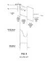
- FIG. 1is a partial cross-sectional view of an intermediate structure for a semiconductor device 100 having a semiconductor-oxide-nitride-oxide-semiconductor (SONOS) gate stack 102 including a conventional oxide-nitride-oxide (ONO) stack 104 formed over a surface 106 of a semiconductor substrate 108 according to a conventional method.
- the device 100typically further includes one or more diffusion regions 110 , such as source and drain regions, aligned to the gate stack and separated by a channel region 112 .
- the SONOS gate stack 102includes a poly-silicon (poly) gate layer 114 formed upon and in contact with the ONO stack 104 .
- the poly gate 114is separated or electrically isolated from the substrate 108 by the ONO stack 104 .
- the ONO stack 104generally includes a silicon oxide tunneling layer 116 , a silicon nitride charge trapping layer 118 which serves as a charge storing or memory layer for the device 100 , and a silicon oxide blocking layer 120 overlying the charge trapping layer 118 .
- Such SONOS-type transistorsare useful for non-volatile memory (NVM).
- the charge trapping layerstores charge to provide non-volatility.
- a positive voltageis applied to the control gate (V CG ) while the source, body and drain are grounded.
- V CGcontrol gate
- FIG. 2An energy band diagram, trapped charge distribution and trap density distribution of a conventional n-channel SONOS device having a channel 212 , oxide tunneling layer 216 , nitride memory layer 218 and oxide blocking layer 220 during programming is depicted in FIG. 2 .
- the positive V CGproduces a field across the SONOS stack resulting in some negative charge at the conduction band energy level in the buried channel of silicon substrate channel to undergo Fowler-Nordheim tunneling (FNT) through the tunneling layer and into the charge trapping layer.
- the electronsare stored in traps having mid gap energy levels in the charge trapping nitride.
- the trap density distributionis substantially uniform throughout the charge trapping layer.
- the trapped charge distributionis such that the majority of trapped charge is in the portion of the charge trapping layer (i.e. memory layer) proximate to the blocking oxide.
- a negative voltageis applied to the control gate 314 .
- FIG. 3An energy band diagram showing the channel 312 , oxide tunneling layer 316 , nitride memory layer 318 and oxide blocking layer 320 during erasing is depicted in FIG. 3 .
- the negative V CGproduces a field across the SONOS stack attracting hole tunneling charge through the tunneling layer and into the charge trapping layer.
- SONOS-type devicesare gaining in popularity for high density memory applications, such as embedded NVM. It is known in the industry that uniform channel Fowler-Nordheim tunneling (FNT) and/or direct tunneling (DT) for program and erase result in improved reliability over other methods. A combination of FNT and DT is referred to here and is referred to as modified Fowler-Nordheim tunneling (MFNT) Currently, conventional SONOS operate in the 10 V range for MFNT. However, an advantage of SONOS over other NVM devices is voltage scalability.
- FNTFowler-Nordheim tunneling
- DTdirect tunneling
- MFNTmodified Fowler-Nordheim tunneling
- SONOShas been theorized, with proper scaling, there exists potential in SONOS to achieve a memory technology operable in the 5 volt (V) range, rather than the 10 V range of conventional SONOS-type devices or 12 V-15 V range of conventional flash technology.
- V5 volt
- SONOS-type devices operable at low voltages (approaching 5 V)are advantageously compatible with low voltage CMOS.
- faster programming or erasingmay be possible at a particular voltage for a scaled device.
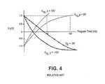
- successful scaling of SONOS-type devicesis non-trivial. For example, FIG.
- FIG. 4depicts programming and erase times for a conventional SONOS device employing a conventional ONO stack comprised of a 10 nm thick silicon dioxide blocking layer, a 7 nm thick silicon nitride charge trapping layer, and a 3 nm thick silicon dioxide tunneling layer.
- the programming/erase timeincreases dramatically when V CG is scaled down.
- program/erase times less than 1 msare desirable for embedded memory applications.
- 1 millisecond (ms) program/erase timesmay be achieved in the conventional SONOS stack only with a V CG of +/ ⁇ 10 V.
- Conventional SONOS program/erase timesextend to 100 ms or more when V CG is reduced to approximately +/ ⁇ 9 V.
- the programming voltageresults in a reduction of the erase or program window (i.e. memory window).
- the electric fieldis across the ONO stack is reduced if the equivalent oxide thickness (EOT) of the entire ONO stack is not scaled down as the voltage is reduced.
- EOTequivalent oxide thickness
- Reducing the EOT of the stackis non-trivial because reducing the tunneling layer thickness to allow the same initial erase level at a lower applied voltage (V CG ) can result in a detrimental increase in the erase and program decay rate
- V CGapplied voltage
- the charge trapping layer thicknessis reduced, the charge centroid is placed closer to the substrate, increasing charge loss to the substrate.
- the blocking oxide thicknessis scaled down, the electron reverse injection from the control gate is increased, causing damage to the ONO stack and data retention loss.
- Reverse injectionis manifested as further shown in FIG. 4 , where the FNT erase reaches “saturation.” This occurs when electrons are back streamed from the gate into the memory layer faster than they can be removed via hole transport across the tunnel oxide. Accordingly, there remains a need to scale the ONO stack of a SONOS device in a manner capable of providing a device operable at a lower program/erase voltage.
- FIG. 1illustrates a cross sectional view of an intermediate structure for a conventional SONOS device.
- FIG. 2depicts an energy band diagram, trapped charge distribution and trap density distribution of a conventional SONOS device during program.
- FIG. 3depicts an energy band diagram of a conventional SONOS device during erase.
- FIG. 4depicts programming and erase times for a conventional SONOS device employing a conventional ONO stack.
- FIG. 5illustrates a cross-sectional side view of a portion of a scaled nonvolatile trapped-charge memory device having a scaled ONO structure including a nitridized oxide tunneling layer, a multi-layer oxynitride charge trapping layer and a densified blocking layer according to an embodiment of the present invention.
- FIG. 6illustrates an approximate nitrogen concentration profile of the nitridized oxide tunneling layer in accordance with an embodiment of the present invention.
- FIG. 7Aillustrates a graph depicting simulation showing reduction in programming voltage attributable to a nitridized oxide tunneling layer in accordance with an embodiment of the present invention.
- FIG. 7Billustrates a comparison of two concentration profiles of hydrogen, nitrogen, oxygen, and silicon in a blocking layer, charge trapping layer and tunneling layer of two different SONOS-type devices.
- FIG. 8Adepicts a retention mode energy band diagram of a scaled SONOS-type device in accordance with an embodiment of the present invention.
- FIG. 8Bdepicts energy band diagram, trapped charge distribution and trap density distribution of a scaled SONOS-type device in accordance with an embodiment of the present invention during program.
- FIG. 9is a flow chart of a SONOS scaling method of fabricating a scaled ONO structure including a nitridized oxide tunneling layer, a multi-layer charge trapping layer and a reoxidized blocking layer according to an embodiment of the present invention.
- FIG. 10is a flow chart of a SONOS scaling method of forming a nitridized oxide tunneling layer.
- Embodiments of scaling a nonvolatile trapped-charge memory deviceare described herein with reference to figures. However, particular embodiments may be practiced without one or more of these specific details, or in combination with other known methods, materials, and apparatuses. In the following description, numerous specific details are set forth, such as specific materials, dimensions and processes parameters etc. to provide a thorough understanding of the present invention. In other instances, well-known semiconductor design and fabrication techniques have not been described in particular detail to avoid unnecessarily obscuring the present invention.
- Reference throughout this specification to “an embodiment”means that a particular feature, structure, material, or characteristic described in connection with the embodiment is included in at least one embodiment of the invention. Thus, the appearances of the phrase “in an embodiment” in various places throughout this specification are not necessarily referring to the same embodiment of the invention. Furthermore, the particular features, structures, materials, or characteristics may be combined in any suitable manner in one or more embodiments.
- Certain embodiments of the present inventioninclude a scaled SONOS-type device.
- the tunneling layer, charge trapping layer and blocking layerare modified to scale the SONOS-type device.
- the scaled SONOS deviceis operable at programming and erase voltages below +/ ⁇ 10 V.
- the scaled SONOS deviceis operated with an erase voltage between ⁇ 5 V and ⁇ 9V, and preferably between ⁇ 5 V and ⁇ 7 V, to provide an initial erase voltage threshold level (VTE) of ⁇ 1 to ⁇ 3 V and preferably ⁇ 2 to ⁇ 3 after a 1 ms-10 ms pulse when operated at temperature of between ⁇ 40 to 95 degrees Celsius (° C.).
- VTEinitial erase voltage threshold level
- the SONOS-type deviceis operated with a programming voltage between 5 V and 9V, and preferably between 5 V and 7 V, to provide an initial program voltage threshold level (VTP) of 1 V to 3 V, preferably 2 V to 3 V, after a 1 ms to 10 ms, preferably 5 ms, programming pulse.
- VTPinitial program voltage threshold level
- These exemplary scaled SONOS devicesproviding an end of life (EOL) memory window of between 1 V and 2 V after 20 years at 85° C. and at least 10,000 write/erase cycles, preferably 100,000 cycles.
- a conventional pure oxygen (oxide) tunneling layeris replaced with a nitridized oxide having a particular nitrogen concentration profile to reduce the equivalent oxide thickness of the tunneling layer relative to the pure oxygen tunneling layer while retaining low interface trap density.
- Thisenables reducing (scaling) the programming/erase voltages while providing an erase voltage threshold level (VTP/VTE) as good or better than a conventional, non-scaled device.
- the conventional charge trapping layer of nitrideis replaced with a multi-layer oxynitride film having at least a top and bottom layer of distinct stoichiometry.
- the multi-layer oxynitrideincludes a silicon-rich, oxygen-lean top layer to locate and confine the centroid of charge away from the tunnel oxide layer, thereby locally increasing trap density within the charge trapping layer.
- the conventional blocking layer of high temperature oxide (HTO)is replaced with a reoxidized blocking layer to density the blocking oxide and thereby reduce the memory decay rate with scaling.
- HTOhigh temperature oxide
- Such embodimentsprovide sufficient net charge for an adequate memory window while also reducing trap assisted tunneling to improve or maintain programming and erase threshold voltages (VTP/VTE) when the SONOS device is operated at a reduced program/erase voltage.
- the terms “over,” “under,” “between,” and “on” as used hereinrefer to a relative position of one layer with respect to other layers.
- one layer deposited or disposed over or under another layermay be directly in contact with the other layer or may have one or more intervening layers.
- one layer deposited or disposed between layersmay be directly in contact with the layers or may have one or more intervening layers.
- a first layer “on” a second layeris in contact with that second layer.
- the relative position of one layer with respect to other layersis provided assuming operations deposit, modify and remove films relative to a starting substrate without consideration of the absolute orientation of the substrate.
- the nonvolatile trapped-charge memory deviceis a SONOS-type device wherein a charge-trapping layer is an insulator layer, such as a nitride.
- the nonvolatile trapped-charge memory deviceis a Flash-type device wherein the charge-trapping layer is a conductor layer or a semiconductor layer, such as poly-silicon.
- Nonvolatile trapped-charge memory devices employing the nitridized oxide tunneling layermay enable a lower programming or erase voltage while providing an erase voltage threshold level (VTP/VTE) as good as or better than a conventional device.
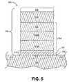
- FIG. 5illustrates a cross-sectional side view of an intermediate structure of a SONOS-type device 500 having a scaled ONO stack according to an embodiment of the present invention. It should be appreciated that various other SONOS embodiments disclosed herein may also be employed to produce a scaled ONO stack beyond the specific embodiment depicted in FIG. 5 , but nonetheless also operable at a reduced program/erase voltage. Thus, while the features of FIG. 5 may be referenced throughout the description, the present invention is not limited to this particular embodiment.
- the SONOS-type device 500includes a SONOS gate stack 502 including an ONO stack 504 formed over a surface 513 of a substrate 508 .
- SONOS-type device 500further includes one or more source and drain regions 510 , aligned to the gate stack 502 and separated by a channel region 512 .
- the scaled SONOS gate stack 502includes a gate layer 514 formed upon and in contact with the scaled ONO stack 504 and a portion of the substrate 508 .
- the gate layer 514is separated or electrically isolated from the substrate 508 by the scaled ONO stack 504 .
- substrate 508is a bulk substrate comprised of a single crystal of a material which may include, but is not limited to, silicon, germanium, silicon-germanium or a III-V compound semiconductor material.
- substrate 508is comprised of a bulk layer with a top epitaxial layer.
- the bulk layeris comprised of a single crystal of a material which may include, but is not limited to, silicon, germanium, silicon/germanium, a III-v compound semiconductor material and quartz, while the top epitaxial layer is comprised of a single crystal layer which may include, but is not limited to, silicon, germanium, silicon/germanium and a III-V compound semiconductor material.
- substrate 508is comprised of a top epitaxial layer on a middle insulator layer which is above a lower bulk layer.
- the top epitaxial layeris comprised of a single crystal layer which may include, but is not limited to, silicon (i.e. to form a silicon-on-insulator (SOD semiconductor substrate), germanium, silicon/germanium and a III-V compound semiconductor material.
- the insulator layeris comprised of a material which may include, but is not limited to, silicon dioxide, silicon nitride and silicon oxy-nitride.
- the lower bulk layeris comprised of a single crystal which may include, but is not limited to, silicon, germanium, silicon/germanium, a III-V compound semiconductor material and quartz.
- Substrate 508 and, hence, the channel region 512 between the source and drain regions 510may comprise dopant impurity atoms.
- the channel regionis doped P-type and, in an alternative embodiment, the channel region is doped N-type.
- Source and drain regions 510 in substrate 508may be any regions having opposite conductivity to the channel region 512 .
- source and drain regions 510are N-type doped while channel region 512 is P-type doped.
- substrate 508is comprised of boron-doped single-crystal silicon having a boron concentration in the range of 1 ⁇ 10 15 -1 ⁇ 10 19 atoms/cm 3 .
- Source and drain regions 510are comprised of phosphorous- or arsenic-doped regions having a concentration of N-type dopants in the range of 5 ⁇ 10 16 -5 ⁇ 10 19 atoms/cm 3 .
- source and drain regions 510have a depth in substrate 508 in the range of 80-200 nanometers.
- source and drain regions 510are P-type doped while the channel region of substrate 508 is N-type doped.
- the SONOS-type device 500further includes, over channel region 512 , a gate stack 502 including an ONO stack 504 , a gate layer 514 and a gate cap layer 525 .
- the ONO stack 504further includes tunneling layer 516 , a charge trapping layer 518 and a blocking layer 520 .
- the tunneling layer 516includes a nitridized oxide. Because programming and erase voltages produce large electric fields across a tunneling layer, on the order of 10 MV/cm, the program/erase tunneling current is more a function of the tunneling layer barrier height than the tunneling layer thickness. However, during retention, there is no large electric field present and so the loss of charge is more a function of the tunneling layer thickness than barrier height. To improve tunneling current for reduced operating voltages without sacrificing charge retention, in a particular embodiment, the tunneling layer 516 is a nitridized oxide. Nitridation increases the relative permittivity or dielectric constant ( ⁇ ) of the tunneling layer by inducing nitrogen to an otherwise pure silicon dioxide film.
- the tunneling layer 516 of nitridized oxidehas the same physical thickness as a conventional SONOS-type device employing pure oxygen tunnel oxide.
- nitridationprovides a tunnel layer with an effective ( ⁇ ) between 4.75 and 5.25, preferably between 4.90 and 5.1 (at standard temperature). In one such embodiment, nitridation provides a tunnel layer with an effective ( ⁇ ) of 5.07, at standard temperature.
- the nitridized tunnel oxide of the scaled SONOS devicehas the same physical thickness as a conventional, non-scaled SONOS device employing pure oxygen tunnel oxide.
- the higher permittivity of the nitridized tunnel oxideresults in the memory layer charging faster.
- the charge trapping layer 518charges during program/erase faster than a pure oxygen tunnel oxide of that thickness because relatively less of the large electric field from the control gate is dropped across the nitridized tunnel oxide (due to the relatively higher permittivity of nitridized tunnel oxide).
- the SONOS-type device 500allows the SONOS-type device 500 to operate with a reduced program/erase voltage while still achieving the same program/erase voltage threshold level (VTP/VTE) as a conventional SONOS-type device.
- the SONOS-type device 500employs a tunneling layer 516 having nitridized tunnel oxide with a physical thickness between 1.5 nm and 3.0 nm, and preferably between 1.9 nm and 2.2 nm.
- the tunneling layer 516is nitridized in a particular manner to reduce the trap density at the substrate interface to improve charge retention.
- charge retentionmay be approximately the same as the pure oxygen tunnel oxide of the same thickness. Referring to FIG. 6 , depicting an approximate nitrogen concentration profile within one embodiment of the tunneling layer 616 , the nitrogen concentration 614 decreases rapidly toward the substrate interface 613 to limit the formation of a silicon nitride (Si 3 N 4 ) layer in contact with the substrate 612 .
- a silicon nitride layercomprising polar molecules, detrimentally increases the trap density if present at the substrate interface 613 , thereby reducing charge retention via trap to trap tunneling.
- the programming/erase V CGmay be reduced without a significant reduction in charge retention of the scaled SONOS device.
- nitridization of oxide within the tunneling layerreduces its energy barrier and increases the dielectric constant relative to a pure oxide tunneling layer.
- tunneling layer 516is annotated for illustration purposes with a centerline 517 .
- FIG. 6depicts a similar centerline 617 with one half the thickness of the tunneling layer 616 proximate the substrate 612 and one half the thickness of the tunneling layer 616 proximate the charge trapping layer 618 .
- the nitrogen concentration 614is below 5 ⁇ 10 21 atoms/cm 3 throughout the first 25% of the thickness of the tunneling layer 616 and reaches approximately 5 ⁇ 10 21 atoms/cm 3 at 50% of the thickness of the tunneling layer 616 , or at the centerline 617 . In a further embodiment, the nitrogen concentration 614 is above 5 ⁇ 10 21 atoms/cm 3 within the last 25% of the thickness of the tunneling layer 616 , proximate the charge trapping layer 618 .
- the nitrogen concentration 614is below 5 ⁇ 10 21 atoms/cm 3 within the first 0.6 nm of the tunneling layer proximate the substrate 612 and is at least 5 ⁇ 10 21 atoms/cm 3 at 1.1 nm of the tunneling layer 616 thickness.
- the capacitance of the tunneling layermay be increased without a significant reduction in charge retention of a scaled SONOS-type device.
- FIG. 7illustrates a graph depicting a simulation showing a reduction in programming voltage attributable to a nitridized oxide tunneling layer in accordance with an embodiment of the present invention.
- leakage current at retention voltages for 20 ⁇ pure oxide tunneling layer and 40 ⁇ nitride charge trapping layeris equal to 20 ⁇ nitridized oxide tunneling layer and 40 ⁇ charge trapping layer nitride, while charging current for the nitridized oxide tunneling layer at programming voltages is greater than that of the pure oxide tunneling layer.
- a nitridized oxide tunneling layer in accordance with the present inventionmay provide the same program erase level achieved with a 10 V program or erase voltage and a conventional pure oxide tunneling layer.
- the charge trapping layer 518 of the SONOS-type device 500may further include any commonly known charge trapping material and have any thickness suitable to store charge and, modulate the threshold voltage of the device.
- charge trapping layer 518is silicon nitride (Si 3 N 4 ), silicon-rich silicon nitride, or silicon-rich silicon oxynitride.
- the silicon-rich filmincludes daggling silicon bonds.
- the charge trapping layer 518has a non-uniform stoichiometry across the thickness of charge trapping layer.
- the charge trapping layer 518may further include at least two oxynitride layers having differing compositions of silicon, oxygen and nitrogen.
- Such compositional nonhomogeneity within the charge trapping layerhas a number of performance advantages over a conventional SONOS charge trapping layer having a substantially homogeneous composition. For example, reducing the thickness of the conventional SONOS charge trapping layer increases the trap to trap tunneling rate, resulting in a loss of data retention. However, when the stoichiometry of the charge trapping layer is modified in accordance with an embodiment of the present invention, the thickness of the charge trapping layer may be scaled down while still maintaining good data retention.
- the bottom oxynitride layer 518 Aprovides a local region within the charge trapping layer having a relatively lower density of trap states, thereby reducing the trap density at the tunnel oxide interface to reduce trap assisted tunneling in the scaled SONOS device. This results in reduced stored charge loss for a given charge trapping layer thickness to enable scaling of the charge trapping layer for scaling of the ONO stack EOT.
- the bottom oxynitride 518 Ahas a first composition with a high silicon concentration, a high oxygen concentration and a low nitrogen concentration to provide an oxygen-rich oxynitride.
- This first oxynitridemay have a physical thickness between 2.5 nm and 4.0 nm corresponding to an EOT of between 1.5 nm and 5.0 nm.
- the bottom oxynitride layer 518 Ahas an effective dielectric constant ( ⁇ ) of approximately 6.
- a top oxynitride layer 518 Bprovides a local region within the charge trapping layer having a relatively higher density of trap states.
- the relatively higher density of trap statesenables a charge trapping layer of reduced thickness to provide sufficient trapped charge that the memory window remains adequate in the scaled ONO stack.
- the higher density of trap stateshas the effect of increasing the difference between programming and erase voltages of memory devices for a particular charge trapping layer thickness, allowing the charge trapping layer thickness to be reduced and thereby reducing the EOT of the ONO stack in the scaled SONOS device.
- the composition of the top oxynitride layerhas a high silicon concentration and a high nitrogen concentration with a low oxygen concentration to produce a silicon-rich, oxygen-lean oxynitride.
- the higher silicon content of the top oxynitridethe higher the density of trap states provided by the top oxynitride and the more the top oxynitride layer thickness can be reduced (thereby reducing the charge trapping layer thickness to enable lower voltage operation).
- the higher the silicon contentthe greater the permittivity and the lower the EOT for the top oxynitride layer.
- This reduction in EOTmay more than offset the increase in EOT of the oxygen-rich bottom oxynitride, for a net reduction in EOT of the charge trapping layer relative to conventional oxynitride charge trapping layers having a substantially homogeneous composition.
- the top oxynitridean effective dielectric constant of approximately 7.
- FIG. 7Bdepicts exemplary secondary ion mass spectroscopy (SIMS) profiles indicating the concentrations in atoms/cm 3 of silicon (Si), nitrogen (N), oxygen (O) and hydrogen (H) after deposition (as-deposited) of a tunneling layer, charge trapping layer, and blocking layer.
- SIMSsecondary ion mass spectroscopy
- a base line condition (“BL”) and a dual-layer oxynitride condition like that depicted in FIG. 5 (“Bilayer”)are overlaid.
- the baseline conditionhas a conventional charge trapping layer with a homogenous composition.
- the x-axisrepresents the depth with 0 nm being at the exposed top surface of the blocking layer and proceeding through the stack from top down, terminating in the substrate.
- the oxygen concentration for the Bilayer conditionis well below 1.0 ⁇ 10 22 atoms/cm 3 in the depth region between approximately 5 nm and 10 nm, corresponding to a portion of the charge trapping layer.
- the baseline conditiondisplays a substantially higher oxygen concentration of greater than 1.0 ⁇ 10 22 within this same region.
- the baseline conditionhas a substantially constant oxygen concentration between the 6 nm and 10 nm marks while the Bilayer condition shows substantially more oxygen near the 10 nm mark than the 6 nm mark. This non-uniformity in oxygen concentration represents the transition between the oxygen-lean top oxynitride and the oxygen-rich bottom oxynitride in the Bilayer condition.
- the ratio of the bottom oxynitride layer thickness to the top oxynitride layer thicknessis between 1:6 and 6:1, and more preferably at the ratio of bottom oxynitride thickness to top oxynitride thickness is at least 1:4.
- the first oxynitridehas a physical thickness between 2.5 nm and 4.0 nm
- the second oxynitride 518 Bhas a physical thickness between 5.0 nm and 6.0 nm for a charge trapping layer 518 with a net physical thickness of between 7.5 nm and 10.0 nm.
- the top oxynitrideemploying a bottom oxynitride with a physical thickness of 30 ⁇ , the top oxynitride has a physical thickness of 60 ⁇ for a scaled charge trapping layer with a net physical thickness of 90 ⁇ .
- compositional nonhomogeneityis utilized to both locate and confine traps to an embedded locale of the charge trapping layer (i.e. concentrate the traps) a distance from the tunnel layer interface.
- FIG. 8Afurther illustrates an energy band diagram during retention of a scaled SONOS device including a nitridized tunnel oxide 816 , a multi-layer charge trapping oxynitride 818 and a densified blocking layer 820 between a substrate 812 and control gate 814 according to an embodiment of the present invention.
- the nonhomogeneity in the composition of the charge trapping layer 818impacts both the valence and conduction bands between the silicon-rich top oxynitride 818 B and oxygen-rich bottom oxynitride 818 A of the charge trapping layer.
- the charge trapping layer in accordance with an embodiment the present inventionprovides a modulation in the bands at the interface of the oxygen-rich and silicon-rich oxynitride layers within the charge trapping layer 818 .
- This band gap modulationserves to locate the trapped charge centroid within the top oxynitride layer, further away from the substrate for a given charge trapping layer thickness.
- the conduction band modulation between the oxynitride layersmay also serve to reduce back streaming.
- a portion of the silicon-rich top oxynitride 818 Bis oxidized or reoxidized in a particular embodiment.
- Such an oxidation of the silicon-rich top regionmay produce a graded bandgap proximate to the blocking layer 820 relative to the pre-oxidation bandgap depicted as dashed lines for illustration purposes in FIG. 8A .
- approximately half of the top oxynitride layer 818 Bis reoxidized to have a higher oxygen concentration toward the interface with the blocking layer 820 .
- substantially all of the top oxynitride layer 818 Bis reoxidized to have a higher oxygen concentration than as-deposited.
- the reoxidationincreases the oxygen concentration in the top oxynitride layer 818 B by approximately 0.25 ⁇ 10 21 -0.35 ⁇ 10 21 atoms/cm 3 .
- Such embodiments employing a reoxidized charge trapping layermay prevent trap migration to the interface between the charge trapping layer and the blocking layer, thereby allowing the charge trapping layer thickness to be reduced without incurring the charge retention penalty associated with thinning a charge trapping layer of substantially homogeneous composition.
- Preventing the charge from migrating to the blocking oxide layeralso reduces the electric field across the blocking oxide during erase which reduces the back streaming of electrons, or to allow scaling down the blocking oxide while maintaining the same level of electron back streaming.
- Such trap location and confinement provided by the regions of distinct stoichiometry in the charge trapping layer and as further combined with reoxidation of a portion of the charge trapping layer in particular embodimentsmay enable a scaled SONOS device in accordance with the present invention to operate at a reduced voltage or with faster program and erase times while maintaining good memory retention.
- the multi-layer charge storing layercan include any number, n, of oxynitride layers, any or all of which having differing compositions of oxygen, nitrogen and/or silicon.
- multi-layer charge storing layers having up to five oxynitride layers of differing compositionshave been produced and tested.
- the blocking layer 520 of the ONO stack 504includes a layer of silicon dioxide between about 30 ⁇ and about 50 ⁇ . Scaling of the blocking layer 520 in the ONO stack of the SONOS-type device is non-trivial because if done improperly can detrimentally increase back streaming of carriers from the control gate under certain bias conditions.
- the blocking layer 520is a high temperature oxide (HTO) which is relatively denser than as-deposited. A densified oxide has a lower fraction of terminal hydrogen or hydroxyl bonds. For example, removal of the hydrogen or water from an HTO oxide has the effect of increasing the film density and improving the quality of the HTO oxide.
- HTOhigh temperature oxide
- the higher quality oxideenables the layer to be scaled in thickness.
- the hydrogen concentrationis greater than 2.5 ⁇ 10 20 atoms/cm 3 as deposited and is reduced to below 8.0 ⁇ 10 19 atoms/cm 3 in the densified film.
- the thickness of the HTO oxideis between 2.5 nm and 10.0 nm as-deposited and anywhere between 10% and 30% thinner upon densification.
- the blocking oxide layeris further modified to incorporate nitrogen.
- the nitrogenis incorporated in the form of an ONO stack across the thickness of the blocking oxide layer.
- Such a sandwich structure in place of the conventional pure oxygen blocking layeradvantageously reduces the EOT of the entire stack between the channel and control gate as well as enable tuning of band offsets to reduce back injection of carriers.
- the ONO block layercan then be incorporated with the nitridized tunnel oxide and charge trapping layer comprising a bottom oxynitride layer and a top oxynitride layer.
- the gate layer 514may be any conductor or semiconductor material.
- the gate layer 514is poly-silicon (poly).
- the gate layer 514contains a metal, such as, but not limited to, hafnium, zirconium, titanium, tantalum, aluminum, ruthenium, palladium, platinum, cobalt and nickel, their silicides, their nitrides and their carbides.
- the gate layer 514is poly-silicon having a physical thickness of between 70 nm and 250 nm.
- the SONOS-type device 500includes a gate cap layer 525 super adjacent to the gate layer 514 and has approximately the same critical dimensions as the gate layer 514 and ONO stack 504 .
- the gate cap layer 525forms the top layer of the gate stack 502 and provides a hard mask during patterning of the gate layer 514 and ONO stack 504 .
- the gate cap layer 525facilitates formation of self aligned contacts (SAC) to the SONOS devices.
- the gate cap layer 525may be comprised of any material capable providing the necessary selectivity to subsequent etch processes, such as, but not limited to, silicon dioxide, silicon nitride, and silicon oxynitride.
- a SONOS-type deviceemploys an ONO stack including a nitridized tunnel oxide with an EOT of 14 ⁇ corresponding to a physical thickness of approximately 18 ⁇ , a charge trapping layer comprising a bottom oxynitride layer with an EOT of 20 ⁇ corresponding to a physical thickness of approximately 25 ⁇ and a top oxynitride layer with an EOT of 30 ⁇ corresponding to a physical thickness of approximately 60 ⁇ , and a blocking oxide layer deposited to 40 ⁇ and densified to 30 ⁇ .
- Such a SONOS-type devicemay be operated at a voltage range of approximately 9 V, to provide an initial erase voltage threshold level (VTE) of ⁇ 2 V after a 1 ms to 10 ms pulse.
- VTEinitial erase voltage threshold level
- FIG. 9depicts a flow chart of a method for fabricating a scaled SONOS, such as that depicted in FIG. 5 , including a nitridized oxide tunneling layer, a multi-layer charge trapping oxynitride that has been partially reoxidized and a densified blocking oxide layer, as described above.
- the fabrication method of FIG. 9begins with forming a nitridized oxide tunneling layer over a silicon-containing surface of a substrate at operation 900 .
- FIG. 10depicts a flow chart of specific method for forming the nitridized oxide of operation 900 in FIG. 9 .
- a thin thermal oxideis formed from a silicon containing layer on a surface of a substrate, such as substrate 508 of FIG. 5 . Because a good interface with the substrate is necessary, formation of a chemical oxide may preface the thermal oxidation. In a particular embodiment, therefore, a chemical oxide is present during the thermal oxidation (as opposed to performing a conventional “HF last” pre-clean). In one such embodiment, the chemical oxide is grown with ozonated water to form a chemical oxide layer with a thickness of approximately 1.0 nm.
- the thermal oxideis formed to a thickness of between approximately 1.0 nm and 1.8 nm. In a particular embodiment, the thermal oxide is formed to a thickness of between 1.0 nm and 1.2 nm. Thus, in embodiments where a 1.0 nm chemical oxide is present during the thermal oxidation of operation 501 , the thickness of the surface oxide does not substantially increase, however the quality of the oxide is improved. In a further embodiment, the oxide is of relatively low density to facilitate subsequent incorporation of a significant wt % of nitrogen. Too low of a film density, however, will result in too much nitrogen at the silicon substrate interface. Formation of the silicon dioxide layer at operation 501 further serves as a means to block additional substrate oxide formation during subsequent thermal processing, discussed further below.
- an atmospheric pressure vertical thermal reactoris employed to grow the thermal oxide at a temperature between 680° C. and 800° C. in the presence of an oxidizing gas such as, oxygen (O 2 ), nitrous oxide (N 2 O), nitric oxide (NO), ozone (O 3 ), and steam (H 2 O).
- an oxidizing gassuch as, oxygen (O 2 ), nitrous oxide (N 2 O), nitric oxide (NO), ozone (O 3 ), and steam (H 2 O).
- the oxidation of operation 1001may be from 3.5 minutes to 20 minutes in duration.
- employing O 2 gas at a temperature between 700° C. and 750° C.a process time between 7 minutes and 20 minutes forms an approximately 1.0 nm silicon dioxide film.
- the oxidation operation 1001is performed with a sub-atmospheric processor such as the Advanced Vertical Processor (AVP) commercially available from AVIZA technology of Scotts Valley, Calif.
- AVPAdvanced Vertical Processor
- the AVPmay be operated in the temperature range described above for a VTR embodiment and at a pressure between 1 Torr (T) and atmospheric pressure.
- T1 Torr
- the oxidation time to form a thermal silicon dioxide film of between approximately 1.0 nm and 1.8 nm in thicknessmay extend up to nearly an hour, as may be determined by one of ordinary skill in the art.
- the thermal oxide formed at operation 1001is nitridized.
- a nitrogen annealis performed to increase the dielectric constant ( ⁇ ) and reduce the fixed charge of the thermal oxide layer.
- the nitrogen annealemploys nitrogen (N 2 ) or a hydrogenated nitrogen source, such as ammonia (NH 3 ).
- the nitrogen annealemploys a deuterated nitrogen source, such as deuterated ammonia (ND 3 ).
- the nitrogen annealis performed at a temperature between 700° C. and 850° C. for between 3.5 minutes and 30 minutes.
- the nitrogen annealis performed at a temperature between 725° C. and 775° C., for between 3.5 minutes and 30 minutes.
- NH 3is introduced at atmospheric pressure at a temperature of between 725° C. and 775° C., for between 3.5 minutes and 30 minutes.
- a sub-atmospheric NH 3 annealis performed at 800° C. to 900° C. for 5 minutes to 30 minutes in a processor such as the AVP.
- commonly known nitrogen plasma and thermal anneal combinationsare performed.
- a reoxidationis performed at operation 1004 .
- an oxidizing gasis thermally cracked to provide oxygen radicals close to the film surface.
- the oxygen radicalseliminate nitrogen and hydrogen trap charge.
- the reoxidation operation 1002also grows an additional oxide at the substrate interface to provide a physical offset between the substrate and a nitrogen concentration within the tunneling layer. For example, referring back to FIG. 5 , the reoxidation helps to separate the substrate interface 513 from a nitrogen concentration within the tunneling layer 516 . As specifically shown in FIG.
- the nitrogen concentration 614 in the tunneling layer 616 at the substrate interface 613is significantly below 5 ⁇ 10 21 atoms/cm 3 and may be on the order of 5 ⁇ 10 20 atoms/cm 3 .
- This offset in the nitrogen from the substrate interfaceimproves retention of a SONOS-type device.
- the thickness of the oxide grown at the substrate interface 613is limited to between 1.2 nm and 3.0 nm.
- the reoxidation process conditionsare chosen such that the thickness of the thermal oxide formed at operation 1001 prevents oxidation beyond a thickness of approximately 3.0 nm, which could render a tunneling layer devoid of any advantageous nitrogen concentration.
- oxidizersmay be employed for the reoxidation process, such as, but not limited to, NO, N 2 O, O 2 , O 3 and steam. Any such oxidizers may be introduced with known thermal processors operating at a temperature of between 800° C. and 850° C. Depending on the operating parameters, reoxidation time may be anywhere between 5 minutes and 40 minutes. In a particular embodiment, NO is employed in an atmospheric furnace operated at a temperature between 800° C. and 850° C. for a process time of approximately 15 minutes to form a nitridized oxide film that is approximately 2.2 nm in thickness on a silicon substrate.
- the reoxidized film 2.2 nm thickforms a region between 0.5 nm and 0.8 nm proximate to the interface with the silicon substrate, the region having a nitrogen concentration below 5 ⁇ 10 21 atoms/cm 3 .
- a second nitrogen annealis performed at operation 1006 to renitridize the tunneling layer.
- a second nitrogen annealis employed to further increase the dielectric constant of the tunneling layer without detrimentally introducing a large number of hydrogen or nitrogen traps at the substrate interface.
- the second nitrogen anneal of operation 1006is performed with conditions identical to the anneal performed in operation 1002 .
- the second nitrogen anneal of operation 1006is performed at a higher temperature than the first nitrogen anneal of operation 1002 to introduce additional nitrogen into the tunneling layer.
- the nitrogen annealemploys a hydrogenated nitrogen source, such as NH 3 .
- the nitrogen annealemploys a deuterated nitrogen source, such as ND 3 .
- the nitrogen anneal of operation 1006employs NH 3 at atmospheric pressure and a temperature between 750° C. and 950° C. with a processing time of between 3.5 minutes and 30 minutes.
- the NH 3 annealis performed at atmospheric pressure between 800° C. and 850° C. for between 5 minutes and 10 minutes.
- operations 1001 through 1006 depicted in FIG. 10provide two oxidation operations and two nitridation operations.
- the iterative oxidation, nitridation scheme depictedenables specific tailoring of the nitrogen concentration in the tunneling layer to achieve both a reduction in programming voltage or increase in programming speed and an increase in memory retention of a SONOS-type device.
- the successive nature of the oxidation, nitridation, reoxidation, renitridation operations 1001 - 1006enable an appreciable nitrogen concentration in a tunneling layer less than 3.0 nm thick while providing an interface between the tunneling layer and the substrate that has very little nitrogen and hydrogen traps.
- the independent oxidation, nitridation, reoxidation, renitridation operations 1001 - 1006enable the first and second oxidations and first and second nitridation to be performed with independently engineered conditions to provide greater degrees of freedom in tailoring the nitrogen concentration profile in a tunneling layer.
- operation 1001 , 1002 , 1004 and 1006are successively performed in a single thermal processor without removing the substrate from the processor between operations.
- process pressureis held at atmosphere for operations 1001 - 1006 .
- oxidation operation 1001is performed at a temperature of between 700° C. and 750° C. Gas flows are then modified as prescribed to perform the nitrogen anneal of operation 1002 at a temperature between 725° C.
- furnace temperatureis then ramped up to between 800° C. and 850° C. and gas flows are again modified to perform the reoxidation of operation 1004 .
- gas flowsare again modified to perform the second nitrogen anneal of operation 1006 .
- nitridized oxide tunneling layer 516 of FIG. 5fabrication of the ONO stack may continue by returning to the method depicted in FIG. 9 .
- multiple nitride or oxynitride charge trapping layersare formed at operations 902 and 904 in a low pressure CVD process using a silicon source, such as silane (SiH 4 ), dichlorosilane (SiH 2 Cl 2 ), tetrachlorosilane (SiCl 4 ) or Bis-TertiaryButylAmino Silane (BTBAS), a nitrogen source, such as N 2 , NH 3 , N 2 O or nitrogen trioxide (NO 3 ), and an oxygen-containing gas, such as O 2 or N 2 O.
- a silicon sourcesuch as silane (SiH 4 ), dichlorosilane (SiH 2 Cl 2 ), tetrachlorosilane (SiCl 4 ) or Bis-TertiaryButylAmino Si
- gases in which-hydrogen has been replaced by deuteriumcan be used, including, for example, the substitution of ND 3 for NH 3 .
- the substitution of deuterium for hydrogenadvantageously passivates Si dangling bonds at the substrate interface, thereby increasing an NBTI (Negative Bias Temperature Instability) lifetime of SONOS-type devices.
- an oxynitride charge trapping layercan be deposited at operation 902 over a tunneling layer by placing the substrate in a deposition chamber and introducing a process gas including N 2 O, NH 3 and DCS, while maintaining the chamber at a pressure of from about 5 millitorr (mT) to about 500 mT, and maintaining the substrate at a temperature of from about 700° C. to about 850° C. and more preferably at least about 780° C., for a period of from about 2.5 minutes to about 20 minutes.
- mTmillitorr
- the process gascan include a first gas mixture of N 2 O and NH 3 mixed in a ratio of from about 8:1 to about 1:8 and a second gas mixture of SiH 2 Cl 2 and NH 3 mixed in a ratio of from about 1:7 to about 7:1, and can be introduced at a flow rate of from about 5 to about 200 standard cubic centimeters per minute (sccm). It has been found that an oxynitride layer produced or deposited under these condition yields a silicon-rich oxygen-rich, oxynitride layer, such as the charge trapping layer 518 A depicted in FIG. 5 .
- Formation of the charge trapping layermay further involve a CVD process at operation 904 employing a first gas mixture of N 2 O and NH 3 mixed in a ratio of from about 8:1 to about 1:8 and a second gas mixture of SiH 2 Cl 2 and NH 3 mixed in a ratio of from about 1:7 to about 7:1, introduced at a flow rate of from about 5 to about 20 sccm to yield a silicon-rich, nitrogen-rich, and oxygen-lean oxynitride layer, such as the charge trapping layer 518 B depicted in FIG. 5 .
- formation of a charge trapping layer at operations 902 and 904is performed sequentially in the same processing tool used to form the tunneling layer without unloading the substrate from the deposition chamber between operations 901 and 904 .
- the charge trapping layeris deposited without altering the temperature at which the substrate was heated during the second nitrogen anneal of operation 1006 of FIG. 10 .
- the charge trapping layeris deposited sequentially and immediately following nitridation of the tunneling layer at operation 901 by modifying the flow rate of NH 3 gas, and introducing N2O and SiH 2 Cl 2 to provide the desired gas ratios to yield either a silicon-rich and oxygen-rich layer, a silicon-rich and nitrogen-rich oxynitride layer, or both layers in a dual-layer implementation.
- a blocking layercan be formed at operation 906 by any suitable means including, for example, thermal oxidation or deposition with CVD techniques.
- the blocking layeris formed with a high-temperature CVD process.
- the deposition processinvolves providing a silicon source, such as SiH 4 , SiH 2 Cl 2 , or SiCl 4 and an oxygen-containing gas, such as O 2 or N 2 O in a deposition chamber at a pressure of from about 50 mT to about 1000 mT, for a period of from about 10 minutes to about 120 minutes while maintaining the substrate at a temperature of from about 650° C. to about 850° C.
- the blocking layeris deposited sequentially in the same processing tool employed to form the charge trapping layer(s) at operations 902 and 904 . More preferably, the blocking layer is formed in the same processing tool as is both the charge trapping layer(s) and the tunneling layer without removing the substrate between operations.
- the blocking layer deposited at operation 906is reoxidized at operation 908 to density the blocking layer oxide.
- operation 908may further oxidize or reoxidize a portion or all of the charge trapping layer, such as a portion or all of the charge trapping layer 518 B shown in FIG. 5 to achieve a graded band gap, such as depicted in FIG. 8A .
- the reoxidationmay be performed in the presence of an oxidizing gas such as, oxygen (O 2 ), nitrous oxide (N 2 O), nitric oxide (NO), ozone (O 3 ), and steam (H 2 O).
- the reoxidation processmay is performed at a higher temperature than the temperature at which the blocking layer is deposited. Reoxidation after the deposition of the blocking oxide enables a more controlled diffusion of oxidizer to controllably oxidize or reoxidize the thin charge trapping layer.
- a dilute wet oxidationis employed. The dilute wet oxidation is distinct from a wet oxidation in that the H 2 :O 2 ratio is between 1 and 1.3. In one specific embodiment, a dilute oxidation with an H 2 :O 2 ratio of approximately 1.2 is performed at a temperature of between 800° C. and 900° C.
- the duration of the dilute oxidationmay be sufficient to grow between 5.0 nm and 12.5 nm of silicon dioxide on a silicon substrate. In one such embodiment, the duration is sufficient to for an approximately 10 nm to 1.1 nm silicon dioxide layer on a silicon substrate.
- Such a dilute oxidation processserves to reoxidize the deposited blocking layer oxide and may further oxidize or reoxidize a portion of the charge trapping layer to impart a band structure like that depicted in FIG. 8A or 8 B.
- the reoxidation of operation 908may further serve to form a gate oxide in a non-SONOS-type device region, such as for a complementary metal oxide silicon (CMOS) field effect transistors (FET), on the same substrate as the SONOS-type device.
- CMOScomplementary metal oxide silicon
- FETfield effect transistors
- the reoxidation of operation 908may further serve to diffuse deuterium into portions of the charge trapping layer or blocking layer of the SONOS-type device.
- the methodmay then be completed at operation 910 with formation of a gate layer, such as the gate layer 514 of FIG. 5 .
- operation 910may further include formation of a gate cap layer, such as gate cap layer 525 depicted in FIG. 5 .
- further processingmay occur as known in the art to conclude fabrication of the SONOS-type device 300 .
Landscapes
- Non-Volatile Memory (AREA)
- Semiconductor Memories (AREA)
Abstract
Description
Claims (13)
Priority Applications (9)
| Application Number | Priority Date | Filing Date | Title |
|---|---|---|---|
| US11/904,506US8614124B2 (en) | 2007-05-25 | 2007-09-26 | SONOS ONO stack scaling |
| PCT/US2007/020966WO2008147386A1 (en) | 2007-05-25 | 2007-09-28 | Sonos ono stack scaling |
| CN2007800359633ACN101517714B (en) | 2007-05-25 | 2007-09-28 | SONOS ONO stack shrinks proportionally |
| TW096136630ATWI436455B (en) | 2007-05-25 | 2007-09-29 | Semiconductor-Oxide-Nitride-Oxide-Semiconductor (SONOS) Oxide-Nitride-Oxide (ONO) Stacking Scaling |
| US13/539,461US9299568B2 (en) | 2007-05-25 | 2012-07-01 | SONOS ONO stack scaling |
| US15/051,279US9997641B2 (en) | 2007-05-25 | 2016-02-23 | SONOS ONO stack scaling |
| US15/988,981US10699901B2 (en) | 2007-05-25 | 2018-05-24 | SONOS ONO stack scaling |
| US16/914,904US20210104402A1 (en) | 2007-05-25 | 2020-06-29 | Sonos ono stack scaling |
| US17/970,345US20230074163A1 (en) | 2007-05-25 | 2022-10-20 | Sonos ono stack scaling |
Applications Claiming Priority (2)
| Application Number | Priority Date | Filing Date | Title |
|---|---|---|---|
| US94038407P | 2007-05-25 | 2007-05-25 | |
| US11/904,506US8614124B2 (en) | 2007-05-25 | 2007-09-26 | SONOS ONO stack scaling |
Related Child Applications (1)
| Application Number | Title | Priority Date | Filing Date |
|---|---|---|---|
| US13/539,461Continuation-In-PartUS9299568B2 (en) | 2007-05-25 | 2012-07-01 | SONOS ONO stack scaling |
Publications (2)
| Publication Number | Publication Date |
|---|---|
| US20080290400A1 US20080290400A1 (en) | 2008-11-27 |
| US8614124B2true US8614124B2 (en) | 2013-12-24 |
Family
ID=40071593
Family Applications (3)
| Application Number | Title | Priority Date | Filing Date |
|---|---|---|---|
| US11/904,506Active2031-06-02US8614124B2 (en) | 2007-05-25 | 2007-09-26 | SONOS ONO stack scaling |
| US12/005,813Active2029-05-08US8637921B2 (en) | 2007-05-25 | 2007-12-27 | Nitridation oxidation of tunneling layer for improved SONOS speed and retention |
| US14/166,608ActiveUS9349877B1 (en) | 2007-05-25 | 2014-01-28 | Nitridation oxidation of tunneling layer for improved SONOS speed and retention |
Family Applications After (2)
| Application Number | Title | Priority Date | Filing Date |
|---|---|---|---|
| US12/005,813Active2029-05-08US8637921B2 (en) | 2007-05-25 | 2007-12-27 | Nitridation oxidation of tunneling layer for improved SONOS speed and retention |
| US14/166,608ActiveUS9349877B1 (en) | 2007-05-25 | 2014-01-28 | Nitridation oxidation of tunneling layer for improved SONOS speed and retention |
Country Status (4)
| Country | Link |
|---|---|
| US (3) | US8614124B2 (en) |
| CN (1) | CN101517714B (en) |
| TW (1) | TWI436455B (en) |
| WO (1) | WO2008147386A1 (en) |
Cited By (9)
| Publication number | Priority date | Publication date | Assignee | Title |
|---|---|---|---|---|
| US20130001673A1 (en)* | 2010-03-22 | 2013-01-03 | Micron Technology, Inc. | Fortification of charge storing material in high k dielectric environments and resulting apparatuses |
| US8883624B1 (en)* | 2013-09-27 | 2014-11-11 | Cypress Semiconductor Corporation | Integration of a memory transistor into high-K, metal gate CMOS process flow |
| US9023707B1 (en) | 2009-04-24 | 2015-05-05 | Cypress Semiconductor Corporation | Simultaneously forming a dielectric layer in MOS and ONO device regions |
| US9299568B2 (en) | 2007-05-25 | 2016-03-29 | Cypress Semiconductor Corporation | SONOS ONO stack scaling |
| US9349877B1 (en) | 2007-05-25 | 2016-05-24 | Cypress Semiconductor Corporation | Nitridation oxidation of tunneling layer for improved SONOS speed and retention |
| US10497711B2 (en) | 2016-07-27 | 2019-12-03 | Sandisk Technologies Llc | Non-volatile memory with reduced program speed variation |
| US10615289B2 (en) | 2007-12-12 | 2020-04-07 | Longitude Flash Memory Solutions Ltd. | Nonvolatile charge trap memory device having a high dielectric constant blocking region |
| US10700083B1 (en) | 2009-04-24 | 2020-06-30 | Longitude Flash Memory Solutions Ltd. | Method of ONO integration into logic CMOS flow |
| US10720444B2 (en) | 2018-08-20 | 2020-07-21 | Sandisk Technologies Llc | Three-dimensional flat memory device including a dual dipole blocking dielectric layer and methods of making the same |
Families Citing this family (38)
| Publication number | Priority date | Publication date | Assignee | Title |
|---|---|---|---|---|
| US8643124B2 (en) | 2007-05-25 | 2014-02-04 | Cypress Semiconductor Corporation | Oxide-nitride-oxide stack having multiple oxynitride layers |
| US8063434B1 (en) | 2007-05-25 | 2011-11-22 | Cypress Semiconductor Corporation | Memory transistor with multiple charge storing layers and a high work function gate electrode |
| US8633537B2 (en) | 2007-05-25 | 2014-01-21 | Cypress Semiconductor Corporation | Memory transistor with multiple charge storing layers and a high work function gate electrode |
| US20090179253A1 (en) | 2007-05-25 | 2009-07-16 | Cypress Semiconductor Corporation | Oxide-nitride-oxide stack having multiple oxynitride layers |
| US9449831B2 (en) | 2007-05-25 | 2016-09-20 | Cypress Semiconductor Corporation | Oxide-nitride-oxide stack having multiple oxynitride layers |
| US8940645B2 (en) | 2007-05-25 | 2015-01-27 | Cypress Semiconductor Corporation | Radical oxidation process for fabricating a nonvolatile charge trap memory device |
| US20090152621A1 (en)* | 2007-12-12 | 2009-06-18 | Igor Polishchuk | Nonvolatile charge trap memory device having a high dielectric constant blocking region |
| JP5238332B2 (en)* | 2008-04-17 | 2013-07-17 | 株式会社東芝 | Manufacturing method of semiconductor device |
| US20100052037A1 (en)* | 2008-08-28 | 2010-03-04 | Albert Chin | Charge-trapping engineered flash non-volatile memory |
| JP4902716B2 (en)* | 2008-11-20 | 2012-03-21 | 株式会社日立国際電気 | Nonvolatile semiconductor memory device and manufacturing method thereof |
| CN106653761A (en)* | 2009-04-10 | 2017-05-10 | 赛普拉斯半导体公司 | Oxide-nitride-oxide stack comprising multi-layer oxynitride layer |
| US20110101442A1 (en) | 2009-11-02 | 2011-05-05 | Applied Materials, Inc. | Multi-Layer Charge Trap Silicon Nitride/Oxynitride Layer Engineering with Interface Region Control |
| US8343839B2 (en) | 2010-05-27 | 2013-01-01 | International Business Machines Corporation | Scaled equivalent oxide thickness for field effect transistor devices |
| US8524614B2 (en)* | 2010-11-29 | 2013-09-03 | International Business Machines Corporation | III-V compound semiconductor material passivation with crystalline interlayer |
| TWI534897B (en)* | 2011-01-14 | 2016-05-21 | 賽普拉斯半導體公司 | Oxide-nitride-oxide stack with multiple oxynitride layers |
| US8772057B1 (en) | 2011-05-13 | 2014-07-08 | Cypress Semiconductor Corporation | Inline method to monitor ONO stack quality |
| US8772059B2 (en)* | 2011-05-13 | 2014-07-08 | Cypress Semiconductor Corporation | Inline method to monitor ONO stack quality |
| CN102446964B (en)* | 2011-11-08 | 2015-08-19 | 上海华力微电子有限公司 | By the ONO structure and preparation method thereof of DPN silicon oxynitride as SONOS storage medium layer |
| US8836009B2 (en)* | 2011-12-01 | 2014-09-16 | National Chiao Tung University | Flash memory |
| US20130168754A1 (en)* | 2011-12-28 | 2013-07-04 | Macronix International Co., Ltd. | Method for fabricating a semiconductor device with increased reliability |
| US8685813B2 (en) | 2012-02-15 | 2014-04-01 | Cypress Semiconductor Corporation | Method of integrating a charge-trapping gate stack into a CMOS flow |
| US8980711B2 (en)* | 2012-02-28 | 2015-03-17 | Taiwan Semiconductor Manufacturing Company, Ltd. | Memory device structure and method |
| EP2831918A4 (en)* | 2012-03-29 | 2015-11-18 | Cypress Semiconductor Corp | ONO INTEGRATION METHOD IN LOGICAL CMOS FLOW |
| CN104769721A (en)* | 2012-07-01 | 2015-07-08 | 赛普拉斯半导体公司 | SONOS ONO Stack Improvements |
| KR102146640B1 (en)* | 2012-07-01 | 2020-08-21 | 롱지튜드 플래쉬 메모리 솔루션즈 리미티드 | Radical oxidation process for fabricating a nonvolatile charge trap memory device |
| US9378821B1 (en) | 2013-01-18 | 2016-06-28 | Cypress Semiconductor Corporation | Endurance of silicon-oxide-nitride-oxide-silicon (SONOS) memory cells |
| US8796098B1 (en)* | 2013-02-26 | 2014-08-05 | Cypress Semiconductor Corporation | Embedded SONOS based memory cells |
| US9331184B2 (en) | 2013-06-11 | 2016-05-03 | United Microelectronics Corp. | Sonos device and method for fabricating the same |
| CN104779208A (en)* | 2014-01-13 | 2015-07-15 | 上海华虹宏力半导体制造有限公司 | Method for improving time storage efficiency of ONO structure in SONOS flash memory |
| US9412596B1 (en)* | 2015-01-30 | 2016-08-09 | International Business Machines Corporation | Nitridation on HDP oxide before high-k deposition to prevent oxygen ingress |
| US10128265B2 (en) | 2017-01-18 | 2018-11-13 | Micron Technology, Inc. | Memory cells, integrated structures and memory arrays |
| JP6876500B2 (en)* | 2017-04-19 | 2021-05-26 | ルネサスエレクトロニクス株式会社 | Manufacturing method of semiconductor devices |
| JP2019054068A (en)* | 2017-09-13 | 2019-04-04 | 東芝メモリ株式会社 | Semiconductor storage device and method for manufacturing the same |
| CN109166861B (en)* | 2018-09-12 | 2020-11-24 | 长江存储科技有限责任公司 | A kind of three-dimensional memory and its production method |
| US10741253B1 (en)* | 2019-02-20 | 2020-08-11 | Sandisk Technologies Llc | Memory device with compensation for erase speed variations due to blocking oxide layer thinning |
| JP7189814B2 (en)* | 2019-03-18 | 2022-12-14 | キオクシア株式会社 | semiconductor storage device |
| CN111403396B (en)* | 2020-01-14 | 2021-11-23 | 长江存储科技有限责任公司 | Channel structure including tunneling layer with adjusted nitrogen weight percentage and method of forming the same |
| US20230101604A1 (en)* | 2021-09-24 | 2023-03-30 | Intel Corporation | Three-dimensional memory devices with transition metal dichalcogenide (tmd) channels |
Citations (70)
| Publication number | Priority date | Publication date | Assignee | Title |
|---|---|---|---|---|
| US4395438A (en) | 1980-09-08 | 1983-07-26 | Amdahl Corporation | Low pressure chemical vapor deposition of silicon nitride films |
| US4543707A (en) | 1983-06-30 | 1985-10-01 | Kabushiki Kaisha | Method of forming through holes by differential etching of stacked silicon oxynitride layers |
| US5817170A (en) | 1993-06-22 | 1998-10-06 | Ceram Incorporated | Low temperature seeding process for ferroelectric memory device |
| US5972765A (en) | 1997-07-16 | 1999-10-26 | International Business Machines Corporation | Use of deuterated materials in semiconductor processing |
| US6015739A (en) | 1997-10-29 | 2000-01-18 | Advanced Micro Devices | Method of making gate dielectric for sub-half micron MOS transistors including a graded dielectric constant |
| US6136654A (en) | 1996-06-07 | 2000-10-24 | Texas Instruments Incorporated | Method of forming thin silicon nitride or silicon oxynitride gate dielectrics |
| US6153543A (en) | 1999-08-09 | 2000-11-28 | Lucent Technologies Inc. | High density plasma passivation layer and method of application |
| US6157426A (en) | 1998-02-13 | 2000-12-05 | Ois Optical Imaging Systems, Inc. | Liquid crystal display with SiOx Ny inclusive multilayer black matrix |
| US6214689B1 (en) | 1998-03-02 | 2001-04-10 | Samsung Electronics Co., Ltd. | Apparatus for manufacturing semiconductor device, method of manufacturing capacitor of semiconductor device thereby, and resultant capacitor |
| US6218700B1 (en) | 1997-10-29 | 2001-04-17 | Stmicroelectronics S.A. | Remanent memory device |
| US6297096B1 (en) | 1997-06-11 | 2001-10-02 | Saifun Semiconductors Ltd. | NROM fabrication method |
| US6321134B1 (en) | 1997-07-29 | 2001-11-20 | Silicon Genesis Corporation | Clustertool system software using plasma immersion ion implantation |
| US6365518B1 (en) | 2001-03-26 | 2002-04-02 | Applied Materials, Inc. | Method of processing a substrate in a processing chamber |
| US6433383B1 (en) | 1999-07-20 | 2002-08-13 | Advanced Micro Devices, Inc. | Methods and arrangements for forming a single interpoly dielectric layer in a semiconductor device |
| US6445030B1 (en) | 2001-01-30 | 2002-09-03 | Advanced Micro Devices, Inc. | Flash memory erase speed by fluorine implant or fluorination |
| US6444521B1 (en) | 2000-11-09 | 2002-09-03 | Macronix International Co., Ltd. | Method to improve nitride floating gate charge trapping for NROM flash memory device |
| US6461899B1 (en) | 1999-04-30 | 2002-10-08 | Semiconductor Energy Laboratory, Co., Ltd. | Oxynitride laminate “blocking layer” for thin film semiconductor devices |
| US20020154878A1 (en) | 2001-02-09 | 2002-10-24 | Akwani Ikerionwu A. | High germanium content waveguide materials |
| US6518113B1 (en) | 2001-02-06 | 2003-02-11 | Advanced Micro Devices, Inc. | Doping of thin amorphous silicon work function control layers of MOS gate electrodes |
| US20030123307A1 (en) | 2001-12-27 | 2003-07-03 | Samsung Electronics Co., Ltd. | Non-volatile memory device and a method of fabricating the same |
| US20030124873A1 (en) | 2001-12-28 | 2003-07-03 | Guangcai Xing | Method of annealing an oxide film |
| US6610614B2 (en)* | 2001-06-20 | 2003-08-26 | Texas Instruments Incorporated | Method for uniform nitridization of ultra-thin silicon dioxide layers in transistor gates |
| US20030183869A1 (en)* | 2002-01-31 | 2003-10-02 | Stmicroelectronics S.R.I. | Manufacturing process of an interpoly dielectric structure for non-volatile semiconductor integrated memories |
| US6677213B1 (en) | 2002-03-08 | 2004-01-13 | Cypress Semiconductor Corp. | SONOS structure including a deuterated oxide-silicon interface and method for making the same |
| US6709928B1 (en) | 2001-07-31 | 2004-03-23 | Cypress Semiconductor Corporation | Semiconductor device having silicon-rich layer and method of manufacturing such a device |
| US20040094793A1 (en) | 2002-11-15 | 2004-05-20 | Mitsuhiro Noguchi | Semiconductor memory device |
| US20040104424A1 (en) | 1997-11-18 | 2004-06-03 | Semiconductor Energy Laboratory Co., Ltd. | Nonvolatile memory and electronic apparatus |
| US6746968B1 (en) | 2003-02-12 | 2004-06-08 | Macronix International Co., Ltd. | Method of reducing charge loss for nonvolatile memory |
| US20040183122A1 (en) | 2003-01-31 | 2004-09-23 | Renesas Technology Corp. | Nonvolatile semiconductor memory device |
| US20040207002A1 (en) | 2003-01-09 | 2004-10-21 | Samsung Electronics Co., Ltd. | SONOS memory device having side gate stacks and method of manufacturing the same |
| US6835621B2 (en) | 2002-07-10 | 2004-12-28 | Samsung Electronics Co., Ltd. | Method of fabricating non-volatile memory device having a structure of silicon-oxide-nitride-oxide-silicon |
| US20050026637A1 (en) | 2003-07-30 | 2005-02-03 | Fischer Michael Andrew | Intelligent downstream traffic delivery to multi-protocol stations |
| US20050070126A1 (en) | 2003-04-21 | 2005-03-31 | Yoshihide Senzaki | System and method for forming multi-component dielectric films |
| US20050186741A1 (en) | 2004-02-20 | 2005-08-25 | Tower Semiconductor Ltd. | SONOS embedded memory with CVD dielectric |
| US6958511B1 (en) | 2003-10-06 | 2005-10-25 | Fasl, Llc | Flash memory device and method of fabrication thereof including a bottom oxide layer with two regions with different concentrations of nitrogen |
| US20050236679A1 (en) | 2004-01-06 | 2005-10-27 | Fujitsu Limited | Semiconductor device, and method and apparatus for manufacturing the same |
| US20050245034A1 (en)* | 2002-06-28 | 2005-11-03 | National Institute Of Advanced Indust Sci& Tech | Semiconductor device and its manufacturing method |
| US20050266637A1 (en) | 2004-06-01 | 2005-12-01 | Macronix International Co., Ltd. | Tunnel oxynitride in flash memories |
| US20050275010A1 (en) | 2004-06-10 | 2005-12-15 | Hung-Wei Chen | Semiconductor nano-wire devices and methods of fabrication |
| US7018868B1 (en) | 2004-02-02 | 2006-03-28 | Advanced Micro Devices, Inc. | Disposable hard mask for memory bitline scaling |
| US20060065919A1 (en)* | 2004-09-29 | 2006-03-30 | Sony Corporation | Nonvolatile memory device and method for producing the same |
| US20060081331A1 (en) | 2003-10-15 | 2006-04-20 | Campian Jonathon R | Apparatus and method for holding materials for the forming and joining thereof |
| US7033957B1 (en) | 2003-02-05 | 2006-04-25 | Fasl, Llc | ONO fabrication process for increasing oxygen content at bottom oxide-substrate interface in flash memory devices |
| US20060111805A1 (en) | 1993-07-15 | 2006-05-25 | Renesas Technology Corp. | Fabrication system and fabrication method |
| US20060113627A1 (en) | 2004-11-29 | 2006-06-01 | Chung-I Chen | High-voltage transistor device having an interlayer dielectric etch stop layer for preventing leakage and improving breakdown voltage |
| US20060113586A1 (en)* | 2004-11-29 | 2006-06-01 | Macronix International Co., Ltd. | Charge trapping dielectric structure for non-volatile memory |
| US20060192248A1 (en) | 2004-10-19 | 2006-08-31 | Macronix International Co., Ltd. | Memory Device and Method of Manufacturing Including Deuterated Oxynitride Charge Trapping Structure |
| US7112486B2 (en) | 2004-07-06 | 2006-09-26 | Hynix Semiconductor Inc. | Method for fabricating semiconductor device by using radical oxidation |
| US7115469B1 (en) | 2001-12-17 | 2006-10-03 | Spansion, Llc | Integrated ONO processing for semiconductor devices using in-situ steam generation (ISSG) process |
| US20060228899A1 (en) | 2002-08-30 | 2006-10-12 | Fujitsu Amd Semiconductor Limited | Semiconductor memory device and method for manufacturing semiconductor device |
| US20060261401A1 (en) | 2005-05-17 | 2006-11-23 | Micron Technology, Inc. | Novel low power non-volatile memory and gate stack |
| US20070048916A1 (en) | 2005-08-23 | 2007-03-01 | Fujitsu Limited | Method for fabricating semiconductor device |
| US20070051306A1 (en) | 2002-11-19 | 2007-03-08 | Ivanov Igor C | Spatially-arranged chemical processing station |
| US20070121380A1 (en) | 2005-07-05 | 2007-05-31 | Mammen Thomas | Location-specific nand (ls nand) memory technology and cells |
| US20070210371A1 (en) | 2006-03-13 | 2007-09-13 | Renesas Technology Corp. | Nonvolatile semiconductor memory device and its fabrication method |
| US20070272971A1 (en) | 2003-05-28 | 2007-11-29 | Chang-Hyun Lee | Non-Volatile Memory Device and Method of Fabricating the Same |
| US20080029399A1 (en) | 2006-02-28 | 2008-02-07 | Fujifilm Corporation | Method of manufacturing nanostructures |
| US20080048237A1 (en) | 2006-07-26 | 2008-02-28 | Kabushiki Kaisha Toshiba | Nonvolatile semiconductor memory device |
| US20080146042A1 (en) | 2000-05-15 | 2008-06-19 | Asm International N.V. | Method of growing electrical conductors |
| US20080258203A1 (en) | 2007-04-19 | 2008-10-23 | Thomas Happ | Stacked sonos memory |
| US7450423B2 (en) | 2007-01-03 | 2008-11-11 | Macronix International Co., Ltd. | Methods of operating non-volatile memory cells having an oxide/nitride multilayer insulating structure |
| US20080290398A1 (en) | 2007-05-25 | 2008-11-27 | Igor Polishchuk | Nonvolatile charge trap memory device having <100> crystal plane channel orientation |
| US20080293207A1 (en) | 2007-05-25 | 2008-11-27 | Koutny Jr William W C | Integration of non-volatile charge trap memory devices and logic cmos devices |
| US20080293255A1 (en) | 2007-05-25 | 2008-11-27 | Krishnaswamy Ramkumar | Radical oxidation process for fabricating a nonvolatile charge trap memory device |
| US7482236B2 (en) | 2006-01-06 | 2009-01-27 | Taiwan Semiconductor Manufacturing Company, Ltd. | Structure and method for a sidewall SONOS memory device |
| US20090179253A1 (en) | 2007-05-25 | 2009-07-16 | Cypress Semiconductor Corporation | Oxide-nitride-oxide stack having multiple oxynitride layers |
| US20100252877A1 (en) | 2009-04-06 | 2010-10-07 | Toshiro Nakanishi | Non-Volatile Semiconductor Memory Devices Having Charge Trap Layers Between Word Lines and Active Regions Thereof |
| US8008713B2 (en) | 2005-11-28 | 2011-08-30 | International Business Machines Corporation | Vertical SOI trench SONOS cell |
| US8063434B1 (en) | 2007-05-25 | 2011-11-22 | Cypress Semiconductor Corporation | Memory transistor with multiple charge storing layers and a high work function gate electrode |
| US8067284B1 (en) | 2007-05-25 | 2011-11-29 | Cypress Semiconductor Corporation | Oxynitride bilayer formed using a precursor inducing a high charge trap density in a top layer of the bilayer |
Family Cites Families (107)
| Publication number | Priority date | Publication date | Assignee | Title |
|---|---|---|---|---|
| US4667217A (en) | 1985-04-19 | 1987-05-19 | Ncr Corporation | Two bit vertically/horizontally integrated memory cell |
| US4843023A (en) | 1985-09-25 | 1989-06-27 | Hewlett-Packard Company | Process for forming lightly-doped-drain (LDD) without extra masking steps |
| FR2683337B1 (en) | 1991-10-31 | 1994-01-07 | Bendix Europe Services Technique | PRESSURE REGULATING DEVICE FOR HYDRAULIC CIRCUIT. |
| JP3236706B2 (en)* | 1993-07-30 | 2001-12-10 | 三菱電機株式会社 | Nonvolatile semiconductor memory device and method of manufacturing the same |
| US5405791A (en) | 1994-10-04 | 1995-04-11 | Micron Semiconductor, Inc. | Process for fabricating ULSI CMOS circuits using a single polysilicon gate layer and disposable spacers |
| US5573963A (en) | 1995-05-03 | 1996-11-12 | Vanguard International Semiconductor Corporation | Method of forming self-aligned twin tub CMOS devices |
| KR0166840B1 (en) | 1995-05-12 | 1999-01-15 | 문정환 | Semiconductor device having a recess channel structure |
| EP0801427A3 (en) | 1996-04-11 | 1999-05-06 | Matsushita Electric Industrial Co., Ltd. | Field effect transistor, semiconductor storage device, method of manufacturing the same and method of driving semiconductor storage device |
| US5793089A (en) | 1997-01-10 | 1998-08-11 | Advanced Micro Devices, Inc. | Graded MOS transistor junction formed by aligning a sequence of implants to a selectively removable polysilicon sidewall space and oxide thermally grown thereon |
| TW577129B (en)* | 1997-03-05 | 2004-02-21 | Hitachi Ltd | Method for fabricating semiconductor integrated circuit device |
| US6469343B1 (en) | 1998-04-02 | 2002-10-22 | Nippon Steel Corporation | Multi-level type nonvolatile semiconductor memory device |
| US6475927B1 (en)* | 1998-02-02 | 2002-11-05 | Micron Technology, Inc. | Method of forming a semiconductor device |
| US6093606A (en) | 1998-03-05 | 2000-07-25 | Taiwan Semiconductor Manufacturing Company | Method of manufacture of vertical stacked gate flash memory device |
| US6001713A (en)* | 1998-09-16 | 1999-12-14 | Advanced Micro Devices, Inc. | Methods for forming nitrogen-rich regions in a floating gate and interpoly dielectric layer in a non-volatile semiconductor memory device |
| JP2000200842A (en) | 1998-11-04 | 2000-07-18 | Sony Corp | Nonvolatile semiconductor memory device, manufacturing method and writing method |
| JP3955409B2 (en) | 1999-03-17 | 2007-08-08 | 株式会社ルネサステクノロジ | Semiconductor memory device |
| JP4586219B2 (en) | 1999-09-17 | 2010-11-24 | ソニー株式会社 | Erase method for nonvolatile semiconductor memory device |
| US6949787B2 (en) | 2001-08-10 | 2005-09-27 | Spinnaker Semiconductor, Inc. | Transistor having high dielectric constant gate insulating layer and source and drain forming Schottky contact with substrate |
| US6597047B2 (en)* | 2000-03-22 | 2003-07-22 | Matsushita Electric Industrial Co., Ltd. | Method for fabricating a nonvolatile semiconductor device |
| DE10038877A1 (en)* | 2000-08-09 | 2002-02-28 | Infineon Technologies Ag | Memory cell and manufacturing process |
| US6479339B2 (en) | 2000-10-10 | 2002-11-12 | Texas Instruments Incorporated | Use of a thin nitride spacer in a split gate embedded analog process |
| JP4151229B2 (en) | 2000-10-26 | 2008-09-17 | ソニー株式会社 | Nonvolatile semiconductor memory device and manufacturing method thereof |
| US6610615B1 (en)* | 2000-11-15 | 2003-08-26 | Intel Corporation | Plasma nitridation for reduced leakage gate dielectric layers |
| US7075121B2 (en)* | 2000-12-20 | 2006-07-11 | Yamaha Corporation | Magnetic tunneling junction element having thin composite oxide film |
| US7151017B2 (en)* | 2001-01-26 | 2006-12-19 | Semiconductor Energy Laboratory Co., Ltd. | Method of manufacturing semiconductor device |
| JP4282248B2 (en)* | 2001-03-30 | 2009-06-17 | 株式会社東芝 | Semiconductor memory device |
| JP4091265B2 (en)* | 2001-03-30 | 2008-05-28 | 株式会社東芝 | Semiconductor device and manufacturing method thereof |
| US6429081B1 (en) | 2001-05-17 | 2002-08-06 | Taiwan Semiconductor Manufacturing Company | Parasitic surface transfer transistor cell (PASTT cell) for bi-level and multi-level NAND flash memory |
| KR100437453B1 (en) | 2002-05-23 | 2004-06-23 | 삼성전자주식회사 | NAND-type non-volatile memory device having SONOS gate structure and method of forming the same |
| US6991987B1 (en)* | 2002-11-27 | 2006-01-31 | Advanced Micro Devices, Inc. | Method for producing a low defect homogeneous oxynitride |
| JP2004193178A (en) | 2002-12-06 | 2004-07-08 | Fasl Japan 株式会社 | Semiconductor storage device and its manufacturing method |
| US6794764B1 (en) | 2003-03-05 | 2004-09-21 | Advanced Micro Devices, Inc. | Charge-trapping memory arrays resistant to damage from contact hole information |
| US7179754B2 (en)* | 2003-05-28 | 2007-02-20 | Applied Materials, Inc. | Method and apparatus for plasma nitridation of gate dielectrics using amplitude modulated radio-frequency energy |
| US7211864B2 (en) | 2003-09-15 | 2007-05-01 | Seliskar John J | Fully-depleted castellated gate MOSFET device and method of manufacture thereof |
| KR100586647B1 (en) | 2003-10-06 | 2006-06-07 | 동부일렉트로닉스 주식회사 | Flash memory device and manufacturing method thereof |
| KR100579844B1 (en) | 2003-11-05 | 2006-05-12 | 동부일렉트로닉스 주식회사 | Nonvolatile Memory Device and Manufacturing Method Thereof |
| KR100618815B1 (en) | 2003-11-12 | 2006-08-31 | 삼성전자주식회사 | Semiconductor device having heterogeneous gate insulating film and manufacturing method thereof |
| US7183166B2 (en) | 2003-11-25 | 2007-02-27 | Macronix International Co., Ltd. | Method for forming oxide on ONO structure |
| US7091089B2 (en) | 2004-06-25 | 2006-08-15 | Freescale Semiconductor, Inc. | Method of forming a nanocluster charge storage device |
| US7091130B1 (en) | 2004-06-25 | 2006-08-15 | Freescale Semiconductor, Inc. | Method of forming a nanocluster charge storage device |
| US7297597B2 (en) | 2004-07-23 | 2007-11-20 | Promos Technologies, Inc. | Method for simultaneously fabricating ONO-type memory cell, and gate dielectrics for associated high voltage write transistors and gate dielectrics for low voltage logic transistors by using ISSG |
| US6946349B1 (en) | 2004-08-09 | 2005-09-20 | Chartered Semiconductor Manufacturing Ltd. | Method for integrating a SONOS gate oxide transistor into a logic/analog integrated circuit having several gate oxide thicknesses |
| KR100583969B1 (en) | 2004-08-13 | 2006-05-26 | 삼성전자주식회사 | Manufacturing method of nonvolatile memory device having partial sono gate structure |
| US7393733B2 (en) | 2004-12-01 | 2008-07-01 | Amberwave Systems Corporation | Methods of forming hybrid fin field-effect transistor structures |
| US7642585B2 (en) | 2005-01-03 | 2010-01-05 | Macronix International Co., Ltd. | Non-volatile memory cells, memory arrays including the same and methods of operating cells and arrays |
| US8264028B2 (en) | 2005-01-03 | 2012-09-11 | Macronix International Co., Ltd. | Non-volatile memory cells, memory arrays including the same and methods of operating cells and arrays |
| US7315474B2 (en) | 2005-01-03 | 2008-01-01 | Macronix International Co., Ltd | Non-volatile memory cells, memory arrays including the same and methods of operating cells and arrays |
| US7473589B2 (en) | 2005-12-09 | 2009-01-06 | Macronix International Co., Ltd. | Stacked thin film transistor, non-volatile memory devices and methods for fabricating the same |
| US8482052B2 (en) | 2005-01-03 | 2013-07-09 | Macronix International Co., Ltd. | Silicon on insulator and thin film transistor bandgap engineered split gate memory |
| KR100644405B1 (en) | 2005-03-31 | 2006-11-10 | 삼성전자주식회사 | Gate Structure of Nonvolatile Memory Device and Manufacturing Method Thereof |
| US20060226500A1 (en) | 2005-04-06 | 2006-10-12 | Po-Lun Cheng | Gate dielectric layer and method of forming the same |
| KR100644397B1 (en)* | 2005-04-07 | 2006-11-10 | 삼성전자주식회사 | Thin film processing method and manufacturing method of nonvolatile memory cell using same |
| US7816728B2 (en) | 2005-04-12 | 2010-10-19 | International Business Machines Corporation | Structure and method of fabricating high-density trench-based non-volatile random access SONOS memory cells for SOC applications |
| US7279740B2 (en) | 2005-05-12 | 2007-10-09 | Micron Technology, Inc. | Band-engineered multi-gated non-volatile memory device with enhanced attributes |
| US7636257B2 (en) | 2005-06-10 | 2009-12-22 | Macronix International Co., Ltd. | Methods of operating p-channel non-volatile memory devices |
| US7402850B2 (en) | 2005-06-21 | 2008-07-22 | Micron Technology, Inc. | Back-side trapped non-volatile memory device |
| US7352018B2 (en) | 2005-07-22 | 2008-04-01 | Infineon Technologies Ag | Non-volatile memory cells and methods for fabricating non-volatile memory cells |
| JP5032056B2 (en)* | 2005-07-25 | 2012-09-26 | 株式会社東芝 | Method for manufacturing nonvolatile semiconductor memory device |
| JP2007043147A (en)* | 2005-07-29 | 2007-02-15 | Samsung Electronics Co Ltd | Method for forming silicon-rich nanocrystal structure using atomic layer deposition process and method for manufacturing nonvolatile semiconductor device using the same |
| US20070049048A1 (en)* | 2005-08-31 | 2007-03-01 | Shahid Rauf | Method and apparatus for improving nitrogen profile during plasma nitridation |
| US7429767B2 (en) | 2005-09-01 | 2008-09-30 | Micron Technology, Inc. | High performance multi-level non-volatile memory device |
| KR100697291B1 (en) | 2005-09-15 | 2007-03-20 | 삼성전자주식회사 | Nonvolatile Semiconductor Memory Device and Manufacturing Method Thereof |
| KR100719219B1 (en) | 2005-09-20 | 2007-05-16 | 동부일렉트로닉스 주식회사 | Manufacturing Method of Semiconductor Device |
| JP2009514194A (en) | 2005-09-23 | 2009-04-02 | エヌエックスピー ビー ヴィ | Storage element having improved performance and method for manufacturing such storage element |
| US20070087503A1 (en) | 2005-10-17 | 2007-04-19 | Saifun Semiconductors, Ltd. | Improving NROM device characteristics using adjusted gate work function |
| US8022465B2 (en) | 2005-11-15 | 2011-09-20 | Macronrix International Co., Ltd. | Low hydrogen concentration charge-trapping layer structures for non-volatile memory |
| US7678662B2 (en) | 2005-12-13 | 2010-03-16 | Applied Materials, Inc. | Memory cell having stressed layers |
| DE102006001680B3 (en) | 2006-01-12 | 2007-08-09 | Infineon Technologies Ag | Manufacturing method for a FinFET transistor arrangement and corresponding FinFET transistor arrangement |
| US7439594B2 (en) | 2006-03-16 | 2008-10-21 | Micron Technology, Inc. | Stacked non-volatile memory with silicon carbide-based amorphous silicon thin film transistors |
| US7859026B2 (en) | 2006-03-16 | 2010-12-28 | Spansion Llc | Vertical semiconductor device |
| US7948799B2 (en) | 2006-05-23 | 2011-05-24 | Macronix International Co., Ltd. | Structure and method of sub-gate NAND memory with bandgap engineered SONOS devices |
| KR100755410B1 (en) | 2006-09-22 | 2007-09-04 | 삼성전자주식회사 | Gate structure and method for forming same, nonvolatile memory device and method for manufacturing same |
| US8772858B2 (en) | 2006-10-11 | 2014-07-08 | Macronix International Co., Ltd. | Vertical channel memory and manufacturing method thereof and operating method using the same |
| US7651915B2 (en) | 2006-10-12 | 2010-01-26 | Infineon Technologies Ag | Strained semiconductor device and method of making same |
| US7811887B2 (en) | 2006-11-02 | 2010-10-12 | Saifun Semiconductors Ltd. | Forming silicon trench isolation (STI) in semiconductor devices self-aligned to diffusion |
| US7646041B2 (en) | 2006-12-04 | 2010-01-12 | Samsung Electronics Co., Ltd. | Non-volatile memory devices including vertical channels, methods of operating, and methods of fabricating the same |
| US20080150003A1 (en) | 2006-12-20 | 2008-06-26 | Jian Chen | Electron blocking layers for electronic devices |
| JP4772656B2 (en) | 2006-12-21 | 2011-09-14 | 株式会社東芝 | Nonvolatile semiconductor memory |
| US7811886B2 (en) | 2007-02-06 | 2010-10-12 | Freescale Semiconductor, Inc. | Split-gate thin film storage NVM cell with reduced load-up/trap-up effects |
| US20080237694A1 (en) | 2007-03-27 | 2008-10-02 | Michael Specht | Integrated circuit, cell, cell arrangement, method for manufacturing an integrated circuit, method for manufacturing a cell, memory module |
| KR100894098B1 (en) | 2007-05-03 | 2009-04-20 | 주식회사 하이닉스반도체 | Nonvolatile memory device having a fast erase speed and improved retention characteristics and method of manufacturing the same |
| US8643124B2 (en) | 2007-05-25 | 2014-02-04 | Cypress Semiconductor Corporation | Oxide-nitride-oxide stack having multiple oxynitride layers |
| US8680601B2 (en) | 2007-05-25 | 2014-03-25 | Cypress Semiconductor Corporation | Nonvolatile charge trap memory device having a deuterated layer in a multi-layer charge-trapping region |
| US7670963B2 (en) | 2007-05-25 | 2010-03-02 | Cypress Semiconductor Corportion | Single-wafer process for fabricating a nonvolatile charge trap memory device |
| US8614124B2 (en) | 2007-05-25 | 2013-12-24 | Cypress Semiconductor Corporation | SONOS ONO stack scaling |
| US9299568B2 (en) | 2007-05-25 | 2016-03-29 | Cypress Semiconductor Corporation | SONOS ONO stack scaling |
| DE102007025342B4 (en) | 2007-05-31 | 2011-07-28 | Globalfoundries Inc. | Higher transistor performance of N-channel transistors and P-channel transistors by using an additional layer over a double-stress layer |
| US7737488B2 (en) | 2007-08-09 | 2010-06-15 | Macronix International Co., Ltd. | Blocking dielectric engineered charge trapping memory cell with high speed erase |
| TW200913162A (en) | 2007-09-11 | 2009-03-16 | Univ Nat Chiao Tung | Nonvolatile memory device with nanowire channel and a method for fabricating the same |
| US20090086548A1 (en) | 2007-10-02 | 2009-04-02 | Eon Silicon Solution, Inc. | Flash memory |
| KR100880228B1 (en) | 2007-10-17 | 2009-01-28 | 주식회사 동부하이텍 | Manufacturing method of SONOS semiconductor device |
| KR101226685B1 (en) | 2007-11-08 | 2013-01-25 | 삼성전자주식회사 | Vertical type semiconductor device and Method of manufacturing the same |
| WO2009072983A1 (en) | 2007-12-07 | 2009-06-11 | Agency For Science, Technology And Research | Memory cell and methods of manufacturing thereof |
| US9431549B2 (en) | 2007-12-12 | 2016-08-30 | Cypress Semiconductor Corporation | Nonvolatile charge trap memory device having a high dielectric constant blocking region |
| US20090152621A1 (en) | 2007-12-12 | 2009-06-18 | Igor Polishchuk | Nonvolatile charge trap memory device having a high dielectric constant blocking region |
| US8120095B2 (en) | 2007-12-13 | 2012-02-21 | International Business Machines Corporation | High-density, trench-based non-volatile random access SONOS memory SOC applications |
| US8722484B2 (en) | 2008-01-14 | 2014-05-13 | Tower Semiconductor Ltd. | High-K dielectric stack and method of fabricating same |
| KR100975912B1 (en) | 2008-02-15 | 2010-08-13 | 한양대학교 산학협력단 | Multi-bit nonvolatile memory device and method of operating the device |
| KR100950477B1 (en) | 2008-03-05 | 2010-03-31 | 주식회사 하이닉스반도체 | Method for manufacturing nonvolatile memory device having charge trap layer |
| US8163660B2 (en) | 2008-05-15 | 2012-04-24 | Cypress Semiconductor Corporation | SONOS type stacks for nonvolatile change trap memory devices and methods to form the same |
| JP5356005B2 (en) | 2008-12-10 | 2013-12-04 | 株式会社東芝 | Nonvolatile semiconductor memory device and manufacturing method thereof |
| KR101573697B1 (en) | 2009-02-11 | 2015-12-02 | 삼성전자주식회사 | Nonvolatile memory device having vertical folding structure and method of fabricating the same |
| US8071453B1 (en) | 2009-04-24 | 2011-12-06 | Cypress Semiconductor Corporation | Method of ONO integration into MOS flow |
| US8222688B1 (en) | 2009-04-24 | 2012-07-17 | Cypress Semiconductor Corporation | SONOS stack with split nitride memory layer |
| KR101756227B1 (en) | 2010-08-13 | 2017-07-10 | 삼성전자 주식회사 | Semiconductor Device Comprising Vertical Channel Pattern |
| KR20120029291A (en) | 2010-09-16 | 2012-03-26 | 삼성전자주식회사 | Semiconductor devices and methods of fabricating the same |
| JP5172920B2 (en) | 2010-09-16 | 2013-03-27 | 株式会社東芝 | Nonvolatile semiconductor memory device |
- 2007
- 2007-09-26USUS11/904,506patent/US8614124B2/enactiveActive
- 2007-09-28WOPCT/US2007/020966patent/WO2008147386A1/enactiveApplication Filing
- 2007-09-28CNCN2007800359633Apatent/CN101517714B/enactiveActive
- 2007-09-29TWTW096136630Apatent/TWI436455B/enactive
- 2007-12-27USUS12/005,813patent/US8637921B2/enactiveActive
- 2014
- 2014-01-28USUS14/166,608patent/US9349877B1/enactiveActive
Patent Citations (78)
| Publication number | Priority date | Publication date | Assignee | Title |
|---|---|---|---|---|
| US4395438A (en) | 1980-09-08 | 1983-07-26 | Amdahl Corporation | Low pressure chemical vapor deposition of silicon nitride films |
| US4543707A (en) | 1983-06-30 | 1985-10-01 | Kabushiki Kaisha | Method of forming through holes by differential etching of stacked silicon oxynitride layers |
| US5817170A (en) | 1993-06-22 | 1998-10-06 | Ceram Incorporated | Low temperature seeding process for ferroelectric memory device |
| US20060111805A1 (en) | 1993-07-15 | 2006-05-25 | Renesas Technology Corp. | Fabrication system and fabrication method |
| US6136654A (en) | 1996-06-07 | 2000-10-24 | Texas Instruments Incorporated | Method of forming thin silicon nitride or silicon oxynitride gate dielectrics |
| US6297096B1 (en) | 1997-06-11 | 2001-10-02 | Saifun Semiconductors Ltd. | NROM fabrication method |
| US5972765A (en) | 1997-07-16 | 1999-10-26 | International Business Machines Corporation | Use of deuterated materials in semiconductor processing |
| US6321134B1 (en) | 1997-07-29 | 2001-11-20 | Silicon Genesis Corporation | Clustertool system software using plasma immersion ion implantation |
| US6015739A (en) | 1997-10-29 | 2000-01-18 | Advanced Micro Devices | Method of making gate dielectric for sub-half micron MOS transistors including a graded dielectric constant |
| US6218700B1 (en) | 1997-10-29 | 2001-04-17 | Stmicroelectronics S.A. | Remanent memory device |
| US20040104424A1 (en) | 1997-11-18 | 2004-06-03 | Semiconductor Energy Laboratory Co., Ltd. | Nonvolatile memory and electronic apparatus |
| US6157426A (en) | 1998-02-13 | 2000-12-05 | Ois Optical Imaging Systems, Inc. | Liquid crystal display with SiOx Ny inclusive multilayer black matrix |
| US6214689B1 (en) | 1998-03-02 | 2001-04-10 | Samsung Electronics Co., Ltd. | Apparatus for manufacturing semiconductor device, method of manufacturing capacitor of semiconductor device thereby, and resultant capacitor |
| US6461899B1 (en) | 1999-04-30 | 2002-10-08 | Semiconductor Energy Laboratory, Co., Ltd. | Oxynitride laminate “blocking layer” for thin film semiconductor devices |
| US6433383B1 (en) | 1999-07-20 | 2002-08-13 | Advanced Micro Devices, Inc. | Methods and arrangements for forming a single interpoly dielectric layer in a semiconductor device |
| US6153543A (en) | 1999-08-09 | 2000-11-28 | Lucent Technologies Inc. | High density plasma passivation layer and method of application |
| US20080146042A1 (en) | 2000-05-15 | 2008-06-19 | Asm International N.V. | Method of growing electrical conductors |
| US6444521B1 (en) | 2000-11-09 | 2002-09-03 | Macronix International Co., Ltd. | Method to improve nitride floating gate charge trapping for NROM flash memory device |
| US6445030B1 (en) | 2001-01-30 | 2002-09-03 | Advanced Micro Devices, Inc. | Flash memory erase speed by fluorine implant or fluorination |
| US6518113B1 (en) | 2001-02-06 | 2003-02-11 | Advanced Micro Devices, Inc. | Doping of thin amorphous silicon work function control layers of MOS gate electrodes |
| US20020154878A1 (en) | 2001-02-09 | 2002-10-24 | Akwani Ikerionwu A. | High germanium content waveguide materials |
| US6768856B2 (en) | 2001-02-09 | 2004-07-27 | Corning Incorporated | High germanium content waveguide materials |
| US6365518B1 (en) | 2001-03-26 | 2002-04-02 | Applied Materials, Inc. | Method of processing a substrate in a processing chamber |
| US6610614B2 (en)* | 2001-06-20 | 2003-08-26 | Texas Instruments Incorporated | Method for uniform nitridization of ultra-thin silicon dioxide layers in transistor gates |
| US6709928B1 (en) | 2001-07-31 | 2004-03-23 | Cypress Semiconductor Corporation | Semiconductor device having silicon-rich layer and method of manufacturing such a device |
| US7115469B1 (en) | 2001-12-17 | 2006-10-03 | Spansion, Llc | Integrated ONO processing for semiconductor devices using in-situ steam generation (ISSG) process |
| US20030123307A1 (en) | 2001-12-27 | 2003-07-03 | Samsung Electronics Co., Ltd. | Non-volatile memory device and a method of fabricating the same |
| US6774433B2 (en) | 2001-12-27 | 2004-08-10 | Samsung Electronics Co., Ltd. | Non-volatile memory device with diffusion layer |
| US20030124873A1 (en) | 2001-12-28 | 2003-07-03 | Guangcai Xing | Method of annealing an oxide film |
| US20030183869A1 (en)* | 2002-01-31 | 2003-10-02 | Stmicroelectronics S.R.I. | Manufacturing process of an interpoly dielectric structure for non-volatile semiconductor integrated memories |
| US6677213B1 (en) | 2002-03-08 | 2004-01-13 | Cypress Semiconductor Corp. | SONOS structure including a deuterated oxide-silicon interface and method for making the same |
| US20050245034A1 (en)* | 2002-06-28 | 2005-11-03 | National Institute Of Advanced Indust Sci& Tech | Semiconductor device and its manufacturing method |
| US6835621B2 (en) | 2002-07-10 | 2004-12-28 | Samsung Electronics Co., Ltd. | Method of fabricating non-volatile memory device having a structure of silicon-oxide-nitride-oxide-silicon |
| US20060228899A1 (en) | 2002-08-30 | 2006-10-12 | Fujitsu Amd Semiconductor Limited | Semiconductor memory device and method for manufacturing semiconductor device |
| US20040094793A1 (en) | 2002-11-15 | 2004-05-20 | Mitsuhiro Noguchi | Semiconductor memory device |
| US20070051306A1 (en) | 2002-11-19 | 2007-03-08 | Ivanov Igor C | Spatially-arranged chemical processing station |
| US20040207002A1 (en) | 2003-01-09 | 2004-10-21 | Samsung Electronics Co., Ltd. | SONOS memory device having side gate stacks and method of manufacturing the same |
| US20040183122A1 (en) | 2003-01-31 | 2004-09-23 | Renesas Technology Corp. | Nonvolatile semiconductor memory device |
| US7033957B1 (en) | 2003-02-05 | 2006-04-25 | Fasl, Llc | ONO fabrication process for increasing oxygen content at bottom oxide-substrate interface in flash memory devices |
| US6746968B1 (en) | 2003-02-12 | 2004-06-08 | Macronix International Co., Ltd. | Method of reducing charge loss for nonvolatile memory |
| US20050070126A1 (en) | 2003-04-21 | 2005-03-31 | Yoshihide Senzaki | System and method for forming multi-component dielectric films |
| US20070272971A1 (en) | 2003-05-28 | 2007-11-29 | Chang-Hyun Lee | Non-Volatile Memory Device and Method of Fabricating the Same |
| US20050026637A1 (en) | 2003-07-30 | 2005-02-03 | Fischer Michael Andrew | Intelligent downstream traffic delivery to multi-protocol stations |
| US6958511B1 (en) | 2003-10-06 | 2005-10-25 | Fasl, Llc | Flash memory device and method of fabrication thereof including a bottom oxide layer with two regions with different concentrations of nitrogen |
| US20060081331A1 (en) | 2003-10-15 | 2006-04-20 | Campian Jonathon R | Apparatus and method for holding materials for the forming and joining thereof |
| US20050236679A1 (en) | 2004-01-06 | 2005-10-27 | Fujitsu Limited | Semiconductor device, and method and apparatus for manufacturing the same |
| US7018868B1 (en) | 2004-02-02 | 2006-03-28 | Advanced Micro Devices, Inc. | Disposable hard mask for memory bitline scaling |
| US20050186741A1 (en) | 2004-02-20 | 2005-08-25 | Tower Semiconductor Ltd. | SONOS embedded memory with CVD dielectric |
| US20050266637A1 (en) | 2004-06-01 | 2005-12-01 | Macronix International Co., Ltd. | Tunnel oxynitride in flash memories |
| US20050275010A1 (en) | 2004-06-10 | 2005-12-15 | Hung-Wei Chen | Semiconductor nano-wire devices and methods of fabrication |
| US7112486B2 (en) | 2004-07-06 | 2006-09-26 | Hynix Semiconductor Inc. | Method for fabricating semiconductor device by using radical oxidation |
| US20060065919A1 (en)* | 2004-09-29 | 2006-03-30 | Sony Corporation | Nonvolatile memory device and method for producing the same |
| US20060192248A1 (en) | 2004-10-19 | 2006-08-31 | Macronix International Co., Ltd. | Memory Device and Method of Manufacturing Including Deuterated Oxynitride Charge Trapping Structure |
| US20060113586A1 (en)* | 2004-11-29 | 2006-06-01 | Macronix International Co., Ltd. | Charge trapping dielectric structure for non-volatile memory |
| US20060113627A1 (en) | 2004-11-29 | 2006-06-01 | Chung-I Chen | High-voltage transistor device having an interlayer dielectric etch stop layer for preventing leakage and improving breakdown voltage |
| US20060261401A1 (en) | 2005-05-17 | 2006-11-23 | Micron Technology, Inc. | Novel low power non-volatile memory and gate stack |
| US20070121380A1 (en) | 2005-07-05 | 2007-05-31 | Mammen Thomas | Location-specific nand (ls nand) memory technology and cells |
| US20070048916A1 (en) | 2005-08-23 | 2007-03-01 | Fujitsu Limited | Method for fabricating semiconductor device |
| US8008713B2 (en) | 2005-11-28 | 2011-08-30 | International Business Machines Corporation | Vertical SOI trench SONOS cell |
| US7482236B2 (en) | 2006-01-06 | 2009-01-27 | Taiwan Semiconductor Manufacturing Company, Ltd. | Structure and method for a sidewall SONOS memory device |
| US20080029399A1 (en) | 2006-02-28 | 2008-02-07 | Fujifilm Corporation | Method of manufacturing nanostructures |
| US20070210371A1 (en) | 2006-03-13 | 2007-09-13 | Renesas Technology Corp. | Nonvolatile semiconductor memory device and its fabrication method |
| US20080048237A1 (en) | 2006-07-26 | 2008-02-28 | Kabushiki Kaisha Toshiba | Nonvolatile semiconductor memory device |
| US7450423B2 (en) | 2007-01-03 | 2008-11-11 | Macronix International Co., Ltd. | Methods of operating non-volatile memory cells having an oxide/nitride multilayer insulating structure |
| US20080258203A1 (en) | 2007-04-19 | 2008-10-23 | Thomas Happ | Stacked sonos memory |
| US8067284B1 (en) | 2007-05-25 | 2011-11-29 | Cypress Semiconductor Corporation | Oxynitride bilayer formed using a precursor inducing a high charge trap density in a top layer of the bilayer |
| US20080296664A1 (en) | 2007-05-25 | 2008-12-04 | Krishnaswamy Ramkumar | Integration of non-volatile charge trap memory devices and logic cmos devices |
| US20090011609A1 (en) | 2007-05-25 | 2009-01-08 | Krishnaswamy Ramkumar | Radical oxidation process for fabricating a nonvolatile charge trap memory device |
| US20080290398A1 (en) | 2007-05-25 | 2008-11-27 | Igor Polishchuk | Nonvolatile charge trap memory device having <100> crystal plane channel orientation |
| US20090179253A1 (en) | 2007-05-25 | 2009-07-16 | Cypress Semiconductor Corporation | Oxide-nitride-oxide stack having multiple oxynitride layers |
| US20080293255A1 (en) | 2007-05-25 | 2008-11-27 | Krishnaswamy Ramkumar | Radical oxidation process for fabricating a nonvolatile charge trap memory device |
| US8063434B1 (en) | 2007-05-25 | 2011-11-22 | Cypress Semiconductor Corporation | Memory transistor with multiple charge storing layers and a high work function gate electrode |
| US20080293207A1 (en) | 2007-05-25 | 2008-11-27 | Koutny Jr William W C | Integration of non-volatile charge trap memory devices and logic cmos devices |
| US8093128B2 (en) | 2007-05-25 | 2012-01-10 | Cypress Semiconductor Corporation | Integration of non-volatile charge trap memory devices and logic CMOS devices |
| US8143129B2 (en) | 2007-05-25 | 2012-03-27 | Cypress Semiconductor Corporation | Integration of non-volatile charge trap memory devices and logic CMOS devices |
| US8283261B2 (en) | 2007-05-25 | 2012-10-09 | Cypress Semiconductor Corporation | Radical oxidation process for fabricating a nonvolatile charge trap memory device |
| US8318608B2 (en) | 2007-05-25 | 2012-11-27 | Cypress Semiconductor Corporation | Method of fabricating a nonvolatile charge trap memory device |
| US20100252877A1 (en) | 2009-04-06 | 2010-10-07 | Toshiro Nakanishi | Non-Volatile Semiconductor Memory Devices Having Charge Trap Layers Between Word Lines and Active Regions Thereof |
Non-Patent Citations (11)
| Title |
|---|
| Chen, Tung-Sheng , et al., "Performance Improvement of SONOS Memory by Bandgap Engineering of Charge-Trapping Layer", Chen, Tung-Sheng, et al., "Performance Improvement of SONOS Memory by Bandgap Engineering of Charge-Trapping Layer," IEEE Electron Device Letters, Apr. 2004, pp. 205-207, vol. 25, No. 4. |
| International Search Report for International Application No. PCT/US07/20966 dated Apr. 21, 2008; 2 pages. |
| Lue, Hang-Ting , et al., "Be-SONOS: A Bandgap Engineered SONOS With Excellent Performance and Reliability", Lue, Hang-Ting, et al., "Be-SONOS: A Bandgap Engineered SONOS With Excellent Performance and Reliability," IEEE, 2005, 4 pgs. |
| Lue, Hang-Ting , et al., "Reliability Model of Bandgap Engineered SONOS (Be-SONOS)", Lue, Hang-Ting, et al., "Reliability Model of Bandgap Engineered SONOS (Be-SONOS)," IEEE, 2006, 4 pgs. |
| Office Action Receive for Application No. 10-2007-7001931 (PM04006KR) dated Dec. 26, 2012; 6 pages. |
| PCT International Search Report and Written Opinion of the International Searching Authority, PCT/US07/20966 filed Sep. 28, 2007, mailed Apr. 21, 2008. |
| U.S. Appl. No. 13/539,461: "Sonos Ono Stack Scaling," Fredrick Jenne, filed on Jul. 1, 2012; 91 pages. |
| Wang, Szu-Yu , et al., "Reliability and Processing Effects of Bandgap Engineered SONOS (Be-SONOS) Flash Memory", Wang, Szu-Yu, et al., "Reliability and Processing Effects of Bandgap Engineered SONOS (Be-SONOS) Flash Memory," 2007 IEEE International Reliability Symposium, Apr. 18, 2007, 5 pgs. |
| Written Opinion of the International Searching Authority for International Application No. PCT/US07/20966 mailed Apr. 21, 2008; 1 pages. |
| Wu, Kuo-Hong , et al., "SONOS Device With Tapered Bandgap Nitride Layer", Wu, Kuo-Hong, et al., "SONOS Device With Tapered Bandgap Nitride Layer," IEEE Transactions on Electron Devices, May 2005, pp. 987-992, vol. 52, No. 5. |
| Yang et al., Reliablity considerations in scaled SONOS nonvolatile memory devices, Solid-State Electronicss 43 (1999) 2025-2032.* |
Cited By (21)
| Publication number | Priority date | Publication date | Assignee | Title |
|---|---|---|---|---|
| US10699901B2 (en) | 2007-05-25 | 2020-06-30 | Longitude Flash Memory Solutions Ltd. | SONOS ONO stack scaling |
| US9997641B2 (en) | 2007-05-25 | 2018-06-12 | Cypress Semiconductor Corporation | SONOS ONO stack scaling |
| US9349877B1 (en) | 2007-05-25 | 2016-05-24 | Cypress Semiconductor Corporation | Nitridation oxidation of tunneling layer for improved SONOS speed and retention |
| US9299568B2 (en) | 2007-05-25 | 2016-03-29 | Cypress Semiconductor Corporation | SONOS ONO stack scaling |
| US10615289B2 (en) | 2007-12-12 | 2020-04-07 | Longitude Flash Memory Solutions Ltd. | Nonvolatile charge trap memory device having a high dielectric constant blocking region |
| US12048162B2 (en) | 2009-04-24 | 2024-07-23 | Longitude Flash Memory Solutions Ltd. | Method of ono integration into logic CMOS flow |
| US11569254B2 (en) | 2009-04-24 | 2023-01-31 | Longitude Flash Memory Solutions Ltd. | Method of ono integration into logic CMOS flow |
| US10700083B1 (en) | 2009-04-24 | 2020-06-30 | Longitude Flash Memory Solutions Ltd. | Method of ONO integration into logic CMOS flow |
| US9023707B1 (en) | 2009-04-24 | 2015-05-05 | Cypress Semiconductor Corporation | Simultaneously forming a dielectric layer in MOS and ONO device regions |
| US8987806B2 (en)* | 2010-03-22 | 2015-03-24 | Micron Technology, Inc. | Fortification of charge storing material in high K dielectric environments and resulting apparatuses |
| US9576805B2 (en) | 2010-03-22 | 2017-02-21 | Micron Technology, Inc. | Fortification of charge-storing material in high-K dielectric environments and resulting apparatuses |
| US20130001673A1 (en)* | 2010-03-22 | 2013-01-03 | Micron Technology, Inc. | Fortification of charge storing material in high k dielectric environments and resulting apparatuses |
| US9721962B1 (en) | 2013-09-27 | 2017-08-01 | Cypress Semiconductor Corporation | Integration of a memory transistor into high-k, metal gate CMOS process flow |
| US9911746B1 (en) | 2013-09-27 | 2018-03-06 | Cypress Semiconductor Corporation | Integration of a memory transistor into high-k, metal gate CMOS process flow |
| US8883624B1 (en)* | 2013-09-27 | 2014-11-11 | Cypress Semiconductor Corporation | Integration of a memory transistor into high-K, metal gate CMOS process flow |
| US9911747B2 (en) | 2013-09-27 | 2018-03-06 | Cypress Semiconductor Corporation | Integration of a memory transistor into high-k, metal gate CMOS process flow |
| US10784277B2 (en) | 2013-09-27 | 2020-09-22 | Longitude Flash Memory Solutions Ltd. | Integration of a memory transistor into High-k, metal gate CMOS process flow |
| WO2015047701A1 (en)* | 2013-09-27 | 2015-04-02 | Cypress Semiconductor Corporation | Integration of a memory transistor into high-k, metal gate cmos process flow |
| US10497711B2 (en) | 2016-07-27 | 2019-12-03 | Sandisk Technologies Llc | Non-volatile memory with reduced program speed variation |
| US10720444B2 (en) | 2018-08-20 | 2020-07-21 | Sandisk Technologies Llc | Three-dimensional flat memory device including a dual dipole blocking dielectric layer and methods of making the same |
| US11631691B2 (en) | 2018-08-20 | 2023-04-18 | Sandisk Technologies Llc | Three-dimensional flat memory device including a dual dipole blocking dielectric layer and methods of making the same |
Also Published As
| Publication number | Publication date |
|---|---|
| US20080290400A1 (en) | 2008-11-27 |
| US8637921B2 (en) | 2014-01-28 |
| US20090032863A1 (en) | 2009-02-05 |
| CN101517714A (en) | 2009-08-26 |
| US9349877B1 (en) | 2016-05-24 |
| TWI436455B (en) | 2014-05-01 |
| CN101517714B (en) | 2012-09-05 |
| TW200847343A (en) | 2008-12-01 |
| WO2008147386A1 (en) | 2008-12-04 |
Similar Documents
| Publication | Publication Date | Title |
|---|---|---|
| US8614124B2 (en) | SONOS ONO stack scaling | |
| US20230074163A1 (en) | Sonos ono stack scaling | |
| US12009401B2 (en) | Memory transistor with multiple charge storing layers and a high work function gate electrode | |
| US20240234550A1 (en) | Oxide-Nitride-Oxide Stack Having Multiple Oxynitride Layers | |
| US9553175B2 (en) | SONOS type stacks for nonvolatile charge trap memory devices and methods to form the same | |
| US10593812B2 (en) | Radical oxidation process for fabricating a nonvolatile charge trap memory device | |
| KR102159845B1 (en) | Sonos ono stack scaling | |
| US8067284B1 (en) | Oxynitride bilayer formed using a precursor inducing a high charge trap density in a top layer of the bilayer | |
| CN111180525A (en) | Oxide nitride oxide stack with multiple oxynitride layers | |
| TWI709174B (en) | Radical oxidation process for fabricating a nonvolatile charge trap memory device |
Legal Events
| Date | Code | Title | Description |
|---|---|---|---|
| AS | Assignment | Owner name:CYPRESS SEMICONDUCTOR CORPORATION, CALIFORNIA Free format text:ASSIGNMENT OF ASSIGNORS INTEREST;ASSIGNORS:JENNE, FREDRICK B.;LEVY, SAGY;REEL/FRAME:019952/0517 Effective date:20070920 | |
| AS | Assignment | Owner name:CYPRESS SEMICONDUCTOR CORPORATION, CALIFORNIA Free format text:ASSIGNMENT OF ASSIGNORS INTEREST;ASSIGNORS:JENNE, FREDRICK B.;LEVY, SAGY;REEL/FRAME:020443/0098 Effective date:20080127 | |
| AS | Assignment | Owner name:CYPRESS SEMICONDUCTOR CORPORATION, CALIFORNIA Free format text:CORRECTIVE ASSIGNMENT TO CORRECT EXECUTION DATE, PREVIOUSLY RECORDED AT REEL 020443, FRAME 0098;ASSIGNORS:JENNE, FREDRICK B.;LEVY, SAGY;REEL/FRAME:020685/0066;SIGNING DATES FROM 20070825 TO 20080127 Owner name:CYPRESS SEMICONDUCTOR CORPORATION, CALIFORNIA Free format text:CORRECTIVE ASSIGNMENT TO CORRECT EXECUTION DATE, PREVIOUSLY RECORDED AT REEL 020443, FRAME 0098;ASSIGNORS:JENNE, FREDRICK B.;LEVY, SAGY;SIGNING DATES FROM 20070825 TO 20080127;REEL/FRAME:020685/0066 | |
| STCF | Information on status: patent grant | Free format text:PATENTED CASE | |
| AS | Assignment | Owner name:MORGAN STANLEY SENIOR FUNDING, INC., NEW YORK Free format text:SECURITY INTEREST;ASSIGNORS:CYPRESS SEMICONDUCTOR CORPORATION;SPANSION LLC;REEL/FRAME:035240/0429 Effective date:20150312 | |
| FPAY | Fee payment | Year of fee payment:4 | |
| AS | Assignment | Owner name:LONGITUDE FLASH MEMORY SOLUTIONS LTD., IRELAND Free format text:ASSIGNMENT OF ASSIGNORS INTEREST;ASSIGNOR:CYPRESS SEMICONDUCTOR CORPORATION;REEL/FRAME:049086/0803 Effective date:20190503 | |
| AS | Assignment | Owner name:SPANSION LLC, CALIFORNIA Free format text:RELEASE BY SECURED PARTY;ASSIGNOR:MORGAN STANLEY SENIOR FUNDING, INC.;REEL/FRAME:049109/0573 Effective date:20190503 Owner name:CYPRESS SEMICONDUCTOR CORPORATION, CALIFORNIA Free format text:RELEASE BY SECURED PARTY;ASSIGNOR:MORGAN STANLEY SENIOR FUNDING, INC.;REEL/FRAME:049109/0573 Effective date:20190503 | |
| AS | Assignment | Owner name:MORGAN STANLEY SENIOR FUNDING, INC., NEW YORK Free format text:CORRECTIVE ASSIGNMENT TO CORRECT THE 8647899 PREVIOUSLY RECORDED ON REEL 035240 FRAME 0429. ASSIGNOR(S) HEREBY CONFIRMS THE SECURITY INTERST;ASSIGNORS:CYPRESS SEMICONDUCTOR CORPORATION;SPANSION LLC;REEL/FRAME:058002/0470 Effective date:20150312 | |
| MAFP | Maintenance fee payment | Free format text:PAYMENT OF MAINTENANCE FEE, 8TH YEAR, LARGE ENTITY (ORIGINAL EVENT CODE: M1552); ENTITY STATUS OF PATENT OWNER: LARGE ENTITY Year of fee payment:8 | |
| FEPP | Fee payment procedure | Free format text:MAINTENANCE FEE REMINDER MAILED (ORIGINAL EVENT CODE: REM.); ENTITY STATUS OF PATENT OWNER: LARGE ENTITY |