US8610009B2 - Capacitive touch sensors - Google Patents
Capacitive touch sensorsDownload PDFInfo
- Publication number
- US8610009B2 US8610009B2US12/501,296US50129609AUS8610009B2US 8610009 B2US8610009 B2US 8610009B2US 50129609 AUS50129609 AUS 50129609AUS 8610009 B2US8610009 B2US 8610009B2
- Authority
- US
- United States
- Prior art keywords
- touch
- sensing nodes
- lines
- touch data
- sensing
- Prior art date
- Legal status (The legal status is an assumption and is not a legal conclusion. Google has not performed a legal analysis and makes no representation as to the accuracy of the status listed.)
- Active, expires
Links
Images


Classifications
- H—ELECTRICITY
- H03—ELECTRONIC CIRCUITRY
- H03K—PULSE TECHNIQUE
- H03K17/00—Electronic switching or gating, i.e. not by contact-making and –breaking
- H03K17/94—Electronic switching or gating, i.e. not by contact-making and –breaking characterised by the way in which the control signals are generated
- H03K17/96—Touch switches
- H03K17/962—Capacitive touch switches
- H03K17/9622—Capacitive touch switches using a plurality of detectors, e.g. keyboard
- G—PHYSICS
- G06—COMPUTING OR CALCULATING; COUNTING
- G06F—ELECTRIC DIGITAL DATA PROCESSING
- G06F3/00—Input arrangements for transferring data to be processed into a form capable of being handled by the computer; Output arrangements for transferring data from processing unit to output unit, e.g. interface arrangements
- G06F3/01—Input arrangements or combined input and output arrangements for interaction between user and computer
- G06F3/03—Arrangements for converting the position or the displacement of a member into a coded form
- G06F3/041—Digitisers, e.g. for touch screens or touch pads, characterised by the transducing means
- G06F3/044—Digitisers, e.g. for touch screens or touch pads, characterised by the transducing means by capacitive means
- G06F3/0443—Digitisers, e.g. for touch screens or touch pads, characterised by the transducing means by capacitive means using a single layer of sensing electrodes
- G—PHYSICS
- G06—COMPUTING OR CALCULATING; COUNTING
- G06F—ELECTRIC DIGITAL DATA PROCESSING
- G06F3/00—Input arrangements for transferring data to be processed into a form capable of being handled by the computer; Output arrangements for transferring data from processing unit to output unit, e.g. interface arrangements
- G06F3/01—Input arrangements or combined input and output arrangements for interaction between user and computer
- G06F3/03—Arrangements for converting the position or the displacement of a member into a coded form
- G06F3/041—Digitisers, e.g. for touch screens or touch pads, characterised by the transducing means
- G06F3/044—Digitisers, e.g. for touch screens or touch pads, characterised by the transducing means by capacitive means
- G06F3/0446—Digitisers, e.g. for touch screens or touch pads, characterised by the transducing means by capacitive means using a grid-like structure of electrodes in at least two directions, e.g. using row and column electrodes
- H—ELECTRICITY
- H03—ELECTRONIC CIRCUITRY
- H03M—CODING; DECODING; CODE CONVERSION IN GENERAL
- H03M11/00—Coding in connection with keyboards or like devices, i.e. coding of the position of operated keys
- H03M11/20—Dynamic coding, i.e. by key scanning
Definitions
- the present inventionrelates to a capacitive touch sensor for detecting proximity and location of a body, more especially to a one- or two-dimensional capacitive sensor.
- touch sensitive controlswhich use a capacitive sensor to sense the presence of a body such as a user's finger.
- a form of touch sensitive controlis disclosed in WO-00/44018.
- a pair of electrodesare provided which act as a key so that the presence of a body such as a user's finger is detected as a result of a change in an amount of charge which is transferred between the two electrodes.
- one of the electrodes(labeled X) is driven with a drive circuit and the other of the pair of electrodes (labeled Y) is connected to a charge measurement circuit which detects an amount of charge present on the Y plate when driven by the X plate.
- WO-00/44018several pairs of electrodes can be arranged to form a matrix of sensing areas which can provide an efficient implementation of a touch sensitive two-dimensional position sensor.
- Such two dimensional capacitive transducing (2DCT) sensorsare typically used with devices which include touch sensitive screens or touch sensitive keyboards/keypads which are used in, for example, consumer electronic devices and domestic appliances.
- 2DCT sensorshave become increasingly popular and common not only in conjunction with personal computers but also in all manner of other appliances such as personal digital assistants (PDAs), point of sale (POS) terminals, electronic information and ticketing kiosks, kitchen appliances and the like.
- PDAspersonal digital assistants
- POSpoint of sale
- 2DCT sensorsare frequently preferred to mechanical switches for a number of reasons.
- 2DCT sensorsrequire no moving parts and so are less prone to wear than their mechanical counterparts.
- 2DCT sensorscan also be made in relatively small sizes so that correspondingly small, and tightly packed keypad arrays can be provided.
- 2DCT sensorscan be provided beneath an environmentally sealed outer surface/cover panel. This makes their use in wet environments or where there is a danger of dirt or fluids entering a device being controlled attractive.
- manufacturesoften prefer to employ interfaces based on 2DCT sensors in their products because such interfaces are often considered by consumers to be more aesthetically pleasing than conventional mechanical input mechanisms (e.g. push-buttons).
- 2DCT sensorsinclude pen-input tablets and encoders used in machinery for feedback control purposes, for example 2DCT sensors are capable of reporting at least a 2-dimensional coordinate, Cartesian or otherwise, related to the location of an object or human body part by means of a capacitance sensing mechanism.
- a capacitive sensor devicemay include a capacitive sensor array having a plurality of sensing nodes and a controller operable to acquire touch data from each of the sensing nodes.
- the capacitive sensor devicemay be operable to detect the presence and location of a touch from the touch data.
- the controllermay be operable to acquire sets of touch data in a succession of sampling periods such that touch data sets are acquired that include signals from each of the sensing nodes when presence of a touch is absent in a preceding sampling period.
- the touch data setsmay be acquired and may be limited to a subset of the sensing nodes when presence of a touch is detected in a preceding sampling period, each subset being located at and adjacent to the touch location determined in the preceding sampling period.
- a corresponding method of operating a capacitive sensor array having a plurality of sensing nodesmay detect presence and location of a touch in a succession of sampling periods.
- a touch data setis acquired with signals from each of the sensing nodes. Touch presence and location is determined on the array from the touch data set.
- touch data setsmay be acquired from respective subsets of the sensing nodes, each subset being located at and adjacent to the touch location determined in the preceding sampling period. Once a touch is no longer detected, the process flow may return to acquiring signals from all of the sensing nodes until such time as presence of another touch is determined.
- acquisition of frames of touch datamay be sped up by limiting the number of sensing nodes sampled to those situated around a touch registered in the previous sample.
- Time savingmay be based on the assumption that the change in touch state from sample to sample is very often that the same touch has persisted and remains at the same location or an adjacent location. The time gained in data acquisition by making this assumption outweighs the time lost in data acquisition as a result of failing to follow touches that persist but move outside the limited sampling area from one sample to the next as a result of rapid motion.
- the time gainedmay become proportionally greater the larger the sensor array, so if the trend to larger sensor arrays continues various embodiments may become more and more useful. This is because the fraction obtained by dividing the total number of sensing nodes of the device by the number of sensing nodes in the defined subset will tend to get larger as the number of sensing nodes in the device increases.
- the capacitive sensor arraymay be a two-dimensional array of sensing nodes comprising a plurality of first lines and a plurality of second lines, and wherein the subsets of the sensing nodes involve a subset of the first lines.
- the subsets of the sensing nodesmay additionally involve a subset of the second lines. If the subsets are restricted in respect of both the first and second lines, then the sensing nodes sampled are limited to an area in the vicinity of the previously determined touch location. On the other hand, if the subsets are restricted in only in respect of the first lines, then all the sensing nodes along the second lines are sampled, but only a limited number of the sensing nodes along the first lines.
- the first and second linesmay be the drive and sense lines of an active or transverse type capacitive sensor, referred to as the X and Y lines in the following, or may be lines relating to a passive or single ended type capacitive sensor.
- Some embodimentsmay therefore be applied to active or transverse type capacitive touch sensors in which the sensing nodes are formed by coupling capacitances between respective ones of the X and Y lines, the X lines being driven and the Y lines being connected to at least one charge measurement capacitor for measuring the coupling capacitances.
- Some embodimentsmay also be applied to passive or single ended type capacitive touch sensors.
- Various embodimentmay be used in a capacitive sensor array with one-dimensional arrays of sensing nodes, such as sliders and scroll wheels, as well as to two-dimensional arrays.
- the subset of sampled sensing nodesmay be restricted to the sensing node at which the touch has been determined to be present and immediately adjacent sensing nodes in at least one dimension, i.e. nearest neighbors.
- the subsetmay also be extended to more distant neighbors, for example next nearest neighbors, either in one dimension only or in two dimensions in the case of a two-dimensional sensor array.
- FIG. 1 ais a schematic block diagram of a touch sensing node
- FIG. 1 bis an example illustration of a user's finger disposed proximate the sensor of FIG. 1 a;
- FIG. 2is a schematic block diagram illustrating an electrical equivalent of the touch sensor shown in FIG. 1 b;
- FIG. 3is a schematic block diagram of a touch sensing circuit for use with the touch sensing node of FIG. 1 a and FIG. 1 b;
- FIG. 4is an example timing diagram illustrating the operation of the sensing circuit shown in FIG. 3 ;
- FIG. 5is a circuit diagram illustrating a touch sensitive matrix providing a two-dimensional capacitive transducing sensor arrangement according to an embodiment
- FIG. 6is a flow diagram showing the process flow for acquiring a frame of touch data from the circuit of FIG. 5 ;
- FIG. 7is a schematic plot of a key pad array overlaid on the sensor grid of FIG. 5 ;
- FIGS. 8A to 8Hshow the key pad of FIG. 7 for eight successive frames
- FIG. 9is a circuit diagram illustrating a touch sensitive matrix providing a two-dimensional capacitive transducing sensor arrangement according to an alternative embodiment.
- FIG. 10is a flow diagram showing the process flow for acquiring a frame of touch data from the circuit of FIG. 9 .
- FIG. 1 ais a schematic cross-section through a touch sensitive control panel 15 in the absence of an actuating body, typically a user's finger or stylus.
- FIG. 1 bcorresponds to FIG. 1 a , but shows the same cross-section in the presence of an actuating body in the form of a user's finger.
- the touch sensor shown in FIGS. 1 a and 1 bcorrespond to an example embodiment in which a pair of transverse electrodes form a touch sensor.
- a pair of electrodes 100 , 104which form a drive or X plate and a receiving or Y plate in the following description are disposed beneath the surface of a touch sensitive control panel 15 .
- the electrodes 100 , 104are disposed beneath a dielectric layer 16 , for example a glass or plastics panel.
- the touch sensor 10is arranged to detect the presence of a body such as a user's finger 20 as a result of a change in an amount of charge transferred from the Y plate 104 .
- FIG. 1 a and 1 bthe touch sensor 10 is arranged to detect the presence of a body such as a user's finger 20 as a result of a change in an amount of charge transferred from the Y plate 104 .
- FIG. 1 awhen the X plate 100 is charged or driven by a circuit, an electric field is formed which is illustrated by the lines 18 and 19 both above and below the touch panel surface 15 as a result of which charge is transferred to the Y plate 104 .
- the X plate and the Y plate 100 , 104form a capacitively chargeable sensing node 10 , referred to as a key in the following.
- FIG. 1 bAs shown in FIG. 1 b as a result of the disturbance of the electric field 18 due to the presence of the user's finger 20 the electric field above the surface of the control panel 15 is disturbed by the earthing or grounding effect provided by the user's finger 20 as illustrated schematically by ground 34 .
- FIG. 2An equivalent circuit diagram of the touch sensor shown in FIGS. 1 a and 1 b is shown in FIG. 2 .
- equivalent capacitancesare illustrated in the form of a circuit diagram.
- a capacitance formed between the X plate 100 and the Y plate 104 of the keyis a capacitance CE 105 (sometimes also referred to as Cx in the art) which is in effect a coupling capacitor.
- the presence of the body 20has an effect of introducing shunting capacitances 30 , 32 , 33 which are then grounded via the body 20 by an equivalent grounding capacitor 22 to the ground 34 .
- the presence of the body 20affects the amount of charge transferred from the Y plate of the key and therefore provides a way of detecting the presence of the body 20 . This is because the capacitance between the X plate 100 and the Y plate 104 of the key CE 105 reduces as the grounding capacitances 22 , 30 , 32 , 33 increases.
- FIGS. 1 a and 1 bare depicting a so-called active capacitive sensors based on measuring the capacitive coupling between two electrodes (rather than between a single sensing electrode and a system ground).
- active capacitive sensing techniquesare described in U.S. Pat. No. 6,452,514.
- one electrodethe so called drive electrode
- the degree of capacitive coupling of the drive signal to the sense electrodeis determined by measuring the amount of charge transferred to the sense electrode by the oscillating drive signal.
- the amount of charge transferredi.e. the strength of the signal seen at the sense electrode, is a measure of the capacitive coupling between the electrodes.
- the measured signal on the sense electrodeWhen there is no pointing object near to the electrodes, the measured signal on the sense electrode has a background or quiescent value.
- a pointing objecte.g. a user's finger
- the pointing objectacts as a virtual ground and sinks some of the drive signal (charge) from the drive electrode. This acts to reduce the strength of the component of the drive signal coupled to the sense electrode.
- a decrease in measured signal on the sense electrodeis taken to indicate the presence of a pointing object.
- FIG. 3provides a circuit diagram, which forms a touch sensor by sensing an amount of charge transferred from the X plate 100 shown in FIG. 2 to the Y plate 104 and includes a charge measurement circuit which has been reproduced from WO-00/44018, which corresponds to U.S. Pat. No. 6,452,514.
- a drive circuit 101is connected to the X plate 100 of the key 10 and the Y plate 104 of the key 10 is connected to an input 106 of a charge measurement circuit 108 , wherein the X and Y plates collectively form the capacitor 105 .
- the input 106is connected to a first controllable switch 110 and to one side of a measuring capacitor Cs 112 on which charge is accumulated as a measure of capacitive coupling.
- the other side of the measurement capacitor 112is connected via a second controllable switch 114 to an output 116 of the measurement circuit 108 which is fed as a voltage VOUT to a controller 118 .
- a first input control channel 103is used to control the operation of the drive circuit 101 .
- the first and second controllable switches 110 and 114are controlled by the controller 118 through respective first and second switch control lines 146 and 148 Similarly, the drive circuit 101 is controlled by the controller 118 through the first input control channel 103 .
- FIG. 4is a timing diagram which shows the operation of the touch sensor, and in particular the function of the measurement circuit arranged to measure the amount of charge transferred from the X plate 100 to the Y plate 104 of the key 10 .
- timing diagrams 130 , 132 , 134 , 138are shown to illustrate the operation of the measurement circuit 108 .
- a first timing diagram 130represents the control input applied to the second switch 114 .
- the logical value of the control inputis shown, whereas on the right hand side the effect at the connecting point 114 . 1 is shown to be either “Z” in which the connecting point 114 . 1 is isolated or floating, or for a logical control input of 1 grounded.
- a second timing diagram 132represents the control input applied to the first switch 110 .
- the logical control input values “0” or “1” of a connecting point 110 . 1are shown at either floating (Z) or ground (0).
- a third timing diagram 134shows a relative timing of a drive signal provided to the X plate 100 of the key in which case, in contrast to the timing diagrams 130 , 132 for the two switches 110 , 114 , the value of the timing diagram is an absolute value so that the left hand side illustrates that the voltage varies between ground and the reference voltage “V”, which is the voltage used to charge the X plate 100 .
- a fourth timing diagram 138provides an illustration of the example signal strength or voltage produced on the measurement capacitor 112 as a result of the opening and closing of the switches 110 , 114 and the driving of the X plate 100 in accordance with the timing illustrated by the timing diagrams 130 , 132 , 134 .
- the timing diagrams 130 , 132 , 134 , 138will now be explained as follows:
- the charge measurement circuit 108is initialized, i.e. reset, using control lines 146 and 148 for respective switches 110 and 114 being high (1) and control line 103 for drive circuit 101 being low (0).
- Control lines 146 , 148 , 103are lines connected to the controller 118 .
- the Y plate 104 , the X plate 100 and the charge measurement capacitor 112are thus set to ground.
- the output voltage across the charge measurement circuit 112is at zero. It will be appreciated that connections to ground and VDD could be reversed in other embodiments.
- the logical input to the second switch 114is set low (0), thereby opening the switch and floating the connecting point 114 . 1 .
- the control input to the switch 110is set low (0), thereby floating the connecting point 110 . 1 , which is YA before, at a time t 4 the control input 103 of the drive circuit 101 is set high (1), thereby the X plate 100 of the key 10 is connected to the reference voltage “V”. Then, in order to charge the measurement capacitor Cs for a period S between t 5 and t 6 , the control input to the second switch 114 is set high (1), thereby grounding YB to transfer charge induced on the Y plate of the key 104 onto the charge measurement capacitor 112 , until time t 6 , when the control input to the second switch 114 is set low (0), which again floats the connecting point 114 . 1 .
- the control input to the first switch 110is set high (1), thereby grounding the connecting point 110 . 1 , which is connected to the other side of the charge measurement capacitor Cs 112 .
- the voltage across the measurement capacitorcan be measured.
- the amount of charge transferred from the Y plate 104 onto the measurement capacitor Cs 112 during the dwell time between t 5 and t 6is represented as the output voltage VOUT.
- the next measurement cycle of a measurement burstoccurs.
- the control input to the switch 110goes low (0) thereby floating YA, before the control input 103 to the drive circuit 101 again goes high (1), thereby connecting the X plate 100 to the reference voltage “V”, at time t 10 .
- the measurement capacitor 112is again charged from charge transferred from the Y plate 104 of the key onto the measurement capacitor 112 .
- the control input to the switch 114goes high (1) thereby grounding the point 114 . 1 and driving charge onto the measurement capacitor until t 12 , when the control input to the switch 114 goes low, again floating YB.
- ‘n’ packets of chargewill have been transferred from the Y plate to the measurement capacitor 112 where the charge is accumulated.
- the signal from each transferis averaged on the measurement capacitor 112 , so that when it is read out noise reduction has effectively already taken place, as is well known in the art.
- the amount of charge on the measurement capacitor 112is determined with the aid of a resistor 140 .
- One side of the resistor 140is connected to the measurement capacitor 112 and the other side, labeled SMP, is connected to a controllable discharge switch 142 .
- the discharge switch 142is connected to receive a control signal from the controller 118 via a control channel 144 .
- the discharge switch 142grounds SMP when in position ‘0’ and connects SMP to a voltage VDD when in position ‘1’.
- the ground positionis selected during measurement, i.e. during the cycles illustrated in FIG. 4 , and the VDD position is selected to discharge the measurement capacitor Cs 112 through the discharge resistor 140 after charge accumulation through a number of cycles.
- the controller 118is operable to determine the amount of charge accumulated on the measurement capacitor by measuring the amount of time, e.g. by counting the number of clock periods, it takes for the charge on the measurement capacitor Cs to discharge, i.e. the amount of time for the voltage VOUT to reduce to zero.
- the number of clock periodscan therefore be used to provide a relative signal sample value for the respective measured charge signal.
- the controllermay operate to continue with the measurement bursts until a predetermined threshold voltage is reached.
- the number of measurement cycles or bursts of cycles which may be utilized to reach the predetermined thresholdthen provides an indication of the amount of charge transferred from the X plate to the Y plate and therefore an indication of the capacitive coupling between them.
- the presence of a body proximate the couplingwill change the capacitance between the X and Y plates, and therefore the number of cycles which may be used to reach the threshold, which can therefore be detected by the controller.
- the advantage of bursting to a threshold in this wayis that it can be handled by a simple comparator, one input to which is VOUT and the other is the threshold voltage. This avoids having to sample and measure a value with an analog to digital converter.
- a matrix or grid of touch sensitive switchescan be formed to provide a 2DCT sensor.
- a usercan then at a given time select one, or in some cases a plurality of, positions on a sensitive area.
- FIG. 5shows a two-dimensional touch sensor employing an array of sensors of the kind described with respect to FIGS. 3 and 4 .
- each of the drive circuits 101 . mis controlled by the controller 118 to drive each of the corresponding lines Xm, using first control inputs 103 . m in the same way as the X plate 100 is driven in FIG. 3 and represented in FIG. 4 .
- an input 107provides a reference voltage “V”.
- Thisis achieved by applying control signals to the switches 110 n and 114 n in a corresponding manner to the arrangement explained above with reference to FIGS. 3 and 4 .
- FIG. 5some of the detail from FIG. 3 has been omitted for clarity.
- the resistor 140 , its switch 142 and actuating line 144are not shown.
- each of the switches 142can be commonly actuated by a single actuating line 144 from the controller 118 , since they only need to be switched together to perform their function described above.
- the controlleroperates as explained above to detect the presence of an object above one of the matrix of keys 205 , from a change in the capacitance of the keys, through a change in an amount of charge induced on the key during a burst of measurement cycles.
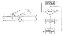
- FIG. 6is a flow diagram showing the process flow for acquiring a frame of touch data from the circuit of FIG. 5 .
- the frameis collected conventionally by driving each of the X lines in turn.
- chargeis accumulated for each Y line on the respective measurement capacitor 112 . n .
- the capacitance accumulatedis then determined by the controller 118 to obtain Y values for the sensing nodes on that X line. This process is then repeated until all X lines have been driven, at which point a full touch data set or frame has been collected comprising one signal value for each of the m ⁇ n sensing nodes on the touch panel.
- Step S 2the controller 118 determines whether a touch has taken place by analyzing the touch data set to establish whether there has been an above-threshold signal on any of the sensing nodes.
- Reference to touchshould not be interpreted literally and should include non-touching proximity of a body. Any sensing node having an above-threshold signal value is said to be “in detect”. If no touch is detected then the process flow returns to Step S 1 to collect another frame of touch data. If a touch is detected then the process flow proceeds to the next step.
- Step S 3the location of the touch is determined, i.e. the sensing node at which the touch has occurred.
- Step S 4another frame of touch data is collected, but this time not all the X lines are driven, but only those at and adjacent the touch location X detected in the preceding frame.
- the controllermay only drive the X 2 line and the immediately adjacent X lines, namely X 1 and X 3 , thereby to collect a subset of the conventional touch data set.
- Step S 4the process flow returns to Step S 2 to determine whether a touch is detected, and the flow proceeds as before. It is noted that if no touch is detected in a reduced touch data set collected in Step S 4 , this may either be because there is no touch on the touch panel, or because a previous touch has moved from one frame to the next sufficiently quickly to be located on one of the X lines that is not being driven. Whatever the reason, the system will recover by reverting to collection of a full frame whenever no touch is detected in a previous frame.
- FIG. 7is a schematic plot of a key pad array overlaid on the sensor grid of FIG. 5 .
- the touch panelcan be considered to be subdivided into an array of m ⁇ n square keys each centered on one of the sensing nodes 205 .
- the keysmay be real, for example if the touch panel is operating as a keypad, or notional, for example if the touch panel is operating as a surface to sense gestures or drawing activity by a user.
- FIGS. 8A to 8Heach show the key array. In FIGS. 8A to 8H eight successive frames are shown. The location of a detected touch is indicated by shading the touched key.
- FIG. 8Eshows the next time interval corresponding to carrying out Step S 1 to drive all X m in view of the failure to detect a key in the previous (sub-)frame, followed by detection of a touch in Step S 2 at location (8,2).
- An alternative to driving all X m in such circumstanceswould be to drive all X m apart from those polled in Step S 4 , i.e. in the present example to drive lines X 1 X 5 X 6 X 7 and X 8 , i.e. all X lines but X 2 X 3 , and X 4 .
- FIG. 8Hshows the next time interval corresponding to carrying out Step S 1 to drive all X m in view of the failure to detect a key in the previous (sub-)frame.
- FIGS. 8A and 8BFor a touch sensor operating to detect user gestures, it might be imagined that the input in FIGS. 8A and 8B is a flick gesture, and the input at FIGS. 8E and 8F is a tap or press.
- the devicereduces the time needed to acquire each frame by tracking touches in one dimension of the sensor grid, and limiting the X drive to those X lines that are close to the sensed touch.
- Step S 4the controller only collects data from the sense lines at the Y location of the previous touch, and adjacent Y lines.
- the touch sensor forming the basis for the above described embodimentis an example of a so-called active or transverse type capacitive sensor.
- further embodimentsmay also be applicable to so-called passive capacitive sensor arrays.
- Passive or single ended capacitive sensing devicesrely on measuring the capacitance of a sensing electrode to a system reference potential (earth). The principles underlying this technique are described in U.S. Pat. No. 5,730,165 and U.S. Pat. No. 6,466,036, for example in the context of discrete (single node) measurements.
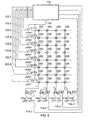
- FIG. 9is a circuit diagram illustrating a touch sensitive matrix providing a two-dimensional capacitive transducing sensor arrangement according to an alternative embodiment.
- a 2D touch-sensitive capacitive position sensor 301is operable to determine the position of objects along a first and a second direction, the orientation of which are shown towards the top left of the drawing.
- the sensor 301comprises a substrate 302 having sensing electrodes 303 arranged thereon.
- the sensing electrodes 303define a sensing area within which the position of an object (e.g. a finger or stylus) to the sensor may be determined.
- the substrate 302is of a transparent plastic material and the electrodes are formed from a transparent film of Indium Tin Oxide (ITO) deposited on the substrate 302 using conventional techniques.
- ITOIndium Tin Oxide
- the sensing area of the sensoris transparent and can be placed over a display screen without obscuring what is displayed behind the sensing area.
- the position sensormay not be intended to be located over a display and may not be transparent; in these instances the ITO layer may be replaced with a more economical material such as a copper laminate Printed Circuit Board (PCB), for example.
- the pattern of the sensing electrodes on the substrate 302is such as to divide the sensing area into an array (grid) of sensing cells 304 arranged into rows and columns.
- arraygrid
- sensing cells 304arranged into rows and columns.
- rows and columnsare used here to conveniently distinguish between two directions and should not be interpreted to imply either a vertical or a horizontal orientation.
- this position sensorthere are three columns of sensing cells aligned with the X-direction and five rows of sensing cells aligned with the Y-direction (fifteen sensing cells in total).
- the top-most row of sensing cellsis referred to as row Y1, the next one down as row Y2, and so on down to row Y 5 .
- the columns of sensing cellsare similarly referred to from left to right as columns X1 to X3.
- Each sensing cellincludes a row sensing electrode 305 and a column sensing electrode 306 .
- the row sensing electrodes 305 and column sensing electrodes 306are arranged within each sensing cell 304 to interleave with one another (in this case by squared spiraling around one another), but are not galvanically connected. Because the row and the column sensing electrodes are interleaved (intertwined), an object adjacent to a given sensing cell can provide a significant capacitive coupling to both sensing electrodes irrespective of where in the sensing cell the object is positioned.
- the characteristic scale of interleavingmay be on the order of, or smaller than, the capacitive footprint of the finger, stylus or other actuating object in order to provide the best results.
- the size and shape of the sensing cell 304can be comparable to that of the object to be detected or larger (within practical limits).
- the row sensing electrodes 305 of all sensing cells in the same roware electrically connected together to form five separate rows of row sensing electrodes.
- the column sensing electrodes 306 of all sensing cells in the same columnare electrically connected together to form three separate columns of column sensing electrodes.
- the position sensor 301further comprises a series of capacitance measurement channels 307 coupled to respective ones of the rows of row sensing electrodes and the columns of column sensing electrodes. Each measurement channel is operable to generate a signal indicative of a value of capacitance between the associated column or row of sensing electrodes and a system ground.
- the capacitance measurement channels 307are shown in FIG. 10 as two separate banks with one bank coupled to the rows of row sensing electrodes (measurement channels labeled Y1 to Y5) and one bank coupled to the columns of column sensing electrodes (measurement channels labeled X1 to X3).
- all of the measurement channel circuitrywill most likely be provided in a single unit such as a programmable or application specific integrated circuit.
- the capacitance measurement channelscould alternatively be provided by a single capacitance measurement channel with appropriate multiplexing.
- circuitry of the kind described in U.S. Pat. No. 5,463,388 or similarcan be used, which drives all the rows and columns with a single oscillator simultaneously in order to propagate a laminar set of sensing fields through the overlying substrate.
- the signals indicative of the capacitance values measured by the measurement channels 307are provided to a controller 308 comprising processing circuitry.
- the position sensorwill be treated as a series of discrete keys or nodes. The position of each discrete key or nodes is the intersection of the x- and y-conducting lines.
- the processing circuitryis configured to determine which of the discrete keys or nodes has a signal indicative of capacitance associated with it.
- the processed datacan then be output by the controller 309 to other systems components on output line 310 .
- the controller 309is operable to output the coordinates on the output connection.
- the host controllermay be a single logic device such as a microcontroller.
- the microcontrollermay have a push-pull type CMOS pin structure, and an input which can be made to act as a voltage comparator. Most common microcontroller I/O ports are capable of this, as they have a relatively fixed input threshold voltage as well as nearly ideal MOSFET switches.
- the necessary functionsmay be provided by a single general purpose programmable microprocessor, microcontroller or other integrated chip, for example a field programmable gate array (FPGA) or application specific integrated chip (ASIC).
- FPGAfield programmable gate array
- ASICapplication specific integrated chip
- FIG. 10is a flow diagram showing the process flow for acquiring a frame of touch data from the circuit of FIG. 9 .
- the process flowis in many respects similar to that shown in FIG. 6 , but reflects the differences between the sensor arrays of FIGS. 5 and 9 .
- the frameis collected conventionally by measuring capacitance on each of the sensing nodes.
- Step S 2the controller 308 determines whether a touch has taken place by analyzing the touch data set to establish whether there has been an above threshold signal on any of the sensing nodes. If no touch is detected then the process flow returns to Step S 1 to collect another frame of touch data. If a touch is detected then the process flow proceeds to the next step.
- Step S 3the location of the touch is determined, i.e. the sensing node at which the touch has occurred.
- Step S 4another frame of touch data is collected, but this time not all the sensing nodes X, Y are sampled, but only those at and adjacent the touch location X, Y detected in the preceding frame. For example, if the touch location detected in the preceding frame is (2,4), then in Step S 4 , the controller may only collect signals from sensing nodes (1,3) (1,4) (1,5) (2,3) (2,4) (2,5) (3,3) (3,4) and (3,5), i.e. the sensing nodes immediately adjacent (2,4), thereby to collect a subset of the conventional touch data set. It will be appreciated that the benefits of the approach in terms of saving acquisition time become relatively greater, the larger the array size, i.e. the greater the product of m and n.
- Step S 4the process flow returns to Step S 2 to determine whether a touch is detected, and the flow proceeds as before. It is noted that if no touch is detected in a reduced touch data set collected in Step S 4 , this may either be because there is no touch on the touch panel, or because a previous touch has moved from one frame to the next sufficiently quickly to be located on one of the sensor nodes or cells that are not being sampled. Whatever the reason, the system will recover, since it reverts to collecting a full frame if no touch is detected in a previous frame.
- Equation 1is the signal value of the discrete keys.
- Midis the signal value of the discrete key with the highest signal value that is adjacent to ‘Max’.
- Minis the ‘zero’ signal value which was defined previously.
- P 0is the offset which corresponds to the nearest x- or y-conducting line.
- P 00 for Y1
- P 01 for Y2
- Qis a number, representing a number of predefined discrete positions within each the discrete keys.
- the above interpolation method, or other method of calculating the touch coordinates at higher resolution than the internode spacing,may be carried out on the full or partial frames of touch data collected according to various embodiments.
Landscapes
- Engineering & Computer Science (AREA)
- Theoretical Computer Science (AREA)
- General Engineering & Computer Science (AREA)
- Human Computer Interaction (AREA)
- Physics & Mathematics (AREA)
- General Physics & Mathematics (AREA)
- Position Input By Displaying (AREA)
- Electronic Switches (AREA)
- Measurement Of Length, Angles, Or The Like Using Electric Or Magnetic Means (AREA)
Abstract
Description
Claims (17)
Priority Applications (4)
| Application Number | Priority Date | Filing Date | Title |
|---|---|---|---|
| US12/501,296US8610009B2 (en) | 2008-10-22 | 2009-07-10 | Capacitive touch sensors |
| TW098135838ATW201023012A (en) | 2008-10-22 | 2009-10-22 | Capacitive touch sensors |
| PCT/GB2009/002521WO2010046650A2 (en) | 2008-10-22 | 2009-10-22 | Capacitive touch sensors |
| US14/094,443US8937611B2 (en) | 2008-10-22 | 2013-12-02 | Capacitive touch sensors |
Applications Claiming Priority (2)
| Application Number | Priority Date | Filing Date | Title |
|---|---|---|---|
| US10738808P | 2008-10-22 | 2008-10-22 | |
| US12/501,296US8610009B2 (en) | 2008-10-22 | 2009-07-10 | Capacitive touch sensors |
Related Child Applications (1)
| Application Number | Title | Priority Date | Filing Date |
|---|---|---|---|
| US14/094,443ContinuationUS8937611B2 (en) | 2008-10-22 | 2013-12-02 | Capacitive touch sensors |
Publications (2)
| Publication Number | Publication Date |
|---|---|
| US20100096193A1 US20100096193A1 (en) | 2010-04-22 |
| US8610009B2true US8610009B2 (en) | 2013-12-17 |
Family
ID=42107742
Family Applications (2)
| Application Number | Title | Priority Date | Filing Date |
|---|---|---|---|
| US12/501,296Active2031-10-08US8610009B2 (en) | 2008-10-22 | 2009-07-10 | Capacitive touch sensors |
| US14/094,443ActiveUS8937611B2 (en) | 2008-10-22 | 2013-12-02 | Capacitive touch sensors |
Family Applications After (1)
| Application Number | Title | Priority Date | Filing Date |
|---|---|---|---|
| US14/094,443ActiveUS8937611B2 (en) | 2008-10-22 | 2013-12-02 | Capacitive touch sensors |
Country Status (3)
| Country | Link |
|---|---|
| US (2) | US8610009B2 (en) |
| TW (1) | TW201023012A (en) |
| WO (1) | WO2010046650A2 (en) |
Cited By (3)
| Publication number | Priority date | Publication date | Assignee | Title |
|---|---|---|---|---|
| US20120247919A1 (en)* | 2009-12-18 | 2012-10-04 | Otis Elevator Company | Detection of people relative to a passenger conveyor with a capacitive sensor |
| US20130181947A1 (en)* | 2011-12-21 | 2013-07-18 | Samsung Electro-Mechanics Co., Ltd. | Touch screen panel |
| US9229597B2 (en) | 2013-02-22 | 2016-01-05 | Nthdegree Technologies Worldwide, Inc. | Integrated capacitive touch screen and LED layer |
Families Citing this family (47)
| Publication number | Priority date | Publication date | Assignee | Title |
|---|---|---|---|---|
| US8352400B2 (en) | 1991-12-23 | 2013-01-08 | Hoffberg Steven M | Adaptive pattern recognition based controller apparatus and method and human-factored interface therefore |
| US7904187B2 (en) | 1999-02-01 | 2011-03-08 | Hoffberg Steven M | Internet appliance system and method |
| US20110096174A1 (en)* | 2006-02-28 | 2011-04-28 | King Martin T | Accessing resources based on capturing information from a rendered document |
| US8941394B2 (en)* | 2008-06-25 | 2015-01-27 | Silicon Laboratories Inc. | Capacitive sensor system with noise reduction |
| US8610009B2 (en) | 2008-10-22 | 2013-12-17 | Atmel Corporation | Capacitive touch sensors |
| US9199608B2 (en)* | 2009-08-21 | 2015-12-01 | Uusi, Llc | Keyless entry assembly having capacitance sensor operative for detecting objects |
| US9845629B2 (en)* | 2009-08-21 | 2017-12-19 | Uusi, Llc | Vehicle keyless entry assembly having capacitance sensor operative for detecting objects |
| US9575481B2 (en) | 2009-08-21 | 2017-02-21 | Uusi, Llc | Fascia panel assembly having capacitance sensor operative for detecting objects |
| US11634937B2 (en) | 2009-08-21 | 2023-04-25 | Uusi, Llc | Vehicle assembly having a capacitive sensor |
| US10017977B2 (en) | 2009-08-21 | 2018-07-10 | Uusi, Llc | Keyless entry assembly having capacitance sensor operative for detecting objects |
| US10954709B2 (en) | 2009-08-21 | 2021-03-23 | Uusi, Llc | Vehicle assembly having a capacitive sensor |
| US9051769B2 (en) | 2009-08-21 | 2015-06-09 | Uusi, Llc | Vehicle assembly having a capacitive sensor |
| US12320180B2 (en) | 2009-08-21 | 2025-06-03 | Uusi, Llc | Vehicle assembly having a capacitive sensor |
| US9705494B2 (en) | 2009-08-21 | 2017-07-11 | Uusi, Llc | Vehicle assemblies having fascia panels with capacitance sensors operative for detecting proximal objects |
| CN101968530B (en)* | 2010-09-30 | 2012-10-17 | 江苏惠通集团有限责任公司 | Key detection method and device |
| DE102011108153A1 (en) | 2011-07-22 | 2013-01-24 | Polyic Gmbh & Co. Kg | Multi-layer body |
| US9612265B1 (en) | 2011-09-23 | 2017-04-04 | Cypress Semiconductor Corporation | Methods and apparatus to detect a conductive object |
| US8903679B2 (en) | 2011-09-23 | 2014-12-02 | Cypress Semiconductor Corporation | Accuracy in a capacitive sense array |
| DE102011122110B4 (en) | 2011-12-22 | 2023-05-25 | Polyic Gmbh & Co. Kg | Operating device with display device and touch panel device, and multi-layer body for providing a touch panel functionality |
| CN103593097B (en)* | 2012-11-29 | 2017-03-01 | 敦泰科技有限公司 | A kind of touch detecting system of terminal unit and terminal unit |
| US20140204046A1 (en)* | 2013-01-22 | 2014-07-24 | Pixart Imaging Inc. | Capacitive touch sensing device and detection method thereof |
| US8717325B1 (en) | 2013-02-18 | 2014-05-06 | Atmel Corporation | Detecting presence of an object in the vicinity of a touch interface of a device |
| US10352976B2 (en)* | 2013-03-15 | 2019-07-16 | Microchip Technology Incorporated | Matrix electrode design for three-dimensional e-filed sensor |
| CN105518599B (en) | 2013-07-08 | 2019-02-19 | 电子触控产品解决方案 | Multi-User Multi-Touch Inductive Capacitive Touch Sensor |
| US9495050B1 (en) | 2013-09-10 | 2016-11-15 | Monterey Research, Llc | Sensor pattern with signal-spreading electrodes |
| US8872526B1 (en)* | 2013-09-10 | 2014-10-28 | Cypress Semiconductor Corporation | Interleaving sense elements of a capacitive-sense array |
| US9367190B2 (en)* | 2013-09-13 | 2016-06-14 | Apex Material Technology Corp. | Touch recognition method and system for a capacitive touch apparatus |
| US9164137B2 (en)* | 2013-12-05 | 2015-10-20 | Parade Technologies, Ltd. | Tunable baseline compensation scheme for touchscreen controllers |
| US9354734B2 (en) | 2014-03-04 | 2016-05-31 | Atmel Corporation | Common-mode hover detection |
| US9256332B2 (en) | 2014-03-19 | 2016-02-09 | Pixart Imaging Inc. | Concurrent driving capacitive touch sensing device capable of resending drive signals |
| US9952732B2 (en) | 2014-12-10 | 2018-04-24 | Pixart Imaging Inc. | Capacitive touch device, capacitive communication device and communication system |
| US9389742B2 (en)* | 2014-12-10 | 2016-07-12 | Pixart Imaging Inc. | Capacitive touch device, capacitive communication device and communication system |
| US9800292B2 (en) | 2014-12-10 | 2017-10-24 | Pixart Imaging Inc | Capacitive communication system and Bluetooth pairing method |
| US11710748B2 (en) | 2015-01-27 | 2023-07-25 | Beijing Boe Optoelectronics Technology Co., Ltd. | Array substrate and touch panel and manufacturing method of array substrate |
| CN104536636B (en) | 2015-01-27 | 2017-12-08 | 京东方科技集团股份有限公司 | A kind of preparation method of array base palte, contact panel and array base palte |
| US10505564B2 (en)* | 2015-02-03 | 2019-12-10 | Texas Instruments Incorporated | Touch keypad with key scanning |
| US9665174B2 (en)* | 2015-02-20 | 2017-05-30 | Sony Interactive Entertainment Inc. | Magnetic tracking of glove fingertips with peripheral devices |
| US9652038B2 (en) | 2015-02-20 | 2017-05-16 | Sony Interactive Entertainment Inc. | Magnetic tracking of glove fingertips |
| CN104883732B (en)* | 2015-04-14 | 2019-05-17 | 哈尔滨工程大学 | A kind of enhanced indoor passive passive human body localization method |
| US9606671B2 (en)* | 2015-04-28 | 2017-03-28 | Pixart Imaging Inc. | Capacitive sensing device capable of eliminating influence from mutual capacitance and operating method thereof |
| TWI669640B (en)* | 2016-11-03 | 2019-08-21 | 禾瑞亞科技股份有限公司 | Touch panel, touch screen and electronic system |
| CN108700973B (en)* | 2016-12-22 | 2021-07-23 | 深圳市汇顶科技股份有限公司 | Capacitance detection circuit and electronic device |
| US10282021B2 (en)* | 2017-06-16 | 2019-05-07 | Synaptics Incorporated | Input object based increase in ground mass state |
| JP6858322B2 (en)* | 2017-12-04 | 2021-04-14 | 株式会社ユピテル | Electronics |
| US10908057B2 (en) | 2018-09-04 | 2021-02-02 | Microchip Technology Incorporated | Activating a submersible sensor based on electrode output, and related systems, methods and devices |
| US11264986B1 (en)* | 2020-11-11 | 2022-03-01 | Nxp Usa, Inc. | Capacitive touch sensing with high safety integrity |
| USD1073985S1 (en) | 2022-10-18 | 2025-05-06 | Uusi, Llc | Sensor weather seal |
Citations (29)
| Publication number | Priority date | Publication date | Assignee | Title |
|---|---|---|---|---|
| US4290052A (en)* | 1979-10-26 | 1981-09-15 | General Electric Company | Capacitive touch entry apparatus having high degree of personal safety |
| US4591833A (en) | 1981-08-13 | 1986-05-27 | Tokyo Shibaura Denki Kabushiki Kaisha | Keyboard unit control system using block scanning techniques |
| US4914624A (en)* | 1988-05-06 | 1990-04-03 | Dunthorn David I | Virtual button for touch screen |
| US5463388A (en) | 1993-01-29 | 1995-10-31 | At&T Ipm Corp. | Computer mouse or keyboard input device utilizing capacitive sensors |
| US5526294A (en)* | 1989-04-28 | 1996-06-11 | Matsushita Electric Industrial Co., Ltd. | Capacitive touch entry apparatus using drive pulse signals of different phases |
| US5730165A (en) | 1995-12-26 | 1998-03-24 | Philipp; Harald | Time domain capacitive field detector |
| US5880411A (en)* | 1992-06-08 | 1999-03-09 | Synaptics, Incorporated | Object position detector with edge motion feature and gesture recognition |
| WO2000044018A1 (en) | 1999-01-26 | 2000-07-27 | Harald Philipp | Capacitive sensor and array |
| US6323846B1 (en)* | 1998-01-26 | 2001-11-27 | University Of Delaware | Method and apparatus for integrating manual input |
| US6466036B1 (en) | 1998-11-25 | 2002-10-15 | Harald Philipp | Charge transfer capacitance measurement circuit |
| US20060007023A1 (en) | 2004-07-08 | 2006-01-12 | Wright David G | Method and apparatus for scanning a key or button matrix |
| US7006078B2 (en)* | 2002-05-07 | 2006-02-28 | Mcquint, Inc. | Apparatus and method for sensing the degree and touch strength of a human body on a sensor |
| US20080158167A1 (en) | 2007-01-03 | 2008-07-03 | Apple Computer, Inc. | Simultaneous sensing arrangement |
| US20090315854A1 (en) | 2008-06-18 | 2009-12-24 | Epson Imaging Devices Corporation | Capacitance type input device and display device with input function |
| US7663607B2 (en) | 2004-05-06 | 2010-02-16 | Apple Inc. | Multipoint touchscreen |
| WO2010046650A2 (en) | 2008-10-22 | 2010-04-29 | Peter Timothy Sleeman | Capacitive touch sensors |
| US7875814B2 (en) | 2005-07-21 | 2011-01-25 | Tpo Displays Corp. | Electromagnetic digitizer sensor array structure |
| US7920129B2 (en) | 2007-01-03 | 2011-04-05 | Apple Inc. | Double-sided touch-sensitive panel with shield and drive combined layer |
| US8031094B2 (en) | 2009-09-11 | 2011-10-04 | Apple Inc. | Touch controller with improved analog front end |
| US8031174B2 (en) | 2007-01-03 | 2011-10-04 | Apple Inc. | Multi-touch surface stackup arrangement |
| US8035622B2 (en)* | 2008-03-27 | 2011-10-11 | Apple Inc. | SAR ADC with dynamic input scaling and offset adjustment |
| US8040326B2 (en)* | 2007-06-13 | 2011-10-18 | Apple Inc. | Integrated in-plane switching display and touch sensor |
| US8049732B2 (en) | 2007-01-03 | 2011-11-01 | Apple Inc. | Front-end signal compensation |
| US8179381B2 (en) | 2008-02-28 | 2012-05-15 | 3M Innovative Properties Company | Touch screen sensor |
| US20120242592A1 (en) | 2011-03-21 | 2012-09-27 | Rothkopf Fletcher R | Electronic devices with flexible displays |
| WO2012129247A2 (en) | 2011-03-21 | 2012-09-27 | Apple Inc. | Electronic devices with flexible displays |
| US20120243719A1 (en) | 2011-03-21 | 2012-09-27 | Franklin Jeremy C | Display-Based Speaker Structures for Electronic Devices |
| US20120243151A1 (en) | 2011-03-21 | 2012-09-27 | Stephen Brian Lynch | Electronic Devices With Convex Displays |
| US20120242588A1 (en) | 2011-03-21 | 2012-09-27 | Myers Scott A | Electronic devices with concave displays |
Family Cites Families (2)
| Publication number | Priority date | Publication date | Assignee | Title |
|---|---|---|---|---|
| EP1678655B1 (en)* | 2003-09-24 | 2008-11-12 | Authentec, Inc. | Finger biometric sensor with sensor electronics distributed over thin film and monocrystalline substrates and related methods |
| US20100097329A1 (en)* | 2008-10-21 | 2010-04-22 | Martin Simmons | Touch Position Finding Method and Apparatus |
- 2009
- 2009-07-10USUS12/501,296patent/US8610009B2/enactiveActive
- 2009-10-22TWTW098135838Apatent/TW201023012A/enunknown
- 2009-10-22WOPCT/GB2009/002521patent/WO2010046650A2/enactiveApplication Filing
- 2013
- 2013-12-02USUS14/094,443patent/US8937611B2/enactiveActive
Patent Citations (30)
| Publication number | Priority date | Publication date | Assignee | Title |
|---|---|---|---|---|
| US4290052A (en)* | 1979-10-26 | 1981-09-15 | General Electric Company | Capacitive touch entry apparatus having high degree of personal safety |
| US4591833A (en) | 1981-08-13 | 1986-05-27 | Tokyo Shibaura Denki Kabushiki Kaisha | Keyboard unit control system using block scanning techniques |
| US4914624A (en)* | 1988-05-06 | 1990-04-03 | Dunthorn David I | Virtual button for touch screen |
| US5526294A (en)* | 1989-04-28 | 1996-06-11 | Matsushita Electric Industrial Co., Ltd. | Capacitive touch entry apparatus using drive pulse signals of different phases |
| US5880411A (en)* | 1992-06-08 | 1999-03-09 | Synaptics, Incorporated | Object position detector with edge motion feature and gesture recognition |
| US5463388A (en) | 1993-01-29 | 1995-10-31 | At&T Ipm Corp. | Computer mouse or keyboard input device utilizing capacitive sensors |
| US5730165A (en) | 1995-12-26 | 1998-03-24 | Philipp; Harald | Time domain capacitive field detector |
| US6323846B1 (en)* | 1998-01-26 | 2001-11-27 | University Of Delaware | Method and apparatus for integrating manual input |
| US6466036B1 (en) | 1998-11-25 | 2002-10-15 | Harald Philipp | Charge transfer capacitance measurement circuit |
| US6452514B1 (en) | 1999-01-26 | 2002-09-17 | Harald Philipp | Capacitive sensor and array |
| WO2000044018A1 (en) | 1999-01-26 | 2000-07-27 | Harald Philipp | Capacitive sensor and array |
| US7006078B2 (en)* | 2002-05-07 | 2006-02-28 | Mcquint, Inc. | Apparatus and method for sensing the degree and touch strength of a human body on a sensor |
| US7663607B2 (en) | 2004-05-06 | 2010-02-16 | Apple Inc. | Multipoint touchscreen |
| US20060007023A1 (en) | 2004-07-08 | 2006-01-12 | Wright David G | Method and apparatus for scanning a key or button matrix |
| US7875814B2 (en) | 2005-07-21 | 2011-01-25 | Tpo Displays Corp. | Electromagnetic digitizer sensor array structure |
| US20080158167A1 (en) | 2007-01-03 | 2008-07-03 | Apple Computer, Inc. | Simultaneous sensing arrangement |
| US8049732B2 (en) | 2007-01-03 | 2011-11-01 | Apple Inc. | Front-end signal compensation |
| US7920129B2 (en) | 2007-01-03 | 2011-04-05 | Apple Inc. | Double-sided touch-sensitive panel with shield and drive combined layer |
| US8031174B2 (en) | 2007-01-03 | 2011-10-04 | Apple Inc. | Multi-touch surface stackup arrangement |
| US8040326B2 (en)* | 2007-06-13 | 2011-10-18 | Apple Inc. | Integrated in-plane switching display and touch sensor |
| US8179381B2 (en) | 2008-02-28 | 2012-05-15 | 3M Innovative Properties Company | Touch screen sensor |
| US8035622B2 (en)* | 2008-03-27 | 2011-10-11 | Apple Inc. | SAR ADC with dynamic input scaling and offset adjustment |
| US20090315854A1 (en) | 2008-06-18 | 2009-12-24 | Epson Imaging Devices Corporation | Capacitance type input device and display device with input function |
| WO2010046650A2 (en) | 2008-10-22 | 2010-04-29 | Peter Timothy Sleeman | Capacitive touch sensors |
| US8031094B2 (en) | 2009-09-11 | 2011-10-04 | Apple Inc. | Touch controller with improved analog front end |
| US20120242592A1 (en) | 2011-03-21 | 2012-09-27 | Rothkopf Fletcher R | Electronic devices with flexible displays |
| WO2012129247A2 (en) | 2011-03-21 | 2012-09-27 | Apple Inc. | Electronic devices with flexible displays |
| US20120243719A1 (en) | 2011-03-21 | 2012-09-27 | Franklin Jeremy C | Display-Based Speaker Structures for Electronic Devices |
| US20120243151A1 (en) | 2011-03-21 | 2012-09-27 | Stephen Brian Lynch | Electronic Devices With Convex Displays |
| US20120242588A1 (en) | 2011-03-21 | 2012-09-27 | Myers Scott A | Electronic devices with concave displays |
Non-Patent Citations (5)
| Title |
|---|
| "International Application Serial No. PCT/GB2009/002521, Search Report mailed Apr. 27, 2010", 4 pgs. |
| "International Application Serial No. PCT/GB2009/002521, Written Opinion mailed Apr. 27, 2010", 4 pgs. |
| U.S. Appl. No. 61/454,894, filed Mar. 21, 2011, Rothkopf. |
| U.S. Appl. No. 61/454,936, filed Mar. 21, 2011, Myers. |
| U.S. Appl. No. 61/454,950, Mar. 21, 2011, Lynch. |
Cited By (5)
| Publication number | Priority date | Publication date | Assignee | Title |
|---|---|---|---|---|
| US20120247919A1 (en)* | 2009-12-18 | 2012-10-04 | Otis Elevator Company | Detection of people relative to a passenger conveyor with a capacitive sensor |
| JP2013514244A (en)* | 2009-12-18 | 2013-04-25 | オーチス エレベータ カンパニー | Detection of people associated with passenger conveyors with capacitive sensors |
| US9272882B2 (en)* | 2009-12-18 | 2016-03-01 | Otis Elevator Company | Detection of people relative to a passenger conveyor with a capacitive sensor |
| US20130181947A1 (en)* | 2011-12-21 | 2013-07-18 | Samsung Electro-Mechanics Co., Ltd. | Touch screen panel |
| US9229597B2 (en) | 2013-02-22 | 2016-01-05 | Nthdegree Technologies Worldwide, Inc. | Integrated capacitive touch screen and LED layer |
Also Published As
| Publication number | Publication date |
|---|---|
| WO2010046650A2 (en) | 2010-04-29 |
| US20100096193A1 (en) | 2010-04-22 |
| US20140085263A1 (en) | 2014-03-27 |
| TW201023012A (en) | 2010-06-16 |
| WO2010046650A3 (en) | 2010-06-24 |
| US8937611B2 (en) | 2015-01-20 |
Similar Documents
| Publication | Publication Date | Title |
|---|---|---|
| US8610009B2 (en) | Capacitive touch sensors | |
| US9495042B2 (en) | Two-dimensional position sensor | |
| TWI444876B (en) | Two-dimensional position sensor | |
| US8552315B2 (en) | Two-dimensional position sensor | |
| US7986152B2 (en) | Capacitive position sensor | |
| US8860686B2 (en) | Multi-chip touch screens | |
| US10754457B2 (en) | Touch-screen panel with multiple sense units and related methods | |
| US9158407B2 (en) | Capacitive touch panel with a ‘dual layer’ force sensor | |
| US8816986B1 (en) | Multiple touch detection | |
| US20110048813A1 (en) | Two-dimensional position sensor | |
| US20100097329A1 (en) | Touch Position Finding Method and Apparatus | |
| US20100097328A1 (en) | Touch Finding Method and Apparatus | |
| US9170681B2 (en) | Noise reduction method and system of capacitive multi-touch panel | |
| KR20130035885A (en) | Predictive touch surface scanning | |
| TW201841100A (en) | Discriminative controller and driving method for touch panel with array electrodes | |
| US10613695B2 (en) | Integrated touch sensing and force sensing in a touch detection device | |
| CN109669585B (en) | Capacitive touch sensing with conductivity type determination |
Legal Events
| Date | Code | Title | Description |
|---|---|---|---|
| AS | Assignment | Owner name:ATMEL CORPORATION,CALIFORNIA Free format text:ASSIGNMENT OF ASSIGNORS INTEREST;ASSIGNORS:YILMAZ, ESAT;SLEEMAN, PETER;REEL/FRAME:023048/0385 Effective date:20090622 Owner name:ATMEL CORPORATION, CALIFORNIA Free format text:ASSIGNMENT OF ASSIGNORS INTEREST;ASSIGNORS:YILMAZ, ESAT;SLEEMAN, PETER;REEL/FRAME:023048/0385 Effective date:20090622 | |
| STCF | Information on status: patent grant | Free format text:PATENTED CASE | |
| AS | Assignment | Owner name:MORGAN STANLEY SENIOR FUNDING, INC. AS ADMINISTRATIVE AGENT, NEW YORK Free format text:PATENT SECURITY AGREEMENT;ASSIGNOR:ATMEL CORPORATION;REEL/FRAME:031912/0173 Effective date:20131206 Owner name:MORGAN STANLEY SENIOR FUNDING, INC. AS ADMINISTRAT Free format text:PATENT SECURITY AGREEMENT;ASSIGNOR:ATMEL CORPORATION;REEL/FRAME:031912/0173 Effective date:20131206 | |
| CC | Certificate of correction | ||
| AS | Assignment | Owner name:ATMEL CORPORATION, CALIFORNIA Free format text:TERMINATION AND RELEASE OF SECURITY INTEREST IN PATENT COLLATERAL;ASSIGNOR:MORGAN STANLEY SENIOR FUNDING, INC.;REEL/FRAME:038376/0001 Effective date:20160404 | |
| AS | Assignment | Owner name:JPMORGAN CHASE BANK, N.A., AS ADMINISTRATIVE AGENT, ILLINOIS Free format text:SECURITY INTEREST;ASSIGNOR:ATMEL CORPORATION;REEL/FRAME:041715/0747 Effective date:20170208 Owner name:JPMORGAN CHASE BANK, N.A., AS ADMINISTRATIVE AGENT Free format text:SECURITY INTEREST;ASSIGNOR:ATMEL CORPORATION;REEL/FRAME:041715/0747 Effective date:20170208 | |
| FPAY | Fee payment | Year of fee payment:4 | |
| AS | Assignment | Owner name:JPMORGAN CHASE BANK, N.A., AS ADMINISTRATIVE AGENT, ILLINOIS Free format text:SECURITY INTEREST;ASSIGNORS:MICROCHIP TECHNOLOGY INCORPORATED;SILICON STORAGE TECHNOLOGY, INC.;ATMEL CORPORATION;AND OTHERS;REEL/FRAME:046426/0001 Effective date:20180529 Owner name:JPMORGAN CHASE BANK, N.A., AS ADMINISTRATIVE AGENT Free format text:SECURITY INTEREST;ASSIGNORS:MICROCHIP TECHNOLOGY INCORPORATED;SILICON STORAGE TECHNOLOGY, INC.;ATMEL CORPORATION;AND OTHERS;REEL/FRAME:046426/0001 Effective date:20180529 | |
| AS | Assignment | Owner name:WELLS FARGO BANK, NATIONAL ASSOCIATION, AS NOTES COLLATERAL AGENT, CALIFORNIA Free format text:SECURITY INTEREST;ASSIGNORS:MICROCHIP TECHNOLOGY INCORPORATED;SILICON STORAGE TECHNOLOGY, INC.;ATMEL CORPORATION;AND OTHERS;REEL/FRAME:047103/0206 Effective date:20180914 Owner name:WELLS FARGO BANK, NATIONAL ASSOCIATION, AS NOTES C Free format text:SECURITY INTEREST;ASSIGNORS:MICROCHIP TECHNOLOGY INCORPORATED;SILICON STORAGE TECHNOLOGY, INC.;ATMEL CORPORATION;AND OTHERS;REEL/FRAME:047103/0206 Effective date:20180914 | |
| AS | Assignment | Owner name:ATMEL CORPORATION, ARIZONA Free format text:RELEASE OF SECURITY INTEREST IN CERTAIN PATENT RIGHTS;ASSIGNOR:WELLS FARGO BANK, NATIONAL ASSOCIATION, AS NOTES COLLATERAL AGENT;REEL/FRAME:047976/0937 Effective date:20181221 Owner name:ATMEL CORPORATION, ARIZONA Free format text:RELEASE OF SECURITY INTEREST IN CERTAIN PATENT RIGHTS;ASSIGNOR:JPMORGAN CHASE BANK, N.A., AS ADMINISTRATIVE AGENT;REEL/FRAME:047976/0884 Effective date:20181221 Owner name:MICROCHIP TECHNOLOGY INCORPORATED, ARIZONA Free format text:RELEASE OF SECURITY INTEREST IN CERTAIN PATENT RIGHTS;ASSIGNOR:WELLS FARGO BANK, NATIONAL ASSOCIATION, AS NOTES COLLATERAL AGENT;REEL/FRAME:047976/0937 Effective date:20181221 Owner name:MICROCHIP TECHNOLOGY INCORPORATED, ARIZONA Free format text:RELEASE OF SECURITY INTEREST IN CERTAIN PATENT RIGHTS;ASSIGNOR:JPMORGAN CHASE BANK, N.A., AS ADMINISTRATIVE AGENT;REEL/FRAME:047976/0884 Effective date:20181221 | |
| AS | Assignment | Owner name:NEODRON LIMITED, IRELAND Free format text:ASSIGNMENT OF ASSIGNORS INTEREST;ASSIGNORS:MICROCHIP TECHNOLOGY INC.;ATMEL CORPORATION;MICROCHIP TECHNOLOGY GERMANY GMBH;REEL/FRAME:048259/0840 Effective date:20181221 | |
| IPR | Aia trial proceeding filed before the patent and appeal board: inter partes review | Free format text:TRIAL NO: IPR2020-00225 Opponent name:SAMSUNG ELECTRONICS CO., LTD. AND SAMSUNG ELECTRON Effective date:20191205 | |
| MAFP | Maintenance fee payment | Free format text:PAYMENT OF MAINTENANCE FEE, 8TH YEAR, LARGE ENTITY (ORIGINAL EVENT CODE: M1552); ENTITY STATUS OF PATENT OWNER: LARGE ENTITY Year of fee payment:8 | |
| AS | Assignment | Owner name:MICROSEMI STORAGE SOLUTIONS, INC., ARIZONA Free format text:RELEASE BY SECURED PARTY;ASSIGNOR:JPMORGAN CHASE BANK, N.A., AS ADMINISTRATIVE AGENT;REEL/FRAME:059333/0222 Effective date:20220218 Owner name:MICROSEMI CORPORATION, ARIZONA Free format text:RELEASE BY SECURED PARTY;ASSIGNOR:JPMORGAN CHASE BANK, N.A., AS ADMINISTRATIVE AGENT;REEL/FRAME:059333/0222 Effective date:20220218 Owner name:ATMEL CORPORATION, ARIZONA Free format text:RELEASE BY SECURED PARTY;ASSIGNOR:JPMORGAN CHASE BANK, N.A., AS ADMINISTRATIVE AGENT;REEL/FRAME:059333/0222 Effective date:20220218 Owner name:SILICON STORAGE TECHNOLOGY, INC., ARIZONA Free format text:RELEASE BY SECURED PARTY;ASSIGNOR:JPMORGAN CHASE BANK, N.A., AS ADMINISTRATIVE AGENT;REEL/FRAME:059333/0222 Effective date:20220218 Owner name:MICROCHIP TECHNOLOGY INCORPORATED, ARIZONA Free format text:RELEASE BY SECURED PARTY;ASSIGNOR:JPMORGAN CHASE BANK, N.A., AS ADMINISTRATIVE AGENT;REEL/FRAME:059333/0222 Effective date:20220218 | |
| AS | Assignment | Owner name:ATMEL CORPORATION, ARIZONA Free format text:RELEASE BY SECURED PARTY;ASSIGNOR:JPMORGAN CHASE BANK, N.A., AS ADMINISTRATIVE AGENT;REEL/FRAME:059262/0105 Effective date:20220218 | |
| AS | Assignment | Owner name:MICROSEMI STORAGE SOLUTIONS, INC., ARIZONA Free format text:RELEASE BY SECURED PARTY;ASSIGNOR:WELLS FARGO BANK, NATIONAL ASSOCIATION, AS NOTES COLLATERAL AGENT;REEL/FRAME:059358/0001 Effective date:20220228 Owner name:MICROSEMI CORPORATION, ARIZONA Free format text:RELEASE BY SECURED PARTY;ASSIGNOR:WELLS FARGO BANK, NATIONAL ASSOCIATION, AS NOTES COLLATERAL AGENT;REEL/FRAME:059358/0001 Effective date:20220228 Owner name:ATMEL CORPORATION, ARIZONA Free format text:RELEASE BY SECURED PARTY;ASSIGNOR:WELLS FARGO BANK, NATIONAL ASSOCIATION, AS NOTES COLLATERAL AGENT;REEL/FRAME:059358/0001 Effective date:20220228 Owner name:SILICON STORAGE TECHNOLOGY, INC., ARIZONA Free format text:RELEASE BY SECURED PARTY;ASSIGNOR:WELLS FARGO BANK, NATIONAL ASSOCIATION, AS NOTES COLLATERAL AGENT;REEL/FRAME:059358/0001 Effective date:20220228 Owner name:MICROCHIP TECHNOLOGY INCORPORATED, ARIZONA Free format text:RELEASE BY SECURED PARTY;ASSIGNOR:WELLS FARGO BANK, NATIONAL ASSOCIATION, AS NOTES COLLATERAL AGENT;REEL/FRAME:059358/0001 Effective date:20220228 | |
| MAFP | Maintenance fee payment | Free format text:PAYMENT OF MAINTENANCE FEE, 12TH YEAR, LARGE ENTITY (ORIGINAL EVENT CODE: M1553); ENTITY STATUS OF PATENT OWNER: LARGE ENTITY Year of fee payment:12 |